WO2014080478A1 - 発光装置及び発光装置の製造方法 - Google Patents
発光装置及び発光装置の製造方法 Download PDFInfo
- Publication number
- WO2014080478A1 WO2014080478A1 PCT/JP2012/080197 JP2012080197W WO2014080478A1 WO 2014080478 A1 WO2014080478 A1 WO 2014080478A1 JP 2012080197 W JP2012080197 W JP 2012080197W WO 2014080478 A1 WO2014080478 A1 WO 2014080478A1
- Authority
- WO
- WIPO (PCT)
- Prior art keywords
- light
- light emitting
- emitting device
- electrode
- layer
- Prior art date
- Legal status (The legal status is an assumption and is not a legal conclusion. Google has not performed a legal analysis and makes no representation as to the accuracy of the status listed.)
- Ceased
Links
Images



Classifications
-
- H—ELECTRICITY
- H10—SEMICONDUCTOR DEVICES; ELECTRIC SOLID-STATE DEVICES NOT OTHERWISE PROVIDED FOR
- H10K—ORGANIC ELECTRIC SOLID-STATE DEVICES
- H10K59/00—Integrated devices, or assemblies of multiple devices, comprising at least one organic light-emitting element covered by group H10K50/00
- H10K59/80—Constructional details
- H10K59/875—Arrangements for extracting light from the devices
- H10K59/878—Arrangements for extracting light from the devices comprising reflective means
-
- H—ELECTRICITY
- H10—SEMICONDUCTOR DEVICES; ELECTRIC SOLID-STATE DEVICES NOT OTHERWISE PROVIDED FOR
- H10K—ORGANIC ELECTRIC SOLID-STATE DEVICES
- H10K50/00—Organic light-emitting devices
- H10K50/10—OLEDs or polymer light-emitting diodes [PLED]
- H10K50/11—OLEDs or polymer light-emitting diodes [PLED] characterised by the electroluminescent [EL] layers
-
- H—ELECTRICITY
- H10—SEMICONDUCTOR DEVICES; ELECTRIC SOLID-STATE DEVICES NOT OTHERWISE PROVIDED FOR
- H10K—ORGANIC ELECTRIC SOLID-STATE DEVICES
- H10K59/00—Integrated devices, or assemblies of multiple devices, comprising at least one organic light-emitting element covered by group H10K50/00
- H10K59/80—Constructional details
- H10K59/875—Arrangements for extracting light from the devices
- H10K59/879—Arrangements for extracting light from the devices comprising refractive means, e.g. lenses
Definitions
- the present invention relates to a light emitting device having an organic light emitting layer and a manufacturing method thereof.
- a light emitting device having an organic light emitting layer as one of the light emitting devices.
- this light emitting device it is desired to improve the ratio of light emitted to the outside (light extraction efficiency) of the light generated in the organic light emitting layer.
- Patent Document 1 As a technique for improving the light extraction efficiency, there is a technique described in Patent Document 1.
- the light emitting device described in Patent Literature 1 includes a substrate, an organic functional layer, a cathode, and an anode.
- An anode or a cathode is disposed between the substrate and the organic functional layer, and a cathode or an anode is disposed on the opposite side of the substrate from the organic functional layer.
- Patent Document 1 describes that light extraction efficiency is improved by forming irregularities between the organic functional layer and the anode or between the organic functional layer and the cathode.
- Patent Document 1 The inventor considered that the technique described in Patent Document 1 has the following problems.
- the anode or the cathode has an uneven shape. For this reason, a leakage current may occur between the anode and the cathode.
- the present inventor can change the refractive index of a part of the light-transmitting layer (refractive index changing portion) by irradiating the light-transmitting layer of the light-emitting device with light. We thought that the extraction efficiency could be improved. And in order to irradiate a light ray to the appropriate position of a translucent layer with high precision, it thought that it was necessary to control the irradiation position of a light ray based on a certain reference position.
- An example of a problem to be solved by the present invention is to provide a light emitting device having a structure capable of irradiating a light beam to the light emitting device by controlling the irradiation position of the light beam with high accuracy.
- a light emitting device A substrate, An organic functional layer including at least a light emitting layer and disposed on one side of the substrate; A first electrode disposed on one side of the organic functional layer; A second electrode disposed on the other surface side of the organic functional layer; A control track serving as a guide for irradiating the light emitting device with light; It is a light-emitting device provided with.
- the invention according to claim 10 is: A substrate, An organic functional layer including at least a light emitting layer and disposed on one side of the substrate; A first electrode disposed on one side of the organic functional layer; A second electrode disposed on the other surface side of the organic functional layer; A bus electrode formed in contact with the first electrode; An optical path changing layer disposed between the substrate and the first electrode or between the substrate and the second electrode and changing an optical path of light from the light emitting layer; With The optical path changing layer is The base region, The base region has a different refractive index, and a plurality of refractive index changing portions arranged in the base region, Including In the light emitting device, the plurality of refractive index changing portions include a plurality of refractive index changing portions arranged in parallel with the bus electrode.
- the invention according to claim 11 Irradiating an intermediate product comprising a substrate, a first electrode disposed on one side of the substrate, and a control track with the control track as a guide, Forming an organic functional layer including at least a light emitting layer on one surface side of the first electrode; Forming a second electrode on the opposite side of the first electrode with respect to the organic functional layer; It is a manufacturing method of the light-emitting device which has.
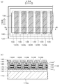
- FIG. 4A is a plan view showing the configuration of the light emitting device according to Example 1
- FIG. 4B is a cross-sectional view taken along the line BB in FIG. 4A
- FIG. 5A is a plan view showing a light emitting layer and a partition wall portion of the light emitting device according to the first embodiment
- FIG. 5B is an example of a process of forming a refractive index changing portion in the A portion of FIG.
- FIG. 6 is a cross-sectional view of a light emitting device according to Example 2.
- FIG. 6 is a cross-sectional view showing a process for manufacturing a light-emitting device according to Example 2.
- FIG. 6 is a cross-sectional view of a light emitting device according to Example 3.
- FIG. 6 is a cross-sectional view showing a process for manufacturing a light emitting device according to Example 3.
- FIG. 6 is a cross-sectional view of a light emitting device according to Example 4.
- FIG. 15A is a cross-sectional view of a light-emitting device according to Example 7
- FIG. 15B is a cross-sectional view of a light-emitting device according to a modification of Example 7.
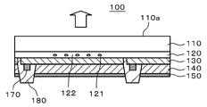
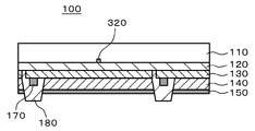
- FIG. 1 is a cross-sectional view of a light emitting device 100 according to an embodiment.
- the light emitting device 100 includes an organic EL (Electro Luminescence) element.
- the light emitting device 100 can be used as a light source of, for example, a display, a lighting device, or an optical communication device.
- the light emitting device 100 is disposed on a substrate (for example, the translucent substrate 110), the organic functional layer 140 disposed on one surface side of the substrate, and the one surface side of the organic functional layer 140.
- the first electrode 130 and the second electrode 150 disposed on the other surface side of the organic functional layer 140 are provided.
- the organic functional layer 140 includes at least a light emitting layer.
- the light emitting device 100 further includes a control track (for example, a bus line (bus electrode) 170) that serves as a guide for irradiating the light emitting device 100 with light.
- a control track for example, a bus line (bus electrode) 170
- the translucent substrate 110 is a plate-like member made of a translucent material such as glass or resin.
- the upper surface of the translucent substrate 110 that is, the surface of the translucent substrate 110 opposite to the organic functional layer 140 is a flat light extraction surface 110a.
- the light extraction surface 110a is in contact with air (refractive index 1) filling the light emission space.
- the light extraction film may be affixed on the upper surface of the translucent board
- the first electrode 130 may be a transparent electrode made of a metal oxide conductor such as ITO (Indium Tin Oxide) or IZO (Indium Zinc Oxide). However, the first electrode 130 may be a metal thin film that is thin enough to transmit light.
- a metal oxide conductor such as ITO (Indium Tin Oxide) or IZO (Indium Zinc Oxide).
- the first electrode 130 may be a metal thin film that is thin enough to transmit light.
- the second electrode 150 is a reflective electrode made of a metal film such as Al.
- the second electrode 150 reflects light traveling from the organic functional layer 140 toward the second electrode 150 toward the translucent substrate 110.
- the light emitting device 100 further includes an optical path changing layer 120 that changes the optical path of light from the light emitting layer.
- the optical path changing layer 120 includes a base region 122 and a refractive index changing portion 121 having a refractive index different from that of the base region 122 when a part of the base region 122 is irradiated with light.
- the optical path changing layer 120 all regions other than the refractive index changing portion 121 are the base region 122.
- the optical path changing layer 120 may include a region other than the refractive index changing portion 121 and the base region 122.
- the optical path changing layer 120 is made of, for example, a dielectric material.
- the optical path changing layer 120 is disposed, for example, between the translucent substrate 110 and the first electrode 130 or between the organic functional layer 140 and the second electrode 150. In the present embodiment, for example, the optical path changing layer 120 is disposed between the translucent substrate 110 and the first electrode 130.
- the light emitting layer of the organic functional layer 140 When a voltage is applied between the first electrode 130 and the second electrode 150, the light emitting layer of the organic functional layer 140 emits light.
- the first electrode 130, the base region 122 of the optical path changing layer 120, the refractive index changing portion 121 of the optical path changing layer 120, the translucent substrate 110, and the organic functional layer 140 are all the light emitting layer of the organic functional layer 140. Transmits at least part of the emitted light. Part of the light emitted from the light emitting layer is emitted (extracted) from the light extraction surface 110a of the translucent substrate 110 to the outside of the light emitting device 100 (that is, the light emission space).
- a plurality of refractive index changing portions 121 are arranged at equal intervals in a plane parallel to the organic functional layer 140.
- the plurality of refractive index changing portions 121 constitute a photonic crystal.
- the plurality of refractive index changing portions 121 constituting the photonic crystal are, for example, distributed in a plane facing the organic functional layer 140.
- the photonic crystal changes the optical path of light in a direction substantially orthogonal to the organic functional layer 140. Therefore, the light extraction efficiency of the light emitting device 100 is improved.
- the size of each refractive index changing portion 121 is ⁇ / 10 or more and smaller than ⁇ / 2.
- the dimension of the refractive index changing portion 121 means the maximum dimension of the outer shape of each refractive index changing portion 121 in plan view.
- the refractive index changing portion 121 may be spherical, and in that case, the dimension is the outer diameter of the refractive index changing portion 121.
- the center-to-center distance between adjacent refractive index changing portions 121 is, for example, ⁇ / 2 or more and ⁇ or less.
- the dimension of the refractive index changing portion 121 may be longer than the emission wavelength from the light emitting layer.
- the optical path of the light is changed in the process of passing through the inside of the refractive index changing unit 121.
- the refractive index changing unit 121 does not exist, the direction of light having an angle that attenuates while repeating the reflection in the light emitting device 100 is changed by the refractive index changing unit 121, so that the light emitting device 100. Can be taken out from. As a result, the light extraction efficiency of the light emitting device 100 is improved.
- the refractive index of the refractive index changing unit 121 is smaller than the refractive index of the base region 122.
- the refractive index difference between the refractive index changing portion 121 and the base region 122 increases as the distance from the boundary between the refractive index changing portion 121 and the base region 122 increases inward. That is, the refractive index of the refractive index changing portion 121 decreases as the distance from the boundary between the refractive index changing portion 121 and the base region 122 increases.
- the refractive index changing portion 121 is formed by irradiating a part of the optical path changing layer 120 (base region 122) with light and heating the part.
- the material of the optical path changing layer 120 for example, a material whose refractive index is lowered by heating can be used.
- the material of the optical path changing layer 120 can be a material having a refractive index equal to or higher than the refractive index of the organic functional layer 140 and having a low refractive index when heated. Examples of such materials include phthalocyanine-based or azo-based organic materials used for DVDs or CDs.
- the optical path changing layer 120 is made of a dielectric, for example. By heating a part of the optical path changing layer 120, the refractive index of the heated part is lowered.
- the refractive index changing portion 121 is a portion where the base region 122 is crystallized, and the refractive index of the refractive index changing portion 121 may be larger than the refractive index of the base region 122.
- the refractive index difference between the refractive index changing portion 121 and the base region 122 increases as the distance from the boundary between the refractive index changing portion 121 and the base region 122 increases inward. . That is, the refractive index of the refractive index changing portion 121 increases as the distance from the boundary between the refractive index changing portion 121 and the base region 122 increases.
- the material of the optical path changing layer 120 (base region 122)
- a material whose refractive index is increased by heating can be used as the material of the optical path changing layer 120 (base region 122).
- the material constituting the optical path changing layer 120 (base region 122) is crystallized.
- the refractive index of the portion becomes higher than the refractive index of the surrounding portion (that is, the base region 122), and gradually increases as the refractive index of the portion moves away from the base region 122, for example.
- NPB N, N-di (naphthalene-1-yl) -N, N-diphenyl-benzidine
- the refractive index changing portion 121 may be a bubble.
- bubbles can be partially formed in the optical path changing layer 120 by heating a part of the optical path changing layer 120 (base region 122) and evaporating the material of the part.
- the bus line 170 is in contact with the surface of the first electrode 130 opposite to the translucent substrate 110.
- a plurality of bus lines 170 extend in parallel to each other.
- the control track is a bus line 170. That is, for example, the first electrode 130 is a transparent electrode, and the control track is a bus electrode formed in contact with the first electrode 130.
- the light emitting device 100 further includes a partition wall 180 that partitions the organic functional layer 140 into a plurality of regions in plan view.
- the partition wall portion 180 is made of an insulating film.
- the partition wall 180 extends along each bus line 170.
- the light emitting device has a plurality of organic functional layers 140.
- these organic functional layers 140 from the organic functional layer 140 disposed on one end side of the light emitting device in a plan view, other light emitting devices.
- a control track (for example, a bus line 170) is arranged in a region up to the organic functional layer 140 arranged on the end side.
- a plurality of organic functional layers 140 in the form of stripes are arranged in parallel with each other, and the control track is arranged in a region between the organic functional layer 140 in the first row and the organic functional layer 140 in the last row, counting from one of them. Is arranged.
- one surface (the lower surface in FIG. 1) of the translucent substrate 110 and one surface (the upper surface in FIG. 1) of the optical path changing layer 120 are in contact with each other.
- the other surface (lower surface in FIG. 1) of the optical path changing layer 120 and one surface (upper surface in FIG. 1) of the first electrode 130 are in contact with each other.
- the other surface (lower surface in FIG. 1) of the first electrode 130 and one surface (upper surface in FIG. 1) of the organic functional layer 140 are in contact with each other.
- the other surface (lower surface in FIG. 1) of the organic functional layer 140 and one surface (upper surface in FIG. 1) of the second electrode 150 are in contact with each other.
- another layer may exist between the translucent substrate 110 and the optical path changing layer 120.
- another layer may exist between the optical path changing layer 120 and the first electrode 130.
- another layer may exist between the first electrode 130 and the organic functional layer 140.
- another layer may exist between the organic functional layer 140 and the second electrode 150.
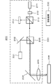
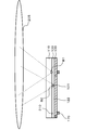
- FIG. 2 is a schematic diagram showing an example of an irradiation device 200 that irradiates a light emitting device with a light beam.
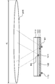
- FIG. 3 is a cross-sectional view showing a process for manufacturing the light emitting device 100 according to the embodiment.
- the irradiation apparatus 200 includes a first laser light source 201, a movable mirror 202, a first beam splitter 203, a mirror 204, a lens 205, a second laser light source 211, a diffraction grating 212, and a second beam splitter 213. And a photodetector 214. Further, the irradiation apparatus 200 includes a first laser light source 201, a movable mirror 202, a first beam splitter 203, a mirror 204, a lens 205, a second laser light source 211, a diffraction grating 212, a second beam splitter 213, and a photodetector 214.
- a moving mechanism 230 that moves the main body 220 relative to the intermediate product 206 in the X direction and the Y direction in the horizontal direction is provided.
- the intermediate product 206 is, for example, the light emitting device 100 after forming the bus line 170 and before forming the organic functional layer 140, the partition wall portion 180, and the second electrode 150, as shown in FIG.
- the diameter dL (FIG. 3) of the lens 205 can be about 8 mm.
- the laser light output from the first laser light source 201 and the laser light output from the second laser light source 211 have different wavelengths.
- the wavelength of the laser light output from the first laser light source 201 is preferably shorter than the wavelength of the laser light output from the second laser light source 211.
- the first laser light source 201 outputs blue laser light
- the second laser light source 211 outputs red laser light.
- the laser light output from the second laser light source 211 is incident on the second beam splitter 213 via the diffraction grating 212, passes through the second beam splitter 213 and the first beam splitter 203 in this order, and is mirrored. The light is reflected at 204, transmitted through the lens 205, and irradiated to the intermediate product 206. Laser light output from the second laser light source 211 is used to control the relative position between the irradiation device 200 and the intermediate product 206. As shown in FIG. 3, the light output from the second laser light source 211 is applied to the bus line 170 as a control track (light beam B1 in FIG. 3).
- This light is reflected by the bus line 170, then passes through the lens 205, is reflected by the mirror 204, passes through the first beam splitter 203, and is reflected by the second beam splitter 213 toward the photodetector 214.
- the photodetector 214 detects the reflected light from the bus line 170 and also detects the irradiation position (beam position) of the reflected light within the detection surface of the photodetector 214.
- the moving mechanism 230 moves the main body 220 along the bus line 170 while correcting the position of the main body 220 so that the beam position in the detection surface of the photodetector 214 is correct by a differential push-pull method or the like.
- the direction of this correction is a direction (X direction in FIG.
- the laser light output from the first laser light source 201 is reflected by the movable mirror 202, reflected by the first beam splitter 203, reflected by the mirror 204, transmitted through the lens 205, and passed through the intermediate product 206. It is irradiated to.
- the laser beam output from the first laser light source 201 is used to form the refractive index changing unit 121. Therefore, this laser light is applied to the base region 122 of the optical path changing layer 120 as shown in FIG.
- the movable mirror 202 may be a type that rotates about an axis, or a type that moves forward and backward.
- the direction in which the irradiation position of the laser beam is changed by the movable mirror 202 is a direction (X direction in FIG. 4A) orthogonal to the extending direction of the control track (the extending direction of the bus line 170). .
- the refractive index changing portion 121 can be formed. That is, as shown in FIG. 3, the refractive index changing portion 121 is formed by irradiating the base region 122 with a light beam B2 such as a laser beam.
- a light beam B2 such as a laser beam.
- the beam diameter of this light is easily reduced. Therefore, the fine refractive index changing portion 121 can be easily formed.
- an organic material such as phthalocyanine-based, azo-based, or NPB is formed on the lower surface of the light-transmitting substrate 110, and a portion that becomes the base region 122 in the optical path changing layer 120 is formed.
- a light-transmitting conductive film made of a metal oxide conductor such as ITO (Indium Tin Oxide) or IZO (Indium Zinc Oxide) is formed on the lower surface of the optical path changing layer 120 (base region 122) by sputtering or the like.
- a first electrode 130 is formed by patterning the film by etching.
- a bus line 170 is formed on the lower surface of the first electrode 130.
- the optical path changing layer 120 is irradiated with light to form the refractive index changing portion 121.
- the position of the bus line 170 is a reference position in a direction (X direction) orthogonal to the extending direction of the bus line 170. Therefore, in this embodiment, the accuracy of the formation position of the refractive index changing portion 121 in the X direction can be improved.
- the molecular structure of the material constituting the optical path changing layer 120 is changed by heating a part of the optical path changing layer 120 (base region 122). Or the density distribution of the material constituting the optical path changing layer 120 changes (the density decreases). That is, the material constituting the optical path changing layer 120 is thermally changed. Thereby, the refractive index of the said part falls.
- the optical path changing layer 120 is configured by heating and cooling a part of the optical path changing layer 120 (base region 122). Crystallization of the material occurs. Thereby, the refractive index of the said part becomes higher than the refractive index of the surrounding part (namely, base region 122).
- the intensity distribution of the irradiated light is a Gaussian distribution, and the intensity at the center of the irradiation spot of the light is increased. For this reason, the closer to the center of the irradiation spot, the greater the influence on the molecular structure, density distribution, etc. of the material constituting the optical path changing layer 120. Therefore, the refractive index of the refractive index changing unit 121 is gradually reduced or increased toward the center of the irradiation spot, for example.
- the organic functional layer 140 is formed by depositing an organic material on the lower surface of the first electrode 130.
- a second electrode 150 is formed by depositing a metal material such as Al in a desired pattern on the lower surface of the organic functional layer 140 by vapor deposition using a mask or the like.
- the partition wall 180 is formed at an appropriate timing. Further, a sealing layer may be formed on the lower surface of the second electrode 150 as necessary.
- the light emitting device manufacturing method includes an intermediate manufacturing method including the substrate (translucent substrate 110), the first electrode 130 disposed on one surface side of the substrate, and the control track (bus line 170).
- the object 206 is irradiated with light using the control track as a guide, the organic functional layer 140 including at least a light emitting layer is formed on one surface side of the first electrode 130, and the organic functional layer 140 as a reference.
- timing which forms the refractive index change part 121 can be made into arbitrary timing after formation of the optical path changing layer 120 (base area
- the refractive index changing portion 121 When the refractive index changing portion 121 is formed after the formation of the optical path changing layer 120 (base region 122) and before the formation of the first electrode 130, light is emitted from any surface side of the optical path changing layer 120 (base region 122). It may be irradiated.
- a translucent substrate is used in order to suppress damage to the first electrode 130 due to light irradiation. Light is irradiated from the 110 side. In any of these cases, the organic functional layer 140 has not yet been formed. For this reason, since it is not necessary to consider the damage to the organic functional layer 140, either a CW laser (continuous wave oscillation operation laser) or a pulse laser may be used.
- the refractive index changing portion 121 may be formed after the sealing is completed and the light emitting device 100 having a panel structure is constructed. In this case, light is irradiated from the translucent substrate 110 side. In this case, in order to use a CW laser or a pulse laser, it is preferable to consider that heat is not applied to the organic functional layer 140 as much as possible. Alternatively, a femtosecond laser or a nanosecond laser may be used.
- the light irradiation for forming the refractive index changing portion 121 is not limited to the laser light irradiation.
- the refractive index changing portion 121 can also be formed by allowing light having a single wavelength other than a laser to pass through a mask and condensing with a lens and forming an image on a part of the optical path changing layer 120. Can do.
- the light emitting device 100 has the bus line 170 as a control track serving as a guide for irradiating the light emitting device 100 with light. Therefore, it is possible to irradiate the light emitting device 100 with light with high accuracy using the bus line 170 as a guide.
- the refractive index changing portion 121 can be formed in the optical path changing layer 120, and the light extraction efficiency of the light emitting device 100 can be improved.
- the manufacturing method of a light-emitting device is an intermediate product 206 including a substrate (translucent substrate 110), a first electrode 130 disposed on one surface side of the substrate, and a control track (bus line 170).
- the step of irradiating light using the control track as a guide the step of forming an organic functional layer 140 including at least a light emitting layer on one surface side of the first electrode 130, and the organic functional layer 140 as a reference.
- the refractive index changing portion 121 can be formed in the optical path changing layer 120, and the light extraction efficiency of the light emitting device 100 can be improved.
- a control track (for example, bus line 170) is arranged.
- the control track is arranged in the effective light emitting area of the light emitting device 100.
- the first electrode 130 is a transparent electrode
- the control track is a bus line (bus electrode) 170 formed so as to be in contact with the first electrode 130. Therefore, the light source 100 can be irradiated with light using the bus line 170 as a guide.
- the light emitting device 100 further includes an optical path changing layer 120 that changes an optical path of light from the light emitting layer.
- the optical path changing layer 120 is irradiated with light rays on the base region 122 and a part of the base region 122.
- a refractive index changing portion 121 having a refractive index different from that of the base region 122. Therefore, the direction of light can be changed by the refractive index changing unit 121, and the light extraction efficiency of the light emitting device 100 can be improved.
- the optical path changing layer 120 is disposed between the substrate (the translucent substrate 110) and the first electrode 130, the direction of light traveling from the light emitting layer toward the substrate is changed by the refractive index changing unit 121.
- the light extraction efficiency of the light emitting device 100 can be improved.
- the optical path changing layer 120 is disposed between the organic functional layer 140 and the second electrode 150, the direction of light traveling from the organic functional layer 140 toward the second electrode 150, or the second electrode 150
- the direction of light reflected and directed toward the organic functional layer 140 can be changed by the refractive index changing unit 121, and the light extraction efficiency of the light emitting device 100 can be improved.
- the light beam forming the refractive index changing portion 121 is a laser beam, the light beam can be collected in an extremely small area, so that the intensity of the light beam can be easily secured and the refractive index changing portion 121 can be easily formed. be able to.
- FIG. 6 is a cross-sectional view showing a first example of the layer structure of the organic functional layer 140.
- the organic functional layer 140 according to this example has a structure in which a hole injection layer 141, a hole transport layer 142, a light emitting layer 143, an electron transport layer 144, and an electron injection layer 145 are stacked in this order. That is, the organic functional layer 140 is an organic electroluminescence light emitting layer. Note that instead of the hole injection layer 141 and the hole transport layer 142, one layer having the functions of these two layers may be provided. Similarly, instead of the electron transport layer 144 and the electron injection layer 145, one layer having the functions of these two layers may be provided (see FIG. 4B).
- the light emitting layer 143 is, for example, a layer that emits red light, a layer that emits blue light, a layer that emits yellow light, or a layer that emits green light.
- a region having a light emitting layer 143 that emits red light, a region having a light emitting layer 143 that emits green light, and a region having a light emitting layer 143 that emits blue light are repeatedly provided. (See FIG. 4B).
- the light emitting device 100 emits light in a single light emission color such as white.
- the light emitting layer 143 may be configured to emit light in a single light emission color such as white by mixing materials for emitting a plurality of colors.
- FIG. 7 is a cross-sectional view showing a second example of the layer structure of the organic functional layer 140.
- the light emitting layer 143 of the organic functional layer 140 in this example has a configuration in which light emitting layers 143a, 143b, and 143c are stacked in this order.
- the light emitting layers 143a, 143b, and 143c emit light of different colors (for example, red, green, and blue).
- the light emitting layers 143a, 143b, and 143c emit light at the same time, so that the light emitting device 100 emits light in a single light emission color such as white.
- the refractive index changing unit 121 corresponds to the peak wavelength of the emission spectrum of the light.
- the area ratio of the region in which the dimension and the center-to-center distance between the adjacent refractive index changing portions 121 are set corresponds to the peak wavelength of another color, and the adjacent refractive index changing portion 121 is adjacent to the size of the refractive index changing portion 121.
- the center-to-center distance is preferably larger than the area ratio of the set region.
- Example 1 In Example 1, an example of a more specific structure of the light emitting device 100 according to the above embodiment will be described.
- FIG. 4A is a plan view showing the light emitting device according to Example 1
- FIG. 4B is a cross-sectional view taken along line BB in FIG. 4A. 4B and 4A are upside down from FIG.
- the light emitting device according to Example 1 is different from the light emitting device 100 according to the embodiment in the points described below, and is otherwise configured in the same manner as the light emitting device 100 according to the embodiment.
- the first electrode 130 constitutes an anode.
- the plurality of first electrodes 130 each extend in the Y direction in a strip shape. Adjacent first electrodes 130 are spaced apart from each other at a constant interval in the X direction orthogonal to the Y direction.
- Each of the first electrodes 130 is made of a metal oxide conductor such as ITO or IZO, for example.
- the refractive index of the first electrode 130 is approximately the same as that of the optical path changing layer 120 (for example, approximately 1.8).
- a bus line 170 for supplying a power supply voltage to the first electrode 130 is formed on each surface of the first electrode 130.
- An insulating film is formed on the optical path changing layer 120 and the first electrode 130.
- a plurality of stripe-shaped openings each extending in the Y direction are formed.
- a plurality of partition walls 180 made of an insulating film are formed.
- Each of the openings formed in the insulating film reaches the first electrode 130, and the surface of each first electrode 130 is exposed at the bottom of the opening.
- An organic functional layer 140 is formed on the first electrode 130 in each opening of the insulating film.
- the organic functional layer 140 is configured by stacking a hole injection layer 141, a hole transport layer 142, a light emitting layer 143 (light emitting layers 143R, 143G, 143B), and an electron transport layer 144 in this order.
- Materials for the hole injection layer 141 and the hole transport layer 142 include aromatic amine derivatives, phthalocyanine derivatives, porphyrin derivatives, oligothiophene derivatives, polythiophene derivatives, benzylphenyl derivatives, compounds in which tertiary amines are linked by fluorene groups, hydrazones. Derivatives, silazane derivatives, silanamine derivatives, phosphamine derivatives, quinacridone derivatives, polyaniline derivatives, polypyrrole derivatives, polyphenylene vinylene derivatives, polythienylene vinylene derivatives, polyquinoline derivatives, polyquinoxaline derivatives, carbon and the like.
- the light emitting layers 143R, 143G, and 143B are made of a fluorescent organometallic compound that emits red light, green light, and blue light, respectively.
- the light emitting layers 143R, 143G, and 143B are arranged side by side in a state of being separated from each other by the partition wall portion 180. That is, the organic functional layer 140 is partitioned into a plurality of regions by the partition wall portion 180.
- An electron transport layer 144 is formed so as to cover the surfaces of the light emitting layers 143R, 143G, and 143B and the partition wall portion 180.
- a second electrode 150 is formed so as to cover the surface of the electron transport layer 144.
- the second electrode 150 constitutes a cathode.
- the second electrode 150 is formed in a band shape.
- the second electrode 150 is made of a metal such as Al or an alloy having a low work function and high reflectivity.
- the refractive index of the organic functional layer 140 is approximately the same as that of the first electrode 130 and the optical path changing layer 120 (for example, a refractive index of approximately 1.8).
- the light emitting layers 143R, 143G, and 143B that emit red, green, and blue light are repeatedly arranged in stripes, and the red, green, and green light is emitted from the surface of the translucent substrate 110 that serves as a light extraction surface.
- Blue light is mixed at an arbitrary ratio to emit light that is recognized as a single emission color (for example, white).
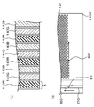
- FIG. 5A is a plan view showing the light-emitting layers 143R, 143G, and 143B and the partition wall portion 180 of the light-emitting device according to Example 1, and FIG. 5B is a refractive index at the portion A in FIG. 5A.
- FIG. 10 is an enlarged plan view showing an example of a process for forming a change part 121.
- a plurality of refractive index changing portions 121 are arranged at equal intervals in a plane parallel to the organic functional layer 140.
- a photonic crystal is formed by the refractive index changing portion 121.
- the refractive index changing portions 121 are formed so that the plurality of refractive index changing portions 121 include a plurality of refractive index changing portions 121 arranged in parallel to the bus line 170. That is, in the light emitting device according to Example 1, the plurality of refractive index changing units 121 include a plurality of refractive index changing units 121 arranged in parallel to the bus electrode.
- the plurality of refractive index changing portions 121 are formed by using the bus line 170 as a guide, it is not necessary to separately form a control track serving as a guide for irradiating light rays.
- the bus line 170 has a high reflectance, reflected light having a good S / N ratio can be obtained, so that the control becomes easy.
- the plurality of refractive index changing portions 121 can be easily formed with high accuracy so as to be arranged in parallel to the bus line 170, and the yield of the light emitting device 100 can be improved.
- FIG. 8 is a cross-sectional view of the light emitting device 100 according to the second embodiment.
- the light-emitting device 100 according to Example 2 is different from the light-emitting device according to the above-described embodiment or Example 1 in the points described below, and is otherwise the same as the light-emitting device according to the embodiment or Example 1. It is configured.
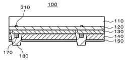
- control track 310 is formed separately from the bus line 170.
- the control track 310 is a layer having a high reflectance such as a metal disposed at a boundary portion between the translucent substrate 110 and the optical path changing layer 120, for example.
- FIG. 9 is a cross-sectional view illustrating a process of manufacturing the light emitting device 100 according to the second embodiment.
- the refractive index changing portion 121 can be formed by the light beam B2 while scanning the control track 310 by the light beam B1.
- control track 310 since the control track 310 is formed separately from the bus line 170, the control track 310 can be formed in an arbitrary arrangement independent of the bus line 170.
- FIG. 10 is a cross-sectional view of the light emitting device 100 according to the third embodiment.
- the light emitting device 100 according to the third embodiment is different from the light emitting device according to the second embodiment in the points described below, and is otherwise configured in the same manner as the light emitting device according to the second embodiment.
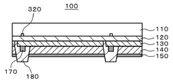
- control track 320 is a groove formed in the light-transmitting substrate 110.
- FIG. 11 is a cross-sectional view illustrating a process of manufacturing the light emitting device 100 according to the third embodiment.
- the refractive index changing portion 121 can be formed by the light beam B2 while detecting the control track 320 using the light beam B1 and moving the main body 220 along the control track 320.
- control track 320 is formed separately from the bus line 170, the control track 310 can be formed in an arbitrary arrangement independent of the bus line 170.
- FIG. 12 is a cross-sectional view of the light emitting device according to the fourth embodiment.
- the control track 320 is arranged at an interval between the bus lines 170 in a plan view, and when the light beam is irradiated to a position far from the bus line 170, the control track 320 is used as a guide.
- the control track 320 is a groove, it does not hinder the emitted light even if it exists at an interval between the bus lines 170.
- FIG. 13 is a plan view illustrating a process of manufacturing the light emitting device according to Example 5, and is an enlarged view of a portion A in FIG.
- the light emitting device 100 according to the fifth embodiment is different from the light emitting device according to the first embodiment in the points described below, and is otherwise configured in the same manner as the light emitting device according to the first embodiment.
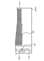
- the bus line (control track) 170 has wobble (position determination information).
- the wobble has a waveform shape that undulates in a direction that intersects the extending direction of the bus line 170.
- the address information can be recognized by detecting the shape of the wobble using the light beam B1.
- address information can be recognized by counting the number of waveforms from the wobble reference point (sync).
- the address in the extending direction of the bus line 170 (the Y direction in FIG. 4A) can be recognized. Therefore, the light beam B2 can be irradiated with high accuracy to the position corresponding to the predetermined address.
- Each waveform of the wobble becomes a reference position in the extending direction of the bus line 170.
- the wobble may be modulated with digital data (address data) (address data) and error correction data may be added.
- the wobble is modulated by Sync, the address data and error correction data converted by the conversion table.
- the address of each block can be specified by a combination of Sync, address data, and error correction data.
- FIG. 14 is a cross-sectional view of the light emitting device 100 according to the sixth embodiment.
- the light emitting device 100 according to Example 6 is different from the light emitting device according to Example 5 (FIG. 13) in the points described below, and is configured in the same manner as the light emitting device according to Example 5 in other points. .
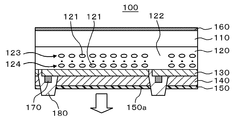
- a light reflecting film 160 is formed on the side of the translucent substrate 110 opposite to the organic functional layer 140 side, that is, on the upper surface side of the translucent substrate 110.
- the light reflecting film 160 is made of a metal film such as Al.
- the second electrode 150 is translucent.
- the second electrode 150 can be, for example, a transparent electrode made of a metal oxide conductor such as ITO or IZO.
- the second electrode 150 may be a metal thin film that is thin enough to transmit light.
- the lower surface of the second electrode 150 is a light extraction surface 150a.
- the optical path changing layer 120 is arranged on the side opposite to the light extraction side (that is, the light extraction surface 150a side) that emits light from the light emitting device 100 to the outside with the organic functional layer 140 as a reference.
- Each of the first surface parallel to the organic functional layer 140 and the second surface parallel to the organic functional layer 140 and spaced from the first surface in the direction perpendicular to the organic functional layer 140 The plurality of refractive index changing portions 121 are arranged at equal intervals.
- the refractive index changing portion 121 can be formed with high accuracy by forming the refractive index changing portion 121 using the address information given to the wobble of the bus line 170.
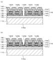
- FIG. 15A is a cross-sectional view of a light-emitting device according to Example 7
- FIG. 15B is a cross-sectional view of a light-emitting device according to a modification of Example 7.
- the light emitting device according to Example 7 is different from the light emitting device according to Example 1 in the points described below, and is configured in the same manner as the light emitting device according to Example 1 in other points.
- the control track can also be used as a guide when repairing the light emitting device. That is, the control track is used to detect the position where repair is to be performed. By using a control track having wobbles, it is possible to detect the position to be repaired with higher accuracy and repair the desired position.
- the control track as a guide, at least a part of at least one of the first electrode 130 and the second electrode 150 is cut by being irradiated with the light beam.
- the second electrode 150 is cut from the first electrode 130.
- only the second electrode 150 of the first electrode 130 and the second electrode 150 is cut. Of the first electrode 130 and the second electrode 150, only the first electrode 130 may be cut.
- the organic EL element is formed very thin, there is a possibility that the first electrode 130 and the second electrode 150 are locally short-circuited. Therefore, when those short-circuited portions are detected, the short-circuit between the first electrode 130 and the second electrode 150 can be eliminated by cutting the short-circuited portion by irradiation of light.
- the physical distance with the wavelength such as ⁇ / 2 as a parameter takes into account the refractive index of each part of the light emitting device. That is, for example, ⁇ / 2 in a material having a refractive index of 1.8 is ⁇ / (2 ⁇ 1.8) as an actual distance.
Landscapes
- Electroluminescent Light Sources (AREA)
Abstract
発光装置(100)は、基板(例えば透光性基板110)と、基板の一方の面側に配置されている有機機能層(140)と、有機機能層(140)の一方の面側に配置された第1電極(130)と、有機機能層(140)の他方の面側に配置された第2電極(150)を備える。有機機能層(140)は、少なくとも発光層を含む。発光装置(100)は、当該発光装置(100)に光線を照射するためのガイドとなる制御トラック(例えばバスライン170)を有する。
Description
本発明は、有機発光層を有する発光装置及びその製造方法に関する。
発光装置の1つに有機発光層を有する発光装置がある。この発光装置においては、有機発光層で発生した光のうち外部に放射される光の割合(光取り出し効率)を向上することが望まれている。
光取り出し効率の向上を目的とした技術としては、特許文献1に記載のものがある。特許文献1に記載された発光装置は、基板と、有機機能層と、陰極及び陽極と、を有している。基板と有機機能層との間には陽極又は陰極が配置され、有機機能層を基準として基板とは反対側には陰極又は陽極が配置されている。特許文献1には、有機機能層と陽極との間、又は、有機機能層と陰極との間に凹凸を形成することにより、光取り出し効率が向上する旨の記載がある。
本発明者は、特許文献1に記載の技術では、以下に説明する問題があると考えた。
特許文献1の技術では、陽極又は陰極が凹凸形状を有する。このため、陽極と陰極との相互間でリーク電流が発生する可能性がある。
特許文献1の技術では、陽極又は陰極が凹凸形状を有する。このため、陽極と陰極との相互間でリーク電流が発生する可能性がある。
また、本発明者は、発光装置が有する透光層に対して光線を照射することによって、その透光層の一部分(屈折率変化部)の屈折率を変化させることができ、これにより、光取り出し効率を向上できると考えた。そして、透光層の適切な位置に光線を高精度に照射するためには、光線の照射位置を、ある基準位置に基づいて制御する必要があると考えた。
本発明が解決しようとする課題としては、光線の照射位置を高精度に制御して発光装置に対して光線を照射することが可能な構造の発光装置を提供することが一例として挙げられる。
請求項1に記載の発明は、
発光装置であって、
基板と、
少なくとも発光層を含み、前記基板の一方の面側に配置されている有機機能層と、
前記有機機能層の一方の面側に配置された第1電極と、
前記有機機能層の他方の面側に配置された第2電極と、
当該発光装置に光線を照射するためのガイドとなる制御トラックと、
を備える発光装置である。
発光装置であって、
基板と、
少なくとも発光層を含み、前記基板の一方の面側に配置されている有機機能層と、
前記有機機能層の一方の面側に配置された第1電極と、
前記有機機能層の他方の面側に配置された第2電極と、
当該発光装置に光線を照射するためのガイドとなる制御トラックと、
を備える発光装置である。
請求項10に記載の発明は、
基板と、
少なくとも発光層を含み、前記基板の一方の面側に配置されている有機機能層と、
前記有機機能層の一方の面側に配置された第1電極と、
前記有機機能層の他方の面側に配置された第2電極と、
前記第1電極に接するように形成されたバス電極と、
前記基板と前記第1電極との間、又は、前記基板と前記第2電極との間に配置され、前記発光層からの光の光路を変更する光路変更層と、
を備え、
前記光路変更層は、
ベース領域と、
前記ベース領域とは屈折率が異なり、前記ベース領域内に配置された複数の屈折率変化部と、
を含み、
前記複数の屈折率変化部には、前記バス電極に対して平行に並ぶ複数の前記屈折率変化部が含まれている発光装置である。
基板と、
少なくとも発光層を含み、前記基板の一方の面側に配置されている有機機能層と、
前記有機機能層の一方の面側に配置された第1電極と、
前記有機機能層の他方の面側に配置された第2電極と、
前記第1電極に接するように形成されたバス電極と、
前記基板と前記第1電極との間、又は、前記基板と前記第2電極との間に配置され、前記発光層からの光の光路を変更する光路変更層と、
を備え、
前記光路変更層は、
ベース領域と、
前記ベース領域とは屈折率が異なり、前記ベース領域内に配置された複数の屈折率変化部と、
を含み、
前記複数の屈折率変化部には、前記バス電極に対して平行に並ぶ複数の前記屈折率変化部が含まれている発光装置である。
請求項11に記載の発明は、
基板と、前記基板の一方の面側に配置された第1電極と、制御トラックと、を備える中間製造物に対して、前記制御トラックをガイドとして光線を照射する工程と、
前記第1電極の一方の面側に、少なくとも発光層を含む有機機能層を形成する工程と、
前記有機機能層を基準として前記第1電極とは反対側に第2電極を形成する工程と、
有する発光装置の製造方法である。
基板と、前記基板の一方の面側に配置された第1電極と、制御トラックと、を備える中間製造物に対して、前記制御トラックをガイドとして光線を照射する工程と、
前記第1電極の一方の面側に、少なくとも発光層を含む有機機能層を形成する工程と、
前記有機機能層を基準として前記第1電極とは反対側に第2電極を形成する工程と、
有する発光装置の製造方法である。
上述した目的、およびその他の目的、特徴および利点は、以下に述べる好適な実施の形態、およびそれに付随する以下の図面によってさらに明らかになる。
以下、実施の形態について、図面を用いて説明する。尚、すべての図面において、同様の構成要素には同一の符号を付し、適宜説明を省略する。
(実施形態)
図1は実施形態に係る発光装置100の断面図である。この発光装置100は、有機EL(Electro Luminescence)素子を含んで構成される。この発光装置100は、例えばディスプレイ、照明装置、又は光通信装置の光源として用いることができる。
図1は実施形態に係る発光装置100の断面図である。この発光装置100は、有機EL(Electro Luminescence)素子を含んで構成される。この発光装置100は、例えばディスプレイ、照明装置、又は光通信装置の光源として用いることができる。
本実施形態に係る発光装置100は、基板(例えば透光性基板110)と、基板の一方の面側に配置されている有機機能層140と、有機機能層140の一方の面側に配置された第1電極130と、有機機能層140の他方の面側に配置された第2電極150と、を備える。有機機能層140は、少なくとも発光層を含む。発光装置100は、更に、当該発光装置100に光線を照射するためのガイドとなる制御トラック(例えばバスライン(バス電極)170)を有する。
以下においては、説明を簡単にするため、発光装置100の各構成要素の位置関係(上下関係等)が各図に示す関係であるものとして説明を行う。ただし、この説明における位置関係は、発光装置100の使用時の位置関係とは無関係である。
透光性基板110は、ガラスや樹脂などの透光性を有する材料からなる板状部材である。本実施形態の場合、透光性基板110の上面、すなわち透光性基板110における有機機能層140とは反対側の面は、平坦な光取り出し面110aとなっている。この光取り出し面110aは、光放出空間を充たす空気(屈折率1)と接している。なお、透光性基板110の上面には、光取り出しフィルムが貼り付けられていて、この光取り出しフィルムの上面が光取り出し面を構成していても良い。
第1電極130は、例えばITO(Indium Tin Oxide)やIZO(Indium Zinc Oxide)などの金属酸化物導電体からなる透明電極とすることができる。ただし、第1電極130は、光が透過する程度に薄い金属薄膜であっても良い。
第2電極150は、例えば、Alなどの金属膜からなる反射電極である。第2電極150は、有機機能層140から第2電極150側に向かう光を、透光性基板110側に向けて反射する。
発光装置100は、更に、発光層からの光の光路を変更する光路変更層120を有している。光路変更層120は、ベース領域122と、ベース領域122の一部分に光線が照射されることによりベース領域122とは異なる屈折率とされた屈折率変化部121と、を含む。
例えば、光路変更層120において、屈折率変化部121以外の領域は、すべてベース領域122となっている。ただし、光路変更層120は、屈折率変化部121及びベース領域122以外の領域を含んで構成されていても良い。光路変更層120は、例えば、誘電体材料により構成されている。
光路変更層120は、例えば、透光性基板110と第1電極130との間、又は、有機機能層140と第2電極150との間に配置されている。本実施形態の場合、例えば、光路変更層120は、透光性基板110と第1電極130との間に配置されている。
第1電極130と第2電極150との間に電圧が印加されることにより、有機機能層140の発光層が発光する。第1電極130、光路変更層120のベース領域122、光路変更層120の屈折率変化部121、透光性基板110、及び、有機機能層140は、いずれも、有機機能層140の発光層が発光した光の少なくとも一部を透過する。発光層が発光した光の一部は、透光性基板110の光取り出し面110aから、発光装置100の外部(つまり上記光放出空間)に放射される(取り出される)。
光路変更層120には、例えば、複数の屈折率変化部121が有機機能層140に対して平行な面内において等間隔に配置されている。これら複数の屈折率変化部121によりフォトニック結晶が構成されている。フォトニック結晶を構成する複数の屈折率変化部121は、例えば、有機機能層140に対して対向する面内において分散して配置されている。この場合、フォトニック結晶は、光の光路を、有機機能層140に対してほぼ直交する方向に変更する。よって、発光装置100の光取り出し効率が向上する。複数の屈折率変化部121がフォトニック結晶を構成する場合、発光層からの光の発光スペクトルのピーク波長(例えば最大ピーク波長)をλとすると、各屈折率変化部121の寸法は、λ/10以上で且つλ/2よりも小さい。ここで、屈折率変化部121の寸法とは、平面視における個々の屈折率変化部121の外形における最大寸法を意味する。一例として、屈折率変化部121は球形であることが挙げられ、その場合、寸法は屈折率変化部121の外径である。また、隣り合う屈折率変化部121どうしの中心間距離は、例えば、λ/2以上λ以下とする。
或いは、屈折率変化部121の寸法は、発光層からの発光波長以上であっても良い。この場合、光の光路は、屈折率変化部121の内部を透過する過程で変更される。この場合、屈折率変化部121が存在しなければ発光装置100内での反射を繰り返すうちに減衰してしまうような角度の光の向きを、屈折率変化部121によって変更して、発光装置100から取り出すことができる。その結果、発光装置100の光取り出し効率が向上する。
例えば、屈折率変化部121の屈折率は、ベース領域122の屈折率よりも小さい。例えば、屈折率変化部121とベース領域122との屈折率差は、屈折率変化部121とベース領域122との境界から屈折率変化部121の内向きに遠ざかるにつれて大きくなっている。すなわち、屈折率変化部121の屈折率は、屈折率変化部121とベース領域122との境界から遠ざかるにつれて低減している。
屈折率変化部121は、光路変更層120(ベース領域122)の一部分に光線を照射して当該一部分を加熱することにより形成されている。したがって、光路変更層120の材料としては、例えば、加熱により屈折率が低下するものを用いることができる。光路変更層120の材料は、有機機能層140の屈折率以上の屈折率を有し、加熱により低屈折率となる材料とすることができる。このような材料の例としては、DVD又はCDなどに用いられるフタロシアニン系又はアゾ系などの有機材料が挙げられる。光路変更層120は、例えば、誘電体からなる。光路変更層120の一部分を加熱することにより、加熱された部分の屈折率が低下する。
屈折率変化部121は、光路変更層120(ベース領域122)の一部分に光線を照射して当該一部分を加熱することにより形成されている。したがって、光路変更層120の材料としては、例えば、加熱により屈折率が低下するものを用いることができる。光路変更層120の材料は、有機機能層140の屈折率以上の屈折率を有し、加熱により低屈折率となる材料とすることができる。このような材料の例としては、DVD又はCDなどに用いられるフタロシアニン系又はアゾ系などの有機材料が挙げられる。光路変更層120は、例えば、誘電体からなる。光路変更層120の一部分を加熱することにより、加熱された部分の屈折率が低下する。
また、屈折率変化部121は、ベース領域122が結晶化した部分であるとともに、屈折率変化部121の屈折率は、ベース領域122の屈折率よりも大きくても良い。例えば、この場合も、屈折率変化部121とベース領域122との屈折率差は、屈折率変化部121とベース領域122との境界から屈折率変化部121の内向きに遠ざかるにつれて大きくなっている。すなわち、屈折率変化部121の屈折率は、屈折率変化部121とベース領域122との境界から遠ざかるにつれて増大している。
この場合、光路変更層120(ベース領域122)の材料としては、加熱により屈折率が高くなるものを用いることができる。このような材料の光路変更層120(ベース領域122)の一部分を、加熱した後で冷却することにより、光路変更層120(ベース領域122)を構成する材料の結晶化が生じる。これにより、当該一部分の屈折率が、その周囲の部分(つまりベース領域122)の屈折率よりも高くなるとともに、例えば、当該一部分の屈折率がベース領域122から遠ざかるにつれて徐々に増大する。光路変更層120の材質としては、例えば、有機機能層140の材料として用いられるNPB(N,N-di(naphthalene-1-yl)-N,N-diphenyl-benzidene)を用いることができる。
この場合、光路変更層120(ベース領域122)の材料としては、加熱により屈折率が高くなるものを用いることができる。このような材料の光路変更層120(ベース領域122)の一部分を、加熱した後で冷却することにより、光路変更層120(ベース領域122)を構成する材料の結晶化が生じる。これにより、当該一部分の屈折率が、その周囲の部分(つまりベース領域122)の屈折率よりも高くなるとともに、例えば、当該一部分の屈折率がベース領域122から遠ざかるにつれて徐々に増大する。光路変更層120の材質としては、例えば、有機機能層140の材料として用いられるNPB(N,N-di(naphthalene-1-yl)-N,N-diphenyl-benzidene)を用いることができる。
また、屈折率変化部121は気泡であっても良い。例えば、光路変更層120(ベース領域122)の一部分を加熱して、当該一部分の材料を蒸発させることによって、光路変更層120に部分的に気泡を形成することができる。
バスライン170は、第1電極130において透光性基板110とは反対側の面に接している。複数のバスライン170が互いに平行に延在している。例えば、制御トラックは、バスライン170である。すなわち、例えば、第1電極130は透明電極であり、制御トラックは、第1電極130に接するように形成されたバス電極である。
発光装置100は、更に、有機機能層140を平面視において複数の領域に仕切る隔壁部180を有している。隔壁部180は、絶縁膜からなる。隔壁部180は、各バスライン170に沿って延在している。
ここで、発光装置は、複数の有機機能層140を有しており、これら有機機能層140のうち、平面視において発光装置の一端側に配置されている有機機能層140から、発光装置の他端側に配置されている有機機能層140までの領域に、制御トラック(例えばバスライン170)が配置されている。例えば、ストライプ状の複数の有機機能層140が互いに並列に配置されており、このうち一方から数えて先頭列の有機機能層140から最後列の有機機能層140までの間の領域に、制御トラックが配置されている。
例えば、透光性基板110の一方の面(図1における下面)と光路変更層120の一方の面(図1における上面)とが相互に接している。また、光路変更層120の他方の面(図1における下面)と第1電極130の一方の面(図1における上面)とが相互に接している。また、第1電極130の他方の面(図1における下面)と有機機能層140の一方の面(図1における上面)とが相互に接している。また、有機機能層140の他方の面(図1における下面)と第2電極150の一方の面(図1における上面)とが相互に接している。ただし、透光性基板110と光路変更層120との間には他の層が存在していても良い。同様に、光路変更層120と第1電極130との間には他の層が存在していても良い。同様に、第1電極130と有機機能層140との間には他の層が存在していても良い。同様に、有機機能層140と第2電極150との間には他の層が存在していても良い。
図2は発光装置に光線を照射する照射装置200の一例を示す模式図である。また、図3は実施形態に係る発光装置100を製造する工程を示す断面図である。
照射装置200は、第1レーザ光源201と、可動ミラー202と、第1ビームスプリッター203と、ミラー204と、レンズ205と、第2レーザ光源211と、回折格子212と、第2ビームスプリッター213と、フォトディテクター214と、を有している。更に、照射装置200は、第1レーザ光源201、可動ミラー202、第1ビームスプリッター203、ミラー204、レンズ205、第2レーザ光源211、回折格子212、第2ビームスプリッター213及びフォトディテクター214からなる本体部220を中間製造物206に対して水平方向におけるX方向及びY方向に相対的に移動させる移動機構230を有している。なお、中間製造物206は、例えば、図3に示すように、バスライン170の形成後、有機機能層140、隔壁部180及び第2電極150を形成する前の発光装置100である。レンズ205の径dL(図3)は、一例として、8mm程度とすることができる。第1レーザ光源201から出力されるレーザ光と、第2レーザ光源211から出力されるレーザ光とは、互いに波長が異なる。第1レーザ光源201から出力されるレーザ光の波長は、第2レーザ光源211から出力されるレーザ光の波長よりも短いことが好ましい。具体的には、例えば、第1レーザ光源201は青色のレーザ光を出力し、第2レーザ光源211は赤色のレーザ光を出力する。
第2レーザ光源211から出力されるレーザ光は、回折格子212を介して第2ビームスプリッター213に入射し、該第2ビームスプリッター213と、第1ビームスプリッター203と、をこの順に透過し、ミラー204にて反射し、レンズ205を透過して、中間製造物206に対して照射される。第2レーザ光源211から出力されるレーザ光は、照射装置200と中間製造物206との相対位置を制御するために用いられる。第2レーザ光源211から出力される光は、図3に示すように、制御トラックとしてのバスライン170に対して照射される(図3の光線B1)。この光は、バスライン170にて反射した後、レンズ205を透過し、ミラー204にて反射し、第1ビームスプリッター203を透過し、第2ビームスプリッター213にてフォトディテクター214側に反射する。フォトディテクター214はバスライン170からの反射光を検出するとともに、当該フォトディテクター214の検出面内における反射光の照射位置(ビーム位置)についても検出する。移動機構230は、ディファレンシャルプッシュプル法などにより、フォトディテクター214の検出面内におけるビーム位置が正しくなるように本体部220の位置を補正しながら、本体部220をバスライン170に沿って移動させる。この補正の方向は、制御トラックの延在方向(バスライン170の延在方向)に対して直交する方向(図4(a)のX方向)である。なお、バスライン170に照射する光として、第1レーザ光源201からのレーザ光とは異なる波長が長い赤色や赤外の光を使用することにより、バスライン170を検出しやすくなる。
第1レーザ光源201から出力されるレーザ光は、可動ミラー202にて反射し、第1ビームスプリッター203にて反射し、ミラー204にて反射し、レンズ205を透過して、中間製造物206に対して照射される。第1レーザ光源201から出力されるレーザ光は、屈折率変化部121を形成するために用いられる。従って、このレーザ光は、図3に示すように、光路変更層120のベース領域122に照射される。可動ミラー202は、軸を中心として回転するタイプであっても良いし、進退移動するタイプであっても良い。なお、可動ミラー202によりレーザ光の照射位置を変更する方向は、制御トラックの延在方向(バスライン170の延在方向)に対して直交する方向(図4(a)のX方向)である。
可動ミラー202によりベース領域122に対するレーザ光の照射位置を変更しながら(レーザ光を走査しながら)、所定の間隔でレーザ光の照射強度を増大することにより、所定の間隔でベース領域122を熱的に変化させて屈折率変化部121を形成することができる。すなわち、図3に示すように、レーザ光などの光線B2をベース領域122に照射することにより、屈折率変化部121が形成されている。なお、屈折率変化部121を形成するための光として、第2レーザ光源211から出力されるレーザ光よりも波長が短い青色の光を使用することにより、この光のビーム径を容易に細くすることができ、容易に微細な屈折率変化部121を形成することができる。
次に、実施形態に係る発光装置100を製造する工程の全体の流れの一例を説明する。
先ず、透光性基板110の下面に、フタロシアニン系、アゾ系又はNPBなどの有機材料を成膜し、光路変更層120におけるベース領域122となる部分を形成する。
次に、光路変更層120(ベース領域122)の下面に、スパッタ法などによりITO(Indium Tin Oxide)やIZO(Indium Zinc Oxide)などの金属酸化物導電体からなる透光性の導電膜を成膜し、エッチングによりこれをパターニングして第1電極130を形成する。
次に、第1電極130の下面にバスライン170を形成する。
次に、バスライン170を、光路変更層120に光線を照射するためのガイドとして用いながら、光路変更層120に光線を照射し、屈折率変化部121を形成する。ここで、バスライン170の位置は、バスライン170の延在方向に対して直交する方向(X方向)における基準位置となる。よって、本実施形態では、X方向における屈折率変化部121の形成位置の精度を向上することができる。
光路変更層120の材料として、加熱により屈折率が低下するものを用いた場合、光路変更層120(ベース領域122)の一部分を加熱することにより、光路変更層120を構成する材料の分子構造が変化したり、或いは、光路変更層120を構成する材料の粗密分布が変化(密度が低下)したりする。すなわち、光路変更層120を構成する材料が熱的に変化する。これにより、当該一部分の屈折率が低下する。
また、光路変更層120の材料として、加熱により屈折率が高くなるものを用いた場合、光路変更層120(ベース領域122)の一部分を加熱した後で冷却することにより、光路変更層120を構成する材料の結晶化が生じる。これにより、当該一部分の屈折率が、その周囲の部分(つまりベース領域122)の屈折率よりも高くなる。
ここで、照射される光(レーザ光等)の強度分布はガウシアン分布であり、当該光の照射スポットの中心部の強度が高くなる。このため、照射スポットの中央に近いほど、光路変更層120を構成する材料の分子構造や粗密分布等に与える影響が大きい。よって、屈折率変化部121の屈折率は、例えば、照射スポットの中心に向けて徐々に低減又は増大する。
また、光路変更層120(ベース領域122)の一部分を加熱して、当該一部分の材料を蒸発させることによって、光路変更層120に部分的に気泡を形成し、この気泡を屈折率変化部121としても良い。
次に、第1電極130の下面に有機材料を成膜することにより有機機能層140を形成する。
次に、有機機能層140の下面に、マスクを用いた蒸着法などによりAl等の金属材料を所望のパターンに堆積させて、第2電極150を形成する。
また、必要に応じて、隔壁部180を適切なタイミングで形成する。また、第2電極150の下面には必要に応じて封止層を形成しても良い。
このように、発光装置の製造方法は、基板(透光性基板110)と、基板の一方の面側に配置された第1電極130と、制御トラック(バスライン170)と、を備える中間製造物206に対して、制御トラックをガイドとして光線を照射する工程と、第1電極130の一方の面側に、少なくとも発光層を含む有機機能層140を形成する工程と、有機機能層140を基準として第1電極130とは反対側に第2電極150を形成する工程と、を有する。
なお、屈折率変化部121を形成するタイミングは、光路変更層120(ベース領域122)の形成後の任意のタイミングとすることができる。
光路変更層120(ベース領域122)の形成後、第1電極130の形成前に、屈折率変化部121を形成する場合は、光路変更層120(ベース領域122)の何れの面側から光を照射しても良い。
また、第1電極130の形成後、有機機能層140の形成前に、屈折率変化部121を形成する場合は、光の照射による第1電極130のダメージを抑制するために、透光性基板110側から光を照射する。
これらの何れの場合も、未だ有機機能層140が形成されていない。このため、有機機能層140へのダメージを考慮する必要がないので、CWレーザ(連続波発振動作レーザ)とパルスレーザの何れを用いても良い。
また、第1電極130の形成後、有機機能層140の形成前に、屈折率変化部121を形成する場合は、光の照射による第1電極130のダメージを抑制するために、透光性基板110側から光を照射する。
これらの何れの場合も、未だ有機機能層140が形成されていない。このため、有機機能層140へのダメージを考慮する必要がないので、CWレーザ(連続波発振動作レーザ)とパルスレーザの何れを用いても良い。
また、有機機能層140及び第2電極150の形成後、封止まで終わってパネル構造の発光装置100を構築した後で、屈折率変化部121を形成しても良い。この場合、透光性基板110側から光を照射する。この場合、CWレーザやパルスレーザを用いるには、有機機能層140になるべく熱が加わらないように配慮することが好ましい。或いは、フェムト秒レーザやナノ秒レーザを用いても良い。
なお、屈折率変化部121を形成するための光の照射は、レーザ光の照射に限らない。例えば、レーザ以外の強力な単一波長の光を、マスクを透過させ、且つ、レンズにより集光して光路変更層120の一部分に結像することによっても、屈折率変化部121を形成することができる。
以上、本実施形態によれば、発光装置100は、当該発光装置100に光線を照射するためのガイドとなる制御トラックとしてのバスライン170を有する。よって、バスライン170をガイドとして発光装置100に対して高精度に光線を照射することができる。これにより、例えば、光路変更層120に屈折率変化部121を形成して、発光装置100の光取り出し効率を向上させることができる。
また、発光装置の製造方法は、基板(透光性基板110)と、基板の一方の面側に配置された第1電極130と、制御トラック(バスライン170)と、を備える中間製造物206に対して、制御トラックをガイドとして光線を照射する工程と、第1電極130の一方の面側に、少なくとも発光層を含む有機機能層140を形成する工程と、有機機能層140を基準として第1電極130とは反対側に第2電極150を形成する工程と、有する。よって、バスライン170をガイドとして発光装置100に対して高精度に光線を照射することができる。これにより、例えば、光路変更層120に屈折率変化部121を形成して、発光装置100の光取り出し効率を向上させることができる。
また、複数の有機機能層140のうち、平面視において発光装置の一端側に配置されている有機機能層140から、発光装置の他端側に配置されている有機機能層140までの領域に、制御トラック(例えばバスライン170)が配置されている。換言すれば、発光装置100の有効発光領域に制御トラックが配置されている。これにより、制御トラックをガイドとして、有効発光領域(有機機能層140と重なる領域、又は有機機能層140)に対して容易に光線を照射することができる、
また、第1電極130は透明電極であり、制御トラックは、第1電極130に接するように形成されたバスライン(バス電極)170である。よって、バスライン170をガイドとして活用して、発光装置100に光線を照射することができる。
また、発光装置100は、発光層からの光の光路を変更する光路変更層120を更に有し、光路変更層120は、ベース領域122と、ベース領域122の一部分に光線が照射されることによりベース領域122とは異なる屈折率とされた屈折率変化部121と、を含む。よって、この屈折率変化部121によって光の向きを変更し、発光装置100の光取り出し効率を向上することができる。
光路変更層120は、例えば、基板(透光性基板110)と第1電極130との間に配置されているので、発光層から基板側に向かう光の向きを屈折率変化部121によって変更し、発光装置100の光取り出し効率を向上することができる。なお、光路変更層120が有機機能層140と第2電極150との間に配置されている場合、有機機能層140から第2電極150側に向かう光の向き、又は、第2電極150にて反射して有機機能層140側に向かう光の向きを、屈折率変化部121によって変更し、発光装置100の光取り出し効率を向上することができる。
また、屈折率変化部121を形成する光線がレーザ光であるので、極めて微小なエリアに光線を集めることができるため、光線の強度を容易に確保でき、容易に屈折率変化部121を形成することができる。
(有機機能層の第1例)
図6は、有機機能層140の層構造の第1例を示す断面図である。この例に係る有機機能層140は、正孔注入層141、正孔輸送層142、発光層143、電子輸送層144、及び電子注入層145をこの順に積層した構造を有している。すなわち有機機能層140は、有機エレクトロルミネッセンス発光層である。なお、正孔注入層141及び正孔輸送層142の代わりに、これら2つの層の機能を有する一つの層を設けてもよい。同様に、電子輸送層144及び電子注入層145の代わりに、これら2つの層の機能を有する一つの層を設けてもよい(図4(b)参照)。
図6は、有機機能層140の層構造の第1例を示す断面図である。この例に係る有機機能層140は、正孔注入層141、正孔輸送層142、発光層143、電子輸送層144、及び電子注入層145をこの順に積層した構造を有している。すなわち有機機能層140は、有機エレクトロルミネッセンス発光層である。なお、正孔注入層141及び正孔輸送層142の代わりに、これら2つの層の機能を有する一つの層を設けてもよい。同様に、電子輸送層144及び電子注入層145の代わりに、これら2つの層の機能を有する一つの層を設けてもよい(図4(b)参照)。
有機機能層の第1例において、発光層143は、例えば赤色の光を発光する層、青色の光を発光する層、黄色の光を発光する層、又は緑色の光を発光する層である。この場合、平面視において、赤色の光を発光する発光層143を有する領域、緑色の光を発光する発光層143を有する領域、及び青色の光を発光する発光層143を有する領域が繰り返し設けられていても良い(図4(b)参照)。この場合、各領域を同時に発光させると、発光装置100は白色等の単一の発光色で発光する。
なお、発光層143は、複数の色を発光するための材料を混ぜることにより、白色等の単一の発光色で発光するように構成されていても良い。
(有機機能層の第2例)
図7は、有機機能層140の層構造の第2例を示す断面図である。この例の有機機能層140の発光層143は、発光層143a,143b,143cをこの順に積層した構成を有している。発光層143a,143b,143cは、互いに異なる色の光(例えば赤、緑、及び青)を発光する。そして発光層143a,143b,143cが同時に発光することにより、発光装置100は白色等の単一の発光色で発光する。ここで、これら発光層143a,143b,143cからの発光のうち、何れか1つの発光について、光取り出し効率を向上したい場合、その光の発光スペクトルのピーク波長に対応させて屈折率変化部121の寸法と隣り合う屈折率変化部121どうしの中心間距離とが設定された領域の面積比率を、他の色のピーク波長に対応させて屈折率変化部121の寸法と隣り合う屈折率変化部121どうしの中心間距離とが設定された領域の面積比率よりも大きくすると良い。
図7は、有機機能層140の層構造の第2例を示す断面図である。この例の有機機能層140の発光層143は、発光層143a,143b,143cをこの順に積層した構成を有している。発光層143a,143b,143cは、互いに異なる色の光(例えば赤、緑、及び青)を発光する。そして発光層143a,143b,143cが同時に発光することにより、発光装置100は白色等の単一の発光色で発光する。ここで、これら発光層143a,143b,143cからの発光のうち、何れか1つの発光について、光取り出し効率を向上したい場合、その光の発光スペクトルのピーク波長に対応させて屈折率変化部121の寸法と隣り合う屈折率変化部121どうしの中心間距離とが設定された領域の面積比率を、他の色のピーク波長に対応させて屈折率変化部121の寸法と隣り合う屈折率変化部121どうしの中心間距離とが設定された領域の面積比率よりも大きくすると良い。
(実施例1)
実施例1では、上記の実施形態に係る発光装置100のより具体的な構造の一例を説明する。図4(a)は実施例1に係る発光装置を示す平面図であり、図4(b)は図4(a)におけるB-B線に沿った断面図である。なお、図4(b)及び図4(a)においては、図1とは上下が反転している。実施例1に係る発光装置は、以下に説明する点で、実施形態に係る発光装置100と相違し、その他の点では実施形態に係る発光装置100と同様に構成されている。
実施例1では、上記の実施形態に係る発光装置100のより具体的な構造の一例を説明する。図4(a)は実施例1に係る発光装置を示す平面図であり、図4(b)は図4(a)におけるB-B線に沿った断面図である。なお、図4(b)及び図4(a)においては、図1とは上下が反転している。実施例1に係る発光装置は、以下に説明する点で、実施形態に係る発光装置100と相違し、その他の点では実施形態に係る発光装置100と同様に構成されている。
第1電極130は、陽極を構成する。複数の第1電極130が、それぞれ帯状にY方向に延在している。隣り合う第1電極130同士は、Y方向に対して直交するX方向において一定間隔ずつ離間している。第1電極130の各々は、例えばITOやIZO等の金属酸化物導電体等からなる。第1電極130の屈折率は光路変更層120と同程度(例えば屈折率1.8程度)とされる。第1電極130の各々の表面には、第1電極130に電源電圧を供給するためのバスライン170が形成されている。光路変更層120及び第1電極130上には絶縁膜が形成されている。この絶縁膜には、それぞれY方向に延在するストライプ状の開口部が複数形成されている。これにより、絶縁膜からなる複数の隔壁部180が形成されている。また、この絶縁膜に形成された開口部の各々は、第1電極130に達しており、開口部の底部において各第1電極130の表面が露出している。絶縁膜の各開口部内において、第1電極130上には、有機機能層140が形成されている。有機機能層140は、正孔注入層141、正孔輸送層142、発光層143(発光層143R、143G、143B)、電子輸送層144がこの順序で積層されることにより構成されている。正孔注入層141及び正孔輸送層142の材料としては、芳香族アミン誘導体、フタロシアニン誘導体、ポルフィリン誘導体、オリゴチオフェン誘導体、ポリチオフェン誘導体、ベンジルフェニル誘導体、フルオレン基で3級アミンを連結した化合物、ヒドラゾン誘導体、シラザン誘導体、シラナミン誘導体、ホスファミン誘導体、キナクリドン誘導体、ポリアニリン誘導体、ポリピロール誘導体、ポリフェニレンビニレン誘導体、ポリチエニレンビニレン誘導体、ポリキノリン誘導体、ポリキノキサリン誘導体、カーボン等が挙げられる。発光層143R、143G、143Bは、それぞれ、赤色発光、緑色発光、青色発光を行う蛍光性有機金属化合物等からなる。発光層143R、143G、143Bは、隔壁部180によって互いに隔てられた状態で並んで配置されている。すなわち、有機機能層140は、隔壁部180によって複数の領域に仕切られている。発光層143R、143G、143Bおよび隔壁部180の表面を覆うように電子輸送層144が形成されている。電子輸送層144の表面を覆うように第2電極150が形成されている。第2電極150は、陰極を構成する。第2電極150は、帯状に形成されている。第2電極150は、仕事関数が低く且つ高反射率を有するAlなどの金属または合金等からなる。尚、有機機能層140の屈折率は、第1電極130および光路変更層120と同程度(例えば屈折率1.8程度)とされる。
このように、赤、緑、青の光をそれぞれ発する発光層143R、143G、143Bは、ストライプ状に繰り返し配置されており、光取り出し面となる透光性基板110の表面からは、赤、緑、青の光が任意の割合で混色されて単一の発光色(例えば白色)として認識される光が放出される。
図5(a)は実施例1に係る発光装置の発光層143R、143G、143Bと、隔壁部180と、を示す平面図、図5(b)は図5(a)のA部に屈折率変化部121を形成する工程の一例を示す拡大平面図である。
図5(b)に示すように、光路変更層120のベース領域122内には、複数の屈折率変化部121を有機機能層140に対して平行な面内において等間隔に配置し、これら複数の屈折率変化部121によりフォトニック結晶を形成する。ここで、複数の屈折率変化部121には、バスライン170に対して平行に並ぶ複数の屈折率変化部121が含まれるように、屈折率変化部121を形成する。すなわち、実施例1に係る発光装置においては、複数の屈折率変化部121には、バス電極に対して平行に並ぶ複数の屈折率変化部121が含まれている。
バスライン170をガイドとして複数の屈折率変化部121を形成するので、光線を照射するためのガイドとなる制御トラックを別個に形成する必要がない。また、バスライン170は反射率が高いので、良好なS/N比の反射光が得られるため、制御が容易となる。また、複数の屈折率変化部121をバスライン170に対して平行に並ぶように高精度かつ容易に形成することができ、発光装置100の歩留まりを向上させることができる。
(実施例2)
図8は実施例2に係る発光装置100の断面図である。実施例2に係る発光装置100は、以下に説明する点で、上記の実施形態又は実施例1に係る発光装置と相違し、その他の点では、実施形態又は実施例1に係る発光装置と同様に構成されている。
図8は実施例2に係る発光装置100の断面図である。実施例2に係る発光装置100は、以下に説明する点で、上記の実施形態又は実施例1に係る発光装置と相違し、その他の点では、実施形態又は実施例1に係る発光装置と同様に構成されている。
上記の実施形態及び実施例1では、バスライン170を制御トラックとして用いる例を説明したが、実施例2では、バスライン170とは別に制御トラック310を形成する。この制御トラック310は、例えば、透光性基板110と光路変更層120との境界部に配置された金属などの反射率が高い層である。
図9は実施例2に係る発光装置100を製造する工程を示す断面図である。図9に示すように、光線B1により制御トラック310を走査しながら、光線B2により屈折率変化部121を形成することができる。
実施例2の場合、バスライン170とは別に制御トラック310を形成するので、バスライン170とは独立した任意の配置で制御トラック310を形成することができる。
(実施例3)
図10は実施例3に係る発光装置100の断面図である。実施例3に係る発光装置100は、以下に説明する点で、上記の実施例2に係る発光装置と相違し、その他の点では、実施例2に係る発光装置と同様に構成されている。
図10は実施例3に係る発光装置100の断面図である。実施例3に係る発光装置100は、以下に説明する点で、上記の実施例2に係る発光装置と相違し、その他の点では、実施例2に係る発光装置と同様に構成されている。
上記の実施例2では、金属層からなる制御トラック310を有する例を説明したが、実施例3では、制御トラック320は、透光性基板110に形成された溝である。
図11は実施例3に係る発光装置100を製造する工程を示す断面図である。図11に示すように、光線B1を用いて制御トラック320を検出し、該制御トラック320に沿って本体部220を移動させながら、光線B2により屈折率変化部121を形成することができる。
実施例3の場合、バスライン170とは別に制御トラック320を形成するので、バスライン170とは独立した任意の配置で制御トラック310を形成することができる。
(実施例4)
図12は実施例4に係る発光装置の断面図である。バスライン170同士の間隔が広い場合、バスライン170だけを制御トラックとするのでは、任意の位置に精度良く光線を照射することが困難な場合もあり得る。そこで、この変形例では、平面視においてバスライン170どうしの間隔に制御トラック320を配置し、バスライン170から遠い位置に光線を照射する場合には、この制御トラック320をガイドとして用いる。これにより、バスライン170から遠い位置に対しても、精度良く光線を照射することが可能となる。また、制御トラック320は溝であるので、バスライン170どうしの間隔に存在しても発光した光の妨げにはならない。
図12は実施例4に係る発光装置の断面図である。バスライン170同士の間隔が広い場合、バスライン170だけを制御トラックとするのでは、任意の位置に精度良く光線を照射することが困難な場合もあり得る。そこで、この変形例では、平面視においてバスライン170どうしの間隔に制御トラック320を配置し、バスライン170から遠い位置に光線を照射する場合には、この制御トラック320をガイドとして用いる。これにより、バスライン170から遠い位置に対しても、精度良く光線を照射することが可能となる。また、制御トラック320は溝であるので、バスライン170どうしの間隔に存在しても発光した光の妨げにはならない。
(実施例5)
図13は実施例5に係る発光装置を製造する工程を示す平面図であり、図5(a)のA部の拡大図である。実施例5に係る発光装置100は、以下に説明する点で、上記の実施例1に係る発光装置と相違し、その他の点では、実施例1に係る発光装置と同様に構成されている。
図13は実施例5に係る発光装置を製造する工程を示す平面図であり、図5(a)のA部の拡大図である。実施例5に係る発光装置100は、以下に説明する点で、上記の実施例1に係る発光装置と相違し、その他の点では、実施例1に係る発光装置と同様に構成されている。
実施例5の場合、バスライン(制御トラック)170はウォブル(位置判別情報)を有する。ウォブルは、バスライン170の延在方向に対して交差する方向に波打つ波形形状である。光線B1を用いてウォブルの形状を検出することにより、アドレス情報を認識することができる。最も原理的な方法としては、ウォブルの基準点(sync)からの波形の数を数えることなどにより、アドレス情報を認識することができる。光線B1を用いてウォブルの形状を読み取ることにより、バスライン170の延在方向(図4(a)のY方向)におけるアドレスを認識することができる。よって、所定のアドレスに対応した位置に、高精度に光線B2を照射することができる。ウォブルの各波形は、バスライン170の延在方向における基準位置となる。このため、本実施例の場合、バスライン170の延在方向(Y方向)における屈折率変化部121の形成位置の精度も向上することができる。なお、ウォブルを(アドレスを示す)デジタルデータ(アドレスデータ)で変調し、エラー訂正データを加えてもよい。この場合、万が一ディフェクトがあってもデータの訂正が出来るので、正しいアドレス情報を得ることができる。よって、信頼性の高いシステムとなる。具体的には、Syncと、変換テーブルで変換されたアドレスデータおよびエラー訂正データと、によってウォブルを変調する。各ブロックのアドレスは、Sync、アドレスデータおよびエラー訂正データの組み合わせにより特定することができる。
(実施例6)
図14は実施例6に係る発光装置100の断面図である。実施例6に係る発光装置100は、以下に説明する点で、実施例5に係る発光装置(図13)と相違し、その他の点では実施例5に係る発光装置と同様に構成されている。
図14は実施例6に係る発光装置100の断面図である。実施例6に係る発光装置100は、以下に説明する点で、実施例5に係る発光装置(図13)と相違し、その他の点では実施例5に係る発光装置と同様に構成されている。
実施例6の場合、透光性基板110における有機機能層140側とは反対側、すなわち透光性基板110の上面側には、光反射膜160が形成されている。この光反射膜160は、例えばAlなどの金属膜からなる。第2電極150は、透光性である。第2電極150は、例えば、ITOやIZOなどの金属酸化物導電体からなる透明電極とすることができる。ただし、第2電極150は、光が透過する程度に薄い金属薄膜であっても良い。そして、第2電極150の下面が光取り出し面150aとなっている。
光路変更層120は、有機機能層140を基準として、発光装置100から外部に光を出射する光取り出し側(つまり光取り出し面150a側)とは反対側に配置されている。そして、有機機能層140に対して平行な第1面と、有機機能層140に対して平行で且つ有機機能層140に対する面直方向において第1面から離間している第2面と、のそれぞれにおいて、複数の屈折率変化部121が、等間隔に配置されている。このように複数の屈折率変化部121を配置することによって、有機機能層140に対してなるべく直交する方向(従って光取り出し面150aに対してもなるべく直交する方向)へと光を反射することができる。これにより、光取り出し効率を高めることができる。
実施例6の場合も、バスライン170のウォブルに付与されたアドレス情報を用いて屈折率変化部121を形成することにより、屈折率変化部121を高精度に形成することができる。
(実施例7)
図15(a)は実施例7に係る発光装置の断面図、図15(b)は実施例7の変形例に係る発光装置の断面図である。実施例7に係る発光装置は、以下に説明する点で、上記の実施例1に係る発光装置と相違し、その他の点では、実施例1に係る発光装置と同様に構成されている。
図15(a)は実施例7に係る発光装置の断面図、図15(b)は実施例7の変形例に係る発光装置の断面図である。実施例7に係る発光装置は、以下に説明する点で、上記の実施例1に係る発光装置と相違し、その他の点では、実施例1に係る発光装置と同様に構成されている。
上記においては、制御トラックをガイドとして用いることにより、屈折率変化部121を形成する例を説明した。ただし、制御トラックは、発光装置をリペアする際のガイドとして用いることもできる。すなわち、リペアを行うべき位置を検出するために、制御トラックを用いる。ウォブルを有する制御トラックを用いることにより、より高精度に、リペアを行うべき位置を検出し、所望の位置に対してリペアを施すことができる。
本実施例では、制御トラックをガイドとして用いることにより、第1電極130と第2電極150との少なくとも何れか一方の、少なくとも一部分が、光線が照射されることにより切断されている。例えば、図15(a)に示すように、第2電極150から第1電極130に亘って切断されている。或いは、例えば図15(a)に示すように、第1電極130と第2電極150とのうち、第2電極150のみが切断されている。なお、第1電極130と第2電極150とのうち、第1電極130のみが切断されていても良い。
有機EL素子は、非常に薄く形成されるため、局所的に第1電極130と第2電極150とが短絡してしまう可能性がある。そこで、それらの短絡箇所を検知した場合に、その短絡箇所を光線の照射により切断することによって、第1電極130と第2電極150との短絡を解消することができる。
なお、上記λ/2などの波長をパラメータとした物理的距離は、発光装置の部分毎の屈折率を考慮している。すなわち、例えば、屈折率1.8の材質中でのλ/2は、実際の距離としてはλ/(2×1.8)である。
以上、図面を参照して実施形態及び実施例について述べたが、これらは本発明の例示であり、上記以外の様々な構成を採用することもできる。
Claims (11)
- 発光装置であって、
基板と、
少なくとも発光層を含み、前記基板の一方の面側に配置されている有機機能層と、
前記有機機能層の一方の面側に配置された第1電極と、
前記有機機能層の他方の面側に配置された第2電極と、
当該発光装置に光線を照射するためのガイドとなる制御トラックと、
を備える発光装置。 - 当該発光装置は、複数の前記有機機能層を有し、前記複数の有機機能層のうち、平面視において前記発光装置の一端側に配置されている前記有機機能層から、前記発光装置の他端側に配置されている前記有機機能層までの領域に、前記制御トラックが配置されている請求項1に記載の発光装置。
- 前記第1電極は透明電極であり、
前記制御トラックは、前記第1電極に接するように形成されたバス電極である請求項2に記載の発光装置。 - 前記制御トラックは、前記基板に形成された溝である請求項2に記載の発光装置。
- 前記制御トラックは位置判別情報を有する請求項2に記載の発光装置。
- 前記発光層からの光の光路を変更する光路変更層を更に有し、
前記光路変更層は、
ベース領域と、
前記ベース領域の一部分に前記光線が照射されることにより前記ベース領域とは異なる屈折率とされた屈折率変化部と、
を含む請求項1~5の何れか一項に記載の発光装置。 - 前記光路変更層は、前記基板と前記第1電極との間、又は、前記有機機能層と前記第2電極との間に配置されている請求項6に記載の発光装置。
- 前記光線はレーザ光である請求項6に記載の発光装置。
- 前記第1電極と前記第2電極との少なくとも何れか一方の、少なくとも一部分が、前記光線が照射されることにより切断されている請求項1~5の何れか一項に記載の発光装置。
- 基板と、
少なくとも発光層を含み、前記基板の一方の面側に配置されている有機機能層と、
前記有機機能層の一方の面側に配置された第1電極と、
前記有機機能層の他方の面側に配置された第2電極と、
前記第1電極に接するように形成されたバス電極と、
前記基板と前記第1電極との間、又は、前記基板と前記第2電極との間に配置され、前記発光層からの光の光路を変更する光路変更層と、
を備え、
前記光路変更層は、
ベース領域と、
前記ベース領域とは屈折率が異なり、前記ベース領域内に配置された複数の屈折率変化部と、
を含み、
前記複数の屈折率変化部には、前記バス電極に対して平行に並ぶ複数の前記屈折率変化部が含まれている発光装置。 - 基板と、前記基板の一方の面側に配置された第1電極と、制御トラックと、を備える中間製造物に対して、前記制御トラックをガイドとして光線を照射する工程と、
前記第1電極の一方の面側に、少なくとも発光層を含む有機機能層を形成する工程と、
前記有機機能層を基準として前記第1電極とは反対側に第2電極を形成する工程と、
有する発光装置の製造方法。
Priority Applications (1)
| Application Number | Priority Date | Filing Date | Title |
|---|---|---|---|
| PCT/JP2012/080197 WO2014080478A1 (ja) | 2012-11-21 | 2012-11-21 | 発光装置及び発光装置の製造方法 |
Applications Claiming Priority (1)
| Application Number | Priority Date | Filing Date | Title |
|---|---|---|---|
| PCT/JP2012/080197 WO2014080478A1 (ja) | 2012-11-21 | 2012-11-21 | 発光装置及び発光装置の製造方法 |
Publications (1)
| Publication Number | Publication Date |
|---|---|
| WO2014080478A1 true WO2014080478A1 (ja) | 2014-05-30 |
Family
ID=50775683
Family Applications (1)
| Application Number | Title | Priority Date | Filing Date |
|---|---|---|---|
| PCT/JP2012/080197 Ceased WO2014080478A1 (ja) | 2012-11-21 | 2012-11-21 | 発光装置及び発光装置の製造方法 |
Country Status (1)
| Country | Link |
|---|---|
| WO (1) | WO2014080478A1 (ja) |
Cited By (1)
| Publication number | Priority date | Publication date | Assignee | Title |
|---|---|---|---|---|
| WO2026070730A1 (ja) * | 2024-09-30 | 2026-04-02 | ソニーグループ株式会社 | 表示装置 |
Citations (5)
| Publication number | Priority date | Publication date | Assignee | Title |
|---|---|---|---|---|
| JP2000267585A (ja) * | 1999-03-19 | 2000-09-29 | Toshiba Corp | 発光装置及びそれを用いたシステム |
| JP2002050468A (ja) * | 2000-08-04 | 2002-02-15 | Sony Corp | 平面表示素子 |
| JP2002110362A (ja) * | 2000-09-27 | 2002-04-12 | Seiko Epson Corp | 面発光装置 |
| JP2005011810A (ja) * | 2003-06-16 | 2005-01-13 | Eastman Kodak Co | 上面発光型oledデバイスの製造方法 |
| JP2006286493A (ja) * | 2005-04-04 | 2006-10-19 | Sony Corp | 表示素子、表示装置および表示素子の製造方法 |
-
2012
- 2012-11-21 WO PCT/JP2012/080197 patent/WO2014080478A1/ja not_active Ceased
Patent Citations (5)
| Publication number | Priority date | Publication date | Assignee | Title |
|---|---|---|---|---|
| JP2000267585A (ja) * | 1999-03-19 | 2000-09-29 | Toshiba Corp | 発光装置及びそれを用いたシステム |
| JP2002050468A (ja) * | 2000-08-04 | 2002-02-15 | Sony Corp | 平面表示素子 |
| JP2002110362A (ja) * | 2000-09-27 | 2002-04-12 | Seiko Epson Corp | 面発光装置 |
| JP2005011810A (ja) * | 2003-06-16 | 2005-01-13 | Eastman Kodak Co | 上面発光型oledデバイスの製造方法 |
| JP2006286493A (ja) * | 2005-04-04 | 2006-10-19 | Sony Corp | 表示素子、表示装置および表示素子の製造方法 |
Cited By (1)
| Publication number | Priority date | Publication date | Assignee | Title |
|---|---|---|---|---|
| WO2026070730A1 (ja) * | 2024-09-30 | 2026-04-02 | ソニーグループ株式会社 | 表示装置 |
Similar Documents
| Publication | Publication Date | Title |
|---|---|---|
| US10186561B2 (en) | Array substrate and manufacturing method thereof and organic light-emitting display apparatus | |
| JP5551200B2 (ja) | 有機電界発光素子、照明装置及び有機電界発光素子の製造方法 | |
| TWI672563B (zh) | 曝光頭、曝光裝置及用於操作曝光頭的方法 | |
| US7327377B2 (en) | Exposure apparatus and method for exposing a photosensitive material with a plurality of exposure heads | |
| US9507143B2 (en) | Compact illumination system | |
| JP5199583B2 (ja) | 照明のための二重発光白色pled | |
| US20200035953A1 (en) | Display panel and method for manufacturing the same | |
| TW201425610A (zh) | 沉積設備及使用其將沉積材料沉積於基板上之方法 | |
| US20140361280A1 (en) | Organic el device and manufacturing method thereof | |
| KR20080018557A (ko) | 유기 발광 장치 | |
| KR20120055703A (ko) | 유기 전계 발광 소자 | |
| WO2014080478A1 (ja) | 発光装置及び発光装置の製造方法 | |
| US20080188156A1 (en) | Method for Structuring a Light Emitting Device | |
| TWI278254B (en) | Light-emitting device, electronic equipment, projection-type display device, line head, and image forming apparatus | |
| US20150364723A1 (en) | Light emitting element and method of manufacturing light emitting element | |
| KR20140130734A (ko) | 발광패널 | |
| WO2013065177A1 (ja) | 発光装置 | |
| JP6355945B2 (ja) | 照明装置 | |
| KR100590263B1 (ko) | 레이저 열전사 장치와 그를 이용한유기전계발광표시장치의 제조방법 | |
| WO2014080512A1 (ja) | 発光装置及び発光装置の製造方法 | |
| WO2014080479A1 (ja) | 発光装置 | |
| KR100666567B1 (ko) | 레이저 열전사 장치, 레이저 열전사 방법, 및 그를 이용한유기전계발광표시장치의 제조방법 | |
| WO2014097383A1 (ja) | 発光装置および発光装置の製造方法 | |
| WO2014080477A1 (ja) | 発光装置 | |
| JP2010267410A (ja) | レーザーを用いた転写法に使用するドナー基板及び表示素子の製造方法 |
Legal Events
| Date | Code | Title | Description |
|---|---|---|---|
| 121 | Ep: the epo has been informed by wipo that ep was designated in this application |
Ref document number: 12888849 Country of ref document: EP Kind code of ref document: A1 |
|
| NENP | Non-entry into the national phase |
Ref country code: DE |
|
| 122 | Ep: pct application non-entry in european phase |
Ref document number: 12888849 Country of ref document: EP Kind code of ref document: A1 |
|
| NENP | Non-entry into the national phase |
Ref country code: JP |