WO2014069249A1 - Display control device, display control method, and program - Google Patents
Display control device, display control method, and program Download PDFInfo
- Publication number
- WO2014069249A1 WO2014069249A1 PCT/JP2013/078275 JP2013078275W WO2014069249A1 WO 2014069249 A1 WO2014069249 A1 WO 2014069249A1 JP 2013078275 W JP2013078275 W JP 2013078275W WO 2014069249 A1 WO2014069249 A1 WO 2014069249A1
- Authority
- WO
- WIPO (PCT)
- Prior art keywords
- display
- data
- display information
- touch panel
- information
- Prior art date
Links
Images


Classifications
-
- G—PHYSICS
- G06—COMPUTING; CALCULATING OR COUNTING
- G06F—ELECTRIC DIGITAL DATA PROCESSING
- G06F3/00—Input arrangements for transferring data to be processed into a form capable of being handled by the computer; Output arrangements for transferring data from processing unit to output unit, e.g. interface arrangements
- G06F3/01—Input arrangements or combined input and output arrangements for interaction between user and computer
- G06F3/03—Arrangements for converting the position or the displacement of a member into a coded form
- G06F3/041—Digitisers, e.g. for touch screens or touch pads, characterised by the transducing means
- G06F3/0416—Control or interface arrangements specially adapted for digitisers
- G06F3/0418—Control or interface arrangements specially adapted for digitisers for error correction or compensation, e.g. based on parallax, calibration or alignment
-
- G—PHYSICS
- G06—COMPUTING; CALCULATING OR COUNTING
- G06F—ELECTRIC DIGITAL DATA PROCESSING
- G06F3/00—Input arrangements for transferring data to be processed into a form capable of being handled by the computer; Output arrangements for transferring data from processing unit to output unit, e.g. interface arrangements
- G06F3/01—Input arrangements or combined input and output arrangements for interaction between user and computer
- G06F3/03—Arrangements for converting the position or the displacement of a member into a coded form
- G06F3/041—Digitisers, e.g. for touch screens or touch pads, characterised by the transducing means
- G06F3/0416—Control or interface arrangements specially adapted for digitisers
-
- G—PHYSICS
- G06—COMPUTING; CALCULATING OR COUNTING
- G06F—ELECTRIC DIGITAL DATA PROCESSING
- G06F3/00—Input arrangements for transferring data to be processed into a form capable of being handled by the computer; Output arrangements for transferring data from processing unit to output unit, e.g. interface arrangements
- G06F3/01—Input arrangements or combined input and output arrangements for interaction between user and computer
- G06F3/048—Interaction techniques based on graphical user interfaces [GUI]
- G06F3/0487—Interaction techniques based on graphical user interfaces [GUI] using specific features provided by the input device, e.g. functions controlled by the rotation of a mouse with dual sensing arrangements, or of the nature of the input device, e.g. tap gestures based on pressure sensed by a digitiser
- G06F3/0488—Interaction techniques based on graphical user interfaces [GUI] using specific features provided by the input device, e.g. functions controlled by the rotation of a mouse with dual sensing arrangements, or of the nature of the input device, e.g. tap gestures based on pressure sensed by a digitiser using a touch-screen or digitiser, e.g. input of commands through traced gestures
-
- G—PHYSICS
- G09—EDUCATION; CRYPTOGRAPHY; DISPLAY; ADVERTISING; SEALS
- G09G—ARRANGEMENTS OR CIRCUITS FOR CONTROL OF INDICATING DEVICES USING STATIC MEANS TO PRESENT VARIABLE INFORMATION
- G09G3/00—Control arrangements or circuits, of interest only in connection with visual indicators other than cathode-ray tubes
- G09G3/20—Control arrangements or circuits, of interest only in connection with visual indicators other than cathode-ray tubes for presentation of an assembly of a number of characters, e.g. a page, by composing the assembly by combination of individual elements arranged in a matrix no fixed position being assigned to or needed to be assigned to the individual characters or partial characters
- G09G3/34—Control arrangements or circuits, of interest only in connection with visual indicators other than cathode-ray tubes for presentation of an assembly of a number of characters, e.g. a page, by composing the assembly by combination of individual elements arranged in a matrix no fixed position being assigned to or needed to be assigned to the individual characters or partial characters by control of light from an independent source
- G09G3/36—Control arrangements or circuits, of interest only in connection with visual indicators other than cathode-ray tubes for presentation of an assembly of a number of characters, e.g. a page, by composing the assembly by combination of individual elements arranged in a matrix no fixed position being assigned to or needed to be assigned to the individual characters or partial characters by control of light from an independent source using liquid crystals
-
- G—PHYSICS
- G09—EDUCATION; CRYPTOGRAPHY; DISPLAY; ADVERTISING; SEALS
- G09G—ARRANGEMENTS OR CIRCUITS FOR CONTROL OF INDICATING DEVICES USING STATIC MEANS TO PRESENT VARIABLE INFORMATION
- G09G5/00—Control arrangements or circuits for visual indicators common to cathode-ray tube indicators and other visual indicators
- G09G5/003—Details of a display terminal, the details relating to the control arrangement of the display terminal and to the interfaces thereto
-
- G—PHYSICS
- G09—EDUCATION; CRYPTOGRAPHY; DISPLAY; ADVERTISING; SEALS
- G09G—ARRANGEMENTS OR CIRCUITS FOR CONTROL OF INDICATING DEVICES USING STATIC MEANS TO PRESENT VARIABLE INFORMATION
- G09G2340/00—Aspects of display data processing
- G09G2340/12—Overlay of images, i.e. displayed pixel being the result of switching between the corresponding input pixels
-
- G—PHYSICS
- G09—EDUCATION; CRYPTOGRAPHY; DISPLAY; ADVERTISING; SEALS
- G09G—ARRANGEMENTS OR CIRCUITS FOR CONTROL OF INDICATING DEVICES USING STATIC MEANS TO PRESENT VARIABLE INFORMATION
- G09G2360/00—Aspects of the architecture of display systems
- G09G2360/18—Use of a frame buffer in a display terminal, inclusive of the display panel
-
- G—PHYSICS
- G09—EDUCATION; CRYPTOGRAPHY; DISPLAY; ADVERTISING; SEALS
- G09G—ARRANGEMENTS OR CIRCUITS FOR CONTROL OF INDICATING DEVICES USING STATIC MEANS TO PRESENT VARIABLE INFORMATION
- G09G5/00—Control arrangements or circuits for visual indicators common to cathode-ray tube indicators and other visual indicators
- G09G5/08—Cursor circuits
Definitions
- the present technology relates to a display control device, a display control method, and a program, and more particularly, to a display control device, a display control method, and a program that can improve the operability of a touch panel display.
- a liquid crystal display device with a touch detection device (hereinafter referred to as a touch sensor) called a so-called touch panel is known.
- a touch sensor is formed on a liquid crystal panel and various buttons are displayed as images on the liquid crystal display screen, thereby enabling information input instead of normal buttons.
- this technology is applied to small mobile devices, it is possible to share the arrangement of the display and buttons, which can bring significant advantages such as a large screen, space saving on the operation unit, and a reduction in the number of parts.
- a touch sensor conductive film is provided between the observation side substrate of the liquid crystal display element and the observation polarizing plate disposed on the outer surface thereof.
- a liquid crystal display device with a touch sensor in which a capacitive touch sensor is formed between the outer surface and the outer surface of a polarizing plate as a touch surface see, for example, Patent Document 1.
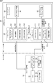
- FIG. 1 shows a control block diagram related to display control processing of a personal computer using a liquid crystal display device with a touch sensor.
- the personal computer includes an LCD module 10 and a host processing unit 14 as a host-side processing unit that controls the LCD module 10.
- the LCD module 10 includes a touch panel display 11 and driver ICs 12 and 13.
- the touch panel display 11 includes a touch panel 21 and an LCD panel 22, the driver IC 12 is a control IC (Integrated Circuit) of the touch panel 21, and the driver IC 13 is a control IC of the LCD panel 22.
- the driver IC 12 is a control IC (Integrated Circuit) of the touch panel 21
- the driver IC 13 is a control IC of the LCD panel 22.
- the driver IC 12 includes a touch panel driver 31, a detection circuit 32, and a coordinate conversion circuit 33.
- the touch panel driver 31 scans and drives the strip-shaped conductive film lines arranged in the X axis direction and the Y axis direction on the touch panel 21.
- the detection circuit 32 detects an analog sensor signal indicating a capacitance value according to the presence or absence of a user's touch (contact) at a predetermined position of the touch panel 21 according to the scanning drive of the touch panel driver 31, and outputs a digital signal Convert to AD.
- the coordinate conversion circuit 33 converts a digital sensor signal indicating the touch detection position detected by the detection circuit 32 into a two-dimensional coordinate position represented by the X coordinate position and the Y coordinate position of the touch panel 21, and as raw coordinate information, Output to the host processing unit 14.
- the driver IC 13 includes an LCD driver 41, a memory 42, and a timing controller 43.
- the driver IC 13 performs calculations such as calibration and filtering on the raw coordinate position indicating the touch position output from the driver IC 12, and display data of display information A based on the calculation result is displayed on the host processing unit 14. Supplied from
- the LCD driver 41 displays the display information A supplied from the host processing unit 14 based on the display data stored in the memory 42, so that each pixel (internal) of the LCD panel 22 arranged in a two-dimensional manner is displayed. Are driven in a predetermined order.
- the memory 42 stores display data of display information A supplied from the host processing unit 14.
- the timing controller 43 acquires the display data of the display information A supplied from the host processing unit 14 and stores it in the memory 42.
- the host processing unit 14 includes a CPU (Central Processing Unit) 51, a memory (RAM: Random Access Memory) 52, a graphics controller 53, and an image memory (VRAM) 54.
- CPU Central Processing Unit
- RAM Random Access Memory
- VRAM image memory
- the CPU 51 is a processor that controls the entire personal computer, and executes a device driver, an operating system (OS), an application program, and the like of each device mounted on the personal computer.
- the memory 52 stores data necessary for the CPU 51 to execute a predetermined process, for example, an execution program.
- the CPU 51 obtains the raw coordinate position indicating the user's touch position as the raw coordinate information from the driver IC 12 of the LCD module 10, the CPU 51 accurately calculates the user's touch position by calculating the center of gravity of the raw coordinate position, averaging, and the like. And the touch position after calibration (calibration coordinate position) is calculated.
- the graphics controller 53 is a processor for displaying an image on the LCD panel 22, and outputs the display data of the image to be displayed on the LCD panel 22 to the driver IC 13 of the LCD panel 22 while appropriately storing the display data in the image memory 54. To do.
- the graphics controller 53 outputs display data of the display information A as a display image in response to the touch position to the driver IC 13 of the LCD panel 22 based on the calibration coordinate position of the user.
- an analog sensor signal having a capacitance value indicating the touch is detected by the detection circuit 32.
- the analog sensor signal is converted into a digital sensor signal by the detection circuit 32, then converted into a two-dimensional coordinate position by the coordinate conversion circuit 33, and supplied to the CPU 51 of the host processing unit 14 as raw coordinate information.
- the CPU 51 of the host processing unit 14 performs calibration or the like on the two-dimensional coordinate position as the raw coordinate information, and calculates the calibration coordinate position corresponding to the touch position of the user. Then, display data of display information A generated based on the calculated calibration coordinate position is supplied to the driver IC 13 of the LCD panel 22 via the graphics controller 53.
- the timing controller 43 of the driver IC 13 of the LCD panel 22 acquires display data of the display information A and stores it in the memory 42, and the LCD driver 41 displays the LCD according to the display data of the display information A stored in the memory 42.
- the panel 22 is driven. As a result, the display information A is displayed on the LCD panel 22.
- the raw coordinate information indicating the detected touch position is supplied to the CPU 51, and the CPU 51 performs complicated arithmetic processing such as filtering and calibration, and then the LCD panel. 22 is displayed.
- the present technology has been made in view of such a situation, and is intended to improve the operability of the touch panel display.
- the display control device obtains first display data indicating a touch input position of the user with respect to the touch panel display from the first processing unit via the first path, and the first display.
- Second display data is acquired via a second path from a second processing unit that executes display image generation processing having a larger processing amount than the first processing unit using data, and the first display
- the display control part which performs control which displays the 1st display information based on data and the 2nd display information based on the 2nd display data on the touch panel display is provided.
- the display control method acquires first display data indicating a touch input position of the user with respect to the touch panel display from the first processing unit via the first path, and the first display.
- Second display data is acquired via a second path from a second processing unit that executes display image generation processing having a larger processing amount than the first processing unit using data, and the first display Control is performed to display the first display information based on the data and the second display information based on the second display data on the touch panel display.
- a program acquires first display data indicating a touch input position of a user with respect to a touch panel display from a first processing unit to a computer via a first path.
- Second display data is acquired via a second pass from a second processing unit that executes display image generation processing having a larger processing amount than the first processing unit using display data, and the first processing unit This is for executing a process for performing control to display the first display information based on the display data and the second display information based on the second display data on the touch panel display.
- the first display data indicating the touch input position of the user with respect to the touch panel display is acquired from the first processing unit via the first path, and the first display data is used.
- the second display data is acquired through the second path from the second processing unit that executes the display image generation process having a larger processing amount than the first processing unit, and is based on the first display data. Control for causing the touch panel display to display first display information and second display information based on the second display data is performed.
- program can be provided by being transmitted through a transmission medium or by being recorded on a recording medium.
- the display control device may be an independent device, or may be an internal block constituting one device.
- the operability of the touch panel display can be improved.
- FIG. 1 It is a control block diagram regarding the display control with respect to the conventional touch input. It is a figure explaining the structure of the touchscreen display which can apply this technique. It is a figure explaining the structure of the touchscreen display which can apply this technique. It is a block diagram which shows the structural example of 1st Embodiment of the LCD module to which this technique was applied. It is a figure which shows the example of a display with respect to the touch input using this technique. It is a figure which shows the example of a display with respect to the conventional touch input. It is a block diagram which shows the structural example of 2nd Embodiment of the LCD module to which this technique was applied. It is a block diagram which shows the structural example of 3rd Embodiment of the LCD module to which this technique was applied. FIG.
- FIG. 9 is a block diagram illustrating a detailed configuration of the driver LSI of FIG. 8. It is a figure showing a path of display control of this art. It is a flowchart explaining the display control process which does not go through via the host side processor. It is a flowchart explaining the display control process via a host side processor. It is a figure showing a path of other display control of this art.
- FIG. 20 is a block diagram of a computer to which the present technology is applied. It is a block diagram of a high-functional type mobile phone terminal to which the present technology is applied. It is a figure explaining the 1st modification of this art. It is a figure explaining the 2nd modification of this art. It is a figure explaining the 3rd modification of this art. It is a figure explaining the 4th modification of this art. It is a figure explaining the 5th modification of this art.
- the structure of the touch panel display is roughly classified into an external type and a built-in type as shown in FIG.
- the external touch panel display has a touch panel attached to the surface of the LCD panel.
- the touch panel display 11 shown in FIG. 1 includes a touch panel 21 and an LCD panel 22, and corresponds to an external type.
- the image display panel since the image display panel and the touch panel are separately configured, the image display panel may be a PDP panel, an OLED panel, or the like in addition to the LCD panel.
- the built-in touch panel display has a structure in which a touch panel function is formed inside the LCD panel, and can be further classified into an in-cell type and an on-cell type.
- the in-cell type has a built-in touch panel function in the TFT-LCD cell
- the on-cell type has a built-in touch panel function between a polarizing plate and a glass substrate provided with a color filter.
- in-cell type detection methods include a contact type using a micro switch, a capacitance type that detects a change in capacitance, an optical type that detects light, and the like. There is also a hybrid type using both.
- on-cell type detection methods include a resistance type that detects a change in resistance value (voltage value) and a capacitance type that detects a change in capacitance.
- Touch panel displays can be classified into various structures as described above, but the present technology can be applied to all structures, whether external, built-in, on-cell, or in-cell.
- an in-cell (built-in) touch panel display using a capacitive detection method is employed.
- the built-in touch panel display described below has a touch panel function formed inside the LCD panel, but this is also applicable to a panel with a touch panel function formed inside the OLED panel.
- Technology can be applied.
- Built-in touch panel display has a touch sensor function, improved visibility, higher touch discrimination area, improved S / N ratio of sensor signal, thinner display, etc. There are benefits. In particular, due to the high density of the touch area and the improvement of the S / N ratio of the sensor signal, the built-in touch panel display can be detected just by approaching the finger, enabling new operation experiences such as proximity sensing. Become.
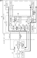
- FIG. 4 shows a block diagram of the LCD module 80 to which the present technology is applied and the host processing unit 14 that controls the LCD module 80.
- the LCD module 80 and the host processing unit 14 are configured as a part of a personal computer, for example, as in FIG.
- the LCD module 80 includes a touch panel display 81 and driver ICs 82 and 83.
- the host processing unit 14 is a host-side processing unit similar to that in FIG. 1 that controls the LCD module 80, and the description of the host processing unit 14 is omitted because it overlaps with the above description.
- the touch panel display 81 is the above-described built-in and in-cell type touch panel display that employs, for example, a capacitive detection method, and includes a touch sensor unit 91 and a display module unit 92.
- the driver IC 82 includes a touch panel driver 101, a detection circuit 102, and a coordinate conversion circuit 103, and controls the touch sensor unit 91.
- the touch sensor unit 91 detects a sensor signal detected in each region obtained by dividing the display surface of the touch panel display 81 into a plurality of regions in a two-dimensional matrix in a predetermined order by driving control of the touch panel driver 101. Output to.
- the touch panel driver 101 drives and controls the touch sensor unit 91.
- the detection circuit 102 detects (acquires) an analog sensor signal indicating a capacitance value according to the presence or absence of a user's touch at a predetermined position (each region) of the touch panel display 81 according to the drive control of the touch panel driver 101. AD conversion to a digital signal.
- the detection circuit 102 supplies a digital sensor signal to the coordinate conversion circuit 103 and also outputs it to the driver IC 83 as raster format sensor data.
- the coordinate conversion circuit 103 converts the digital sensor signal at a predetermined position detected by the detection circuit 102 into a two-dimensional coordinate position represented by the X coordinate position and the Y coordinate position of the touch panel display 81, and as raw coordinate information, Output to the host processing unit 14.
- the driver IC 83 includes an LCD driver 111, a memory 112, a timing controller 113, and a setting storage unit 114, and controls the display module unit 92.
- the LCD driver 111 drives each pixel (inner transistor) of the display module unit 92 arranged in a two-dimensional manner in a predetermined order in order to display the display information stored in the memory 112.
- the memory 112 stores display data of display information displayed on the display module unit 92.
- Display data of display information B corresponding to is stored.
- the sensor data directly supplied from the detection circuit 102 of the driver IC 82 is a digital sensor signal indicating the touch location of the user.
- the touch position is specified, but there is color information indicating what color is displayed. Not done. Therefore, the memory 112 generates display data to be drawn in the color indicated by the color information stored in the setting storage unit 114 at the display position indicated by the sensor data supplied from the detection circuit 102, and the supplied sensor data Stored as display data of corresponding display information B.
- the display information B is first display information obtained by quickly feeding back the touch position of the user detected by the touch sensor unit 91.
- the display information A supplied via the host processing unit 14 is the touch sensor unit.
- the touch position of the user detected in 91 is the second display information calibrated by the host processing unit 14.
- updating of the drawing information of the display information B based on the sensor data from the driver IC 82 and updating of the drawing information of the display information A from the graphics controller 53 of the host processing unit 14 are performed in parallel at different timing periods. Executed.
- the update of the drawing information of the display information B from the driver IC 82 does not require a complicated calculation such as calibration or filtering that is executed by the host processing unit 14, so that the drawing information update cycle of the display information A is longer than that. It is executed in a short cycle. Therefore, when a touch of the user is detected by the touch sensor unit 91, first, the display information B corresponding to the touch is drawn on the display, and then the display information that is calculated by the host processing unit 14 such as calibration. A is drawn (redrawn) on the display.
- the timing controller 113 acquires the display data of the display information A supplied from the host processing unit 14 and stores it in the memory 112.
- the setting storage unit 114 stores color information for determining a drawing color when drawing a touch position for generating display information B based on sensor data from the driver IC 82. This color information is stored in advance in the setting storage unit 114 by setting it on a predetermined application executed by the CPU 51, for example.
- the LCD driver 111 acquires the sensor data from the driver IC 82 and generates the display information B, and directly displays it in the display module unit 92. You may draw.
- FIG. 5 shows a display example in which the host processing unit 14 and the LCD module 80 of FIG.
- the sensor data of the touch position X1 is supplied from the driver IC 82 to the driver IC 83 at the moment when the user touches. Then, the driver IC 83 draws (displays) the point B1 at the same position as the position X1 touched by the user as the display information B1 at the time t1.
- the raw coordinate information of the touch position X1 is supplied to the host processing unit 14, and the host processing unit 14 performs a calibration calculation and the like, and supplies it to the driver IC 83 as display data of the display information A1. Then, at the time t2 when the user touches the position X2 on the left side of the position X1 after the elapse of a predetermined time from the time t1, the display data of the display information A1 is displayed together with the point B2 drawn as the display information B2 at the position X2. A base point A1 is drawn at position X1. That is, the point A1 (display information A1) generated via the host processing unit 14 is displayed at the time t2 when the position X2 is touched with a delay from the time t1.
- the point B3 as the display information B3 is drawn at the position X3 touched by the user, and the point A2 generated by the host processing unit 14 and displayed with a delay is displayed at the position X2. Drawn.
- a point B4 as display information B4 is drawn at a position X4 touched by the user, and a point A3 generated by the host processing unit 14 and displayed with a delay is drawn at the position X3. .
- FIG. 6 shows a display example when similar touch and slide operations are drawn by a conventional display control method.
- the point A1 is drawn at the position X1 at a time t2 delayed by a predetermined time from the time t1, but as described above, at the time t2, the user slides the finger position and the user's finger moves to the position X2. is doing.
- the point A2 is drawn at the position X2 touched at the time t2 slightly before that
- the time t4 when the user touches the position X4
- a point A3 is drawn at the position X3 touched at time t3 slightly before that.
- the driver IC 82 does not pass through the host processing unit 14.
- Display information B is drawn based on the sensor data directly supplied to the driver IC 83.
- the display control of the LCD module 80 to which the present technology is applied it is possible to provide quick feedback to the touch input of the user, and the operability derived from the drawing delay via the host processing unit 14. The decrease can be suppressed. That is, the operability of the touch panel display can be improved.
- FIG. 7 shows a block diagram of the LCD module 80 of the second embodiment and the host processing unit 14 that controls it.
- the LCD module 80 of the second embodiment is different from the first embodiment shown in FIG. 4 in that a coordinate correction circuit 104 is newly added to the driver IC 82.
- the two-dimensional coordinate position of the touch panel display 81 touched by the user is output to the host processing unit 14 as raw coordinate information, and the host processing unit 14 uses the average value and standard deviation of the raw coordinate position. Calibration was performed to accurately calculate the user's touch position by performing the correction calculation.
- the coordinate correction circuit 104 performs calibration for calculating the accurate touch position of the user based on the raw coordinate information, which is performed by the host processing unit 14 in the first embodiment described above. Do.
- the coordinate correction circuit 104 outputs a correction coordinate value indicating the touch position of the user after the correction calculation to the host processing unit 14 and the driver IC 83 as correction coordinate information.
- the configuration of the second embodiment is useful when the storage device on the host side that stores the correction data for calibration is write-protected or the connected host side is unspecified.
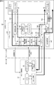
- FIG. 8 shows a block diagram of the LCD module 80 according to the third embodiment and the host processing unit 14 that controls the LCD module 80.
- one driver LSI (Large Scale Integration) 121 is configured by two driver ICs of the driver IC 82 and the driver IC 83 in the first and second embodiments. The other points are the same.
- the driver LSI 121 is formed on a single semiconductor substrate using single crystal silicon by, for example, a known complementary MOS integrated circuit manufacturing technique.
- the configuration in which the coordinate correction circuit 104 is omitted corresponds to the first embodiment in FIG. 4, and the configuration in which the coordinate correction circuit 104 is added corresponds to the second embodiment in FIG.
- FIG. 9 is a functional block diagram illustrating the driver LSI 121 according to the third embodiment in further detail. The display control using the driver LSI 121 will be further described with reference to FIG.
- the driver LSI 121 includes at least an AD conversion circuit 141, a capacitance value storage register 142, a rasterizer 143, a frame memory 146, a coordinate conversion circuit 144, a system interface 145, a setting storage unit 147, and a display data generation unit 148.
- the AD conversion circuit 141, the capacitance value storage register 142, and the rasterizer 143 correspond to the function of the detection circuit 102 in FIG.
- the coordinate conversion circuit 144, the system interface 145, the frame memory 146, the setting storage unit 147, and the display data generation unit 148 are respectively the coordinate conversion circuit 103, the timing controller 113, the memory 112, the setting storage unit 114, FIG. And the LCD driver 111.
- the average value calculation unit 151, the standard deviation calculation unit 152, and the hysteresis calculation unit 153 correspond to the coordinate correction circuit 104 in FIG.
- the AD conversion circuit 141 detects an analog sensor signal from the touch sensor unit 91, performs AD conversion to a digital sensor signal, and supplies the digital sensor signal to the capacitance value storage register 142 and the average value calculation unit 151.
- the digital sensor signal is supplied to the coordinate conversion circuit 144 instead of the average value calculation unit 151.
- the capacitance value storage register 142 stores a digital capacitance value that is a sensor signal supplied from the AD conversion circuit 141.
- the rasterizer 143 converts (rasterizes) the digital capacitance value stored in the capacitance value storage register 142 into a raster format, and stores it in the frame memory 146.
- the coordinate conversion circuit 144 calculates the two-dimensional coordinate position on the display touched by the user based on the digital capacitance value as the sensor signal supplied from the AD conversion circuit 141.
- the system interface 145 outputs the two-dimensional coordinate position indicating the touch position of the user supplied from the coordinate conversion circuit 144 to the host processing unit 14 such as a personal computer via a system bus (not shown).
- the system interface 145 stores various control information supplied from the host processing unit 14 in an internal register (not shown) in the driver LSI 121.
- system interface 145 acquires display data to be displayed on the display of the display module unit 92 supplied from the host processing unit 14 and stores it in the frame memory 146.
- the frame memory 146 has a storage capacity capable of holding display data for one screen.
- the frame memory 146 stores the supplied display data by overwriting the currently held display data. Display data held in the frame memory 146 is read by the display data generation unit 148 at an optimal timing.
- the digital capacitance value supplied from the rasterizer 143 is converted into display data B of display information B representing the touch position in a predetermined color based on the setting information stored in the setting storage unit 147, and the frame Stored in the memory 146.
- the system interface 145 is supplied with display data of display information A generated by the CPU 51 of the host processing unit 14 performing a calibration calculation or the like on the two-dimensional coordinate position indicating the touch position of the user, and the frame memory 146.
- the setting storage unit 147 stores setting information that defines the drawing color when the touch position on the display is displayed as the display information B.
- the display data generation unit 148 reads the display data stored in the frame memory 146 and applies a voltage corresponding to the display data to the drain line (data line) of the display module unit 92, thereby Each pixel (inner transistor) is driven. As a result, an image (display information) corresponding to the display data stored in the frame memory 146 is displayed on the display of the display module unit 92.
- the average value calculation unit 151, the standard deviation calculation unit 152, and the hysteresis calculation unit 153 are provided, the average, standard deviation, and hysteresis of each capacitance value indicating the user's touch are calculated.
- a corrected coordinate value obtained by accurately correcting the touch position is calculated and supplied to the coordinate conversion circuit 144.
- the sensor signal detected by the touch sensor unit 91 is displayed as display information B by the path 162 indicated by the thick broken line in FIG.
- display information A is displayed on the display through a path 161 indicated by a solid line in FIG.
- a thick solid line path 161 is a path that passes through the CPU 51 and the graphics controller 53 of the host processing unit 14, and a thick broken line path 162 is processed in the driver LSI 121 without going through the host processing unit 14. Pass.
- the thick solid-line path 161 is a path with a large amount of processing (calculation amount) for generating display information for performing a calibration calculation or the like on the sensor signal detected by the touch sensor unit 91.
- a thick broken line path 162 is a path with a small amount of processing (calculation amount) for generating display information from a sensor signal detected by the touch sensor unit 91.
- the display information B generated by the path 162 that does not pass through the host-side processor is drawn. Delay time until rendering can be suppressed.
- Display control processing for display information B> A display control process for displaying the display information B corresponding to the user's touch input on the display of the display module unit 92 through the path 162 that does not pass through the host side processor will be described with reference to the flowchart of FIG.
- step S ⁇ b> 1 the AD conversion circuit 141 detects an analog sensor signal indicating the capacitance value from the touch sensor unit 91, converts it to a digital signal, and supplies it to the capacitance value storage register 142.
- the capacitance value storage register 142 stores the digital sensor signal indicating the capacitance value supplied from the AD conversion circuit 141.
- step S 2 the rasterizer 143 converts the digital capacitance value stored in the capacitance value storage register 142 into a raster format and stores it in the frame memory 146.
- the digital capacitance value supplied from the rasterizer 143 is converted into display data B of display information B representing the touch position in a predetermined color based on the setting information stored in the setting storage unit 147, and the frame Stored in the memory 146.
- step S3 the display data generation unit 148 reads the display data stored in the frame memory 146, and drives each pixel (inner transistor) of the display module unit 92.
- a predetermined position on the display touched by the user in the display image displayed on the display of the display module unit 92 is displayed as display information B in a predetermined color.
- step S ⁇ b> 11 the AD conversion circuit 141 detects an analog sensor signal indicating a capacitance value from the touch sensor unit 91, performs AD conversion to a digital signal, and supplies the digital signal to the coordinate conversion circuit 144.
- the process of step S11 is executed as one process together with the process of step S1 of FIG.
- the average value calculation unit 151 or the like When performing a calibration calculation, the average value calculation unit 151 or the like performs a calibration calculation on the sensor signal from the AD conversion circuit 141, and the sensor signal after the calibration calculation is supplied to the coordinate conversion circuit 144. Is done.
- step S12 the coordinate conversion circuit 144 calculates the two-dimensional coordinate position on the display touched by the user based on the digital capacitance value as the sensor signal supplied from the AD conversion circuit 141.
- step S13 the system interface 145 outputs the two-dimensional coordinate position indicating the touch position of the user supplied from the coordinate conversion circuit 144 to the host processing unit 14 via a system bus (not shown).
- step S ⁇ b> 14 the system interface 145 obtains display data of display information A generated by performing an operation such as calibration on the two-dimensional coordinate position indicating the touch position of the user supplied to the host processing unit 14. And stored in the frame memory 146.
- step S15 the display data generation unit 148 reads the display data stored in the frame memory 146, and drives each pixel (inner transistor) of the display module unit 92.
- the process in step S15 and the process in step S3 described above are the same single process.
- the predetermined position on the display touched by the user is displayed in the predetermined color as the display information A by the display control of the CPU 51 and the graphics controller 53 on the host side.
- the display control process for displaying the display information B through the path 162 that does not pass through the host-side processor described with reference to FIG. 11 is further executed.
- the display control process by the path 162 is a process that does not go through the host side processor, the display control process by the path 161 can be immediately displayed for the touch detection earlier than the display control process by the path 161. Thereby, the time difference from the user's touch detection to drawing (display) on the display can be shortened, and the drawing delay felt by the user can be reduced.
- the path that does not pass through the host-side processor may be the path 163 indicated by a thick broken line in FIG. 13 in addition to the path 162 described above. That is, a two-dimensional coordinate value obtained from an AD converted digital sensor signal may be generated and displayed as display data of the display information B.
- Example of personal computer configuration> The present technology can be applied to an electronic device having a built-in touch panel display, such as a computer, a mobile phone terminal, a tablet terminal, a portable game machine, and a portable music video playback device.
- 14 and 15 show the overall configuration of a computer and a mobile phone.
- FIG. 14 is a block diagram of a computer (personal computer) including the LCD module 80 to which the present technology is applied and the host processing unit 14 that controls the LCD module 80.
- the CPU 201 controls the entire computer system according to various programs.
- the ROM 202 stores a boot program used by the CPU 201, calculation parameters, and the like.
- the RAM 203 temporarily stores programs used in the execution of the CPU 201, parameters that change as appropriate during the execution, and the like.
- the computer also has an interface (such as a keyboard 204 for inputting characters, numerical values, various instructions, etc., a mouse 205 for moving a cursor, selecting a range, and the like, an external device such as a controller, a scanner, and a printer ( I / F) 206.
- an interface such as a keyboard 204 for inputting characters, numerical values, various instructions, etc.
- a mouse 205 for moving a cursor, selecting a range, and the like
- an external device such as a controller, a scanner, and a printer ( I / F) 206.
- the keyboard 204 and the mouse 205 are omitted.
- the computer further includes a graphic board 207 for controlling image display, a network device for connecting to a network, a communication device 208 including a modem, a display 209 having a touch panel function, and a hard disk 210 as a data storage device.
- a graphic board 207 for controlling image display
- a network device for connecting to a network
- a communication device 208 including a modem
- a display 209 having a touch panel function
- a hard disk 210 as a data storage device.
- the hard disk 210 stores an operating system (OS), device drivers for various devices, and various application programs such as a word processor and spreadsheet software.
- OS operating system
- application programs such as a word processor and spreadsheet software.
- the graphics controller 53 and the image memory 54 in FIG. 4 are arranged in the graphic board 207 in FIG. 14, and the LCD module 80 corresponds to the display 209 in FIG.
- FIG. 15 is a block diagram of a high-function mobile phone terminal (smart phone) including the LCD module 80 to which the present technology is applied and the host processing unit 14 that controls the LCD module 80.
- a communication antenna 221 is, for example, a built-in antenna, and is used to download and transmit various application programs including an information input control program based on the touch detection described above, transmission and reception of calls and e-mails via a mobile phone network and a public wireless communication network, Transmits and receives signal radio waves for communication with the Internet.
- the antenna circuit 222 includes an antenna switch, a matching circuit, a filter circuit, and the like, and the transmission / reception circuit unit 223 performs frequency conversion, modulation, demodulation, and the like of transmission / reception signals through a mobile phone network or a public wireless communication network.
- the speaker 236 is used, for example, for music reproduction, reception sound output, ringer sound (ringing tone) output, and the like.
- the microphone 237 is used for collecting external sound, collecting transmitted sound, and the like.
- the audio signal processing unit 235 includes an amplification circuit for the speaker 236, an amplification circuit for the microphone 237, a decompression decoding circuit that decompresses and decodes the compressed and encoded audio data supplied from the control / arithmetic unit 224, and the decompression decoding.
- Digital / analog conversion circuit for converting the converted digital audio data into an analog audio signal
- an analog / digital conversion circuit for converting the analog audio signal input from the microphone 237 into digital audio data
- compression encoding the digital audio data It consists of a compression encoding circuit.
- the video signal processing unit 231 expands and decodes the compression-encoded video data supplied from the control / arithmetic unit 224, and outputs the decompressed and decoded digital video and a digital broadcast receiving module 229 described later.
- the display panel drive circuit or the like for displaying the received digital broadcast video on the touch panel display 233.
- the video signal processing unit 231 also generates display data for displaying a desktop image and various menu images supplied from the control / calculation unit 224, a virtual touch area image corresponding to a position on the touch panel display 233, and the like. Those images are displayed on the touch panel display 233.
- the touch panel display 233 has a touch sensor unit that can detect an input operation by the user.
- the touch panel signal processing unit 232 measures the touch detection position, touch locus, touch duration, touch time interval, and the like from the touch panel display 233, and sends the measured data to the control / calculation unit 224 as touch detection data.
- the touch input to the display surface of the touch panel display 233 can be performed by a stylus attached to the terminal in addition to the user's finger or the like.
- the touch panel display 233 and the touch panel signal processing unit 232 support so-called multi-touch.
- the key operation unit 240 includes a hard key provided on the casing of the mobile phone terminal and its peripheral circuit.
- the key operation unit 240 converts a hard key press operation by the user into an electrical signal, amplifies and analog / digital converts the operation input signal, and sends the operation input data after the analog / digital conversion to the control / calculation unit 224. send.
- the external input / output terminal unit 239 includes, for example, a cable connection connector and an external data communication interface circuit when performing data communication through a cable, a charging terminal and its charging interface circuit when charging an internal battery through a power cable, etc. Consists of.
- the external memory I / F unit 230 includes an external memory slot to which a storage medium such as an external memory is attached and detached, and an external memory data communication interface circuit.
- the near field communication module 228 includes a communication antenna for near field radio waves such as a wireless LAN and Bluetooth (registered trademark), and a near field communication circuit.
- the digital broadcast receiving module 229 includes a receiving antenna and a tuner for so-called digital television broadcasting and digital radio broadcasting.
- the digital broadcast receiving module 229 can receive not only single-channel digital broadcasts but also multiple-channel digital broadcasts at the same time.
- the digital broadcast receiving module 229 can also receive data multiplexed in the digital broadcast.
- the digital broadcast data received by the digital broadcast receiving module 229 can be stored (that is, recorded) in the memory unit 225 after being compressed by the control / arithmetic unit 224, for example.
- the camera unit 234 includes an image sensor for photographing a still image or a moving image, an optical system, and its peripheral circuits, a light driving circuit for emitting photographing auxiliary light, and the like. Still image data and moving image data at the time of shooting by the camera unit 234 are sent to the video signal processing unit 231 as preview video data. Thereby, a preview image is displayed on the touch panel display 233 when the camera is photographed.
- the captured still image data or moving image data is sent to the control / arithmetic unit 224, compressed, and then stored in the memory. Stored in a storage medium connected to the unit 225 and the external memory I / F unit 230.
- the non-contact communication module 227 performs non-contact communication used in, for example, a so-called RFID (Radio Frequency-Identification), a non-contact type IC card, or the like through a non-contact communication antenna.
- RFID Radio Frequency-Identification
- the GPS (Global Positioning System) module 226 has a GPS antenna and obtains the latitude and longitude of the current position of the terminal using GPS signals from GPS geodetic satellites. GPS data (information indicating latitude and longitude) obtained by the GPS module 226 is sent to the control / calculation unit 224. As a result, the control / calculation unit 224 can know the current position and movement of the terminal itself.
- the various sensor units 238 include various detection sensors such as a terminal state detection sensor for detecting the state of the mobile phone terminal and its peripheral circuits.
- Examples of the various sensor units 238 include an inclination sensor, an acceleration sensor, an orientation sensor, a temperature sensor, a humidity sensor, and an illuminance sensor.
- Detection signals from the various sensor units 238 are sent to the control / calculation unit 224. Thereby, the control / calculation unit 224 can know the state (tilt, acceleration, direction, temperature, humidity, illuminance, etc.) of the mobile phone terminal.
- the memory unit 225 includes a built-in memory provided in the terminal and a removable card memory. Examples of the removable card-like memory include cards that store so-called SIM (Subscriber Identity) Module information and the like.
- the built-in memory consists of ROM (Read Only Memory) and RAM (Random Access Memory).
- the ROM stores an OS (Operating System), a control program for the control / calculation unit 224 to control each unit, various initial setting values, dictionary data, character prediction conversion dictionary data, various sound data, various application programs, and the like. ing.
- This ROM includes rewritable ROM such as NAND-type flash memory (NAND-type flash memory) or EEPROM (Electrically-Erasable Programmable Read-Only Memory), e-mail data, phone book and mail address book data, static Data of image and moving image content, and other various user setting values can be stored.
- the RAM stores data as needed as a work area and a buffer area when the control / arithmetic unit 224 performs various data processing.
- the control / arithmetic unit 224 includes a CPU (central processing unit), and includes a transmission / reception circuit unit 223, a video signal processing unit 231, an audio signal processing unit 235, a GPS module 226, a non-contact communication module 227, a short-range wireless communication module 228, Controls each part such as a digital broadcast receiving module 229, an external memory I / F part 230, a camera part 234, various sensor parts 238, an external input / output terminal part 239, a key operation part 240, a touch panel signal processing part 232, and the like. Perform various calculations.
- the control / arithmetic unit 224 executes a control program and various application programs stored in the memory unit 225.
- the cellular phone terminal is naturally also about each component provided in a general cellular phone terminal, such as a clock unit that measures time and time, a battery that supplies power to each unit, and a power management IC that controls the power. I have.
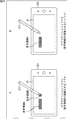
- FIG. 16 shows a display example of the touch panel display 81 corresponding to the first modification.
- the driver IC 83 When the touch of the user is detected on the touch panel display 81 and sensor data corresponding to the touch position is supplied from the detection circuit 102 of the driver IC 82 to the driver IC 83, the driver IC 83 responds to the color (background color) of the display image. Then, the drawing color of the display information B is automatically determined (changed), and the display information B is drawn. For example, the driver IC 83 determines and draws a color (complementary color) contrasting with the background color as the drawing color of the display information B.
- 16A shows an example in which, when a white background image is displayed on the touch panel display 81 of the mobile phone terminal 301, the driver IC 83 draws the touch position touched by the user with the stylus 311 in black as the display information B. Is shown.
- FIG. 16B illustrates an example in which, when a black background image is displayed on the touch panel display 81 of the mobile phone terminal 301, the driver IC 83 draws the touch position touched by the user with the stylus 311 in white as the display information B. Is shown.
- FIG. 17 shows a display example of the touch panel display 81 corresponding to the second modification.
- the second modification is an example in which the display information B is drawn with the set color and size in advance when the display information B is drawn in color and size.
- FIG. 17A shows an example of a setting screen for setting the color and size when the display information B is drawn.
- a setting screen as shown in FIG. 17A is displayed on the touch panel display 81, and the user selects the color and size when the display information B is drawn.
- the color and size selected by the user are stored in the setting storage unit 114 as setting information. Note that in the setting screen of A in FIG. 17, the difference in color of the display information B is represented by the difference in pattern (pattern).
- the driver IC 83 uses the color and size indicated by the setting information stored in the setting storage unit 114.
- Draw display information B the display information B can be drawn with an arbitrary color and size selected by the user.
- FIG. 18 shows a display example of the touch panel display 81 corresponding to the third modification.
- the set color or size is set. This is an example of drawing display information B using
- FIG. 18A shows an example of a setting screen for setting the color and size when drawing characters and pictures in an application for drawing characters and pictures. Since the color and size set here are reflected in the display image generated by the application executed by the CPU 51 of the host processing unit 14, it corresponds to the color and size of the display information A via the host-side processor. To do.
- the driver IC 83 is the same as the drawing color and size of the display information A.
- Draw display information B with color and size. Thereby, the display color B of the display information B drawn through the host side processor and the display information A drawn through the host side processor are the same.
- the display information B is drawn on the touch panel display 81 first, and then the display information A is displayed on the display information B. Rendered in a replacement form.
- the display information A may be instantaneously replaced, but the display information A is changed from the display information B by gradually changing the transmittance when the display information A is superimposed on the display information B.
- the display may be controlled so as to be gradually replaced.
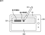
- FIG. 19 shows a display example of the touch panel display 81 corresponding to the fourth modification.
- the fourth modification example only the display information A and the display information A are drawn in the touch input area of the touch panel display 81 by drawing the display information A and the display information B. It is an example which divides the area
- the driver IC 83 uses the display information B generated without going through the host side processor and the host side processor. Both display information A to be generated is drawn. On the other hand, in the area 322 other than the area 321, only the display information A via the host side processor is drawn.
- FIG. 20 shows a display example of the touch panel display 81 corresponding to the fifth modification.
- the fifth modified example is an example in which display information A and display information B are drawn, and whether or not to provide quick feedback with respect to a user's touch input is distinguished depending on the application.
- the driver IC 83 draws the display information A and the display information B in the application software ⁇ as shown in A of FIG. 20, but the host side processor is used in the application software ⁇ as shown in B of FIG. Only the display information A that has passed is drawn.
- the driver IC 83 can switch whether or not to draw the display information B by acquiring, from the application software, a flag indicating whether or not to enable drawing of the display information B that does not pass through the host-side processor.
- Embodiments of the present technology are not limited to the above-described embodiments, and various modifications can be made without departing from the gist of the present technology.
- each step described in the above-described flowchart can be executed by one device or can be shared by a plurality of devices. Further, when a plurality of processes are included in one step, the plurality of processes included in the one step can be executed by being shared by a plurality of apparatuses in addition to being executed by one apparatus.
- First display data indicating the touch input position of the user with respect to the touch panel display is acquired from the first processing unit via the first path, and from the first processing unit using the first display data.
- Second display data is acquired via a second pass from a second processing unit that executes a display image generation process with a large amount of processing, and first display information based on the first display data;
- a display control apparatus comprising: a display control unit that performs control to display second display information based on second display data on the touch panel display.
- a setting storage unit for storing a drawing color when displaying the first display information using the first display data; The display control device according to (1), wherein the display control unit displays the first display information in a drawing color set in the setting storage unit.
- a setting unit configured to set a drawing color when displaying the first display information using the first display data;
- the display control device according to (1) or (2), wherein the setting storage unit stores the drawing color set by the setting unit.
- the display control unit determines a drawing color of the first display information according to a background color of a display image displayed on the touch panel display, and causes the display color to be displayed. Any one of (1) to (3) The display control apparatus described.
- the display control according to any one of (1) to (4), wherein the display control unit determines and displays a drawing setting of the first display information according to a drawing setting of the second display information. apparatus.
- the display control unit replaces the first display information with the second display information by gradually changing the transmittance of the first display information and the second display information.
- the display control device according to any one of (5). (7) The display control unit distinguishes between a case where both the first display information and the second display information are displayed and a case where only the second display information is displayed according to a display area of the touch panel display. The display control device according to any one of (1) to (6). (8) The display control unit distinguishes between a case where both the first display information and the second display information are displayed and a case where only the second display information is displayed, depending on the application. 7) The display control apparatus in any one of. (9) The display control device according to any one of (1) to (8), wherein the first display data is sensor data of the touch input position.
- the display control device according to any one of (1) to (9), wherein the first display data is data after a calibration calculation is performed on sensor data at the touch input position.
- First display data indicating the touch input position of the user with respect to the touch panel display is acquired from the first processing unit via the first path, and from the first processing unit using the first display data.
- Second display data is acquired via a second pass from a second processing unit that executes a display image generation process with a large amount of processing, and first display information based on the first display data;
Abstract
Description
1.本技術が適用されるタッチパネルの構造の説明
2.LCDモジュールの第1の実施の形態
3.LCDモジュールの第2の実施の形態
4.LCDモジュールの第3の実施の形態
5.パーソナルコンピュータの構成例
6.携帯電話端末の構成例
7.変形例 Hereinafter, modes for carrying out the present technology (hereinafter referred to as embodiments) will be described. The description will be given in the following order.
1. 1. Description of touch panel structure to which the present technology is applied 1. First embodiment of LCD module 2. Second embodiment of LCD module 4. Third embodiment of LCD module 5. Configuration example of personal computer 6. Configuration example of mobile phone terminal Modified example
初めに、図2および図3を参照して、以下に後述する本技術が適用可能なタッチパネルディスプレイの構造について説明する。 <1. Explanation of touch panel structure to which this technology is applied>
First, the structure of a touch panel display to which the present technology described below can be applied will be described with reference to FIGS. 2 and 3.
本技術が適用されたLCDモジュールの第1の実施の形態について説明する。 <2. First Embodiment of LCD Module>
A first embodiment of an LCD module to which the present technology is applied will be described.
図5は、図4のホスト処理部14とLCDモジュール80により、ユーザがタッチしたディスプレイ上の位置を、点で描画する表示例を示している。 <Display example for user touch input>
FIG. 5 shows a display example in which the
次に、LCDモジュールの第2の実施の形態について説明する。 <3. Second Embodiment of LCD Module>
Next, a second embodiment of the LCD module will be described.
次に、LCDモジュールの第3の実施の形態について説明する。 <4. Third Embodiment of LCD Module>
Next, a third embodiment of the LCD module will be described.
図11のフローチャートを参照して、ホスト側プロセッサを経由しないパス162により、ユーザのタッチ入力に対応する表示情報Bをディスプレイモジュール部92のディスプレイに表示させる表示制御処理について説明する。 <Display control processing for display information B>
A display control process for displaying the display information B corresponding to the user's touch input on the display of the
次に、図12のフローチャートを参照して、ホスト側プロセッサを経由するパス161により、ユーザのタッチに対応する表示情報Aをディスプレイモジュール部92のディスプレイに表示させる表示制御処理について説明する。 <Display control processing for display information A>
Next, a display control process for displaying the display information A corresponding to the user's touch on the display of the
本技術は、例えば、コンピュータ、携帯電話端末、タブレット端末、携帯用ゲーム機、携帯用音楽映像再生装置などの、内蔵型のタッチパネルディスプレイを有する電子機器に適用することができる。図14と図15で、コンピュータと携帯電話機の全体構成について示す。 <5. Example of personal computer configuration>
The present technology can be applied to an electronic device having a built-in touch panel display, such as a computer, a mobile phone terminal, a tablet terminal, a portable game machine, and a portable music video playback device. 14 and 15 show the overall configuration of a computer and a mobile phone.
図15は、本技術が適用されたLCDモジュール80と、それを制御するホスト処理部14を含む高機能型の携帯電話端末(スマートフォン)のブロック図である。 <6. Configuration example of mobile phone terminal>
FIG. 15 is a block diagram of a high-function mobile phone terminal (smart phone) including the
<第1の変形例>
上述した実施の形態では、タッチパネルディスプレイ81においてユーザのタッチが検出されたとき、ホスト側プロセッサを経由した表示情報Aを表示する前に、ホスト側プロセッサを介さずにLCDモジュール80内で処理した表示情報Bを表示させる例について説明した。以下では、ホスト側プロセッサを介さずにLCDモジュール80内で表示情報Bを表示させる場合の変形例(応用例)について説明する。 <7. Modification>
<First Modification>
In the above-described embodiment, when the touch of the user is detected on the
図17は、第2の変形例に対応するタッチパネルディスプレイ81の表示例を示している。 <Second Modification>
FIG. 17 shows a display example of the
図18は、第3の変形例に対応するタッチパネルディスプレイ81の表示例を示している。 <Third Modification>
FIG. 18 shows a display example of the
図19は、第4の変形例に対応するタッチパネルディスプレイ81の表示例を示している。 <Fourth Modification>
FIG. 19 shows a display example of the
図20は、第5の変形例に対応するタッチパネルディスプレイ81の表示例を示している。 <Fifth Modification>
FIG. 20 shows a display example of the
(1)
タッチパネルディスプレイに対するユーザのタッチ入力位置を示す第1の表示データを、第1の処理部から第1のパスを介して取得するとともに、前記第1の表示データを用いて前記第1の処理部より処理量の多い表示画像生成処理を実行する第2の処理部から、第2のパスを介して第2の表示データを取得し、前記第1の表示データに基づく第1の表示情報と、前記第2の表示データに基づく第2の表示情報を前記タッチパネルディスプレイに表示させる制御を行う表示制御部
を備える表示制御装置。
(2)
前記第1の表示データを用いて前記第1の表示情報を表示する際の描画色を記憶する設定記憶部をさらに備え、
前記表示制御部は、前記設定記憶部に設定されている描画色で、前記第1の表示情報を表示させる
前記(1)に記載の表示制御装置。
(3)
前記第1の表示データを用いて前記第1の表示情報を表示する際の描画色を設定する設定部をさらに備え、
前記設定記憶部は、前記設定部で設定された前記描画色を記憶する
前記(1)または(2)に記載の表示制御装置。
(4)
前記表示制御部は、前記タッチパネルディスプレイに表示している表示画像の背景色に応じて、前記第1の表示情報の描画色を決定し、表示させる
前記(1)乃至(3)のいずれかに記載の表示制御装置。
(5)
前記表示制御部は、前記第2の表示情報の描画設定に応じて、前記第1の表示情報の描画設定を決定し、表示させる
前記(1)乃至(4)のいずれかに記載の表示制御装置。
(6)
前記表示制御部は、前記第1の表示情報と前記第2の表示情報の透過率を徐々に変化させることにより、前記第1の表示情報を前記第2の表示情報に置き換える
前記(1)乃至(5)のいずれかに記載の表示制御装置。
(7)
前記表示制御部は、前記第1の表示情報と前記第2の表示情報の両方を表示させる場合と、前記第2の表示情報のみを表示させる場合を、前記タッチパネルディスプレイの表示領域によって区別する
前記(1)乃至(6)のいずれかに記載の表示制御装置。
(8)
前記表示制御部は、前記第1の表示情報と前記第2の表示情報の両方を表示させる場合と、前記第2の表示情報のみを表示させる場合を、アプリケーションによって区別する
前記(1)乃至(7)のいずれかに記載の表示制御装置。
(9)
前記第1の表示データは、前記タッチ入力位置のセンサデータである
前記(1)乃至(8)のいずれかに記載の表示制御装置。
(10)
前記第1の表示データは、前記タッチ入力位置のセンサデータに対してキャリブレーション演算した後のデータである
前記(1)乃至(9)のいずれかに記載の表示制御装置。
(11)
前記タッチパネルディスプレイと、
音声の集音を行うマイクロホンと、
音声出力を行うスピーカと
をさらに備える
前記(1)乃至(10)のいずれかに記載の表示制御装置。
(12)
タッチパネルディスプレイに対するユーザのタッチ入力位置を示す第1の表示データを、第1の処理部から第1のパスを介して取得するとともに、前記第1の表示データを用いて前記第1の処理部より処理量の多い表示画像生成処理を実行する第2の処理部から、第2のパスを介して第2の表示データを取得し、前記第1の表示データに基づく第1の表示情報と、前記第2の表示データに基づく第2の表示情報を前記タッチパネルディスプレイに表示させる制御を行う
表示制御方法。
(13)
コンピュータに、
タッチパネルディスプレイに対するユーザのタッチ入力位置を示す第1の表示データを、第1の処理部から第1のパスを介して取得するとともに、前記第1の表示データを用いて前記第1の処理部より処理量の多い表示画像生成処理を実行する第2の処理部から、第2のパスを介して第2の表示データを取得し、前記第1の表示データに基づく第1の表示情報と、前記第2の表示データに基づく第2の表示情報を前記タッチパネルディスプレイに表示させる制御を行う
処理を実行させるためのプログラム。 In addition, this technique can also take the following structures.
(1)
First display data indicating the touch input position of the user with respect to the touch panel display is acquired from the first processing unit via the first path, and from the first processing unit using the first display data. Second display data is acquired via a second pass from a second processing unit that executes a display image generation process with a large amount of processing, and first display information based on the first display data; A display control apparatus comprising: a display control unit that performs control to display second display information based on second display data on the touch panel display.
(2)
A setting storage unit for storing a drawing color when displaying the first display information using the first display data;
The display control device according to (1), wherein the display control unit displays the first display information in a drawing color set in the setting storage unit.
(3)
A setting unit configured to set a drawing color when displaying the first display information using the first display data;
The display control device according to (1) or (2), wherein the setting storage unit stores the drawing color set by the setting unit.
(4)
The display control unit determines a drawing color of the first display information according to a background color of a display image displayed on the touch panel display, and causes the display color to be displayed. Any one of (1) to (3) The display control apparatus described.
(5)
The display control according to any one of (1) to (4), wherein the display control unit determines and displays a drawing setting of the first display information according to a drawing setting of the second display information. apparatus.
(6)
The display control unit replaces the first display information with the second display information by gradually changing the transmittance of the first display information and the second display information. The display control device according to any one of (5).
(7)
The display control unit distinguishes between a case where both the first display information and the second display information are displayed and a case where only the second display information is displayed according to a display area of the touch panel display. The display control device according to any one of (1) to (6).
(8)
The display control unit distinguishes between a case where both the first display information and the second display information are displayed and a case where only the second display information is displayed, depending on the application. 7) The display control apparatus in any one of.
(9)
The display control device according to any one of (1) to (8), wherein the first display data is sensor data of the touch input position.
(10)
The display control device according to any one of (1) to (9), wherein the first display data is data after a calibration calculation is performed on sensor data at the touch input position.
(11)
The touch panel display;
A microphone that collects audio,
The display control device according to any one of (1) to (10), further including: a speaker that outputs sound.
(12)
First display data indicating the touch input position of the user with respect to the touch panel display is acquired from the first processing unit via the first path, and from the first processing unit using the first display data. Second display data is acquired via a second pass from a second processing unit that executes a display image generation process with a large amount of processing, and first display information based on the first display data; A display control method for performing control to display second display information based on second display data on the touch panel display.
(13)
On the computer,
First display data indicating the touch input position of the user with respect to the touch panel display is acquired from the first processing unit via the first path, and from the first processing unit using the first display data. Second display data is acquired via a second pass from a second processing unit that executes a display image generation process with a large amount of processing, and first display information based on the first display data; A program for executing processing for performing control to display second display information based on second display data on the touch panel display.
Claims (13)
- タッチパネルディスプレイに対するユーザのタッチ入力位置を示す第1の表示データを、第1の処理部から第1のパスを介して取得するとともに、前記第1の表示データを用いて前記第1の処理部より処理量の多い表示画像生成処理を実行する第2の処理部から、第2のパスを介して第2の表示データを取得し、前記第1の表示データに基づく第1の表示情報と、前記第2の表示データに基づく第2の表示情報を前記タッチパネルディスプレイに表示させる制御を行う表示制御部
を備える表示制御装置。 First display data indicating the touch input position of the user with respect to the touch panel display is acquired from the first processing unit via the first path, and from the first processing unit using the first display data. Second display data is acquired via a second pass from a second processing unit that executes a display image generation process with a large amount of processing, and first display information based on the first display data; A display control apparatus comprising: a display control unit that performs control to display second display information based on second display data on the touch panel display. - 前記第1の表示データを用いて前記第1の表示情報を表示する際の描画色を記憶する設定記憶部をさらに備え、
前記表示制御部は、前記設定記憶部に設定されている描画色で、前記第1の表示情報を表示させる
請求項1に記載の表示制御装置。 A setting storage unit for storing a drawing color when displaying the first display information using the first display data;
The display control apparatus according to claim 1, wherein the display control unit displays the first display information in a drawing color set in the setting storage unit. - 前記第1の表示データを用いて前記第1の表示情報を表示する際の描画色を設定する設定部をさらに備え、
前記設定記憶部は、前記設定部で設定された前記描画色を記憶する
請求項2に記載の表示制御装置。 A setting unit configured to set a drawing color when displaying the first display information using the first display data;
The display control apparatus according to claim 2, wherein the setting storage unit stores the drawing color set by the setting unit. - 前記表示制御部は、前記タッチパネルディスプレイに表示している表示画像の背景色に応じて、前記第1の表示情報の描画色を決定し、表示させる
請求項1に記載の表示制御装置。 The display control apparatus according to claim 1, wherein the display control unit determines and displays a drawing color of the first display information according to a background color of a display image displayed on the touch panel display. - 前記表示制御部は、前記第2の表示情報の描画設定に応じて、前記第1の表示情報の描画設定を決定し、表示させる
請求項1に記載の表示制御装置。 The display control apparatus according to claim 1, wherein the display control unit determines and displays a drawing setting of the first display information according to a drawing setting of the second display information. - 前記表示制御部は、前記第1の表示情報と前記第2の表示情報の透過率を徐々に変化させることにより、前記第1の表示情報を前記第2の表示情報に置き換える
請求項1に記載の表示制御装置。 The display control unit replaces the first display information with the second display information by gradually changing the transmittance of the first display information and the second display information. Display controller. - 前記表示制御部は、前記第1の表示情報と前記第2の表示情報の両方を表示させる場合と、前記第2の表示情報のみを表示させる場合を、前記タッチパネルディスプレイの表示領域によって区別する
請求項1に記載の表示制御装置。 The display control unit distinguishes between a case where both the first display information and the second display information are displayed and a case where only the second display information is displayed according to a display area of the touch panel display. Item 4. The display control device according to Item 1. - 前記表示制御部は、前記第1の表示情報と前記第2の表示情報の両方を表示させる場合と、前記第2の表示情報のみを表示させる場合を、アプリケーションによって区別する
請求項1に記載の表示制御装置。 The display control unit distinguishes between a case where both the first display information and the second display information are displayed and a case where only the second display information is displayed depending on an application. Display control device. - 前記第1の表示データは、前記タッチ入力位置のセンサデータである
請求項1に記載の表示制御装置。 The display control apparatus according to claim 1, wherein the first display data is sensor data of the touch input position. - 前記第1の表示データは、前記タッチ入力位置のセンサデータに対してキャリブレーション演算した後のデータである
請求項1に記載の表示制御装置。 The display control apparatus according to claim 1, wherein the first display data is data after a calibration calculation is performed on sensor data at the touch input position. - 前記タッチパネルディスプレイと、
音声の集音を行うマイクロホンと、
音声出力を行うスピーカと
をさらに備える
請求項1に記載の表示制御装置。 The touch panel display;
A microphone that collects audio,
The display control apparatus according to claim 1, further comprising: a speaker that performs audio output. - タッチパネルディスプレイに対するユーザのタッチ入力位置を示す第1の表示データを、第1の処理部から第1のパスを介して取得するとともに、前記第1の表示データを用いて前記第1の処理部より処理量の多い表示画像生成処理を実行する第2の処理部から、第2のパスを介して第2の表示データを取得し、前記第1の表示データに基づく第1の表示情報と、前記第2の表示データに基づく第2の表示情報を前記タッチパネルディスプレイに表示させる制御を行う
表示制御方法。 First display data indicating the touch input position of the user with respect to the touch panel display is acquired from the first processing unit via the first path, and from the first processing unit using the first display data. Second display data is acquired via a second pass from a second processing unit that executes a display image generation process with a large amount of processing, and first display information based on the first display data; A display control method for performing control to display second display information based on second display data on the touch panel display. - コンピュータに、
タッチパネルディスプレイに対するユーザのタッチ入力位置を示す第1の表示データを、第1の処理部から第1のパスを介して取得するとともに、前記第1の表示データを用いて前記第1の処理部より処理量の多い表示画像生成処理を実行する第2の処理部から、第2のパスを介して第2の表示データを取得し、前記第1の表示データに基づく第1の表示情報と、前記第2の表示データに基づく第2の表示情報を前記タッチパネルディスプレイに表示させる制御を行う
処理を実行させるためのプログラム。 On the computer,
First display data indicating the touch input position of the user with respect to the touch panel display is acquired from the first processing unit via the first path, and from the first processing unit using the first display data. Second display data is acquired via a second pass from a second processing unit that executes a display image generation process with a large amount of processing, and first display information based on the first display data; A program for executing processing for performing control to display second display information based on second display data on the touch panel display.
Priority Applications (4)
| Application Number | Priority Date | Filing Date | Title |
|---|---|---|---|
| EP13851293.4A EP2916211B1 (en) | 2012-11-02 | 2013-10-18 | Display control device, display control method, and program |
| US14/430,640 US9886128B2 (en) | 2012-11-02 | 2013-10-18 | Display control device, display control method, and program |
| JP2014544427A JP6202345B2 (en) | 2012-11-02 | 2013-10-18 | Display control apparatus, display control method, and program |
| US15/852,983 US10198127B2 (en) | 2012-11-02 | 2017-12-22 | Display control device, display control method, and program |
Applications Claiming Priority (2)
| Application Number | Priority Date | Filing Date | Title |
|---|---|---|---|
| JP2012-242412 | 2012-11-02 | ||
| JP2012242412 | 2012-11-02 |
Related Child Applications (2)
| Application Number | Title | Priority Date | Filing Date |
|---|---|---|---|
| US14/430,640 A-371-Of-International US9886128B2 (en) | 2012-11-02 | 2013-10-18 | Display control device, display control method, and program |
| US15/852,983 Continuation US10198127B2 (en) | 2012-11-02 | 2017-12-22 | Display control device, display control method, and program |
Publications (1)
| Publication Number | Publication Date |
|---|---|
| WO2014069249A1 true WO2014069249A1 (en) | 2014-05-08 |
Family
ID=50627162
Family Applications (1)
| Application Number | Title | Priority Date | Filing Date |
|---|---|---|---|
| PCT/JP2013/078275 WO2014069249A1 (en) | 2012-11-02 | 2013-10-18 | Display control device, display control method, and program |
Country Status (4)
| Country | Link |
|---|---|
| US (2) | US9886128B2 (en) |
| EP (1) | EP2916211B1 (en) |
| JP (1) | JP6202345B2 (en) |
| WO (1) | WO2014069249A1 (en) |
Cited By (2)
| Publication number | Priority date | Publication date | Assignee | Title |
|---|---|---|---|---|
| JP2015207287A (en) * | 2014-04-21 | 2015-11-19 | 三星ディスプレイ株式會社Samsung Display Co.,Ltd. | video display system |
| JP2021033967A (en) * | 2019-08-29 | 2021-03-01 | アルパイン株式会社 | Display device with touch panel |
Families Citing this family (9)
| Publication number | Priority date | Publication date | Assignee | Title |
|---|---|---|---|---|
| US9886128B2 (en) * | 2012-11-02 | 2018-02-06 | Sony Corporation | Display control device, display control method, and program |
| TWI655442B (en) * | 2014-05-02 | 2019-04-01 | 日商半導體能源研究所股份有限公司 | Input/output device |
| KR101938215B1 (en) * | 2015-08-26 | 2019-01-14 | 주식회사 퓨처플레이 | Smart interaction device |
| KR20170037698A (en) * | 2015-09-25 | 2017-04-05 | 삼성디스플레이 주식회사 | Display device |
| KR102370717B1 (en) * | 2015-12-31 | 2022-03-04 | 엘지디스플레이 주식회사 | Organic light emitting diode display device |
| JP2017126196A (en) * | 2016-01-14 | 2017-07-20 | 株式会社東海理化電機製作所 | Operating device |
| CN108089758B (en) * | 2018-01-02 | 2020-05-15 | 京东方科技集团股份有限公司 | Touch control and display driver, driving method, host and touch control display device |
| TWI731691B (en) * | 2020-05-21 | 2021-06-21 | 緯創資通股份有限公司 | Light-emitting diode system and module |
| CN112702636B (en) * | 2020-10-10 | 2022-12-20 | 广州奥缔飞梭数字科技有限公司 | Intelligent digital display system |
Citations (4)
| Publication number | Priority date | Publication date | Assignee | Title |
|---|---|---|---|---|
| JPH0777964A (en) * | 1992-12-09 | 1995-03-20 | Seiko Epson Corp | Device for correcting synchronizing signal polarity and computer system |
| JP2000148134A (en) * | 1998-11-13 | 2000-05-26 | Seiko Epson Corp | Image display method and image processing device |
| JP2009009750A (en) | 2007-06-26 | 2009-01-15 | Honda Motor Co Ltd | Solid polymer fuel cell |
| JP2012084125A (en) * | 2010-09-14 | 2012-04-26 | Sanyo Electric Co Ltd | Image display device |
Family Cites Families (10)
| Publication number | Priority date | Publication date | Assignee | Title |
|---|---|---|---|---|
| US7003308B1 (en) * | 2000-09-12 | 2006-02-21 | At&T Corp. | Method and system for handwritten electronic messaging |
| WO2008047552A1 (en) * | 2006-09-28 | 2008-04-24 | Kyocera Corporation | Portable terminal and method for controlling the same |
| US9477395B2 (en) * | 2007-09-04 | 2016-10-25 | Apple Inc. | Audio file interface |
| WO2010064389A1 (en) * | 2008-12-04 | 2010-06-10 | 三菱電機株式会社 | Display input device |
| JP5170771B2 (en) * | 2009-01-05 | 2013-03-27 | 任天堂株式会社 | Drawing processing program, information processing apparatus, information processing system, and information processing control method |
| KR20100104804A (en) * | 2009-03-19 | 2010-09-29 | 삼성전자주식회사 | Display driver ic, method for providing the display driver ic, and data processing apparatus using the ddi |
| US9703411B2 (en) * | 2009-04-30 | 2017-07-11 | Synaptics Incorporated | Reduction in latency between user input and visual feedback |
| JP2014511524A (en) * | 2011-02-10 | 2014-05-15 | サムスン エレクトロニクス カンパニー リミテッド | Portable device provided with touch screen display and control method thereof |
| JP2012185694A (en) * | 2011-03-07 | 2012-09-27 | Elmo Co Ltd | Drawing system |
| US9886128B2 (en) * | 2012-11-02 | 2018-02-06 | Sony Corporation | Display control device, display control method, and program |
-
2013
- 2013-10-18 US US14/430,640 patent/US9886128B2/en active Active
- 2013-10-18 JP JP2014544427A patent/JP6202345B2/en not_active Expired - Fee Related
- 2013-10-18 EP EP13851293.4A patent/EP2916211B1/en not_active Not-in-force
- 2013-10-18 WO PCT/JP2013/078275 patent/WO2014069249A1/en active Application Filing
-
2017
- 2017-12-22 US US15/852,983 patent/US10198127B2/en active Active
Patent Citations (4)
| Publication number | Priority date | Publication date | Assignee | Title |
|---|---|---|---|---|
| JPH0777964A (en) * | 1992-12-09 | 1995-03-20 | Seiko Epson Corp | Device for correcting synchronizing signal polarity and computer system |
| JP2000148134A (en) * | 1998-11-13 | 2000-05-26 | Seiko Epson Corp | Image display method and image processing device |
| JP2009009750A (en) | 2007-06-26 | 2009-01-15 | Honda Motor Co Ltd | Solid polymer fuel cell |
| JP2012084125A (en) * | 2010-09-14 | 2012-04-26 | Sanyo Electric Co Ltd | Image display device |
Non-Patent Citations (1)
| Title |
|---|
| See also references of EP2916211A4 * |
Cited By (2)
| Publication number | Priority date | Publication date | Assignee | Title |
|---|---|---|---|---|
| JP2015207287A (en) * | 2014-04-21 | 2015-11-19 | 三星ディスプレイ株式會社Samsung Display Co.,Ltd. | video display system |
| JP2021033967A (en) * | 2019-08-29 | 2021-03-01 | アルパイン株式会社 | Display device with touch panel |
Also Published As
| Publication number | Publication date |
|---|---|
| EP2916211A1 (en) | 2015-09-09 |
| US9886128B2 (en) | 2018-02-06 |
| JP6202345B2 (en) | 2017-09-27 |
| US20180121024A1 (en) | 2018-05-03 |
| EP2916211A4 (en) | 2016-06-29 |
| JPWO2014069249A1 (en) | 2016-09-08 |
| US20150242049A1 (en) | 2015-08-27 |
| US10198127B2 (en) | 2019-02-05 |
| EP2916211B1 (en) | 2018-10-03 |
Similar Documents
| Publication | Publication Date | Title |
|---|---|---|
| JP6202345B2 (en) | Display control apparatus, display control method, and program | |
| US11861161B2 (en) | Display method and apparatus | |
| US11943530B2 (en) | Electronic device and method for adjusting camera magnification | |
| WO2018161534A1 (en) | Image display method, dual screen terminal and computer readable non-volatile storage medium | |
| US11050968B2 (en) | Method for driving display including curved display area, display driving circuit supporting the same, and electronic device including the same | |
| US20230343305A1 (en) | Electronic device and method for operating high speed screen of electronic device | |
| CN111712786B (en) | Touch input processing method and electronic device supporting same | |
| CN108734662B (en) | Method and device for displaying icons | |
| US11545061B2 (en) | Electronic device for displaying screen through display in low-power mode and operating method thereof | |
| CN113597595B (en) | Electronic device for displaying content and method thereof | |
| US10929085B2 (en) | Electronic apparatus for controlling display of virtual input interface in environment of a plurality of output screens and operating method thereof | |
| CN109639880B (en) | Weather information display method and terminal equipment | |
| CN109923606B (en) | Wide color gamut image display method and device | |
| JP2015032261A (en) | Display device and control method | |
| US20220180582A1 (en) | Electronic device and method for controlling application thereof | |
| CN112771605B (en) | Electronic device and method for extending time interval during amplification based on horizontal synchronous signal | |
| US11755171B2 (en) | Electronic device and screenshot operation method for electronic device | |
| CN114144749B (en) | Operation method based on touch input and electronic device thereof | |
| EP3618052B1 (en) | Electronic device and method of partially updating screen using same | |
| US20220156026A1 (en) | Foldable electronic device for displaying user interface and method therefor | |
| CN114139075A (en) | Display method, device and terminal of search interface, storage medium and product |
Legal Events
| Date | Code | Title | Description |
|---|---|---|---|
| 121 | Ep: the epo has been informed by wipo that ep was designated in this application |
Ref document number: 13851293 Country of ref document: EP Kind code of ref document: A1 |
|
| ENP | Entry into the national phase |
Ref document number: 2014544427 Country of ref document: JP Kind code of ref document: A |
|
| WWE | Wipo information: entry into national phase |
Ref document number: 14430640 Country of ref document: US |
|
| WWE | Wipo information: entry into national phase |
Ref document number: 2013851293 Country of ref document: EP |
|
| NENP | Non-entry into the national phase |
Ref country code: DE |