WO2014069211A1 - 半導体膜および半導体膜の製造方法 - Google Patents
半導体膜および半導体膜の製造方法 Download PDFInfo
- Publication number
- WO2014069211A1 WO2014069211A1 PCT/JP2013/077668 JP2013077668W WO2014069211A1 WO 2014069211 A1 WO2014069211 A1 WO 2014069211A1 JP 2013077668 W JP2013077668 W JP 2013077668W WO 2014069211 A1 WO2014069211 A1 WO 2014069211A1
- Authority
- WO
- WIPO (PCT)
- Prior art keywords
- ligand
- semiconductor
- semiconductor film
- semiconductor quantum
- quantum dot
- Prior art date
- Legal status (The legal status is an assumption and is not a legal conclusion. Google has not performed a legal analysis and makes no representation as to the accuracy of the status listed.)
- Ceased
Links
Images


Classifications
-
- H—ELECTRICITY
- H10—SEMICONDUCTOR DEVICES; ELECTRIC SOLID-STATE DEVICES NOT OTHERWISE PROVIDED FOR
- H10F—INORGANIC SEMICONDUCTOR DEVICES SENSITIVE TO INFRARED RADIATION, LIGHT, ELECTROMAGNETIC RADIATION OF SHORTER WAVELENGTH OR CORPUSCULAR RADIATION
- H10F77/00—Constructional details of devices covered by this subclass
- H10F77/10—Semiconductor bodies
- H10F77/14—Shape of semiconductor bodies; Shapes, relative sizes or dispositions of semiconductor regions within semiconductor bodies
- H10F77/143—Shape of semiconductor bodies; Shapes, relative sizes or dispositions of semiconductor regions within semiconductor bodies comprising quantum structures
- H10F77/1433—Quantum dots
-
- B—PERFORMING OPERATIONS; TRANSPORTING
- B82—NANOTECHNOLOGY
- B82Y—SPECIFIC USES OR APPLICATIONS OF NANOSTRUCTURES; MEASUREMENT OR ANALYSIS OF NANOSTRUCTURES; MANUFACTURE OR TREATMENT OF NANOSTRUCTURES
- B82Y10/00—Nanotechnology for information processing, storage or transmission, e.g. quantum computing or single electron logic
-
- B—PERFORMING OPERATIONS; TRANSPORTING
- B82—NANOTECHNOLOGY
- B82Y—SPECIFIC USES OR APPLICATIONS OF NANOSTRUCTURES; MEASUREMENT OR ANALYSIS OF NANOSTRUCTURES; MANUFACTURE OR TREATMENT OF NANOSTRUCTURES
- B82Y30/00—Nanotechnology for materials or surface science, e.g. nanocomposites
-
- B—PERFORMING OPERATIONS; TRANSPORTING
- B82—NANOTECHNOLOGY
- B82Y—SPECIFIC USES OR APPLICATIONS OF NANOSTRUCTURES; MEASUREMENT OR ANALYSIS OF NANOSTRUCTURES; MANUFACTURE OR TREATMENT OF NANOSTRUCTURES
- B82Y40/00—Manufacture or treatment of nanostructures
-
- C—CHEMISTRY; METALLURGY
- C07—ORGANIC CHEMISTRY
- C07F—ACYCLIC, CARBOCYCLIC OR HETEROCYCLIC COMPOUNDS CONTAINING ELEMENTS OTHER THAN CARBON, HYDROGEN, HALOGEN, OXYGEN, NITROGEN, SULFUR, SELENIUM OR TELLURIUM
- C07F7/00—Compounds containing elements of Groups 4 or 14 of the Periodic Table
- C07F7/24—Lead compounds
-
- C—CHEMISTRY; METALLURGY
- C07—ORGANIC CHEMISTRY
- C07F—ACYCLIC, CARBOCYCLIC OR HETEROCYCLIC COMPOUNDS CONTAINING ELEMENTS OTHER THAN CARBON, HYDROGEN, HALOGEN, OXYGEN, NITROGEN, SULFUR, SELENIUM OR TELLURIUM
- C07F9/00—Compounds containing elements of Groups 5 or 15 of the Periodic Table
- C07F9/02—Phosphorus compounds
- C07F9/06—Phosphorus compounds without P—C bonds
-
- H—ELECTRICITY
- H01—ELECTRIC ELEMENTS
- H01L—SEMICONDUCTOR DEVICES NOT COVERED BY CLASS H10
- H01L21/00—Processes or apparatus adapted for the manufacture or treatment of semiconductor or solid state devices or of parts thereof
- H01L21/02—Manufacture or treatment of semiconductor devices or of parts thereof
- H01L21/02104—Forming layers
- H01L21/02365—Forming inorganic semiconducting materials on a substrate
- H01L21/02367—Substrates
- H01L21/0237—Materials
- H01L21/02422—Non-crystalline insulating materials, e.g. glass, polymers
-
- H—ELECTRICITY
- H01—ELECTRIC ELEMENTS
- H01L—SEMICONDUCTOR DEVICES NOT COVERED BY CLASS H10
- H01L21/00—Processes or apparatus adapted for the manufacture or treatment of semiconductor or solid state devices or of parts thereof
- H01L21/02—Manufacture or treatment of semiconductor devices or of parts thereof
- H01L21/02104—Forming layers
- H01L21/02365—Forming inorganic semiconducting materials on a substrate
- H01L21/02518—Deposited layers
- H01L21/02521—Materials
- H01L21/02538—Group 13/15 materials
- H01L21/0254—Nitrides
-
- H—ELECTRICITY
- H01—ELECTRIC ELEMENTS
- H01L—SEMICONDUCTOR DEVICES NOT COVERED BY CLASS H10
- H01L21/00—Processes or apparatus adapted for the manufacture or treatment of semiconductor or solid state devices or of parts thereof
- H01L21/02—Manufacture or treatment of semiconductor devices or of parts thereof
- H01L21/02104—Forming layers
- H01L21/02365—Forming inorganic semiconducting materials on a substrate
- H01L21/02518—Deposited layers
- H01L21/02521—Materials
- H01L21/02538—Group 13/15 materials
- H01L21/02546—Arsenides
-
- H—ELECTRICITY
- H01—ELECTRIC ELEMENTS
- H01L—SEMICONDUCTOR DEVICES NOT COVERED BY CLASS H10
- H01L21/00—Processes or apparatus adapted for the manufacture or treatment of semiconductor or solid state devices or of parts thereof
- H01L21/02—Manufacture or treatment of semiconductor devices or of parts thereof
- H01L21/02104—Forming layers
- H01L21/02365—Forming inorganic semiconducting materials on a substrate
- H01L21/02518—Deposited layers
- H01L21/02521—Materials
- H01L21/02538—Group 13/15 materials
- H01L21/02549—Antimonides
-
- H—ELECTRICITY
- H01—ELECTRIC ELEMENTS
- H01L—SEMICONDUCTOR DEVICES NOT COVERED BY CLASS H10
- H01L21/00—Processes or apparatus adapted for the manufacture or treatment of semiconductor or solid state devices or of parts thereof
- H01L21/02—Manufacture or treatment of semiconductor devices or of parts thereof
- H01L21/02104—Forming layers
- H01L21/02365—Forming inorganic semiconducting materials on a substrate
- H01L21/02518—Deposited layers
- H01L21/02521—Materials
- H01L21/02568—Chalcogenide semiconducting materials not being oxides, e.g. ternary compounds
-
- H—ELECTRICITY
- H01—ELECTRIC ELEMENTS
- H01L—SEMICONDUCTOR DEVICES NOT COVERED BY CLASS H10
- H01L21/00—Processes or apparatus adapted for the manufacture or treatment of semiconductor or solid state devices or of parts thereof
- H01L21/02—Manufacture or treatment of semiconductor devices or of parts thereof
- H01L21/02104—Forming layers
- H01L21/02365—Forming inorganic semiconducting materials on a substrate
- H01L21/02518—Deposited layers
- H01L21/02587—Structure
- H01L21/0259—Microstructure
- H01L21/02601—Nanoparticles
-
- H—ELECTRICITY
- H01—ELECTRIC ELEMENTS
- H01L—SEMICONDUCTOR DEVICES NOT COVERED BY CLASS H10
- H01L21/00—Processes or apparatus adapted for the manufacture or treatment of semiconductor or solid state devices or of parts thereof
- H01L21/02—Manufacture or treatment of semiconductor devices or of parts thereof
- H01L21/02104—Forming layers
- H01L21/02365—Forming inorganic semiconducting materials on a substrate
- H01L21/02612—Formation types
- H01L21/02617—Deposition types
- H01L21/02623—Liquid deposition
- H01L21/02628—Liquid deposition using solutions
-
- H—ELECTRICITY
- H10—SEMICONDUCTOR DEVICES; ELECTRIC SOLID-STATE DEVICES NOT OTHERWISE PROVIDED FOR
- H10D—INORGANIC ELECTRIC SEMICONDUCTOR DEVICES
- H10D30/00—Field-effect transistors [FET]
- H10D30/01—Manufacture or treatment
- H10D30/021—Manufacture or treatment of FETs having insulated gates [IGFET]
- H10D30/031—Manufacture or treatment of FETs having insulated gates [IGFET] of thin-film transistors [TFT]
-
- H—ELECTRICITY
- H10—SEMICONDUCTOR DEVICES; ELECTRIC SOLID-STATE DEVICES NOT OTHERWISE PROVIDED FOR
- H10D—INORGANIC ELECTRIC SEMICONDUCTOR DEVICES
- H10D30/00—Field-effect transistors [FET]
- H10D30/60—Insulated-gate field-effect transistors [IGFET]
- H10D30/67—Thin-film transistors [TFT]
- H10D30/674—Thin-film transistors [TFT] characterised by the active materials
- H10D30/675—Group III-V materials, Group II-VI materials, Group IV-VI materials, selenium or tellurium
-
- H—ELECTRICITY
- H10—SEMICONDUCTOR DEVICES; ELECTRIC SOLID-STATE DEVICES NOT OTHERWISE PROVIDED FOR
- H10D—INORGANIC ELECTRIC SEMICONDUCTOR DEVICES
- H10D30/00—Field-effect transistors [FET]
- H10D30/60—Insulated-gate field-effect transistors [IGFET]
- H10D30/67—Thin-film transistors [TFT]
- H10D30/6757—Thin-film transistors [TFT] characterised by the structure of the channel, e.g. transverse or longitudinal shape or doping profile
-
- H—ELECTRICITY
- H10—SEMICONDUCTOR DEVICES; ELECTRIC SOLID-STATE DEVICES NOT OTHERWISE PROVIDED FOR
- H10D—INORGANIC ELECTRIC SEMICONDUCTOR DEVICES
- H10D62/00—Semiconductor bodies, or regions thereof, of devices having potential barriers
- H10D62/10—Shapes, relative sizes or dispositions of the regions of the semiconductor bodies; Shapes of the semiconductor bodies
- H10D62/117—Shapes of semiconductor bodies
- H10D62/118—Nanostructure semiconductor bodies
-
- H—ELECTRICITY
- H10—SEMICONDUCTOR DEVICES; ELECTRIC SOLID-STATE DEVICES NOT OTHERWISE PROVIDED FOR
- H10D—INORGANIC ELECTRIC SEMICONDUCTOR DEVICES
- H10D62/00—Semiconductor bodies, or regions thereof, of devices having potential barriers
- H10D62/80—Semiconductor bodies, or regions thereof, of devices having potential barriers characterised by the materials
- H10D62/81—Semiconductor bodies, or regions thereof, of devices having potential barriers characterised by the materials of structures exhibiting quantum-confinement effects, e.g. single quantum wells; of structures having periodic or quasi-periodic potential variation
- H10D62/812—Single quantum well structures
- H10D62/814—Quantum box structures
-
- H—ELECTRICITY
- H10—SEMICONDUCTOR DEVICES; ELECTRIC SOLID-STATE DEVICES NOT OTHERWISE PROVIDED FOR
- H10D—INORGANIC ELECTRIC SEMICONDUCTOR DEVICES
- H10D99/00—Subject matter not provided for in other groups of this subclass
-
- H—ELECTRICITY
- H10—SEMICONDUCTOR DEVICES; ELECTRIC SOLID-STATE DEVICES NOT OTHERWISE PROVIDED FOR
- H10F—INORGANIC SEMICONDUCTOR DEVICES SENSITIVE TO INFRARED RADIATION, LIGHT, ELECTROMAGNETIC RADIATION OF SHORTER WAVELENGTH OR CORPUSCULAR RADIATION
- H10F10/00—Individual photovoltaic cells, e.g. solar cells
- H10F10/10—Individual photovoltaic cells, e.g. solar cells having potential barriers
- H10F10/16—Photovoltaic cells having only PN heterojunction potential barriers
-
- H—ELECTRICITY
- H10—SEMICONDUCTOR DEVICES; ELECTRIC SOLID-STATE DEVICES NOT OTHERWISE PROVIDED FOR
- H10F—INORGANIC SEMICONDUCTOR DEVICES SENSITIVE TO INFRARED RADIATION, LIGHT, ELECTROMAGNETIC RADIATION OF SHORTER WAVELENGTH OR CORPUSCULAR RADIATION
- H10F71/00—Manufacture or treatment of devices covered by this subclass
- H10F71/127—The active layers comprising only Group III-V materials, e.g. GaAs or InP
- H10F71/1278—The active layers comprising only Group III-V materials, e.g. GaAs or InP comprising nitrides, e.g. GaN
-
- H—ELECTRICITY
- H10—SEMICONDUCTOR DEVICES; ELECTRIC SOLID-STATE DEVICES NOT OTHERWISE PROVIDED FOR
- H10F—INORGANIC SEMICONDUCTOR DEVICES SENSITIVE TO INFRARED RADIATION, LIGHT, ELECTROMAGNETIC RADIATION OF SHORTER WAVELENGTH OR CORPUSCULAR RADIATION
- H10F77/00—Constructional details of devices covered by this subclass
- H10F77/10—Semiconductor bodies
- H10F77/12—Active materials
- H10F77/124—Active materials comprising only Group III-V materials, e.g. GaAs
- H10F77/1246—III-V nitrides, e.g. GaN
-
- H—ELECTRICITY
- H10—SEMICONDUCTOR DEVICES; ELECTRIC SOLID-STATE DEVICES NOT OTHERWISE PROVIDED FOR
- H10F—INORGANIC SEMICONDUCTOR DEVICES SENSITIVE TO INFRARED RADIATION, LIGHT, ELECTROMAGNETIC RADIATION OF SHORTER WAVELENGTH OR CORPUSCULAR RADIATION
- H10F77/00—Constructional details of devices covered by this subclass
- H10F77/10—Semiconductor bodies
- H10F77/12—Active materials
- H10F77/127—Active materials comprising only Group IV-VI or only Group II-IV-VI chalcogenide materials, e.g. PbSnTe
-
- H—ELECTRICITY
- H10—SEMICONDUCTOR DEVICES; ELECTRIC SOLID-STATE DEVICES NOT OTHERWISE PROVIDED FOR
- H10H—INORGANIC LIGHT-EMITTING SEMICONDUCTOR DEVICES HAVING POTENTIAL BARRIERS
- H10H20/00—Individual inorganic light-emitting semiconductor devices having potential barriers, e.g. light-emitting diodes [LED]
- H10H20/01—Manufacture or treatment
- H10H20/011—Manufacture or treatment of bodies, e.g. forming semiconductor layers
- H10H20/013—Manufacture or treatment of bodies, e.g. forming semiconductor layers having light-emitting regions comprising only Group III-V materials
- H10H20/0137—Manufacture or treatment of bodies, e.g. forming semiconductor layers having light-emitting regions comprising only Group III-V materials the light-emitting regions comprising nitride materials
-
- H—ELECTRICITY
- H10—SEMICONDUCTOR DEVICES; ELECTRIC SOLID-STATE DEVICES NOT OTHERWISE PROVIDED FOR
- H10H—INORGANIC LIGHT-EMITTING SEMICONDUCTOR DEVICES HAVING POTENTIAL BARRIERS
- H10H20/00—Individual inorganic light-emitting semiconductor devices having potential barriers, e.g. light-emitting diodes [LED]
- H10H20/80—Constructional details
- H10H20/81—Bodies
- H10H20/811—Bodies having quantum effect structures or superlattices, e.g. tunnel junctions
- H10H20/812—Bodies having quantum effect structures or superlattices, e.g. tunnel junctions within the light-emitting regions, e.g. having quantum confinement structures
-
- H—ELECTRICITY
- H10—SEMICONDUCTOR DEVICES; ELECTRIC SOLID-STATE DEVICES NOT OTHERWISE PROVIDED FOR
- H10H—INORGANIC LIGHT-EMITTING SEMICONDUCTOR DEVICES HAVING POTENTIAL BARRIERS
- H10H20/00—Individual inorganic light-emitting semiconductor devices having potential barriers, e.g. light-emitting diodes [LED]
- H10H20/80—Constructional details
- H10H20/81—Bodies
- H10H20/822—Materials of the light-emitting regions
- H10H20/824—Materials of the light-emitting regions comprising only Group III-V materials, e.g. GaP
- H10H20/825—Materials of the light-emitting regions comprising only Group III-V materials, e.g. GaP containing nitrogen, e.g. GaN
-
- B—PERFORMING OPERATIONS; TRANSPORTING
- B82—NANOTECHNOLOGY
- B82Y—SPECIFIC USES OR APPLICATIONS OF NANOSTRUCTURES; MEASUREMENT OR ANALYSIS OF NANOSTRUCTURES; MANUFACTURE OR TREATMENT OF NANOSTRUCTURES
- B82Y20/00—Nanooptics, e.g. quantum optics or photonic crystals
-
- Y—GENERAL TAGGING OF NEW TECHNOLOGICAL DEVELOPMENTS; GENERAL TAGGING OF CROSS-SECTIONAL TECHNOLOGIES SPANNING OVER SEVERAL SECTIONS OF THE IPC; TECHNICAL SUBJECTS COVERED BY FORMER USPC CROSS-REFERENCE ART COLLECTIONS [XRACs] AND DIGESTS
- Y02—TECHNOLOGIES OR APPLICATIONS FOR MITIGATION OR ADAPTATION AGAINST CLIMATE CHANGE
- Y02E—REDUCTION OF GREENHOUSE GAS [GHG] EMISSIONS, RELATED TO ENERGY GENERATION, TRANSMISSION OR DISTRIBUTION
- Y02E10/00—Energy generation through renewable energy sources
- Y02E10/50—Photovoltaic [PV] energy
- Y02E10/544—Solar cells from Group III-V materials
-
- Y—GENERAL TAGGING OF NEW TECHNOLOGICAL DEVELOPMENTS; GENERAL TAGGING OF CROSS-SECTIONAL TECHNOLOGIES SPANNING OVER SEVERAL SECTIONS OF THE IPC; TECHNICAL SUBJECTS COVERED BY FORMER USPC CROSS-REFERENCE ART COLLECTIONS [XRACs] AND DIGESTS
- Y02—TECHNOLOGIES OR APPLICATIONS FOR MITIGATION OR ADAPTATION AGAINST CLIMATE CHANGE
- Y02E—REDUCTION OF GREENHOUSE GAS [GHG] EMISSIONS, RELATED TO ENERGY GENERATION, TRANSMISSION OR DISTRIBUTION
- Y02E10/00—Energy generation through renewable energy sources
- Y02E10/50—Photovoltaic [PV] energy
- Y02E10/549—Organic PV cells
-
- Y—GENERAL TAGGING OF NEW TECHNOLOGICAL DEVELOPMENTS; GENERAL TAGGING OF CROSS-SECTIONAL TECHNOLOGIES SPANNING OVER SEVERAL SECTIONS OF THE IPC; TECHNICAL SUBJECTS COVERED BY FORMER USPC CROSS-REFERENCE ART COLLECTIONS [XRACs] AND DIGESTS
- Y02—TECHNOLOGIES OR APPLICATIONS FOR MITIGATION OR ADAPTATION AGAINST CLIMATE CHANGE
- Y02P—CLIMATE CHANGE MITIGATION TECHNOLOGIES IN THE PRODUCTION OR PROCESSING OF GOODS
- Y02P70/00—Climate change mitigation technologies in the production process for final industrial or consumer products
- Y02P70/50—Manufacturing or production processes characterised by the final manufactured product
-
- Y—GENERAL TAGGING OF NEW TECHNOLOGICAL DEVELOPMENTS; GENERAL TAGGING OF CROSS-SECTIONAL TECHNOLOGIES SPANNING OVER SEVERAL SECTIONS OF THE IPC; TECHNICAL SUBJECTS COVERED BY FORMER USPC CROSS-REFERENCE ART COLLECTIONS [XRACs] AND DIGESTS
- Y10—TECHNICAL SUBJECTS COVERED BY FORMER USPC
- Y10S—TECHNICAL SUBJECTS COVERED BY FORMER USPC CROSS-REFERENCE ART COLLECTIONS [XRACs] AND DIGESTS
- Y10S977/00—Nanotechnology
- Y10S977/70—Nanostructure
- Y10S977/773—Nanoparticle, i.e. structure having three dimensions of 100 nm or less
- Y10S977/774—Exhibiting three-dimensional carrier confinement, e.g. quantum dots
-
- Y—GENERAL TAGGING OF NEW TECHNOLOGICAL DEVELOPMENTS; GENERAL TAGGING OF CROSS-SECTIONAL TECHNOLOGIES SPANNING OVER SEVERAL SECTIONS OF THE IPC; TECHNICAL SUBJECTS COVERED BY FORMER USPC CROSS-REFERENCE ART COLLECTIONS [XRACs] AND DIGESTS
- Y10—TECHNICAL SUBJECTS COVERED BY FORMER USPC
- Y10T—TECHNICAL SUBJECTS COVERED BY FORMER US CLASSIFICATION
- Y10T428/00—Stock material or miscellaneous articles
- Y10T428/249921—Web or sheet containing structurally defined element or component
-
- Y—GENERAL TAGGING OF NEW TECHNOLOGICAL DEVELOPMENTS; GENERAL TAGGING OF CROSS-SECTIONAL TECHNOLOGIES SPANNING OVER SEVERAL SECTIONS OF THE IPC; TECHNICAL SUBJECTS COVERED BY FORMER USPC CROSS-REFERENCE ART COLLECTIONS [XRACs] AND DIGESTS
- Y10—TECHNICAL SUBJECTS COVERED BY FORMER USPC
- Y10T—TECHNICAL SUBJECTS COVERED BY FORMER US CLASSIFICATION
- Y10T428/00—Stock material or miscellaneous articles
- Y10T428/26—Web or sheet containing structurally defined element or component, the element or component having a specified physical dimension
- Y10T428/268—Monolayer with structurally defined element
Definitions
- the present invention relates to a semiconductor film, a semiconductor film manufacturing method, a solar cell, a light emitting diode, a thin film transistor, and an electronic device.
- third-generation solar cells In recent years, research on high-efficiency solar cells called third-generation solar cells has been actively conducted. Among them, solar cells using colloidal quantum dots have been attracting attention because, for example, it has been reported that quantum efficiency can be increased by the effect of multi-exciton generation. However, in a solar cell using colloidal quantum dots (also referred to as a quantum dot solar cell), the conversion efficiency is about 7% at the maximum, and further improvement in conversion efficiency is required.
- Patent Document 1 Patent No. 4425470
- Non-Patent Document 1 S. Geyer et al., “Charge transport in mixed CdSe and CdTe colloidal nanofilms”, Physical Review B and Non-Patent Documents 2010. 2 (written by JM Luther et al., “Structural, Optical, and Electrical Properties of Self-Assembled Films of PbSe Nanocrystal.
- Non-Patent Document 2 by replacing oleic acid (molecular chain length of about 2 nm to 3 nm) around the PbSe quantum dots with ethanedithiol (molecular chain length of 1 nm or less), the quantum dots are brought close to each other, and the electrical conductivity is improved. It has been reported to improve.
- the semiconductor film described in Patent Document 1 has a large ligand and insufficient proximity of the semiconductor quantum dots, so that the photoelectric conversion characteristics are not excellent.
- the semiconductor film described in Patent Document 1 has a large ligand and insufficient proximity of the semiconductor quantum dots, so that the photoelectric conversion characteristics are not excellent.
- butylamine used in Non-Patent Document 1 or ethanedithiol used in Non-Patent Document 2 is used as a ligand, for example, according to Non-Patent Document 1, several hundreds at the maximum. Only a photocurrent value of about nA can be obtained. Further, when ethanedithiol was used as a ligand, the semiconductor film was easily peeled off.
- An object of the present invention is to provide a semiconductor film in which a high photocurrent value is obtained and film peeling is suppressed, and a method for manufacturing the semiconductor film, and an object thereof is to solve the problem. It is another object of the present invention to provide a solar cell, a light emitting diode, a thin film transistor, and an electronic device in which a high photocurrent value is obtained and film peeling is suppressed, and to solve the problem.
- X 1 represents —SH, —NH 2 , or —OH
- a 1 and B 1 each independently represent a hydrogen atom or a substituent having 1 to 10 atoms.
- X 1 represents —SH or —OH
- X 2 represents —SH, —NH 2 , or —OH
- a 2 and B 2 each independently represent a hydrogen atom or a substituent having 1 to 10 atoms.
- a 3 represents a hydrogen atom or atoms of 1 to 10 substituents.
- a 1 , B 1 , A 2 , B 2 , and A 3 are each independently a hydrogen atom or a substituent having 7 or less atoms.
- the at least one ligand is 2-aminoethanethiol, 2-aminoethanol, 3-amino-1-propanol, 2-aminoethanethiol derivative, 2-aminoethanol derivative, and 3-amino-1 -
- the at least one ligand is represented by the general formula (A), and forms a 5-membered ring chelate together with the metal atom in the semiconductor quantum dot, in any one of ⁇ 1> to ⁇ 4> It is a semiconductor film of description.
- the semiconductor quantum dot is the semiconductor film according to any one of ⁇ 1> to ⁇ 6>, in which an average shortest distance between dots is less than 0.45 nm.
- the semiconductor quantum dot is the semiconductor film according to ⁇ 7>, wherein an average shortest distance between dots is less than 0.30 nm.
- the semiconductor quantum dot is the semiconductor film according to ⁇ 7> or ⁇ 8>, in which an average shortest distance between dots is less than 0.20 nm.
- the semiconductor quantum dot is the semiconductor film according to any one of ⁇ 1> to ⁇ 9>, including at least one selected from the group consisting of PbS, PbSe, InN, InAs, InSb, and InP. is there.
- the semiconductor quantum dot is the semiconductor film according to any one of ⁇ 1> to ⁇ 10>, which has an average particle diameter of 2 nm to 15 nm.
- the semiconductor quantum dot is the semiconductor film according to ⁇ 10> or ⁇ 11> containing PbS.
- Semiconductor quantum dots including a semiconductor quantum dot containing a metal atom, a first ligand coordinated to the semiconductor quantum dot, and a semiconductor quantum dot dispersion liquid containing a first solvent are provided on the substrate, and the semiconductor quantum dots are assembled.
- a ligand exchange step of exchanging the first ligand coordinated to the semiconductor quantum dots with the second ligand by applying a solution containing the solvent of is there.
- X 1 represents —SH, —NH 2 , or —OH
- a 1 and B 1 each independently represent a hydrogen atom or a substituent having 1 to 10 atoms.
- X 1 represents —SH or —OH
- X 2 represents —SH, —NH 2 , or —OH
- a 2 and B 2 each independently represent a hydrogen atom or a substituent having 1 to 10 atoms.
- a 3 represents a hydrogen atom or atoms of 1 to 10 substituents.
- ⁇ 14> The method for producing a semiconductor film according to ⁇ 13>, wherein the first ligand is a ligand having 6 or more carbon atoms in the main chain.
- a 1, B 1 , A 2, B 2, and A 3 are each independently a hydrogen atom or atoms 7 following substituents ⁇ 13> ⁇ according to any one of ⁇ 15> This is a method for manufacturing the semiconductor film.
- ⁇ 17> The method for producing a semiconductor film according to any one of ⁇ 13> to ⁇ 16>, wherein A 1 , B 1 , A 2 , B 2 , and A 3 are hydrogen atoms.
- the second ligand is 2-aminoethanethiol, 2-aminoethanol, 3-amino-1-propanol, 2-aminoethanethiol derivative, 2-aminoethanol derivative, and 3-amino-1-
- the second ligand is represented by the general formula (A) and forms a 5-membered ring chelate together with the metal atom in the semiconductor quantum dot ⁇ 13> to ⁇ 18>
- ⁇ 21> The semiconductor quantum dot manufacturing method according to any one of ⁇ 13> to ⁇ 20>, wherein the average particle diameter is 2 nm to 15 nm.
- the semiconductor quantum dot is the method for producing a semiconductor film according to ⁇ 20> or ⁇ 21>, which includes PbS.
- a solar cell comprising the semiconductor film according to any one of ⁇ 1> to ⁇ 12>.
- a light emitting diode comprising the semiconductor film according to any one of ⁇ 1> to ⁇ 12>.
- ⁇ 26> An electronic device comprising the semiconductor film according to any one of ⁇ 1> to ⁇ 12>.
- the semiconductor film which can obtain a high photocurrent value and suppresses film peeling and its manufacturing method are provided.
- a solar cell a light emitting diode, a thin film transistor, and an electronic device in which a high photocurrent value is obtained and film peeling is suppressed.
- the semiconductor film of the present invention includes an assembly of semiconductor quantum dots having metal atoms, a ligand coordinated to the semiconductor quantum dots, and a ligand represented by the general formula (A) and a coordination represented by the general formula (B).
- “at least one selected from the ligand represented by the general formula (A), the ligand represented by the general formula (B), and the ligand represented by the general formula (C)” “Ligand” is also referred to as “specific ligand”.
- X 1 represents —SH, —NH 2 , or —OH
- a 1 and B 1 each independently represent a hydrogen atom or a substituent having 1 to 10 atoms.
- X 1 represents —SH or —OH
- X 2 represents —SH, —NH 2 , or —OH
- a 2 and B 2 each independently represent a hydrogen atom or a substituent having 1 to 10 atoms.
- a 3 represents a hydrogen atom or atoms of 1 to 10 substituents.
- the ligand represented by the general formula (A), the ligand represented by the general formula (B), and the ligand represented by the general formula (C) are different from each other. .
- a semiconductor quantum dot is a semiconductor particle including a metal atom, and is a nano-sized particle having a particle size of several nanometers to several tens of nanometers.
- the semiconductor quantum dots are connected by a coordinate bond with a specific ligand having a small number of atoms represented by the general formula (A), (B), or (C). It is considered that the interval between dots is shortened. Therefore, it is considered that the semiconductor quantum dots are densely arranged and the wave function overlap between the semiconductor quantum dots can be strengthened. As a result, it is considered that the electrical conductivity is increased and the photocurrent value can be increased.
- the specific ligand includes at least one amino group (NH 2 ) in the molecule and —SH, —NH 2 or —OH represented by X 1 (or X 2 ), or OH of a carboxy group.
- An amino group has a high complex stability constant, and forms a complex between a metal atom of a semiconductor quantum dot and —SH, —NH 2 or —OH represented by X 1 (or X 2 ), or OH of a carboxy group. It is thought to promote.
- the semiconductor film of the present invention can obtain a high photocurrent value and suppress film peeling.
- the semiconductor film of the present invention is preferably a complex stability constant Logbeta 1 between a particular ligand and the semiconductor quantum dots of the metal atoms is 8 or more.
- the complex stability constant is a constant determined by the relationship between the ligand and the metal atom to be coordinated, and is represented by the following formula (b).
- [ML] represents the molar concentration of the complex in which the metal atom and the ligand are bonded
- [M] represents the molar concentration of the metal atom that can contribute to the coordination bond
- [L ] Represents the molar concentration of the ligand.
- a plurality of ligands may coordinate to one metal atom.
- the ligand is represented by the formula (b) in the case where one ligand molecule coordinates to one metal atom.
- the complex stability constant log ⁇ defined as an index of the strength of the coordination bond.
- a complex stability constant log ⁇ 1 between the specific ligand and the metal atom of the semiconductor quantum dot is 8 or more, whereby a complex is easily formed.
- Complex stability constant Logbeta 1 in combination with the semiconductor quantum dot and the ligand, the higher is desirable. If the ligand is multidentate like a chelate, the bond strength can be further increased.
- Logbeta 1 specific ligand will vary by semiconductor quantum dot material constituting the semiconductor quantum dot is changed, the specific ligand, the molecular chain length is short and coordinated Since it is easy, it is applicable to various semiconductor quantum dot materials.
- log ⁇ 1 is more preferably 8 or more, and further preferably 10 or more.
- the semiconductor film of the present invention contains at least one specific ligand.
- the semiconductor film of the present invention may contain two or more kinds of specific ligands. That is, all of the coordination bonds in the assembly of semiconductor quantum dots included in the semiconductor film of the present invention may be bonds by one specific ligand, and some of the coordination bonds may be represented by the general formula (A ), And the other coordination bond may be a bond by the specific ligand represented by the general formula (B).
- X 1 represents —SH, —NH 2 , or —OH
- a 1 and B 1 each independently represent a hydrogen atom or a substituent having 1 to 10 atoms.
- X 1 represents —SH or —OH
- X 2 represents —SH, —NH 2 , or —OH
- a 2 and B 2 each independently represent a hydrogen atom or a substituent having 1 to 10 atoms.
- a 3 represents a hydrogen atom or atoms of 1 to 10 substituents.
- the ligand represented by the general formula (A), the ligand represented by the general formula (B), and the ligand represented by the general formula (C) are different from each other. .
- a 1 and B 1 in the general formula (A), A 2 and B 2 in the general formula (B), and A 3 in the general formula (C) represent a substituent having 1 to 10 atoms
- the number of atoms examples include an alkyl group having 1 to 3 carbon atoms [methyl group, ethyl group, propyl group, and isopropyl group], an alkenyl group having 2 to 3 carbon atoms [ethenyl group and propenyl group], carbon Alkynyl group having 2 to 4 carbon atoms [ethynyl group, propynyl group, etc.], cyclopropyl group, alkoxy group having 1 to 2 carbon atoms [methoxy group and ethoxy group], acyl group having 2 to 3 carbon atoms [acetyl group, and propionyl] Group], an alkoxycarbonyl group having 2 to 3 carbon atoms [methoxycarbonyl group and ethoxy
- the substituent may further have a substituent. Since the number of atoms of the substituent is 10 or less, steric hindrance due to the ligand can be suppressed and the semiconductor quantum dots can be brought close to each other, so that the electrical conductivity of the semiconductor film can be increased. From the viewpoint of shortening the distance between the semiconductor quantum dots, the substituent preferably has 7 or less atoms. Furthermore, A 1 , B 1 , A 2 , B 2 , and A 3 are more preferably hydrogen atoms.
- X 1 in the general formula (A) and X 2 in the general formula (B) are preferably —OH (hydroxy group) from the viewpoint of solubility when the specific ligand is an alcohol solution.
- Specific examples of the compound represented by the general formula (A) include 2-aminoethanol, 2-aminoethane-1-thiol, 1-amino-2-butanol, 1-amino-2-pentanol, L- Examples of the compound represented by the general formula (B) include 3-amino-1-propanol, L-homoserine, D-homoserine and the like. Specific examples of the compound represented by the general formula (C) include aminohydroxyacetic acid.
- the specific ligand is a derivative of a compound represented by the general formula (A), such as a 2-aminoethanethiol derivative, a 2-aminoethanol derivative, or a 3-amino-1-propanol derivative, or a general formula (B) Or a derivative of the compound represented by the general formula (C).
- A a compound represented by the general formula (A)
- B a compound represented by the general formula (B)
- C a derivative of the compound represented by the general formula (C).
- a dangling bond (dangling bond in an atom) of a metal atom in a semiconductor quantum dot —NH 2 represented by the general formula (A), and SH (or OH) represented by X 1
- a high complex stability constant (log ⁇ ) can be easily obtained.
- the specific ligand is chelate-coordinated to the metal atom in the semiconductor quantum dot, so that steric hindrance between the semiconductor quantum dots is suppressed, and as a result, high electrical conductivity is easily obtained.
- Such a coordination mechanism is the same even if it is a derivative of 2-aminoethanol or 2-aminoethanethiol. Therefore, even when a 2-aminoethanol or 2-aminoethanethiol derivative is used, a high photocurrent value can be obtained and high electrical conductivity can be obtained.
- the semiconductor film of the present invention has an aggregate of semiconductor quantum dots. Moreover, the semiconductor quantum dot has at least one kind of metal atom.
- the aggregate of semiconductor quantum dots refers to a form in which a large number (for example, 100 or more per 1 ⁇ m 2 square) of semiconductor quantum dots are arranged close to each other.
- the “semiconductor” in the present invention means a substance having a specific resistance value of 10 ⁇ 2 ⁇ cm or more and 10 8 ⁇ cm or less.
- the semiconductor quantum dot is a semiconductor particle having a metal atom.
- the metal atom includes a semimetal atom represented by Si atom.
- the semiconductor quantum dot material constituting the semiconductor quantum dot include a general semiconductor crystal [a) a group IV semiconductor, b) a compound semiconductor of group IV-IV, group III-V, or group II-VI, c) II Compound semiconductor composed of a combination of three or more of group III, group IV, group IV, group V, and group VI elements (particles having a size of 0.5 nm to less than 100 nm).
- semiconductor materials having a relatively narrow band gap such as PbS, PbSe, InN, InAs, Ge, InAs, InGaAs, CuInS, CuInSe, CuInGaSe, InSb, Si, and InP.
- the semiconductor quantum dot should just contain at least 1 type of semiconductor quantum dot material.
- the semiconductor quantum dot material has a bulk band gap of 1.5 eV or less.
- the semiconductor film of the present invention is used, for example, in a photoelectric conversion layer of a solar cell.
- the semiconductor quantum dot may have a core-shell structure in which the semiconductor quantum dot material is a core and the semiconductor quantum dot material is covered with a coating compound.
- the coating compound include ZnS, ZnSe, ZnTe, ZnCdS, and the like.
- the semiconductor quantum dot material is preferably PbS or PbSe because of the ease of synthesis of the semiconductor quantum dots. It is also desirable to use InN from the viewpoint that the environmental load is small.
- the semiconductor quantum dot may have a narrower band gap in view of enhancement of photoelectric conversion efficiency due to a multi-exciton generation effect called a multi-exciton generation effect.
- a multi-exciton generation effect preferable.
- the semiconductor quantum dot material is preferably PbS, PbSe, or InSb.
- the average particle diameter of the semiconductor quantum dots is desirably 2 nm to 15 nm.
- the average particle diameter of a semiconductor quantum dot means the average particle diameter of ten semiconductor quantum dots.
- a transmission electron microscope may be used to measure the particle size of the semiconductor quantum dots.
- semiconductor quantum dots include particles of various sizes from several nm to several tens of nm. In the semiconductor quantum dot, when the average particle diameter of the quantum dot is reduced to a size equal to or less than the Bohr radius of the underlying electron, a phenomenon occurs in which the band gap of the semiconductor quantum dot changes due to the quantum size effect.
- II-VI semiconductors have a relatively large Bohr radius, and PbS is said to have a Bohr radius of about 18 nm.
- InP which is a group III-V semiconductor, is said to have a Bohr radius of about 10 nm to 14 nm. Therefore, for example, if the average particle size of the semiconductor quantum dots is 15 nm or less, the band gap can be controlled by the quantum size effect.
- the semiconductor film of the present invention when the semiconductor film of the present invention is applied to a solar cell, it is important to adjust the band gap to an optimum value by the quantum size effect regardless of the semiconductor quantum dot material.
- the band gap increases as the average particle size of the semiconductor quantum dots decreases, a larger change in the band gap can be expected if the average particle size of the semiconductor quantum dots is 10 nm or less.
- the size of the quantum dot is more preferably 10 nm or less.
- the average particle diameter of the semiconductor quantum dots is preferably 2 nm or more.
- the average particle diameter of the semiconductor quantum dots is preferably 2 nm or more.
- the average shortest distance between dots of the semiconductor quantum dots is preferably less than 0.45 nm.
- the electrical conductivity is lowered and becomes an insulator.
- a semiconductor film is an assembly of semiconductor quantum dots having metal atoms, a ligand coordinated to the semiconductor quantum dots and represented by the general formula (A), a ligand represented by the general formula (B), And at least one ligand selected from the ligands represented by formula (C), the average shortest distance between dots can be made less than 0.45 nm.
- the average shortest distance between dots of the semiconductor quantum dots is the shortest distance (shortest distance between dots) between the surface of a certain semiconductor quantum dot A and the surface of another semiconductor quantum dot B adjacent to the semiconductor quantum dot A.
- Mean value Specifically, it is calculated as follows.
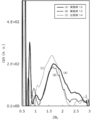
- the shortest inter-dot distance of semiconductor quantum dots can be obtained by structural evaluation of a quantum dot film having semiconductor quantum dots by a grazing incidence small angle X-ray scattering (GISAXS). . By such measurement, the center-to-center distance d between adjacent semiconductor quantum dots is obtained, and the shortest distance between dots is calculated by subtracting the particle diameter of the semiconductor quantum dots from the obtained center-to-center distance d.
- the average of the scattered X-rays for the semiconductor quantum dots existing in all the regions irradiated with the X-rays is detected as the measurement target scattered X-rays.
- the shortest dot-to-dot distance calculated based on the detected scattered X-rays is an “average shortest dot-to-dot distance” that is an average value of the shortest distances between dots.
- the photocurrent value of the semiconductor film can be improved as the average shortest distance between dots of the semiconductor quantum dots is smaller.
- the average shortest distance between dots is 0 nm, that is, the semiconductor quantum dots are in contact with each other, and the aggregated form is not different from the bulk semiconductor, and the characteristics of the semiconductor quantum dots that are nano-sized cannot be obtained.
- the average shortest distance between dots is preferably larger than 0 nm.
- the average shortest distance between dots of the semiconductor quantum dots is more preferably less than 0.30 nm, and further preferably less than 0.20 nm.
- the thickness of the semiconductor film is not particularly limited, but is preferably 10 nm or more and more preferably 50 nm or more from the viewpoint of obtaining high electrical conductivity. In addition, the thickness of the semiconductor film is preferably 300 nm or less from the viewpoint of excessive carrier concentration and ease of manufacture.
- the manufacturing method of the semiconductor film of the present invention is not particularly limited, it is manufactured by the semiconductor film manufacturing method of the present invention from the viewpoint of shortening the interval between the semiconductor quantum dots and arranging the semiconductor quantum dots densely. It is preferable to do.
- a semiconductor quantum dot dispersion liquid containing a semiconductor quantum dot, a first ligand coordinated to the semiconductor quantum dot, and a first solvent is applied onto the substrate.
- the molecular chain length is shorter than that of the first ligand and the arrangement represented by the general formula (A)
- a second ligand and a second solvent which are at least one selected from a ligand, a ligand represented by formula (B), and a ligand represented by formula (C)
- X 1 represents —SH, —NH 2 , or —OH
- a 1 and B 1 each independently represent a hydrogen atom or a substituent having 1 to 10 atoms.
- X 1 represents —SH or —OH
- X 2 represents —SH, —NH 2 , or —OH
- a 2 and B 2 each independently represent a hydrogen atom or a substituent having 1 to 10 atoms.
- a 3 represents a hydrogen atom or atoms of 1 to 10 substituents.
- the semiconductor quantum dot assembly forming step and the ligand exchange step may be repeated, and further, a dispersion drying step for drying the semiconductor quantum dot dispersion, a ligand solution A solution drying step for drying the substrate, a washing step for washing the semiconductor quantum dot aggregate on the substrate, and the like.
- a semiconductor quantum dot dispersion is applied to the substrate to form an assembly of semiconductor quantum dots on the substrate.
- the semiconductor quantum dots are dispersed in the first solvent by the first ligand having a molecular chain length longer than that of the second ligand, the semiconductor quantum dots are less likely to be in an aggregated bulk shape. . Therefore, by applying the semiconductor quantum dot dispersion liquid onto the substrate, the semiconductor quantum dot aggregate can be configured so that the semiconductor quantum dots are arranged one by one.
- the first ligand coordinated to the semiconductor quantum dot and the first coordination by applying a solution of the specific ligand to the aggregate of semiconductor quantum dots by the ligand exchange step Ligand exchange is performed with a second ligand (specific ligand) having a molecular chain length shorter than that of the child.
- the specific ligand has an amino group in the molecule as shown in the general formulas (A) to (C). As described above, the amino group has a high complex stability constant.
- the metal atom of the semiconductor quantum dot and —SH represented by X 1 (or X 2 ) are used. , -NH 2 or -OH.
- the amino group is considered to promote the complex formation between the metal atom of the semiconductor quantum dot and the OH of the carboxy group. Therefore, the second ligand (specific ligand) is coordinated by replacing the first ligand having a molecular chain length longer than that of the second ligand, and the coordination bond with the semiconductor quantum dot. Therefore, it is considered that the semiconductor quantum dots are easily brought close to each other. When the semiconductor quantum dots are brought close to each other, it is considered that the electrical conductivity of the aggregate of semiconductor quantum dots is increased and a semiconductor film having a high photocurrent value can be obtained. Furthermore, it is considered that the semiconductor quantum dots are connected to each other by a coordinate bond through a specific ligand, whereby the aggregate of semiconductor quantum dots becomes a strong semiconductor film and hardly peels off from the substrate.
- a semiconductor quantum dot dispersion liquid containing a semiconductor quantum dot, a first ligand coordinated to the semiconductor quantum dot, and a first solvent is applied on the substrate to form the semiconductor quantum dot To form an aggregate.
- the semiconductor quantum dot dispersion liquid may be applied to the substrate surface, or may be applied to another layer provided on the substrate. Examples of other layers provided on the substrate include an adhesive layer and a transparent conductive layer for improving the adhesion between the substrate and the assembly of semiconductor quantum dots.
- the semiconductor quantum dot dispersion liquid contains a semiconductor quantum dot having a metal atom, a first ligand, and a first solvent.
- the semiconductor quantum dot dispersion liquid may further contain other components as long as the effects of the present invention are not impaired.
- the details of the semiconductor quantum dots containing metal atoms contained in the semiconductor quantum dot dispersion liquid are as described above, and the preferred embodiments are also the same.
- the content of the semiconductor quantum dots in the semiconductor quantum dot dispersion liquid is preferably 1 mg / ml to 100 mg / ml, and more preferably 5 mg / ml to 40 mg / ml. When the content of the semiconductor quantum dots in the semiconductor quantum dot dispersion liquid is 1 mg / ml or more, the semiconductor quantum dot density on the substrate is increased, and a good film is easily obtained.
- the content of the semiconductor quantum dots is 100 mg / ml or less
- the film thickness of the film obtained when the semiconductor quantum dot dispersion liquid is applied once is hardly increased. Therefore, the ligand exchange of the 1st ligand coordinated to the semiconductor quantum dot in a film
- membrane can fully be performed.
- the first ligand contained in the semiconductor quantum dot dispersion liquid functions as a ligand coordinated to the semiconductor quantum dot and has a molecular structure that is likely to cause steric hindrance, and the semiconductor quantum in the first solvent. It also serves as a dispersant for dispersing dots.
- the first ligand has a longer molecular chain length than the second ligand described later. The length of the molecular chain is determined by the length of the main chain when there is a branched structure in the molecule.
- “dispersion” refers to a state where there is no sedimentation or turbidity of particles.
- the first ligand is preferably a ligand having at least 6 carbon atoms in the main chain, and a ligand having 10 or more carbon atoms in the main chain. Is more desirable.
- the first ligand may be either a saturated compound or an unsaturated compound. Decanoic acid, lauric acid, myristic acid, palmitic acid, stearic acid, behenic acid, oleic acid, erucic acid, oleylamine , Dodecylamine, dodecanethiol, 1,2-hexadecanethiol, trioctylphosphine oxide, cetrimonium bromide and the like.
- the first ligand is preferably one that hardly remains in the film when the semiconductor film is formed.
- the first ligand is preferably at least one of oleic acid and oleylamine, from the viewpoint of making the semiconductor quantum dots have dispersion stability and hardly remaining in the semiconductor film.
- the content of the first ligand in the semiconductor quantum dot dispersion is preferably 10 mmol / l to 200 mmol / l with respect to the total volume of the semiconductor quantum dot dispersion.
- the first solvent contained in the semiconductor quantum dot dispersion liquid is not particularly limited, but is preferably a solvent that hardly dissolves the semiconductor quantum dots and easily dissolves the first ligand.
- the first solvent is preferably an organic solvent, and specific examples include alkanes [n-hexane, n-octane, etc.], benzene, toluene and the like. Only 1 type may be sufficient as a 1st solvent and the mixed solvent which mixed 2 or more types may be sufficient as it.
- the first solvent is preferably a solvent that hardly remains in the formed semiconductor film. If the solvent has a relatively low boiling point, the content of residual organic substances can be suppressed when the semiconductor film is finally obtained. Furthermore, those with good wettability to the substrate are naturally preferable. For example, when coating on a glass substrate, alkanes such as hexane and octane are more preferable.
- the content of the first solvent in the semiconductor quantum dot dispersion is preferably 90% by mass to 98% by mass with respect to the total mass of the semiconductor quantum dot dispersion.
- the semiconductor quantum dot dispersion is applied on the substrate.
- the structure of the substrate may be a single layer structure or a laminated structure.
- a substrate made of glass, an inorganic material such as YSZ (Yttria-Stabilized Zirconia), a resin, a resin composite material, or the like can be used as the substrate.
- a substrate made of a resin or a resin composite material is preferable from the viewpoint of light weight and flexibility.
- Resins include polybutylene terephthalate, polyethylene terephthalate, polyethylene naphthalate, polybutylene naphthalate, polystyrene, polycarbonate, polysulfone, polyethersulfone, polyarylate, allyl diglycol carbonate, polyamide, polyimide, polyamideimide, polyetherimide, poly Fluorine resins such as benzazole, polyphenylene sulfide, polycycloolefin, norbornene resin, polychlorotrifluoroethylene, liquid crystal polymer, acrylic resin, epoxy resin, silicone resin, ionomer resin, cyanate resin, crosslinked fumaric acid diester, cyclic polyolefin, aromatic Synthetic resins such as aromatic ethers, maleimide-olefins, cellulose, episulfide compounds, etc. .
- a composite plastic material of a resin and the following inorganic material can be given. That is, composite plastic material of resin and silicon oxide particles, composite plastic material of resin and metal nanoparticles, composite plastic material of resin and inorganic oxide nanoparticles, composite plastic material of resin and inorganic nitride nanoparticles, Composite plastic material of resin and carbon fiber, composite plastic material of resin and carbon nanotube, composite plastic material of resin and glass flake, composite plastic material of resin and glass fiber, composite plastic material of resin and glass beads, Composite plastic material of resin and clay mineral, Composite plastic material of resin and particles having mica derivative crystal structure, Laminated plastic material having at least one bonding interface between resin and thin glass, Inorganic layer and organic layer By laminating alternately, at least one or more Composite material or the like having a barrier property with the bonding interface.
- an aluminum substrate or an aluminum substrate with an oxide film whose surface insulation is improved by subjecting the surface to oxidation treatment (for example, anodization treatment). Also good.
- a substrate made of resin or resin composite material is excellent in heat resistance, dimensional stability, solvent resistance, electrical insulation, workability, low air permeability, low moisture absorption, etc. It is preferable.
- the resin substrate and the resin composite material substrate may include a gas barrier layer for preventing permeation of moisture, oxygen, etc., an undercoat layer for improving the flatness of the resin substrate and the adhesion to the lower electrode, and the like. Good.
- a lower electrode, an insulating film, or the like may be provided on the substrate. In that case, a semiconductor quantum dot dispersion liquid is applied to the lower electrode or the insulating film on the substrate.
- the thickness of the substrate is not particularly limited, but is preferably 50 ⁇ m to 1000 ⁇ m, and more preferably 50 ⁇ m to 500 ⁇ m.
- the thickness of the substrate is 50 ⁇ m or more, the flatness of the substrate itself is improved, and when the thickness of the substrate is 1000 ⁇ m or less, the flexibility of the substrate itself is improved and the semiconductor film can be used as a flexible semiconductor device. It becomes easier.
- the method for applying the semiconductor quantum dot dispersion on the substrate is not particularly limited, and examples thereof include a method of applying the semiconductor quantum dot dispersion on the substrate, a method of immersing the substrate in the semiconductor quantum dot dispersion, and the like. More specifically, as a method of applying the semiconductor quantum dot dispersion liquid on the substrate, spin coating method, dipping method, ink jet method, dispenser method, screen printing method, letterpress printing method, intaglio printing method, spray coating method, etc. The liquid phase method can be used.
- the inkjet method, the dispenser method, the screen printing method, the relief printing method, and the intaglio printing method can form a coating film at an arbitrary position on the substrate and do not require a patterning step after the film formation. Therefore, the process cost can be reduced.
- the semiconductor quantum dot aggregate formed on the substrate by the semiconductor quantum dot aggregate formation step has a molecular chain length shorter than that of the first ligand, and a general formula (A ), A ligand represented by the general formula (B), and a second ligand that is at least one selected from a ligand represented by the general formula (C) And a solution containing the second solvent, the first ligand coordinated to the semiconductor quantum dots as the second ligand (specific ligand) contained in the ligand solution Exchange.
- the ligand solution contains at least a second ligand (specific ligand) and a second solvent.
- the ligand solution may further contain other components as long as the effects of the present invention are not impaired.
- the second ligand is the specific ligand described above, and the molecular chain length is shorter than that of the first ligand.
- the method for determining the length of the molecular chain length of the ligand is as described in the description of the first ligand.
- the details of the specific ligand are also as described above.
- a specific ligand has a hydroxyl group (OH) in a molecule
- OH hydroxyl group
- numerator When the specific ligand has a hydroxy group in the molecular structure, miscibility with alcohol can be increased.
- when performing ligand exchange of a semiconductor quantum dot by the ligand solution containing the specific ligand which has a hydroxyl group when alcohol is used as a 2nd solvent, ligand exchange is efficiently performed. It can be carried out.
- the content of the specific ligand in the ligand solution is preferably 5 mmol / l to 200 mmol / l, more preferably 10 mmol / l to 100 mmol / l with respect to the total volume of the ligand solution. .
- the second solvent contained in the ligand solution is not particularly limited, but is preferably a solvent that easily dissolves the specific ligand.
- a solvent is preferably an organic solvent having a high dielectric constant, and examples thereof include ethanol, acetone, methanol, acetonitrile, dimethylformamide, dimethyl sulfoxide, butanol, and propanol. Only 1 type may be sufficient as a 2nd solvent, and the mixed solvent which mixed 2 or more types may be sufficient as it.
- the second solvent is preferably a solvent that hardly remains in the formed semiconductor film. From the viewpoint of easy drying and easy removal by washing, an alcohol or alkane having a low boiling point is preferable, and methanol, ethanol, n-hexane, or n-octane is more preferable.
- the second solvent is preferably not mixed with the first solvent.
- the second solvent is methanol or acetone. It is preferable to use a polar solvent such as
- content of the 2nd solvent in a ligand solution is the remainder which deducted content of the specific ligand from the ligand solution total mass.
- the method of applying the ligand solution to the aggregate of semiconductor quantum dots is the same as the method of applying the semiconductor quantum dot dispersion on the substrate, and the preferred embodiment is also the same.
- the semiconductor quantum dot assembly forming step and the ligand exchange step may be repeated.
- the electrical conductivity of the semiconductor film having an assembly of semiconductor quantum dots coordinated with a specific ligand is increased, and the thickness of the semiconductor film is increased. Can be thickened.
- the semiconductor quantum dot assembly formation step and the ligand exchange step may be repeated separately, but the ligand exchange step is performed after the semiconductor quantum dot assembly formation step is performed. It is preferable to repeat the cycle.
- By repeating the set of the semiconductor quantum dot assembly forming step and the ligand exchange step unevenness of ligand exchange can be easily suppressed.
- the photocurrent value of the semiconductor film increases as the exchange rate of the semiconductor quantum dot aggregate to the specific ligand in the ligand exchange increases.
- the ligand exchange between the first ligand and the second ligand (specific ligand) of the semiconductor quantum dot is performed in at least a part of the semiconductor quantum dot assembly. , 100% (number) may not replace the specific ligand.
- the manufacturing method of the semiconductor film of this invention may have the washing
- the washing step excess ligands and ligands desorbed from the semiconductor quantum dots can be removed. Further, the remaining solvent and other impurities can be removed.
- the cleaning of the semiconductor quantum dot aggregate is performed by pouring at least one of the first solvent and the second solvent on the semiconductor quantum dot aggregate, or by removing the substrate on which the semiconductor quantum dot aggregate or the semiconductor film is formed. What is necessary is just to immerse in at least one of 1 solvent and 2nd solvent.
- the cleaning by the cleaning process may be performed after the semiconductor quantum dot assembly forming process or may be performed after the ligand exchange process. Moreover, you may carry out after the repetition of the set of a semiconductor quantum dot aggregate formation process and a ligand exchange process.
- the manufacturing method of the semiconductor film of this invention may have a drying process.
- the drying step may be a dispersion drying step for drying the solvent remaining in the semiconductor quantum dot assembly after the semiconductor quantum dot assembly forming step, or the ligand solution may be replaced with a ligand solution after the ligand exchange step. It may be a solution drying step for drying.
- the comprehensive process performed after the repetition of the set of a semiconductor quantum dot aggregate formation process and a ligand exchange process may be sufficient.
- a semiconductor film is manufactured on the substrate through the steps described above. Since the obtained semiconductor film is formed by connecting semiconductor quantum dots with a specific ligand shorter than the conventional one, the electrical conductivity is high and a high photocurrent value is obtained. In addition, since the specific ligand has a high complex stability constant, the semiconductor film of the present invention composed of the semiconductor quantum dots and the specific ligand has stable coordination bonds, excellent film strength, Peeling is also suppressed.
- the semiconductor film of the present invention has photoelectric conversion characteristics and hardly peels off, and thus can be suitably applied to various electronic devices having a semiconductor film or a photoelectric conversion film.
- the semiconductor film of the present invention includes a photoelectric conversion film of a solar cell, a light emitting diode (LED), a semiconductor layer (active layer) of a thin film transistor, a photoelectric conversion film of an indirect radiation imaging apparatus, and a visible to infrared region. It can be suitably applied to a photodetector or the like.
- a solar cell will be described as an example of an electronic device including the semiconductor film of the present invention or the semiconductor film manufactured by the method of manufacturing a semiconductor film of the present invention.
- a pn junction solar cell can be obtained by using a semiconductor film device having a pn junction including a p-type semiconductor layer including the semiconductor film of the present invention and an n-type semiconductor layer.
- a pn junction solar cell for example, a p-type semiconductor layer and an n-type semiconductor layer are provided adjacent to each other on a transparent conductive film formed on a transparent substrate.
- a form in which a metal electrode is formed on the n-type semiconductor layer is exemplified.
- FIG. 1 shows a schematic cross-sectional view of a pn junction solar cell 100 according to an embodiment of the present invention.
- a pn junction solar cell 100 includes a transparent substrate 10, a transparent conductive film 12 provided on the transparent substrate 10, a p-type semiconductor layer 14 formed of the semiconductor film of the present invention on the transparent conductive film 12, and p An n-type semiconductor layer 16 and a metal electrode 18 provided on the n-type semiconductor layer 16 are stacked on the type semiconductor layer 14.
- the p-type semiconductor layer 14 and the n-type semiconductor layer 16 are laminated adjacent to each other, a pn junction solar cell can be obtained.
- the transparent substrate 10 the same material as the substrate used in the method for producing a semiconductor film of the present invention can be used as long as it is transparent. Specifically, a glass substrate, a resin substrate, etc. are mentioned.
- the transparent conductive film 12 includes a film composed of In 2 O 3 : Sn (ITO), SnO 2 : Sb, SnO 2 : F, ZnO: Al, ZnO: F, CdSnO 4 and the like. .
- the n-type semiconductor layer 16 is preferably a metal oxide. Specific examples include metal oxides containing at least one of Ti, Zn, Sn, and In, and more specific examples include TiO 2 , ZnO, SnO 2 , and IGZO.
- the n-type semiconductor layer is preferably formed by a wet method (also referred to as a liquid phase method) in the same manner as the p-type semiconductor layer from the viewpoint of manufacturing cost.
- a wet method also referred to as a liquid phase method
- the metal electrode 18 Pt, Al, Cu, Ti, Ni, or the like can be used.
- PbS particle dispersion 1 a PbS particle dispersion in which PbS particles were dispersed in toluene was prepared.
- PbS core Evidot nominal particle size 3.3 nm, 20 mg / ml, solvent toluene
- 2 ml of the PbS particle dispersion was taken into the centrifuge tube, 38 ⁇ l of oleic acid was added, and then 20 ml of toluene was added to dilute the concentration of the dispersion.
- the obtained dispersion was concentrated using a rotary evaporator (35 hpa, 40 ° C.), and as a result, about 4 ml of semiconductor quantum dot dispersion 1 (octane solvent) having a concentration of about 10 mg / ml was obtained.
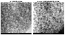
- the average particle diameter of the PbS particles contained in the semiconductor quantum dot dispersion liquid 1 was 3 nm.
- the average particle diameter of the semiconductor quantum dots was calculated as an average of 10 semiconductor quantum dots by photographic observation in TEM (Transmission Electron Microscope) measurement. A TEI 80-300 manufactured by FEI Co. was used as a measuring device.
- the product was taken out from the three-necked round bottom flask, and unreacted products and by-products were removed by centrifugation using a centrifuge.
- the product (InP particles) was purified using ultra-dehydrated toluene as a good solvent and dehydrated ethanol as a poor solvent. Specifically, the process of dissolving the product in a good solvent, redispersing the dissolved InP particles in a poor solvent, and centrifuging the resulting InP particle dispersion was repeated. An ultrasonic cleaner was used for redispersion. After repeated centrifugation of the InP particle dispersion, dehydrated ethanol remaining in the InP particle dispersion was removed by distillation under reduced pressure using a rotary evaporator.
- the extracted InP particles were dispersed in octane to obtain an octane dispersion having an oleylamine-modified InP particle concentration of 1 mg / ml. This was designated as semiconductor quantum dot dispersion 2.
- the three-necked flask is cooled to room temperature and aerated with nitrogen gas, and then a solution containing 2.57 mmol of hexamethyldisilazian and 5 ml of 1-octadecene is injected into the three-necked flask with a syringe.
- the septum cap was stabbed with a syringe needle and injected).
- the three-necked flask was heated to 120 ° C. over 40 minutes and held for 1 minute, and then the three-necked flask was cooled to room temperature with a cooling fan.
- a substrate having 65 pairs of comb-shaped platinum electrodes shown in FIG. 2 on a quartz glass was prepared.
- a comb-type platinum electrode (model number 012126, electrode interval 5 ⁇ m) manufactured by BAS was used.
- Table 1 shows the combinations of the semiconductor quantum dot dispersion liquid and the ligand solution in Examples and Comparative Examples.
- PbS in the “seed” column of the “semiconductor quantum dot” column means that the semiconductor quantum dot dispersion liquid 1 was used
- InP means that the semiconductor quantum dot dispersion liquid 2 was used.
- the types of ligands contained in the ligand solution are the ligands shown in the “Compound Name” column of the “Ligand” column of Table 1.
- A in the “ligand”, “general formula”, and “seed” columns means that the ligand is represented by the general formula (A), and “B” means that the ligand is represented by the general formula. It means that it is represented by (B), and “C” means that the ligand is represented by the general formula (C).
- Ligands that cannot be represented by the general formulas (A), (B), and (C) are represented by “ ⁇ ”. “Number of A” represents the number of atoms of A 1 , A 2 or A 3 , and “Number of B” represents the number of atoms of B 1 or B 2 .
- the ligand used in Comparative Example 4 is potassium bromide (KBr), and the ligand used in Comparative Example 5 is cetyltrimethylammonium bromide [(CH 3 (CH 2 ) 15 N ( CH 3 ) 3 ) + , Br ⁇ ].
- the electrical conductivity of the semiconductor film was evaluated by using a semiconductor parameter analyzer for the produced semiconductor film device. First, the voltage applied to the electrodes was swept between ⁇ 5 to 5 V without irradiating the semiconductor film device with light, and the IV characteristics in the dark state were obtained. The current value with a +5 V bias applied was adopted as the dark current value Id. Next, to evaluate the photocurrent values while irradiating monochromatic light (irradiation intensity 10 13 photons) to the semiconductor film device. The semiconductor film device was irradiated with monochrome light using the apparatus shown in FIG. The wavelength of the monochromatic light was systematically changed between 280 nm and 700 nm. The increase in current from the dark current when irradiating light with a wavelength of 280 nm was taken as the photocurrent value Ip. The evaluation results are shown in Table 1.
- the electrical conductivity of the semiconductor film is improved by bringing the semiconductor quantum dots close to each other using a specific ligand. can do.
- the semiconductor quantum dots are too close to each other, the semiconductor quantum dots are likely to be aggregated.
- Semiconductor quantum dots are expected to become bulky when aggregated.
- the semiconductor film desirably retains physical properties as a semiconductor quantum dot while exhibiting good electrical characteristics. In particular, when considering application of a semiconductor film to an LED or a solar cell, it is difficult to obtain absorption and emission of a target wavelength unless the semiconductor film has physical properties as a semiconductor quantum dot.
- the film of Comparative Example 11 was obtained in the same manner as in Example 1 except that the ligand solution obtained in the same manner as in Example 1 except that the ligand was changed to glycolic acid. It is.
- the film of Comparative Example 12 is a film obtained in Example 1 without performing the steps (2) and (3) among the steps (1) to (4) in “Manufacturing the semiconductor film”. .
- the film of Comparative Example 12 was an insulating film that did not exhibit electrical conductivity because the semiconductor quantum dots were not close to each other.
- the PbS bulk is a general II-VI group semiconductor, which is a single crystal of PbS, has a size larger than 100 nm, and has no quantum size effect.
- FIG. 6 An experimental setup used for photoluminescence measurement is schematically shown in FIG.
- This experimental apparatus mainly includes a laser irradiator 20, a total reflection mirror 22, a dichroic mirror 24, lenses 26 and 28, and a spectroscope 32.
- the laser light emitted from the laser irradiator 20 is converted into a total reflection mirror 22,
- the structure reaches the measurement sample (semiconductor film of the evaluation device) 30 and the spectroscope 32 through the dichroic mirror 24 and the lenses 26 and 28, respectively.
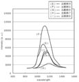
- 6 to 8 show PL spectra.
- FIG. 6 shows PL spectra of Example 1 (curve A), Example 2 (curve B), and Comparative Example 12 (curve C).
- FIG. 6 shows PL spectra of Example 1 (curve A), Example 2 (curve B), and Comparative Example 12 (curve C).
- FIG. 7 shows the PL spectra of Comparative Example 1 (curve D) and Comparative Example 12 (curve C), and FIG. 8 shows the PL spectra of Comparative Examples 4 to 8 (curve E to curve I).
- the peak wavelengths in each ligand are summarized in Table 2.
- the peak wavelength of the PbS semiconductor quantum dots (Comparative Example 12) in which oleic acid was coordinated without ligand exchange was about 1100 nm.
- the semiconductor film excluding the semiconductor film coordinated with 2-aminoethane-1-thiol (Example 1), it can be seen that the peak wavelength is shifted to the long wave side by about 60 nm to 120 nm.
- the shift of the peak wavelength to the long wavelength side is because the confinement potential of the semiconductor quantum dots is reduced due to the proximity of the semiconductor quantum dots by ligand exchange, and the band gap is effectively reduced. is there.
- the decrease in the band gap is the largest and is about 100 meV.
- Example 1 and Example 2 the semiconductor film of semiconductor quantum dots coordinated with a specific ligand has a short semiconductor quantum dot interval and high electrical conduction through the semiconductor quantum dots. While exhibiting the characteristics, it was confirmed that the physical properties (band gap, etc.) of the semiconductor quantum dots were retained.
- the peak wavelength appears in the vicinity of 1290 nm for the semiconductor film of the semiconductor quantum dots coordinated with 2-aminoethanethiol (Example 1).
- the emission peak of the semiconductor film of Example 1 is different from the emission peak of the bulk and the emission peak of the normal semiconductor quantum dot, and the energy level of the semiconductor quantum dot is modulated when the semiconductor quantum dots are very close to each other. This result suggests the formation of a new energy level.
- Average particle diameter of semiconductor quantum dots The average particle diameter of the semiconductor quantum dots was measured with a TEM apparatus. As a measuring apparatus, TITAN 80-300 manufactured by FEI was used. Two types of samples were prepared. One is a sample obtained by drop-casting the semiconductor quantum dot dispersion 1 on a Si substrate, collected by a sampling knife, and placed on a measurement stage. The other is that a spin coat film having undergone ligand exchange with ethanedithiol is formed on a quartz glass substrate, and is similarly collected with a sampling knife. In other words, the latter sample is a semiconductor film obtained in the same manner except that a quartz glass substrate was used as the substrate in the production of the semiconductor film of Comparative Example 1.
- FIG. 9 shows a TEM image when the semiconductor quantum dot dispersion liquid 1 is drop-cast. From FIG. 9, it was confirmed that the average particle diameter (average of 10 dots) of the quantum dots was 3 nm. In addition, since the oleic acid, which is a long chain fatty acid, remains coordinated without ligand exchange, it can be seen that the interval between the semiconductor quantum dots is very wide (2 nm to 4 nm).
- FIG. 1 a TEM image of the spin coat film after ligand exchange is shown in FIG.
- the semiconductor film of the present invention in which the specific ligand is coordinated to the semiconductor quantum dots is the proximity of the semiconductor quantum dots.
- Example 12 The structure of the obtained quantum dot films (samples) of Example 12, Example 13, Comparative Example 14, and Comparative Example 15 was evaluated by a small angle incident X-ray small angle scattering method (GISAXS).
- the incident light is Cu K ⁇ rays
- the quantum dot film is irradiated with X-rays at an incident angle (about 0.4 °) slightly larger than the total reflection angle, and the detector is scanned in the in-plane direction. Scattered light was detected.
- FIG. 11 shows the in-plane angle dependence of the scattered light obtained by subtracting the background structure of the scattered light with respect to each ligand type for the semiconductor films of Example 12, Example 13, and Comparative Example 14.
- ⁇ is the wavelength of incident light.
- Table 3 shows the shortest distance between adjacent quantum dots calculated from the scattering peak (the measured distance between centers of quantum dots d minus the particle diameter of the quantum dots).
- the detected scattered light is an average of scattered X-rays for samples present in all regions irradiated with X-rays in the measurement apparatus.
- the average shortest distance between dots is smaller than the conventional semiconductor film coordinated with ethanedithiol (less than 0.45 nm) It was found that a high photocurrent value and a high dark current value can be obtained.
- the semiconductor film coordinated with ethanedithiol remarkable film peeling occurred with the naked eye, whereas for the semiconductor film coordinated with the specific ligand of the example, no film peeling was observed and good Roughness was realized.
- the average shortest distance between dots is preferably less than 0.3 nm, more preferably 2-aminoethane. As in the case of -1-thiol coordination, it has been found that the average shortest distance between dots is preferably less than 0.2 nm.
Landscapes
- Engineering & Computer Science (AREA)
- Chemical & Material Sciences (AREA)
- Physics & Mathematics (AREA)
- Condensed Matter Physics & Semiconductors (AREA)
- General Physics & Mathematics (AREA)
- Manufacturing & Machinery (AREA)
- Power Engineering (AREA)
- Microelectronics & Electronic Packaging (AREA)
- Computer Hardware Design (AREA)
- Nanotechnology (AREA)
- Crystallography & Structural Chemistry (AREA)
- Organic Chemistry (AREA)
- Materials Engineering (AREA)
- Composite Materials (AREA)
- Theoretical Computer Science (AREA)
- Mathematical Physics (AREA)
- Health & Medical Sciences (AREA)
- Life Sciences & Earth Sciences (AREA)
- Biochemistry (AREA)
- General Health & Medical Sciences (AREA)
- Molecular Biology (AREA)
- Photovoltaic Devices (AREA)
- Electroluminescent Light Sources (AREA)
- Thin Film Transistor (AREA)
Priority Applications (1)
| Application Number | Priority Date | Filing Date | Title |
|---|---|---|---|
| US14/699,817 US10050161B2 (en) | 2012-10-31 | 2015-04-29 | Semiconductor film, method of producing semiconductor film, solar cell, light-emitting diode, thin film transistor, and electronic device |
Applications Claiming Priority (4)
| Application Number | Priority Date | Filing Date | Title |
|---|---|---|---|
| JP2012241230 | 2012-10-31 | ||
| JP2012-241230 | 2012-10-31 | ||
| JP2012-282431 | 2012-12-26 | ||
| JP2012282431A JP6086721B2 (ja) | 2012-10-31 | 2012-12-26 | 半導体膜、半導体膜の製造方法、太陽電池、発光ダイオード、薄膜トランジスタ、および、電子デバイス |
Related Child Applications (1)
| Application Number | Title | Priority Date | Filing Date |
|---|---|---|---|
| US14/699,817 Continuation US10050161B2 (en) | 2012-10-31 | 2015-04-29 | Semiconductor film, method of producing semiconductor film, solar cell, light-emitting diode, thin film transistor, and electronic device |
Publications (1)
| Publication Number | Publication Date |
|---|---|
| WO2014069211A1 true WO2014069211A1 (ja) | 2014-05-08 |
Family
ID=50627125
Family Applications (1)
| Application Number | Title | Priority Date | Filing Date |
|---|---|---|---|
| PCT/JP2013/077668 Ceased WO2014069211A1 (ja) | 2012-10-31 | 2013-10-10 | 半導体膜および半導体膜の製造方法 |
Country Status (3)
| Country | Link |
|---|---|
| US (1) | US10050161B2 (enExample) |
| JP (1) | JP6086721B2 (enExample) |
| WO (1) | WO2014069211A1 (enExample) |
Families Citing this family (5)
| Publication number | Priority date | Publication date | Assignee | Title |
|---|---|---|---|---|
| JP5964744B2 (ja) * | 2012-12-26 | 2016-08-03 | 富士フイルム株式会社 | 半導体膜の製造方法 |
| CN116847702A (zh) | 2016-07-20 | 2023-10-03 | 索尼公司 | 半导体膜的制造方法 |
| EP3399344B1 (en) * | 2017-05-03 | 2021-06-30 | ams International AG | Semiconductor device for indirect detection of electromagnetic radiation and method of production |
| KR102584733B1 (ko) * | 2018-09-30 | 2023-10-05 | 티씨엘 테크놀로지 그룹 코포레이션 | 퀀텀닷 |
| JP7589454B2 (ja) * | 2020-06-17 | 2024-11-26 | artience株式会社 | 光電変換素子及び光電変換層形成用組成物 |
Citations (5)
| Publication number | Priority date | Publication date | Assignee | Title |
|---|---|---|---|---|
| JP2002048795A (ja) * | 2000-07-31 | 2002-02-15 | Mitsubishi Chemicals Corp | オリゴペプチド残基を結合してなる半導体超微粒子 |
| JP2003286292A (ja) * | 2002-01-28 | 2003-10-10 | Mitsubishi Chemicals Corp | 半導体超微粒子及びそれを含有してなる薄膜状成形体 |
| JP2004315661A (ja) * | 2003-04-16 | 2004-11-11 | Mitsubishi Chemicals Corp | 半導体超微粒子及び電界発光素子 |
| JP2009224714A (ja) * | 2008-03-18 | 2009-10-01 | Univ Of Tokyo | 有機薄膜トランジスタの製造方法 |
| WO2011005023A2 (en) * | 2009-07-08 | 2011-01-13 | Samsung Electronics Co., Ltd. | Semiconductor nanocrystal and preparation method thereof |
Family Cites Families (3)
| Publication number | Priority date | Publication date | Assignee | Title |
|---|---|---|---|---|
| WO2000017655A1 (en) | 1998-09-18 | 2000-03-30 | Massachusetts Institute Of Technology | Water-soluble fluorescent semiconductor nanocrystals |
| US20040007169A1 (en) | 2002-01-28 | 2004-01-15 | Mitsubishi Chemical Corporation | Semiconductor nanoparticles and thin film containing the same |
| KR20130067137A (ko) * | 2011-12-13 | 2013-06-21 | 삼성전자주식회사 | 양자점-매트릭스 박막 및 그의 제조방법 |
-
2012
- 2012-12-26 JP JP2012282431A patent/JP6086721B2/ja active Active
-
2013
- 2013-10-10 WO PCT/JP2013/077668 patent/WO2014069211A1/ja not_active Ceased
-
2015
- 2015-04-29 US US14/699,817 patent/US10050161B2/en active Active
Patent Citations (5)
| Publication number | Priority date | Publication date | Assignee | Title |
|---|---|---|---|---|
| JP2002048795A (ja) * | 2000-07-31 | 2002-02-15 | Mitsubishi Chemicals Corp | オリゴペプチド残基を結合してなる半導体超微粒子 |
| JP2003286292A (ja) * | 2002-01-28 | 2003-10-10 | Mitsubishi Chemicals Corp | 半導体超微粒子及びそれを含有してなる薄膜状成形体 |
| JP2004315661A (ja) * | 2003-04-16 | 2004-11-11 | Mitsubishi Chemicals Corp | 半導体超微粒子及び電界発光素子 |
| JP2009224714A (ja) * | 2008-03-18 | 2009-10-01 | Univ Of Tokyo | 有機薄膜トランジスタの製造方法 |
| WO2011005023A2 (en) * | 2009-07-08 | 2011-01-13 | Samsung Electronics Co., Ltd. | Semiconductor nanocrystal and preparation method thereof |
Also Published As
| Publication number | Publication date |
|---|---|
| JP6086721B2 (ja) | 2017-03-01 |
| JP2014112623A (ja) | 2014-06-19 |
| US10050161B2 (en) | 2018-08-14 |
| US20150236178A1 (en) | 2015-08-20 |
Similar Documents
| Publication | Publication Date | Title |
|---|---|---|
| JP6177515B2 (ja) | 半導体膜、半導体膜の製造方法、太陽電池、発光ダイオード、薄膜トランジスタ、および、電子デバイス | |
| JP5964744B2 (ja) | 半導体膜の製造方法 | |
| JP5955305B2 (ja) | 半導体膜、半導体膜の製造方法、太陽電池、発光ダイオード、薄膜トランジスタ、および、電子デバイス | |
| JP5995661B2 (ja) | 半導体膜、半導体膜の製造方法、太陽電池、発光ダイオード、薄膜トランジスタおよび電子デバイス | |
| JP5964742B2 (ja) | 半導体膜、半導体膜の製造方法、太陽電池、発光ダイオード、薄膜トランジスタ、および、電子デバイス | |
| Sliz et al. | Stable colloidal quantum dot inks enable inkjet-printed high-sensitivity infrared photodetectors | |
| Yamaguchi et al. | (Cd, Zn) S thin films prepared by chemical bath deposition for photovoltaic devices | |
| JP6086721B2 (ja) | 半導体膜、半導体膜の製造方法、太陽電池、発光ダイオード、薄膜トランジスタ、および、電子デバイス | |
| Geng et al. | Carbon quantum dots interfacial modified graphene/silicon Schottky barrier solar cell | |
| Atiq et al. | Interlayer effect on photoluminescence enhancement and band gap modulation in Ga-doped ZnO thin films | |
| Nawaz et al. | Flexible photodetectors with high responsivity and broad spectral response employing ternary Sn x Cd1–x S micronanostructures | |
| Mishra et al. | Structural, photoconductivity and photoluminescence characterization of cadmium sulfide quantum dots prepared by a co-precipitation method | |
| JP6008736B2 (ja) | 半導体膜、半導体膜の製造方法、太陽電池、発光ダイオード、薄膜トランジスタおよび電子デバイス | |
| Thomas et al. | An inverted ZnO/P3HT: PbS bulk-heterojunction hybrid solar cell with a CdSe quantum dot interface buffer layer | |
| Elkamel et al. | Effects of plasmon resonance on the low frequency noise and optoelectronic properties of Au/Cu codoped ZnO based photodetectors | |
| Tuc Altaf et al. | Self-Powered Photoelectrochemical Photodetectors Based on a CsPbBr3/S-g-C3N4 Heterojunction-Sensitized 3D ZnO Nanostructured Thin Film | |
| Winata et al. | Effect of UV-O3 treatment on the performance of UV detector based on zinc oxide/molybdenum disulfide nanosheet heterostructures | |
| Jiang et al. | Ultrafast-Speed, High-Response, and Broadband WSe2-Based Photodetector Achieved by Integrating Activated ZnO QDs | |
| JP6275441B2 (ja) | 半導体膜、酸化物微粒子分散液、半導体膜の製造方法、及び、薄膜トランジスタ | |
| Kong et al. | AgIn5S8/ZnS Quantum Dots for Luminescent Down-Shifting and Antireflective Layer in Enhancing Photovoltaic Performance | |
| Saleh et al. | Preparation and characterization of CuI/PVA–PEDOT: PSS core–shell for photovoltaic application | |
| Chen et al. | Dilute manganese-doped ZnO nanowires for high photoelectrical performance | |
| Wang et al. | Large Orthorhombic Polyhedral CsPbBr3 Nanocrystals for Ultrasensitive Photodetectors with Type‐I Structures | |
| Mustakim et al. | Preliminary study of effective copper indium sulfide (CuInS2) quantum dots as photo-sensitizer in solar cell | |
| Fahim et al. | Photodetector for visible light based on Fe (phen) 2 (SCN) 2 molecule |
Legal Events
| Date | Code | Title | Description |
|---|---|---|---|
| 121 | Ep: the epo has been informed by wipo that ep was designated in this application |
Ref document number: 13850547 Country of ref document: EP Kind code of ref document: A1 |
|
| NENP | Non-entry into the national phase |
Ref country code: DE |
|
| 122 | Ep: pct application non-entry in european phase |
Ref document number: 13850547 Country of ref document: EP Kind code of ref document: A1 |