WO2014067176A1 - 液晶组合物与液晶面板 - Google Patents
液晶组合物与液晶面板 Download PDFInfo
- Publication number
- WO2014067176A1 WO2014067176A1 PCT/CN2012/084558 CN2012084558W WO2014067176A1 WO 2014067176 A1 WO2014067176 A1 WO 2014067176A1 CN 2012084558 W CN2012084558 W CN 2012084558W WO 2014067176 A1 WO2014067176 A1 WO 2014067176A1
- Authority
- WO
- WIPO (PCT)
- Prior art keywords
- liquid crystal
- crystal composition
- substrate
- crystal panel
- alignment film
- Prior art date
- Legal status (The legal status is an assumption and is not a legal conclusion. Google has not performed a legal analysis and makes no representation as to the accuracy of the status listed.)
- Ceased
Links
- YDIFEPUTGBBLFH-UHFFFAOYSA-N C=C(C(F)(F)F)C(Oc(cc1)ccc1-c(cc1)ccc1OC(C(C(F)(F)F)=C)=O)=O Chemical compound C=C(C(F)(F)F)C(Oc(cc1)ccc1-c(cc1)ccc1OC(C(C(F)(F)F)=C)=O)=O YDIFEPUTGBBLFH-UHFFFAOYSA-N 0.000 description 1
- 0 CC(C(C(C(F)(F)F)=C)=O)=C(*)C(C(C(F)(F)F)=C)=O Chemical compound CC(C(C(C(F)(F)F)=C)=O)=C(*)C(C(C(F)(F)F)=C)=O 0.000 description 1
Classifications
-
- G—PHYSICS
- G02—OPTICS
- G02F—OPTICAL DEVICES OR ARRANGEMENTS FOR THE CONTROL OF LIGHT BY MODIFICATION OF THE OPTICAL PROPERTIES OF THE MEDIA OF THE ELEMENTS INVOLVED THEREIN; NON-LINEAR OPTICS; FREQUENCY-CHANGING OF LIGHT; OPTICAL LOGIC ELEMENTS; OPTICAL ANALOGUE/DIGITAL CONVERTERS
- G02F1/00—Devices or arrangements for the control of the intensity, colour, phase, polarisation or direction of light arriving from an independent light source, e.g. switching, gating or modulating; Non-linear optics
- G02F1/01—Devices or arrangements for the control of the intensity, colour, phase, polarisation or direction of light arriving from an independent light source, e.g. switching, gating or modulating; Non-linear optics for the control of the intensity, phase, polarisation or colour
- G02F1/13—Devices or arrangements for the control of the intensity, colour, phase, polarisation or direction of light arriving from an independent light source, e.g. switching, gating or modulating; Non-linear optics for the control of the intensity, phase, polarisation or colour based on liquid crystals, e.g. single liquid crystal display cells
- G02F1/133—Constructional arrangements; Operation of liquid crystal cells; Circuit arrangements
- G02F1/1333—Constructional arrangements; Manufacturing methods
- G02F1/1337—Surface-induced orientation of the liquid crystal molecules, e.g. by alignment layers
- G02F1/133711—Surface-induced orientation of the liquid crystal molecules, e.g. by alignment layers by organic films, e.g. polymeric films
-
- G—PHYSICS
- G02—OPTICS
- G02F—OPTICAL DEVICES OR ARRANGEMENTS FOR THE CONTROL OF LIGHT BY MODIFICATION OF THE OPTICAL PROPERTIES OF THE MEDIA OF THE ELEMENTS INVOLVED THEREIN; NON-LINEAR OPTICS; FREQUENCY-CHANGING OF LIGHT; OPTICAL LOGIC ELEMENTS; OPTICAL ANALOGUE/DIGITAL CONVERTERS
- G02F1/00—Devices or arrangements for the control of the intensity, colour, phase, polarisation or direction of light arriving from an independent light source, e.g. switching, gating or modulating; Non-linear optics
- G02F1/01—Devices or arrangements for the control of the intensity, colour, phase, polarisation or direction of light arriving from an independent light source, e.g. switching, gating or modulating; Non-linear optics for the control of the intensity, phase, polarisation or colour
- G02F1/13—Devices or arrangements for the control of the intensity, colour, phase, polarisation or direction of light arriving from an independent light source, e.g. switching, gating or modulating; Non-linear optics for the control of the intensity, phase, polarisation or colour based on liquid crystals, e.g. single liquid crystal display cells
- G02F1/133—Constructional arrangements; Operation of liquid crystal cells; Circuit arrangements
- G02F1/1333—Constructional arrangements; Manufacturing methods
- G02F1/1337—Surface-induced orientation of the liquid crystal molecules, e.g. by alignment layers
- G02F1/13378—Surface-induced orientation of the liquid crystal molecules, e.g. by alignment layers by treatment of the surface, e.g. embossing, rubbing or light irradiation
- G02F1/133788—Surface-induced orientation of the liquid crystal molecules, e.g. by alignment layers by treatment of the surface, e.g. embossing, rubbing or light irradiation by light irradiation, e.g. linearly polarised light photo-polymerisation
-
- C—CHEMISTRY; METALLURGY
- C09—DYES; PAINTS; POLISHES; NATURAL RESINS; ADHESIVES; COMPOSITIONS NOT OTHERWISE PROVIDED FOR; APPLICATIONS OF MATERIALS NOT OTHERWISE PROVIDED FOR
- C09K—MATERIALS FOR MISCELLANEOUS APPLICATIONS, NOT PROVIDED FOR ELSEWHERE
- C09K19/00—Liquid crystal materials
- C09K19/04—Liquid crystal materials characterised by the chemical structure of the liquid crystal components, e.g. by a specific unit
- C09K2019/0444—Liquid crystal materials characterised by the chemical structure of the liquid crystal components, e.g. by a specific unit characterized by a linking chain between rings or ring systems, a bridging chain between extensive mesogenic moieties or an end chain group
- C09K2019/0448—Liquid crystal materials characterised by the chemical structure of the liquid crystal components, e.g. by a specific unit characterized by a linking chain between rings or ring systems, a bridging chain between extensive mesogenic moieties or an end chain group the end chain group being a polymerizable end group, e.g. -Sp-P or acrylate
-
- C—CHEMISTRY; METALLURGY
- C09—DYES; PAINTS; POLISHES; NATURAL RESINS; ADHESIVES; COMPOSITIONS NOT OTHERWISE PROVIDED FOR; APPLICATIONS OF MATERIALS NOT OTHERWISE PROVIDED FOR
- C09K—MATERIALS FOR MISCELLANEOUS APPLICATIONS, NOT PROVIDED FOR ELSEWHERE
- C09K19/00—Liquid crystal materials
- C09K19/04—Liquid crystal materials characterised by the chemical structure of the liquid crystal components, e.g. by a specific unit
- C09K19/06—Non-steroidal liquid crystal compounds
- C09K19/08—Non-steroidal liquid crystal compounds containing at least two non-condensed rings
- C09K19/10—Non-steroidal liquid crystal compounds containing at least two non-condensed rings containing at least two benzene rings
- C09K19/12—Non-steroidal liquid crystal compounds containing at least two non-condensed rings containing at least two benzene rings at least two benzene rings directly linked, e.g. biphenyls
- C09K2019/121—Compounds containing phenylene-1,4-diyl (-Ph-)
- C09K2019/122—Ph-Ph
-
- C—CHEMISTRY; METALLURGY
- C09—DYES; PAINTS; POLISHES; NATURAL RESINS; ADHESIVES; COMPOSITIONS NOT OTHERWISE PROVIDED FOR; APPLICATIONS OF MATERIALS NOT OTHERWISE PROVIDED FOR
- C09K—MATERIALS FOR MISCELLANEOUS APPLICATIONS, NOT PROVIDED FOR ELSEWHERE
- C09K19/00—Liquid crystal materials
- C09K19/04—Liquid crystal materials characterised by the chemical structure of the liquid crystal components, e.g. by a specific unit
- C09K19/06—Non-steroidal liquid crystal compounds
- C09K19/08—Non-steroidal liquid crystal compounds containing at least two non-condensed rings
- C09K19/30—Non-steroidal liquid crystal compounds containing at least two non-condensed rings containing saturated or unsaturated non-aromatic rings, e.g. cyclohexane rings
- C09K19/3001—Cyclohexane rings
- C09K19/3003—Compounds containing at least two rings in which the different rings are directly linked (covalent bond)
- C09K2019/3004—Cy-Cy
-
- C—CHEMISTRY; METALLURGY
- C09—DYES; PAINTS; POLISHES; NATURAL RESINS; ADHESIVES; COMPOSITIONS NOT OTHERWISE PROVIDED FOR; APPLICATIONS OF MATERIALS NOT OTHERWISE PROVIDED FOR
- C09K—MATERIALS FOR MISCELLANEOUS APPLICATIONS, NOT PROVIDED FOR ELSEWHERE
- C09K19/00—Liquid crystal materials
- C09K19/52—Liquid crystal materials characterised by components which are not liquid crystals, e.g. additives with special physical aspect: solvents, solid particles
- C09K19/54—Additives having no specific mesophase characterised by their chemical composition
- C09K19/542—Macromolecular compounds
- C09K2019/548—Macromolecular compounds stabilizing the alignment; Polymer stabilized alignment
-
- G—PHYSICS
- G02—OPTICS
- G02F—OPTICAL DEVICES OR ARRANGEMENTS FOR THE CONTROL OF LIGHT BY MODIFICATION OF THE OPTICAL PROPERTIES OF THE MEDIA OF THE ELEMENTS INVOLVED THEREIN; NON-LINEAR OPTICS; FREQUENCY-CHANGING OF LIGHT; OPTICAL LOGIC ELEMENTS; OPTICAL ANALOGUE/DIGITAL CONVERTERS
- G02F1/00—Devices or arrangements for the control of the intensity, colour, phase, polarisation or direction of light arriving from an independent light source, e.g. switching, gating or modulating; Non-linear optics
- G02F1/01—Devices or arrangements for the control of the intensity, colour, phase, polarisation or direction of light arriving from an independent light source, e.g. switching, gating or modulating; Non-linear optics for the control of the intensity, phase, polarisation or colour
- G02F1/13—Devices or arrangements for the control of the intensity, colour, phase, polarisation or direction of light arriving from an independent light source, e.g. switching, gating or modulating; Non-linear optics for the control of the intensity, phase, polarisation or colour based on liquid crystals, e.g. single liquid crystal display cells
- G02F1/133—Constructional arrangements; Operation of liquid crystal cells; Circuit arrangements
- G02F1/1333—Constructional arrangements; Manufacturing methods
- G02F1/133397—Constructional arrangements; Manufacturing methods for suppressing after-image or image-sticking
-
- G—PHYSICS
- G02—OPTICS
- G02F—OPTICAL DEVICES OR ARRANGEMENTS FOR THE CONTROL OF LIGHT BY MODIFICATION OF THE OPTICAL PROPERTIES OF THE MEDIA OF THE ELEMENTS INVOLVED THEREIN; NON-LINEAR OPTICS; FREQUENCY-CHANGING OF LIGHT; OPTICAL LOGIC ELEMENTS; OPTICAL ANALOGUE/DIGITAL CONVERTERS
- G02F1/00—Devices or arrangements for the control of the intensity, colour, phase, polarisation or direction of light arriving from an independent light source, e.g. switching, gating or modulating; Non-linear optics
- G02F1/01—Devices or arrangements for the control of the intensity, colour, phase, polarisation or direction of light arriving from an independent light source, e.g. switching, gating or modulating; Non-linear optics for the control of the intensity, phase, polarisation or colour
- G02F1/13—Devices or arrangements for the control of the intensity, colour, phase, polarisation or direction of light arriving from an independent light source, e.g. switching, gating or modulating; Non-linear optics for the control of the intensity, phase, polarisation or colour based on liquid crystals, e.g. single liquid crystal display cells
- G02F1/133—Constructional arrangements; Operation of liquid crystal cells; Circuit arrangements
- G02F1/1333—Constructional arrangements; Manufacturing methods
- G02F1/1337—Surface-induced orientation of the liquid crystal molecules, e.g. by alignment layers
- G02F1/133742—Surface-induced orientation of the liquid crystal molecules, e.g. by alignment layers for homeotropic alignment
Definitions
- the present invention relates to a liquid crystal composition, and more particularly to a liquid crystal composition to which a trifluoromethyl polymerizable monomer is added and a vertical alignment type liquid crystal panel.
- Liquid crystal display is a flat panel display device that uses the characteristics of liquid crystal materials to display images. Compared with other display devices, it has the advantages of lightness, low driving voltage and low power consumption. Mainstream products in the consumer market.
- the main technical parameters for evaluating liquid crystal displays are: 1 contrast, 2 brightness, 3 response time and 4 viewing angles.
- the response time of a liquid crystal display is improved mainly by a liquid crystal panel containing a fast response liquid crystal composition.
- Fig. 1 is a schematic view showing the alignment process of a liquid crystal panel currently made of a fast response liquid crystal composition.
- the fast response liquid crystal composition 30' comprises a conventional one or more liquid crystal molecules 3' and a reactive monomer (RM) 32'.
- the liquid crystal composition 30' is diffused on the surface of the alignment film 20' of the substrate 10' by a dropping type implantation technique (ODF), and then subjected to a process such as application of a voltage, first ultraviolet irradiation, and second ultraviolet irradiation to complete the alignment process.
- ODF dropping type implantation technique
- a first object of the present invention is to provide a liquid crystal composition to which a polymerizable monomer is added, which is more likely to generate radicals under ultraviolet irradiation, thereby solving the problem of an increase in the curing ability of the RM monomer. Residual RM monomer, which improves image retention.
- a liquid crystal composition for fabricating a liquid crystal panel comprising: At least one polymerizable monomer; at least one liquid crystal molecule; and at least one diluent; the diluent is a liquid crystal compound containing one or more alkenyl groups;
- the polymerizable monomer is contained in a liquid crystal composition, and the polymerizable monomer has the following molecular formula
- the A group is a hard core and is represented by the following formula II: Formula II, wherein the X is selected from one of H, F or CH 3 .
- the liquid crystal molecules are vertically aligned liquid crystal molecules (VA-LC).
- the diluent is represented by the following formula III or IV:
- the liquid crystal composition is a liquid crystal composition of a dropping type injection technique.
- a liquid crystal composition for producing a liquid crystal panel comprising: at least one polymerizable monomer, at least one liquid crystal molecule, and at least one diluent ; among them,
- the A group is a hard core, and is represented by the following formula II; Formula II, wherein X is selected from one of H, F or CH 3 ;
- the liquid crystal molecules are conventional vertically aligned liquid crystal molecules
- 1 ⁇ represents a fluorenyl group having 1 to 10 carbon atoms, and 11 is 1 to 10.
- the present invention also provides a liquid crystal panel comprising a first substrate and a second substrate respectively disposed with an alignment film, and the liquid crystal composition is diffused and distributed on the surface of the alignment film of the first substrate and the second substrate .
- the alignment film is a vertical alignment type alignment film.
- the first substrate is a color filter substrate
- the second substrate is a thin film transistor array substrate.
- the liquid crystal composition is a liquid crystal composition of a dropping type injection technique.
- a liquid crystal panel including a first substrate and a second substrate respectively disposed with an alignment film, and diffusion distribution on the surface of the alignment film of the first substrate and the second substrate
- a liquid crystal composition comprising at least one liquid crystal molecule, at least one diluent, and at least one of the above polymerizable monomers;
- the liquid crystal molecules are conventional vertically aligned liquid crystal molecules;
- the polymerizable monomer is represented by the following formula I;
- the A group is a hard core, and is represented by the following formula II;
- Formula II, the X is selected from one of H, F or CH 3 ;
- the diluent is represented by the following formula III or IV;
- the A group is a hard core and contains at least one benzene ring; the 1 ⁇ represents a fluorenyl group having 1 to 10 carbon atoms, and n is 1 to 10; and the alignment film is a vertical alignment type alignment film.
- the liquid crystal molecules described in the present invention are vertically aligned liquid crystal molecules known in the art; and the alignment film is a vertical alignment type alignment film known in the art.
- the fluorenyl group having 1 to 10 carbon atoms means a linear or linear fluorenyl group having 1 to 10 carbon atoms. For example: methyl, ethyl, propyl, isopropyl, butyl, isobutyl, tert-butyl, sec-butyl, pentyl, neopentyl, and the like.
- the positive effect of the present invention is:
- the polymerizable monomer provided by the present invention belongs to a reactive monomer (RM), which is more likely to generate free radicals under ultraviolet irradiation, thereby solving the RM single problem caused by the improvement of the curing ability of the RM monomer. Residue, which improves image retention.
- RM reactive monomer
- Figure 1 is a schematic view showing the alignment process of a liquid crystal panel currently made of a fast response liquid crystal composition
- Fig. 2 is a liquid crystal panel including the liquid crystal composition of the present invention.
- Figure 3 is a schematic view showing the alignment process of a liquid crystal panel made of the liquid crystal composition of the present invention.
- This embodiment provides a polymerizable monomer, which is contained in a liquid crystal composition, wherein the polymerizable monomer is
- a group is a hard core, and is represented by the following formula II; Formulas II, X is selected from one of the 3 H, F or CH.
- This embodiment provides a polymerizable monomer which is contained in a liquid crystal composition, and the polymerizable monomer is represented by the following formula V: Formula V, wherein X is selected from H, F or CH 3
- the preparation route of the polymerizable monomer of the formula V is as follows:
- the specific preparation method is as follows:
- Embodiment 3 provides a liquid crystal composition for fabricating a liquid crystal panel, the liquid crystal composition comprising: At least one polymerizable monomer represented by Formula V, at least one liquid crystal molecule, and at least one diluent.
- the liquid crystal molecules are liquid crystal molecules which are vertically aligned as known in the art.
- the diluent is a liquid crystal compound containing one or more alkenyl groups, and the following formula III IV represents:
- 1 ⁇ represents a fluorenyl group having 1 to 10 carbon atoms, and 11 is 1 to 10.
- This embodiment provides a liquid crystal panel comprising the liquid crystal composition of the present invention.
- the liquid crystal panel of the present embodiment includes: a first substrate 10 on which a first alignment film 20 is disposed, a second substrate 11 on which a second alignment film 21 is disposed, and a first substrate
- the liquid crystal composition 30 between the 10 and the second substrate 11 The liquid crystal composition 30 is diffused on the surfaces of the first alignment film 20 and the second alignment film 21.
- the first substrate 10 is a color filter substrate
- the second substrate 11 is a thin film transistor array substrate.
- the first alignment film 20 and the second alignment film 21 are vertical alignment type alignment films.
- the liquid crystal composition 30 is a liquid crystal composition of a drop-injection (ODF) technique, comprising: at least one liquid crystal molecule 31, at least one of the above-mentioned diluents 32, and at least one of the above-mentioned polymerizable monomers 33;
- the liquid crystal molecules 31 are conventional vertically aligned liquid crystal molecules (VA-LC).
- Fig. 3 is a schematic illustration of the alignment process of a liquid crystal panel made of the liquid crystal composition of the present invention.
- the liquid crystal composition 30 is diffused on the surfaces of the first alignment film 20 and/or the second alignment film 21 of the first substrate 10 and/or the second substrate 11 by a dropping type implantation technique, and then subjected to voltage application, first ultraviolet irradiation, The second ultraviolet irradiation and other processes complete the alignment process.
- the polymerizable monomer 33 in the liquid crystal composition 30 completely reacts without remaining in the liquid crystal composition 30, thereby solving the problem of image sticking of the liquid crystal panel.
- the polymerizable monomer provided by the present invention belongs to a reactive monomer (RM), which is more under ultraviolet irradiation. It is easy to generate free radicals, thereby solving the RM monomer residue caused by the improvement of the curing ability of the RM monomer, thereby improving the image sticking phenomenon of the liquid crystal panel.
- RM reactive monomer
Landscapes
- Physics & Mathematics (AREA)
- Nonlinear Science (AREA)
- Spectroscopy & Molecular Physics (AREA)
- Mathematical Physics (AREA)
- Chemical & Material Sciences (AREA)
- Crystallography & Structural Chemistry (AREA)
- General Physics & Mathematics (AREA)
- Optics & Photonics (AREA)
- Liquid Crystal (AREA)
- Addition Polymer Or Copolymer, Post-Treatments, Or Chemical Modifications (AREA)
Abstract
一种具有聚合性单体的液晶组合物及包含该液晶组合物的垂直配向型液晶面板,该聚合性单体在紫外线照射下产生自由基,从而解决由于单体固化能力的提高而引起的单体残留,进而改善了液晶面板的影像残留现象。
Description
液晶组合物与液晶面板 技术领域
本发明涉及一种液晶组合物,特别是涉及一种加入了三氟甲基聚合性单体 的液晶组合物及垂直配向型液晶面板。
背景技术
液晶显示器 (Liquid Crystal Display, LCD) 是利用液晶材料的特性来显示 图像的一种平板显示装置, 其相较于其他显示装置而言具有轻薄、低驱动电压 及低功耗等优点, 已经成为整个消费市场上的主流产品。
评价液晶显示器的主要技术参数有: ①对比度、 ②亮度、 ③响应时间和④ 可视角度。 目前, 主要通过含有快速响应液晶组合物的液晶面板来达到提高液 晶显示器的响应时间。
进一步来说, 请参见图 1, 图 1所示的是目前由快速响应液晶组合物制成 的液晶面板的配向过程示意图。 所述的快速响应液晶组合物 30'包括常规的一 种或多种液晶分子 3Γ和反应型单体(RM) 32'。 使用滴下式注入技术(ODF) 使液晶组合物 30' 扩散于基板 10' 的配向膜 20' 表面, 然后经过施加电压、 第一次紫外线照射、 第二次紫外线照射等工序, 完成配向过程。 由图 1可以看 出, 在完成配向之后, 仍有相当一部分 RM 32'残留在液晶组合物 30'中, 因而 使得制得的液晶面板存在影像残留 (Image Sticking) 的问题。 经过研究发现, 这种 RM残留现象与 RM 32'的结构有关。
因此, 有必要提供一种新的单体, 以解决现有技术所存在的问题。
发明内容
本发明的第一个目的是提供一种加入了一种聚合性单体的液晶组合物,所 述聚合性单体在紫外线照射下更易产生自由基,从而解决由于 RM单体固化能 力的提高而引起的 RM单体残留, 进而改善影像残留现象。
为实现上述目的, 本发明公开以下技术方案: 一种液晶组合物, 用于制作液晶 面板, 所述液晶组合物包含:
至少一种聚合性单体; 至少一种液晶分子; 以及至少一种稀释剂; 所述稀释剂为包含一个或多个烯基的液晶化合物;
所述聚合性单体, 包含于液晶组合物中, 所述聚合性单体以下述分子通式

其中,
所述 A基团为硬核, 以下述分子通式 II表示:
 式 II, 其中, 所述 X选自 H、 F或 CH3中的一种。
在本发明一实施例中, 所述液晶分子为垂直配向的液晶分子 (VA-LC)。
一较佳实施例中, 所述稀释剂以下述分子通式 III或 IV表示:

其中, 所述 1^表示具有 1~10个碳原子的垸基, 11为 1~10。 在本发明一实施例中, 所述液晶组成物为滴下式注入技术的液晶组成物。 在本发明一较佳实施例中, 提供一种液晶组合物, 用于制作液晶面板, 所 述液晶组合物包含: 至少一种聚合性单体、 至少一种液晶分子, 以及至少一种 稀释剂; 其中,

所述 A基团为硬核, 以下述分子通式 II表;
 式 II, 所述 X选自 H、 F或 CH3中的一种;
所述液晶分子为传统的垂直配向的液晶分子;

其中, 所述 1^表示具有 1~10个碳原子的垸基, 11为 1~10。
本发明的还提供一种液晶面板,包括分别配置有配向膜的一第一基板和一 第二基板,在所述第一基板和第二基板的配向膜表面上扩散分布有一种上述液 晶组合物。
在本发明一实施例中, 所述配向膜为垂直配向型的配向膜。
在本发明一实施例中, 所述第一基板为彩色滤光片基板, 所述第二基板为 薄膜晶体管阵列基板。
在本发明一实施例中, 所述液晶组成物为滴下式注入技术的液晶组成物。 在本发明一较佳实施例中, 提供一种液晶面板, 包括分别配置有配向膜的 一第一基板和一第二基板,在所述第一基板和第二基板的配向膜表面上扩散分 布有一种液晶组合物, 所述液晶组合物包含至少一种液晶分子、 至少一种稀释 剂和至少一种上述的聚合性单体; 其中,
所述液晶分子为传统的垂直配向的液晶分子;
所述聚合性单体以下述分子通式 I表;

所述 A基团为硬核, 以下述分子通式 II表;
 式 II, 所述 X选自 H、 F或 CH3中的一种; 所述稀释剂以下述分子通式 III或 IV表;
式 III,
 式 IV; 其中
所述 A基团为硬核,包含至少一个苯环;所述 1^表示具有 1~10个碳原子 的垸基, n为 1~10; 所述配向膜为垂直配向型的配向膜。
需要说明的是:本发明中所述的液晶分子是选用本领域已知的垂直配向的 液晶分子; 所述的配向膜是选用本领域已知的垂直配向型配向膜。所述的具有 1~10个碳原子的垸基是指具有 1~10个碳原子的直链或直链的垸基。 例如: 甲 基、 乙基、 丙基、 异丙基、 丁基、 异丁基、 叔丁基、 仲丁基、 戊基、 新戊基等。 本发明的积极效果是: 本发明提供的聚合性单体属于一种反应型单体 (RM), 在紫外线照射下更易产生自由基, 从而解决由于 RM单体固化能力的 提高而引起的 RM单体残留, 进而改善影像残留现象。
附图说明
图 1所示的是目前由快速响应液晶组合物制成的液晶面板的配向过程示意图; 图 2所示的是包含本发明液晶组合物的液晶面板
图 3所示的是由本发明的液晶组合物制成的液晶面板的配向过程示意图; 其中:
10'—液晶面板的基板;
20'—配向层;
30'—现有技术的快速响应液晶组合物;
31 '—现有技术的液晶分子;
32'—现有技术的反应型单体 (RM);
10—本发明一实施例中液晶面板的第一基板;
11一本发明一实施例中液晶面板的第二基板;
20—本发明一实施例中液晶面板的第一配向膜;
21—本发明一实施例中液晶面板的第二配向膜;
30—本发明一实施例中液晶面板的液晶组合物;
31—本发明的液晶组合物中的液晶分子;
32—本发明的液晶组合物中的稀释剂;
33—本发明的液晶组合物中的聚合性单体。
具体实施方式
以下结合实施例对本发明做详细的说明,实施例旨在解释而非限定本发明 的技术方案。
实施例一
本实施例提供一种聚合性单体, 包含于液晶组合物中, 所述聚合性单体以

其中, 所述 A基团为硬核, 以下述分子通式 II表;
 式 II , 所述 X选自 H、 F或 CH3中的一种。
实施例二
本实施例提供一种聚合性单体, 包含于液晶组合物中, 所述聚合性单体以 下述分子式 V表示:
 式 V, 其中, X选自 H、 F或 CH3中的
式 V聚合性单体的制备路径如下:

具体制备方法如下:
将 1 mmol化合物 (1)置入 250 mL双颈瓶中, 以真空除氧除水装置抽气、 灌氮气三次后, 于滴加管上接上氮气, 使反应系统处于无氧无水状态。 在室温 下加入 2 mmol Et3N及50 mL除水后的THF, 搅拌至溶解。 在冰浴下注入 2.2 mmol化合物 (2), 在室温下反应至隔天。用 THF抽气过滤, 收集滤液并减压浓 缩, 以丙烯酸乙酯 (EA) 及水萃取之。 用 MgS04除水并抽气过滤, 然后浓缩 抽真空, 得一黄色固体。最后藉由硅胶管柱层析以 EA/Hexane = l/6进行纯化, 得到淡黄色固体, 即为目标产物 (3 )。 当然, 也可以用 THF/methanol做再结 曰
曰曰
实施例三 本实施例提供一种液晶组合物,用于制作液晶面板,所述液晶组合物包含:
至少一种式 V表示的聚合性单体、 至少一种液晶分子, 以及至少一种稀释剂。 所述液晶分子是选用本领域已知的垂直配向的液晶分子。
所述稀释剂为包含一个或多个烯基 (alkenyl)的液晶化合物, 下述分子通式 III IV表示:

其中, 所述 1^表示具有 1~10个碳原子的垸基, 11为 1~10。
实施例四
本实施例提供一种液晶面板, 包含本发明所述的液晶组合物。
请参见图 2,本实施例的液晶面板包括:一配置有一第一配向膜 20的第一 基板 10、 一配置有一第二配向膜 21的第二基板 11, 以及夹设于所述第一基板
10和第二基板 11之间的液晶组合物 30。 所述液晶组合物 30扩散于所述第一 配向膜 20和第二配向膜 21表面。
所述第一基板 10为彩色滤光片基板,所述第二基板 11为薄膜晶体管阵列 基板。
所述第一配向膜 20和第二配向膜 21均为垂直配向型的配向膜。
所述液晶组合物 30为滴下式注入 (ODF) 技术的液晶组成物, 包括: 至 少一种液晶分子 31、 至少一种上述的稀释剂 32和至少一种上述的聚合性单体 33; 其中, 所述液晶分子 31为传统的垂直配向的液晶分子 (VA-LC)。
请参见图 3, 图 3是由本发明的液晶组合物制成的液晶面板的配向过程示 意图。 使用滴下式注入技术使液晶组合物 30扩散于第一基板 10和 /或第二基 板 11的第一配向膜 20和 /或第二配向膜 21表面, 然后经过施加电压、 第一次 紫外线照射、 第二次紫外线照射等工序, 完成配向过程。 由图 3可以看出, 在 完成配向之后,液晶组合物 30中的聚合性单体 33完全反应而没有残留在液晶 组合物 30中, 进而解决了液晶面板存在影像残留 (Image Sticking) 的问题。
本发明提供的聚合性单体属于一种反应型单体(RM), 在紫外线照射下更
易产生自由基,从而解决由于 RM单体固化能力的提高而引起的 RM单体残留, 进而改善了液晶面板的影像残留现象。
本发明已由上述相关实施例加以描述,然而上述实施例仅为实施本发明的 范例。 必需指出的是, 已公开的实施例并未限制本发明的范围。 相反地, 包含 于权利要求书的精神及范围的修改及均等设置均包括于本发明的范围内。
Claims
1. 一种液晶组合物, 用于制作液晶面板, 其中, 所述液晶组合物包含:
至少一种聚合性单体; 至少一种液晶分子; 以及至少一种稀释剂;
所述聚合性单体以下述分子通式 I表示:

其中
所述 A基团为硬核, 以下述分子通式 II表;
 式 II, 其中, 所述 X选自 H、 F或 CH3中的
所述稀释剂为包含一个或多个烯基的液晶化合物, 以下述分子通式 III或! V
式 III,
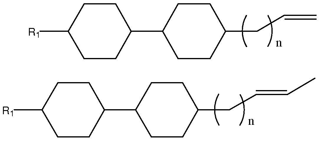 式 IV, 其中, 所述 1^表示具有 1~10个碳原子的垸基, 11为 1~10。
2. 如权利要求 1所述的液晶组合物,其中,所述液晶分子为垂直配向的液晶分 子。
3. 如权利要求 1所述的液晶组合物,其中,所述液晶组成物为滴下式注入技术 的液晶组成
4. 一种液晶组合物, 用于制作液晶面板, 其中, 所述液晶组合物包含:
至少一种聚合性单体; 至少一种液晶分子; 以及至少一种稀释剂;
所述稀释剂为包含一个或多个烯基的液晶化合物;
I表示:

所述 A基团为硬核, 以下述分子通式 II表

其中, 所述 X选自 H、 F或 CH3中的一种。
5. 如权利要求 4所述的液晶组合物,其中,所述液晶分子为垂直配向的液晶分 子。
6. 如权利要求 4所述的液晶组合物,其中,所述液晶组成物为滴下式注入技术 的液晶组成物。
7.一种液晶面板, 包括分别配置有配向膜的一第一基板和一第二基板, 其中, 在所述第一基板和第二基板的配向膜表面上扩散分布有一种如权利要求 1~3 中任一所述液晶组合物。
8. 如权利要求 7所述的液晶面板, 其中, 所述配向膜为垂直配向型的配向膜。
9. 如权利要求 7所述的液晶面板, 其中, 所述第一基板为彩色滤光片基板, 所 述第二基板为薄膜晶体管阵列基板。
10. 如权利要求 7所述的液晶面板, 其中, 所述液晶组成物为滴下式注入技术
Priority Applications (1)
| Application Number | Priority Date | Filing Date | Title |
|---|---|---|---|
| US13/702,048 US8845925B2 (en) | 2012-10-29 | 2012-11-14 | Liquid crystal composition and liquid crystal panel |
Applications Claiming Priority (2)
| Application Number | Priority Date | Filing Date | Title |
|---|---|---|---|
| CN2012104208391A CN102936504A (zh) | 2012-10-29 | 2012-10-29 | 液晶组合物与液晶面板 |
| CN201210420839.1 | 2012-10-29 |
Publications (1)
| Publication Number | Publication Date |
|---|---|
| WO2014067176A1 true WO2014067176A1 (zh) | 2014-05-08 |
Family
ID=47695428
Family Applications (1)
| Application Number | Title | Priority Date | Filing Date |
|---|---|---|---|
| PCT/CN2012/084558 Ceased WO2014067176A1 (zh) | 2012-10-29 | 2012-11-14 | 液晶组合物与液晶面板 |
Country Status (2)
| Country | Link |
|---|---|
| CN (1) | CN102936504A (zh) |
| WO (1) | WO2014067176A1 (zh) |
Families Citing this family (2)
| Publication number | Priority date | Publication date | Assignee | Title |
|---|---|---|---|---|
| KR101643209B1 (ko) * | 2013-09-20 | 2016-07-27 | 디아이씨 가부시끼가이샤 | 액정 표시 소자 및 그 제조 방법 |
| CN110317148B (zh) * | 2019-06-27 | 2022-05-03 | Tcl华星光电技术有限公司 | 反应型单体和液晶组合物及液晶显示面板 |
Citations (3)
| Publication number | Priority date | Publication date | Assignee | Title |
|---|---|---|---|---|
| CN101144944A (zh) * | 2007-11-08 | 2008-03-19 | 友达光电股份有限公司 | 用于高分子取向工序的液晶混合物以及液晶显示装置 |
| CN101671252A (zh) * | 2009-10-20 | 2010-03-17 | 友达光电股份有限公司 | 应用于显示面板的可聚合单体以及液晶材料 |
| WO2011004519A1 (ja) * | 2009-07-08 | 2011-01-13 | シャープ株式会社 | 液晶表示パネルおよびその製造方法 |
Family Cites Families (5)
| Publication number | Priority date | Publication date | Assignee | Title |
|---|---|---|---|---|
| CN102701983B (zh) * | 2006-08-11 | 2015-10-28 | 友达光电股份有限公司 | 单体及应用其制造液晶显示面板的方法 |
| DE102008056221A1 (de) * | 2007-11-30 | 2009-06-04 | Merck Patent Gmbh | Polymerisierbare Verbindungen |
| US8283000B2 (en) * | 2008-02-22 | 2012-10-09 | Adeka Corporation | Liquid crystal composition containing polymerizable compound and liquid crystal display using the liquid crystal composition |
| JP5545516B2 (ja) * | 2009-09-25 | 2014-07-09 | Dic株式会社 | 重合性化合物 |
| JP5593890B2 (ja) * | 2010-07-06 | 2014-09-24 | Dic株式会社 | 液晶組成物および液晶デバイス |
-
2012
- 2012-10-29 CN CN2012104208391A patent/CN102936504A/zh active Pending
- 2012-11-14 WO PCT/CN2012/084558 patent/WO2014067176A1/zh not_active Ceased
Patent Citations (3)
| Publication number | Priority date | Publication date | Assignee | Title |
|---|---|---|---|---|
| CN101144944A (zh) * | 2007-11-08 | 2008-03-19 | 友达光电股份有限公司 | 用于高分子取向工序的液晶混合物以及液晶显示装置 |
| WO2011004519A1 (ja) * | 2009-07-08 | 2011-01-13 | シャープ株式会社 | 液晶表示パネルおよびその製造方法 |
| CN101671252A (zh) * | 2009-10-20 | 2010-03-17 | 友达光电股份有限公司 | 应用于显示面板的可聚合单体以及液晶材料 |
Also Published As
| Publication number | Publication date |
|---|---|
| CN102936504A (zh) | 2013-02-20 |
Similar Documents
| Publication | Publication Date | Title |
|---|---|---|
| CN104252066B (zh) | 液晶聚合物组分、液晶显示装置及其制造方法 | |
| WO2017181466A1 (zh) | 液晶材料、液晶显示面板的制作方法及液晶显示面板 | |
| WO2018120325A1 (zh) | 垂直取向剂材料 | |
| TWI553040B (zh) | Silicon liquid crystal alignment agent, liquid crystal alignment film and liquid crystal display components | |
| CN106085464B (zh) | 配向膜材料、液晶显示面板的制作方法及液晶显示面板 | |
| CN105885872B (zh) | 液晶材料、液晶显示面板及液晶显示面板的制作方法 | |
| KR101829478B1 (ko) | 액정 배향제, 액정 배향막 및 액정 표시 소자 | |
| US10073300B2 (en) | Display panel and display device | |
| CN105974675B (zh) | 柔性显示面板及其制作方法 | |
| WO2018028019A1 (zh) | 一种液晶介质混合物及液晶显示面板 | |
| CN105481889B (zh) | 反应型垂直取向有机硅材料及液晶显示面板的制作方法 | |
| CN106188540B (zh) | 配向膜材料及配向膜的制作方法、液晶显示面板及其制作方法 | |
| WO2014075311A1 (zh) | 光反应型单体及其液晶组合物与液晶面板 | |
| WO2014067176A1 (zh) | 液晶组合物与液晶面板 | |
| CN102732264B (zh) | 一种液晶活性单体及液晶面板 | |
| CN104054019B (zh) | 硅系液晶取向剂、液晶取向膜及液晶显示元件 | |
| CN103827155B (zh) | 聚合性液晶组合物和取向膜 | |
| US20040201797A1 (en) | Process for preparing positive-negative blended optical retardation film, positive-negative blended optical retardation film, and liquid crystal display element and liquid crystal display device using the same | |
| WO2014075261A1 (zh) | 感光单体及液晶面板 | |
| WO2014089821A1 (zh) | 液晶组成物、液晶配向混合物及液晶面板 | |
| CN110317148B (zh) | 反应型单体和液晶组合物及液晶显示面板 | |
| KR100430120B1 (ko) | 박막형성용 화학흡착물질 및 그 제조방법 및 그 용도 | |
| CN108034434A (zh) | 热聚合自取向液晶材料及液晶显示面板的制作方法 | |
| US8845925B2 (en) | Liquid crystal composition and liquid crystal panel | |
| US9725650B2 (en) | Reactive monomer, a liquid crystal panel and an electronic equipment |
Legal Events
| Date | Code | Title | Description |
|---|---|---|---|
| WWE | Wipo information: entry into national phase |
Ref document number: 13702048 Country of ref document: US |
|
| 121 | Ep: the epo has been informed by wipo that ep was designated in this application |
Ref document number: 12887356 Country of ref document: EP Kind code of ref document: A1 |
|
| NENP | Non-entry into the national phase |
Ref country code: DE |
|
| 122 | Ep: pct application non-entry in european phase |
Ref document number: 12887356 Country of ref document: EP Kind code of ref document: A1 |