WO2014050308A1 - 回折光学素子ならびに回折光学素子の製造方法および製造装置 - Google Patents
回折光学素子ならびに回折光学素子の製造方法および製造装置 Download PDFInfo
- Publication number
- WO2014050308A1 WO2014050308A1 PCT/JP2013/070992 JP2013070992W WO2014050308A1 WO 2014050308 A1 WO2014050308 A1 WO 2014050308A1 JP 2013070992 W JP2013070992 W JP 2013070992W WO 2014050308 A1 WO2014050308 A1 WO 2014050308A1
- Authority
- WO
- WIPO (PCT)
- Prior art keywords
- optical element
- diffractive optical
- polymer material
- material layer
- dye
- Prior art date
- Legal status (The legal status is an assumption and is not a legal conclusion. Google has not performed a legal analysis and makes no representation as to the accuracy of the status listed.)
- Ceased
Links
Images






Classifications
-
- G—PHYSICS
- G02—OPTICS
- G02B—OPTICAL ELEMENTS, SYSTEMS OR APPARATUS
- G02B5/00—Optical elements other than lenses
- G02B5/18—Diffraction gratings
- G02B5/1847—Manufacturing methods
- G02B5/1857—Manufacturing methods using exposure or etching means, e.g. holography, photolithography, exposure to electron or ion beams
-
- G—PHYSICS
- G03—PHOTOGRAPHY; CINEMATOGRAPHY; ANALOGOUS TECHNIQUES USING WAVES OTHER THAN OPTICAL WAVES; ELECTROGRAPHY; HOLOGRAPHY
- G03F—PHOTOMECHANICAL PRODUCTION OF TEXTURED OR PATTERNED SURFACES, e.g. FOR PRINTING, FOR PROCESSING OF SEMICONDUCTOR DEVICES; MATERIALS THEREFOR; ORIGINALS THEREFOR; APPARATUS SPECIALLY ADAPTED THEREFOR
- G03F7/00—Photomechanical, e.g. photolithographic, production of textured or patterned surfaces, e.g. printing surfaces; Materials therefor, e.g. comprising photoresists; Apparatus specially adapted therefor
- G03F7/20—Exposure; Apparatus therefor
- G03F7/2051—Exposure without an original mask, e.g. using a programmed deflection of a point source, by scanning, by drawing with a light beam, using an addressed light or corpuscular source
- G03F7/2053—Exposure without an original mask, e.g. using a programmed deflection of a point source, by scanning, by drawing with a light beam, using an addressed light or corpuscular source using a laser
-
- G—PHYSICS
- G03—PHOTOGRAPHY; CINEMATOGRAPHY; ANALOGOUS TECHNIQUES USING WAVES OTHER THAN OPTICAL WAVES; ELECTROGRAPHY; HOLOGRAPHY
- G03H—HOLOGRAPHIC PROCESSES OR APPARATUS
- G03H1/00—Holographic processes or apparatus using light, infrared or ultraviolet waves for obtaining holograms or for obtaining an image from them; Details peculiar thereto
- G03H1/02—Details of features involved during the holographic process; Replication of holograms without interference recording
- G03H1/024—Hologram nature or properties
- G03H1/0244—Surface relief holograms
-
- G—PHYSICS
- G03—PHOTOGRAPHY; CINEMATOGRAPHY; ANALOGOUS TECHNIQUES USING WAVES OTHER THAN OPTICAL WAVES; ELECTROGRAPHY; HOLOGRAPHY
- G03H—HOLOGRAPHIC PROCESSES OR APPARATUS
- G03H1/00—Holographic processes or apparatus using light, infrared or ultraviolet waves for obtaining holograms or for obtaining an image from them; Details peculiar thereto
- G03H1/04—Processes or apparatus for producing holograms
- G03H1/08—Synthesising holograms, i.e. holograms synthesized from objects or objects from holograms
- G03H1/0891—Processes or apparatus adapted to convert digital holographic data into a hologram
-
- G—PHYSICS
- G03—PHOTOGRAPHY; CINEMATOGRAPHY; ANALOGOUS TECHNIQUES USING WAVES OTHER THAN OPTICAL WAVES; ELECTROGRAPHY; HOLOGRAPHY
- G03H—HOLOGRAPHIC PROCESSES OR APPARATUS
- G03H2224/00—Writing means other than actinic light wave
- G03H2224/06—Thermal or photo-thermal means
-
- G—PHYSICS
- G03—PHOTOGRAPHY; CINEMATOGRAPHY; ANALOGOUS TECHNIQUES USING WAVES OTHER THAN OPTICAL WAVES; ELECTROGRAPHY; HOLOGRAPHY
- G03H—HOLOGRAPHIC PROCESSES OR APPARATUS
- G03H2260/00—Recording materials or recording processes
- G03H2260/30—Details of photosensitive recording material not otherwise provided for
- G03H2260/33—Having dispersed compound
-
- G—PHYSICS
- G03—PHOTOGRAPHY; CINEMATOGRAPHY; ANALOGOUS TECHNIQUES USING WAVES OTHER THAN OPTICAL WAVES; ELECTROGRAPHY; HOLOGRAPHY
- G03H—HOLOGRAPHIC PROCESSES OR APPARATUS
- G03H2260/00—Recording materials or recording processes
- G03H2260/50—Reactivity or recording processes
- G03H2260/61—Producing material deformation
Definitions
- the present invention relates to a diffractive optical element that can be used as an image display device, a security element, an optical filter element, and the like, and a manufacturing method and a manufacturing apparatus of the diffractive optical element.
- Patent Document 1 a method for manufacturing a diffractive optical element
- Patent Document 2 a method of manufacturing a diffractive optical element by forming a fine uneven shape by laser ablation by irradiating the surface of a polymer material with laser light.
- the diffractive optical element according to one embodiment of the present invention includes a polymer material layer, and the polymer material layer is dispersed in the polymer material and the polymer material layer, or the polymer material layer And a dye which is covalently bonded to a molecular material, and a diffractive optical element pattern having dot-like openings and / or convex portions is arranged at the interface of the polymer material layer.
- the dye contained in the polymer material layer absorbs laser light, thereby giving energy to the polymer material layer with high efficiency and opening the interface at the polymer material layer. It is also possible to form a diffractive optical element pattern by forming convex portions. Therefore, it is not necessary to perform etching, and it can be easily manufactured in a short irradiation time. Further, since the openings and / or convex portions are formed by deforming the interface rather than peeling the material as in laser ablation, it is possible to form a diffractive optical element pattern that can be finely controlled in gradation. .
- the opening referred to in the present invention may be a bottomed recess or may penetrate the polymer material layer.
- the dye may include a one-photon absorption dye.
- the dye contains a one-photon absorption dye, it can be processed with a low energy laser such as a semiconductor laser.
- the dye may include a multiphoton absorbing dye.
- a diffractive optical element having high transmittance in the visible wavelength region can be obtained.
- the diffractive optical element described above can have a support that supports the polymer material layer. By providing the support, it is possible to reduce the cost by thinning the polymer material layer.
- the diffractive optical element described above preferably includes a cover layer on the side where the openings and / or convex portions of the polymer material layer are arranged.
- the cover layer is provided on the side where the openings and / or convex portions are arranged, the functions of the diffractive optical element can be maintained by protecting the openings and / or convex portions.
- a multi-value diffractive optical element pattern is formed by the plurality of types of openings and / or projections. It can be set as a structure. By configuring the multi-value diffractive optical element pattern in this way, it is possible to enhance the function of the diffractive optical element, such as removing unnecessary diffraction images. In order to change the depth or height of the opening and / or the convex portion, it is only necessary to adjust the irradiation time of the laser beam. Therefore, a highly functional diffractive optical element can be easily manufactured. it can.
- the dye has an absorption wavelength band of mainly 450 nm or less and a light transmittance of a wavelength of 450 to 800 nm of 50% or more. That is, the dye mainly absorbs light in a wavelength region of 450 nm or less, whereby a diffractive optical element that is relatively colorless (highly transmissive in the visible wavelength region) can be obtained.
- a method for manufacturing a diffractive optical element comprising: preparing a polymer material layer having a polymer material in which a dye is dispersed or a polymer material having a dye covalently bonded; Dot-shaped openings and / or protrusions that form a diffractive optical element pattern at the interface by irradiating laser light having a wavelength that is absorbed by the dye in the vicinity to deform the interface and performing this irradiation at the interface in a predetermined pattern It is characterized by forming.
- the irradiation time of the laser beam for forming one opening or convex portion is 120 ⁇ sec or less.
- the diffractive optical element can be manufactured at high speed.
- the reflected light from the interface is detected by the sensor during the irradiation of the laser light, and the focal position of the laser light is adjusted to a predetermined position based on the output signal of the sensor.
- the focal position based on the reflected light from the interface it is possible to obtain a diffractive optical element with desired performance by aligning the size of the opening or the recess.
- a diffractive optical element manufacturing apparatus for forming a diffractive optical element pattern on a polymer material layer having a polymer material in which a dye is dispersed or a polymer material to which a dye is covalently bonded.
- the diffractive optical element manufacturing apparatus includes a light source that emits laser light having a wavelength that is absorbed by the dye, a deflector that deflects the laser light emitted from the light source, and a laser beam deflected by the deflector as a polymer material.
- An image forming optical system for forming an image near the interface of the layer, and a control device for controlling the output of the light source and the deflector.
- the control device is a dot that forms a diffractive optical element pattern at the interface of the polymer material layer.
- the output of the light source is changed in synchronism with the scanning of the laser beam on the interface of the polymer material layer by controlling the deflector so as to form an opening and / or a convex portion.
- an optical diffractive element can be manufactured by changing the output of a light source while scanning a laser beam with a deflector and forming an opening and / or a convex portion at the interface of the polymer material layer. it can. Further, since the diffractive optical element pattern is formed at the interface by scanning the laser beam on the interface, it is not necessary to use a mask as in the prior art. Furthermore, in this manufacturing apparatus, since the diffractive optical element pattern is formed by scanning the laser beam on the interface with a deflector, it is not necessary to move the polymer material layer during processing. The manufacturing apparatus irradiates the polymer material layer containing the dye with laser light to form openings and / or projections, so that the output of the laser light can be reduced and the processing can be performed at high speed. .
- the imaging optical system includes an objective lens and at least two condenser lenses.
- the irradiation time of the laser light for forming one opening or convex portion is 120 ⁇ sec or less.
- the diffractive optical element can be manufactured at high speed.
- the imaging optical system preferably includes an objective lens, and the objective lens preferably has a numerical aperture of 0.13 or more.
- the objective lens preferably has a numerical aperture of 0.13 or more.
- the manufacturing apparatus described above further includes a sensor that detects the laser light reflected at the interface, and the control apparatus controls the imaging optical system based on the output signal of the sensor to adjust the focal position of the laser light to a predetermined position. It is desirable to be configured as follows.
- the size of the opening or the concave portion is made uniform, and a diffractive optical element having a desired performance can be obtained.
- the wavelength of the laser light emitted from the light source is preferably 450 nm or less.
- a dye that does not absorb much visible light can be used as a dye, so that the diffractive optical element can be made relatively colorless.
- a transport device that moves the polymer material layer relative to the laser beam.
- a plurality of diffractive optical elements can be continuously manufactured by moving the polymer material layer by the transport device.
- the diffractive optical element can be easily manufactured in a short time.
- a diffractive optical element pattern is formed at the interface by scanning the interface with laser light, so that it is not necessary to use a mask as in the prior art.
- the diffractive optical element pattern is formed by scanning the laser beam on the interface with the deflector, and therefore it is not necessary to move the polymer material layer during processing.
- FIG. 5 is a simulation result of a reproduced image using the (a) design original image, (b) phase pattern, and (c) (b) phase pattern in the diffractive optical element of Example 1 displaying an image as a diffraction image.
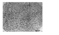
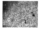
- . 2 is a laser microscope image of the diffractive optical element of Example 1.
- FIG. 17 is a laser microscope image of the diffractive optical element of Example 1 in which a part of the visual field in FIG. 16 is enlarged.
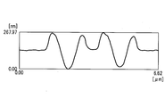
- 2 is a cross-sectional profile of a concave portion of the diffractive optical element of Example 1.
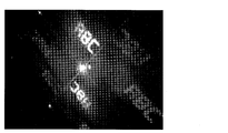
- 2 is a reproduced image using the diffractive optical element of Example 1.
- FIG. It is the reproduction
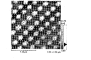
- 4 is an atomic force microscope image of the diffractive optical element of Example 3.
- FIG. 10 is a cross-sectional profile of a convex portion of a diffractive optical element of Example 3.
- the diffractive optical element E of the present invention is a diffractive optical element pattern formed by forming fine dot-shaped openings and / or convex portions in a predetermined range of a sheet-like member.
- the pattern area PA on which the diffractive optical element pattern is formed has a square as an example, but the shape of the pattern area PA is not particularly limited.
- the diffractive optical element E an element that obtains a diffracted image that becomes a predetermined image by applying a laser beam is exemplified.
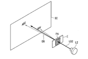
- the diffractive optical element E is arranged in the order of the reproduction laser L2, the diffractive optical element E, and the screen SC, and emits the reproduction laser light LB2 from the reproduction laser L2.
- the laser beam LB2 for use is passed through the pattern area PA to obtain the diffracted light DB.
- the diffracted light DB displays a predetermined image by irradiating the pattern region PA with the reproduction laser beam LB2.
- the diffractive optical element E can also be used as shown in FIG.
- the reproducing laser L2, the screen SC, and the diffractive optical element E are arranged in this order, and the hole SC1 is formed in the screen SC. Then, the reproducing laser beam LB2 emitted from the reproducing laser L2 is applied to the pattern area PA of the diffractive optical element E through the hole SC1. In this way, the reproduction laser beam LB2 is diffracted by the diffractive optical element pattern while being reflected at the interface where the diffractive optical element pattern of the diffractive optical element E is formed, and displays a predetermined image on the screen SC. be able to.
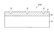
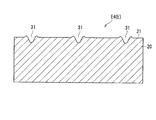
- the diffractive optical element E As shown in FIG. 4, the diffractive optical element E according to the first embodiment has a structure composed of two layers in which a polymer material layer 20 is provided on a support 10.
- the support 10 is a member for supporting the polymer material layer 20.
- the material of the support 10 is not particularly limited, but is made of a material that can transmit the reproducing laser beam LB2 of the reproducing laser L2 as an example because the reproducing laser beam LB2 is transmitted therethrough.
- the support 10 may be a member that is opaque to the reproduction laser beam LB2.
- the support 10 may be a metal plate, and the surface of the support 10 on the polymer material layer 20 side may be used as a reflection surface.
- the thickness of the support 10 is not particularly limited as long as it has sufficient mechanical properties to support the polymer material layer 20, and may be a film of about 1 mm or less, for example, about 1 mm or more. A plate-like member may be used.
- the polymer material layer 20 has a diffractive optical element pattern formed by dot-like openings and / or convex portions (hereinafter, sometimes referred to as “lattice points”) at the interface, here the interface 21 with the air layer. It is a layer to be formed.
- a plurality of recesses 31 are formed as an example of the opening.
- the concave portions 31 in FIG. 4 are dot-like when viewed in plan, and all have substantially the same depth and diameter.
- the diffractive optical element pattern is designed according to a desired reproduced image, and is, for example, a pattern like the laser microscope image of FIGS.
- the polymer material layer 20 has a dispersed dye or a dye covalently bonded to the polymer material in the polymer material layer 20.
- the dye When the dye is covalently bonded to the polymer material, it prevents the precipitation and elution of the dye due to long-term storage, and can reduce the time-dependent change in optical properties such as transmittance and reflectance, and has excellent long-term storage
- a diffractive optical element can be constructed.
- the dye herein can include a one-photon absorbing dye and / or a multi-photon absorbing dye.
- a one-photon absorption dye When a one-photon absorption dye is included, it can be processed with a low energy laser such as a semiconductor laser.
- a multiphoton absorbing dye when a multiphoton absorbing dye is included, the diffractive optical element E1 having high transparency in the visible wavelength region can be configured.
- the one-photon absorption dye is preferably a one-photon absorption compound that does not have a linear absorption band at the wavelength of the reproduction laser beam LB2, and the multiphoton absorption dye does not have a linear absorption band at the wavelength of the reproduction laser light LB2.
- a multiphoton absorbing compound is preferred.
- the absorptance (one-photon absorptance) of the polymer material layer 20 with respect to laser light (recording laser light) for forming lattice points is desirably 5% or more per 1 ⁇ m thickness, and is 10% or more. Is more desirable.
- the higher the absorptance the faster the temperature of the polymer material can be increased when the recording laser light is irradiated, the diffractive optical element E1 can be formed in a short time, and a low energy laser light source is used. be able to.
- the formation method of the polymer material layer 20 is not particularly limited, but the polymer material layer 20 can be formed by spin coating or blade coating using a solution obtained by dissolving a dye material and a polymer material in a solvent.
- a solvent As the solvent at this time, dichloromethane, chloroform, methyl ethyl ketone (MEK), acetone, methyl isobutyl ketone (MIBK), toluene, hexane, or the like can be used.
- Polymer materials used for the polymer material layer 20 include polyvinyl acetate (PVAc), polymethyl methacrylate (PMMA), polyethyl methacrylate, polybutyl methacrylate, polybenzyl methacrylate, polyisobutyl methacrylate, polycyclohexyl methacrylate, polycarbonate (PC ), Polystyrene (PS), polyvinyl chloride (PVC), polyvinyl alcohol (PVA), and the like.
- the range of the molecular weight Mw of the polymer material (or polymer material to which a dye is covalently bonded) in the polymer material layer 20 is preferably 10,000 to 1,000,000.
- the molecular weight Mw can be measured by gel permeation chromatography (GPC).
- the glass transition point Tg of the polymer material is preferably 60 ° C. or higher, and more preferably 100 ° C. or higher.
- the glass transition point Tg of the polymer material is preferably 300 ° C. or lower in order to realize high-speed processing of lattice points.
- the dye dispersed in the polymer material or the dye covalently bonded to the polymer material is a methine dye (cyanine dye, hemicyanine dye, styryl dye, oxonol dye, merocyanine dye, etc.) as long as it is a one-photon absorption dye.
- Macrocyclic dyes phthalocyanine dyes, naphthalocyanine dyes, porphyrin dyes, etc.
- azo dyes including azo metal chelate dyes
- arylidene dyes complex dyes, coumarin dyes, azole derivatives, triazine derivatives, benzotriazole derivatives, benzophenone derivatives, phenoxy Sazine derivatives, phenothiazine derivatives, 1-aminobutadiene derivatives, cinnamic acid derivatives, quinophthalone dyes, and the like
- azo dyes including azo metal chelate dyes
- arylidene dyes complex dyes
- coumarin dyes coumarin dyes
- azole derivatives triazine derivatives
- benzotriazole derivatives benzophenone derivatives
- phenoxy Sazine derivatives phenothiazine derivatives
- 1-aminobutadiene derivatives 1-aminobutadiene derivatives
- triazine derivatives, benzotriazole derivatives, and benzophenone derivatives are ultraviolet absorbing dyes, the absorption wavelength band is mainly 450 nm or less, and the light transmittance at a wavelength of 450 to 800 nm is 50% or more. Therefore, when these dyes are used, light in a wavelength region of 450 nm or less is mainly absorbed, so that a relatively colorless diffractive optical element E1 can be configured.
- the dye compound is not particularly limited as long as it does not have a linear absorption band at the wavelength of the reproduction laser beam LB2.
- the dye compound is represented by the following general formula (1). Examples thereof include compounds having a structure.
- X and Y each represent a substituent having a Hammett's sigma para value ( ⁇ p value) of zero or more, which may be the same or different, and n represents an integer of 1 to 4.
- R represents a substituent, which may be the same or different, and m represents an integer of 0 to 4.
- X and Y are those having a positive ⁇ p value in the Hammett formula, so-called electron-withdrawing groups, and preferably, for example, a trifluoromethyl group, a heterocyclic group, a halogen atom, a cyano group Nitro group, alkylsulfonyl group, arylsulfonyl group, sulfamoyl group, carbamoyl group, acyl group, acyloxy group, alkoxycarbonyl group, etc., more preferably trifluoromethyl group, cyano group, acyl group, acyloxy group, Or an alkoxycarbonyl group, and most preferably a cyano group or a benzoyl group.
- an alkylsulfonyl group, an arylsulfonyl group, a sulfamoyl group, a carbamoyl group, an acyl group, an acyloxy group, and an alkoxycarbonyl group are further added for various purposes in addition to imparting solubility to a solvent. It may have a substituent, and preferred examples of the substituent include an alkyl group, an alkoxy group, an alkoxyalkyl group, and an aryloxy group.
- n is preferably 2 or 3, most preferably 2. As n becomes 5 or more, linear absorption comes out on the longer wavelength side, and non-resonant two-photon absorption recording using recording light in a wavelength region shorter than 700 nm becomes impossible.
- R represents a substituent, and the substituent is not particularly limited, and specific examples include an alkyl group, an alkoxy group, an alkoxyalkyl group, and an aryloxy group.
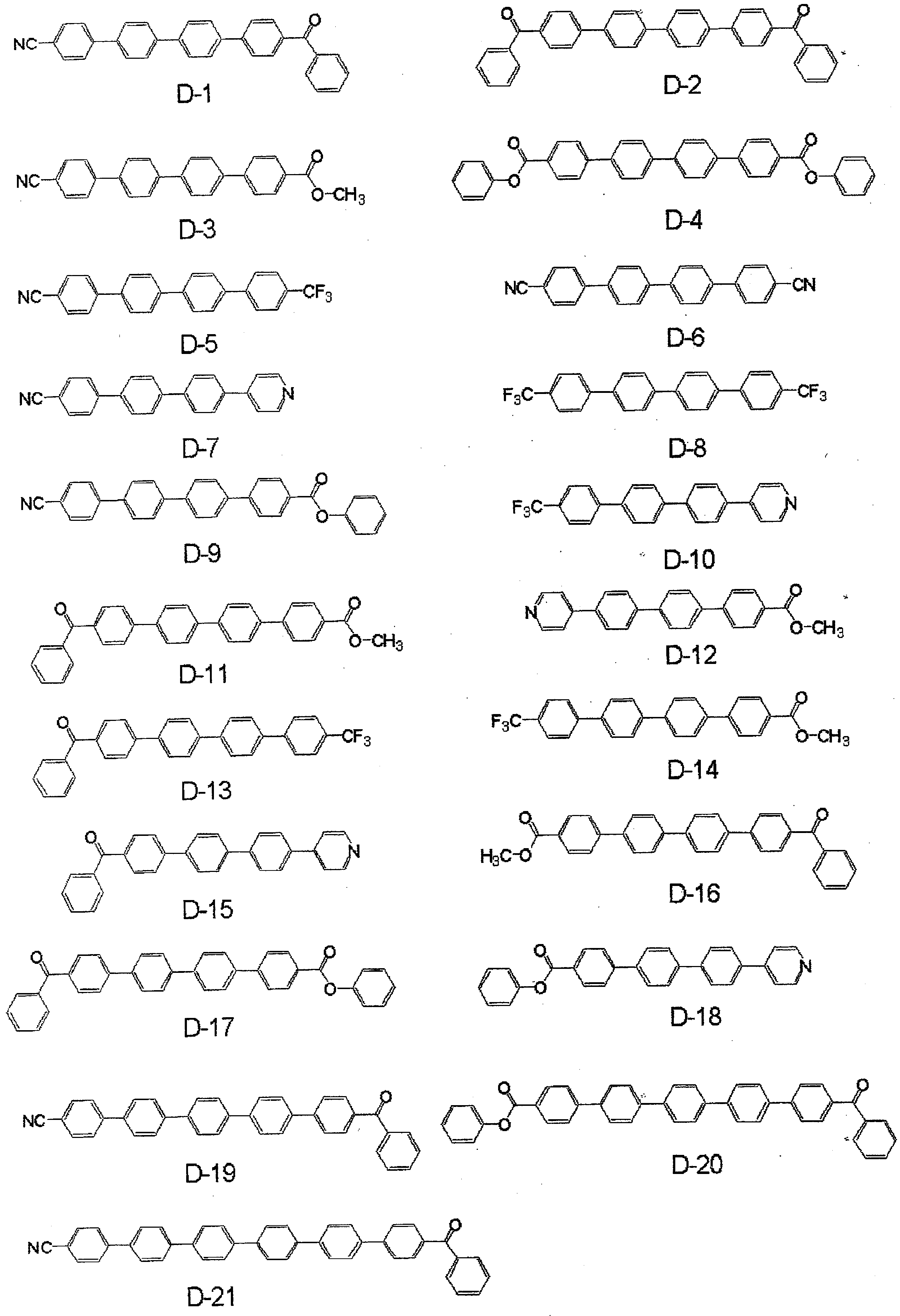
- Specific examples of the compound having the structure represented by the general formula (1) are not particularly limited, but compounds represented by the following chemical structural formulas D-1 to D-21 can be used.
- polymer material to which the dye is covalently bonded for example, a compound represented by the following general formula (2) can be used.
- Y represents a substituent in which both Hammett's sigma para value ( ⁇ p value) has a value of zero or more, and X also represents the same kind of substituent.
- N represents an integer of 1 to 4
- R1, R2, and R3 represent substituents, which may be the same or different
- l represents 1 or more
- m represents an integer of 0 to 4.
- the concave portion 31 can be formed by condensing and irradiating the recording material laser beam on the polymer material layer 20, and the diffractive optical element E1 can be manufactured.
- the dye contained in the polymer material layer 20 is made to absorb the recording laser light, whereby energy can be given to the polymer material layer 20 with high efficiency, and the diffractive optical element E1 can be manufactured in a short time.
- the diffractive optical element E1 can be manufactured in a short time because etching is not necessary at the time of manufacture.
- the recess 31 is formed by deforming the interface rather than peeling the material as in laser ablation, a fine and gradation-controllable optical element pattern can be formed. Further, by supporting the polymer material layer 20 on the support 10, the polymer material layer 20 can be thinned, and the cost can be reduced.
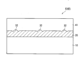
- the diffractive optical element E2 of the second embodiment includes a support 10 and a polymer material layer 20, and lattice points on the opposite side of the polymer material layer 20 from the support 10 are arranged.
- a cover layer 41 is provided on the provided side.
- the cover layer 41 is for protecting the shape of the lattice points mechanically or chemically.
- the configuration of the cover layer 41 is not particularly limited as long as the lattice points are not adversely affected.
- the cover layer 41 can be provided by applying and curing an ultraviolet curable resin.
- the cover layer 41 may be configured by attaching a film (such as polycarbonate) with an adhesive.
- the diffractive optical element E2 of the second embodiment has a lattice point constituted by a convex portion 32. Whether the lattice point is an opening or a convex portion is determined by the absorption energy (output, irradiation time and absorption rate) of the polymer material layer 20 when the recording laser beam is irradiated. If it is large, it tends to be an opening.
- the cover layer 41 protects the lattice points and can be stored for a long time.
- the lattice points are preferably formed after the cover layer 41 is provided. By doing so, the shape of the lattice points is not disturbed when the cover layer 41 is provided, and the presence of air or the like between the cover layer 41 and the polymer material layer 20 can be suppressed.
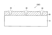
- the diffractive optical element E ⁇ b> 3 has a form in which the lattice point is a hole 33 penetrating the polymer material layer 20 with respect to the first embodiment.
- Such holes 33 may be formed by thinly forming the polymer material layer 20 and exposing the polymer material layer 20 with large energy when forming lattice points. Even if such holes 33 are used as lattice points, the function of the diffractive optical element can be exhibited as in the first embodiment, and it can be manufactured easily and in a short time.
- the dye of the polymer material layer 20 absorbs a lot of light in the visible wavelength region (for example, 50% or more).
- the reproduction laser beam LB2 can be passed through the hole 33, and the diffracted light of the light that has passed through the hole 33 can be used.
- the diffractive optical element E4 according to the fourth embodiment is obtained by eliminating the support 10 from the first embodiment, and instead of providing the support 10, the thickness of the polymer material layer 20 is increased. And the shape of the diffractive optical element E4 is maintained.
- the polymer material layer 20 may be a film of about 1 mm or less or a plate-shaped member of about 1 mm or more.
- the manufacturing process can be simplified by omitting the support.
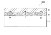
- the diffractive optical element E5 according to the fifth embodiment is different from the first embodiment in that the diffractive optical element E5 has lattice points on the inner interface on the support side instead of the interface with the air of the polymer material layer 20.
- a recess 31 is formed.
- an adhesive that is a layer softer than the polymer material layer 20 for example, having a low glass transition point Tg) between the support 10 and the polymer material layer 20 so that the inner interface is easily deformed.
- Layer 42 is interposed.
- the recording laser beam may be condensed and irradiated near the inner interface.
- the lattice points may be convex when viewed from the polymer material layer 20 (may project from the polymer material layer 20).
- the shape of the lattice points can be changed without providing the cover layer 41 separately. Can be protected.
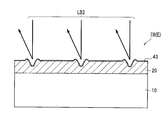
- the diffractive optical element E6 is different from the first embodiment in that a reflective layer 43 is provided on the outer surface of the polymer material layer 20.
- the reflective layer 43 may be a metal thin film, or may be a layer made of a material having a refractive index significantly different from that of the polymer material layer 20.
- the diffractive optical element E6 having such a configuration, as indicated by an arrow in FIG. 9, the reproducing laser beam LB2 is reflected by the reflective layer 43, and the reproducing laser beam LB2 is incident on the diffractive optical element E6.
- a reproduced image can be formed.
- the reproduction laser beam LB2 is irradiated from the outside (upper side of the drawing) of the reflective layer 43, but the reproduction laser beam LB2 is irradiated from the opposite side (lower side of the drawing). I do not care.
- the diffractive optical element E7 according to the seventh embodiment is different from the first embodiment in that the grating point is not limited to the concave portion 31 having a constant depth, but different depths, for example, the concave portion 31.
- the deep concave portions 31B are mixed and arranged. In order to make the depths of the recesses different, it is only necessary to make the irradiation time of the recording laser light different during manufacture. When the recording laser light is irradiated for a short time, a shallow concave portion is formed, and when irradiated for a long time, a deep concave portion is formed.
- the concave portions 31 and the concave portions 31B having different depths when there are the concave portions 31 and the concave portions 31B having different depths, when the reproduction laser beam LB2 is diffracted at each lattice point during use, the optical path length of the diffracted light is different at each lattice point.
- the diffraction angle which is the traveling direction determined by the interference of the reproduction laser beam LB2 diffracted by a plurality of lattice points, can be adjusted.
- the multi-valued diffraction grating using the concave portion 31 and the concave portion 31B can give variations to the image, such as fading the inverted image or the secondary diffraction image.
- the recesses 31 and the recesses 31B having two kinds of depths are mixed in the lattice point is illustrated here, the recesses having three or more kinds of depths may be mixed.
- the diffractive optical element E8 according to the eighth embodiment is obtained by arranging not only the concave portions 31 but also the convex portions 32 in the lattice points in the first embodiment.
- the concave portion 31 and the convex portion 32 are present, as in the seventh embodiment, when the reproduction laser beam LB2 is diffracted at each lattice point during use, the optical path length of the light diffracted at each lattice point is set. Since the difference is made, it is possible to adjust the diffraction angle, which is the traveling direction determined by the interference of the reproduction laser beam LB2 diffracted by a plurality of lattice points. For this reason, the multi-valued diffraction grating using the concave portion 31 and the convex portion 32 can give variations to the image, such as fading the inverted image or the secondary diffraction image.
- a structured diffraction grating may be configured.
- a diffractive optical element pattern may be formed.
- diffractive optical element E Although various forms of the diffractive optical element E have been described above, the features of the diffractive optical elements E can be applied in combination with each other.
- the manufacturing apparatus 50 mainly includes a recording laser 51 as a light source, a deflector 52, a stage 57, an imaging optical system 60, and a control device 59.
- the recording laser 51 is a laser that emits the recording laser beam LB1, and is preferably a semiconductor laser.
- the wavelength of the recording laser beam LB1 is a wavelength that is absorbed by the dye in the polymer material layer 20 (one-photon absorption and / or multiphoton absorption), and the wavelength of the reproducing laser beam LB2 used when the diffractive optical element E is used. It is desirable to be different from the wavelength. Accordingly, since the diffractive optical element E is suppressed from being heated by the reproducing laser beam LB2 during reproduction, the reproducing laser beam LB2 having a large output can be used during reproduction. In particular, when the diffractive optical element E for image display is manufactured, it is desirable that the diffractive optical element E has high transparency in the visible wavelength range. Therefore, the recording laser 51 has a wavelength of 450 nm or less. It is desirable that the laser beam LB1 is emitted.
- the recording laser 51 is preferably a short wavelength laser capable of reducing the spot size of the recording laser beam LB1, and in particular, 400 to 410 nm.
- the semiconductor laser may be preferable.
- the recording laser 51 may have an output with an average power of 10 mW or more, more preferably 100 mW or more. Note that, when a multiphoton absorption dye is used as the dye in the polymer material layer 20, a wavelength without linear absorption is used, so that it is easy to make a diffractive optical element E that is particularly highly transparent in the visible wavelength region.
- the deflector 52 is a device that deflects the traveling direction of the recording laser light emitted from the recording laser 51, and a galvanometer mirror, a polygon mirror, a resonant mirror, or the like can be used. Alternatively, the deflector 52 may employ an electro-optic element (EO element) to deflect the traveling direction of the recording laser beam LB1.
- EO element electro-optic element
- the deflector 52 may deflect the recording laser beam LB1 in at least one direction. However, in the case of using a deflector that deflects in two directions, such as a biaxial galvanometer mirror, the material EM of the diffractive optical element E placed on the stage 57 (with no lattice points recorded) is not moved. A diffractive optical element pattern can be manufactured.
- the stage 57 may be configured so that the material EM can be conveyed in a direction orthogonal to the one direction.
- the stage 57 is a table on which the material EM is placed.
- the stage 57 may be one that does not move while the material EM is fixed, but as shown in FIG. 13, it is desirable that the stage 57 is a transport stage configured to transport the material EM in one direction.
- the transport stage 570 includes a winding roller 571 that winds the strip-shaped material EM and an unwinding roller 572 that transports the material EM while stretching the material EM between the winding roller 571 and the unwinding roller 572. It is.
- the material EM is transported, and the deflector 52 scans the recording laser beam LB1 in a direction that intersects at least the transport direction of the transport stage 570 (for example, a direction orthogonal thereto).
- the deflector 52 may deflect the recording laser beam LB1 only in the direction intersecting the transport direction of the transport stage 570, or in the direction intersecting the transport direction of the transport stage 570 and in the transport direction. It may be deflected in both directions.
- the transport stage 570 is stopped while the one row of diffractive optical elements E is manufactured, and the transport stage 570 is operated each time the one row of diffractive optical elements E is manufactured to transport the material EM for one row. Good.
- the imaging optical system 60 includes a first condenser lens 61, a second condenser lens 62, and an objective lens 63.
- the first condenser lens 61 and the second condenser lens 62 are both lenses having the same focal length f, and constitute a so-called 4f optical system.
- the reflecting surface of the deflector 52 is disposed in the vicinity of the focal position on the front side of the first condenser lens 61.
- the objective lens 63 is a condensing lens that forms an image of the recording laser beam LB1 that has passed through the second condensing lens 62 in the vicinity of the interface of the polymer material layer 20, and is disposed at the focal position of the second condensing lens 62. ing.
- the objective lens 63 is provided with a focus actuator 63A.
- the objective lens 63 is preferably an f ⁇ lens that is corrected so that the image height is proportional to the deflection angle in the scanning range.
- the objective lens 63 preferably has a numerical aperture of 0.13 or more. Thereby, the recording laser beam LB1 can be condensed to form fine lattice points.
- the recording laser beam LB1 having a predetermined beam diameter deflected by the deflector 52 passes through the first condenser lens 61 and is deflected.
- the image is once formed at an intermediate point between the first condenser lens 61 and the second condenser lens 62 in parallel with the traveling direction of the non-recording laser beam LB1.
- the same beam diameter and the same deflection angle as when exiting the deflector 52 are obtained.
- the recording laser beam LB1 is narrowed down by the objective lens 63 at the focal position on the rear side so as to form an image in a minute spot shape on the image plane IM.
- the recording laser beam LB1 deflected by the deflector 52 can be scanned along the interface of the polymer material layer 20 with a simple configuration.
- the 4f optical system having the simplest configuration is illustrated.
- the space between the biaxial reflecting mirrors of the deflector 52 with the 4f optical system, the aberration of the condensed spot in the laser scanning range is illustrated. It is also possible to make the imaging optical system 60 smaller by reducing the above-mentioned or by adopting an aspheric lens.
- a PBS (polarized beam splitter) 54 and a quarter wavelength plate 55 are arranged in this order.
- a light receiving element 53 (sensor) for focusing is disposed on the side of the PBS 54.
- the PBS 54 is an optical element that reflects and separates light of a specific polarization, passes the recording laser light LB1 emitted from the recording laser 51 and advances it toward the quarter wavelength plate 55, and 1 / It fulfills the function of reflecting the light returned from the four-wavelength plate 55 and advancing it toward the light receiving element 53.
- the quarter-wave plate 55 is an optical element that converts linearly polarized light into circularly polarized light and converts the circularly polarized light into linearly polarized light in a direction corresponding to the rotation direction, and the recording laser beam LB1 travels toward the deflector 52.
- the direction of polarized light differs by 90 ° between when reflected from the material EM and then returned from the deflector 52.
- the control device 59 receives the signal from the light receiving element 53, controls the focus actuator 63A, and functions to adjust the focus of the recording laser beam LB1 near the interface of the polymer material layer 20 in the material EM. This focus adjustment is performed by adjusting the relative distance between the objective lens 63 and the polymer material layer 20 so that the intensity of the reflected light is maximized, or by one-dimensional or two-dimensional gain obtained by scanning the recording laser beam LB1. The contrast of the three-dimensional light intensity profile can be maximized, or a so-called astigmatism method can be used.
- the control device 59 operates the deflector 52 to scan the recording laser beam LB1 along the polymer material layer 20, and controls the output of the recording laser 51 based on the exposure data stored in advance.
- the output of the recording laser beam LB1 is modulated.
- the mechanical laser is controlled to block the recording laser beam LB1, or preferably the electro-optic modulation element (EOM) is controlled for high-speed modulation.
- the recording laser beam LB1 may be modulated by deflecting it.
- This synchronization can be performed, for example, by detecting a part of the recording laser beam LB1 deflected by the deflector 52 with a sensor (not shown). Then, by controlling one or both of the irradiation time and the irradiation intensity of the recording laser beam LB1 for each portion where the lattice point at the interface of the polymer material layer 20 is to be formed, the size of the lattice point and the depth of the opening are controlled. Or the height of the convex portion can be adjusted.
- the irradiation time of the laser beam for forming one lattice point is preferably 120 ⁇ sec or less.
- a diffractive optical element can be manufactured at high speed.
- the diffractive optical element E having 250,000 lattice points can be manufactured in about 1 minute.
- a method for manufacturing the diffractive optical element E using the manufacturing apparatus 50 as described above will be described.
- the material EM before recording lattice points is placed on the stage 57.
- the deflector 52 is operated, and the output of the recording laser 51 is modulated based on the exposure data stored in advance in synchronization with the operation of the deflector 52.
- the recording laser beam LB1 passes from the recording laser 51 through the PBS 54 and the quarter wavelength plate 55 to the deflector 52, is deflected by the deflector 52, and enters the imaging optical system 60.
- the deflected recording laser beam LB1 passes through the first condenser lens 61, the second condenser lens 62, and the objective lens 63, and in the vicinity of the interface of the polymer material layer 20 of the material EM.
- the image is formed into fine dots.
- a focal point is imaged at a position corresponding to the deflection angle.
- a part of the laser light reflected at the interface of the polymer material layer 20 returns in the order of the imaging optical system 60, the deflector 52, and the quarter wavelength plate 55, and the direction of polarization is rotated by 90 ° with respect to the direction.
- the controller 59 adjusts the focus of the recording laser beam LB1 to a predetermined position by controlling the focus actuator 63A based on the signal received by the light receiving element 53.
- the recording laser beam LB1 when the recording laser beam LB1 is condensed and irradiated near the interface of the polymer material layer 20 while scanning the polymer material layer 20 with the deflector 52, the dye absorbs the recording laser beam LB1.
- the temperature of the portion of the polymer material layer 20 irradiated with the recording laser beam LB1 is efficiently raised, and the interface is deformed. Specifically, an opening or a convex portion is formed by thermal expansion due to heating and rapid cooling after the irradiation of the recording laser beam LB1 is stopped.
- the height and width of the convex portion increase as the irradiation energy increases, and when the irradiation energy increases, an opening is formed by the high-temperature molten material moving from the center of the convex shape to the periphery during cooling. At this time, when the thickness of the polymer material layer 20 is thin, a hole penetrating the polymer material layer 20 is formed. Thus, an opening or a convex portion can be formed at the interface of the polymer material layer 20.
- dot-like lattice points constituting a diffractive optical element pattern can be formed at the interface of the polymer material layer 20. That is, a desired diffractive optical element pattern can be formed in a desired pattern area PA.
- the diffractive optical element pattern can be calculated so as to obtain a laser intensity distribution that forms a desired reproduced image, for example, by a method disclosed in “Digital Diffractive Optics” Maruzen Publishing, 2005 or the like.
- a desired diffractive optical element pattern can be designed easily and at high speed by a computer. Divide the phase distribution of the designed diffraction grating surface into multiple pixels, quantize the amount of phase change required for each pixel, and record the laser light according to the size of the minute aperture and the size of the irregularities that are actually processed What is necessary is just to determine the irradiation energy of LB1.
- the simplest method of quantizing the phase change amount is to use a binary pattern of processed and unprocessed binary, and the phase difference between the processed pixel and the unprocessed pixel is half the wavelength used. It is desirable to be minutes. By making the quantization gradation a finer step, it is possible to suppress higher-order diffracted light and make the diffraction pattern closer to the design. Usually, it is desirable to divide into steps of 4 to 8 gradations, more preferably 16 to 32 gradations.
- the diffractive optical element pattern is formed by deforming the interface of the polymer material layer 20, the diffractive optical can be easily performed without requiring development. Element E can be manufactured. Further, since the lattice point is formed by irradiating the polymer material layer 20 containing the dye with the recording laser light LB1 having a wavelength that is absorbed by the dye, the output of the recording laser light LB1 can be reduced, and the processing is performed at high speed. Can do. Furthermore, since the manufacturing method of this embodiment forms openings and / or protrusions by deforming the interface rather than peeling the material as in laser ablation, the diffractive optical element can be finely controlled in gradation. A pattern can be formed.
- the imaging optical system 60 is an optical system including the objective lens 63 and the two condenser lenses 61 and 62, a fine optical diffraction element pattern reduced with a simple configuration is formed. be able to.
- the control device 59 controls the objective lens 63 based on the output signal of the light receiving element 53 to adjust the focal position of the recording laser beam LB1 to a predetermined position.
- a high-performance diffractive optical element E can be obtained.
- the manufacturing apparatus 50 includes the transport stage 570, it is possible to continuously manufacture the plurality of diffractive optical elements E by moving the polymer material layer 20 by the transport stage 570.
- Example 1 is an example in which a diffractive optical element pattern that displays a character image of “ABC” is composed of a binary binary pattern.
- azo metal complex dye compound A having the following structure and polymethyl methacrylate (Mw: 100,000 produced by Sigma-Aldrich) were dissolved in methyl ethyl ketone at a mass ratio of 45:55 to prepare a coating solution having a solid content concentration of 3% by mass.
- Compound A was synthesized by the method described in JP 2010-100029 A.
- This coating solution was applied by spin coating on a triacetyl cellulose film having a thickness of 100 ⁇ m serving as a support to form a polymer material layer.
- the diffractive optical element pattern to be processed into the polymer material layer was designed by being divided into 250 ⁇ 250 pixel minute areas by the IFTA method, and a binary binary pattern of pixels to be processed and pixels not to be processed was used.
- FIG. 15A shows the original image
- FIG. 15B shows the diffractive optical element pattern for reproducing the image of FIG. 15A calculated by the IFTA method.
- FIG. 15C shows a simulation result obtained by reproducing the diffractive optical element pattern shown in FIG.
- the diffractive optical element pattern of FIG. 15B was processed into a 0.5 mm ⁇ 0.5 mm scanning area (pattern forming region) of the polymer material layer by the same manufacturing apparatus as in the above-described embodiment.
- a biaxial galvanometer mirror was used as the deflector, and a 405 nm semiconductor laser was used as the recording laser beam.
- the laser intensity during processing was 2.8 mW on the surface of the polymer material layer.
- the polymer material layer is fixed on a stage movable in the optical axis direction of the recording laser beam and two orthogonal axes, and can be adjusted to an appropriate position for processing the diffractive optical element pattern.
- the objective lens an infinity objective lens (magnification ⁇ 20) having an NA (numerical aperture) of 0.6 and a focal length of 10 mm is used, and the two condenser lenses constituting the 4f optical system are convex lenses having a focal length of 100 mm. It was used.
- the irradiation time of the recording laser light per pixel was 50 ⁇ sec.
- the recording laser beam was raster scanned at a scanning rate of 20 Hz, and a 0.5 mm ⁇ 0.5 mm scanning area was processed in about 20 seconds in consideration of the transfer time of control data and the delay required for timing synchronization.
- the pitch of the lattice points was 2 ⁇ m.
- a 0.5-mm square pattern formation region was irradiated with a He—Ne laser having a wavelength of 633 nm so as to pass through the diffractive optical element as shown in FIG.
- the designed letters “ABC” are displayed by a diffraction pattern. That is, it was confirmed that a desired diffractive optical element was produced.
- Example 2 is an example in which a diffractive optical element pattern that displays a character image of “ABC” is composed of binary and ternary diffractive optical element patterns.
- TINUVIN 326 manufactured by BASF
- polymethyl methacrylate manufactured by Sigma-Aldrich Mw: 100,000
- This coating solution was spin-coated on a glass slide serving as a support to form a polymer material layer having a thickness of 1 ⁇ m.
- the diffractive optical element pattern to be processed into a polymer material is designed by dividing it into a minute area of 250 ⁇ 250 pixels by the IFTA method, and quantized with two types of binary and ternary values.
- the diffractive optical element pattern was calculated.
- the letters “ABC” in the original image were inverted.
- the polymer material layer was exposed using the same apparatus and conditions as in Example 1. In the case of binary values, the recording exposure time of each pixel was set to 0 and 30 ⁇ sec, and in the case of ternary values, it was set to 0.14 ⁇ sec and 30 ⁇ sec.
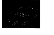
- the image shown in FIG. 20 is displayed on the screen, and in the case of ternary values, the image shown in FIG. 21 is displayed on the screen, and in each case, the pattern predicted by the simulation calculation is displayed.
- the inverted characters “ABC” in the first-order diffraction image could be suppressed.
- Example 3 In Example 3, a two-photon absorption dye was used as a dye, and a diffractive optical element was manufactured using a pulse laser as a light source.
- the polymer two-photon absorption compound B having the following structure was dissolved in methyl ethyl ketone to prepare a coating solution having a solid concentration of 9% by mass.
- the obtained coating solution was spin-coated on a glass slide serving as a support to form a polymer material layer having a thickness of 1 ⁇ m.
- a pulse laser having a wavelength of 405 nm, a pulse width of 2.0 ps, and a repetition rate of 76 MHz was used.
- the pulse intensity was controlled using an electro-optic modulator (EOM) in the optical path.
- EOM electro-optic modulator
- the objective lens an infinite objective lens having a NA of 0.85 (magnification ⁇ 60) was used.
- the pulse laser was set so that the peak power on the surface of the polymer material layer was 60 W, and the number of irradiation pulses was controlled by EOM so that dots with an interval of 300 nm were formed.
Landscapes
- Physics & Mathematics (AREA)
- General Physics & Mathematics (AREA)
- Optics & Photonics (AREA)
- Engineering & Computer Science (AREA)
- Manufacturing & Machinery (AREA)
- Laser Beam Processing (AREA)
Description
本発明は、画像表示デバイスやセキュリティ素子、光学フィルタ素子などとして利用することが可能な回折光学素子ならびに回折光学素子の製造方法および製造装置に関する。
従来、回折光学素子を製造する方法として、フォトレジストに微細露光を行ってマスクを作成し、エッチングにより凹凸を形成する方法が知られている(特許文献1)。また、高分子材料の表面にレーザ光を照射することで、レーザアブレーションにより微細な凹凸形状を形成し、回折光学素子を製造する方法も知られている(特許文献2)。
しかし、特許文献1の方法のようにマスクを作成してエッチングを行うのは、多くの工程を必要とする。一方、特許文献2の方法のように、レーザアブレーションで加工をする場合、エッチングは不要であるが、加工に多くのエネルギが必要であるから、パルスレーザや紫外レーザを用いる必要があり、加工時間も長いという問題がある。また、レーザアブレーションによる加工は、所望のパターンで微細な加工をしたり、より高精度な回折光学素子を実現する多段階の形状に階調制御したパターンを実現するのが困難であるという問題がある。
簡易かつ高速に製造することができる回折光学素子ならびに回折光学素子の製造方法および製造装置を提供することが本発明の諸態様の一つの側面である。
本発明の一態様としての回折光学素子は、高分子材料層を有し、当該高分子材料層は、高分子材料と、高分子材料層中に分散され、または、高分子材料層中の高分子材料に共有結合された色素とを有し、高分子材料層の界面に、ドット状の開口および/または凸部による回折光学素子パターンが配列されてなることを特徴とする。
このような回折光学素子によれば、製造時には、高分子材料層に含まれる色素にレーザ光を吸収させることで、高い効率で高分子材料層にエネルギを与え、高分子材料層の界面に開口および/または凸部を形成して回折光学素子パターンを形成することが可能である。そのため、エッチングが不要な上、短い照射時間で簡単に製造することが可能である。また、レーザアブレーションのように材料を剥離させるのではなく、界面を変形させることで開口および/または凸部を形成するので、微細かつ階調制御が可能な回折光学素子パターンを形成することができる。なお、本発明においていう開口は、底のある凹部であってもよいし高分子材料層を貫通していてもよい。
前記した回折光学素子において、色素は、1光子吸収色素を含むことができる。色素が1光子吸収色素を含むと、半導体レーザなど低エネルギのレーザで加工をすることが可能である。
前記した回折光学素子において、色素は、多光子吸収色素を含んでもよい。多光子吸収色素を含む場合、可視波長域で透過性の高い回折光学素子とすることができる。
前記した回折光学素子は、高分子材料層を支持する支持体を有することができる。支持体を備えることで、高分子材料層を薄くしてコストダウンを図ることができる。
前記した回折光学素子は、高分子材料層の開口および/または凸部が配列された側に、カバー層を備えることが望ましい。開口および/または凸部が配列された側にカバー層を備えると、開口および/または凸部を保護して回折光学素子の機能を保持することができる。
前記した回折光学素子において、開口および/または凸部は、深さまたは高さの異なる複数種類があり、当該複数種類の開口および/または凸部により、多値の回折光学素子パターンが形成されている構成とすることができる。このように多値の回折光学素子パターンを構成することで、不要な回折像の除去をするなど、回折光学素子の機能を高めることができる。そして、開口および/または凸部の、深さまたは高さを異ならせるためには、レーザ光の照射時間を調整すればよいだけであるので、簡単に高機能な回折光学素子を製造することができる。
前記した回折光学素子において、色素は、吸収波長帯域が、主として450nm以下にあり、かつ、450~800nmの波長の光透過率が50%以上であることが望ましい。すなわち、色素が主として450nm以下の波長域の光を吸収することで、比較的無色の(可視波長域で透過性が高い)回折光学素子にすることができる。
本発明の他の態様としての回折光学素子の製造方法は、色素が分散された高分子材料または色素が共有結合された高分子材料を有する高分子材料層を準備し、高分子材料層の界面近傍に色素が吸収する波長のレーザ光を照射して界面を変形させ、この照射を界面において、所定のパターンで行うことで界面に回折光学素子パターンを構成するドット状の開口および/または凸部を形成することを特徴とする。
このような製造方法によれば、高分子材料層に含まれる色素にレーザ光を吸収させることで、高い効率で高分子材料層にエネルギを与えることができる。そのため、エッチングが不要な上、短い照射時間で簡単に回折光学素子を製造することができる。また、レーザ光を界面に走査させることで界面に回折光学素子パターンを形成するので、従来のようにマスクを用いる必要が無くなる。さらに、レーザアブレーションのように材料を剥離させるのではなく、界面を変形させることで開口および/または凸部を形成するので、微細かつ階調制御が可能な光学素子パターンを形成することができる。
前記した方法において、1つの開口または凸部を形成するためのレーザ光の照射時間は、120μsec以下であることが望ましい。照射時間を短くすることで、高速に回折光学素子を製造することができる。
前記した方法においては、レーザ光の照射中に、界面からの反射光をセンサにより検出し、当該センサの出力信号に基づいてレーザ光の焦点位置を所定位置に調整することが望ましい。このように、界面からの反射光に基づいて焦点位置を調整することで、開口または凹部の大きさを揃えて、所望の性能の回折光学素子を得ることができる。
本発明のさらに他の態様としての回折光学素子の製造装置は、色素が分散された高分子材料または色素が共有結合された高分子材料を有する高分子材料層に回折光学素子パターンを形成するための回折光学素子の製造装置であって、色素が吸収する波長のレーザ光を発する光源と、光源から出射されたレーザ光を偏向させる偏向器と、偏向器で偏向されたレーザ光を高分子材料層の界面近傍に結像させるための結像光学系と、光源の出力および偏向器を制御する制御装置とを備え、制御装置は、高分子材料層の界面に回折光学素子パターンを構成するドット状の開口および/または凸部を形成するように、偏向器を制御して高分子材料層の界面にレーザ光を走査するのに同期させて、光源の出力を変化させるように構成されたことを特徴とする。
このような製造装置によれば、偏向器によりレーザ光を走査させつつ光源の出力を変化させ、高分子材料層の界面に開口および/または凸部を形成して光学回折素子を製造することができる。また、レーザ光を界面に走査させることで界面に回折光学素子パターンを形成するので、従来のようにマスクを用いる必要が無くなる。さらに、この製造装置では、偏向器でレーザ光を界面上に走査させることで、回折光学素子パターンを形成するので、高分子材料層を加工中に移動させる必要がない。そして、この製造装置は、色素を含む高分子材料層にレーザ光を照射して開口および/または凸部を形成するので、レーザ光の出力を小さくでき、また、高速で加工をすることができる。
前記した製造装置において、結像光学系は、対物レンズと、少なくとも2枚の集光レンズとを含むことが望ましい。このような、対物レンズと2枚の集光レンズとを含む光学系にすることで、シンプルな構成で縮小された微細な光学回折素子パターンを形成することができる。
前記した製造装置においては、1つの開口または凸部を形成するためのレーザ光の照射時間が120μsec以下であることが望ましい。照射時間を短くすることで、高速に回折光学素子を製造することができる。
前記した製造装置において、結像光学系は、対物レンズを含み、対物レンズは、開口数が0.13以上であることが望ましい。これにより、レーザ光を小さく集光して、開口および/または凸部を形成することができる。
前記した製造装置は、界面で反射したレーザ光を検出するセンサをさらに備え、制御装置は、センサの出力信号に基づいて結像光学系を制御してレーザ光の焦点位置を所定位置に調整するように構成されることが望ましい。
このように、界面で反射したレーザ光に基づいて焦点位置を調整することで、開口または凹部の大きさを揃えて、所望の性能の回折光学素子を得ることができる。
前記した製造装置において、光源が発するレーザ光の波長は450nm以下であることが望ましい。このような波長のレーザを用いることで、色素として、可視光をあまり吸収しないものを用いることができるので、回折光学素子を比較的無色にすることができる。
前記した製造装置においては、高分子材料層を、レーザ光に対して移動させる搬送装置を有することが望ましい。搬送装置により高分子材料層を移動させることで、複数の回折光学素子を連続的に製造することが可能となる。
上述のような態様の回折光学素子ならびにその製造方法および製造装置によれば、回折光学素子を短い時間で簡単に製造することができる。回折光学素子の製造方法および製造装置によれば、レーザ光を界面に走査させることで界面に回折光学素子パターンを形成するので、従来のようにマスクを用いる必要が無くなる。さらに、回折光学素子の製造装置によれば、偏向器でレーザ光を界面上に走査させることで、回折光学素子パターンを形成するので、高分子材料層を加工中に移動させる必要がない。
次に、本発明の実施形態について、図面を参照しながら説明する。
図1に示すように本発明の回折光学素子Eは、シート状の部材の所定範囲に微細なドット状の開口および/または凸部を形成することで回折光学素子パターンを形成したものである。図1において、回折光学素子パターンが形成されたパターン領域PAは、一例として正方形を有しているが、パターン領域PAの形状は特に限定されない。もっとも、少ない材料(後述する高分子材料層)から多くの回折光学素子Eを得る観点からは、パターン領域PAを正方形として、隣接する回折光学素子と所定の隙間を開けて形成するのが、効率的である。
図1に示すように本発明の回折光学素子Eは、シート状の部材の所定範囲に微細なドット状の開口および/または凸部を形成することで回折光学素子パターンを形成したものである。図1において、回折光学素子パターンが形成されたパターン領域PAは、一例として正方形を有しているが、パターン領域PAの形状は特に限定されない。もっとも、少ない材料(後述する高分子材料層)から多くの回折光学素子Eを得る観点からは、パターン領域PAを正方形として、隣接する回折光学素子と所定の隙間を開けて形成するのが、効率的である。
本実施形態においては、回折光学素子Eとして、レーザ光を当てることにより、所定の画像となる回折像を得るものを例示する。この回折光学素子Eは、例えば、図2に示すように、再生用レーザL2、回折光学素子E、スクリーンSCの順に配置して、再生用レーザL2から再生用レーザ光LB2を出射し、この再生用レーザ光LB2をパターン領域PAに通過させて回折光DBを得るように使用する。このように、パターン領域PAに再生用レーザ光LB2を照射することで、回折光DBが所定の画像を表示するようになっている。
また、回折光学素子Eは、図3に示すように使用することもできる。すなわち、再生用レーザL2、スクリーンSC、回折光学素子Eの順に配置し、スクリーンSCに孔SC1を形成しておく。そして、再生用レーザL2から出射した再生用レーザ光LB2をこの孔SC1を通して回折光学素子Eのパターン領域PAに当てる。このようにすることで、再生用レーザ光LB2は回折光学素子Eの回折光学素子パターンが形成された界面で反射されつつ、その回折光学素子パターンで回折され、スクリーンSCに所定の画像を表示することができる。
また、回折光学素子Eは、図3に示すように使用することもできる。すなわち、再生用レーザL2、スクリーンSC、回折光学素子Eの順に配置し、スクリーンSCに孔SC1を形成しておく。そして、再生用レーザL2から出射した再生用レーザ光LB2をこの孔SC1を通して回折光学素子Eのパターン領域PAに当てる。このようにすることで、再生用レーザ光LB2は回折光学素子Eの回折光学素子パターンが形成された界面で反射されつつ、その回折光学素子パターンで回折され、スクリーンSCに所定の画像を表示することができる。
次に、本発明の回折光学素子Eの様々な実施形態について、それぞれ断面図を参照して説明する。
[第1実施形態]
図4に示すように、第1実施形態に係る回折光学素子Eは、支持体10の上に、高分子材料層20が設けられた2層からなる構造を有する。
図4に示すように、第1実施形態に係る回折光学素子Eは、支持体10の上に、高分子材料層20が設けられた2層からなる構造を有する。
支持体10は、高分子材料層20を支持するための部材である。
支持体10の材料は、特に限定されないが、再生用レーザ光LB2を透過させて使用するため、一例として、再生用レーザL2の再生用レーザ光LB2が透過可能な材料からなる。もっとも、支持体10は、再生用レーザ光LB2に対し不透明な部材であってもよい。例えば、支持体10を金属板にして、支持体10の高分子材料層20側の面を反射面として利用してもよい。
支持体10の厚さは、高分子材料層20を支持するのに十分な力学的性質を有すれば特に制限はなく、例えば、1mm以下程度のフィルムであってもよいし、1mm以上程度の板状の部材であってもよい。
支持体10の材料は、特に限定されないが、再生用レーザ光LB2を透過させて使用するため、一例として、再生用レーザL2の再生用レーザ光LB2が透過可能な材料からなる。もっとも、支持体10は、再生用レーザ光LB2に対し不透明な部材であってもよい。例えば、支持体10を金属板にして、支持体10の高分子材料層20側の面を反射面として利用してもよい。
支持体10の厚さは、高分子材料層20を支持するのに十分な力学的性質を有すれば特に制限はなく、例えば、1mm以下程度のフィルムであってもよいし、1mm以上程度の板状の部材であってもよい。
高分子材料層20は、界面、ここでは、空気層との界面21にドット状の開口および/または凸部(以下、これを「格子点」と呼ぶことがある。)による回折光学素子パターンが形成される層である。図4の例では、開口の一例として凹部31が複数形成されている。図4の凹部31は、平面的に見たときにドット状であり、いずれも深さおよび直径が略同じである。回折光学素子パターンは、所望の再生画像に応じて設計され、例えば、図16、図17のレーザ顕微鏡像のようなパターンとなっている。
高分子材料層20は、分散された色素または高分子材料層20中の高分子材料に共有結合された色素を有している。色素が高分子材料に共有結合されている場合、長期間の保存による色素の析出や溶出を防止し、透過率、反射率などの光学的特性の経時変化を小さくでき、長期保存性に優れた回折光学素子を構成することができる。
ここでの色素は、1光子吸収色素および/または多光子吸収色素を含むことができる。1光子吸収色素を含む場合、半導体レーザなど低エネルギのレーザで加工をすることが可能である。一方、多光子吸収色素を含む場合、可視波長域で透過性の高い回折光学素子E1を構成することができる。1光子吸収色素は、再生用レーザ光LB2の波長に線形吸収帯を持たない1光子吸収化合物であることが好ましく、多光子吸収色素は、再生用レーザ光LB2の波長に線形吸収帯を持たない多光子吸収化合物であることが好ましい。
高分子材料層20の、格子点を形成するためのレーザ光(記録用レーザ光)に対する吸収率(一光子吸収率)は、厚み1μm当たり5%以上であるのが望ましく、10%以上であるのがより望ましい。吸収率が大きいほど、記録用レーザ光の照射時に迅速に高分子材料を昇温することができ、短い時間で回折光学素子E1を形成することができ、また、低エネルギのレーザ光源を使用することができる。
高分子材料層20の形成方法は、特に限定されないが、色素材料と高分子材料を溶媒に溶解させた液を用いてスピンコートやブレードコートなどにより形成することができる。このときの溶媒としては、ジクロロメタン、クロロホルム、メチルエチルケトン(MEK)、アセトン、メチルイソブチルケトン(MIBK)、トルエン、ヘキサンなどを用いることができる。
高分子材料層20に用いる高分子材料としては、ポリ酢酸ビニル(PVAc)、ポリメチルメタクリレート(PMMA)、ポリエチルメタクリレート、ポリブチルメタクリレート、ポリベンジルメタクリレート、ポリイソブチルメタクリレート、ポリシクロヘキシルメタクリレート、ポリカーボネート(PC)、ポリスチレン(PS)、ポリ塩化ビニル(PVC)、ポリビニルアルコール(PVA)などを用いることができる。
高分子材料層20中の高分子材料(または色素が共有結合された高分子材料)の分子量Mwの範囲は、10,000~1,000,000が好ましい。分子量が10,000より低いと、高分子材料自身の流動性が高くなり支持体やカバー層などの隣接層への染み出し(拡散)が生じ、保存安定性に問題を生じる可能性がある。また、分子量が1,000,000より高いと、高分子材料層の塗布形成時に、粘度が高くなりすぎて均一な成膜が困難になる可能性がある。なお、分子量Mwは、ゲル浸透クロマトグラフィー(GPC)により測定可能である。
高分子材料のガラス転移点Tgは60℃以上であることが好ましく、100℃以上であることがより好ましい。ガラス転移点Tgが高いことで、熱的な安定性を向上させ、特に加工後の界面の形状変化が抑制され、長期間、安定して回折光学素子の特性を維持することができる。また、高分子材料のガラス転移点Tgは、高速な格子点の加工を実現するために300℃以下であることが好ましい。
高分子材料層20中の高分子材料(または色素が共有結合された高分子材料)の分子量Mwの範囲は、10,000~1,000,000が好ましい。分子量が10,000より低いと、高分子材料自身の流動性が高くなり支持体やカバー層などの隣接層への染み出し(拡散)が生じ、保存安定性に問題を生じる可能性がある。また、分子量が1,000,000より高いと、高分子材料層の塗布形成時に、粘度が高くなりすぎて均一な成膜が困難になる可能性がある。なお、分子量Mwは、ゲル浸透クロマトグラフィー(GPC)により測定可能である。
高分子材料のガラス転移点Tgは60℃以上であることが好ましく、100℃以上であることがより好ましい。ガラス転移点Tgが高いことで、熱的な安定性を向上させ、特に加工後の界面の形状変化が抑制され、長期間、安定して回折光学素子の特性を維持することができる。また、高分子材料のガラス転移点Tgは、高速な格子点の加工を実現するために300℃以下であることが好ましい。
また、高分子材料に分散される色素または高分子材料に共有結合される色素としては、1光子吸収色素であれば、メチン色素(シアニン色素、ヘミシアニン色素、スチリル色素、オキソノール色素、メロシアニン色素など)、大環状色素(フタロシアニン色素、ナフタロシアニン色素、ポルフィリン色素など)、アゾ色素(アゾ金属キレート色素含む)、アリリデン色素、錯体色素、クマリン色素、アゾール誘導体、トリアジン誘導体、ベンゾトリアゾール誘導体、ベンゾフェノン誘導体、フェノキサジン誘導体、フェノチアジン誘導体、1-アミノブタジエン誘導体、桂皮酸誘導体、キノフタロン系色素などを使用することができる。このうち、トリアジン誘導体、ベンゾトリアゾール誘導体、ベンゾフェノン誘導体は、紫外線吸収色素であり、吸収波長帯域が主として450nm以下にあり、かつ、450~800nmの波長の光透過率が50%以上である。そのため、これらの色素を使用した場合、主として450nm以下の波長域の光を吸収するので、比較的無色の回折光学素子E1を構成することができる。
また、多光子吸収色素を用いる場合、色素化合物は、再生用レーザ光LB2の波長に線形吸収帯を持たないものであれば、特に限定されないが、例えば、下記一般式(1)で表される構造を有する化合物が挙げられる。

(一般式(1)中、XおよびYはハメットのシグマパラ値(σp値)が共にゼロ以上の値を有する置換基を表し、同一でもそれぞれ異なってもよく、nは1~4の整数を表し、Rは置換基を表し、同一でもそれぞれ異なってもよく、mは0~4の整数を表す。)
一般式(1)中、XおよびYはハメット式におけるσp値が正の値を取るもの、所謂電子吸引性の基を指し、好ましくは例えばトリフルオロメチル基、ヘテロ環基、ハロゲン原子、シアノ基、ニトロ基、アルキルスルホニル基、アリールスルホニル基、スルファモイル基、カルバモイル基、アシル基、アシルオキシ基、アルコキシカルボニル基、などが挙げられ、より好ましくはトリフルオロメチル基、シアノ基、アシル基、アシルオキシ基、またはアルコキシカルボニル基であり、最も好ましくはシアノ基、ベンゾイル基である。これらの置換基のうち、アルキルスルホニル基、アリールスルホニル基、スルファモイル基、カルバモイル基、アシル基、アシルオキシ基、およびアルコキシカルボニル基は、溶媒への溶解性の付与等の他、様々な目的で、更に置換基を有してもよく、置換基としては、好ましくは、アルキル基、アルコキシ基、アルコキシアルキル基、アリールオキシ基、などが挙げられる。
nは好ましくは2または3であり、最も好ましくは2である。nが5以上になるほど、線形吸収が長波長側に出てくるようになり、700nmよりも短波長の領域の記録光を用いての非共鳴2光子吸収記録ができなくなる。
Rは置換基を表し、置換基としては、特に限定されず、具体的には、アルキル基、アルコキシ基、アルコキシアルキル基、アリールオキシ基、などが挙げられる。
Rは置換基を表し、置換基としては、特に限定されず、具体的には、アルキル基、アルコキシ基、アルコキシアルキル基、アリールオキシ基、などが挙げられる。
一般式(1)で表される構造を有する化合物の具体例としては、特に限定されないが、下記の化学構造式D-1~D-21の化合物を使用することができる。
また、色素が共有結合された高分子材料としては、例えば、下記の一般式(2)で示す化合物を使用することができる。

(一般式(2)中、Yはハメットのシグマパラ値(σp値)が共にゼロ以上の値を有する置換基を表し、Xも同種の置換基を表す。XおよびYは同一種でもそれぞれ異なってもよく、nは1~4の整数を表し、R1、R2、R3は置換基を表し、同一種でもそれぞれ異なってもよく、lは1以上、mは0~4の整数を表す。)
以上の構成による回折光学素子E1によれば、高分子材料層20に記録用レーザ光を集光して照射することで凹部31を形成し、回折光学素子E1を製造することができる。このとき、高分子材料層20に含まれる色素に記録用レーザ光を吸収させることで高い効率で高分子材料層20にエネルギを与え、短い時間で回折光学素子E1を製造することができる。また、回折光学素子E1は、製造時にエッチングが不要であることからも短い時間で製造することができる。また、レーザアブレーションのように材料を剥離させるのではなく、界面を変形させることで凹部31を形成するので、微細かつ階調制御可能な光学素子パターンを形成することができる。さらに、支持体10に高分子材料層20を支持させることで高分子材料層20を薄くすることができ、コストダウンを図ることができる。
[第2実施形態]
次に、回折光学素子Eの第2実施形態について説明する。なお、以下の各実施形態において、高分子材料層20および支持体10は、第1実施形態と同様の構成を採用することができる。
図5に示すように、第2実施形態の回折光学素子E2は、支持体10と、高分子材料層20を有するとともに、高分子材料層20の支持体10とは反対側の格子点が配列された側に、カバー層41を備えている。カバー層41は、格子点の形状を、力学的または化学的に保護するためのものである。カバー層41の構成は、格子点に悪影響が無ければ特に限定されず、例えば、紫外線硬化樹脂を塗布して硬化させることで設けることができる。また、図示は省略するが、粘着剤のついたフィルム(ポリカーボネートなど)を貼り付けてカバー層41を構成してもよい。
次に、回折光学素子Eの第2実施形態について説明する。なお、以下の各実施形態において、高分子材料層20および支持体10は、第1実施形態と同様の構成を採用することができる。
図5に示すように、第2実施形態の回折光学素子E2は、支持体10と、高分子材料層20を有するとともに、高分子材料層20の支持体10とは反対側の格子点が配列された側に、カバー層41を備えている。カバー層41は、格子点の形状を、力学的または化学的に保護するためのものである。カバー層41の構成は、格子点に悪影響が無ければ特に限定されず、例えば、紫外線硬化樹脂を塗布して硬化させることで設けることができる。また、図示は省略するが、粘着剤のついたフィルム(ポリカーボネートなど)を貼り付けてカバー層41を構成してもよい。
また、第2実施形態の回折光学素子E2は、第1実施形態と異なり、格子点が凸部32により構成されている。格子点を開口にするか凸部にするかは、記録用レーザ光を照射したときの高分子材料層20の吸収エネルギ(出力、照射時間および吸収率)によって決まり、吸収エネルギが小さいと凸部になりやすく、大きいと開口になりやすい。
以上の構成による回折光学素子E2によれば、カバー層41により、格子点を保護し、長期保存も可能である。なお、格子点は、カバー層41を設けた後に形成するのが望ましい。こうすることにより、カバー層41を設ける際に格子点の形状が乱れることがなく、また、カバー層41と高分子材料層20の間に空気などが介在することを抑制することができる。
[第3実施形態]
図6に示すように、第3実施形態に係る回折光学素子E3は、第1実施形態に対し、格子点が、高分子材料層20を貫通した穴33とした形態である。このような穴33は、高分子材料層20を薄く形成し、格子点の形成の際に大きなエネルギで高分子材料層20を露光すればよい。このような穴33を格子点としても、第1実施形態と同様に、回折光学素子の機能を発揮することができ、また、簡単かつ短い時間で製造することができる。
図6に示すように、第3実施形態に係る回折光学素子E3は、第1実施形態に対し、格子点が、高分子材料層20を貫通した穴33とした形態である。このような穴33は、高分子材料層20を薄く形成し、格子点の形成の際に大きなエネルギで高分子材料層20を露光すればよい。このような穴33を格子点としても、第1実施形態と同様に、回折光学素子の機能を発揮することができ、また、簡単かつ短い時間で製造することができる。
なお、このような高分子材料層20を貫通した穴33を形成した形態においては、高分子材料層20の色素が可視波長域の光を多く(例えば、50%以上)吸収するようにすれば、再生時において、穴33に再生用レーザ光LB2を通過させ、穴33を通過した光の回折光を利用することができる。
[第4実施形態]
図7に示すように、第4実施形態に係る回折光学素子E4は、第1実施形態に対し、支持体10を無くしたもので、支持体10を備える代わりに高分子材料層20の厚さを厚くして、回折光学素子E4の形状を維持するように構成したものである。高分子材料層20は、1mm以下程度のフィルムであってもよいし、1mm以上程度の板状の部材であってもよい。
図7に示すように、第4実施形態に係る回折光学素子E4は、第1実施形態に対し、支持体10を無くしたもので、支持体10を備える代わりに高分子材料層20の厚さを厚くして、回折光学素子E4の形状を維持するように構成したものである。高分子材料層20は、1mm以下程度のフィルムであってもよいし、1mm以上程度の板状の部材であってもよい。
このような構成の回折光学素子E4によれば、支持体を省略することで、製造工程を簡略化することができる。
[第5実施形態]
図8に示すように、第5実施形態に係る回折光学素子E5は、第1実施形態に対し、高分子材料層20の空気との界面ではなく、支持体側の内側の界面に格子点としての凹部31を形成したものである。この形態においては、内側の界面が変形しやすいように、支持体10と高分子材料層20の間に、高分子材料層20よりも軟らかい(例えば、ガラス転移点Tgが低い)層である粘着層42が介在されている。このように、高分子材料層20の内側の界面に格子点を形成する場合、記録用レーザ光を、この内側の界面付近に集光して照射すればよい。なお、当然のことであるが、格子点は、高分子材料層20を基準に見て凸部となっていてもよい(高分子材料層20から突出していてもよい)。
図8に示すように、第5実施形態に係る回折光学素子E5は、第1実施形態に対し、高分子材料層20の空気との界面ではなく、支持体側の内側の界面に格子点としての凹部31を形成したものである。この形態においては、内側の界面が変形しやすいように、支持体10と高分子材料層20の間に、高分子材料層20よりも軟らかい(例えば、ガラス転移点Tgが低い)層である粘着層42が介在されている。このように、高分子材料層20の内側の界面に格子点を形成する場合、記録用レーザ光を、この内側の界面付近に集光して照射すればよい。なお、当然のことであるが、格子点は、高分子材料層20を基準に見て凸部となっていてもよい(高分子材料層20から突出していてもよい)。
このような構成の回折光学素子E5によれば、支持体10がカバー層として機能して格子点が最外表面に露出しないので、別途、カバー層41を設けなくても、格子点の形状を保護することができる。
[第6実施形態]
図9に示すように、第6実施形態に係る回折光学素子E6は、第1実施形態に対し、高分子材料層20の外側の表面に、反射層43を設けたものである。反射層43は、金属の薄膜であってもよいし、高分子材料層20に比較して屈折率が大きく異なる材料からなる層であってもよい。このような構成の回折光学素子E6によると、図9に矢印で示したように、再生用レーザ光LB2を反射層43で反射させ、回折光学素子E6に対し再生用レーザ光LB2が入射する側に再生画像を形成することができる。なお、図9では、反射層43の外側(図の上側)から再生用レーザ光LB2を照射するように示したが、反対側(図の下側)から再生用レーザ光LB2を照射しても構わない。
図9に示すように、第6実施形態に係る回折光学素子E6は、第1実施形態に対し、高分子材料層20の外側の表面に、反射層43を設けたものである。反射層43は、金属の薄膜であってもよいし、高分子材料層20に比較して屈折率が大きく異なる材料からなる層であってもよい。このような構成の回折光学素子E6によると、図9に矢印で示したように、再生用レーザ光LB2を反射層43で反射させ、回折光学素子E6に対し再生用レーザ光LB2が入射する側に再生画像を形成することができる。なお、図9では、反射層43の外側(図の上側)から再生用レーザ光LB2を照射するように示したが、反対側(図の下側)から再生用レーザ光LB2を照射しても構わない。
[第7実施形態]
図10に示すように、第7実施形態に係る回折光学素子E7は、第1実施形態に対し、格子点を、一定深さの凹部31だけでなく、異なる深さ、例えば、凹部31よりも深い凹部31Bを混在させて配置したものである。凹部の深さを異ならせるには、製造時に、記録用レーザ光の照射時間を異ならせればよい。記録用レーザ光を短い時間照射すれば浅い凹部となり、長い時間照射すれば深い凹部となる。
図10に示すように、第7実施形態に係る回折光学素子E7は、第1実施形態に対し、格子点を、一定深さの凹部31だけでなく、異なる深さ、例えば、凹部31よりも深い凹部31Bを混在させて配置したものである。凹部の深さを異ならせるには、製造時に、記録用レーザ光の照射時間を異ならせればよい。記録用レーザ光を短い時間照射すれば浅い凹部となり、長い時間照射すれば深い凹部となる。
このように、深さが異なる凹部31、凹部31Bがあると、使用時に再生用レーザ光LB2が各格子点で回折したときに、格子点ごとに回折した光の光路長に違いがでることから、複数の格子点により回折した再生用レーザ光LB2が干渉することで決定される進行方向である回折角を調整することができる。このため、凹部31、凹部31Bを用いた多値化された回折格子により、反転画像や、2次の回折像を淡くするなど、画像にバリエーションを持たせることができる。
なお、ここでは、格子点に、2種類の深さの凹部31、凹部31Bを混在させる場合を例示したが、3種類以上の深さの凹部を混在させてもよい。
なお、ここでは、格子点に、2種類の深さの凹部31、凹部31Bを混在させる場合を例示したが、3種類以上の深さの凹部を混在させてもよい。
[第8実施形態]
図11に示すように、第8実施形態に係る回折光学素子E8は、第1実施形態に対し、格子点を、凹部31だけではなく、凸部32を混在させて配置したものである。
このように、凹部31と凸部32があると、第7実施形態と同様に、使用時に再生用レーザ光LB2が各格子点で回折したときに、格子点ごとに回折した光の光路長に違いがでることから、複数の格子点により回折した再生用レーザ光LB2が干渉することで決定される進行方向である回折角を調整することができる。このため、凹部31、凸部32を用いた多値化された回折格子により、反転画像や、2次の回折像を淡くするなど、画像にバリエーションを持たせることができる。
図11に示すように、第8実施形態に係る回折光学素子E8は、第1実施形態に対し、格子点を、凹部31だけではなく、凸部32を混在させて配置したものである。
このように、凹部31と凸部32があると、第7実施形態と同様に、使用時に再生用レーザ光LB2が各格子点で回折したときに、格子点ごとに回折した光の光路長に違いがでることから、複数の格子点により回折した再生用レーザ光LB2が干渉することで決定される進行方向である回折角を調整することができる。このため、凹部31、凸部32を用いた多値化された回折格子により、反転画像や、2次の回折像を淡くするなど、画像にバリエーションを持たせることができる。
なお、ここでは、格子点に、凹部31、凸部32を混在させる場合を例示したが、凹部31の深さや、凸部32の高さを異ならせたものをさらに混在させて、さらに多値化された回折格子を構成してもよい。
第7、第8実施形態の説明から分かるように、格子点を構成する開口および/または凸部は、深さまたは高さの異なる複数種類があり、当該複数種類の格子点により、多値の回折光学素子パターンが形成されている構成とすることができる。そして、開口および/または凸部の、深さまたは高さを異ならせるためには、記録用レーザ光の照射時間を調整すればよいだけであるので、簡単に高機能な回折光学素子を製造することができる。
以上に、様々な形態の回折光学素子Eを例示したが、上記の各回折光学素子Eの特徴は、互いに組み合わせて適用することが可能である。
[回折光学素子の製造装置]
次に、回折光学素子Eの製造装置について説明する。
図12に示すように、製造装置50は、光源である記録用レーザ51と、偏向器52と、ステージ57と、結像光学系60と、制御装置59とを主に備えている。
次に、回折光学素子Eの製造装置について説明する。
図12に示すように、製造装置50は、光源である記録用レーザ51と、偏向器52と、ステージ57と、結像光学系60と、制御装置59とを主に備えている。
記録用レーザ51は、記録用レーザ光LB1を出射するレーザであり、半導体レーザであることが望ましい。記録用レーザ光LB1の波長は、高分子材料層20中の色素が吸収する(1光子吸収および/または多光子吸収)波長であり、回折光学素子Eの使用時に使用する再生用レーザ光LB2の波長と異なることが望ましい。これにより、再生時に回折光学素子Eが再生用レーザ光LB2により加熱されることが抑制されるので、再生時に大きな出力の再生用レーザ光LB2を使用することができる。
特に画像表示の用途の回折光学素子Eを製造する場合には、回折光学素子Eの可視波長域での透明性が高いことが望ましく、そのため、記録用レーザ51としては、450nm以下の波長の記録用レーザ光LB1を発するものであることが望ましい。
特に画像表示の用途の回折光学素子Eを製造する場合には、回折光学素子Eの可視波長域での透明性が高いことが望ましく、そのため、記録用レーザ51としては、450nm以下の波長の記録用レーザ光LB1を発するものであることが望ましい。
微細な回折パターン(再生画像)を描画するためには、記録用レーザ51は、記録用レーザ光LB1のスポットサイズを小さくすることが可能な短波長レーザであることが望ましく、特に、400~410nmの半導体レーザであるとよい。
高分子材料層20中の色素として多光子吸収色素を用いる場合には、記録用レーザ51は、ピークパワーが大きい短パルスレーザを用いることが望ましい。そして、色素に吸収されるエネルギが大きいことが望ましく、ピークパワーとパルス幅と繰り返し周期の積である平均パワーが大きいパルスレーザがよい。例えば、記録用レーザ51は、平均パワーが、10mW以上、より好ましくは100mW以上の出力を有しているとよい。なお、高分子材料層20中の色素として多光子吸収色素を用いる場合には、線形吸収の無い波長を用いるため、特に可視波長域における透明性が高い回折光学素子Eを作りやすい。
偏向器52は、記録用レーザ51から出射された記録用レーザ光の進行方向を偏向する器械であり、ガルバノミラーや、ポリゴンミラー、レゾナントミラーなどを使用することができる。もしくは、偏向器52は、電気光学素子(EO素子)を採用して、記録用レーザ光LB1の進行方向を偏向させてもよい。
偏向器52は、少なくとも1方向について記録用レーザ光LB1を偏向すればよい。もっとも、2軸のガルバノミラーなど、2方向に偏向させる偏向器を用いる場合には、ステージ57に載置される回折光学素子Eの素材EM(格子点が未記録のもの)を動かさなくても、回折光学素子パターンを製造することができる。なお、1方向についてのみ偏向する偏向器52を用いる場合には、その1方向に直交する方向に、素材EMを搬送できるようにステージ57を構成するとよい。
ステージ57は、素材EMが載置される台である。ステージ57は、素材EMを固定したまま移動させないものであってもよいが、図13に示すように、一方向に素材EMを搬送できるように構成されている搬送ステージであることが望ましい。例えば、搬送ステージ570は、帯状の素材EMを巻き取る巻取ローラ571と巻き出す巻出ローラ572とを有し、巻取ローラ571と巻出ローラ572の間で素材EMを張りながら搬送するものである。このような搬送ステージ570を採用することで、素材EMを搬送するとともに、偏向器52で、少なくとも搬送ステージ570の搬送方向に交差する方向(例えば、直交する方向)に記録用レーザ光LB1を走査することで、連続的に回折光学素子Eを製造することができる。なお、このとき、偏向器52は、搬送ステージ570の搬送方向に交差する方向にのみ記録用レーザ光LB1を偏向するのでもよいし、搬送ステージ570の搬送方向に交差する方向と、搬送方向の両方の方向に偏向するのでもよい。後者の場合、一列の回折光学素子Eを製造する間は、搬送ステージ570を停止させておき、一列の回折光学素子Eを製造する度に搬送ステージ570を作動させて素材EMを1列分搬送するとよい。
図12に示すように、結像光学系60は、第1集光レンズ61と、第2集光レンズ62と、対物レンズ63を有して構成されている。第1集光レンズ61と第2集光レンズ62は、ともに同じ焦点距離fを持つレンズであり、これらにより、いわゆる4f光学系を構成している。偏向器52の反射面は、第1集光レンズ61の前側の焦点位置近傍に配置されている。対物レンズ63は、第2集光レンズ62を通過した記録用レーザ光LB1を高分子材料層20の界面近傍に結像させる集光レンズであり、第2集光レンズ62の焦点位置に配置されている。対物レンズ63には、フォーカスアクチュエータ63Aが設けられている。対物レンズ63は、走査範囲において、偏向角に対して像高が比例関係になるように補正されるfθレンズであることが望ましい。また、対物レンズ63は、開口数が0.13以上であることが望ましい。これにより、記録用レーザ光LB1を小さく集光して、微細な格子点を形成することができる。
図14に示すように、4f光学系を採用することで、偏向器52により偏向された所定のビーム径を有する記録用レーザ光LB1は、第1集光レンズ61を通過して、偏向されていない記録用レーザ光LB1の進行方向と平行になり、第1集光レンズ61と第2集光レンズ62の中間点で一度、結像する。そして、第2集光レンズ62を通過した後、第2集光レンズ62の後側の焦点位置において、偏向器52を出たときと同じビーム径で、同じ偏向角となる。さらに、この後側の焦点位置にある対物レンズ63により、記録用レーザ光LB1は絞られて、像面IMにおいて微小なスポット状に結像するようになっている。このような結像光学系60により、簡易な構成で、偏向器52で偏向した記録用レーザ光LB1を、高分子材料層20の界面に沿って走査することができる。
図14においては、最も簡易な構成となる4f光学系を例示したが、例えば、偏向器52の2軸の反射ミラー間を4f光学系で構成することで、レーザ走査範囲で集光スポットの収差をより低減させたり、非球面レンズを採用するなどして、結像光学系60を小さく構成することも可能である。
図12に戻り、記録用レーザ51と偏向器52の間にはPBS(偏光ビームスプリッタ)54と、1/4波長板55がこの順に配置されている。また、PBS54の側方にはフォーカス用の受光素子53(センサ)が配置されている。
PBS54は、特定の偏光の光を反射して分離する光学素子であり、記録用レーザ51から出射された記録用レーザ光LB1を通過させて1/4波長板55へ向けて進めるとともに、1/4波長板55から返ってきた光を反射して受光素子53へ向けて進める機能を果たす。
PBS54は、特定の偏光の光を反射して分離する光学素子であり、記録用レーザ51から出射された記録用レーザ光LB1を通過させて1/4波長板55へ向けて進めるとともに、1/4波長板55から返ってきた光を反射して受光素子53へ向けて進める機能を果たす。
1/4波長板55は、直線偏光を円偏光に変換し、円偏光を回転方向に応じた向きの直線偏光に変換する光学素子であり、記録用レーザ光LB1が偏向器52に向かって進むときと、素材EMで反射した後、偏向器52から返ってくるときとで偏光の向きを90°異ならせる役割を果たす。
制御装置59は、受光素子53からの信号を受信して、フォーカスアクチュエータ63Aを制御し、素材EMにおける高分子材料層20の界面付近に記録用レーザ光LB1の焦点を調整する機能を果たす。このフォーカスの調整は、反射光の強度が最大になるように、対物レンズ63と高分子材料層20の相対的な距離を調整したり、記録用レーザ光LB1の走査によって得られる1次元もしくは2次元の光強度プロファイルのコントラストを最大化したり、また、いわゆる非点収差法などを用いたりすることができる。また、制御装置59は、偏向器52を作動させて記録用レーザ光LB1を高分子材料層20に沿って走査させるとともに、予め記憶してある露光データに基づいて記録用レーザ51の出力を制御して記録用レーザ光LB1の出力を変調させる。なお、記録用レーザ51としてパルスレーザを採用する場合には、メカニカルシャッターを制御して記録用レーザ光LB1を遮断するか、好ましくは、高速に変調を行うため電気光学変調素子(EOM)を制御して記録用レーザ光LB1を偏向させることで変調するとよい。
偏向器52の動作とこれらの変調とは、タイミングを同期させることが望ましい。この同期は、例えば、偏向器52で偏向された記録用レーザ光LB1の一部を図示しないセンサで検出して行うことができる。
そして、高分子材料層20の界面の格子点を形成すべき箇所ごとに、記録用レーザ光LB1の照射時間と照射強度の一方または双方を制御することで、格子点の大きさと、開口の深さまたは凸部の高さを調整することができる。
そして、高分子材料層20の界面の格子点を形成すべき箇所ごとに、記録用レーザ光LB1の照射時間と照射強度の一方または双方を制御することで、格子点の大きさと、開口の深さまたは凸部の高さを調整することができる。
なお、1つの格子点を形成するためのレーザ光の照射時間は、120μsec以下であることが望ましい。120μsec以下程度に照射時間を短くすることで、高速に回折光学素子を製造することができる。例えば、格子点が25万個の回折光学素子Eを1分程度で製造することができる。
以上のような製造装置50を用いた回折光学素子Eの製造方法について説明する。
まず、ステージ57に格子点を記録する前の素材EMを載置する。そして、偏向器52を作動させるとともに、偏向器52の動作に同期させて、予め記憶してある露光データに基づいて記録用レーザ51の出力を変調させる。記録用レーザ光LB1は、記録用レーザ51から、PBS54、1/4波長板55を通過して偏向器52に進み、偏向器52で偏向されて結像光学系60に入る。結像光学系60では、偏向された記録用レーザ光LB1は、第1集光レンズ61、第2集光レンズ62および対物レンズ63を通過し、素材EMの高分子材料層20の界面近傍で微細なドット状に結像される。このとき、高分子材料層20において、偏向角に応じた位置に焦点が結像される。この際、高分子材料層20の界面で反射した一部のレーザ光は、結像光学系60、偏向器52および1/4波長板55の順に戻り、偏光の向きが行きに対し90°回転され、PBS54で反射して受光素子53に入る。制御装置59は、受光素子53で受光した信号に基づいてフォーカスアクチュエータ63Aを制御することで記録用レーザ光LB1の焦点が所定の位置になるように調整する。
まず、ステージ57に格子点を記録する前の素材EMを載置する。そして、偏向器52を作動させるとともに、偏向器52の動作に同期させて、予め記憶してある露光データに基づいて記録用レーザ51の出力を変調させる。記録用レーザ光LB1は、記録用レーザ51から、PBS54、1/4波長板55を通過して偏向器52に進み、偏向器52で偏向されて結像光学系60に入る。結像光学系60では、偏向された記録用レーザ光LB1は、第1集光レンズ61、第2集光レンズ62および対物レンズ63を通過し、素材EMの高分子材料層20の界面近傍で微細なドット状に結像される。このとき、高分子材料層20において、偏向角に応じた位置に焦点が結像される。この際、高分子材料層20の界面で反射した一部のレーザ光は、結像光学系60、偏向器52および1/4波長板55の順に戻り、偏光の向きが行きに対し90°回転され、PBS54で反射して受光素子53に入る。制御装置59は、受光素子53で受光した信号に基づいてフォーカスアクチュエータ63Aを制御することで記録用レーザ光LB1の焦点が所定の位置になるように調整する。
このようにして、偏向器52で高分子材料層20を走査しつつ、高分子材料層20の界面付近に記録用レーザ光LB1を集光させて照射すると、色素が記録用レーザ光LB1を吸収することで高分子材料層20の記録用レーザ光LB1が照射された部分が効率的に昇温し、界面が変形する。具体的には、加熱による熱膨張と記録用レーザ光LB1の照射停止後の急冷により、開口または凸部が形成される。凸部の高さおよび幅は照射エネルギが大きいほど大きくなり、さらに照射エネルギが大きくなると、高温溶融した材料が冷却時に凸形状の中心から周囲に移動することで開口が形成される。このとき、高分子材料層20の厚さが薄い場合には、高分子材料層20を貫通する穴が形成される。こうして、高分子材料層20の界面に開口または凸部を形成することができる。この記録用レーザ光LB1の照射を、前記した露光データに対応したパターンで行うことで、高分子材料層20の界面に回折光学素子パターンを構成するドット状の格子点を形成することができる。すなわち、所望のパターン領域PAに所望の回折光学素子パターンを形成することができる。
なお、回折光学素子パターンは、例えば、「デジタル回折光学」丸善出版、2005などに開示されている方法により、所望の再生画像を形成するレーザ強度分布を得るように計算することができる。例えば、反復フーリエ変換アルゴリズム(IFTA法)を使えば、計算機によって簡易かつ高速に所望の回折光学素子パターンの設計を行うことが可能である。設計した回折格子面の位相分布を複数のピクセルに分割し、各ピクセルに必要な位相変化量を量子化し、これを実際に加工する微小開口の大きさや凹凸のサイズに対応させて記録用レーザ光LB1の照射エネルギを決定すればよい。位相変化量の量子化は、最も簡易には、加工と未加工の2値のバイナリパターンとすればよく、加工されたピクセルと、加工されていないピクセルによる位相差は使用波長の1/2波長分であることが望ましい。量子化の階調をさらに細かいステップとすることで、高次の回折光を抑制し、回折パターンをより設計に近づけることが可能である。通常4~8階調、より好ましくは16~32階調のステップに分割することが望ましい。
以上のようにして、本実施形態の製造装置50および製造方法によれば、高分子材料層20の界面を変形させることで回折光学素子パターンを形成するので、現像を要することなく簡易に回折光学素子Eを製造することができる。また、色素を含む高分子材料層20にこの色素が吸収する波長の記録用レーザ光LB1を照射して格子点を形成するので、記録用レーザ光LB1の出力を小さくでき、また、高速で加工をすることができる。さらに、本実施形態の製造方法は、レーザアブレーションのように材料を剥離させるのではなく、界面を変形させることで開口および/または凸部を形成するので、微細かつ階調制御可能な回折光学素子パターンを形成することができる。
また、製造装置50は、結像光学系60が、対物レンズ63と2枚の集光レンズ61,62とを含む光学系なので、シンプルな構成で縮小された微細な光学回折素子パターンを形成することができる。
そして、制御装置59は、受光素子53の出力信号に基づいて対物レンズ63を制御して記録用レーザ光LB1の焦点位置を所定位置に調整するので、格子点の大きさを揃えて、所望の性能の回折光学素子Eを得ることができる。
そして、制御装置59は、受光素子53の出力信号に基づいて対物レンズ63を制御して記録用レーザ光LB1の焦点位置を所定位置に調整するので、格子点の大きさを揃えて、所望の性能の回折光学素子Eを得ることができる。
さらに、製造装置50が、搬送ステージ570を有する場合、搬送ステージ570により高分子材料層20を移動させることで、複数の回折光学素子Eを連続的に製造することが可能となる。
以上に本発明の実施形態について説明したが、本発明は、前記した実施形態に限定されることなく適宜変形して実施することが可能である。
次に、本発明の回折光学素子の素材に格子点を形成した実験について説明する。
[実施例1]
実施例1は、「ABC」の文字画像を表示するような回折光学素子パターンを2値のバイナリパターンで構成した例である。
[実施例1]
実施例1は、「ABC」の文字画像を表示するような回折光学素子パターンを2値のバイナリパターンで構成した例である。
<サンプルの準備>
下記の構造のアゾ金属錯体色素化合物Aとポリメチルメタクリレート(シグマアルドリッチ製Mw:100,000)を45:55の質量比でメチルエチルケトンに溶解させ、固形分濃度3質量%の塗布液を準備した。
化合物Aは、特開2010-100029号公報に記されている手法により合成した。
下記の構造のアゾ金属錯体色素化合物Aとポリメチルメタクリレート(シグマアルドリッチ製Mw:100,000)を45:55の質量比でメチルエチルケトンに溶解させ、固形分濃度3質量%の塗布液を準備した。
化合物Aは、特開2010-100029号公報に記されている手法により合成した。

この塗布液を支持体となる厚み100μmのトリアセチルセルロースフィルム上にスピンコートにより厚さ0.1μmで塗布し、高分子材料層を形成した。
このサンプルを分光光度計(島津製作所製UV-3100PC)で吸光度を測定し、得られた吸光度(λ=405nm)から光吸収率を算出したところ、30%であることを確認した。なお、光吸収率は、
光吸収率[%]=(1-10-(吸光度))×100
で算出した。
このサンプルを分光光度計(島津製作所製UV-3100PC)で吸光度を測定し、得られた吸光度(λ=405nm)から光吸収率を算出したところ、30%であることを確認した。なお、光吸収率は、
光吸収率[%]=(1-10-(吸光度))×100
で算出した。
<回折格子の形成>
高分子材料層に加工する回折光学素子パターンは、IFTA法により250×250ピクセルの微小エリアに分割して設計し、加工するピクセル、加工しないピクセルの2値バイナリパターンとした。図15(a)は、元となる画像であり、図15(b)は、図15(a)の画像を再生するための回折光学素子パターンをIFTA法で計算したものである。そして、図15(c)は、図15(b)の回折光学素子パターンを再生したシミュレーション結果である。この図15(b)の回折光学素子パターンを、前記した実施形態と同様の製造装置により、高分子材料層の0.5mm×0.5mmの走査エリア(パターン形成領域)に加工した。
高分子材料層に加工する回折光学素子パターンは、IFTA法により250×250ピクセルの微小エリアに分割して設計し、加工するピクセル、加工しないピクセルの2値バイナリパターンとした。図15(a)は、元となる画像であり、図15(b)は、図15(a)の画像を再生するための回折光学素子パターンをIFTA法で計算したものである。そして、図15(c)は、図15(b)の回折光学素子パターンを再生したシミュレーション結果である。この図15(b)の回折光学素子パターンを、前記した実施形態と同様の製造装置により、高分子材料層の0.5mm×0.5mmの走査エリア(パターン形成領域)に加工した。
製造装置において、偏向器としては、2軸のガルバノミラーを用い、記録用レーザ光としては、405nmの半導体レーザを使用した。加工時のレーザ強度は高分子材料層の表面で2.8mWとした。高分子材料層は記録用レーザ光の光軸方向および、直交する2軸に移動可能なステージ上に固定されており、回折光学素子パターンを加工する適切な位置に調節することができる。
対物レンズとしては、NA(開口数)0.6、焦点距離10mmの無限遠対物レンズ(倍率×20)を使用し、4f光学系を構成する2枚の集光レンズは、焦点距離100mmの凸レンズを使用した。
1ピクセル当たりの記録用レーザ光の照射時間は50μsecとした。記録用レーザ光は20Hzのスキャン速度でラスタースキャンを行い、制御データの転送時間やタイミングの同期に要する遅延等を考慮し、0.5mm×0.5mmの走査エリアを約20秒で加工した。なお、格子点のピッチは、2μmとした。
対物レンズとしては、NA(開口数)0.6、焦点距離10mmの無限遠対物レンズ(倍率×20)を使用し、4f光学系を構成する2枚の集光レンズは、焦点距離100mmの凸レンズを使用した。
1ピクセル当たりの記録用レーザ光の照射時間は50μsecとした。記録用レーザ光は20Hzのスキャン速度でラスタースキャンを行い、制御データの転送時間やタイミングの同期に要する遅延等を考慮し、0.5mm×0.5mmの走査エリアを約20秒で加工した。なお、格子点のピッチは、2μmとした。
加工を完了した高分子材料層をレーザ顕微鏡(図16および図17参照)およびAFM(図18の断面プロファイル参照)にて観察したところ、加工した位置に直径1μm未満の微小な開口が形成されていることを確認した。
0.5mm角のパターン形成領域に波長633nmのHe-Neレーザを、図2に示したように、回折光学素子を透過させるように照射し、スクリーンに投影したしたところ、図19に示すように、設計した「ABC」の文字が回折パターンにより表示された。すなわち、所望の回折光学素子が作製されていることが確認できた。
[実施例2]
実施例2は、「ABC」の文字画像を表示するような回折光学素子パターンを2値と3値の回折光学素子パターンで構成した例である。
実施例2は、「ABC」の文字画像を表示するような回折光学素子パターンを2値と3値の回折光学素子パターンで構成した例である。
<サンプルの準備>
ベンゾトリアゾール誘導体であるTINUVIN326(BASF製)とポリメチルメタクリレート(シグマアルドリッチ製Mw:100,000)を15:85の質量比でメチルエチルケトンに溶解させ、固形分濃度10質量%の塗布液を準備した。
ベンゾトリアゾール誘導体であるTINUVIN326(BASF製)とポリメチルメタクリレート(シグマアルドリッチ製Mw:100,000)を15:85の質量比でメチルエチルケトンに溶解させ、固形分濃度10質量%の塗布液を準備した。
この塗布液を支持体となるスライドガラスにスピンコートして厚さ1μmの高分子材料層を形成した。
このサンプルを分光光度計(島津製作所製UV-3100PC)で吸光度を測定し、得られた吸光度(λ=405nm)から光吸収率を算出したところ、13%であることを確認した。
このサンプルを分光光度計(島津製作所製UV-3100PC)で吸光度を測定し、得られた吸光度(λ=405nm)から光吸収率を算出したところ、13%であることを確認した。
<回折格子の形成>
そして、実施例1と同様に、高分子材料に加工する回折光学素子パターンを、IFTA法により250×250ピクセルの微小エリアに分割して設計し、2値と3値の2種類で量子化した回折光学素子パターンを計算した。なお、図3のように反射させて回折パターンを投影するため、原画像の「ABC」の文字は反転させた。そして、実施例1と同様の装置および条件で高分子材料層を露光した。
なお、2値の場合には、各ピクセルの記録露光時間が0と30μsec、3値の場合には、0,14μsec,30μsecとした。
そして、実施例1と同様に、高分子材料に加工する回折光学素子パターンを、IFTA法により250×250ピクセルの微小エリアに分割して設計し、2値と3値の2種類で量子化した回折光学素子パターンを計算した。なお、図3のように反射させて回折パターンを投影するため、原画像の「ABC」の文字は反転させた。そして、実施例1と同様の装置および条件で高分子材料層を露光した。
なお、2値の場合には、各ピクセルの記録露光時間が0と30μsec、3値の場合には、0,14μsec,30μsecとした。
2値の場合、図20に示す画像がスクリーン上に表示され、3値の場合、図21に示す画像がスクリーン上に表示され、いずれもシミュレーション計算で予測されたパターンが表示された。図21に示すように、3値とした場合は、一次回折画像のうち、反転された「ABC」の文字を抑制することができた。
[実施例3]
実施例3は、色素に2光子吸収色素を用い、光源としてパルスレーザを用いて回折光学素子を製造した。
実施例3は、色素に2光子吸収色素を用い、光源としてパルスレーザを用いて回折光学素子を製造した。
下記構造の高分子二光子吸収化合物Bをメチルエチルケトンに溶解させ、固形分濃度9質量%の塗布液を準備した。
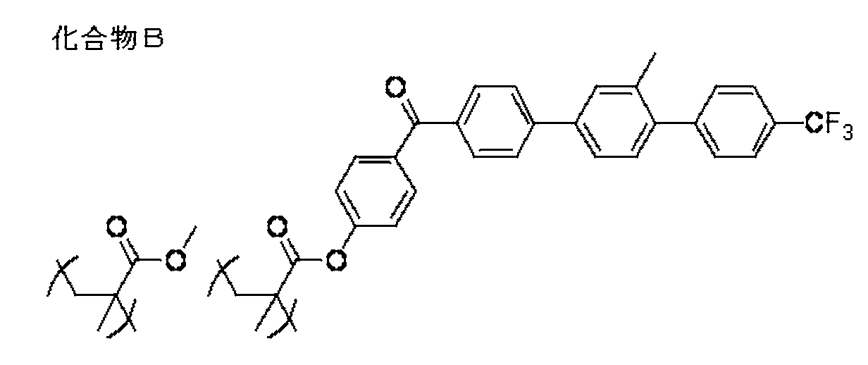
<化合物Bの合成法> なお、化合物Bは以下に示した方法で合成した。

<原料化合物1の合成> アニソール27.0g(250mmol)と4-ブロモベンゾイルクロリド42.9g(200mmol)を塩化メチレン500mlに溶解させ、内温5℃まで冷却した後、6回に分けて塩化アルミニウムを33.4g(250mmol)添加して窒素雰囲気下で8時間攪拌した。反応溶液を水に注ぎ込んだ後に塩化メチレンで抽出し、ロータリーエバポレーターで蒸発乾固させて白色の化合物2を定量的に得た。得られた化合物1は1H NMRにより目的生成物であることを確認した。
<原料化合物2の合成> 原料化合物1 35.0g(120mmol)に対して臭化水素酸140ml、酢酸220mlを加えて内温110℃で12時間半攪拌した。室温まで放冷した後、反応溶液を水に注ぎ込み室温で20分間攪拌した。沈殿をろ過した後に純水、ヘキサン:酢酸エチル=5:1で洗浄し減圧乾燥させて白色の化合物3を定量的に得た。得られた化合物2は1H NMRにより目的生成物であることを確認した。
<原料化合物3の合成> 原料化合物2 9.74g(35.1mmol)をテトラヒドロフラン70mlに溶解させトリエチルアミン7.10g(70.2mmol)を加えて内温5℃まで冷却した。その後メタクリル酸クロリド3.67g(35.1mmol)を滴下しながら窒素雰囲気下で2時間攪拌した。反応溶液を水に注ぎ込み、室温で20分間攪拌した。析出した沈殿をろ別、室温乾燥して白色の化合物3を定量的に得た。得られた化合物3は1H NMRにより目的生成物であることを確認した。
<原料化合物4の合成> 5-ブロモ-2-ヨードトルエン63.5g(214mmol)、パラトリフルオロメチルフェニルボロン酸44.7g(235mmol)、酢酸パラジウム2.40g(10.7mmol)、炭酸ナトリウム68.0g(642mmol)に対して1,2-ジメトキシエタン350ml、水70mlを加え、窒素雰囲気下、外温90℃で72時間攪拌した。室温まで放冷した後、酢酸エチルで抽出しロータリーエバポレーターで濃縮した後にシリカゲルカラム(ヘキサン)で精製して白色の化合物4を57.9g(収率86%)得た。得られた化合物4は1H NMRにより目的生成物であることを確認した。
<原料化合物5の合成> 原料化合物4を57.9g(184mmol)、ビスピナコラートジボロン56.1g(221mmol)、[1、1’-ビス(ジフェニルホスフィノ)フェロセン]パラジウム(II)ジクロリドジクロロメタン付加物4.25g(5.20mmol)、酢酸カリウム54.2g(552mmol)に対してジメチルスルホキシド400mlを加え、窒素雰囲気下、内温90℃で5時間攪拌した。室温まで放冷した後、酢酸エチルで抽出しロータリーエバポレーターで濃縮した後にシリカゲルカラム(ヘキサン:酢酸エチル=10:1)で精製して白色の化合物5を57.5g(収率86%)得た。得られた化合物5は1H NMRにより目的生成物であることを確認した。
<原料化合物6の合成> 原料化合物3を14.8g(42.9mmol)、原料化合物5を18.6g(51.5mmol)、テトラキストリフェニルホスフィンパラジウム2.48g(2.15mmol)、炭酸カリウム17.8g(129mmol)、ジブチルヒドロキシトルエン1mgに対してトルエン170ml、水20mlを加え、窒素雰囲気下、外温90℃で12時間攪拌した。室温まで放冷した後、酢酸エチルで抽出しロータリーエバポレーターで濃縮した後にシリカゲルカラム(酢酸エチル:ヘキサン=1:5)で精製し、酢酸エチル/ヘキサンで再結晶してろ別・乾燥して白色の化合物6を6.8g(収率32%)得た。得られた化合物6は1H NMRにより目的生成物であることを確認した。1H NMR(CDCl3) 7.92(d,4H)、7.76(dd,2H)、7.71(d,2H)、7.59-7.55(m,2H)、7.50(d,2H)、7.34(d,1H)、7.29(dd,2H)、6.41(s,1H)、5.82(t,1H)、2.37(s,3H)
<化合物Bの合成>
テトラヒドロフラン5gを窒素雰囲気下で外温70℃で攪拌した。そこにテトラヒドロフラン26.7gに溶解させた原料化合物6 2.00g(4.00mmol)、メタクリル酸メチル11.6g(116mmol)、2,2’-アゾビス(2,4-ジメチルバレロニトリル)29.8mg(0.12mmol)を2時間かけて滴下し、その後8時間攪拌した。室温まで放冷した後、アセトンで希釈して、アセトン/ヘキサンで再結晶し、ろ別・乾燥して化合物D-1を4.77g得た。得られたポリマーは1H NMRによって組成を確認し、GPCによって分子量測定を行った。(組成比 原料化合物6/メタクリル酸メチル=12/88(モル比),Mw=367,000)
テトラヒドロフラン5gを窒素雰囲気下で外温70℃で攪拌した。そこにテトラヒドロフラン26.7gに溶解させた原料化合物6 2.00g(4.00mmol)、メタクリル酸メチル11.6g(116mmol)、2,2’-アゾビス(2,4-ジメチルバレロニトリル)29.8mg(0.12mmol)を2時間かけて滴下し、その後8時間攪拌した。室温まで放冷した後、アセトンで希釈して、アセトン/ヘキサンで再結晶し、ろ別・乾燥して化合物D-1を4.77g得た。得られたポリマーは1H NMRによって組成を確認し、GPCによって分子量測定を行った。(組成比 原料化合物6/メタクリル酸メチル=12/88(モル比),Mw=367,000)
<高分子材料層の形成>
得られた塗布液を支持体となるスライドガラスにスピンコートして厚さ1μmの高分子材料層を形成した。
このサンプルを分光光度計(島津製作所製UV-3100PC)で吸光度を測定し、得られた吸光度(λ=405nm)から光吸収率を算出したところ、0%であることを確認した。
得られた塗布液を支持体となるスライドガラスにスピンコートして厚さ1μmの高分子材料層を形成した。
このサンプルを分光光度計(島津製作所製UV-3100PC)で吸光度を測定し、得られた吸光度(λ=405nm)から光吸収率を算出したところ、0%であることを確認した。
<回折格子の形成>
記録用レーザとして、波長405nm、パルス幅2.0ps、繰り返し速度76MHzのパルスレーザを用いた。レーザ照射エネルギの制御には、光路中に電気光学変調器(EOM)を使用してパルス強度を制御した。対物レンズとしてはNA0.85の無限遠対物レンズ(倍率×60)を使用した。パルスレーザを、高分子材料層表面でのピークパワーが60Wになるように設定し300nm間隔のドットが形成されるように照射パルス数をEOMにて制御した。加工後の高分子材料層表面をAFMにて観察したところ、図22のAFM像および図23の断面プロファイルに示すように、高さ約30~40nmの突起が形成されていることを確認し、微小な位相変調用のピクセルを加工可能であることを確認した。
記録用レーザとして、波長405nm、パルス幅2.0ps、繰り返し速度76MHzのパルスレーザを用いた。レーザ照射エネルギの制御には、光路中に電気光学変調器(EOM)を使用してパルス強度を制御した。対物レンズとしてはNA0.85の無限遠対物レンズ(倍率×60)を使用した。パルスレーザを、高分子材料層表面でのピークパワーが60Wになるように設定し300nm間隔のドットが形成されるように照射パルス数をEOMにて制御した。加工後の高分子材料層表面をAFMにて観察したところ、図22のAFM像および図23の断面プロファイルに示すように、高さ約30~40nmの突起が形成されていることを確認し、微小な位相変調用のピクセルを加工可能であることを確認した。
Claims (17)
- 高分子材料層を有する回折光学素子であって、
該高分子材料層は、高分子材料と、前記高分子材料層中に分散され、または、前記高分子材料層中の前記高分子材料に共有結合された色素とを有し、
前記高分子材料層の界面に、ドット状の開口および/または凸部による回折光学素子パターンが配列されてなることを特徴とする回折光学素子。 - 前記色素は、1光子吸収色素を含むことを特徴とする請求項1に記載の回折光学素子。
- 前記色素は、多光子吸収色素を含むことを特徴とする請求項1に記載の回折光学素子。
- 前記高分子材料層を支持する支持体を有することを特徴とする請求項1に記載の回折光学素子。
- 前記高分子材料層の前記開口および/または前記凸部が配列された側に、カバー層を備えることを特徴とする請求項1に記載の回折光学素子。
- 前記開口および/または前記凸部は、深さまたは高さの異なる複数種類があり、当該複数種類の開口および/または凸部により、多値の回折光学素子パターンが形成されていることを特徴とする請求項1に記載の回折光学素子。
- 前記色素は、吸収波長帯域が、主として450nm以下にあり、かつ、450~800nmの波長の光透過率が50%以上であることを特徴とする請求項1に記載の回折光学素子。
- 色素が分散された高分子材料または色素が共有結合された高分子材料を有する高分子材料層を準備し、
前記高分子材料層の界面近傍に前記色素が吸収する波長のレーザ光を照射して前記界面を変形させ、この照射を前記界面において所定のパターンで行うことで前記界面に回折光学素子パターンを構成するドット状の開口および/または凸部を形成することを特徴とする回折光学素子の製造方法。 - 1つの前記開口または前記凸部を形成するためのレーザ光の照射時間が120μsec以下であることを特徴とする請求項8に記載の回折光学素子の製造方法。
- レーザ光の照射中に、前記界面からの反射光をセンサにより検出し、当該センサの出力信号に基づいてレーザ光の焦点位置を所定位置に調整することを特徴とする請求項8に記載の回折光学素子の製造方法。
- 色素が分散された高分子材料または色素が共有結合された高分子材料を有する高分子材料層に回折光学素子パターンを形成するための回折光学素子の製造装置であって、
前記色素が吸収する波長のレーザ光を発する光源と、
前記光源から出射されたレーザ光を偏向させる偏向器と、
前記偏向器で偏向されたレーザ光を前記高分子材料層の界面近傍に結像させるための結像光学系と、
前記光源の出力および前記偏向器を制御する制御装置とを備え、
前記制御装置は、前記高分子材料層の界面に回折光学素子パターンを構成するドット状の開口および/または凸部を形成するように、前記偏向器を制御して前記高分子材料層の界面にレーザ光を走査するのに同期させて、前記光源の出力を変化させるように構成されたことを特徴とする回折光学素子の製造装置。 - 前記結像光学系は、対物レンズと、少なくとも2枚の集光レンズとを含むことを特徴とする請求項11に記載の回折光学素子の製造装置。
- 1つの前記開口または前記凸部を形成するためのレーザ光の照射時間が120μsec以下であることを特徴とする請求項11に記載の回折光学素子の製造装置。
- 前記結像光学系は対物レンズを含み、当該対物レンズは、開口数が0.13以上であることを特徴とする請求項11に記載の回折光学素子の製造装置。
- 前記界面で反射したレーザ光を検出するセンサをさらに備え、
前記制御装置は、前記センサの出力信号に基づいて前記結像光学系を制御してレーザ光の焦点位置を所定位置に調整するように構成されたことを特徴とする請求項11に記載の回折光学素子の製造装置。 - 前記光源が発するレーザ光の波長が450nm以下であることを特徴とする請求項11に記載の回折光学素子の製造装置。
- 前記高分子材料層を、レーザ光に対して移動させる搬送装置を有することを特徴とする請求項11に記載の回折光学素子の製造装置。
Applications Claiming Priority (2)
| Application Number | Priority Date | Filing Date | Title |
|---|---|---|---|
| JP2012213635 | 2012-09-27 | ||
| JP2012-213635 | 2012-09-27 |
Publications (1)
| Publication Number | Publication Date |
|---|---|
| WO2014050308A1 true WO2014050308A1 (ja) | 2014-04-03 |
Family
ID=50387722
Family Applications (1)
| Application Number | Title | Priority Date | Filing Date |
|---|---|---|---|
| PCT/JP2013/070992 Ceased WO2014050308A1 (ja) | 2012-09-27 | 2013-08-02 | 回折光学素子ならびに回折光学素子の製造方法および製造装置 |
Country Status (1)
| Country | Link |
|---|---|
| WO (1) | WO2014050308A1 (ja) |
Citations (7)
| Publication number | Priority date | Publication date | Assignee | Title |
|---|---|---|---|---|
| JPH0798870B2 (ja) * | 1987-12-11 | 1995-10-25 | 帝人株式会社 | 高分子の光加工方法 |
| JP2005099416A (ja) * | 2003-09-25 | 2005-04-14 | Fuji Photo Film Co Ltd | ホログラム記録方法及びホログラム記録材料 |
| JP2007057622A (ja) * | 2005-08-22 | 2007-03-08 | Ricoh Co Ltd | 光学素子及びその製造方法、光学素子用形状転写型の製造方法及び光学素子用転写型 |
| WO2007043451A1 (ja) * | 2005-10-05 | 2007-04-19 | Pioneer Corporation | ホログラム記録再生システム |
| JP2007212485A (ja) * | 2006-02-07 | 2007-08-23 | Ricoh Co Ltd | 光学素子、マルチビーム光源ユニット、光走査装置及び画像形成装置 |
| WO2009050857A1 (ja) * | 2007-10-15 | 2009-04-23 | Fujifilm Corporation | 凹部形成方法、凹凸製品の製造方法、発光素子の製造方法および光学素子の製造方法 |
| JP2011095465A (ja) * | 2009-10-29 | 2011-05-12 | Toppan Printing Co Ltd | 表示体 |
-
2013
- 2013-08-02 WO PCT/JP2013/070992 patent/WO2014050308A1/ja not_active Ceased
Patent Citations (7)
| Publication number | Priority date | Publication date | Assignee | Title |
|---|---|---|---|---|
| JPH0798870B2 (ja) * | 1987-12-11 | 1995-10-25 | 帝人株式会社 | 高分子の光加工方法 |
| JP2005099416A (ja) * | 2003-09-25 | 2005-04-14 | Fuji Photo Film Co Ltd | ホログラム記録方法及びホログラム記録材料 |
| JP2007057622A (ja) * | 2005-08-22 | 2007-03-08 | Ricoh Co Ltd | 光学素子及びその製造方法、光学素子用形状転写型の製造方法及び光学素子用転写型 |
| WO2007043451A1 (ja) * | 2005-10-05 | 2007-04-19 | Pioneer Corporation | ホログラム記録再生システム |
| JP2007212485A (ja) * | 2006-02-07 | 2007-08-23 | Ricoh Co Ltd | 光学素子、マルチビーム光源ユニット、光走査装置及び画像形成装置 |
| WO2009050857A1 (ja) * | 2007-10-15 | 2009-04-23 | Fujifilm Corporation | 凹部形成方法、凹凸製品の製造方法、発光素子の製造方法および光学素子の製造方法 |
| JP2011095465A (ja) * | 2009-10-29 | 2011-05-12 | Toppan Printing Co Ltd | 表示体 |
Similar Documents
| Publication | Publication Date | Title |
|---|---|---|
| Kato et al. | Multiple-spot parallel processing for laser micronanofabrication | |
| RU2514152C2 (ru) | Оптический элемент, устройство отображения, противоотражающий оптический компонент и мастер-форма | |
| JP5476329B2 (ja) | 光情報記録媒体 | |
| US8980530B2 (en) | Optical information recording medium and method for recording information in optical information recording medium | |
| CN103168329A (zh) | 光学信息记录介质 | |
| TWI454863B (zh) | 全像儲存方法 | |
| US20090075014A1 (en) | Optical recording method and reproducing method | |
| Jiang et al. | Solvent-free optical recording of structural colours on pre-imprinted photocrosslinkable nanostructures | |
| US7964333B1 (en) | FRET-based two photon three dimensional optical data storage | |
| Lu et al. | Fabrication of a multifaceted mapping mirror using two-photon polymerization for a snapshot image mapping spectrometer | |
| WO2014050308A1 (ja) | 回折光学素子ならびに回折光学素子の製造方法および製造装置 | |
| Scott et al. | Principles of voxel refinement in optical direct write lithography | |
| JP2000047046A (ja) | 屈折率分布型光学成形体の製造方法 | |
| US9792944B2 (en) | Recording material and optical information recording medium | |
| Nakata et al. | Sub-micron period metal lattices fabricated by interfering ultraviolet femtosecond laser processing | |
| CN101582269A (zh) | 聚焦光学系统和光盘母盘曝光装置 | |
| JP4906371B2 (ja) | 二光子吸収材料及びその用途 | |
| JP4368148B2 (ja) | フィルム、フィルムを用いた光メモリ材料、および、フィルムの製造方法 | |
| JP4963367B2 (ja) | 二光子吸収材料 | |
| JPWO2017082357A1 (ja) | 超解像顕微鏡 | |
| JP5505748B2 (ja) | π共役系化合物とその用途、およびそれらを用いた素子、装置 | |
| JP2009191094A (ja) | 光記録用化合物、光記録用組成物およびホログラフィック記録媒体 | |
| JP2008069294A (ja) | π共役系化合物とその用途、およびそれらを用いた素子、装置 | |
| JP2013225113A (ja) | フォトリフラクティブ基材およびホログラム記録媒体 | |
| JP4969881B2 (ja) | 二光子吸収材料とその用途 |
Legal Events
| Date | Code | Title | Description |
|---|---|---|---|
| 121 | Ep: the epo has been informed by wipo that ep was designated in this application |
Ref document number: 13840782 Country of ref document: EP Kind code of ref document: A1 |
|
| NENP | Non-entry into the national phase |
Ref country code: DE |
|
| 122 | Ep: pct application non-entry in european phase |
Ref document number: 13840782 Country of ref document: EP Kind code of ref document: A1 |
|
| NENP | Non-entry into the national phase |
Ref country code: JP |