以下の実施の形態においては便宜上その必要があるときは、複数のセクションまたは実施の形態に分割して説明するが、特に明示した場合を除き、それらはお互いに無関係なものではなく、一方は他方の一部または全部の変形例、詳細、補足説明等の関係にある。
In the following embodiments, when it is necessary for the sake of convenience, the description will be divided into a plurality of sections or embodiments. However, unless otherwise specified, they are not irrelevant to each other. There are some or all of the modifications, details, supplementary explanations, and the like.
また、以下の実施の形態において、要素の数等(個数、数値、量、範囲等を含む)に言及する場合、特に明示した場合および原理的に明らかに特定の数に限定される場合等を除き、その特定の数に限定されるものではなく、特定の数以上でも以下でもよい。
Further, in the following embodiments, when referring to the number of elements (including the number, numerical value, quantity, range, etc.), especially when clearly indicated and when clearly limited to a specific number in principle, etc. Except, it is not limited to the specific number, and may be more or less than the specific number.
さらに、以下の実施の形態において、その構成要素(要素ステップ等も含む)は、特に明示した場合および原理的に明らかに必須であると考えられる場合等を除き、必ずしも必須のものではないことはいうまでもない。同様に、以下の実施の形態において、構成要素等の形状、位置関係等に言及するときは、特に明示した場合および原理的に明らかにそうでないと考えられる場合等を除き、実質的にその形状等に近似または類似するもの等を含むものとする。このことは、上記数値および範囲についても同様である。
Further, in the following embodiments, the constituent elements (including element steps and the like) are not necessarily indispensable unless otherwise specified and apparently essential in principle. Needless to say. Similarly, in the following embodiments, when referring to the shapes, positional relationships, etc. of the components, etc., the shapes are substantially the same unless otherwise specified, or otherwise apparent in principle. And the like are included. The same applies to the above numerical values and ranges.
以下、本発明の実施の形態を図面に基づいて詳細に説明する。なお、実施の形態を説明するための全図において、同一の機能を有する部材には同一の符号を付し、その繰り返しの説明は省略する。また、以下の実施の形態では、特に必要なとき以外は同一または同様な部分の説明を原則として繰り返さない。
Hereinafter, embodiments of the present invention will be described in detail with reference to the drawings. Note that components having the same function are denoted by the same reference symbols throughout the drawings for describing the embodiments, and the repetitive description thereof will be omitted. In the following embodiments, the description of the same or similar parts will not be repeated in principle unless particularly necessary.
さらに、実施の形態で用いる図面においては、断面図であっても図面を見やすくするためにハッチングを省略する場合もある。また、平面図であっても図面を見やすくするためにハッチングを付す場合もある。
Furthermore, in the drawings used in the embodiments, hatching may be omitted even in a cross-sectional view for easy viewing of the drawings. Further, even a plan view may be hatched to make the drawing easy to see.
なお、以下に説明する各実施の形態では、荷電粒子線装置を、一次荷電粒子線として電子線を用いた走査型電子顕微鏡(SEM)からなる荷電粒子線顕微鏡に適用した場合を例に挙げて説明を行う。しかし、各実施の形態は、一次荷電粒子線としてイオンビームを試料に照射し、二次的に発生した二次電子や反射電子を検出するSIM(Scanning Ion Microscope)またはイオンビームを使用したイオン顕微鏡など、他の各種の荷電粒子線装置に適用可能である。また、以下に説明する各実施の形態は、本発明の要旨を逸脱しない範囲で適宜組み合わせることが可能である。
In each embodiment described below, the charged particle beam apparatus is applied as an example to a charged particle beam microscope including a scanning electron microscope (SEM) using an electron beam as a primary charged particle beam. Give an explanation. However, each embodiment irradiates a sample with an ion beam as a primary charged particle beam, and detects a secondary electron or a reflected electron generated by a SIM (Scanning Ion Microscope) or an ion microscope using an ion beam. It is applicable to other various charged particle beam devices. The embodiments described below can be combined as appropriate without departing from the scope of the present invention.
(実施の形態1)
<荷電粒子線装置の構成>
本発明の一実施の形態である荷電粒子線装置を、図面を参照して説明する。前述したように、以下では、荷電粒子線装置をSEMに適用した例について説明する。
(Embodiment 1)
<Configuration of charged particle beam device>
A charged particle beam apparatus according to an embodiment of the present invention will be described with reference to the drawings. As described above, an example in which the charged particle beam apparatus is applied to an SEM will be described below.
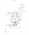
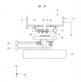
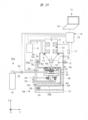
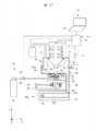
図1は、実施の形態1の荷電粒子線装置の全体構成図である。
FIG. 1 is an overall configuration diagram of the charged particle beam apparatus according to the first embodiment.
図1に示すように、荷電粒子線装置1には、荷電粒子光学鏡筒2および筐体3が設けられている。荷電粒子光学鏡筒2および筐体3により、真空室4が区画されている。
As shown in FIG. 1, the charged particle beam apparatus 1 is provided with a charged particle optical column 2 and a housing 3. A vacuum chamber 4 is defined by the charged particle optical column 2 and the housing 3.
荷電粒子光学鏡筒2は、例えば筐体3の上側に、荷電粒子光学鏡筒2の下部が筐体3の内部に突出するように、設けられている。荷電粒子光学鏡筒2は、シール部材(Oリング)5を介して筐体3に取り付けられており、荷電粒子光学鏡筒2および筐体3により区画された真空室4は、気密に設けられている。
The charged particle optical column 2 is provided, for example, on the upper side of the casing 3 so that the lower part of the charged particle optical column 2 protrudes into the casing 3. The charged particle optical column 2 is attached to the housing 3 via a seal member (O-ring) 5, and the vacuum chamber 4 partitioned by the charged particle optical column 2 and the housing 3 is airtightly provided. ing.
荷電粒子光学鏡筒2および筐体3により区画された真空室4の外部には、真空ポンプ(排気部)6が設けられている。真空ポンプ6は、荷電粒子光学鏡筒2および筐体3に、真空配管7により接続されている。すなわち、真空ポンプ6は、真空室4に接続されている。
A vacuum pump (exhaust unit) 6 is provided outside the vacuum chamber 4 partitioned by the charged particle optical column 2 and the housing 3. The vacuum pump 6 is connected to the charged particle optical barrel 2 and the housing 3 by a vacuum pipe 7. That is, the vacuum pump 6 is connected to the vacuum chamber 4.
荷電粒子線装置1の使用時には、真空室4は、真空ポンプ6により排気され、真空室4の内部の圧力が真空に減圧される。すなわち、真空室4は、真空ポンプ6により排気され、真空室4の内部の圧力が、真空室4の外部の圧力よりも減圧された状態に、維持される。
When using the charged particle beam apparatus 1, the vacuum chamber 4 is evacuated by the vacuum pump 6, and the pressure inside the vacuum chamber 4 is reduced to a vacuum. That is, the vacuum chamber 4 is evacuated by the vacuum pump 6, and the pressure inside the vacuum chamber 4 is maintained in a state where the pressure is reduced more than the pressure outside the vacuum chamber 4.
なお、真空ポンプ(排気部)6は1つのみ示されているが、2つ以上あってもよい。
Although only one vacuum pump (exhaust unit) 6 is shown, there may be two or more.
筐体3には、リークバルブ8が設けられている。リークバルブ8は、荷電粒子光学鏡筒2および筐体3により区画された真空室4を大気開放するためのものである。リークバルブ8により、メンテナンス時などに、筐体3の内部を大気開放することができる。リークバルブ8は、なくてもよいし、2つ以上あってもよい。また、筐体3におけるリークバルブ8の配置箇所は、図1に示された場所に限られない。すなわち、リークバルブ8は、筐体3の別の位置に配置されていてもよい。
The casing 3 is provided with a leak valve 8. The leak valve 8 is for opening the vacuum chamber 4 defined by the charged particle optical column 2 and the housing 3 to the atmosphere. The leak valve 8 can open the interior of the housing 3 to the atmosphere during maintenance or the like. The leak valve 8 may be omitted or may be two or more. Moreover, the arrangement | positioning location of the leak valve 8 in the housing | casing 3 is not restricted to the location shown by FIG. That is, the leak valve 8 may be arranged at another position of the housing 3.
荷電粒子光学鏡筒2の内部には、荷電粒子源9および荷電粒子光学系10が設けられている。荷電粒子源9は、荷電粒子線を発生させる。荷電粒子線装置1がSEMであるときは、荷電粒子源9は電子線を発生させる電子源であり、例えばフィラメントを含む電子銃からなる。荷電粒子光学系10は、光学レンズ11などの要素により構成されている。荷電粒子光学系10は、荷電粒子源9により発生した荷電粒子線を集束して試料12に照射し、一次荷電粒子線として試料12上を走査する。すなわち、荷電粒子光学系10は、荷電粒子源9により発生した荷電粒子線を、試料12に走査して照射する。
A charged particle source 9 and a charged particle optical system 10 are provided inside the charged particle optical column 2. The charged particle source 9 generates a charged particle beam. When the charged particle beam apparatus 1 is an SEM, the charged particle source 9 is an electron source that generates an electron beam, and includes, for example, an electron gun including a filament. The charged particle optical system 10 includes elements such as an optical lens 11. The charged particle optical system 10 focuses the charged particle beam generated by the charged particle source 9 and irradiates the sample 12 to scan the sample 12 as a primary charged particle beam. That is, the charged particle optical system 10 scans and irradiates the sample 12 with the charged particle beam generated by the charged particle source 9.
荷電粒子光学鏡筒2のうち筐体3の内部に突出した部分には、検出器13が設けられている。検出器13は、試料12に一次荷電粒子線を照射することで、試料12から放出される(発生する)二次荷電粒子(二次電子または反射電子)を検出する。検出器13は、例えば数keV~数十keVのエネルギーで飛来してくる荷電粒子を増幅して検知することができる。検出器13は、薄くて平らであることが好ましいので、検出器13として、例えば、シリコン等の半導体材料で作られた半導体検出器や、ガラス面あるいは内部にて荷電粒子による信号を光に変換することが可能なシンチレータ等を用いることができる。
A detector 13 is provided on a portion of the charged particle optical column 2 that protrudes into the housing 3. The detector 13 irradiates the sample 12 with a primary charged particle beam, thereby detecting secondary charged particles (secondary electrons or reflected electrons) emitted (generated) from the sample 12. The detector 13 can amplify and detect charged particles flying with energy of several keV to several tens keV, for example. Since the detector 13 is preferably thin and flat, the detector 13 is, for example, a semiconductor detector made of a semiconductor material such as silicon, or a signal from charged particles on the glass surface or inside is converted into light. A scintillator or the like that can be used can be used.
さらに、本実施の形態1の荷電粒子線装置1には、制御系14として、制御部15およびパーソナルコンピュータ16が設けられている。制御部15は、真空ポンプ(排気部)6および荷電粒子光学系10などの制御を行う。パーソナルコンピュータ16は、荷電粒子線装置1を操作するための操作画面(Graphical User Interface:GUI)が表示されるモニタと、キーボードやマウスなど使用者からの操作画面へのコマンドを入力するための入力部とを備えている。パーソナルコンピュータ16は、制御部15と通信線により接続される。なお、制御部15はアナログ回路やディジタル回路を内蔵しており、真空ポンプ6、荷電粒子源9、光学レンズ11および検出器13の出力信号を、ディジタル画像信号に変換して、パーソナルコンピュータ16へ送信する。
Furthermore, in the charged particle beam apparatus 1 of the first embodiment, a control unit 15 and a personal computer 16 are provided as the control system 14. The control unit 15 controls the vacuum pump (exhaust unit) 6 and the charged particle optical system 10. The personal computer 16 has a monitor on which an operation screen (Graphical User Interface: GUI) for operating the charged particle beam apparatus 1 is displayed, and an input for inputting commands to the operation screen from the user such as a keyboard and a mouse. Department. The personal computer 16 is connected to the control unit 15 through a communication line. The control unit 15 includes an analog circuit and a digital circuit, and converts the output signals of the vacuum pump 6, the charged particle source 9, the optical lens 11, and the detector 13 into digital image signals and supplies them to the personal computer 16. Send.
図1に示すように、検出器13は、例えばプリアンプなどの増幅器17を経由して制御部15に接続されていてもよく、このとき、検出器13からの出力信号は、例えば増幅器17を経由して制御部15に送られる。あるいは、増幅器17が不要であれば、検出器13からの出力信号は、増幅器17を経由して制御部15に送られなくてもよい。
As shown in FIG. 1, the detector 13 may be connected to the control unit 15 via an amplifier 17 such as a preamplifier. At this time, an output signal from the detector 13 passes through the amplifier 17, for example. And sent to the control unit 15. Alternatively, if the amplifier 17 is unnecessary, the output signal from the detector 13 may not be sent to the control unit 15 via the amplifier 17.
なお、図1に示す制御系14の構成は一例に過ぎない。したがって、制御部15や真空配管7の途中に設けられるバルブ(図示は省略)、真空ポンプ6または各通信線などについての変形例は、本実施の形態1の要旨を逸脱しない限り、本実施の形態1の荷電粒子線装置の範囲に属する。
Note that the configuration of the control system 14 shown in FIG. 1 is merely an example. Therefore, the modified examples of the valve (not shown), the vacuum pump 6 or each communication line provided in the middle of the control unit 15 and the vacuum pipe 7 are not limited to the present embodiment unless departing from the gist of the first embodiment. It belongs to the range of the charged particle beam apparatus of aspect 1.
<真空室の外部>
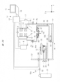
図2は、実施の形態1の荷電粒子線装置のうち、隔膜素子および試料ステージの周辺の構造を示す図である。
<Outside of vacuum chamber>
FIG. 2 is a diagram illustrating a structure around the diaphragm element and the sample stage in the charged particle beam apparatus according to the first embodiment.
筐体3には、隔膜素子(隔膜部材)18aが設けられている。図1および図2に示す例では、筐体3の下面部(真空室4の壁部)3aであって、荷電粒子光学鏡筒2の下方に位置する部分に、隔膜素子18aが設けられている。隔膜素子18aの詳細な構造については後述するが、隔膜素子18aは、一次荷電粒子線を透過または通過させる隔膜(メンブレン、膜部)19を含み、真空室4の内部の空間と、真空室4の外部の空間とを、気密に隔離する。
The casing 3 is provided with a diaphragm element (diaphragm member) 18a. In the example shown in FIG. 1 and FIG. 2, a diaphragm element 18 a is provided on the lower surface portion (wall portion of the vacuum chamber 4) 3 a of the housing 3, which is located below the charged particle optical column 2. Yes. Although the detailed structure of the diaphragm element 18a will be described later, the diaphragm element 18a includes a diaphragm (membrane, film part) 19 that transmits or passes the primary charged particle beam, and the space inside the vacuum chamber 4 and the vacuum chamber 4 Airtight isolation from the outside space.
筐体3の下面部3aであって、荷電粒子光学鏡筒2の下方に位置する部分には、一次荷電粒子線を透過または通過させるための開口部3bが形成されており、開口部3bを塞ぐように、隔膜素子18aが取り付けられている。隔膜素子18aの中央部には、一次荷電粒子線を透過または通過させるための隔膜(膜部)19が形成されている。隔膜素子18aは、隔膜19の周囲の部分が、接着部材21により、筐体3の下面部3aであって、開口部3bの周囲の部分に接着されることで、筐体3の下面部3aに取り付けられている。
An opening 3b for transmitting or passing the primary charged particle beam is formed in a lower surface portion 3a of the housing 3 and below the charged particle optical column 2. The opening 3b is formed through the opening 3b. The diaphragm element 18a is attached so as to close it. In the central part of the diaphragm element 18a, a diaphragm (film part) 19 for transmitting or passing the primary charged particle beam is formed. In the diaphragm element 18a, the peripheral portion of the diaphragm 19 is bonded to the lower surface portion 3a of the housing 3 and the peripheral portion of the opening 3b by the adhesive member 21, so that the lower surface portion 3a of the housing 3 is bonded. Is attached.
接着部材21は、好適には、隔膜素子18aと筐体3の下面部3aとの間を気密にシールする。接着部材21は、荷電粒子線装置1の使用時に、真空室4の内部の圧力が真空室4の外部の圧力よりも減圧された状態で、隔膜素子18aと筐体3の下面部3aとの間を気密にシールするものである。また、接着部材21は、荷電粒子線装置1のメンテナンス時に、真空室4の内部を大気圧に戻した状態でも、隔膜素子18aが筐体3の下面部3aから剥がれ落ちないように接着するものである。このようなシール力および接着力を有する接着部材21として、例えばシリコンゴム、銀ペースト、真空グリース、エポキシ樹脂またはシリコーン樹脂などの材料を含むものを用いることができる。
The adhesive member 21 preferably hermetically seals between the diaphragm element 18 a and the lower surface portion 3 a of the housing 3. When the charged particle beam apparatus 1 is used, the adhesive member 21 is formed between the diaphragm element 18a and the lower surface portion 3a of the housing 3 in a state where the pressure inside the vacuum chamber 4 is lower than the pressure outside the vacuum chamber 4. The space is hermetically sealed. Further, the adhesive member 21 adheres so that the diaphragm element 18a does not peel off from the lower surface portion 3a of the housing 3 even when the inside of the vacuum chamber 4 is returned to atmospheric pressure during maintenance of the charged particle beam apparatus 1. It is. As the adhesive member 21 having such a sealing force and adhesive force, for example, a member containing a material such as silicon rubber, silver paste, vacuum grease, epoxy resin, or silicone resin can be used.
荷電粒子光学鏡筒2および筐体3により区画された真空室4の外部であって、隔膜素子18aの下方に位置する部分には、試料ステージ(保持部)22が設けられている。試料ステージ22は、真空室4の外部で試料12を保持するためのものである。試料ステージ22は、台座23上に組み立てられている。
A sample stage (holding unit) 22 is provided outside the vacuum chamber 4 defined by the charged particle optical column 2 and the housing 3 and below the diaphragm element 18a. The sample stage 22 is for holding the sample 12 outside the vacuum chamber 4. The sample stage 22 is assembled on the pedestal 23.
また、真空室4の外部には、Z軸駆動部24およびX、Y軸駆動部25が設けられている。Z軸駆動部24は、試料ステージ22を例えば鉛直方向であるZ軸方向に移動駆動し、試料ステージ22の高さ位置を変えることで、試料ステージ22に保持されている試料12と隔膜素子18aとのZ軸方向に沿った距離を調整する。X、Y軸駆動部25は、試料ステージ22を例えば水平面内で互いに交差する2方向であるX軸方向およびY軸方向に移動駆動することで、試料ステージ22に保持されている試料12を、X軸方向およびY軸方向に移動させる。
In addition, a Z-axis drive unit 24 and an X and Y-axis drive unit 25 are provided outside the vacuum chamber 4. The Z-axis drive unit 24 moves and drives the sample stage 22 in, for example, the vertical Z-axis direction, and changes the height position of the sample stage 22, whereby the sample 12 and the diaphragm element 18 a held on the sample stage 22 are changed. The distance along the Z-axis direction is adjusted. The X and Y axis driving unit 25 moves and drives the sample stage 22 in, for example, the X axis direction and the Y axis direction, which are two directions intersecting each other in a horizontal plane, whereby the sample 12 held on the sample stage 22 is moved. Move in the X-axis direction and the Y-axis direction.
荷電粒子線装置1の使用時には、試料12を試料ステージ22上に載せた状態で保持し、Z軸駆動部24を用いて、試料12が鮮明に観察されるように、試料12の高さ位置を調整する。また、X、Y軸駆動部25を調整することにより、試料12の画像を観察しながら所望の場所に移動させる。
When the charged particle beam apparatus 1 is used, the height position of the sample 12 is held so that the sample 12 is held on the sample stage 22 and the sample 12 is clearly observed using the Z-axis drive unit 24. Adjust. Further, by adjusting the X and Y axis driving unit 25, the X axis and Y axis driving unit 25 is moved to a desired place while observing the image of the sample 12.
なお、本実施の形態1では、Z軸駆動部24が、試料ステージ22を移動駆動することで、試料ステージ22に保持されている試料12と隔膜素子18aとのZ軸方向に沿った距離を調整する。しかし、Z軸駆動部24が、試料ステージ22ではなく、例えば筐体3とともに隔膜素子18aを移動駆動することで、試料ステージ22に保持されている試料12と隔膜素子18aとのZ軸方向に沿った距離を調整することもできる。
In the first embodiment, the Z-axis drive unit 24 moves and drives the sample stage 22, thereby increasing the distance along the Z-axis direction between the sample 12 held on the sample stage 22 and the diaphragm element 18 a. adjust. However, the Z-axis drive unit 24 moves the diaphragm element 18a together with the housing 3, for example, instead of the sample stage 22, so that the sample 12 held on the sample stage 22 and the diaphragm element 18a are moved in the Z-axis direction. You can also adjust the distance along.
本実施の形態1の荷電粒子線装置1では、荷電粒子光学鏡筒2、筐体3により区画され、気密に設けられた真空室4を真空ポンプ(排気部)6により排気することで、真空室4の内部の圧力が、試料12が配置された空間の圧力よりも減圧された状態に、維持する。そして、真空室4の内部と試料12が配置された空間との間に圧力差が存在する状態で、真空室4の内部を通り、筐体3に設けられた隔膜素子18aを透過した一次荷電粒子線を、真空室4の外部で保持されている試料12に走査して照射する。
In the charged particle beam apparatus 1 according to the first embodiment, a vacuum chamber 4 partitioned by the charged particle optical column 2 and the housing 3 and hermetically provided is evacuated by a vacuum pump (exhaust unit) 6, thereby providing a vacuum. The pressure inside the chamber 4 is maintained in a state where the pressure is reduced more than the pressure of the space in which the sample 12 is disposed. Then, in a state where there is a pressure difference between the inside of the vacuum chamber 4 and the space where the sample 12 is disposed, the primary charge that has passed through the inside of the vacuum chamber 4 and transmitted through the diaphragm element 18 a provided in the housing 3. The particle beam scans and irradiates the sample 12 held outside the vacuum chamber 4.
<隔膜素子>
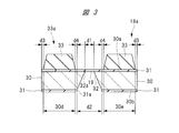
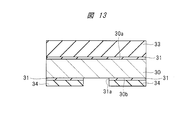
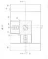
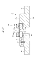
図3は、実施の形態1の隔膜素子の要部断面図である。図4は、実施の形態1の隔膜素子を試料側から見た平面図である。なお、図3は、図4のA-A線に沿った要部断面図である。また、図3では、隔膜素子18aは、筐体3の下面部(真空室4の壁部)3a(図2参照)に取り付けられているときと上下反転した状態で、図示されている。
<Diaphragm element>
FIG. 3 is a cross-sectional view of a main part of the diaphragm element according to the first embodiment. FIG. 4 is a plan view of the diaphragm element according to Embodiment 1 as viewed from the sample side. FIG. 3 is a cross-sectional view of the main part along the line AA in FIG. In FIG. 3, the diaphragm element 18 a is illustrated in a state where the diaphragm element 18 a is turned upside down when attached to the lower surface portion (wall portion of the vacuum chamber 4) 3 a (see FIG. 2) of the housing 3.
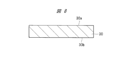
隔膜素子(隔膜部材)18aは、隔膜素子18aの全体を支持する基体として、保持基板(基体)30を含む。保持基板30は、主面30a、および、主面30aと反対側の面である主面30bを有する。主面30aは、隔膜素子18aが筐体3の下面部3a(図2参照)に取り付けられたときに、真空室4の外部に面する。
The diaphragm element (diaphragm member) 18a includes a holding substrate (substrate) 30 as a base that supports the entire diaphragm element 18a. The holding substrate 30 has a main surface 30a and a main surface 30b that is a surface opposite to the main surface 30a. The main surface 30a faces the outside of the vacuum chamber 4 when the diaphragm element 18a is attached to the lower surface portion 3a of the housing 3 (see FIG. 2).
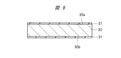
保持基板30の主面30aおよび主面30bには、すなわち保持基板30の両面には、薄膜31が形成されている。保持基板30の主面30bに形成された薄膜31には、薄膜31を貫通して保持基板30に達する開口部31aが形成されており、開口部31aにおいて、保持基板30が除去されて主面30bから主面30aに到達する貫通孔32が形成されている。保持基板30の主面30aに形成された薄膜31のうち、主面30aにおける貫通孔32の開口32aを覆うように残されている部分は、前述した隔膜(メンブレン、膜部)19となる。すなわち、隔膜19は、主面30a上に、主面30aにおける貫通孔32の開口32aを覆うように形成されている。
The thin film 31 is formed on the main surface 30 a and the main surface 30 b of the holding substrate 30, that is, on both surfaces of the holding substrate 30. The thin film 31 formed on the main surface 30b of the holding substrate 30 is formed with an opening 31a that penetrates the thin film 31 and reaches the holding substrate 30. In the opening 31a, the holding substrate 30 is removed and the main surface is removed. A through hole 32 that reaches the main surface 30a from 30b is formed. Of the thin film 31 formed on the main surface 30 a of the holding substrate 30, the portion left so as to cover the opening 32 a of the through hole 32 in the main surface 30 a becomes the above-described diaphragm (membrane, film portion) 19. That is, the diaphragm 19 is formed on the main surface 30a so as to cover the opening 32a of the through hole 32 in the main surface 30a.
また、好適には、開口部31aは、平面視において、保持基板30の主面30bのうち中央部に相当する位置に形成されており、貫通孔32は、平面視において、保持基板30の中央部に形成されている。すなわち、隔膜19は、平面視において、保持基板30の主面30aの中央部に形成されている。貫通孔32が保持基板30の中央部に形成されることで、隔膜素子18aの強度を向上させることができる。
Preferably, the opening 31a is formed at a position corresponding to the central portion of the main surface 30b of the holding substrate 30 in plan view, and the through hole 32 is in the center of the holding substrate 30 in plan view. It is formed in the part. That is, the diaphragm 19 is formed at the center of the main surface 30a of the holding substrate 30 in plan view. By forming the through hole 32 in the central portion of the holding substrate 30, the strength of the diaphragm element 18a can be improved.
保持基板(基体)30として、好適には、例えば単結晶シリコン(Si)からなる半導体基板(Si基板)であって、主面30aおよび主面30bの方位、すなわち基板方位が(100)または(110)であるものを用いることができる。これにより、後述するように、アルカリ性水溶液からなるエッチング液を用いた異方性エッチングを行うことで、保持基板30に貫通孔32を容易に形成することができる。また、形成される貫通孔32の側面が(111)面になるため、貫通孔32を形状精度よく形成することができる。さらに、保持基板30として、両面が鏡面に仕上げられた基板を用いることができる。これにより、保持基板30の両面に、容易に加工を施すことができる。
The holding substrate (base body) 30 is preferably a semiconductor substrate (Si substrate) made of, for example, single crystal silicon (Si), and the orientation of the main surface 30a and the main surface 30b, that is, the substrate orientation is (100) or ( 110) can be used. Thereby, as will be described later, the through hole 32 can be easily formed in the holding substrate 30 by performing anisotropic etching using an etching solution made of an alkaline aqueous solution. Moreover, since the side surface of the through hole 32 to be formed is a (111) surface, the through hole 32 can be formed with high shape accuracy. Further, as the holding substrate 30, a substrate whose both surfaces are mirror-finished can be used. Thereby, it is possible to easily process both surfaces of the holding substrate 30.
なお、薄膜31は、保持基板30の主面30aにおいて、図3および図4に示すように、全面に形成されていてもよいが、少なくとも貫通孔32の開口32aを覆うように形成されていればよい。また、以下の説明では、薄膜31のうち、主面30aにおける貫通孔32の開口32aを覆うように形成されている部分のみを隔膜(膜部)19として説明する。
The thin film 31 may be formed on the entire surface of the main surface 30a of the holding substrate 30 as shown in FIGS. 3 and 4, but may be formed so as to cover at least the opening 32a of the through hole 32. That's fine. In the following description, only the part of the thin film 31 formed so as to cover the opening 32a of the through hole 32 in the main surface 30a will be described as the diaphragm (film part) 19.
隔膜19の厚さが薄くなると、隔膜19を、厚さ寸法の精度よく形成することが困難になる。一方、隔膜19の厚さが厚くなると、真空室4の内部を通った一次荷電粒子線および試料12から放出された二次荷電粒子が隔膜19を透過または通過しにくくなり、試料12に到達する(照射される)一次荷電粒子線の量および検出器13に到達する(検出される)二次荷電粒子の量が減少する。したがって、隔膜19の厚さ、すなわち薄膜31の厚さは、好適には、例えば5~50nmとすることができる。
When the thickness of the diaphragm 19 is reduced, it becomes difficult to form the diaphragm 19 with a precise thickness dimension. On the other hand, when the thickness of the diaphragm 19 is increased, the primary charged particle beam passing through the inside of the vacuum chamber 4 and the secondary charged particles emitted from the sample 12 become difficult to pass through or pass through the diaphragm 19 and reach the sample 12. The amount of primary charged particle beams (irradiated) and the amount of secondary charged particles reaching (detected) the detector 13 are reduced. Therefore, the thickness of the diaphragm 19, that is, the thickness of the thin film 31, can be suitably set to 5 to 50 nm, for example.
また、試料12を大気圧下などの非真空状態で観察する場合、隔膜19と試料12との間で一次荷電粒子線および二次荷電粒子が散乱または吸収され、試料12に照射される一次荷電粒子線の量および検出器13により検出される二次荷電粒子の量がさらに減少する。そのため、隔膜19の厚さ(薄膜31の厚さ)は、さらに薄いことが好ましく、例えば20nm以下であることが好ましい。すなわち、隔膜19の厚さ(薄膜31の厚さ)は、さらに好適には、例えば5~20nmである。
When the sample 12 is observed in a non-vacuum state such as under atmospheric pressure, primary charged particle beams and secondary charged particles are scattered or absorbed between the diaphragm 19 and the sample 12, and the primary charge irradiated to the sample 12. The amount of particle beam and the amount of secondary charged particles detected by the detector 13 are further reduced. Therefore, it is preferable that the thickness of the diaphragm 19 (thickness of the thin film 31) is further thinner, for example, 20 nm or less. That is, the thickness of the diaphragm 19 (thickness of the thin film 31) is more preferably 5 to 20 nm, for example.
また、隔膜19が撓んだ場合には、一次荷電粒子線および二次荷電粒子が散乱され、試料12に照射される一次荷電粒子線の量、および、検出器13により検出される二次荷電粒子の量がさらに減少する。そのため、隔膜19すなわち薄膜31として、保持基板30からの引っ張り応力を有する膜が好ましい。このような引っ張り応力を有する膜として、例えばSiからなる保持基板30の熱膨張係数よりも大きな熱膨張係数を有する材料からなるものであることが好ましい。このような材料として、例えば窒化シリコン(SiN)もしくは窒化アルミニウム(AlN)などの金属の窒化物、または、ポリイミドであることが好ましい。
Further, when the diaphragm 19 is bent, the primary charged particle beam and the secondary charged particle are scattered and the amount of the primary charged particle beam irradiated on the sample 12 and the secondary charge detected by the detector 13 are detected. The amount of particles is further reduced. Therefore, a film having tensile stress from the holding substrate 30 is preferable as the diaphragm 19, that is, the thin film 31. The film having such a tensile stress is preferably made of a material having a thermal expansion coefficient larger than that of the holding substrate 30 made of, for example, Si. As such a material, for example, a metal nitride such as silicon nitride (SiN) or aluminum nitride (AlN), or polyimide is preferable.
図4に示すように、隔膜(膜部)19、すなわち貫通孔32の開口32aの平面形状は、好適には、正方形または正八角形である。これにより、隔膜19に加えられる応力を主面30a内で均一に分散することができる。ただし、隔膜19の面積が大きくなると、隔膜19は、真空室4の内部と外部との間の圧力差により破壊しやすくなる。すなわち、隔膜19の面積が大きくなると、隔膜19の耐圧力性が低下する。したがって、ある辺の長さを長くする必要があるときは、貫通孔32の開口32aの平面形状を長方形とし、隣の辺の長さを短くすることで、真空室4の内部と外部との間の圧力差により隔膜19が破壊することを防止または抑制することができる。
As shown in FIG. 4, the planar shape of the diaphragm (membrane part) 19, that is, the opening 32a of the through hole 32, is preferably a square or a regular octagon. Thereby, the stress applied to the diaphragm 19 can be uniformly distributed in the main surface 30a. However, when the area of the diaphragm 19 increases, the diaphragm 19 is easily broken due to a pressure difference between the inside and the outside of the vacuum chamber 4. That is, as the area of the diaphragm 19 increases, the pressure resistance of the diaphragm 19 decreases. Therefore, when it is necessary to increase the length of a certain side, the planar shape of the opening 32a of the through-hole 32 is rectangular, and the length of the adjacent side is shortened so that the inside and the outside of the vacuum chamber 4 can be reduced. It is possible to prevent or suppress the diaphragm 19 from being broken due to the pressure difference therebetween.
保持基板(基体)30として基板方位が(100)であるSi基板を用い、異方性エッチングを行うときは、保持基板30の主面30a(または主面30b)に対して貫通孔32の側面がなす角が、54~55°となる。そのため、隔膜19、すなわち貫通孔32の開口32aの幅寸法d1については、主面30bにおいて薄膜31に形成された開口部31a、すなわち貫通孔32の幅寸法d2よりも小さくなる。つまり、貫通孔32の幅寸法d2は、隔膜19の幅寸法d1よりも大きくなる。
When a Si substrate with a substrate orientation of (100) is used as the holding substrate (base) 30 and anisotropic etching is performed, the side surface of the through hole 32 with respect to the main surface 30a (or main surface 30b) of the holding substrate 30 The angle formed by this is 54 to 55 °. Therefore, the width dimension d1 of the diaphragm 32, that is, the opening 32a of the through hole 32 is smaller than the width part d2 of the opening 31a formed in the thin film 31 on the main surface 30b, that is, the through hole 32. That is, the width dimension d2 of the through hole 32 is larger than the width dimension d1 of the diaphragm 19.
一方、保持基板(基体)30として基板方位が(110)であるSi基板を用い、異方性エッチングを行うときは、保持基板30の主面30a(または主面30b)に対して貫通孔32の側面がなす角が90°となる。そのため、貫通孔32の幅寸法d2が、隔膜19の幅寸法d1と等しくなるので、隔膜素子18aを小型化することができる。
On the other hand, when a Si substrate having a substrate orientation of (110) is used as the holding substrate (base body) 30 and anisotropic etching is performed, the through hole 32 is formed with respect to the main surface 30a (or main surface 30b) of the holding substrate 30. The angle formed by the side surfaces is 90 °. Therefore, since the width dimension d2 of the through-hole 32 is equal to the width dimension d1 of the diaphragm 19, the diaphragm element 18a can be reduced in size.
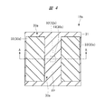
保持基板(基体)30の主面30aには、隔膜(膜部)19が形成された領域30c以外の領域に、緩衝膜(膜部)33からなるパターン33aが形成されている。緩衝膜33は、保持基板30の主面30aにおいて、隔膜19(薄膜31)よりも上方に、すなわち、Z軸方向(一次荷電粒子線が照射される方向)に沿って、隔膜19よりも試料12側に(試料ステージ22側に)位置するように、形成されている。緩衝膜33は、試料ステージ(保持部)22に保持されている試料12と隔膜19とが接触することを防止する。図3に示す例では、緩衝膜33は、主面30a上であって、薄膜31上に形成されている。
On the main surface 30a of the holding substrate (base body) 30, a pattern 33a made of a buffer film (film part) 33 is formed in a region other than the region 30c where the diaphragm (film part) 19 is formed. The buffer film 33 is higher than the diaphragm 19 (thin film 31) on the main surface 30a of the holding substrate 30, that is, along the Z-axis direction (the direction in which the primary charged particle beam is irradiated). It is formed so as to be located on the 12 side (on the sample stage 22 side). The buffer film 33 prevents the sample 12 held on the sample stage (holding unit) 22 and the diaphragm 19 from contacting each other. In the example shown in FIG. 3, the buffer film 33 is formed on the main surface 30 a and on the thin film 31.
例えば表面に凹凸を有し、最大高さが大きい試料12を保持した状態で、高倍率で焦点を合わせるために試料ステージ22をZ軸方向に移動させる場合、隔膜素子18aと試料12とが接触しやすい。しかし、本実施の形態1では、保持基板30の主面30aにおいて、Z軸方向(一次荷電粒子線が照射される方向)に沿って、隔膜19よりも試料12側に(試料ステージ22側に)位置するように、緩衝膜33が形成されている。そのため、隔膜素子18aと試料12とが接触するときは、緩衝膜33と試料12とが接触することで、隔膜19と試料12とが接触することを防止することができる。
For example, when the sample stage 22 is moved in the Z-axis direction for focusing at a high magnification while holding the sample 12 having an uneven surface and a maximum maximum height, the diaphragm element 18a and the sample 12 are in contact with each other. It's easy to do. However, in the first embodiment, the main surface 30a of the holding substrate 30 is closer to the sample 12 side (to the sample stage 22 side) than the diaphragm 19 along the Z-axis direction (direction in which the primary charged particle beam is irradiated). The buffer film 33 is formed so as to be positioned. Therefore, when the diaphragm element 18a and the sample 12 are in contact, the buffer film 33 and the sample 12 are in contact with each other, thereby preventing the diaphragm 19 and the sample 12 from being in contact with each other.
緩衝膜(膜部)33の膜厚は、試料12の厚さにもよるが、試料12の厚さが例えば20μmよりも薄いときは、膜厚の上限値を例えば20μmとし、膜厚の下限値を試料12の厚さとすることができる。例えば塗布法など比較的膜厚が大きな膜を形成するのに適した方法により緩衝膜33を形成する場合であっても、膜厚が20μmを超えると、保持基板30の主面30aの面内において、膜厚や膜質にむらが発生し、緩衝膜33の表面に凹凸が発生するおそれがある。
The film thickness of the buffer film (film part) 33 depends on the thickness of the sample 12, but when the thickness of the sample 12 is less than 20 μm, for example, the upper limit value of the film thickness is set to 20 μm, for example. The value can be the thickness of the sample 12. For example, even when the buffer film 33 is formed by a method suitable for forming a film having a relatively large film thickness such as a coating method, if the film thickness exceeds 20 μm, the in-plane of the main surface 30a of the holding substrate 30 In this case, the film thickness and the film quality may be uneven and the surface of the buffer film 33 may be uneven.
緩衝膜(膜部)33として、好適には、有機膜、無機膜または金属膜からなるものを用いることができる。これにより、観察される試料の厚さ、荷電粒子の種類、製造工程の制約等に応じて、最適な材料を選択することができる。また、緩衝膜33の材料として、有機膜を用いる場合には、例えばポリイミドを用いることができる。ポリイミドは、容易に形成することができ、耐熱性、安定性に優れる。したがって、緩衝膜33の材料としてポリイミドを用いることにより、耐熱性、安定性に優れた緩衝膜33を容易に製造することができる。
As the buffer film (film part) 33, an organic film, an inorganic film, or a metal film can be preferably used. Thereby, the optimal material can be selected according to the thickness of the sample to be observed, the kind of charged particles, restrictions on the manufacturing process, and the like. Further, when an organic film is used as the material of the buffer film 33, for example, polyimide can be used. Polyimide can be easily formed and has excellent heat resistance and stability. Therefore, by using polyimide as the material of the buffer film 33, the buffer film 33 having excellent heat resistance and stability can be easily manufactured.
緩衝膜(膜部)33からなるパターン33aは、平面視において、保持基板(基体)30の主面30aのうち、隔膜(膜部)19が形成された領域30cを挟んだ2つの領域に、形成されている。図4に示すように、例えば隔膜19の平面形状が正方形である場合、緩衝膜33からなるパターン33aは、好適には、隔膜19の外周の4辺のうち、少なくとも対向する2辺の外側の領域に形成されている。つまり、緩衝膜33からなるパターン33aは、好適には、平面視において、保持基板30の主面30aのうち、隔膜19が形成された領域30cを挟んで位置する少なくとも2つの領域30d、30eに形成されている。
The pattern 33a composed of the buffer film (film part) 33 is, in plan view, in two areas between the main surface 30a of the holding substrate (base body) 30 with the area 30c where the diaphragm (film part) 19 is formed. Is formed. As shown in FIG. 4, for example, when the planar shape of the diaphragm 19 is a square, the pattern 33 a made up of the buffer film 33 is preferably outside of at least two opposing sides of the four sides of the outer periphery of the diaphragm 19. Formed in the region. In other words, the pattern 33a formed of the buffer film 33 is preferably formed in at least two regions 30d and 30e located on the main surface 30a of the holding substrate 30 with the region 30c formed with the diaphragm 19 interposed therebetween in plan view. Is formed.
これにより、緩衝膜33と試料12とが接触した場合でも、保持基板30の主面30aに加えられる力を、平面視において、隔膜19が形成された領域30cを挟んで位置する2つの領域30d、30eに均等に分散させることができる。その結果、隔膜素子18aおよび試料12の一方が他方に対して傾斜することがなく、隔膜19と試料12とが接触することをさらに確実に防止することができる。
Thereby, even when the buffer film 33 and the sample 12 are in contact with each other, the force applied to the main surface 30a of the holding substrate 30 is two regions 30d positioned across the region 30c where the diaphragm 19 is formed in plan view. , 30e can be evenly distributed. As a result, one of the diaphragm element 18a and the sample 12 is not inclined with respect to the other, and the diaphragm 19 and the sample 12 can be more reliably prevented from contacting each other.
また、領域30dと領域30eとの間の領域、すなわち、緩衝膜33が除去された領域は、後述する実施の形態2において、隔膜素子18aと試料12との間に空気よりも軽いガスを供給する際に、供給されたガスが流れる流路FPとして機能する。この流路FPは、保持基板30の主面30a上で、平面視において、隔膜19が形成された領域30cを通り、一方の側から反対側まで横切るように、形成されていることが好ましい。これにより、隔膜素子18aと試料12との間に空気よりも軽いガスを供給する際に、供給されたガスを、隔膜19と試料12との間に確実に流すことができるので、荷電粒子線装置により得られる画像のS/N比を改善することができる。
Further, in the region between the region 30d and the region 30e, that is, the region where the buffer film 33 is removed, a gas lighter than air is supplied between the diaphragm element 18a and the sample 12 in the second embodiment to be described later. When it does, it functions as the flow path FP through which the supplied gas flows. The flow path FP is preferably formed on the main surface 30a of the holding substrate 30 so as to cross from the one side to the opposite side through the region 30c where the diaphragm 19 is formed in plan view. Accordingly, when a gas lighter than air is supplied between the diaphragm element 18a and the sample 12, the supplied gas can surely flow between the diaphragm 19 and the sample 12, so that the charged particle beam The S / N ratio of the image obtained by the apparatus can be improved.
なお、緩衝膜33からなるパターンが、隔膜19が形成された領域30cを挟んで位置する少なくとも2つの領域に形成されている場合とは、緩衝膜33が、隔膜19が形成された領域30cを挟んで位置する2つの領域を含む領域に形成されている場合も含まれる。したがって、緩衝膜33からなるパターンが、隔膜19が形成された領域30cを挟んで位置する2つの領域を含む領域に、一体として形成されている場合も含まれる。例えば図5を用いて後述するように、緩衝膜33からなるパターンが、平面視において、隔膜19が形成された領域30cの三方を囲むように、一体として形成されている場合も含まれる。あるいは、図6を用いて後述するように、緩衝膜33からなるパターンが、平面視において、隔膜19が形成された領域30cの四方を囲むように、一体として形成されている場合も含まれる。
In the case where the pattern formed of the buffer film 33 is formed in at least two regions located across the region 30c in which the diaphragm 19 is formed, the buffer film 33 defines the region 30c in which the diaphragm 19 is formed. The case where it is formed in a region including two regions located between each other is also included. Therefore, the case where the pattern which consists of the buffer film 33 is integrally formed in the area | region containing the 2 area | region located on both sides of the area | region 30c in which the diaphragm 19 was formed is also included. For example, as will be described later with reference to FIG. 5, the pattern including the buffer film 33 is integrally formed so as to surround three sides of the region 30 c where the diaphragm 19 is formed in a plan view. Alternatively, as will be described later with reference to FIG. 6, the case where the pattern formed of the buffer film 33 is integrally formed so as to surround the four sides of the region 30 c where the diaphragm 19 is formed in a plan view is also included.
緩衝膜(膜部)33からなるパターン33aは、平面視において、少なくとも主面30aにおける貫通孔32の開口32aの外周よりも周縁側に離れた領域に形成されている。すなわち、緩衝膜33からなるパターン33aは、少なくとも隔膜(膜部)19が形成された領域30cよりも周縁側に離れた領域に形成されている。これにより、緩衝膜33からなるパターン33aが、平面視において、開口32aすなわち隔膜19と重ならないようにすることができ、開口32aを覆うように形成された隔膜19の全ての部分で荷電粒子線を透過または通過させることができる。
The pattern 33a composed of the buffer film (film part) 33 is formed in a region farther from the outer periphery of the opening 32a of the through hole 32 in the main surface 30a than at the periphery in plan view. That is, the pattern 33a made of the buffer film 33 is formed in a region that is at least on the peripheral side of the region 30c where the diaphragm (film part) 19 is formed. Thereby, the pattern 33a made of the buffer film 33 can be prevented from overlapping the opening 32a, that is, the diaphragm 19 in a plan view, and the charged particle beam is applied to all portions of the diaphragm 19 formed so as to cover the opening 32a. Can be transmitted or passed.
また、緩衝膜(膜部)33からなるパターン33aは、平面視において、保持基板(基体)30の周縁よりも所定の幅寸法d3だけ隔膜(膜部)19側に(中央部側に)離れた領域に形成されている。これにより、隔膜素子18aの製造工程において、隔膜素子18aをダイシングして個片化する際に、緩衝膜33を、ダイシングされる領域(スクライブ領域)を位置合わせするための位置合わせマークとして、用いることができる。
Further, the pattern 33a formed of the buffer film (film part) 33 is separated from the peripheral edge of the holding substrate (base body) 30 by a predetermined width dimension d3 toward the diaphragm (film part) 19 side (to the center part side) in plan view. Formed in the region. Thus, in the manufacturing process of the diaphragm element 18a, when the diaphragm element 18a is diced into individual pieces, the buffer film 33 is used as an alignment mark for aligning a dicing area (scribe area). be able to.
したがって、緩衝膜(膜部)33からなるパターン33aは、平面視において、隔膜(膜部)19が形成された領域30cよりも周縁側に離れ、かつ、保持基板(基体)30の周縁よりも所定の幅寸法d3だけ中央部側に離れた領域30d、30eに形成されている。
Therefore, the pattern 33 a made up of the buffer film (film part) 33 is farther from the peripheral side than the region 30 c where the diaphragm (film part) 19 is formed in a plan view, and more than the peripheral edge of the holding substrate (base body) 30. It is formed in regions 30d and 30e that are separated by a predetermined width dimension d3 toward the center.
幅寸法d3の好適な範囲は、隔膜素子18aをダイシングする方法に依存する。ダイヤモンドの回転刃(ブレード)を備えたダイシング装置によりダイシングを行う場合、カット水の影響を考慮する必要があるため、幅寸法d3の好適な範囲は、例えば50~500μmである。また、レーザによりダイシングを行う場合、隔膜19が受ける損傷が少なく、隔膜素子18aの周縁すなわちダイシング面の平滑性を維持した状態で加工できるため、幅寸法d3については、ダイシング装置によりダイシングを行う場合に比べて小さくなる。レーザによりダイシングを行う場合、幅寸法d3の好適な範囲は、例えば1μm以上である。
The preferred range of the width dimension d3 depends on the method of dicing the diaphragm element 18a. When dicing is performed by a dicing apparatus equipped with a diamond rotating blade (blade), the influence of the cut water needs to be taken into consideration, and therefore the preferred range of the width dimension d3 is, for example, 50 to 500 μm. In addition, when dicing with a laser, the diaphragm 19 is less damaged and can be processed while maintaining the smoothness of the peripheral edge of the diaphragm element 18a, that is, the dicing surface. Therefore, for the width dimension d3, the dicing apparatus performs dicing. Smaller than When dicing with a laser, a suitable range of the width dimension d3 is, for example, 1 μm or more.
さらに好適には、図3に示すように、緩衝膜(膜部)33からなるパターン33aは、主面30bにおける薄膜31の開口部31aすなわち貫通孔32の外周よりも所定の幅寸法d4だけ周縁側に離れた領域に形成されている。これにより、緩衝膜33が、平面視において、開口部31aすなわち貫通孔32と重なる領域に形成されないようにすることができる。つまり、緩衝膜33が、保持基板30のうち、貫通孔32が形成されて厚さが薄くなった強度の小さい部分に形成されないようにすることができる。幅寸法d4については、例えば0~500μm程度とすることができる。
More preferably, as shown in FIG. 3, the pattern 33a formed of the buffer film (film part) 33 has a predetermined width dimension d4 rather than the opening 31a of the thin film 31 on the main surface 30b, that is, the outer periphery of the through hole 32. It is formed in a region away from the edge side. Thereby, it is possible to prevent the buffer film 33 from being formed in a region overlapping the opening 31a, that is, the through hole 32 in a plan view. In other words, the buffer film 33 can be prevented from being formed in the portion of the holding substrate 30 with a low strength where the through hole 32 is formed and the thickness is reduced. The width dimension d4 can be set to about 0 to 500 μm, for example.
なお、緩衝膜33からなるパターン33aが、開口部31aの外周よりも周縁側に離れた領域に形成されるのは、緩衝膜33が有する応力が隔膜19に影響を及ぼすおそれがある場合である。したがって、緩衝膜33が有する応力が極めて小さい場合には、緩衝膜33からなるパターン33aは、平面視において、隔膜19が形成された領域30cよりも周縁側に離れた領域であって、開口部31a内の部分にも形成することができる。この場合、緩衝膜33は、隔膜19が形成された領域30cよりも例えば1μm以上周縁側に離れた領域に形成することができる。
The pattern 33a formed of the buffer film 33 is formed in a region farther to the peripheral side than the outer periphery of the opening 31a when the stress of the buffer film 33 may affect the diaphragm 19. . Therefore, when the stress of the buffer film 33 is extremely small, the pattern 33a made of the buffer film 33 is a region farther to the peripheral side than the region 30c in which the diaphragm 19 is formed in plan view, and has an opening portion. It can also be formed in a portion within 31a. In this case, the buffer film 33 can be formed in a region separated from the region 30c in which the diaphragm 19 is formed by, for example, 1 μm or more on the peripheral side.
<隔膜素子の第1変形例~第3変形例>
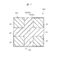
図5~図7は、それぞれ、実施の形態1の第1変形例~第3変形例の隔膜素子を試料側から見た平面図である。図5~図7は、それぞれ、平面視における緩衝膜33からなるパターンのパターン形状が異なる隔膜素子18b~18dを示す。
<First to third modified examples of diaphragm element>
5 to 7 are plan views of the diaphragm elements of the first to third modifications of the first embodiment as viewed from the sample side. 5 to 7 show diaphragm elements 18b to 18d having different pattern shapes of the buffer film 33 in plan view, respectively.
図5に示すように、実施の形態1の第1変形例の隔膜素子(隔膜部材)18bでは、隔膜(膜部)19の平面形状が正方形であり、緩衝膜(膜部)33からなるパターン33bが、平面視において、隔膜19の外周の4辺のうち3辺の外側の領域に形成されている。また、緩衝膜33からなるパターン33bが、平面視において、隔膜19が形成された領域30cの三方を囲むように、一体として形成されている。
As shown in FIG. 5, in the diaphragm element (diaphragm member) 18 b of the first modification of the first embodiment, the planar shape of the diaphragm (film part) 19 is a square, and the pattern is formed of the buffer film (film part) 33. 33b is formed in the area | region of the outer side of 3 sides among 4 sides of the outer periphery of the diaphragm 19 in planar view. Further, the pattern 33b made of the buffer film 33 is integrally formed so as to surround three sides of the region 30c in which the diaphragm 19 is formed in a plan view.
図5に示す隔膜素子18bにおいて、隔膜19の外周の4辺のうち、その外側に緩衝膜33が形成された辺の数は、3つであり、図4に示す隔膜素子18aにおいて、その外側に緩衝膜33が形成された辺の数(2つ)よりも多い。そのため、隔膜素子18bは、表面に凹凸を有する試料12を移動する際に、隔膜19と試料12とが接触することを、隔膜素子18aよりも確実に防止することができる。
In the diaphragm element 18b shown in FIG. 5, the number of sides on which the buffer film 33 is formed outside the four sides of the outer periphery of the diaphragm 19 is three. In the diaphragm element 18a shown in FIG. More than the number of sides (two) on which the buffer film 33 is formed. Therefore, the diaphragm element 18b can prevent the diaphragm 19 and the sample 12 from contacting each other more reliably than the diaphragm element 18a when moving the sample 12 having an uneven surface.
図6に示すように、実施の形態1の第2変形例の隔膜素子(隔膜部材)18cでは、隔膜(膜部)19の平面形状が正方形であり、緩衝膜(膜部)33からなるパターン33cが、平面視において、隔膜19の外周の4辺全ての外側の領域に形成されている。また、緩衝膜33からなるパターン33cが、平面視において、隔膜19が形成された領域30cの四方を囲むように、一体として形成されている。
As shown in FIG. 6, in the diaphragm element (diaphragm member) 18 c of the second modification of the first embodiment, the planar shape of the diaphragm (film part) 19 is a square, and the pattern is composed of the buffer film (film part) 33. 33c is formed in the area | region of the outer side of all four sides of the outer periphery of the diaphragm 19 in planar view. Further, the pattern 33c made of the buffer film 33 is integrally formed so as to surround the four sides of the region 30c in which the diaphragm 19 is formed in a plan view.
図6に示す隔膜素子18cにおいて、隔膜19の外周の4辺のうち、その外側に緩衝膜33が形成された辺の数は、4つであり、図5に示す隔膜素子18bにおいて、その外側に緩衝膜33が形成された辺の数(3つ)よりも多い。そのため、隔膜素子18cは、表面に凹凸を有する試料12を移動する際に、隔膜19と試料12とが接触することを、隔膜素子18bよりもさらに確実に防止することができる。
In the diaphragm element 18c shown in FIG. 6, the number of sides on which the buffer film 33 is formed outside the four sides of the outer periphery of the diaphragm 19 is four. In the diaphragm element 18b shown in FIG. More than the number of sides (three) on which the buffer film 33 is formed. Therefore, the diaphragm element 18c can prevent the diaphragm 19 and the sample 12 from contacting each other more reliably than the diaphragm element 18b when moving the sample 12 having an uneven surface.
図7に示すように、実施の形態1の第3変形例の隔膜素子(隔膜部材)18dでは、隔膜19の平面形状が正方形であり、緩衝膜(膜部)33からなるパターン33dが、隔膜19の各頂点よりも対角線方向に沿って外側に、4箇所に分離して形成されている。また、隔膜19の外周の4辺のうちいずれの辺の外側の領域にも、緩衝膜33が形成されていない。すなわち、隔膜19が形成された領域30cで交差する十字形状の領域において、緩衝膜33が除去されている。
As shown in FIG. 7, in the diaphragm element (diaphragm member) 18d of the third modification of the first embodiment, the planar shape of the diaphragm 19 is square, and the pattern 33d made of the buffer film (film part) 33 is formed as a diaphragm. It is divided into four locations on the outer side along the diagonal direction with respect to 19 vertices. In addition, the buffer film 33 is not formed in a region outside any of the four sides on the outer periphery of the diaphragm 19. That is, the buffer film 33 is removed in a cross-shaped region intersecting with the region 30c where the diaphragm 19 is formed.
このような、緩衝膜33が除去された十字形状の領域は、後述する実施の形態2において、隔膜素子18dと試料12との間に空気よりも軽いガスを供給する際に、供給されたガスが流れる流路FPとして機能する。この流路FPは、主面30a上で、平面視において、隔膜19が形成された領域30cを通り、一方の側から反対側まで横切るように形成された、互いに交差する2つの流路からなることが好ましい。これにより、隔膜素子18dと試料12との間に空気よりも軽いガスを供給する際に、供給されたガスを、隔膜19と試料12との間に確実に流すことができるので、荷電粒子線装置により得られる画像のS/N比を改善することができる。
Such a cross-shaped region from which the buffer film 33 is removed is the gas supplied when a gas lighter than air is supplied between the diaphragm element 18d and the sample 12 in the second embodiment to be described later. Functions as a flow path FP through which. This flow path FP is composed of two flow paths that intersect each other and are formed so as to cross from the one side to the opposite side through the region 30c in which the diaphragm 19 is formed on the main surface 30a in plan view. It is preferable. Thus, when a gas lighter than air is supplied between the diaphragm element 18d and the sample 12, the supplied gas can surely flow between the diaphragm 19 and the sample 12, so that the charged particle beam The S / N ratio of the image obtained by the apparatus can be improved.
<隔膜素子の製造工程>
次に、本実施の形態1の隔膜素子(隔膜部材)の製造工程の一例を説明する。
<Manufacturing process of diaphragm element>
Next, an example of the manufacturing process of the diaphragm element (diaphragm member) according to the first embodiment will be described.
図8~図14は、実施の形態1の隔膜素子の製造工程中の要部断面図である。なお、図8~図14は、上記図3に対応する断面を示す。
8 to 14 are cross-sectional views of a main part during the manufacturing process of the diaphragm element according to the first embodiment. 8 to 14 show cross sections corresponding to FIG.
まず、図8に示すように、主面30a、および、主面30aと反対側の主面30bを有する保持基板(基体)30を用意する。前述したように、保持基板30として、例えば基板方位(100)または(110)のSi基板を用いることができる。これにより、後述するように、アルカリ性水溶液からなるエッチング液を用いた異方性エッチングを行うことで、保持基板30に貫通孔32(図3参照)を容易に形成することができる。また、保持基板30として、両面が鏡面に仕上げられた基板を用いることができる。これにより、保持基板30の両面に、容易に加工を施すことができる。
First, as shown in FIG. 8, a holding substrate (base body) 30 having a main surface 30a and a main surface 30b opposite to the main surface 30a is prepared. As described above, for example, a Si substrate having a substrate orientation (100) or (110) can be used as the holding substrate 30. Thereby, as will be described later, through-holes 32 (see FIG. 3) can be easily formed in the holding substrate 30 by performing anisotropic etching using an etching solution made of an alkaline aqueous solution. Further, as the holding substrate 30, a substrate whose both surfaces are mirror-finished can be used. Thereby, it is possible to easily process both surfaces of the holding substrate 30.
なお、図8では、保持基板30のうち1つの隔膜素子が形成される領域のみを図示するが、実際には、保持基板30は、主面30aまたは主面30bに平行な方向に沿って、複数の隔膜素子が形成される領域を含むものである(図9~図14においても同様)。
In FIG. 8, only the region where one diaphragm element is formed in the holding substrate 30 is illustrated, but actually, the holding substrate 30 is along a direction parallel to the main surface 30a or the main surface 30b. This includes a region where a plurality of diaphragm elements are formed (the same applies to FIGS. 9 to 14).
次に、図9に示すように、保持基板(基体)30の両面、すなわち主面30aおよび主面30bに、薄膜31を形成する。例えば700℃の温度で、化学的気相成長(Chemical Vapor Deposition:CVD)法により、薄膜31として、SiN膜を形成することができる。
Next, as shown in FIG. 9, the thin film 31 is formed on both surfaces of the holding substrate (base body) 30, that is, the main surface 30a and the main surface 30b. For example, a SiN film can be formed as the thin film 31 at a temperature of 700 ° C. by a chemical vapor deposition (CVD) method.
なお、前述したように、薄膜31の厚さは、好適には、例えば5~50nmであり、さらに好適には、例えば5~20nmである。また、前述したように、薄膜31として、引っ張り応力を有する膜が好ましく、例えばSiN、AlNなどの金属の窒化物、または、ポリイミドからなることが好ましい。
As described above, the thickness of the thin film 31 is preferably, for example, 5 to 50 nm, and more preferably, for example, 5 to 20 nm. Further, as described above, the thin film 31 is preferably a film having tensile stress, and is preferably made of a metal nitride such as SiN or AlN, or polyimide.
また、後述する工程により形成される隔膜(メンブレン、膜部)19の耐圧力性を向上するため、薄膜31を形成した後、薄膜31を形成した時の温度以上の温度で熱処理を行うことが好ましい。このような熱処理により、隔膜19が焼結されて密度が増加し、剛性が向上するため、隔膜19の耐圧力性が向上する。例えば薄膜31がSiNからなる場合は、熱処理の温度は、好適には、800℃以上である。
Moreover, in order to improve the pressure resistance of the diaphragm (membrane, film part) 19 formed by the process described later, after the thin film 31 is formed, heat treatment is performed at a temperature equal to or higher than the temperature at which the thin film 31 is formed. preferable. By such heat treatment, the diaphragm 19 is sintered to increase the density and improve the rigidity, so that the pressure resistance of the diaphragm 19 is improved. For example, when the thin film 31 is made of SiN, the heat treatment temperature is preferably 800 ° C. or higher.
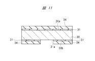
次に、図10に示すように、両面に薄膜31が形成された保持基板(基体)30の両面、すなわち主面30aおよび主面30bに、絶縁膜34を形成する。絶縁膜34を形成することで、後述する工程により隔膜19を形成するまでの間、薄膜31を保護することができ、薄膜31に傷が付くことを防止または抑制することができる。例えばCVD法により、絶縁膜34として、酸化シリコン(SiO2)膜を形成することができる。
Next, as shown in FIG. 10, the insulating film 34 is formed on both surfaces of the holding substrate (base) 30 having the thin film 31 formed on both surfaces, that is, the main surface 30a and the main surface 30b. By forming the insulating film 34, the thin film 31 can be protected until the diaphragm 19 is formed by a process described later, and the thin film 31 can be prevented or suppressed from being damaged. For example, a silicon oxide (SiO 2 ) film can be formed as the insulating film 34 by CVD.
このとき、絶縁膜34を、保持基板30の両面のうち、隔膜19が形成される主面30aのみに形成することもできる。しかしながら、好適には、図10に示すように、保持基板30の主面30aおよび主面30bの両面に、絶縁膜34を形成する。主面30aのみならず主面30bにも絶縁膜34を形成することで、主面30bにおいて保持基板30をエッチングにより除去する際のマスクとなる薄膜31に傷が付くことを、防止または抑制することができる。
At this time, the insulating film 34 can be formed only on the main surface 30 a on which the diaphragm 19 is formed, on both surfaces of the holding substrate 30. However, preferably, as shown in FIG. 10, insulating films 34 are formed on both the main surface 30 a and the main surface 30 b of the holding substrate 30. By forming the insulating film 34 not only on the main surface 30a but also on the main surface 30b, the thin film 31 that serves as a mask when the holding substrate 30 is removed by etching on the main surface 30b is prevented or suppressed. be able to.
次に、図11に示すように、保持基板(基体)30の主面30bにおいて、絶縁膜34および薄膜31に開口部31aを形成する。保持基板30の主面30bであって貫通孔32(図3参照)を形成する領域において、例えばフォトリソグラフィー技術およびエッチングにより絶縁膜34と薄膜31を除去する。これにより、絶縁膜34および薄膜31を貫通して保持基板30に到達する開口部31aを形成する。開口部31aでは、保持基板30が露出する。
Next, as shown in FIG. 11, openings 31 a are formed in the insulating film 34 and the thin film 31 on the main surface 30 b of the holding substrate (base body) 30. In the region where the through hole 32 (see FIG. 3) is formed on the main surface 30b of the holding substrate 30, the insulating film 34 and the thin film 31 are removed by, for example, photolithography and etching. Thereby, an opening 31 a that penetrates the insulating film 34 and the thin film 31 and reaches the holding substrate 30 is formed. In the opening 31a, the holding substrate 30 is exposed.
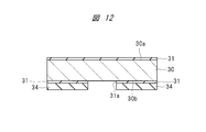
次に、図12に示すように、保持基板(基体)30の主面30aにおいて、絶縁膜34を除去する。これにより、保持基板30の主面30aでは、薄膜31が表面に露出する。
Next, as shown in FIG. 12, the insulating film 34 is removed from the main surface 30 a of the holding substrate (base body) 30. As a result, the thin film 31 is exposed on the main surface 30 a of the holding substrate 30.
次に、図13に示すように、保持基板(基体)30の主面30aにおいて、緩衝膜(膜部)33を形成する。前述したように、緩衝膜33として、有機膜、無機膜または金属膜からなるものを形成することができ、有機膜の材料としては、例えばポリイミドを用いることができる。また、緩衝膜33の膜厚は、試料12の厚さにもよるが、試料12の厚さが例えば20μmよりも薄いときは、膜厚の上限値を例えば20μmとし、膜厚の下限値を試料の厚さとすることができる。
Next, as shown in FIG. 13, a buffer film (film part) 33 is formed on the main surface 30 a of the holding substrate (base body) 30. As described above, the buffer film 33 can be formed of an organic film, an inorganic film, or a metal film. As the material of the organic film, for example, polyimide can be used. The film thickness of the buffer film 33 depends on the thickness of the sample 12, but when the thickness of the sample 12 is less than 20 μm, for example, the upper limit value of the film thickness is set to 20 μm and the lower limit value of the film thickness is set to, for example. It can be the thickness of the sample.
次に、図14に示すように、フォトリソグラフィー技術およびエッチングにより、緩衝膜(膜部)33の一部を除去し、緩衝膜33からなるパターン33aを形成する。
Next, as shown in FIG. 14, a part of the buffer film (film part) 33 is removed by a photolithography technique and etching, and a pattern 33a made of the buffer film 33 is formed.
緩衝膜33からなるパターン33aを、平面視において、保持基板(基体)30の周縁よりも所定の幅寸法d3だけ隔膜19側に(中央部側に)離れた領域に形成する。これにより、後の工程で、隔膜素子18aをダイシングして個片化する際に、緩衝膜33を、スクライブ領域を位置合わせするための位置合わせマークとして、用いることができる。
The pattern 33a made of the buffer film 33 is formed in a region separated from the peripheral edge of the holding substrate (base body) 30 by a predetermined width dimension d3 on the side of the diaphragm 19 (on the center side) in plan view. Thereby, when the diaphragm element 18a is diced and separated into individual pieces in a later step, the buffer film 33 can be used as an alignment mark for aligning the scribe region.
さらに、緩衝膜33からなるパターン33aを、開口部31aの外周よりも所定の幅寸法d4だけ周縁側に離れた領域に形成する。これにより、緩衝膜33が、平面視において、開口部31aすなわち貫通孔32と重なる領域に形成されないようにすることができる。つまり、緩衝膜33が、保持基板30のうち、貫通孔32が形成されて厚さが薄くなった強度の小さい部分に形成されないようにすることができる。幅寸法d4については、例えば0~500μm程度とすることができる。
Furthermore, the pattern 33a made of the buffer film 33 is formed in a region separated from the outer periphery of the opening 31a by a predetermined width dimension d4 toward the peripheral side. Thereby, it is possible to prevent the buffer film 33 from being formed in a region overlapping the opening 31a, that is, the through hole 32 in a plan view. In other words, the buffer film 33 can be prevented from being formed in the portion of the holding substrate 30 with a low strength where the through hole 32 is formed and the thickness is reduced. The width dimension d4 can be set to about 0 to 500 μm, for example.
なお、パターン33aを形成した後、樹脂膜(図示は省略)を塗布し、保持基板30の全面を覆うこともできる。
In addition, after forming the pattern 33a, a resin film (not shown) can be applied to cover the entire surface of the holding substrate 30.
次に、保持基板(基体)30に貫通孔32(図3参照)を形成する。保持基板30の主面30bにおいて、開口部31aが形成された薄膜31をマスクとして、アルカリ性水溶液からなるエッチング液を用いた異方性エッチングを行い、開口部31aに露出した保持基板30を除去する(エッチングする)。これにより、保持基板30に主面30bから主面30aに到達する貫通孔32(図3参照)を形成する。
Next, a through hole 32 (see FIG. 3) is formed in the holding substrate (base body) 30. On the main surface 30b of the holding substrate 30, anisotropic etching using an etching solution made of an alkaline aqueous solution is performed using the thin film 31 with the opening 31a formed as a mask to remove the holding substrate 30 exposed to the opening 31a. (Etching). Thus, a through hole 32 (see FIG. 3) that reaches the main surface 30a from the main surface 30b is formed in the holding substrate 30.
保持基板30として例えばSi基板を用いる場合、例えば水酸化カリウム(KOH)水溶液または水酸化テトラメチルアンモニウム(Tetra-methyl-ammonium-hydroxide:TMAH)水溶液などのアルカリ性水溶液からなるエッチング液を用いる。
For example, when a Si substrate is used as the holding substrate 30, an etching solution made of an alkaline aqueous solution such as an aqueous potassium hydroxide (KOH) solution or an aqueous tetramethylammonium hydroxide (TMAH) solution is used.
このようにして保持基板30に主面30bから主面30aに到達する貫通孔32(図3参照)を形成することで、主面30aにおいて貫通孔32の開口32a(図3参照)を覆うように残された薄膜31からなる隔膜19が形成される。その後、保持基板30をスクライブ領域でダイシングして個片化することで、図3に示したような隔膜素子18aが形成される。なお、後述するアタッチメントへの隔膜素子18aの装着において、保持基板30が厚い場合は、ダイシング前に主面30b面をバックグラインド法などにより薄くして高さ調整してもよい。その場合、主面30b面は保持基板30が露出した構造となる。
Thus, by forming the through hole 32 (see FIG. 3) reaching the main surface 30a from the main surface 30b in the holding substrate 30, the main surface 30a covers the opening 32a (see FIG. 3) of the through hole 32. A diaphragm 19 composed of the thin film 31 left on the film is formed. Thereafter, the holding substrate 30 is diced in the scribe region to be separated into individual pieces, whereby the diaphragm element 18a as shown in FIG. 3 is formed. In mounting the diaphragm element 18a on the attachment described later, when the holding substrate 30 is thick, the height of the main surface 30b may be adjusted by a back grinding method or the like before dicing. In that case, the main surface 30b has a structure in which the holding substrate 30 is exposed.
また、樹脂膜(図示は省略)により保持基板30の全面が覆われているときは、隔膜19および緩衝膜33上にある樹脂膜(図示は省略)を除去する。
Also, when the entire surface of the holding substrate 30 is covered with a resin film (not shown), the resin film (not shown) on the diaphragm 19 and the buffer film 33 is removed.
なお、貫通孔32(図3参照)を形成する前に、図14に示すように主面30bに絶縁膜34が形成されていたときは、貫通孔32を形成する前または貫通孔32を形成した後に、例えばフッ酸(HF)などのエッチング液により、絶縁膜34を除去する。
Before forming the through hole 32 (see FIG. 3), when the insulating film 34 is formed on the main surface 30b as shown in FIG. 14, before the through hole 32 is formed or the through hole 32 is formed. After that, the insulating film 34 is removed with an etchant such as hydrofluoric acid (HF).
保持基板(基体)30として基板方位が(100)または(110)であるSi基板を用い、異方性エッチングを行う場合、形成される貫通孔32の側面が(111)面になるため、貫通孔32を形状精度よく形成することができる。
When a Si substrate with a substrate orientation of (100) or (110) is used as the holding substrate (base body) 30 and anisotropic etching is performed, the side surface of the through-hole 32 to be formed becomes the (111) surface, so The hole 32 can be formed with high shape accuracy.
前述したように、保持基板30として基板方位が(100)であるSi基板を用いるときは、保持基板30の主面30a(または主面30b)に対して貫通孔32の側面がなす角が54~55°となる。そのため、隔膜(膜部)19すなわち貫通孔32の開口32aの幅寸法d1(図3参照)については、主面30bにおいて薄膜31に形成された開口部31a、すなわち貫通孔32の幅寸法d2よりも小さくなる。つまり、貫通孔32の幅寸法d2は、隔膜19の幅寸法d1よりも大きくなる。
As described above, when the Si substrate having the substrate orientation (100) is used as the holding substrate 30, the angle formed by the side surface of the through hole 32 with respect to the main surface 30a (or main surface 30b) of the holding substrate 30 is 54. ~ 55 °. Therefore, the width dimension d1 (see FIG. 3) of the diaphragm (film part) 19, that is, the opening 32a of the through hole 32, is larger than the opening 31a formed in the thin film 31 on the main surface 30b, that is, the width dimension d2 of the through hole 32. Becomes smaller. That is, the width dimension d2 of the through hole 32 is larger than the width dimension d1 of the diaphragm 19.
一方、保持基板30として基板方位が(110)であるSi基板を用いるときは、保持基板30の主面30a(または主面30b)に対して貫通孔32の側面がなす角が90°となる。そのため、貫通孔32の幅寸法d2が、隔膜(膜部)19の幅寸法d1と等しくなるので、隔膜素子18aを小型化することができる。
On the other hand, when a Si substrate with a substrate orientation of (110) is used as the holding substrate 30, the angle formed by the side surface of the through hole 32 with respect to the main surface 30a (or main surface 30b) of the holding substrate 30 is 90 °. . Therefore, since the width dimension d2 of the through hole 32 is equal to the width dimension d1 of the diaphragm (film part) 19, the diaphragm element 18a can be reduced in size.
なお、緩衝膜(膜部)33からなるパターン33aが、開口部31aの外周よりも周縁側に離れた領域に形成されるのは、緩衝膜33が有する応力が隔膜19に影響を及ぼすおそれがある場合である。したがって、緩衝膜33が有する応力が極めて小さい場合には、前述したように、緩衝膜33からなるパターン33aは、平面視において、隔膜19が形成された領域30c(図4参照)よりも周縁側に離れた領域であって、開口部31a内の部分にも形成することができる。この場合、緩衝膜33は、隔膜19が形成された領域30cよりも例えば1μm以上周縁側に離れた領域に形成することができる。
The pattern 33a formed of the buffer film (film part) 33 is formed in a region farther to the peripheral side than the outer periphery of the opening 31a because the stress of the buffer film 33 may affect the diaphragm 19. It is the case. Therefore, when the stress of the buffer film 33 is extremely small, as described above, the pattern 33a made of the buffer film 33 is more peripheral than the region 30c (see FIG. 4) where the diaphragm 19 is formed in plan view. It can also be formed in a portion in the opening portion 31a. In this case, the buffer film 33 can be formed in a region separated from the region 30c in which the diaphragm 19 is formed by, for example, 1 μm or more on the peripheral side.
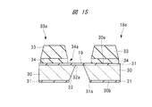
<隔膜素子の第4変形例>
図15は、実施の形態1の第4変形例の隔膜素子を示す要部断面図である。
<Fourth Modification of Diaphragm Element>
FIG. 15 is a cross-sectional view of relevant parts showing a diaphragm element according to a fourth modification of the first embodiment.
図3に示したように、実施の形態1の隔膜素子18aでは、保持基板30の主面30aにおいて、緩衝膜33は、薄膜31上に直接形成されている。一方、図15に示すように、実施の形態1の第4変形例の隔膜素子(隔膜部材)18eでは、保持基板(基体)30の主面30aにおいて、緩衝膜(膜部)33は、薄膜31上に、絶縁膜34を介して形成されている。すなわち、緩衝膜33からなるパターン33aは、薄膜31上に、絶縁膜34からなるパターン34aを介して形成されている。絶縁膜34からなるパターン34aは、平面視において、緩衝膜33からなるパターン33aと同一のパターンである。
As shown in FIG. 3, in the diaphragm element 18 a of the first embodiment, the buffer film 33 is directly formed on the thin film 31 on the main surface 30 a of the holding substrate 30. On the other hand, as shown in FIG. 15, in the diaphragm element (diaphragm member) 18 e of the fourth modification of the first embodiment, the buffer film (film part) 33 is a thin film on the main surface 30 a of the holding substrate (substrate) 30. An insulating film 34 is formed on 31. That is, the pattern 33 a made of the buffer film 33 is formed on the thin film 31 via the pattern 34 a made of the insulating film 34. The pattern 34a made of the insulating film 34 is the same pattern as the pattern 33a made of the buffer film 33 in plan view.
例えばポリイミドなどの有機膜、無機膜または金属膜からなる緩衝膜33が、例えばSiNからなる薄膜31上に直接形成された場合、緩衝膜33と薄膜31との間の接着性(密着力)が弱い場合がある。一方、例えばポリイミドなどの有機膜、無機膜または金属膜からなる緩衝膜33が、例えばSiNからなる薄膜31上に、例えばSiO2などからなる絶縁膜34を介して形成された場合、緩衝膜33と薄膜31との間の接着性(密着力)を向上させることができる。
For example, when the buffer film 33 made of an organic film such as polyimide, an inorganic film, or a metal film is directly formed on the thin film 31 made of, for example, SiN, the adhesiveness (adhesive force) between the buffer film 33 and the thin film 31 is improved. May be weak. On the other hand, when the buffer film 33 made of an organic film such as polyimide, an inorganic film, or a metal film is formed on the thin film 31 made of, for example, SiN via the insulating film 34 made of, for example, SiO 2 , the buffer film 33 is formed. It is possible to improve the adhesion (adhesion) between the thin film 31 and the thin film 31.
実施の形態1の隔膜素子18aの製造工程では、図11に示したように開口部31aを形成した後、図12に示したように、保持基板30の主面30aで絶縁膜34を除去する。
In the manufacturing process of the diaphragm element 18a according to the first embodiment, after forming the opening 31a as shown in FIG. 11, the insulating film 34 is removed on the main surface 30a of the holding substrate 30 as shown in FIG. .
一方、実施の形態1の第4変形例の隔膜素子18eの製造工程では、図11に示したように開口部31aを形成した後、保持基板30の主面30aで絶縁膜34を除去せずに、保持基板30の主面30aに緩衝膜33を形成する。そして、フォトリソグラフィー技術およびエッチングにより、緩衝膜33の一部を除去し、緩衝膜33からなるパターン33aを形成した後、パターン33aが形成されていない領域で、絶縁膜34を除去し、絶縁膜34からなるパターン34aを形成する。
On the other hand, in the manufacturing process of the diaphragm element 18e according to the fourth modification of the first embodiment, the insulating film 34 is not removed on the main surface 30a of the holding substrate 30 after the opening 31a is formed as shown in FIG. In addition, the buffer film 33 is formed on the main surface 30 a of the holding substrate 30. Then, a part of the buffer film 33 is removed by photolithography technique and etching to form a pattern 33a composed of the buffer film 33, and then the insulating film 34 is removed in a region where the pattern 33a is not formed. A pattern 34 a composed of 34 is formed.
その後は、実施の形態1の隔膜素子18aの製造工程と同様に、例えば樹脂膜(図示は省略)を形成し、異方性エッチングにより、開口部31aに露出した保持基板30を除去し(エッチングし)、貫通孔32を形成する。これにより、図15に示した隔膜素子18eが形成される。
After that, as in the manufacturing process of the diaphragm element 18a of the first embodiment, for example, a resin film (not shown) is formed, and the holding substrate 30 exposed to the opening 31a is removed by anisotropic etching (etching). A through hole 32 is formed. Thereby, the diaphragm element 18e shown in FIG. 15 is formed.
<隔膜素子の第5変形例>
図16は、実施の形態1の第5変形例の隔膜素子を示す要部断面図である。
<Fifth Modification of Diaphragm Element>
FIG. 16 is a cross-sectional view of relevant parts showing a diaphragm element according to a fifth modification of the first embodiment.
図15に示したように、実施の形態1の第4変形例の隔膜素子18eでは、絶縁膜34からなるパターン34aは、平面視において、緩衝膜33からなるパターン33aと同一のパターンである。
As shown in FIG. 15, in the diaphragm element 18e of the fourth modified example of the first embodiment, the pattern 34a made of the insulating film 34 is the same pattern as the pattern 33a made of the buffer film 33 in plan view.
一方、実施の形態1の第5変形例の隔膜素子(隔膜部材)18fでは、図16に示すように、絶縁膜34からなるパターン34bは、緩衝膜33からなるパターン33aが形成された領域より幅寸法d5だけ隔膜19側の(中央部側の)領域まで形成されている。なお、上記したパターン34bが形成されている領域は、隔膜(膜部)19が形成された領域30c(図4参照)よりも周縁側に離れ、かつ、保持基板(基体)30の周縁よりも中央部側に離れた領域に含まれている。
On the other hand, in the diaphragm element (diaphragm member) 18f of the fifth modification of the first embodiment, as shown in FIG. 16, the pattern 34b made of the insulating film 34 is more than the region where the pattern 33a made of the buffer film 33 is formed. It is formed up to the region on the side of the diaphragm 19 (center side) by the width dimension d5. Note that the region where the pattern 34 b is formed is farther from the periphery than the region 30 c (see FIG. 4) where the diaphragm (film part) 19 is formed, and more than the periphery of the holding substrate (base body) 30. It is included in the area away from the center.
このような構造により、実施の形態1の第4変形例の隔膜素子18eよりも、絶縁膜34が形成される領域が、隔膜19側に(中央部側に)拡張される。そして、緩衝膜33に加え、拡張された領域に形成された絶縁膜34も、隔膜19と試料12とが接触することを防止する。したがって、隔膜素子18fは、隔膜素子18eに比べ、隔膜19と試料12とが接触することを防止する機能をさらに強化することができる。
With this structure, the region where the insulating film 34 is formed is expanded toward the diaphragm 19 (to the center) than the diaphragm element 18e according to the fourth modification of the first embodiment. In addition to the buffer film 33, the insulating film 34 formed in the expanded region also prevents the diaphragm 19 and the sample 12 from contacting each other. Therefore, the diaphragm element 18f can further enhance the function of preventing the diaphragm 19 and the sample 12 from coming into contact with each other compared to the diaphragm element 18e.
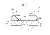
<隔膜素子の第6変形例>
図17は、実施の形態1の第6変形例の隔膜素子を示す要部断面図である。
<Sixth Modification of Diaphragm Element>
FIG. 17 is a main part sectional view showing a diaphragm element according to a sixth modification of the first embodiment.
図17に示すように、実施の形態1の第6変形例の隔膜素子(隔膜部材)18gは、実施の形態1の隔膜素子(隔膜部材)18aにおいて、緩衝膜(膜部)33からなるパターン33a上に、導電膜からなるシール膜(膜部)35が形成されたものである。すなわち、導電膜からなるシール膜35は、緩衝膜33からなるパターン33aの表面に形成されている。このような構造により、試料12から放出された二次荷電粒子が緩衝膜33または隔膜19に蓄積されることを防止することができ、検出器13により二次荷電粒子が検出される感度が低下することを防止することができる。つまり、緩衝膜33または隔膜19に二次荷電粒子が蓄積されることによる感度低下を防止することができる。
As shown in FIG. 17, the diaphragm element (diaphragm member) 18 g of the sixth modification of the first embodiment is a pattern comprising the buffer film (film part) 33 in the diaphragm element (diaphragm member) 18 a of the first embodiment. A sealing film (film part) 35 made of a conductive film is formed on 33a. That is, the seal film 35 made of a conductive film is formed on the surface of the pattern 33 a made of the buffer film 33. With such a structure, it is possible to prevent the secondary charged particles emitted from the sample 12 from being accumulated in the buffer film 33 or the diaphragm 19, and the sensitivity of detecting the secondary charged particles by the detector 13 is lowered. Can be prevented. That is, it is possible to prevent a decrease in sensitivity due to accumulation of secondary charged particles in the buffer film 33 or the diaphragm 19.
また、シール膜35は、保持基板(基体)30の側面30fにも形成されていてもよい。すなわち、シール膜35は、緩衝膜33からなるパターン33aの表面、および保持基板30の側面30fに、一体として形成されている。これにより、後述する実施の形態2で説明するように、緩衝膜33または隔膜19に二次荷電粒子が蓄積されることによる感度低下をさらに防止することができる。また、側面30fにシール膜35が形成されていない場合は、筐体3とシール膜35が導通するように銀ペーストまたは導電シールなどを用いて、緩衝膜33や隔膜19に二次荷電粒子が蓄積することを防止する。
The sealing film 35 may also be formed on the side surface 30 f of the holding substrate (base body) 30. That is, the seal film 35 is integrally formed on the surface of the pattern 33 a made of the buffer film 33 and the side surface 30 f of the holding substrate 30. Thereby, as will be described in the second embodiment to be described later, it is possible to further prevent a decrease in sensitivity due to accumulation of secondary charged particles in the buffer film 33 or the diaphragm 19. Further, when the seal film 35 is not formed on the side surface 30f, secondary charged particles are formed on the buffer film 33 and the diaphragm 19 by using silver paste or a conductive seal so that the housing 3 and the seal film 35 are electrically connected. Prevent accumulation.
シール膜35として、アルミニウム(Al)、銅(Cu)、タングステン(W)、チタン(Ti)、タンタル(Ta)、クロム(Cr)、ニッケル(Ni)、またはモリブデン(Mo)などの金属からなる導電膜を用いることができる。あるいは、シール膜35として、窒化タングステン(WN)、もしくは窒化チタン(TiN)などの金属窒化物、または珪化タングステン(WSi)、もしくは珪化ニッケル(NiSi)などの金属化合物からなる導電膜を用いることができる。
The seal film 35 is made of a metal such as aluminum (Al), copper (Cu), tungsten (W), titanium (Ti), tantalum (Ta), chromium (Cr), nickel (Ni), or molybdenum (Mo). A conductive film can be used. Alternatively, a conductive film made of a metal nitride such as tungsten nitride (WN) or titanium nitride (TiN) or a metal compound such as tungsten silicide (WSi) or nickel silicide (NiSi) is used as the seal film 35. it can.
実施の形態1の第6変形例の隔膜素子18gの製造工程では、実施の形態1の隔膜素子18aを製造した後、隔膜19をマスクするように遮蔽板を配置した状態で、例えばスパッタ法または蒸着法により、導電膜からなるシール膜35を形成する。
In the manufacturing process of the diaphragm element 18g according to the sixth modification of the first embodiment, after manufacturing the diaphragm element 18a according to the first embodiment, a shielding plate is disposed so as to mask the diaphragm 19, A seal film 35 made of a conductive film is formed by vapor deposition.
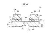
<隔膜素子の第7変形例>
図18は、実施の形態1の第7変形例の隔膜素子を示す要部断面図である。
<Seventh Modification of Diaphragm Element>
FIG. 18 is a cross-sectional view of relevant parts showing a diaphragm element according to a seventh modification of the first embodiment.
図18に示すように、実施の形態1の第7変形例の隔膜素子(隔膜部材)18hは、実施の形態1の第4変形例の隔膜素子(隔膜部材)18eにおいて、緩衝膜(膜部)33からなるパターン33a上に、導電膜からなるシール膜(膜部)35が形成されたものである。すなわち、導電膜からなるシール膜35は、緩衝膜33からなるパターン33aの表面に形成されている。このような構造により、実施の形態1の第4変形例の隔膜素子18eと同様に、緩衝膜33と薄膜31との間の接着性(密着力)を向上させることができる。また、このような構造により、実施の形態1の第6変形例の隔膜素子18gと同様に、二次荷電粒子が検出される感度が低下することを防止することができる。
As shown in FIG. 18, the diaphragm element (diaphragm member) 18h according to the seventh modification of the first embodiment is the same as the buffer element (membrane part) in the diaphragm element (diaphragm member) 18e according to the fourth modification of the first embodiment. ) A sealing film (film part) 35 made of a conductive film is formed on the pattern 33a made of 33). That is, the seal film 35 made of a conductive film is formed on the surface of the pattern 33 a made of the buffer film 33. With such a structure, the adhesiveness (adhesive force) between the buffer film 33 and the thin film 31 can be improved as in the diaphragm element 18e of the fourth modification of the first embodiment. Further, with such a structure, it is possible to prevent the sensitivity of detecting the secondary charged particles from being lowered, similarly to the diaphragm element 18g of the sixth modification of the first embodiment.
また、実施の形態1の第6変形例と同様に、シール膜35は、保持基板(基体)30の側面30fにも形成されていてもよい。
Further, as in the sixth modification of the first embodiment, the seal film 35 may also be formed on the side surface 30 f of the holding substrate (base body) 30.
シール膜35として、実施の形態1の第6変形例と同様に、Al、Cu、W、Ti、Ta、Cr、Ni、またはMoなどの金属からなる導電膜を用いることができる。あるいは、シール膜35として、実施の形態1の第6変形例と同様に、WN、もしくはTiNなどの金属窒化物、またはWSi、もしくはNiSiなどの金属化合物からなる導電膜を用いることができる。
As the sealing film 35, a conductive film made of a metal such as Al, Cu, W, Ti, Ta, Cr, Ni, or Mo can be used as in the sixth modification of the first embodiment. Alternatively, as the seal film 35, a conductive film made of a metal nitride such as WN or TiN, or a metal compound such as WSi or NiSi can be used as in the sixth modification of the first embodiment.
実施の形態1の第7変形例の隔膜素子18hの製造工程では、実施の形態1の第4変形例の隔膜素子18eを製造した後、隔膜19をマスクするように遮蔽板を配置した状態で、例えばスパッタ法または蒸着法により、導電膜からなるシール膜35を形成する。
In the manufacturing process of the diaphragm element 18h according to the seventh modified example of the first embodiment, after the diaphragm element 18e according to the fourth modified example of the first embodiment is manufactured, a shielding plate is disposed so as to mask the diaphragm 19 For example, the sealing film 35 made of a conductive film is formed by sputtering or vapor deposition.
なお、実施の形態1の第4変形例の隔膜素子(隔膜部材)18eに代え、実施の形態1の第5変形例の隔膜素子(隔膜部材)18fにおいて、緩衝膜33からなるパターン33a上に、導電膜からなるシール膜35を形成することもできる。
In place of the diaphragm element (diaphragm member) 18e of the fourth modified example of the first embodiment, the diaphragm element (diaphragm member) 18f of the fifth modified example of the first embodiment is arranged on the pattern 33a made of the buffer film 33. Alternatively, a sealing film 35 made of a conductive film can be formed.
<荷電粒子線装置による観察工程>
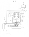
次に、本実施の形態1の荷電粒子線装置による観察工程について説明する。図19は、実施の形態1の荷電粒子線装置による観察工程の一部を示すフロー図である。
<Observation process with charged particle beam equipment>
Next, an observation process using the charged particle beam apparatus according to the first embodiment will be described. FIG. 19 is a flowchart showing a part of an observation process by the charged particle beam apparatus according to the first embodiment.
初めに、真空室4を排気する(ステップS11)。このステップS11では、例えば制御部15により制御された真空ポンプ(排気部)6により、真空配管7を介して、荷電粒子光学鏡筒2および筐体3により区画された真空室4を排気し、真空室4の内部の圧力を真空に減圧する。したがって、真空室4は、真空室4の内部の圧力が真空室4の外部の圧力よりも減圧された状態、すなわち、真空室4の内部と外部との間に圧力差が生じている状態に、維持される。
First, the vacuum chamber 4 is evacuated (step S11). In this step S11, the vacuum chamber 4 defined by the charged particle optical column 2 and the housing 3 is evacuated through the vacuum pipe 7 by the vacuum pump (exhaust unit) 6 controlled by the control unit 15, for example. The pressure inside the vacuum chamber 4 is reduced to a vacuum. Therefore, the vacuum chamber 4 is in a state where the pressure inside the vacuum chamber 4 is reduced more than the pressure outside the vacuum chamber 4, that is, in a state where a pressure difference is generated between the inside and the outside of the vacuum chamber 4. Maintained.
次に、試料12を試料ステージ(保持部)22により保持する(ステップS12)。このステップS12では、試料12を試料ステージ22に載せて保持する。また、試料ステージ(保持部)22または試料ステージ22に保持された試料12が隔膜素子(隔膜部材)18aに接触しないように、例えば制御部15により制御されたZ軸駆動部24により、試料ステージ22のZ軸方向の高さ位置を十分に下げておく。
Next, the sample 12 is held by the sample stage (holding unit) 22 (step S12). In this step S12, the sample 12 is placed on the sample stage 22 and held. Further, the sample stage is controlled by, for example, the Z-axis driving unit 24 controlled by the control unit 15 so that the sample stage (holding unit) 22 or the sample 12 held on the sample stage 22 does not contact the diaphragm element (diaphragm member) 18a. The height position of 22 in the Z-axis direction is sufficiently lowered.
次に、荷電粒子線を発生させる(ステップS13)。このステップS13では、例えばフィラメントを含む電子銃からなる荷電粒子源9により、荷電粒子線を発生させる。
Next, a charged particle beam is generated (step S13). In this step S13, a charged particle beam is generated by the charged particle source 9 made of an electron gun including a filament, for example.
次に、試料12の観察を開始する(ステップS14)。このステップS14では、荷電粒子光学系10の光学レンズ11の条件等を調整し、パーソナルコンピュータ16に試料12の画像を映し、観察を開始する。なお、最初は、次の焦点合わせがスムーズに行えるように、倍率を低倍率にしておく。
Next, observation of the sample 12 is started (step S14). In this step S14, the conditions of the optical lens 11 of the charged particle optical system 10 are adjusted, an image of the sample 12 is displayed on the personal computer 16, and observation is started. Initially, the magnification is set to a low magnification so that the next focusing can be performed smoothly.
次に、Z軸調整による焦点合わせを行う(ステップS15)。このステップS15では、試料12の画像を観察しながらZ軸駆動部24を用いて試料12の高さ位置を徐々に上昇させ、試料12が鮮明に観察されるように、焦点を合わせる。
Next, focusing is performed by adjusting the Z axis (step S15). In this step S15, while observing the image of the sample 12, the height position of the sample 12 is gradually raised using the Z-axis drive unit 24, and the focus is adjusted so that the sample 12 is clearly observed.
次に、X、Y軸調整により所望の観察場所の設定を行う(ステップS16)。このステップS16では、試料12の画像を観察しながらX、Y軸駆動部25を用いて、所望の観察場所に試料12を移動させる。
Next, a desired observation place is set by adjusting the X and Y axes (step S16). In this step S16, while observing the image of the sample 12, the sample 12 is moved to a desired observation location by using the X and Y axis drive unit 25.
次に、倍率調整および焦点微調整を行う(ステップS17)。このステップS17では、倍率の調整、および、Z軸駆動部24の微調整を行う。
Next, magnification adjustment and fine focus adjustment are performed (step S17). In step S17, the magnification is adjusted and the Z-axis drive unit 24 is finely adjusted.
次に、画像取得を開始する(ステップS18)。このステップS18では、画像取得のスイッチを押し、パーソナルコンピュータ16により画像を取得し、取得した画像を保存する。そして、この作業を複数回繰り返すことで、試料12について、所望の観察を行い、画像の取得を行う。
Next, image acquisition is started (step S18). In step S18, the image acquisition switch is pressed, the image is acquired by the personal computer 16, and the acquired image is stored. Then, by repeating this operation a plurality of times, desired observation is performed on the sample 12 and an image is acquired.
次に、試料12を取り出す(ステップS19)。このステップS19では、観察が終了した後、Z軸駆動部24を用いて試料12の高さ位置を下降させ、試料12を隔膜素子18aから遠ざけた後、試料ステージ(保持部)22から試料12を取り出す。また、次の試料を観察する場合は、次の試料に対してステップS12~ステップS19の作業を繰り返す。
Next, the sample 12 is taken out (step S19). In step S19, after the observation is completed, the height position of the sample 12 is lowered using the Z-axis drive unit 24, the sample 12 is moved away from the diaphragm element 18a, and then the sample stage (holding unit) 22 and the sample 12 are moved. Take out. When observing the next sample, the operations in steps S12 to S19 are repeated for the next sample.
なお、図19に示した観察工程のフローは、荷電粒子線装置の操作の一例を示したものであり、各工程の順序は、図19に示した順序に限定されない。したがって、ステップS11~ステップS19の各工程の順序を、適宜変更することができる。
The flow of the observation process shown in FIG. 19 shows an example of the operation of the charged particle beam apparatus, and the order of each process is not limited to the order shown in FIG. Therefore, the order of the steps S11 to S19 can be changed as appropriate.
<隔膜の破損について>
例えば上記特許文献1に記載されたSEMと同様な構造を有するSEMでは、試料は隔膜に載せられる。この場合、隔膜が薄いため、隔膜の面積を大きくすることが難しく、試料を観察できる範囲は隔膜が形成された領域のみとなる。したがって、観察したい部分が隔膜に載るまで、試料を何回も隔膜に載せ直す必要がある。また、隔膜が薄いため、試料を交換する時、または、試料を隔膜に載せ直す時に、隔膜が破損するおそれがある。隔膜が破損した場合に、下方に配置された荷電粒子光学鏡筒に試料または大気が入り込み、荷電粒子源が故障するおそれがある。
<Damage to diaphragm>
For example, in the SEM having the same structure as the SEM described in Patent Document 1, the sample is placed on the diaphragm. In this case, since the diaphragm is thin, it is difficult to increase the area of the diaphragm, and the sample can be observed only in the region where the diaphragm is formed. Therefore, it is necessary to mount the sample on the diaphragm many times until the part to be observed is mounted on the diaphragm. In addition, since the diaphragm is thin, the diaphragm may be damaged when the sample is exchanged or when the sample is placed on the diaphragm. If the diaphragm is damaged, the sample or the atmosphere may enter the charged particle optical column arranged below, and the charged particle source may break down.
一方、上記特許文献2に記載されたSEMと同様な構造を有するSEMでは、試料が隔膜に載せられて保持される構造ではないため、試料を保持することによる隔膜の破損のおそれは少ない。また、隔膜素子に対して試料を移動させることができるため、試料を何回も隔膜に載せ直す必要はない。
On the other hand, in the SEM having the same structure as that of the SEM described in Patent Document 2, since the sample is not held on the diaphragm, there is little risk of damage to the diaphragm due to holding the sample. Further, since the sample can be moved with respect to the diaphragm element, it is not necessary to place the sample on the diaphragm many times.
しかし、高分解能で試料を観察する際に、高倍率で焦点を合わせるため、試料ステージを移動させ、試料ステージに保持されている試料を隔膜素子に近づける必要がある。試料を隔膜素子に近づける際には、例えば使用者が画像を観察しながら試料ステージを移動させることにより、隔膜と試料とが接触しないように注意しながら作業を行う。しかし、隔膜から数十μmの距離まで試料を近づけることもあるため、使用者が注意しながら作業を行ったとしても、隔膜と試料とが接触しやすく、隔膜が破損しやすい。
However, when observing a sample with high resolution, it is necessary to move the sample stage and bring the sample held on the sample stage closer to the diaphragm element in order to focus at high magnification. When the sample is brought close to the diaphragm element, for example, the user moves the sample stage while observing the image, so that the work is performed with care so that the diaphragm and the sample do not come into contact with each other. However, since the sample may be brought closer to the distance of several tens of μm from the diaphragm, even if the user performs the work with care, the diaphragm and the sample are likely to come into contact with each other, and the diaphragm is likely to be damaged.
また、隔膜素子を荷電粒子線装置に取り付ける際、または、交換する際に、隔膜素子が他の部材の上に落下するか、または、他の部材に近づくことで、隔膜と他の部材とが接触しやすく、隔膜が破損しやすい。
In addition, when the diaphragm element is attached to the charged particle beam device or replaced, the diaphragm element falls on another member or approaches the other member, so that the diaphragm and the other member are It is easy to contact and the diaphragm is easily damaged.
特に、試料が配置された空間が大気圧下などの非真空状態に維持され、試料が配置された空間の圧力が真空室の圧力よりも大きい場合には、隔膜素子と試料との間に存在するガスの組成または圧力の変化により、焦点距離が変動する。つまり、真空室の外部の圧力が、真空室の内部の圧力よりも大きく、真空室の内部と外部との間で圧力差がある場合には、焦点距離が変動しやすい。そのため、観察画像を撮像する都度、隔膜素子と試料との距離を調整する必要があり、さらに隔膜と試料とが接触しやすくなり、さらに隔膜が破損しやすくなる。
In particular, when the space where the sample is placed is maintained in a non-vacuum state, such as under atmospheric pressure, and the pressure in the space where the sample is placed is greater than the pressure in the vacuum chamber, it exists between the diaphragm element and the sample. The focal length fluctuates due to the change in the composition or pressure of the gas. That is, when the pressure outside the vacuum chamber is larger than the pressure inside the vacuum chamber and there is a pressure difference between the inside and the outside of the vacuum chamber, the focal length is likely to fluctuate. Therefore, it is necessary to adjust the distance between the diaphragm element and the sample every time an observation image is taken, and the diaphragm and the sample are more likely to come into contact with each other, and the diaphragm is more likely to be damaged.
前述したように、上記特許文献2には、非真空環境で物体を観察するSEMにおいて、STEMモードでは、アパーチャの周りに配置される、高さが動作距離を決定するスペーサを使用して、最大分解能を得るように制御する技術が記載されている。
As described above, in the above-mentioned Patent Document 2, in the SEM for observing an object in a non-vacuum environment, in the STEM mode, a spacer that is arranged around the aperture and whose height determines the operating distance is used. Techniques for controlling to obtain resolution are described.
しかし、特許文献2に記載された技術は、試料を透過する電子線を検出するSTEMモードを用いた測定方法に関するものであり、試料とスペーサとを接触させ、スペーサの高さによって動作距離を決定し、最大分解能を達成するものである。また、特許文献2に記載されたSEMにおいて、アパーチャの周りに配置されるスペーサは、隔膜と試料との距離を一定に保つものであり、隔膜と試料とが接触することを防止するものではない。
However, the technique described in Patent Document 2 relates to a measurement method using a STEM mode that detects an electron beam that passes through a sample. The sample and the spacer are brought into contact with each other, and the operating distance is determined by the height of the spacer. The maximum resolution is achieved. In the SEM described in Patent Document 2, the spacer disposed around the aperture keeps the distance between the diaphragm and the sample constant, and does not prevent the diaphragm and the sample from contacting each other. .
したがって、観察画像を撮像する都度、隔膜と試料との距離を調整する必要がある場合には、特許文献2に記載された、隔膜と試料との距離を一定の高さのスペーサにより決定する方法によっては、隔膜と試料とが接触することを防止することはできない。
Therefore, when it is necessary to adjust the distance between the diaphragm and the sample every time an observation image is captured, the method for determining the distance between the diaphragm and the sample described in Patent Document 2 using a spacer having a certain height In some cases, it is impossible to prevent the diaphragm and the sample from coming into contact with each other.
このように、隔膜と試料とが接触しやすい場合、隔膜が破損しやすくなり、高分解能で安定して観察画像を撮像することができないため、荷電粒子線装置の性能が低下する。
As described above, when the diaphragm and the sample are easily in contact with each other, the diaphragm is likely to be damaged, and an observation image cannot be stably captured with high resolution, so that the performance of the charged particle beam apparatus is deteriorated.
<本実施の形態の主要な特徴と効果>
一方、本実施の形態1の荷電粒子線装置1では、隔膜素子18aには、真空室4の内部の圧力が真空室4の外部の圧力よりも減圧された状態で、真空室4の内部と外部とを気密に隔離するとともに、荷電粒子線を透過させる隔膜19が形成されている。また、隔膜素子18aには、試料ステージ(保持部)22に保持されている試料12と隔膜19とが接触することを防止する緩衝膜(膜部)33が、Z軸方向に沿って、隔膜19よりも試料12側に(試料ステージ22側に)位置するように、形成されている。
<Main features and effects of the present embodiment>
On the other hand, in the charged particle beam apparatus 1 according to the first embodiment, the diaphragm element 18 a has the inside of the vacuum chamber 4 in a state where the pressure inside the vacuum chamber 4 is reduced more than the pressure outside the vacuum chamber 4. A diaphragm 19 is formed that airtightly isolates the outside from the outside and transmits charged particle beams. The diaphragm element 18a has a buffer film (film part) 33 that prevents the sample 12 held on the sample stage (holding part) 22 from contacting the diaphragm 19 along the Z-axis direction. It is formed so as to be located closer to the sample 12 side (to the sample stage 22 side) than 19.
このように、隔膜素子18aに緩衝膜33が形成されていることにより、試料12が隔膜素子18aに近づいたときは、緩衝膜33と試料12が接触する。そのため、隔膜19と試料12とが接触することを防止することができ、隔膜19が破損することを防止することができる。したがって、高分解能で安定して観察画像を撮像することができるため、荷電粒子線装置の性能が向上する。
Thus, when the buffer film 33 is formed on the diaphragm element 18a, the buffer film 33 and the sample 12 come into contact when the sample 12 approaches the diaphragm element 18a. Therefore, it can prevent that the diaphragm 19 and the sample 12 contact, and can prevent that the diaphragm 19 is damaged. Therefore, since an observation image can be captured stably with high resolution, the performance of the charged particle beam apparatus is improved.
また、隔膜素子18aを荷電粒子線装置に取り付ける際、または、交換する際に、隔膜素子18aが他の部材の上に落下したとき、または、他の部材に近づいたときも、緩衝膜33と他の部材とが接触する。そのため、隔膜19と他の部材とが接触することを防止することができ、隔膜19が破損することを防止することができる。
Further, when the diaphragm element 18a is dropped on another member or approaches another member when the diaphragm element 18a is attached to or replaced with the charged particle beam device, the buffer film 33 and Contact with other members. Therefore, it can prevent that the diaphragm 19 and another member contact, and can prevent that the diaphragm 19 is damaged.
特に、試料12が配置された空間が大気圧下などの非真空状態に維持され、試料12が配置された空間の圧力が真空室4の圧力よりも大きい場合には、隔膜素子18aと試料12との間に存在するガスの組成または圧力の変化により、焦点距離が変動する。つまり、真空室4の外部の圧力が、真空室4の内部の圧力よりも大きく、真空室4の内部と外部との間で圧力差がある場合には、焦点距離が変動しやすい。そのため、観察画像を撮像する都度、隔膜素子18aと試料12との距離を調整する必要がある。
In particular, when the space in which the sample 12 is disposed is maintained in a non-vacuum state such as under atmospheric pressure and the pressure in the space in which the sample 12 is disposed is greater than the pressure in the vacuum chamber 4, the diaphragm element 18a and the sample 12 The focal length fluctuates due to a change in the composition or pressure of the gas existing between the two. That is, when the pressure outside the vacuum chamber 4 is larger than the pressure inside the vacuum chamber 4 and there is a pressure difference between the inside and the outside of the vacuum chamber 4, the focal length is likely to fluctuate. Therefore, it is necessary to adjust the distance between the diaphragm element 18a and the sample 12 every time an observation image is taken.
このような場合には、特許文献2に記載された、隔膜と試料との距離を一定の高さのスペーサにより決定する方法によっては、隔膜と試料とが接触することを防止することはできない。しかし、本実施の形態1の隔膜素子18aを用いることで、隔膜19と試料12とが接触することを防止する効果が大きくなる。
In such a case, contact between the diaphragm and the sample cannot be prevented by the method described in Patent Document 2 in which the distance between the diaphragm and the sample is determined by a spacer having a certain height. However, by using the diaphragm element 18a of the first embodiment, the effect of preventing the diaphragm 19 and the sample 12 from contacting each other is increased.
(実施の形態2)
次に、本発明の実施の形態2の荷電粒子線装置について説明する。本実施の形態2の荷電粒子線装置は、隔膜素子(隔膜部材)が、保持基板(基体)を装着するアタッチメントを含み、保持基板が装着されたアタッチメントが筐体の下面部に取り付けられるものである。したがって、本実施の形態2の荷電粒子線装置のうち、アタッチメント以外の各部分については、実施の形態1の荷電粒子線装置における各部分と同一であり、その説明を省略する。また、本実施の形態2の荷電粒子線装置のうちアタッチメント以外の部分による効果についても、実施の形態1の荷電粒子線装置による効果と同一であり、その説明を省略する。
(Embodiment 2)
Next, the charged particle beam apparatus according to the second embodiment of the present invention will be described. In the charged particle beam apparatus according to the second embodiment, the diaphragm element (diaphragm member) includes an attachment for mounting the holding substrate (base), and the attachment to which the holding substrate is mounted is attached to the lower surface portion of the housing. is there. Therefore, in the charged particle beam apparatus of the second embodiment, each part other than the attachment is the same as each part in the charged particle beam apparatus of the first embodiment, and the description thereof is omitted. In addition, the effects of the charged particle beam apparatus according to the second embodiment other than the attachment are the same as the effects of the charged particle beam apparatus according to the first embodiment, and the description thereof is omitted.
なお、以下では、隔膜素子として、図18に示した実施の形態1の第7変形例の隔膜素子(隔膜部材)18hを用いる例について説明する。しかし、隔膜素子18hに代え、実施の形態1の隔膜素子18a、および、実施の形態の第1変形例~第6変形例の隔膜素子18b~18gを用いることもできる。
In the following, an example in which the diaphragm element (diaphragm member) 18h according to the seventh modification of the first embodiment shown in FIG. 18 is used as the diaphragm element will be described. However, the diaphragm element 18a of the first embodiment and the diaphragm elements 18b to 18g of the first to sixth modifications of the embodiment may be used instead of the diaphragm element 18h.
図20は、実施の形態2の荷電粒子線装置のうち、隔膜素子および試料ステージの周辺の構造を示す図である。図21は、実施の形態2のアタッチメントを試料側から見た平面図である。図22は、図21のB-B線に沿った要部断面図である。
FIG. 20 is a diagram showing a structure around the diaphragm element and the sample stage in the charged particle beam apparatus according to the second embodiment. FIG. 21 is a plan view of the attachment of the second embodiment as viewed from the sample side. FIG. 22 is a cross-sectional view of the principal part along the line BB in FIG.
図20~図22に示すように、本実施の形態2の荷電粒子線装置1aにおいて、隔膜素子18hの保持基板30は、アタッチメント(隔膜保持部材、装着体)40に容易に着脱可能に装着される。また、筐体3の下面部(真空室4の壁部)3aには、アタッチメント(装着体)40を支持する支持部41が形成されている。支持部41と、アタッチメント40とは、互いに対応した凹凸形状を含む断面形状を有している。そして、アタッチメント40を、図20において紙面手前側から紙面奥側に向かってスライドさせることで、アタッチメント40を、落下させることなく容易に支持部41に取り付けることができる。つまり、保持基板30が装着されたアタッチメント40が支持部41(筐体3の下面部3a)に取り付けられることで、隔膜素子18hが筐体3の下面部3aに取り付けられる。
As shown in FIGS. 20 to 22, in the charged particle beam apparatus 1a of the second embodiment, the holding substrate 30 of the diaphragm element 18h is detachably attached to the attachment (diaphragm holding member, attachment body) 40. The In addition, a support portion 41 that supports an attachment (mounting body) 40 is formed on the lower surface portion (wall portion of the vacuum chamber 4) 3 a of the housing 3. The support part 41 and the attachment 40 have a cross-sectional shape including a concavo-convex shape corresponding to each other. And the attachment 40 can be easily attached to the support part 41, without dropping, by sliding the attachment 40 toward the back | inner side of a paper surface in FIG. That is, the diaphragm element 18 h is attached to the lower surface portion 3 a of the housing 3 by attaching the attachment 40 to which the holding substrate 30 is mounted to the support portion 41 (the lower surface portion 3 a of the housing 3).
筐体3の下面部3aであって、図20における支持部41の紙面奥側には、アタッチメント40を所定の位置に止めるためのストッパ(図示は省略)が設けられている。ストッパ(図示は省略)は、アタッチメント40が所定の位置に止められたときに、筐体3の下面部3aに形成された開口部3bと、アタッチメント40に保持基板30が装着された隔膜素子18hの隔膜(膜部)19とが、平面視において、重なるように、設けられている。
A stopper (not shown) for stopping the attachment 40 at a predetermined position is provided on the lower surface portion 3a of the housing 3 on the back side of the paper surface of the support portion 41 in FIG. The stopper (not shown) includes an opening 3b formed in the lower surface 3a of the housing 3 when the attachment 40 is stopped at a predetermined position, and a diaphragm element 18h in which the holding substrate 30 is attached to the attachment 40. Are provided so as to overlap with each other in a plan view.
アタッチメント(装着体)40は、好適には、金属を含む材料からなる。アタッチメント40の材料として、金属を含む材料を用いることで、アタッチメント40と筐体3とを電気的に低抵抗で接続することができ、アタッチメント40の電位と筐体3の電位とを等電位とすることができる。さらに、筐体3が接地されており、筐体3の電位が0電位(アース)であるときは、アタッチメント40の電位を0電位(アース)とすることができる。
The attachment (mounting body) 40 is preferably made of a material containing metal. By using a metal-containing material as the material of the attachment 40, the attachment 40 and the housing 3 can be electrically connected with low resistance, and the potential of the attachment 40 and the potential of the housing 3 are made equipotential. can do. Further, when the casing 3 is grounded and the potential of the casing 3 is 0 potential (earth), the potential of the attachment 40 can be 0 potential (ground).
筐体3とアタッチメント40との間には、シール部材42が設けられている。シール部材42は、筐体3とアタッチメント40の間を気密にシールする。シール部材42として、例えばOリングを用いることができる。あるいは、シール部材42を設けることに代え、筐体3とアタッチメント40との間に真空グリースを塗った状態で筐体3とアタッチメント40とを接触させることで、筐体3とアタッチメント40の間を気密にシールすることもできる。
A seal member 42 is provided between the housing 3 and the attachment 40. The seal member 42 hermetically seals between the housing 3 and the attachment 40. As the seal member 42, for example, an O-ring can be used. Alternatively, instead of providing the seal member 42, the housing 3 and the attachment 40 are brought into contact with each other in a state where vacuum grease is applied between the housing 3 and the attachment 40, so that the space between the housing 3 and the attachment 40 is provided. It can also be hermetically sealed.
図21および図22に示すように、アタッチメント(装着体)40は、主面40a、および、主面40aと反対側の主面40bを有する。主面40a側において、アタッチメント40の中央部には、凹部43が設けられており、隔膜素子(隔膜部材)18hの保持基板30は、凹部43に容易に着脱可能に装着される。図21における凹部43の上側、左側には、それぞれ、図21における上下方向、左右方向にスライド移動可能な押さえ冶具44、45が設けられており、押さえ冶具44、45には、押さえ冶具44、45を固定するためのネジ46、47が設けられている。
As shown in FIGS. 21 and 22, the attachment (mounting body) 40 has a main surface 40a and a main surface 40b opposite to the main surface 40a. On the main surface 40a side, a recess 43 is provided in the center of the attachment 40, and the holding substrate 30 of the diaphragm element (diaphragm member) 18h is easily detachably attached to the recess 43. On the upper side and the left side of the concave portion 43 in FIG. 21, holding jigs 44 and 45 that are slidable in the vertical and horizontal directions in FIG. 21 are provided, respectively. Screws 46 and 47 for fixing 45 are provided.
また、凹部43の底面と、凹部43に装着されている保持基板30との間には、シール部材48が設けられている。シール部材48は、アタッチメント40と保持基板30との間を気密にシールする。シール部材48として、好適には、アタッチメント40と保持基板30との間を気密にシールすることができ、アタッチメント40と保持基板30とに損傷を与えないように、柔らかい材料を用いることができ、例えばOリングを用いることができる。あるいは、シール部材48を設けることに代え、アタッチメント40と保持基板30との間に真空グリースを塗った状態で接触させることで、アタッチメント40と保持基板30との間を気密にシールすることもできる。
In addition, a seal member 48 is provided between the bottom surface of the recess 43 and the holding substrate 30 attached to the recess 43. The seal member 48 hermetically seals between the attachment 40 and the holding substrate 30. As the seal member 48, preferably, a soft material can be used so that the attachment 40 and the holding substrate 30 can be hermetically sealed, and the attachment 40 and the holding substrate 30 are not damaged. For example, an O-ring can be used. Alternatively, instead of providing the sealing member 48, the attachment 40 and the holding substrate 30 can be hermetically sealed by contacting the attachment 40 and the holding substrate 30 with vacuum grease applied. .
隔膜素子18hの保持基板30をアタッチメント40に装着するときは、保持基板30を凹部43に装着し、押さえ冶具44、45をスライドさせることで、保持基板30を、凹部43に対して、それぞれ図21における下側、右側に押し当てる。そして、保持基板30を凹部43に対して押し当てた状態で、ネジ46、47により保持基板30を固定する。この押さえ冶具44、45を設けたアタッチメント40を用いることにより、隔膜素子18hを交換した場合でも、隔膜19の位置を、常にアタッチメント40の中心の位置に合わせることができる。そのため、アタッチメント40と支持部41とを組み合わせて用いることで、荷電粒子線が常に隔膜19の中心を通るようになり、試料12を観察するまでの調整時間を短縮することができる。
When the holding substrate 30 of the diaphragm element 18h is attached to the attachment 40, the holding substrate 30 is attached to the recess 43, and the holding jigs 44 and 45 are slid, so that the holding substrate 30 is shown in FIG. 21 is pressed to the lower side and the right side. The holding substrate 30 is fixed with screws 46 and 47 in a state where the holding substrate 30 is pressed against the recess 43. By using the attachment 40 provided with the holding jigs 44 and 45, the position of the diaphragm 19 can always be adjusted to the center position of the attachment 40 even when the diaphragm element 18h is replaced. Therefore, by using the attachment 40 and the support portion 41 in combination, the charged particle beam always passes through the center of the diaphragm 19, and the adjustment time until the sample 12 is observed can be shortened.
図21において、アタッチメント40の中央部よりも左右両側の部分には、ガイド49が設けられている。ガイド49は、保持基板30が装着されたアタッチメント40を、落下させることなく支持部41に取り付けるためのものである。ガイド49は、図20を用いて前述したように、支持部41と、アタッチメント40とが、互いに対応した凹凸形状を含む断面形状を有するように形成されている。
In FIG. 21, guides 49 are provided on the left and right sides of the center of the attachment 40. The guide 49 is for attaching the attachment 40 to which the holding substrate 30 is mounted to the support portion 41 without dropping. As described above with reference to FIG. 20, the guide 49 is formed so that the support portion 41 and the attachment 40 have a cross-sectional shape including a concavo-convex shape corresponding to each other.
図22に示すように、保持基板(基体)30が凹部43に装着されたとき、好適には、保持基板30の主面30aが、アタッチメント40の主面40aと同一面を形成するか、または、主面30aが主面40a上に突出する。これにより、試料ステージ(保持部)22に保持されている試料12とアタッチメント40の主面40aとが接触することを防止することができる。
As shown in FIG. 22, when the holding substrate (base body) 30 is mounted in the recess 43, preferably, the main surface 30a of the holding substrate 30 forms the same surface as the main surface 40a of the attachment 40, or The main surface 30a protrudes on the main surface 40a. Thereby, it can prevent that the sample 12 hold | maintained at the sample stage (holding | holding part) 22 and the main surface 40a of the attachment 40 contact.
隔膜素子として、図18に示した隔膜素子18hまたは図17に示した隔膜素子18gを用いる場合、押さえ冶具44、45は、好適には、導電性の材料からなる。押さえ冶具44、45の材料として、導電性の材料を用いることで、シール膜(膜部)35、押さえ冶具44、45およびアタッチメント40を電気的に低抵抗で接続することができる。これにより、試料12から放出された二次荷電粒子のうち隔膜19を透過または通過しなかったものを、シール膜35、押さえ冶具44、45およびアタッチメント40を介して隔膜素子の外部に逃がすことができる。そのため、緩衝膜33または隔膜19に二次荷電粒子が蓄積されることによる感度低下を防止することができる。
When the diaphragm element 18h shown in FIG. 18 or the diaphragm element 18g shown in FIG. 17 is used as the diaphragm element, the holding jigs 44 and 45 are preferably made of a conductive material. By using a conductive material as the material of the pressing jigs 44 and 45, the sealing film (film part) 35, the pressing jigs 44 and 45, and the attachment 40 can be electrically connected with low resistance. As a result, secondary charged particles emitted from the sample 12 that have not permeated or passed through the diaphragm 19 can be released to the outside of the diaphragm element via the seal film 35, the holding jigs 44 and 45, and the attachment 40. it can. Therefore, it is possible to prevent a decrease in sensitivity due to accumulation of secondary charged particles in the buffer film 33 or the diaphragm 19.
また、図18に示した隔膜素子18hまたは図17に示した隔膜素子18gにおいて、シール膜35が保持基板(基体)30の側面30fにも形成されている場合、シール膜35と押さえ冶具44、45とを電気的にさらに低抵抗で接続することができる。そのため、緩衝膜33または隔膜19に二次荷電粒子が蓄積されることによる感度低下をさらに防止することができる。
Further, in the diaphragm element 18h shown in FIG. 18 or the diaphragm element 18g shown in FIG. 17, when the seal film 35 is also formed on the side surface 30f of the holding substrate (substrate) 30, the seal film 35 and the pressing jig 44, 45 can be electrically connected with lower resistance. Therefore, it is possible to further prevent a decrease in sensitivity due to accumulation of secondary charged particles in the buffer film 33 or the diaphragm 19.
(実施の形態3)
次に、本発明の実施の形態3の荷電粒子線装置について説明する。本実施の形態3の荷電粒子線装置は、実施の形態1の荷電粒子線装置に、ガスを供給する供給部を追加したものである。したがって、本実施の形態3の荷電粒子線装置のうち、供給部以外の各部分については、実施の形態1の荷電粒子線装置における各部分と同一であり、その説明を省略する。また、本実施の形態3の荷電粒子線装置のうち供給部以外の部分による効果についても、実施の形態1の荷電粒子線装置による効果と同一であり、その説明を省略する。
(Embodiment 3)
Next, the charged particle beam apparatus according to the third embodiment of the present invention will be described. The charged particle beam apparatus according to the third embodiment is obtained by adding a supply unit that supplies gas to the charged particle beam apparatus according to the first embodiment. Therefore, in the charged particle beam apparatus according to the third embodiment, each part other than the supply unit is the same as each part in the charged particle beam apparatus according to the first embodiment, and a description thereof is omitted. In addition, the effects of the charged particle beam apparatus of the third embodiment other than the supply unit are the same as the effects of the charged particle beam apparatus of the first embodiment, and the description thereof is omitted.
図23は、実施の形態3の荷電粒子線装置の全体構成図である。
FIG. 23 is an overall configuration diagram of the charged particle beam apparatus according to the third embodiment.
図23に示すように、本実施の形態3の荷電粒子線装置1bでは、隔膜素子(隔膜部材)18aと試料12との間にガスを供給する供給部50が設けられている。供給部50は、ガスボンベ51、ガス供給管52およびガス制御用バルブ53を有する。ガスボンベ51は、真空室4の外部に設けられている。ガス供給管52の一端は、ガスボンベ51に接続されており、ガス供給管52の他端は、隔膜素子18aの付近で開口している。ガス供給管52の途中には、ガス制御用バルブ53が設けられており、ガス制御用バルブ53の開閉動作および開度は、制御部15により制御される。
As shown in FIG. 23, in the charged particle beam apparatus 1b of the third embodiment, a supply unit 50 for supplying gas is provided between the diaphragm element (diaphragm member) 18a and the sample 12. The supply unit 50 includes a gas cylinder 51, a gas supply pipe 52, and a gas control valve 53. The gas cylinder 51 is provided outside the vacuum chamber 4. One end of the gas supply pipe 52 is connected to the gas cylinder 51, and the other end of the gas supply pipe 52 opens near the diaphragm element 18a. A gas control valve 53 is provided in the middle of the gas supply pipe 52, and the opening / closing operation and the opening degree of the gas control valve 53 are controlled by the control unit 15.
このような構成において、制御部15によりガス制御用バルブ53の開閉動作および開度を制御することで、隔膜素子18aと試料12との間に、ガス供給管52を介してガスを供給することができる。
In such a configuration, gas is supplied between the diaphragm element 18a and the sample 12 via the gas supply pipe 52 by controlling the opening / closing operation and the opening degree of the gas control valve 53 by the control unit 15. Can do.
なお、ガスボンベ51については、荷電粒子線装置1bの一部として用意されたものを用いてもよいが、荷電粒子線装置1bとは別に用意されたものを用いてもよい。
Note that the gas cylinder 51 may be prepared as a part of the charged particle beam apparatus 1b, but may be prepared separately from the charged particle beam apparatus 1b.
隔膜素子18aと試料12との間に空気が存在する場合、隔膜(膜部)19を透過または通過した一次荷電粒子線および試料12から放出された二次荷電粒子が、空気に含まれる気体分子により散乱される。そのため、試料12に到達する一次荷電粒子線の量が減少し、検出器13に到達する二次荷電粒子の量が減少する。一方、隔膜(膜部)19と試料12との間に、例えば空気の平均分子量よりも小さい分子量を有する気体分子からなるガス、すなわち空気よりも軽いガスを供給することで、一次荷電粒子線および二次荷電粒子が散乱される確率を小さくすることができる。これにより、試料12に到達する一次荷電粒子線の量を増加させることができ、検出器13に到達する二次荷電粒子の量を増加させることができる。
When air exists between the diaphragm element 18a and the sample 12, the primary charged particle beam that has passed through or passed through the diaphragm (film part) 19 and the secondary charged particles emitted from the sample 12 are gas molecules contained in the air. It is scattered by. Therefore, the amount of the primary charged particle beam that reaches the sample 12 decreases, and the amount of the secondary charged particle that reaches the detector 13 decreases. On the other hand, by supplying a gas composed of gas molecules having a molecular weight smaller than the average molecular weight of air, for example, a gas lighter than air, between the diaphragm (membrane part) 19 and the sample 12, primary charged particle beams and The probability that the secondary charged particles are scattered can be reduced. Thereby, the amount of primary charged particle beams reaching the sample 12 can be increased, and the amount of secondary charged particles reaching the detector 13 can be increased.
したがって、供給部50により供給するガスとして、例えば窒素(N2)ガスまたは水蒸気ガスなどの、空気よりも軽いガスを用いることができ、これにより、画像のS/N比を改善することができる。また、供給部50により供給するガスとして、好適には、例えばヘリウム(He)ガスまたは水素(H2)ガスなどの、N2ガスまたは水蒸気ガスの分子量よりも小さい分子量を有するガスを用いることができる。このようなガスを用いることで、画像のS/N比をさらに改善することができる。
Therefore, a gas that is lighter than air, such as nitrogen (N 2 ) gas or water vapor gas, can be used as the gas supplied by the supply unit 50, thereby improving the S / N ratio of the image. . Further, as the gas supplied by the supply unit 50, a gas having a molecular weight smaller than that of N 2 gas or water vapor gas, such as helium (He) gas or hydrogen (H 2 ) gas, is preferably used. it can. By using such a gas, the S / N ratio of the image can be further improved.
なお、本実施の形態3の荷電粒子線装置1bによる観察工程は、図19のステップS15~ステップS18の工程を、隔膜素子18aと試料12との間にガスを供給しながら行う点を除き、実施の形態1の荷電粒子線装置1による観察工程と同様に行うことができる。
The observation process by the charged particle beam device 1b according to the third embodiment is performed except that the processes in steps S15 to S18 in FIG. 19 are performed while gas is supplied between the diaphragm element 18a and the sample 12. It can carry out similarly to the observation process by the charged particle beam apparatus 1 of Embodiment 1. FIG.
(実施の形態4)
次に、本発明の実施の形態4の荷電粒子線装置について説明する。実施の形態1の荷電粒子線装置は、荷電粒子光学鏡筒および筐体を備えており、真空室が荷電粒子光学鏡筒および筐体により区画されていた。それに対して、本実施の形態4の荷電粒子線装置は、荷電粒子光学鏡筒および第1筐体に加え、第2筐体を備えており、第1筐体に第2筐体を装着することで、荷電粒子光学鏡筒、第1筐体および第2筐体により真空室が区画される。
(Embodiment 4)
Next, a charged particle beam apparatus according to the fourth embodiment of the present invention will be described. The charged particle beam apparatus according to the first embodiment includes a charged particle optical barrel and a casing, and the vacuum chamber is partitioned by the charged particle optical barrel and the casing. In contrast, the charged particle beam device according to the fourth embodiment includes a second housing in addition to the charged particle optical column and the first housing, and the second housing is mounted on the first housing. Thus, the vacuum chamber is defined by the charged particle optical column, the first casing, and the second casing.
なお、以下では、本実施の形態4の荷電粒子線装置を卓上型の走査型電子顕微鏡に適用した例について説明する。しかし、本実施の形態4の荷電粒子線装置が、イオン顕微鏡など、他の各種の荷電粒子線装置に適用できることはいうまでもない。
In the following, an example in which the charged particle beam apparatus according to the fourth embodiment is applied to a desktop scanning electron microscope will be described. However, it goes without saying that the charged particle beam apparatus according to the fourth embodiment can be applied to other various charged particle beam apparatuses such as an ion microscope.
<走査型電子顕微鏡の構成>
図24は、実施の形態4の走査型電子顕微鏡の全体構成図である。
<Configuration of scanning electron microscope>
FIG. 24 is an overall configuration diagram of a scanning electron microscope according to the fourth embodiment.
図24に示すように、本実施の形態4の走査型電子顕微鏡(荷電粒子線装置)1cには、荷電粒子光学鏡筒2、筐体3cおよび筐体部材(荷電粒子線装置用部材)56が設けられている。筐体部材56は、筐体55、隔膜素子(隔膜部材)18a、試料ステージ(保持部)22、Z軸駆動部24および蓋部材57を含む。筐体3cに筐体部材56の筐体55を装着することで、荷電粒子光学鏡筒2、筐体3cおよび筐体55により真空室4aが区画される。
As shown in FIG. 24, a scanning electron microscope (charged particle beam device) 1c according to the fourth embodiment includes a charged particle optical column 2, a housing 3c, and a housing member (charged particle beam device member) 56. Is provided. The casing member 56 includes a casing 55, a diaphragm element (diaphragm member) 18 a, a sample stage (holding section) 22, a Z-axis driving section 24, and a lid member 57. By attaching the housing 55 of the housing member 56 to the housing 3c, the vacuum chamber 4a is partitioned by the charged particle optical barrel 2, the housing 3c, and the housing 55.
実施の形態1における荷電粒子光学鏡筒2と同様に、本実施の形態4における荷電粒子光学鏡筒2も、例えば筐体3cの上側に、荷電粒子光学鏡筒2の下部が筐体3cの内部に突出するように、設けられている。荷電粒子光学鏡筒2は、シール部材(Oリング)5を介して筐体3cに取り付けられており、筐体55は、シール部材(Oリング)5aを介して筐体3cに取り付けられている。したがって、荷電粒子光学鏡筒2、筐体3cおよび筐体55により区画された真空室4aは、気密に設けられている。
Similar to the charged particle optical column 2 in the first embodiment, the charged particle optical column 2 in the fourth embodiment also has, for example, an upper side of the housing 3c and a lower portion of the charged particle optical column 2 of the housing 3c. It is provided so as to protrude inside. The charged particle optical column 2 is attached to the housing 3c via a seal member (O-ring) 5, and the housing 55 is attached to the housing 3c via a seal member (O-ring) 5a. . Therefore, the vacuum chamber 4a defined by the charged particle optical barrel 2, the housing 3c, and the housing 55 is provided in an airtight manner.
図24に示す例では、筐体3cの例えば側面部3dに開口部3eが設けられている。筐体55は、例えば開口部3eを塞ぐように設けられた側面部55aと、側面部55aと一体に設けられており、筐体3cの開口部3eから、筐体3cの中央部に向かって引っ込むように設けられた凹部55bとを有する。凹部55bは、筐体55が筐体3cに取り付けられときに、凹部55bにより区画された試料室58が、荷電粒子光学鏡筒2の下方に位置するように、設けられている。
In the example shown in FIG. 24, an opening 3e is provided in, for example, the side surface 3d of the housing 3c. The housing 55 is provided integrally with the side surface portion 55a provided so as to close the opening 3e and the side surface portion 55a, for example, from the opening 3e of the housing 3c toward the center of the housing 3c. And a recess 55b provided to retract. The recess 55b is provided such that the sample chamber 58 defined by the recess 55b is positioned below the charged particle optical column 2 when the housing 55 is attached to the housing 3c.
筐体55には、蓋部材57が設けられている。蓋部材57は、筐体55に着脱可能に取り付けられるものであり、筐体55に蓋部材57を取り付けることで、筐体55および蓋部材57により、試料室58が区画される。また、試料室58の内部の空間は、真空室4aの外部の空間である。蓋部材57は、筐体55にシール部材(Oリング)59を介して取り付けられている。したがって、筐体55および蓋部材57により区画された試料室58は、気密に設けられている。
The casing 55 is provided with a lid member 57. The lid member 57 is detachably attached to the housing 55, and the sample chamber 58 is partitioned by the housing 55 and the lid member 57 by attaching the lid member 57 to the housing 55. The space inside the sample chamber 58 is a space outside the vacuum chamber 4a. The lid member 57 is attached to the housing 55 via a seal member (O-ring) 59. Therefore, the sample chamber 58 partitioned by the housing 55 and the lid member 57 is provided in an airtight manner.
図24に示す例では、蓋部材57は、筐体55の側面部55aにシール部材59を介して取り付けられており、試料室58は、蓋部材57および凹部55bにより区画される。また、蓋部材57は、後述する図26を用いて説明するように、図24に示す位置から左側にスライドする(移動する)ことで、筐体55から取り外された状態となる。
In the example shown in FIG. 24, the lid member 57 is attached to the side surface portion 55a of the housing 55 via a seal member 59, and the sample chamber 58 is partitioned by the lid member 57 and the recess 55b. Further, as will be described later with reference to FIG. 26, the lid member 57 is removed from the housing 55 by sliding (moving) to the left from the position shown in FIG. 24.
荷電粒子光学鏡筒2、筐体3cおよび筐体55により区画された真空室4aの外部には、真空ポンプ(排気部)6が設けられている。真空ポンプ6は、荷電粒子光学鏡筒2および筐体3cに、真空配管7により接続されている。すなわち、真空ポンプ6は、真空室4aに接続されている。
A vacuum pump (exhaust unit) 6 is provided outside the vacuum chamber 4a defined by the charged particle optical column 2, the casing 3c, and the casing 55. The vacuum pump 6 is connected to the charged particle optical barrel 2 and the housing 3c by a vacuum pipe 7. That is, the vacuum pump 6 is connected to the vacuum chamber 4a.
走査型電子顕微鏡(荷電粒子線装置)1cの使用時には、真空室4aは、真空ポンプ6により排気され、真空室4aの内部の圧力が真空に減圧される。すなわち、真空室4aは、真空ポンプ6により排気され、真空室4aの内部の圧力が、真空室4aの外部の圧力よりも減圧された状態に、維持される。
When using the scanning electron microscope (charged particle beam apparatus) 1c, the vacuum chamber 4a is evacuated by the vacuum pump 6, and the pressure inside the vacuum chamber 4a is reduced to a vacuum. That is, the vacuum chamber 4a is evacuated by the vacuum pump 6, and the pressure inside the vacuum chamber 4a is maintained in a state where the pressure is reduced more than the pressure outside the vacuum chamber 4a.
なお、本実施の形態4でも、実施の形態1と同様に、真空ポンプ6は1つのみ示されているが、2つ以上あってもよい。
In the fourth embodiment, only one vacuum pump 6 is shown as in the first embodiment, but there may be two or more.
本実施の形態4でも、実施の形態1と同様に、筐体3cには、リークバルブ8が設けられている。リークバルブ8は、荷電粒子光学鏡筒2、筐体3cおよび筐体55により区画された真空室4aを大気開放するためのものである。
Also in the fourth embodiment, a leak valve 8 is provided in the housing 3c, as in the first embodiment. The leak valve 8 is for opening the vacuum chamber 4a defined by the charged particle optical barrel 2, the casing 3c, and the casing 55 to the atmosphere.
荷電粒子光学鏡筒2、制御系14の構成は、それぞれ実施の形態1の荷電粒子線装置1における荷電粒子光学鏡筒2、制御系14と同様にすることができる。また、実施の形態1と同様に、荷電粒子光学鏡筒2のうち筐体3cの内部に突出した部分には、検出器13が設けられている。
The configurations of the charged particle optical column 2 and the control system 14 can be the same as those of the charged particle optical column 2 and the control system 14 in the charged particle beam apparatus 1 of the first embodiment, respectively. Similarly to the first embodiment, a detector 13 is provided in a portion of the charged particle optical column 2 that protrudes into the housing 3c.
<試料室の内部>
筐体55であって、真空室4aと試料室58とを区画する部分には、実施の形態1と同様に、隔膜素子(隔膜部材)18aが設けられている。図24に示す例では、筐体55の凹部(真空室4aの壁部)55bであって、荷電粒子光学鏡筒2の下方に位置する部分に、隔膜素子18aが設けられている。隔膜素子18aは、一次荷電粒子線を透過または通過させる隔膜19を含み、真空室4aの内部と試料室58の内部とを気密に隔離する。
<Inside of sample chamber>
As in the first embodiment, a diaphragm element (diaphragm member) 18 a is provided in a portion of the housing 55 that divides the vacuum chamber 4 a and the sample chamber 58. In the example shown in FIG. 24, a diaphragm element 18 a is provided in a concave portion (wall portion of the vacuum chamber 4 a) 55 b of the housing 55, which is positioned below the charged particle optical column 2. The diaphragm element 18a includes a diaphragm 19 that transmits or passes the primary charged particle beam, and hermetically isolates the inside of the vacuum chamber 4a from the inside of the sample chamber 58.
本実施の形態4では、隔膜素子として、実施の形態1と同様に、隔膜素子18aを用いる場合を、代表例として説明する。しかし、隔膜素子として、隔膜素子18aに代え、実施の形態1の第1変形例~第7変形例で説明した隔膜素子18b~18hを用いることができる。
In the fourth embodiment, the case where the diaphragm element 18a is used as the diaphragm element as in the first embodiment will be described as a representative example. However, as the diaphragm element, the diaphragm elements 18b to 18h described in the first to seventh modifications of the first embodiment can be used instead of the diaphragm element 18a.
図24に示す例では、隔膜素子18aの保持基板は、実施の形態2と同様に、アタッチメント(隔膜保持部材、装着体)40に容易に着脱可能に装着される。また、筐体55の凹部55bには、実施の形態2と同様に、アタッチメント40を支持する支持部41が形成されている。
In the example shown in FIG. 24, the holding substrate of the diaphragm element 18a is easily detachably attached to the attachment (diaphragm holding member, attachment body) 40 as in the second embodiment. Further, as in the second embodiment, a support portion 41 that supports the attachment 40 is formed in the recess 55 b of the housing 55.
なお、隔膜素子18aを筐体55に取り付ける方法は、アタッチメント40を用いる方法に限られない。例えば、実施の形態1で説明したように、隔膜素子18aは、隔膜19の周囲の部分が、接着部材21(図2参照)により筐体55の凹部55bに形成された開口部の周囲の部分に接着されることで、筐体55に取り付けられていてもよい。
The method of attaching the diaphragm element 18a to the housing 55 is not limited to the method using the attachment 40. For example, as described in the first embodiment, the diaphragm element 18a has a portion around the opening formed in the recess 55b of the housing 55 by the adhesive member 21 (see FIG. 2). It may be attached to the housing 55 by being adhered to.
真空室4aの外部であって試料室58の内部には、試料ステージ(保持部)22が設けられている。実施の形態1と同様に、試料ステージ22は、試料12を保持するためのものである。本実施の形態4では、試料ステージ22は、支持体60上に組み立てられており、支持体60は、蓋部材57に取り付けられている。したがって、試料ステージ22は、蓋部材57に取り付けられている。
A sample stage (holding unit) 22 is provided outside the vacuum chamber 4 a and inside the sample chamber 58. Similar to the first embodiment, the sample stage 22 is for holding the sample 12. In the fourth embodiment, the sample stage 22 is assembled on the support body 60, and the support body 60 is attached to the lid member 57. Therefore, the sample stage 22 is attached to the lid member 57.
また、試料室58の内部には、Z軸駆動部24およびX、Y軸駆動部25が設けられている。Z軸駆動部24は、実施の形態1と同様に、試料ステージ22を例えば鉛直方向であるZ軸方向に移動駆動し、試料ステージ22の高さ位置を変えることで、試料ステージ22に保持されている試料12と隔膜素子18aとのZ軸方向に沿った距離を調整する。X、Y軸駆動部25は、実施の形態1と同様に、試料ステージ22を例えば水平面内で互いに交差する2方向であるX軸方向およびY軸方向に移動駆動することで、試料ステージ22に保持されている試料12を、X軸方向およびY軸方向に移動させる。
Further, inside the sample chamber 58, a Z-axis drive unit 24 and an X and Y-axis drive unit 25 are provided. The Z-axis drive unit 24 is held by the sample stage 22 by moving and driving the sample stage 22 in, for example, the vertical Z-axis direction and changing the height position of the sample stage 22 as in the first embodiment. The distance along the Z-axis direction between the sample 12 and the diaphragm element 18a is adjusted. As in the first embodiment, the X and Y axis driving unit 25 moves and drives the sample stage 22 in, for example, the X axis direction and the Y axis direction which are two directions intersecting each other in the horizontal plane. The held sample 12 is moved in the X-axis direction and the Y-axis direction.
蓋部材57は、前述したように、筐体55に着脱可能に取り付けられるものである。具体的には、蓋部材57は、例えば底板61、および、底板61に固定支持されている筐体55に対して、スライド可能に(引き出し可能に)設けられている。このような構成により、後述する図26を用いて説明するように、蓋部材57を図24中左側方向にスライドさせることで試料ステージ22を試料室58の外部に引き出すことができ、試料ステージ22により保持する試料12を交換することができる。
The lid member 57 is detachably attached to the housing 55 as described above. Specifically, the lid member 57 is provided so as to be slidable (can be pulled out) with respect to, for example, the bottom plate 61 and the housing 55 fixedly supported by the bottom plate 61. With such a configuration, the sample stage 22 can be pulled out of the sample chamber 58 by sliding the lid member 57 in the left direction in FIG. Thus, the sample 12 held can be exchanged.
また、蓋部材57は、前述したように、筐体55とシール部材(Oリング)59を介して取り付けられることで、筐体55に対して固定されるため、試料12を観察している間、支持板60が動かないように設計されている。
In addition, as described above, the lid member 57 is fixed to the casing 55 by being attached via the casing 55 and the seal member (O-ring) 59, so that the sample 12 is being observed. The support plate 60 is designed not to move.
図24に示すように、本実施の形態4の走査型電子顕微鏡(荷電粒子線装置)1cでは、隔膜素子(隔膜部材)18aと試料12との間にガスを供給する供給部50aが設けられている。供給部50aは、ガスボンベ51、ガス供給管52、ガス制御用バルブ53、圧力計63および圧力調整弁64を有する。ガスボンベ51は、真空室4aの外部に設けられている。ガス供給管52の一端は、ガスボンベ51に接続されており、ガス供給管52の他端は、試料室58の内部であって隔膜素子18aの付近で開口している。ガス供給管52の途中には、ガス制御用バルブ53が設けられている。ガス制御用バルブ53および圧力調整弁64の開閉動作および開度は、圧力計63の測定値に基づいて、制御部15により制御される。
As shown in FIG. 24, in the scanning electron microscope (charged particle beam apparatus) 1c according to the fourth embodiment, a supply unit 50a for supplying gas is provided between the diaphragm element (diaphragm member) 18a and the sample 12. ing. The supply unit 50 a includes a gas cylinder 51, a gas supply pipe 52, a gas control valve 53, a pressure gauge 63, and a pressure adjustment valve 64. The gas cylinder 51 is provided outside the vacuum chamber 4a. One end of the gas supply pipe 52 is connected to the gas cylinder 51, and the other end of the gas supply pipe 52 is opened inside the sample chamber 58 and in the vicinity of the diaphragm element 18a. A gas control valve 53 is provided in the middle of the gas supply pipe 52. The opening / closing operation and the opening degree of the gas control valve 53 and the pressure regulating valve 64 are controlled by the control unit 15 based on the measured value of the pressure gauge 63.
このような構成において、制御部15によりガス制御用バルブ53の開閉動作および開度を制御することで、隔膜素子18aと試料12との間に、ガス供給管52を介してガスを供給することができる。また、制御部15により圧力調整弁64の開閉動作および開度を制御することで、試料室58の内部を、ガス供給管52を介して供給されたガスで容易に置換することができる。
In such a configuration, gas is supplied between the diaphragm element 18a and the sample 12 via the gas supply pipe 52 by controlling the opening / closing operation and the opening degree of the gas control valve 53 by the control unit 15. Can do. Further, by controlling the opening / closing operation and the opening degree of the pressure adjustment valve 64 by the control unit 15, the inside of the sample chamber 58 can be easily replaced with the gas supplied through the gas supply pipe 52.
なお、ガスボンベ51については、走査型電子顕微鏡1cの一部として用意されたものを用いてもよいが、走査型電子顕微鏡1cとは別に用意されたものを用いてもよい。
The gas cylinder 51 may be prepared as a part of the scanning electron microscope 1c, or may be prepared separately from the scanning electron microscope 1c.
実施の形態3で前述したように、隔膜(膜部)19と試料12との間に、空気よりも軽いガスを供給することで、隔膜19を透過または通過した一次荷電粒子線および試料12から放出された二次荷電粒子が散乱される確率を小さくすることができる。これにより、試料12に到達する一次荷電粒子線の量を増加させることができ、検出器13に到達する二次荷電粒子の量を増加させることができる。
As described above in the third embodiment, by supplying a gas lighter than air between the diaphragm (membrane part) 19 and the sample 12, the primary charged particle beam that has permeated or passed through the diaphragm 19 and the sample 12 are used. The probability that the emitted secondary charged particles are scattered can be reduced. Thereby, the amount of primary charged particle beams reaching the sample 12 can be increased, and the amount of secondary charged particles reaching the detector 13 can be increased.
したがって、供給部50aにより供給するガスとして、例えば窒素(N2)ガスまたは水蒸気ガスなどの、空気よりも軽いガスを用いることができ、これにより、画像のS/N比を改善することができる。また、供給部50aにより供給するガスとして、好適には、例えばHeガスまたはH2ガスなどの、N2ガスまたは水蒸気ガスの分子量よりも小さい分子量を有するガスを用いることができ、これにより、画像のS/N比をさらに改善することができる。
Therefore, a gas that is lighter than air, such as nitrogen (N 2 ) gas or water vapor gas, can be used as the gas supplied by the supply unit 50a, thereby improving the S / N ratio of the image. . Further, as the gas supplied by the supply unit 50a, a gas having a molecular weight smaller than the molecular weight of N 2 gas or water vapor gas, such as He gas or H 2 gas, can be preferably used. The S / N ratio can be further improved.
このように、供給部50aにより供給するガスとして、空気よりも軽いガスを用いる場合には、供給されたガスは、試料室58の内部のうち上部に溜まりやすい。したがって、好適には、圧力調整弁64は、蓋部材57の下部に設けられる。また、供給部50aによるガスの供給を開始する際に、ガス供給管52からのガスを供給するとともに、圧力調整弁64を開けて試料室58の内部から空気を排出する。これにより、試料室58の内部を、供給部50aにより供給されたガスで容易に置換することができる。
Thus, when a gas lighter than air is used as the gas supplied by the supply unit 50 a, the supplied gas tends to accumulate in the upper part of the inside of the sample chamber 58. Therefore, the pressure regulating valve 64 is preferably provided at the lower part of the lid member 57. Further, when the supply of gas by the supply unit 50 a is started, the gas is supplied from the gas supply pipe 52 and the pressure adjustment valve 64 is opened to discharge air from the sample chamber 58. Thereby, the inside of the sample chamber 58 can be easily replaced with the gas supplied from the supply unit 50a.
あるいは、圧力調整弁64に代えて、三方弁を設け、三方弁の一方を真空ポンプ(排気部)6と接続してもよい。このとき、試料室58には、三方弁を介して真空ポンプ6が接続される。また、供給部50aによるガスの供給を開始する前に、ガス制御用バルブ53を閉じた状態で、三方弁を切り替えて真空ポンプ6により試料室58を排気し、その後、ガス制御用バルブ53を開く。これにより、試料室58の内部を、供給部50aにより供給されたガスでさらに容易に置換することができる。
Alternatively, instead of the pressure regulating valve 64, a three-way valve may be provided, and one of the three-way valves may be connected to the vacuum pump (exhaust unit) 6. At this time, the vacuum pump 6 is connected to the sample chamber 58 via a three-way valve. Before starting the gas supply by the supply unit 50a, the three-way valve is switched while the gas control valve 53 is closed, the sample chamber 58 is exhausted by the vacuum pump 6, and then the gas control valve 53 is turned on. open. Thereby, the inside of the sample chamber 58 can be more easily replaced with the gas supplied by the supply unit 50a.
なお、試料室58に真空ポンプ6を接続する場合には、試料室58の内部の圧力が、真空室4aの内部の圧力よりは高いが、大気圧よりも減圧された状態で、試料12の観察をすることができる。すなわち、試料室58の内部の圧力が、真空室4aの内部の圧力との間に圧力差があるものの、大気圧よりも減圧された状態で、試料12の観察をすることができる。
Note that when the vacuum pump 6 is connected to the sample chamber 58, the pressure inside the sample chamber 58 is higher than the pressure inside the vacuum chamber 4a, but in a state where the pressure of the sample 12 is reduced to less than atmospheric pressure. Can observe. That is, the sample 12 can be observed in a state where the pressure inside the sample chamber 58 is lower than the atmospheric pressure although there is a pressure difference between the pressure inside the sample chamber 58 and the pressure inside the vacuum chamber 4a.
本実施の形態4では、筐体部材56全体が走査型電子顕微鏡(荷電粒子線装置)1cに取り付け可能に設けられており、筐体55が筐体3cに取り付け可能に設けられている。また、筐体55を筐体3cに取り付けることで、荷電粒子光学鏡筒2、筐体3cおよび筐体55により区画される真空室4aが気密に設けられる。真空ポンプ6により真空室4aの内部の圧力が試料室58の内部の圧力よりも減圧された状態で、真空室4aの内部を通り、筐体55に設けられた隔膜素子18aを透過した一次荷電粒子線を、試料室58の内部で保持されている試料12に走査して照射する。
In the fourth embodiment, the entire casing member 56 is provided so as to be attachable to the scanning electron microscope (charged particle beam apparatus) 1c, and the casing 55 is provided so as to be attachable to the casing 3c. Further, by attaching the housing 55 to the housing 3c, the vacuum chamber 4a defined by the charged particle optical barrel 2, the housing 3c, and the housing 55 is provided in an airtight manner. The primary charge passing through the inside of the vacuum chamber 4a and passing through the diaphragm element 18a provided in the housing 55 in a state where the pressure inside the vacuum chamber 4a is reduced by the vacuum pump 6 from the pressure inside the sample chamber 58. The particle beam scans and irradiates the sample 12 held inside the sample chamber 58.
また、本実施の形態4では、真空状態で試料を観察するための真空SEMに、筐体部材56をオプションとして装着することで、既設の真空SEMを、大気圧下などの非真空状態で試料を観察するための非真空SEMに、容易に改良することができる。したがって、非真空SEMを導入する際に必要なコストを低減することができる。
In the fourth embodiment, the housing member 56 is optionally attached to a vacuum SEM for observing the sample in a vacuum state, so that the existing vacuum SEM can be used in a non-vacuum state such as under atmospheric pressure. Can be easily improved to a non-vacuum SEM for observing. Therefore, the cost required when introducing the non-vacuum SEM can be reduced.
<走査型電子顕微鏡による観察工程>
次に、本実施の形態4の走査型電子顕微鏡1cによる観察工程について説明する。図25は、実施の形態4の走査型電子顕微鏡による観察工程の一部を示すフロー図である。図26は、実施の形態4の観察工程における走査型電子顕微鏡の全体構成図である。
<Observation process by scanning electron microscope>
Next, an observation process using the scanning electron microscope 1c according to the fourth embodiment will be described. FIG. 25 is a flowchart showing a part of the observation process by the scanning electron microscope of the fourth embodiment. FIG. 26 is an overall configuration diagram of a scanning electron microscope in the observation process of the fourth embodiment.
初めに、真空室4aを排気する(ステップS21)。このステップS21では、例えば制御部15により制御された真空ポンプ(排気部)6により、真空配管7を介して、荷電粒子光学鏡筒2、筐体3cおよび筐体55により区画された真空室4aを排気し、真空室4aの内部の圧力を真空に減圧する。したがって、真空室4aは、真空室4aの内部の圧力が真空室4aの外部であって試料室58の内部の圧力よりも減圧された状態、すなわち、真空室4aの内部と真空室4aの外部(試料室58の内部)との間に圧力差が生じている状態に、維持される。
First, the vacuum chamber 4a is evacuated (step S21). In this step S21, for example, the vacuum chamber 4a partitioned by the charged particle optical column 2, the housing 3c, and the housing 55 through the vacuum pipe 7 by the vacuum pump (exhaust unit) 6 controlled by the control unit 15. And the pressure inside the vacuum chamber 4a is reduced to a vacuum. Accordingly, the vacuum chamber 4a is in a state in which the pressure inside the vacuum chamber 4a is outside the vacuum chamber 4a and lower than the pressure inside the sample chamber 58, that is, inside the vacuum chamber 4a and outside the vacuum chamber 4a. It is maintained in a state where there is a pressure difference with (inside the sample chamber 58).
次に、試料12を試料ステージ(保持部)22により保持する(ステップS22)。このステップS22では、試料12を試料ステージ22に載せて保持する。図26に示すように、蓋部材57をスライドさせ、支持板60上にある試料ステージ22を試料室58から引き出した状態で、試料12を試料ステージ22に載せて保持する。また、実施の形態1におけるステップS12の工程と同様に、試料ステージ22に保持された試料12が隔膜素子(隔膜部材)18aに接触しないように、試料ステージ22のZ軸方向の高さ位置を十分に下げておく。
Next, the sample 12 is held by the sample stage (holding unit) 22 (step S22). In this step S22, the sample 12 is placed on the sample stage 22 and held. As shown in FIG. 26, the lid member 57 is slid and the sample 12 is placed on the sample stage 22 and held while the sample stage 22 on the support plate 60 is pulled out from the sample chamber 58. Similarly to the step S12 in the first embodiment, the height position of the sample stage 22 in the Z-axis direction is set so that the sample 12 held on the sample stage 22 does not contact the diaphragm element (diaphragm member) 18a. Lower it enough.
なお、試料室58の内部の圧力と大気圧との間に圧力差があった場合には、蓋部材57をスライドさせる(引き出す)際には、圧力調整弁64を開けることで、試料室58の内部の圧力を大気圧にすることができる。
When there is a pressure difference between the pressure inside the sample chamber 58 and the atmospheric pressure, the sample chamber 58 is opened by opening the pressure adjustment valve 64 when the lid member 57 is slid (drawn). The pressure inside can be set to atmospheric pressure.
次に、荷電粒子線を発生させる(ステップS23)。このステップS23では、例えばフィラメントを含む電子銃からなる荷電粒子源9により、荷電粒子線を発生させる。
Next, a charged particle beam is generated (step S23). In step S23, a charged particle beam is generated by the charged particle source 9 made of an electron gun including a filament, for example.
次に、試料12の観察を開始する(ステップS24)。このステップS24では、荷電粒子光学系10の光学レンズ11の条件等を調整し、パーソナルコンピュータ16に試料12の画像を映し、観察を開始する。なお、最初は、次の焦点合わせがスムーズに行えるように、倍率を低倍率にしておく。
Next, observation of the sample 12 is started (step S24). In step S24, the conditions of the optical lens 11 of the charged particle optical system 10 are adjusted, the image of the sample 12 is projected on the personal computer 16, and observation is started. Initially, the magnification is set to a low magnification so that the next focusing can be performed smoothly.
次に、ガス制御用バルブ53を開く(ステップS25)。このステップS25では、ガスボンベ51として例えばHeガスが充填されたガスボンベを用意し、ガス制御用バルブ53を開け、ガス供給管52を通して、試料室58の内部の空間であって、試料12と隔膜素子18aとの間の部分に、例えばHeガスを導入する。
Next, the gas control valve 53 is opened (step S25). In this step S25, a gas cylinder filled with, for example, He gas is prepared as the gas cylinder 51, the gas control valve 53 is opened, the space inside the sample chamber 58 through the gas supply pipe 52, and the sample 12 and the diaphragm element. For example, He gas is introduced into the portion between 18a.
図4に示した隔膜素子18aまたは図7に示した隔膜素子18dを用いる場合、平面視において、緩衝膜33が除去された領域である流路FPが、隔膜素子18aまたは18dの中央部を通るように形成されている。このような構造により、隔膜素子18aまたは18dと試料12との間に空気よりも軽いガスを供給する際に、供給されたガスを、隔膜19と試料12との間に確実に流すことができ、走査型電子顕微鏡により得られる画像のS/N比を改善することができる。また、供給されたガスを、隔膜19と試料12との間に確実に流すことができるので、ガスの供給量を減らすことができ、効率よく観察することができる。
When the diaphragm element 18a shown in FIG. 4 or the diaphragm element 18d shown in FIG. 7 is used, the flow path FP, which is a region from which the buffer film 33 is removed, passes through the central portion of the diaphragm element 18a or 18d in plan view. It is formed as follows. With such a structure, when a gas lighter than air is supplied between the diaphragm element 18 a or 18 d and the sample 12, the supplied gas can surely flow between the diaphragm 19 and the sample 12. The S / N ratio of an image obtained by a scanning electron microscope can be improved. Moreover, since the supplied gas can be reliably flowed between the diaphragm 19 and the sample 12, the amount of gas supply can be reduced and observation can be performed efficiently.
また、図5に示した隔膜素子18bまたは図6に示した隔膜素子18cを用いる場合でも、ガス供給管52の試料12側の開口端の形状を工夫し、供給されたガスが、緩衝膜33からなるパターン33bまたは33cで囲まれた領域に溜まりやすくすることができる。これにより、走査型電子顕微鏡により得られる画像のS/N比を改善することができる。また、ガスの供給量を減らすことができるため、効率よく観察することができる。
Further, even when the diaphragm element 18b shown in FIG. 5 or the diaphragm element 18c shown in FIG. 6 is used, the shape of the opening end on the sample 12 side of the gas supply pipe 52 is devised, and the supplied gas is supplied to the buffer film 33. It can be made easy to accumulate in the region surrounded by the pattern 33b or 33c. Thereby, the S / N ratio of the image obtained by the scanning electron microscope can be improved. In addition, since the gas supply amount can be reduced, observation can be performed efficiently.
隔膜素子に緩衝膜33が全く形成されていない場合、供給されるガスは、隔膜素子の周囲に拡散してしまう。そのため、供給されたガスを隔膜(膜部)19と試料12との間に高濃度で存在させるためには、ガスを流し続けるか、または、試料12を交換する度に毎回試料室58の内部全体をガスで置換する必要があり、ガスの供給量が増加するおそれがある。したがって、隔膜素子18aと試料12との間にガスを供給する場合には、緩衝膜33は、隔膜19と試料12との接触を防止する機能を有するとともに、隔膜素子18aと試料12との間に供給するガスの供給量を減らす機能をも有する。
When the buffer film 33 is not formed at all on the diaphragm element, the supplied gas diffuses around the diaphragm element. Therefore, in order for the supplied gas to exist at a high concentration between the diaphragm (film part) 19 and the sample 12, the gas is kept flowing or the sample chamber 58 is replaced each time the sample 12 is replaced. The whole needs to be replaced with gas, which may increase the amount of gas supplied. Therefore, when gas is supplied between the diaphragm element 18a and the sample 12, the buffer film 33 has a function of preventing contact between the diaphragm 19 and the sample 12, and between the diaphragm element 18a and the sample 12. It also has a function of reducing the amount of gas supplied to the battery.
次に、所定時間待機する(ステップS26)。試料室58の内部をガスで置換する場合、例えば圧力調整弁64を開いた状態で一定時間待機した後、閉めることにより、試料室58の内部はガス供給管52から供給されたガスで置換され、試料室58の内部の圧力が大気圧よりも少し高い状態(陽圧状態)になる。これにより、隔膜素子18aを透過または通過した一次荷電粒子線および二次荷電粒子が散乱又は減衰されることが、より確実に防止または抑制されるため、画像のS/N比が改善される。
Next, it waits for a predetermined time (step S26). When replacing the inside of the sample chamber 58 with gas, for example, the sample chamber 58 is replaced with the gas supplied from the gas supply pipe 52 by waiting for a predetermined time with the pressure regulating valve 64 opened and then closing. The pressure inside the sample chamber 58 is slightly higher than atmospheric pressure (positive pressure state). Thereby, since the primary charged particle beam and the secondary charged particle transmitted or passed through the diaphragm element 18a are more reliably prevented or suppressed, the S / N ratio of the image is improved.
なお、図4~図7に示した緩衝膜33からなる種々のパターン33a~33dの形状などに起因して、試料室58の内部をガスで置換しない場合でもガスで置換した場合と同等の効果が得られる場合には、ステップS26の工程を省略することができる。
Note that due to the shapes of the various patterns 33a to 33d made of the buffer film 33 shown in FIGS. 4 to 7, the same effect as in the case where the inside of the sample chamber 58 is not replaced with gas is used. Is obtained, the process of step S26 can be omitted.
次に、Z軸調整による焦点合わせを行う(ステップS27)。このステップS27では、試料12の画像を観察しながらZ軸駆動部24を用いて試料12の高さ位置を徐々に上昇させ、試料12が鮮明に観察されるように、焦点を合わせる。
Next, focusing is performed by adjusting the Z axis (step S27). In this step S27, while observing the image of the sample 12, the height position of the sample 12 is gradually raised using the Z-axis drive unit 24, and focusing is performed so that the sample 12 is clearly observed.
次に、X、Y軸調整により所望の観察場所の設定を行う(ステップS28)。このステップS28では、試料12の画像を観察しながらX、Y軸駆動部25を用いて、所望の観察場所に試料12を移動させる。
Next, a desired observation place is set by adjusting the X and Y axes (step S28). In this step S28, while observing the image of the sample 12, the sample 12 is moved to a desired observation location by using the X and Y axis drive unit 25.
次に、倍率調整および焦点微調整を行う(ステップS29)。このステップS29では、倍率の調整、および、Z軸駆動部24の微調整を行う。
Next, magnification adjustment and fine focus adjustment are performed (step S29). In step S29, the magnification is adjusted and the Z-axis drive unit 24 is finely adjusted.
次に、画像取得を開始する(ステップS30)。このステップS30では、画像取得のスイッチを押し、パーソナルコンピュータ16により画像を取得し、取得した画像を保存する。そして、この作業を複数回繰り返すことで、試料12について、所望の試料観察を行い、画像を取得する。
Next, image acquisition is started (step S30). In step S30, an image acquisition switch is pressed, an image is acquired by the personal computer 16, and the acquired image is stored. Then, by repeating this operation a plurality of times, a desired sample is observed for the sample 12 and an image is acquired.
次に、観察が終了したら、ガス制御用バルブ53を閉める(ステップS31)。このステップS31では、ガス制御用バルブ53を閉め、圧力調整弁64を開き、試料室58の内部に満たされているガスを放出する。
Next, when the observation is completed, the gas control valve 53 is closed (step S31). In step S31, the gas control valve 53 is closed, the pressure adjustment valve 64 is opened, and the gas filled in the sample chamber 58 is released.
なお、試料室58の内部に満たされているガスの量は微量であり、試料室58の内部の圧力は、圧力調整弁64を開いた後すぐに大気圧になるため、このステップS31では、所定時間待機する必要はない。
Note that the amount of gas filled in the sample chamber 58 is very small, and the pressure inside the sample chamber 58 becomes atmospheric pressure immediately after the pressure regulating valve 64 is opened. There is no need to wait for a predetermined time.
次に、試料12を取り出す(ステップS32)。このステップS32では、観察が終了した後、Z軸駆動部24を用いて試料12の高さ位置を下降させ、試料12を隔膜素子(隔膜部材)18aから遠ざける。次いで、図26を用いて説明したように、蓋部材57をスライドさせ、支持板60上にある試料ステージ(保持部)22を試料室58から引き出した後、試料ステージ22から試料12を取り出す。また、次の試料を観察する場合は、次の試料に対してステップS22~ステップS32の作業を繰り返す。
Next, the sample 12 is taken out (step S32). In step S32, after the observation is completed, the height position of the sample 12 is lowered using the Z-axis drive unit 24, and the sample 12 is moved away from the diaphragm element (diaphragm member) 18a. Next, as described with reference to FIG. 26, the lid member 57 is slid, the sample stage (holding unit) 22 on the support plate 60 is pulled out from the sample chamber 58, and then the sample 12 is taken out from the sample stage 22. When observing the next sample, the operations in steps S22 to S32 are repeated for the next sample.
なお、図25に示した観察工程のフローは、走査型電子顕微鏡の操作の一例を示したものであり、各工程の順序は、図25に示した順序に限定されない。したがって、ステップS21~ステップS32の各工程の順序を、適宜変更することができる。
The flow of the observation process shown in FIG. 25 shows an example of the operation of the scanning electron microscope, and the order of each process is not limited to the order shown in FIG. Therefore, the order of the steps S21 to S32 can be changed as appropriate.
<本実施の形態の主要な特徴と効果>
本実施の形態4の走査型電子顕微鏡(荷電粒子線装置)1cにも、実施の形態1の荷電粒子線装置1と同様に、隔膜素子(隔膜部材)18aが設けられている。また、隔膜素子18aには、隔膜(膜部)19と試料12とが接触することを防止する緩衝膜(膜部)33が、Z軸方向に沿って、隔膜19よりも試料12側に(試料ステージ22側に)位置するように形成されている。
<Main features and effects of the present embodiment>
Similarly to the charged particle beam apparatus 1 of the first embodiment, the scanning electron microscope (charged particle beam apparatus) 1c of the fourth embodiment is also provided with a diaphragm element (diaphragm member) 18a. Further, the diaphragm element 18a has a buffer film (film part) 33 for preventing the diaphragm (film part) 19 and the sample 12 from contacting each other along the Z-axis direction closer to the sample 12 than the diaphragm 19 ( (To the sample stage 22 side).
このような構成により、実施の形態1の荷電粒子線装置1と同様に、隔膜19と試料12とが接触することを防止することができ、隔膜19が破損することを防止することができる。したがって、高分解能で安定して観察画像を撮像することができるため、走査型電子顕微鏡の性能が向上する。
Such a configuration can prevent the diaphragm 19 and the sample 12 from coming into contact with each other as in the charged particle beam apparatus 1 of the first embodiment, and can prevent the diaphragm 19 from being damaged. Therefore, since an observation image can be taken stably with high resolution, the performance of the scanning electron microscope is improved.
また、実施の形態1の荷電粒子線装置1と同様に、隔膜19と他の部材とが接触することを防止することができ、隔膜19が破損することを防止することができる。
Also, like the charged particle beam apparatus 1 of the first embodiment, the diaphragm 19 can be prevented from coming into contact with other members, and the diaphragm 19 can be prevented from being damaged.
特に、真空室4aの内部と真空室4aの外部(試料室58の内部)との間で圧力差がある場合には、実施の形態1の荷電粒子線装置1と同様に、隔膜19と試料12とが接触することを防止する効果が大きくなる。
In particular, when there is a pressure difference between the inside of the vacuum chamber 4a and the outside of the vacuum chamber 4a (inside of the sample chamber 58), as in the charged particle beam apparatus 1 of the first embodiment, the diaphragm 19 and the sample The effect which prevents that 12 contacts is large.
さらに、本実施の形態4では、筐体55、隔膜素子18a、試料ステージ22、Z軸駆動部24および蓋部材57からなる筐体部材56を用いる。そして、筐体部材56の筐体55を通常のSEMの筐体3cに取り付けることで、真空室4aの内部と試料室58の内部との間で圧力差を有するSEMを構成する。したがって、真空状態で試料を観察するための真空SEMに、筐体部材56をオプションとして装着することで、既設の真空SEMを、大気圧下などの非真空状態で試料を観察することができる非真空SEMに、容易に改良することができる。また、非真空SEMを導入する際に必要なコストを低減することができる。
Furthermore, in the fourth embodiment, a casing member 56 including a casing 55, a diaphragm element 18a, a sample stage 22, a Z-axis driving unit 24, and a lid member 57 is used. And the SEM which has a pressure difference between the inside of the vacuum chamber 4a and the inside of the sample chamber 58 is comprised by attaching the housing | casing 55 of the housing member 56 to the housing | casing 3c of normal SEM. Therefore, by attaching the housing member 56 as an option to the vacuum SEM for observing the sample in a vacuum state, the existing vacuum SEM can be observed in a non-vacuum state such as under atmospheric pressure. A vacuum SEM can easily be improved. In addition, the cost required when introducing the non-vacuum SEM can be reduced.
(実施の形態5)
次に、本発明の実施の形態5の荷電粒子線装置について説明する。実施の形態4の荷電粒子線装置では、蓋部材が設けられていた。それに対して、実施の形態5の荷電粒子線装置では、蓋部材が設けられておらず、試料室は、気密に設けられていない。
(Embodiment 5)
Next, the charged particle beam apparatus according to the fifth embodiment of the present invention will be described. In the charged particle beam apparatus according to the fourth embodiment, a lid member is provided. On the other hand, in the charged particle beam apparatus of the fifth embodiment, the lid member is not provided and the sample chamber is not provided airtight.
なお、以下では、本実施の形態5の荷電粒子線装置を卓上型の走査型電子顕微鏡に適用した例について説明する。しかし、本実施の形態5の荷電粒子線装置が、イオン顕微鏡など、他の各種の荷電粒子線装置に適用できることはいうまでもない。
In the following, an example in which the charged particle beam apparatus according to the fifth embodiment is applied to a desktop scanning electron microscope will be described. However, it goes without saying that the charged particle beam apparatus according to the fifth embodiment can be applied to other various charged particle beam apparatuses such as an ion microscope.
図27は、実施の形態5の走査型電子顕微鏡の全体構成図である。
FIG. 27 is an overall configuration diagram of the scanning electron microscope according to the fifth embodiment.
本実施の形態5の走査型電子顕微鏡(荷電粒子線装置)1dのうち、筐体部材56aおよび供給部50以外の部分については、実施の形態4の走査型電子顕微鏡1cのうち筐体部材56および供給部50a以外の各部分と同一であり、その説明を省略する。
Of the scanning electron microscope (charged particle beam apparatus) 1d of the fifth embodiment, the portions other than the casing member 56a and the supply unit 50 are the casing member 56 of the scanning electron microscope 1c of the fourth embodiment. And it is the same as each part other than the supply part 50a, The description is abbreviate | omitted.
図27に示すように、本実施の形態5の走査型電子顕微鏡1dにおいても、荷電粒子光学鏡筒2、筐体3cおよび筐体部材56aが設けられている。筐体部材56aは、筐体55、隔膜素子(隔膜部材)18a、試料ステージ(保持部)22およびZ軸駆動部24を含む。筐体3cに筐体部材56aの筐体55を装着することで、荷電粒子光学鏡筒2、筐体3cおよび筐体55により真空室4aが区画される。
As shown in FIG. 27, also in the scanning electron microscope 1d of the fifth embodiment, the charged particle optical column 2, the casing 3c, and the casing member 56a are provided. The casing member 56 a includes a casing 55, a diaphragm element (diaphragm member) 18 a, a sample stage (holding section) 22, and a Z-axis driving section 24. By mounting the casing 55 of the casing member 56a on the casing 3c, the vacuum chamber 4a is partitioned by the charged particle optical barrel 2, the casing 3c, and the casing 55.
本実施の形態5でも、筐体3cの例えば側面部3dに開口部3eが設けられている。筐体55は、例えば開口部3eを塞ぐように設けられた側面部55aと、側面部55aと一体に設けられており、筐体3cの開口部3eから、筐体3cの中央部に向かって引っ込むように設けられた凹部55bとを有する。凹部55bは、筐体55が筐体3cに取り付けられたときに、凹部55bにより囲まれた試料室58aが、荷電粒子光学鏡筒2の下方に位置するように、設けられている。
Also in the fifth embodiment, the opening 3e is provided in, for example, the side surface 3d of the housing 3c. The housing 55 is provided integrally with the side surface portion 55a provided so as to close the opening 3e and the side surface portion 55a, for example, from the opening 3e of the housing 3c toward the center of the housing 3c. And a recess 55b provided to retract. The recess 55b is provided so that the sample chamber 58a surrounded by the recess 55b is positioned below the charged particle optical column 2 when the housing 55 is attached to the housing 3c.
一方、本実施の形態5では、筐体55には、蓋部材57(図24参照)が設けられていない。すなわち、本実施の形態5では、試料室58aは、気密に設けられていない。
On the other hand, in the fifth embodiment, the casing 55 is not provided with the lid member 57 (see FIG. 24). That is, in the fifth embodiment, the sample chamber 58a is not provided airtight.
試料ステージ(保持部)22は、支持体60上に組み立てられており、支持体60は、例えば底板61、および、底板61に固定支持されている筐体55に対して、スライド可能に(引き出し可能に)設けられている。このような構成により、支持体60を図27中左側方向にスライドさせることで試料ステージ22を試料室58aの外部に引き出すことができ、試料ステージ22により保持する試料12を交換することができる。
The sample stage (holding unit) 22 is assembled on a support body 60, and the support body 60 is slidable (withdrawal) with respect to, for example, a bottom plate 61 and a housing 55 fixedly supported by the bottom plate 61. Possible). With such a configuration, the sample stage 22 can be pulled out of the sample chamber 58a by sliding the support 60 in the left direction in FIG. 27, and the sample 12 held by the sample stage 22 can be exchanged.
図27に示すように、本実施の形態5の走査型電子顕微鏡(荷電粒子線装置)1dでは、実施の形態3の荷電粒子線装置1bと同様に、隔膜素子(隔膜部材)18aと試料12との間にガスを供給する供給部50が設けられている。供給部50は、ガスボンベ51、ガス供給管52およびガス制御用バルブ53を有する。また、試料室58aが気密に設けられていないことに伴って、実施の形態4の走査型電子顕微鏡1cと異なり、圧力計63(図24参照)および圧力調整弁64(図24参照)が、設けられていない。
As shown in FIG. 27, in the scanning electron microscope (charged particle beam apparatus) 1d according to the fifth embodiment, as in the charged particle beam apparatus 1b according to the third embodiment, the diaphragm element (diaphragm member) 18a and the sample 12 are used. The supply part 50 which supplies gas between is provided. The supply unit 50 includes a gas cylinder 51, a gas supply pipe 52, and a gas control valve 53. Further, unlike the scanning electron microscope 1c of the fourth embodiment, the pressure gauge 63 (see FIG. 24) and the pressure adjustment valve 64 (see FIG. 24) are different from the scanning electron microscope 1c of the fourth embodiment because the sample chamber 58a is not airtightly provided. Not provided.
本実施の形態5でも、実施の形態4と同様に、隔膜素子18aと試料12との間に供給するガスとして、空気よりも軽いガスを用いることができ、これにより、画像のS/N比を改善することができる。
In the fifth embodiment, similarly to the fourth embodiment, a gas lighter than air can be used as the gas supplied between the diaphragm element 18a and the sample 12, and thereby the S / N ratio of the image. Can be improved.
本実施の形態5の走査型電子顕微鏡1dによる観察工程は、圧力計63および圧力調整弁64(図24参照)が設けられていないため、ステップS26を行わない点を除き、実施の形態4の走査型電子顕微鏡1cによる観察工程と同様に行うことができる。
In the observation process by the scanning electron microscope 1d of the fifth embodiment, the pressure gauge 63 and the pressure adjustment valve 64 (see FIG. 24) are not provided, and therefore the step S26 is not performed except that the step S26 is not performed. It can be performed in the same manner as the observation step by the scanning electron microscope 1c.
本実施の形態5の走査型電子顕微鏡1dにも、実施の形態1の走査型電子顕微鏡1と同様に、隔膜素子(隔膜部材)18aが設けられている。また、隔膜素子18aには、隔膜(膜部)19と試料12とが接触することを防止する緩衝膜(膜部)33が、Z軸方向に沿って、隔膜19よりも試料12側に(試料ステージ22側に)位置するように、形成されている。
Similarly to the scanning electron microscope 1 of the first embodiment, the scanning electron microscope 1d of the fifth embodiment is also provided with a diaphragm element (diaphragm member) 18a. Further, the diaphragm element 18a has a buffer film (film part) 33 for preventing the diaphragm (film part) 19 and the sample 12 from contacting each other along the Z-axis direction closer to the sample 12 than the diaphragm 19 ( It is formed so as to be located on the sample stage 22 side.
このような構成により、実施の形態1の荷電粒子線装置1と同様に、隔膜19と試料12とが接触することを防止することができ、隔膜19が破損することを防止することができる。したがって、高分解能で安定して観察画像を撮像することができるため、走査型電子顕微鏡の性能が向上する。
Such a configuration can prevent the diaphragm 19 and the sample 12 from coming into contact with each other as in the charged particle beam apparatus 1 of the first embodiment, and can prevent the diaphragm 19 from being damaged. Therefore, since an observation image can be taken stably with high resolution, the performance of the scanning electron microscope is improved.
また、実施の形態1の荷電粒子線装置1と同様に、隔膜19と他の部材とが接触することを防止することができ、隔膜19が破損することを防止することができる。
Also, like the charged particle beam apparatus 1 of the first embodiment, the diaphragm 19 can be prevented from coming into contact with other members, and the diaphragm 19 can be prevented from being damaged.
特に、真空室4aの内部と真空室4aの外部との間で圧力差がある場合には、実施の形態1の荷電粒子線装置1と同様に、隔膜19と試料12とが接触することを防止する効果が大きくなる。
In particular, when there is a pressure difference between the inside of the vacuum chamber 4a and the outside of the vacuum chamber 4a, as in the charged particle beam apparatus 1 of the first embodiment, the diaphragm 19 and the sample 12 are in contact with each other. The effect to prevent becomes large.
なお、隔膜素子として、隔膜素子18aに代え、実施の形態1の第1変形例~第7変形例で説明した隔膜素子18b~18hを用いることができる。
As the diaphragm element, the diaphragm elements 18b to 18h described in the first to seventh modifications of the first embodiment can be used instead of the diaphragm element 18a.
さらに、本実施の形態5でも、実施の形態4と同様に、真空状態で試料を観察するための真空SEMに、筐体部材56aをオプションとして装着することができる。これにより、既設の真空SEMを、大気圧下などの非真空状態で試料を観察することができる非真空SEMに、容易に改良することができる。また、非真空SEMを導入する際に必要なコストを低減することができる。
Furthermore, also in the fifth embodiment, as in the fourth embodiment, a housing member 56a can be optionally attached to a vacuum SEM for observing a sample in a vacuum state. Thereby, the existing vacuum SEM can be easily improved to a non-vacuum SEM that allows observation of a sample in a non-vacuum state such as under atmospheric pressure. In addition, the cost required when introducing the non-vacuum SEM can be reduced.
なお、試料ステージ(保持部)22およびZ軸駆動部24として、真空SEMに設けられていたものを用いることもできる。この場合には、筐体55および隔膜素子(隔膜部材)18aのみを含むものを筐体部材として用いることもできる。
In addition, what was provided in vacuum SEM can also be used as the sample stage (holding part) 22 and the Z-axis drive part 24. In this case, a housing member including only the housing 55 and the diaphragm element (diaphragm member) 18a can be used as the housing member.
以上、本発明者によってなされた発明をその実施の形態に基づき具体的に説明したが、本発明は前記実施の形態に限定されるものではなく、その要旨を逸脱しない範囲で種々変更可能であることはいうまでもない。
As mentioned above, the invention made by the present inventor has been specifically described based on the embodiment. However, the invention is not limited to the embodiment, and various modifications can be made without departing from the scope of the invention. Needless to say.