WO2012104942A1 - Charged particle beam apparatus - Google Patents
Charged particle beam apparatus Download PDFInfo
- Publication number
- WO2012104942A1 WO2012104942A1 PCT/JP2011/006127 JP2011006127W WO2012104942A1 WO 2012104942 A1 WO2012104942 A1 WO 2012104942A1 JP 2011006127 W JP2011006127 W JP 2011006127W WO 2012104942 A1 WO2012104942 A1 WO 2012104942A1
- Authority
- WO
- WIPO (PCT)
- Prior art keywords
- charged particle
- particle beam
- thin film
- sample
- beam device
- Prior art date
Links
Images

Classifications
-
- H—ELECTRICITY
- H01—ELECTRIC ELEMENTS
- H01J—ELECTRIC DISCHARGE TUBES OR DISCHARGE LAMPS
- H01J37/00—Discharge tubes with provision for introducing objects or material to be exposed to the discharge, e.g. for the purpose of examination or processing thereof
- H01J37/02—Details
- H01J37/16—Vessels; Containers
-
- H—ELECTRICITY
- H01—ELECTRIC ELEMENTS
- H01J—ELECTRIC DISCHARGE TUBES OR DISCHARGE LAMPS
- H01J37/00—Discharge tubes with provision for introducing objects or material to be exposed to the discharge, e.g. for the purpose of examination or processing thereof
- H01J37/26—Electron or ion microscopes; Electron or ion diffraction tubes
- H01J37/28—Electron or ion microscopes; Electron or ion diffraction tubes with scanning beams
-
- H—ELECTRICITY
- H01—ELECTRIC ELEMENTS
- H01J—ELECTRIC DISCHARGE TUBES OR DISCHARGE LAMPS
- H01J37/00—Discharge tubes with provision for introducing objects or material to be exposed to the discharge, e.g. for the purpose of examination or processing thereof
- H01J37/02—Details
- H01J37/18—Vacuum locks ; Means for obtaining or maintaining the desired pressure within the vessel
-
- H—ELECTRICITY
- H01—ELECTRIC ELEMENTS
- H01J—ELECTRIC DISCHARGE TUBES OR DISCHARGE LAMPS
- H01J37/00—Discharge tubes with provision for introducing objects or material to be exposed to the discharge, e.g. for the purpose of examination or processing thereof
- H01J37/02—Details
- H01J37/20—Means for supporting or positioning the objects or the material; Means for adjusting diaphragms or lenses associated with the support
-
- H—ELECTRICITY
- H01—ELECTRIC ELEMENTS
- H01J—ELECTRIC DISCHARGE TUBES OR DISCHARGE LAMPS
- H01J37/00—Discharge tubes with provision for introducing objects or material to be exposed to the discharge, e.g. for the purpose of examination or processing thereof
- H01J37/02—Details
- H01J37/244—Detectors; Associated components or circuits therefor
-
- H—ELECTRICITY
- H01—ELECTRIC ELEMENTS
- H01J—ELECTRIC DISCHARGE TUBES OR DISCHARGE LAMPS
- H01J37/00—Discharge tubes with provision for introducing objects or material to be exposed to the discharge, e.g. for the purpose of examination or processing thereof
- H01J37/26—Electron or ion microscopes; Electron or ion diffraction tubes
- H01J37/261—Details
-
- H—ELECTRICITY
- H01—ELECTRIC ELEMENTS
- H01J—ELECTRIC DISCHARGE TUBES OR DISCHARGE LAMPS
- H01J2237/00—Discharge tubes exposing object to beam, e.g. for analysis treatment, etching, imaging
- H01J2237/16—Vessels
- H01J2237/164—Particle-permeable windows
-
- H—ELECTRICITY
- H01—ELECTRIC ELEMENTS
- H01J—ELECTRIC DISCHARGE TUBES OR DISCHARGE LAMPS
- H01J2237/00—Discharge tubes exposing object to beam, e.g. for analysis treatment, etching, imaging
- H01J2237/26—Electron or ion microscopes
- H01J2237/2602—Details
- H01J2237/2605—Details operating at elevated pressures, e.g. atmosphere
- H01J2237/2608—Details operating at elevated pressures, e.g. atmosphere with environmental specimen chamber
-
- H—ELECTRICITY
- H01—ELECTRIC ELEMENTS
- H01J—ELECTRIC DISCHARGE TUBES OR DISCHARGE LAMPS
- H01J2237/00—Discharge tubes exposing object to beam, e.g. for analysis treatment, etching, imaging
- H01J2237/26—Electron or ion microscopes
- H01J2237/28—Scanning microscopes
- H01J2237/2809—Scanning microscopes characterised by the imaging problems involved
- H01J2237/2811—Large objects
Definitions
- the present invention relates to the technology of charged particle beam devices.
- a scanning electron microscope (SEM), a transmission electron microscope (TEM), or the like is used to observe a minute region of the object.
- SEM scanning electron microscope
- TEM transmission electron microscope
- a second housing for placing a sample is evacuated, and the sample atmosphere is vacuumed to image the sample.
- an SEM apparatus or sample holder capable of observing a sample to be observed under atmospheric pressure. Etc are being developed.
- These devices in principle, provide a thin film or minute through holes through which electron beams can pass between the electron optical system and the sample to separate the vacuum state from the atmospheric state, and both of the sample and the electron optical system It is common in that a thin film is provided between the electron optical system and the sample to separate the vacuum state from the atmospheric state, and both of the sample and the electron optical system It is common in that a thin film is provided between the electron optical system and the sample to separate the vacuum state from the atmospheric state, and both of the sample and the electron optical system It is common in that a thin film is provided between
- Patent Document 1 Japanese Patent Laid-Open No. 2009-245944
- an observation sample is stored in a petri dish-like cylindrical container provided with an aperture for passing an electron beam on the upper surface side.
- the invention of the environmental cell which can maintain the inside of a container in atmosphere atmosphere pseudo
- simulated means that the gas is discharged from the aperture when the inside of the second housing is evacuated, so that the observation is not strictly performed under the environment of atmospheric pressure.
- Patent Document 2 Japanese Patent Application Laid-Open No. 2007-294365
- the electron source side of the electron optical lens barrel is oriented downward and the objective lens side is oriented upward, and the end of the electron optical lens barrel is placed on the electron beam emission hole.
- an atmospheric pressure SEM provided with a thin film capable of transmitting an electron beam through an O-ring.
- a sample to be observed is directly placed on a thin film, and a primary electron beam is irradiated from the lower surface of the sample to detect reflected electrons or secondary electrons and perform SEM observation.
- the sample is held by an annular member placed around the thin film.
- an atmospheric pressure SEM particularly suitable for observation of a liquid sample is realized.
- Patent Document 1 or Patent Document 2 has a problem that a large sample can not be observed.
- the environmental cell disclosed in Patent Document 1 it is not possible to observe a sample larger than the volume of the cell.
- the atmospheric pressure SEM disclosed in Patent Document 2 since the sample is placed inside the annular member, a large sample can not be placed due to the problem of the stability of the electron optical lens barrel.
- samples that need to be observed without cutting such as biological samples, in the observation object of the charged particle microscope, and a device capable of observing the object in atmospheric pressure or gas atmosphere without size adjustment. Realization of is strongly desired.
- the present invention has been made in view of such a point, and an object thereof is to provide a charged particle beam device or a charged particle microscope capable of observing a large sample in an air atmosphere or a gas atmosphere.
- the present invention relates to a charged particle beam apparatus configured to employ a thin film separating a vacuum atmosphere and an air atmosphere (or gas atmosphere), a charged particle optical lens barrel storing a charged particle optical system, and emission from the charged particle optical lens barrel. And a mechanism for maintaining the path for the primary charged particle beam to reach the thin film in a vacuum atmosphere and a mechanism for supporting the charged particle optical lens barrel and the first
- the problem is solved by adopting, as the support mechanism, a mechanism having a shape other than the case, such as a case or a post having an opening for carrying a large sample. The length of the path until the primary charged particle beam passing through the thin film reaches the sample is adjusted by an appropriate means.
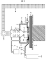
- FIG. 1 is an entire configuration diagram of a charged particle beam device of a first embodiment.
- FIG. 7 is an entire configuration diagram of a charged particle beam device of Example 2; 6 shows a configuration example of an operation screen used in the charged particle beam device of the second embodiment. 6 shows a configuration example of an operation screen used in the charged particle beam device of the second embodiment.
- FIG. 8 is an entire configuration diagram of a charged particle beam device of a third embodiment.
- FIG. 8 is an entire configuration diagram of a charged particle beam device of a fourth embodiment. 11 shows a modification of the charged particle beam device of Example 4.
- FIG. 14 is an entire configuration diagram of a charged particle beam device of a fifth embodiment.
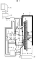
- the whole block diagram of the charged particle apparatus of a present Example is shown in FIG.
- the apparatus shown in FIG. 1 is a scanning type microscope which scans a charged particle beam onto a sample 6 to detect and image secondary electrons or reflected electrons obtained, and roughly an electron optical lens barrel 2 ,
- a first case 7 for supporting the electron optical lens barrel 2 a second case 8 for storing a sample to be observed, a thin film for transmitting a primary electron beam provided on the lower surface of the first case 7 It consists of ten.
- the electron optical lens barrel 2 is disposed so as to protrude inside the first housing 7, and at the end of the electron optical lens barrel 2, a detector 3 for detecting the secondary electrons or reflected electrons is disposed. .
- the detector 3 is provided inside the first housing 7 but may be disposed inside the electron optical lens barrel 2 or inside the second housing 8.
- a through hole for transmitting the primary electron beam may be provided on the bottom surface of the first housing 7.
- the alternate long and short dash line in the figure indicates the primary electron beam optical axis, and the electron optical lens barrel 2, the first housing 7 and the thin film 10 are assembled coaxially with the primary electron beam optical axis.
- control of the vacuum exhaust system and the electron optical system is performed in accordance with commands transmitted from the personal computer 35 used by the apparatus user and the host control unit 36 connected with the personal computer 35 to perform communication and the host control unit 36
- the lower control unit 37 is provided.
- the personal computer 35 includes a monitor on which an operation screen (GUI) of the apparatus is displayed, and an input unit to an operation screen such as a keyboard or a mouse.
- GUI operation screen
- the upper control unit 36, the lower control unit 37, and the personal computer 35 are connected by communication lines 43 and 44, respectively.
- the lower control position unit 37 is a unit for transmitting and receiving control signals for controlling the vacuum exhaust pump 4, the gas control valve 101, the electron source 0, the optical lens 1 and the like, and further the output signal of the detector 3 is a digital image signal And transmit to the upper control unit 36.
- the upper control unit 36 and the lower control unit 37 may be mixed with analog circuits and digital circuits, and the upper control unit 36 and the lower control unit 37 may be unified into one.
- the configuration of the control system shown in FIG. 1 is merely an example, and modifications of the control unit, the valve, the vacuum pump, and the wiring for communication, etc. may be the SEM of this embodiment as long as the functions intended in this embodiment are satisfied. And belongs to the category of charged particle beam devices.
- the electron optical lens barrel 2 stores an electron optical system inside, and the electron optical system deflects the orbits of the electron source 0 which emits the primary electron beam, the various optical lenses 1 which control the orbit of the electron beam, and the electron beam Is configured to include various deflectors and the like.
- the electron optical lens barrel 2 and the electron optical system also become a charged particle optical lens barrel and a charged particle optical system, and the electron source becomes an ion source.
- the various optical lenses and the various deflectors are composed of electrostatic lenses or electrostatic deflectors. In the case of an ion beam, mass separation occurs when using a magnetic lens and deflector.
- the interior of the electro-optical lens barrel 2 and the first housing 7 (strictly, the closed space formed by the surface of the first housing 7 and the surface of the electro-optical lens barrel 2) 4.
- the vacuum pump is evacuated to maintain the pressure lower than the atmospheric pressure.
- a vacuum sealing member 17 is provided at the junction of the first housing 7 with the electron optical lens barrel 2.
- the second housing 8 is provided with an opening 81 (or an opening surface) for opening the inside to the atmosphere, and the inside is always kept open to the atmosphere during observation of the sample.
- first space 12 the spaces inside the second housing 8 and the first housing 7 may be referred to as a first space 12 and a second space 11, respectively.
- the second space 11 includes the passage of the primary electron beam before passing through the thin film
- the first space 12 includes the passage of the primary electron beam after passing through the thin film 10.
- one vacuum evacuation pump 4 evacuates the inside of the electron optical lens barrel 2 and the inside of the first housing 7
- two or more vacuum pumps are provided to set the electron optical lens barrel 2 and the first
- the housing 7 may be evacuated independently.
- the pipe 16 is connected to both the electron optical lens barrel 2 and the first housing, it may be connected by separate pipes.
- the first case is provided with the leak valve 15 and the inside of the first case 7 is opened to the atmosphere when the apparatus is stopped, but the installation location in the first case 7 is not particularly limited. Further, two or more leak valves 15 may be provided, and furthermore, they may not necessarily be provided.
- the area of the through hole is preferably 1 mm 2 or less. This is because the area of the through hole needs to be about 1 mm 2 or less in order to realize differential pumping with a vacuum pump that can be practically used, such as a turbo molecular pump or a rotary pump. Since the second housing 8 and the first housing are differentially discharged, it is better to provide a vacuum pump for exhausting the inside of the electron optical lens barrel 2 and the first housing independently.
- the thickness of a thin film needs to be 20 micrometers or less.
- the thickness through which the electron beam passes is about 20 ⁇ m.
- the sample 6 is placed on the sample table 501 and stored in the second housing 8.
- the sample stand 501 is prepared in various thicknesses, and an appropriate sample stand is selected according to the thickness of the observation sample and stored in the second housing 8. Although this operation needs to be performed manually, the distance between the thin film 10 and the surface of the observation sample can be adjusted to an appropriate size.
- the second case 8 is provided with the opening 81, even a large-sized sample which is protruded from the case as shown in FIG. 1 can be placed in the case.
- the inside of the second housing 8 is always open to the atmosphere, it is possible to insert a hand into the inside of the housing from the opening 81 even during SEM observation, and by moving the sample table 501 It is possible to change the observation position of the sample 6 during the SEM observation.
- an atmospheric pressure SEM can be realized which can observe even a large sample that can not fit in the vacuum second housing of a normal SEM.
- an SEM or charged particle beam apparatus capable of changing the observation position of the sample without changing the transmission position of the charged particle beam.
- the distance between the sample and the thin film is preferably as short as possible, but on the other hand, if the distance between the thin film and the sample is too short, the thin film may be damaged.
- the distance between the sample and the thin film is adjusted by the thickness of the sample table 501 disposed in the second housing.
- the distance between the sample and the thin film is adjusted by the thickness of the sample table 501 disposed in the second housing.
- FIG. 2 shows the entire configuration of the charged particle device of this embodiment. Since the apparatus configuration shown in FIG. 2 has many parts in common with the apparatus configuration shown in FIG. 1, the description of the common parts will be omitted, and only differences will be described.
- the SEM shown in FIG. 2 includes an electron optical barrel 2, a first case 7 supporting the electron optical barrel 2, a second case 8 in which a sample to be observed is stored, and FIG.
- the thin film 10 is attached to the lower surface of the first housing 7 via the thin film support member 47.
- any means may be used as long as vacuum sealing is possible.
- a vacuum sealing member such as an O-ring may be used, or an organic material such as an adhesive or a tape may be used.
- the thin film 10 may be replaced by a suitable plate member having an open through hole.
- An annular opening is provided on the lower surface of the first housing 7, and the thin film support member 47 is attached from the outside of the first housing 7 so as to cover the opening.
- the first housing 7 and the electro-optical lens barrel 2 are evacuated by the vacuum evacuation pump 4, but the vacuum seal of the first housing 7 is maintained by the O-ring provided at the outer edge of the opening. Therefore, the thin film support member 47 is detachable with respect to the first housing 7.
- the thin film 10 is very thin and is very difficult to handle. Therefore, by attaching the thin film 10 to the thin film support member 47 outside the apparatus, the thin film support member 47 provided with the thin film 10 is attached to the first housing 7, which makes the replacement very easy. That is, if the thin film 10 is broken, it is configured to be replaced together with the thin film support member 47.
- the SEM of the present embodiment is provided with a sample stage for holding the observation target sample in the second housing 8 and performing position driving.
- the sample stage includes a sample stage 5 on which the sample 6 is placed, a Z drive mechanism 502, and an XY drive mechanism 503.
- the sample 6 is carried into the second housing 8 from the opening 81.
- the second housing 8 is provided with a position measuring device 14 and can detect the height of the sample surface and the position in the in-plane direction.
- an optical distance meter can be used as the position measuring device 14.
- the measurement result of the position measurement device 14 is transmitted to the personal computer 35 via the lower control unit 37 and the upper control unit 36 and displayed on the monitor.
- the apparatus user operates the Z drive mechanism 502 while watching the measurement result displayed on the monitor, and brings the sample 6 close to the thin film 10 to such an extent that the sample surface does not contact the thin film 10.
- the SEM shown in FIG. 2 shows a configuration in which the Z drive mechanism 502 is moved by a manual operation, a motor or an actuator can be attached to the Z drive mechanism 502, and the movement amount of the Z drive mechanism 502 can be manipulated by GUI on the monitor. It is also possible to configure the device.
- the SEM of this embodiment includes a gas nozzle 100 capable of releasing a gas lighter in mass than the atmosphere to the vicinity of the primary electron beam irradiation position of the sample.
- the gas nozzle 100 is connected to a gas cylinder 103 filled with the light element gas via a pipe.
- a gas control valve 101, a junction 102 and the like are provided in the middle of the piping.
- the gas cylinder 103 is not a component of the SEM but is connected after the user of the apparatus, but may be sold as it is incorporated in the apparatus of the SEM.
- the primary electron beam that has passed through the thin film 10 or the through hole penetrates into the second housing 8, but the inside of the second housing 8 is maintained at atmospheric pressure or a low vacuum state. Therefore, the intruded primary electron beam is scattered by gas molecules such as nitrogen and oxygen, and the mean free path becomes shorter than that in the first case 7. If the mean free path is shorter than the distance between the thin film 10 and the surface of the sample 6, the electron beam can not reach the sample and SEM observation can not be performed.
- the mean free path of the electron beam becomes shorter as the mass of the gas molecule which is the scattering cause increases. Therefore, if the passage path of the primary electron beam in the second housing 8 is filled with gas molecules whose mass is lighter than nitrogen or oxygen which is the main element constituting the atmosphere, the mean free path is made longer than the atmospheric atmosphere. Can. Therefore, the SEM of the present embodiment is provided with the gas nozzle 100, and emits light element gas such as hydrogen gas, helium gas, methane gas, water vapor and the like near the primary electron beam irradiation position of the sample.
- light element gas such as hydrogen gas, helium gas, methane gas, water vapor and the like
- This increases the probability that the primary electron beam that has penetrated into the second housing 8 reaches the sample, thus increasing the amount of reflected electrons or secondary electrons emitted from the sample and reflecting electrons or secondary electrons. Can be reduced in the second housing 8. As a result, the probability that the backscattered electrons or secondary electrons reach the detector 3 becomes high, and the image quality of the acquired SEM image is improved.
- the SEM of the present embodiment is provided with an EDX detector 18 in the first housing 7 so that material analysis of the observation sample can be performed.
- a detector for fluorescent light may be provided.
- an absorption current flows in the sample. If the current flowing from the sample 6 to the sample table is measured, it is also possible to obtain an image using the absorbed current (or absorbed electrons).
- an ammeter is provided in the lower control unit 37, and the sample mounting surface of the sample stand 5 is made of a conductive material so that the sample stand 5 has a current detection function.
- an operation window 50 for example, an operation window 50, an image display unit 51, an image observation start button 52 for starting emission of an electron beam and starting image display, and stop emission of an electron beam
- the image observation stop button 53 for stopping the display
- the focus adjustment button 54 for adjusting the optical lens such as the deflection lens and the objective lens to execute autofocus
- the brightness adjustment button 55 for adjusting the brightness of the image
- the contrast Atmospheric leak for making the inside of the contrast adjustment button 56 for adjustment
- the evacuation button 57 for starting evacuation of the inside of the charged particle optical lens barrel 2 and the first casing 7, and the inside of the first casing 7 atmospheric leak
- a button 58 for example, an operation window 50, an image display unit 51, an image observation start button 52 for starting emission of an electron beam and starting image display, and stop emission of an electron beam
- the image observation stop button 53 for stopping the display
- the focus adjustment button 54 for adjusting the optical lens such as the deflection lens and the objective lens to execute autofocus
- the brightness adjustment button 55 for adjusting
- evacuation button 57 When the evacuation button 57 is clicked on the screen, evacuation is started, and when it is clicked again, evacuation is stopped.
- evacuation button 58 The same applies to the operation of the atmospheric leak button 58.
- the processing executed by the above button operation can also be executed by operating a mechanical button or knob attached to the device body.
- the operation window 50 has a gas release start button 112 for releasing the gas from the gas nozzle by opening the gas control valve 101, and a gas release stop button 113 for closing the gas control valve 101 to stop the gas release.
- the gas release stop button 113 is forgotten and the gas control valve 101 may be opened and the gas cylinder 103 may become empty.
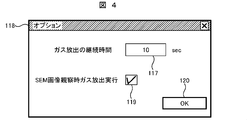
- the gas release condition setting button 114 shown in FIG. 3 is pressed, the gas release condition setting window 118 shown in FIG. 4 is opened, and it is possible to set gas release conditions such as whether or not to execute gas release or duration of gas release. Become.
- a time for which gas release is to be continued is input in the gas release time setting box displayed in the window, after clicking on the gas release start button 112, the gas release continues for the entered time, and is automatically stopped after the time has elapsed.
- the duration of gas release is not set in another window as shown in FIG. 4, but is stored as a fixed value in the upper control unit 36 or the lower control unit 37 and after the gas release start button 112 is clicked.
- the apparatus may be configured to forcibly stop the gas release after a predetermined time has elapsed.
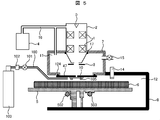
- FIG. 5 is a schematic view showing the configuration of the SEM of this example. Although the control system is omitted for the sake of simplicity, in practice, as in FIGS. 1 and 2, control means is provided to control the electron optical system and the vacuum exhaust system.
- the distance between the thin film and the sample is desirably as short as possible regardless of the atmosphere in the passage of the primary electron beam, but on the other hand, if the thin film and the sample come close to each other, the thin film is more likely to be damaged. This problem is particularly serious when using a thin film that transmits an electron beam.
- a limiting member 105 for preventing the thin film from contacting the sample as shown in FIG.
- the limiting member 105 any member capable of limiting the distance between the sample and the thin film may be used, but for convenience, an adhesive or a tape is attached to the sample facing surface side of the thin film 10 to form the limiting member 105. It can also be used. However, in consideration of the mean free path of the primary electron beam that has passed through the thin film 10, it is preferable that the limiting member 105 be made of a thin film material whose thickness is accurately known. Further, although the limiting member 105 is attached to the thin film 10 in FIG. 5, the limiting member 105 may be attached to the thin film support member 47 or the sample stand 5 or may be placed on the sample 6. Furthermore, the restriction member 105 may be removable.
- the limiting member 105 is configured to be removable.
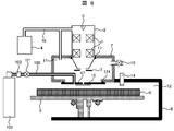
- FIG. 6 shows the entire structure of the SEM of this embodiment. Similar to FIG. 5, various control systems are omitted.
- the drive mechanism 200 is provided on the upper portion of the electron optical lens barrel 2, and the thin film is obtained by moving the entire electron optical lens barrel 2 and the first housing 7 in the vertical direction. The relative distance between 10 and the sample 6 placed on the sample table 21 is adjusted.
- a limiting member 105 is provided on the sample facing surface side of the thin film 10, and a position measuring device 14 is provided on a flange portion 19 protruding from the bottom of the first housing 7.
- the thin film 10 is attached to the thin film support member 47 and is configured to be removable from the first housing 7.
- the vacuum pump 4 and the pipe 16 are also moved in conjunction with the electron optical lens barrel 2 and the first housing 7, but the pipe 16 and the electron optical lens barrel 2 and the first housing 7
- a sliding member having a vacuum seal property may be provided between the two so that the vacuum pump 4 and the pipe 16 do not move when the drive mechanism 200 is operated.
- the electron optical lens barrel 2 and the first housing 7 are supported by the support column 20, the electron optical lens barrel 2 and the first housing 7 are functional members supporting the entire apparatus including the electron optical lens barrel 2 and the first housing 7.
- the second case is unnecessary. Therefore, the SEM of the structure of the present example is particularly suitable for observation as it is without cutting a large sample. Alternatively, it is suitable when having a very large sample stage such as a belt conveyor.
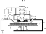
- FIG. 7 shows still another modified example of the SEM provided with a mechanism for changing the distance between the thin film and the sample.
- the thin film support member 47 is made slidable with respect to the first housing 7, and the thin film support member 47 is made movable by the drive mechanism 201.
- the vacuum seal between the thin film support member 47 and the first housing 7 is realized by the vacuum sealing mechanism 124, but the vacuum sealing mechanism 124 needs to have slidability.
- the SEM shown in FIG. 7 can adjust the distance between the thin film and the sample by both the Z drive mechanism 502 and the drive mechanism 201.
- the Z drive mechanism 502 may be used, and when it is to be finely performed, the drive mechanism 201 may be used.
- the sample When it is desired to shorten the distance from the objective lens of the SEM to the sample, ie, the focal length, the sample is brought close to the thin film 10 by the Z drive mechanism 502, and when the focal length is desired to be long, the thin film 10 is brought close to the sample And so on.
- a drive mechanism 201 for driving the thin film side as shown in FIG. 7 is very useful.
- the sample 6 is very large and the device shown in FIG. 7 is a very small device, it may be very difficult to move the sample 6 itself, in which case the position of the sample 6 is fixed It is desirable to drive the thin film side to bring the thin film 10 closer to the sample.
- FIG. 8 shows a modification of the arrangement of the gas nozzles for supplying the light element gas to the observation position.
- the gas nozzle 100 is disposed on the bottom of the first housing 7 and introduced from the side of the opening 81 of the second housing 8 or the bottom of the first housing 7.
- the present embodiment by introducing a pipe into the first housing 7 and inserting a nozzle into the thin film support member 47, light element gas is supplied to the sample surface from the thin film support member 47 side.
- it is possible to insert a gas nozzle into the thin film 10 itself it is better to insert the gas nozzle into the thin film support member 47 because there is a high possibility that the thin film 10 will be damaged when the thin film support member 47 is desorbed.
Abstract
Description
1 光学レンズ
2 電子光学鏡筒
3 検出器
4 真空排気ポンプ
5,21 試料台
6 試料
7 第1の筐体
8 第2の筐体
10 薄膜
11 第2の空間
12 第1の空間
14 位置測定器
15 リークバルブ
16 配管
17 真空封止部
18 EDX検出器
19 フランジ部
20 支柱
35 パソコン
36 上位制御部
37 下位制御部
43,44 通信線
47 薄膜支持部材
50 操作用ウィンドウ
51 画像表示部
52 画像観察開始ボタン
53 画像観察停止ボタン
54 焦点調整ボタン
55 明るさ調整ボタン
56 コントラスト調整ボタン
57 真空排気ボタン
58 大気リークボタン
81 開口部
101 ガス制御バルブ
103 ガスボンベ
112 ガス放出開始ボタン
113 ガス放出停止ボタン
114 ガス放出条件設定ボタン
117 ガス放出時間設定ボックス
118 ガス放出条件設定ウィンドウ
119 ガス放出実行チェックボックス
120 OKボタン
124 真空封止機構 0 electron source 1
Claims (19)
- 荷電粒子源から放出される一次荷電粒子線を試料上に走査する荷電粒子光学系と、当該荷電粒子光学系を格納する荷電粒子光学鏡筒と、前記走査により得られる反射電子あるいは二次電子を検出する検出器と、少なくとも一つ以上の排気ポンプとを含む荷電粒子線装置において、
前記試料を格納し、前記荷電粒子線装置全体を装置設置面に対して支持する第2の筐体と、
当該第2の筐体上に設けられ、前記荷電粒子光学鏡筒を支持する第1の筐体と、
前記第1の筐体の底面に設けられる、前記一次荷電粒子線を透過あるいは通過させる薄膜とを備え、
装置動作時に、前記荷電粒子光学鏡筒,前記第1の筐体および前記薄膜によって囲まれる閉空間内が真空排気され、
前記第2の筐体が大気開放されることを特徴とする荷電粒子線装置。 A charged particle optical system for scanning a primary charged particle beam emitted from a charged particle source onto a sample, a charged particle optical lens barrel for storing the charged particle optical system, and reflected electrons or secondary electrons obtained by the scanning In a charged particle beam device including a detector for detection and at least one exhaust pump,
A second housing for storing the sample and supporting the entire charged particle beam device with respect to the device mounting surface;
A first case provided on the second case and supporting the charged particle optical lens barrel;
And a thin film which is provided on the bottom of the first case and transmits or passes through the primary charged particle beam.
During operation of the apparatus, the inside of a closed space surrounded by the charged particle optical lens barrel, the first housing, and the thin film is evacuated.
A charged particle beam device characterized in that the second case is opened to the atmosphere. - 荷電粒子源から放出される一次荷電粒子線を試料上に走査する荷電粒子光学系と、当該荷電粒子光学系を格納する荷電粒子光学鏡筒と、前記走査により得られる反射電子あるいは二次電子を検出する検出器と、少なくとも一つ以上の排気ポンプとを含む荷電粒子線装置において、
前記一次荷電粒子線の通過経路上に配置される、前記一次荷電粒子線を透過あるいは通過させる薄膜と、
当該薄膜を保持する薄膜支持部材と、
前記試料を格納し、前記荷電粒子線装置全体を装置設置面に対して支持する第2の筐体と、
当該第2の筐体上に配置され、前記薄膜支持部材および前記荷電粒子光学鏡筒とを一定距離離間させるように支持する第1の筐体と、
装置動作時に、前記荷電粒子光学鏡筒,前記薄膜支持部材および前記第1の筐体によって構成される閉空間が真空排気され、
前記第2の筐体が大気開放されることを特徴とする荷電粒子線装置。 A charged particle optical system for scanning a primary charged particle beam emitted from a charged particle source onto a sample, a charged particle optical lens barrel for storing the charged particle optical system, and reflected electrons or secondary electrons obtained by the scanning In a charged particle beam device including a detector for detection and at least one exhaust pump,
A thin film for transmitting or passing the primary charged particle beam, which is disposed on a passage of the primary charged particle beam;
A thin film support member for holding the thin film;
A second housing for storing the sample and supporting the entire charged particle beam device with respect to the device mounting surface;
A first case disposed on the second case and supporting the thin film support member and the charged particle optical lens barrel so as to be separated by a predetermined distance;
During operation of the apparatus, a closed space constituted by the charged particle optical lens barrel, the thin film support member and the first casing is evacuated.
A charged particle beam device characterized in that the second case is opened to the atmosphere. - 荷電粒子源から放出される一次荷電粒子線を試料上に走査する荷電粒子光学系と、当該荷電粒子光学系を格納する荷電粒子光学鏡筒と、前記走査により得られる反射電子あるいは二次電子を検出する検出器と、少なくとも一つ以上の排気ポンプとを含む荷電粒子線装置において、
前記一次荷電粒子線を透過あるいは透過させる薄膜および当該薄膜を保持する薄膜支持部材と、
前記試料を格納し、かつ内部が常時大気開放される第2の筐体と、
当該第2の筐体の上部に設置され、内部が真空排気される第1の筐体とを備え、
前記検出器は、前記薄膜を通過して当該薄膜の上方に到達する二次電子あるいは反射電子を検出することを特徴とする荷電粒子線装置。 A charged particle optical system for scanning a primary charged particle beam emitted from a charged particle source onto a sample, a charged particle optical lens barrel for storing the charged particle optical system, and reflected electrons or secondary electrons obtained by the scanning In a charged particle beam device including a detector for detection and at least one exhaust pump,
A thin film which transmits or transmits the primary charged particle beam, and a thin film supporting member for holding the thin film,
A second case for storing the sample and in which the inside is always open to the atmosphere;
And a first case installed at the top of the second case and evacuated inside.
The charged particle beam device, wherein the detector detects secondary electrons or reflected electrons that pass through the thin film and reach above the thin film. - 請求項2または3に記載の荷電粒子線装置において、
前記第2の筐体内にガスを供給するガスノズルを備え、当該ガスノズルにより大気よりも質量の軽いガスが前記第1の筐体内に供給されることを特徴とする荷電粒子線装置。 In the charged particle beam device according to claim 2 or 3,
A charged particle beam apparatus, comprising: a gas nozzle for supplying a gas into the second housing, wherein a gas whose mass is lighter than the atmosphere is supplied into the first housing by the gas nozzle. - 請求項4に記載の荷電粒子線装置において、
前記ガスノズルからの放出ガスが、水素ガス,ヘリウムガス,メタンガス,水蒸気の内いずれかを含むことを特徴とする荷電粒子線装置。 In the charged particle beam device according to claim 4,
A charged particle beam device characterized in that the gas released from the gas nozzle contains any one of hydrogen gas, helium gas, methane gas and water vapor. - 請求項4に記載の荷電粒子線装置において、
前記ガスノズルが、前記薄膜支持部材に取り付けられていることを特徴とする荷電粒子線装置。 In the charged particle beam device according to claim 4,
The charged particle beam device, wherein the gas nozzle is attached to the thin film support member. - 請求項2または3に記載の荷電粒子線装置において、
前記薄膜支持部材は、前記第1の筐体に対して着脱可能であることを特徴とする荷電粒子線装置。 In the charged particle beam device according to claim 2 or 3,
The charged particle beam device, wherein the thin film support member is attachable to and detachable from the first case. - 請求項2または3に記載の荷電粒子線装置において、
前記第2の筐体に、前記薄膜と前記試料との距離を計測する計測手段を備えたことを特徴とする荷電粒子線装置。 In the charged particle beam device according to claim 2 or 3,
A charged particle beam apparatus, comprising: measuring means for measuring a distance between the thin film and the sample in the second case. - 請求項2または3に記載の荷電粒子線装置において、
前記第2の筐体内に、前記試料を載置する試料台と、当該試料台をZ方向に移動させるZステージとを備えたことを特徴とする荷電粒子線装置。 In the charged particle beam device according to claim 2 or 3,
A charged particle beam apparatus, comprising: a sample stage on which the sample is placed; and a Z stage for moving the sample stage in the Z direction in the second housing. - 請求項2または3に記載の荷電粒子線装置において、
前記薄膜または薄膜支持部材が、前記試料と前記薄膜との距離を制限する制限部材を備えることを特徴とする荷電粒子線装置。 In the charged particle beam device according to claim 2 or 3,
The charged particle beam device, wherein the thin film or the thin film support member includes a limiting member that limits the distance between the sample and the thin film. - 請求項2または3に記載の荷電粒子線装置において、
少なくとも前記第2の筐体または第1の筐体のいずれかに、前記一次荷電粒子線の照射に伴い前記試料から放出されるイオン,荷電粒子,光子,X線のいずれか一つ以上を検出する第2の検出器を備えることを特徴とする荷電粒子線装置。 In the charged particle beam device according to claim 2 or 3,
At least one of the second housing or the first housing detects at least one of ions, charged particles, photons, and X-rays emitted from the sample as the primary charged particle beam is irradiated. What is claimed is: 1. A charged particle beam device comprising a second detector. - 請求項2または3に記載の荷電粒子線装置において、
前記第1の筐体内に、前記一次荷電粒子線の照射により試料に流れ込む荷電粒子または電流を検出する機能を備えた試料台を備えることを特徴とする荷電粒子線装置。 In the charged particle beam device according to claim 2 or 3,
A charged particle beam apparatus comprising a sample stage provided with a function of detecting charged particles or current flowing into a sample by irradiation of the primary charged particle beam in the first case. - 請求項4に記載の荷電粒子線装置において、
前記ガスノズルからのガスの放出状態を制御する制御手段と、
当該制御手段を操作するための操作画面が表示されるモニタとを有することを特徴とする荷電粒子線装置。 In the charged particle beam device according to claim 4,
Control means for controlling the discharge state of the gas from the gas nozzle;
And a monitor on which an operation screen for operating the control means is displayed. - 請求項13に記載の荷電粒子線装置において、
前記操作画面上に、前記ガスの放出開始,停止あるいはガス放出の継続時間を入力するボタンあるいは入力ボックスが表示されることを特徴とする荷電粒子線装置。 In the charged particle beam device according to claim 13,
A charged particle beam device characterized in that a button or an input box for inputting a release start or stop of the gas or a continuation time of the gas release is displayed on the operation screen. - 請求項1に記載の荷電粒子線装置において、
前記薄膜の厚みが20μm以下であることを特徴とする荷電粒子線装置。 In the charged particle beam device according to claim 1,
The charged particle beam device, wherein a thickness of the thin film is 20 μm or less. - 請求項1に記載の荷電粒子線装置において、
前記薄膜が、前記一次荷電粒子線が通過するための、面積1mm2以下の貫通孔を備えることを特徴とする荷電粒子線装置。 In the charged particle beam device according to claim 1,
A charged particle beam device characterized in that the thin film is provided with a through hole having an area of 1 mm 2 or less for the primary charged particle beam to pass through. - 荷電粒子光学鏡筒の端部より出射する一次荷電粒子線を試料上に走査し、当該走査により得られる反射電子あるいは二次電子を画像化して前記試料を観察する顕微方法において、
前記荷電粒子光学鏡筒の端部と離間されて配置された前記一次荷電粒子線を透過あるいは通過させる薄膜と前記端部との間に存在する一次荷電粒子線の第1の通過経路を真空状態に維持し、
前記薄膜と前記試料間に存在する一次荷電粒子線の第2の通過経路に大気よりも質量の軽いガスを供給し、
前記走査により得られる二次電子または反射電子のうち前記薄膜を透過あるいは通過して前記荷電粒子光学鏡筒側に戻ってくる二次電子または反射電子を検出することにより、前記試料の観察を行うことを特徴とする顕微方法。 In a microscopic method, a primary charged particle beam emitted from an end of a charged particle optical column is scanned on a sample, and reflected electrons or secondary electrons obtained by the scan are imaged to observe the sample,
The first passage path of the primary charged particle beam existing between the end portion and the thin film for transmitting or passing the primary charged particle beam spaced apart from the end portion of the charged particle optical lens barrel is evacuated To maintain
Supplying a gas lighter in mass than the atmosphere to a second passage of the primary charged particle beam existing between the thin film and the sample;
The sample is observed by detecting secondary electrons or reflected electrons among the secondary electrons or reflected electrons obtained by the scanning, which are transmitted or passed through the thin film and returned to the charged particle optical lens barrel side. A microscopic method characterized by - 請求項17に記載の顕微方法において、
前記第2の通過経路の長さを所定の長さに調整して、前記試料の観察を行うことを特徴とする顕微方法。 In the microscopic method according to claim 17,
A microscopic method comprising observing the sample by adjusting the length of the second passage to a predetermined length. - 請求項17に記載の顕微方法において、
前記大気よりも質量の軽いガスが、水素ガス,ヘリウムガス,メタンガス,水蒸気のいずれか一つを含むこと特徴とする顕微方法。 In the microscopic method according to claim 17,
The microscopic method characterized in that the gas lighter in mass than the atmosphere contains any one of hydrogen gas, helium gas, methane gas, and water vapor.
Priority Applications (6)
| Application Number | Priority Date | Filing Date | Title |
|---|---|---|---|
| KR1020137027846A KR101390112B1 (en) | 2011-01-31 | 2011-11-02 | Charged particle beam apparatus |
| DE112011104347.3T DE112011104347B4 (en) | 2011-01-31 | 2011-11-02 | Device and microscopy method with a charged particle beam |
| KR1020137020260A KR101389660B1 (en) | 2011-01-31 | 2011-11-02 | Charged particle beam apparatus |
| CN201180066230.2A CN103329240B (en) | 2011-01-31 | 2011-11-02 | Charged particle beam apparatus |
| KR1020147005627A KR101514190B1 (en) | 2011-01-31 | 2011-11-02 | Charged particle beam apparatus |
| US13/982,805 US9543111B2 (en) | 2011-01-31 | 2011-11-02 | Charged particle beam device |
Applications Claiming Priority (2)
| Application Number | Priority Date | Filing Date | Title |
|---|---|---|---|
| JP2011017383A JP5320418B2 (en) | 2011-01-31 | 2011-01-31 | Charged particle beam equipment |
| JP2011-017383 | 2011-01-31 |
Publications (1)
| Publication Number | Publication Date |
|---|---|
| WO2012104942A1 true WO2012104942A1 (en) | 2012-08-09 |
Family
ID=46602190
Family Applications (1)
| Application Number | Title | Priority Date | Filing Date |
|---|---|---|---|
| PCT/JP2011/006127 WO2012104942A1 (en) | 2011-01-31 | 2011-11-02 | Charged particle beam apparatus |
Country Status (6)
| Country | Link |
|---|---|
| US (1) | US9543111B2 (en) |
| JP (1) | JP5320418B2 (en) |
| KR (3) | KR101389660B1 (en) |
| CN (2) | CN104851769A (en) |
| DE (1) | DE112011104347B4 (en) |
| WO (1) | WO2012104942A1 (en) |
Cited By (8)
| Publication number | Priority date | Publication date | Assignee | Title |
|---|---|---|---|---|
| WO2014030435A1 (en) * | 2012-08-24 | 2014-02-27 | 株式会社 日立ハイテクノロジーズ | Observation device and light axis adjustment method |
| WO2014030430A1 (en) * | 2012-08-20 | 2014-02-27 | 株式会社 日立ハイテクノロジーズ | Charged particle beam device and sample observation method |
| WO2014038287A1 (en) * | 2012-09-05 | 2014-03-13 | 株式会社日立ハイテクノロジーズ | Member for charged particle beam devices, charged particle beam device, and diaphragm member |
| WO2014041876A1 (en) * | 2012-09-14 | 2014-03-20 | 株式会社 日立ハイテクノロジーズ | Charged particle beam device and sample observation method |
| JP2014056785A (en) * | 2012-09-14 | 2014-03-27 | Hitachi High-Technologies Corp | Charged particle beam device and sample observation method |
| WO2014050242A1 (en) * | 2012-09-27 | 2014-04-03 | 株式会社 日立ハイテクノロジーズ | Charged particle radiation device |
| JP2014060145A (en) * | 2012-08-21 | 2014-04-03 | B-Nano Ltd | Electron microscope imaging system and method |
| CN105493224A (en) * | 2013-08-23 | 2016-04-13 | 株式会社日立高新技术 | Diaphragm mounting member and charged particle beam device |
Families Citing this family (23)
| Publication number | Priority date | Publication date | Assignee | Title |
|---|---|---|---|---|
| JP6207824B2 (en) * | 2012-10-01 | 2017-10-04 | 株式会社日立ハイテクノロジーズ | Charged particle beam apparatus, diaphragm position adjustment method, and diaphragm position adjustment jig |
| JP6051014B2 (en) | 2012-10-29 | 2016-12-21 | 株式会社日立ハイテクノロジーズ | Sample storage container, charged particle beam apparatus, and image acquisition method |
| JP6362827B2 (en) * | 2013-01-26 | 2018-07-25 | 株式会社ホロン | Alignment measuring apparatus and alignment measuring method |
| JP6309195B2 (en) * | 2013-02-18 | 2018-04-11 | 株式会社ホロン | Scanning electron microscope and inspection device |
| KR102026936B1 (en) * | 2013-03-26 | 2019-10-01 | 삼성디스플레이 주식회사 | Inspection system using scanning electron microscope |
| US9741526B2 (en) * | 2013-09-06 | 2017-08-22 | Hitachi High-Technologies Corporation | Charged particle beam apparatus and sample image acquiring method |
| JP6117070B2 (en) * | 2013-09-26 | 2017-04-19 | 株式会社日立ハイテクノロジーズ | electronic microscope |
| JP6047508B2 (en) | 2014-01-27 | 2016-12-21 | 株式会社日立ハイテクノロジーズ | Charged particle beam apparatus, sample image acquisition method, and program recording medium |
| JP6302702B2 (en) * | 2014-02-27 | 2018-03-28 | 株式会社日立ハイテクノロジーズ | Scanning electron microscope and image generation method |
| JP6199333B2 (en) * | 2015-04-03 | 2017-09-20 | 株式会社 テクネックス工房 | Scanning electron microscope |
| JP6973072B2 (en) * | 2015-06-08 | 2021-11-24 | 株式会社ニコン | Charged particle beam irradiator |
| DE112015006731B4 (en) * | 2015-08-21 | 2022-07-28 | Hitachi High-Tech Corporation | VIEW SUPPORT UNIT FOR CHARGE PARTICLE MICROSCOPE AS WELL AS CHARGE PARTICLE MICROSCOPE AND SAMPLE VIEWING METHOD USING THIS |
| JP6118870B2 (en) * | 2015-10-07 | 2017-04-19 | 株式会社日立ハイテクノロジーズ | Sample observation method |
| KR101725139B1 (en) * | 2015-11-20 | 2017-04-10 | 한국표준과학연구원 | Electron microscope comprising multie-holder arranged sample-stage |
| CN107437487A (en) * | 2016-05-25 | 2017-12-05 | 宝山钢铁股份有限公司 | One kind is used for sample platform of scanning electronic microscope lifting anticollision device, collision-prevention device |
| US10607808B2 (en) | 2017-09-13 | 2020-03-31 | Taiwan Electron Microscope Instrument Corporation | Examination container and electron microscope |
| CN110186944B (en) * | 2018-02-23 | 2021-11-09 | 台湾电镜仪器股份有限公司 | Inspection container and electron microscope |
| CN110186942A (en) * | 2018-02-23 | 2019-08-30 | 台湾电镜仪器股份有限公司 | Film assembly examines container and electron microscope |
| US10593513B2 (en) | 2018-07-18 | 2020-03-17 | Taiwan Electron Microscope Instrument Corporation | Membrane assembly, examination container and electron microscope |
| JP2020017415A (en) * | 2018-07-26 | 2020-01-30 | 株式会社日立ハイテクノロジーズ | Charged particle beam device |
| KR102181455B1 (en) * | 2018-12-28 | 2020-11-23 | 참엔지니어링(주) | Apparatus and method for observing specimen |
| JP7091263B2 (en) * | 2019-01-22 | 2022-06-27 | 株式会社日立ハイテク | Depth calculation method for electron microscope and 3D structure |
| KR102180979B1 (en) * | 2019-08-19 | 2020-11-19 | 참엔지니어링(주) | Processing apparatus and method |
Citations (3)
| Publication number | Priority date | Publication date | Assignee | Title |
|---|---|---|---|---|
| JPH05234552A (en) * | 1992-02-21 | 1993-09-10 | Elionix Kk | Scanning electron microscope |
| JP2006147430A (en) * | 2004-11-22 | 2006-06-08 | Hokkaido Univ | Electron microscope |
| JP2008210765A (en) * | 2007-01-31 | 2008-09-11 | Jeol Ltd | Specimen holder, specimen inspection device, specimen inspection method, and method for manufacturing specimen holder |
Family Cites Families (24)
| Publication number | Priority date | Publication date | Assignee | Title |
|---|---|---|---|---|
| JPS522785A (en) * | 1975-06-24 | 1977-01-10 | Shimadzu Corp | Analyzing method and its device for the same |
| US4607167A (en) | 1982-10-19 | 1986-08-19 | Varian Associates, Inc. | Charged particle beam lithography machine incorporating localized vacuum envelope |
| EP0109147A3 (en) | 1982-10-19 | 1986-04-16 | Varian Associates, Inc. | Charged particle beam lithography machine incorporating localized vacuum envelope |
| JP2794471B2 (en) * | 1989-11-24 | 1998-09-03 | 日本電子テクニクス株式会社 | electronic microscope |
| JPH1064467A (en) | 1996-08-23 | 1998-03-06 | Toshiba Corp | Electron microscope |
| EP0969493A1 (en) * | 1998-07-03 | 2000-01-05 | ICT Integrated Circuit Testing Gesellschaft für Halbleiterprüftechnik mbH | Apparatus and method for examining specimen with a charged particle beam |
| JP2001008083A (en) | 1999-06-23 | 2001-01-12 | Seiji Ishikawa | Video microscope |
| JP2001242300A (en) | 2000-03-02 | 2001-09-07 | Sony Corp | Electron beam irradiation device |
| DE10032607B4 (en) | 2000-07-07 | 2004-08-12 | Leo Elektronenmikroskopie Gmbh | Particle beam device with a particle source to be operated in ultra-high vacuum and a cascade-shaped pump arrangement for such a particle beam device |
| JP3994759B2 (en) | 2002-03-07 | 2007-10-24 | ソニー株式会社 | Position control apparatus, position control method, and electron beam irradiation apparatus |
| JP2004354309A (en) | 2003-05-30 | 2004-12-16 | Mitsubishi Heavy Ind Ltd | Energy line extraction window, energy line projection device and energy line extraction method |
| JP2005108867A (en) | 2003-09-26 | 2005-04-21 | Tokyo Seimitsu Co Ltd | Exposure mask and electron beam exposure system |
| JP2005158338A (en) | 2003-11-21 | 2005-06-16 | Canon Inc | Observation device and machining device for sample |
| JP4262158B2 (en) * | 2004-07-13 | 2009-05-13 | 株式会社日立ハイテクサイエンスシステムズ | Low vacuum scanning electron microscope |
| JP2007188821A (en) * | 2006-01-16 | 2007-07-26 | Univ Osaka Sangyo | Handy electron microscope |
| JP2007294365A (en) * | 2006-04-27 | 2007-11-08 | Jeol Ltd | Test piece inspection method, test piece support body, and test piece inspection device as well as test piece inspection system |
| WO2008050321A2 (en) | 2006-10-24 | 2008-05-02 | B-Nano Ltd. | An interface, a methof for observing an object within a non-vacuum environment and a scanning electron microscope |
| DE102007021897A1 (en) | 2007-05-10 | 2008-11-20 | Fraunhofer-Gesellschaft zur Förderung der angewandten Forschung e.V. | Device for carrying out an electron beam process comprises a separating element which is fixed within a working chamber using detachable fixing elements |
| EP2061067A3 (en) | 2007-11-13 | 2010-04-07 | Carl Zeiss SMT Limited | Beam device and system comprising a particle beam device and an optical microscope |
| JP5253800B2 (en) * | 2007-12-26 | 2013-07-31 | 日本電子株式会社 | Sample holder, observation / inspection method, and observation / inspection apparatus |
| EP2105944A1 (en) * | 2008-03-28 | 2009-09-30 | FEI Company | Environmental cell for a particle-optical apparatus |
| JP2009277648A (en) * | 2008-04-17 | 2009-11-26 | Hitachi High-Technologies Corp | Inspection device and inspection method |
| US8334510B2 (en) * | 2008-07-03 | 2012-12-18 | B-Nano Ltd. | Scanning electron microscope, an interface and a method for observing an object within a non-vacuum environment |
| US8178851B2 (en) * | 2010-07-30 | 2012-05-15 | E.A. Fischione Instruments, Inc. | In situ holder assembly |
-
2011
- 2011-01-31 JP JP2011017383A patent/JP5320418B2/en not_active Expired - Fee Related
- 2011-11-02 KR KR1020137020260A patent/KR101389660B1/en active IP Right Grant
- 2011-11-02 KR KR1020147005627A patent/KR101514190B1/en active IP Right Grant
- 2011-11-02 KR KR1020137027846A patent/KR101390112B1/en active IP Right Grant
- 2011-11-02 CN CN201510171197.XA patent/CN104851769A/en active Pending
- 2011-11-02 CN CN201180066230.2A patent/CN103329240B/en not_active Expired - Fee Related
- 2011-11-02 US US13/982,805 patent/US9543111B2/en active Active
- 2011-11-02 WO PCT/JP2011/006127 patent/WO2012104942A1/en active Application Filing
- 2011-11-02 DE DE112011104347.3T patent/DE112011104347B4/en not_active Expired - Fee Related
Patent Citations (3)
| Publication number | Priority date | Publication date | Assignee | Title |
|---|---|---|---|---|
| JPH05234552A (en) * | 1992-02-21 | 1993-09-10 | Elionix Kk | Scanning electron microscope |
| JP2006147430A (en) * | 2004-11-22 | 2006-06-08 | Hokkaido Univ | Electron microscope |
| JP2008210765A (en) * | 2007-01-31 | 2008-09-11 | Jeol Ltd | Specimen holder, specimen inspection device, specimen inspection method, and method for manufacturing specimen holder |
Cited By (22)
| Publication number | Priority date | Publication date | Assignee | Title |
|---|---|---|---|---|
| GB2519038A (en) * | 2012-08-20 | 2015-04-08 | Hitachi High Tech Corp | Charged particle beam device and sample observation method |
| WO2014030430A1 (en) * | 2012-08-20 | 2014-02-27 | 株式会社 日立ハイテクノロジーズ | Charged particle beam device and sample observation method |
| JP2014038787A (en) * | 2012-08-20 | 2014-02-27 | Hitachi High-Technologies Corp | Charged particle beam device and sample observation method |
| US9418818B2 (en) | 2012-08-20 | 2016-08-16 | Hitachi High-Technologies Corporation | Charged particle beam device and sample observation method |
| CN104584181A (en) * | 2012-08-20 | 2015-04-29 | 株式会社日立高新技术 | Charged particle beam device and sample observation method |
| JP2014060145A (en) * | 2012-08-21 | 2014-04-03 | B-Nano Ltd | Electron microscope imaging system and method |
| CN104541355A (en) * | 2012-08-24 | 2015-04-22 | 株式会社日立高新技术 | Observation device and light axis adjustment method |
| WO2014030435A1 (en) * | 2012-08-24 | 2014-02-27 | 株式会社 日立ハイテクノロジーズ | Observation device and light axis adjustment method |
| US9466457B2 (en) | 2012-08-24 | 2016-10-11 | Hitachi High-Technologies Corporation | Observation apparatus and optical axis adjustment method |
| JP2014044796A (en) * | 2012-08-24 | 2014-03-13 | Hitachi High-Technologies Corp | Observation device and optical axis adjustment method |
| CN104584180A (en) * | 2012-09-05 | 2015-04-29 | 株式会社日立高新技术 | Member for charged particle beam devices, charged particle beam device, and diaphragm member |
| JP2014053073A (en) * | 2012-09-05 | 2014-03-20 | Hitachi High-Technologies Corp | Member for charged particle beam device, charged particle beam device, and barrier membrane member |
| WO2014038287A1 (en) * | 2012-09-05 | 2014-03-13 | 株式会社日立ハイテクノロジーズ | Member for charged particle beam devices, charged particle beam device, and diaphragm member |
| JP2014056783A (en) * | 2012-09-14 | 2014-03-27 | Hitachi High-Technologies Corp | Charged particle beam apparatus, and specimen observation method |
| WO2014041876A1 (en) * | 2012-09-14 | 2014-03-20 | 株式会社 日立ハイテクノロジーズ | Charged particle beam device and sample observation method |
| US9240305B2 (en) | 2012-09-14 | 2016-01-19 | Hitachi High-Technologies Corporation | Charged particle beam device and sample observation method |
| JP2014056785A (en) * | 2012-09-14 | 2014-03-27 | Hitachi High-Technologies Corp | Charged particle beam device and sample observation method |
| JP2014067653A (en) * | 2012-09-27 | 2014-04-17 | Hitachi High-Technologies Corp | Charged particle beam device |
| CN104520967A (en) * | 2012-09-27 | 2015-04-15 | 株式会社日立高新技术 | Charged particle radiation device |
| WO2014050242A1 (en) * | 2012-09-27 | 2014-04-03 | 株式会社 日立ハイテクノロジーズ | Charged particle radiation device |
| CN105493224A (en) * | 2013-08-23 | 2016-04-13 | 株式会社日立高新技术 | Diaphragm mounting member and charged particle beam device |
| CN105493224B (en) * | 2013-08-23 | 2017-06-06 | 株式会社日立高新技术 | Barrier film installing component and charged particle line apparatus |
Also Published As
| Publication number | Publication date |
|---|---|
| KR20130135371A (en) | 2013-12-10 |
| JP2012160267A (en) | 2012-08-23 |
| US9543111B2 (en) | 2017-01-10 |
| KR20130118359A (en) | 2013-10-29 |
| KR101514190B1 (en) | 2015-04-21 |
| KR20140047724A (en) | 2014-04-22 |
| DE112011104347B4 (en) | 2015-08-13 |
| CN103329240A (en) | 2013-09-25 |
| KR101390112B1 (en) | 2014-04-29 |
| DE112011104347T5 (en) | 2013-09-19 |
| JP5320418B2 (en) | 2013-10-23 |
| US20130313430A1 (en) | 2013-11-28 |
| CN103329240B (en) | 2015-04-15 |
| KR101389660B1 (en) | 2014-04-28 |
| CN104851769A (en) | 2015-08-19 |
Similar Documents
| Publication | Publication Date | Title |
|---|---|---|
| WO2012104942A1 (en) | Charged particle beam apparatus | |
| US9105442B2 (en) | Charged particle beam apparatus | |
| JP5825964B2 (en) | Inspection or observation device and sample inspection or observation method | |
| US9673020B2 (en) | Charged particle beam device, method for adjusting charged particle beam device, and method for inspecting or observing sample | |
| JP5678134B2 (en) | Charged particle beam equipment | |
| JP5919368B2 (en) | Charged particle beam equipment | |
| JP6272384B2 (en) | Charged particle beam equipment | |
| JP5923632B2 (en) | Charged particle beam equipment | |
| JP5976147B2 (en) | Charged particle beam device, method for adjusting charged particle beam device, and sample inspection or sample observation method. | |
| JP6118870B2 (en) | Sample observation method |
Legal Events
| Date | Code | Title | Description |
|---|---|---|---|
| 121 | Ep: the epo has been informed by wipo that ep was designated in this application |
Ref document number: 11857562 Country of ref document: EP Kind code of ref document: A1 |
|
| WWE | Wipo information: entry into national phase |
Ref document number: 112011104347 Country of ref document: DE Ref document number: 1120111043473 Country of ref document: DE |
|
| ENP | Entry into the national phase |
Ref document number: 20137020260 Country of ref document: KR Kind code of ref document: A |
|
| WWE | Wipo information: entry into national phase |
Ref document number: 13982805 Country of ref document: US |
|
| 122 | Ep: pct application non-entry in european phase |
Ref document number: 11857562 Country of ref document: EP Kind code of ref document: A1 |