WO2014035014A1 - 유연 전자소자 및 그 제조방법, 응력 완화에 의한 배터리 용량 증대 방법 및 이에 의하여 증대된 용량을 갖는 유연 배터리 - Google Patents
유연 전자소자 및 그 제조방법, 응력 완화에 의한 배터리 용량 증대 방법 및 이에 의하여 증대된 용량을 갖는 유연 배터리 Download PDFInfo
- Publication number
- WO2014035014A1 WO2014035014A1 PCT/KR2012/011198 KR2012011198W WO2014035014A1 WO 2014035014 A1 WO2014035014 A1 WO 2014035014A1 KR 2012011198 W KR2012011198 W KR 2012011198W WO 2014035014 A1 WO2014035014 A1 WO 2014035014A1
- Authority
- WO
- WIPO (PCT)
- Prior art keywords
- battery
- substrate
- flexible
- layer
- secondary battery
- Prior art date
- Legal status (The legal status is an assumption and is not a legal conclusion. Google has not performed a legal analysis and makes no representation as to the accuracy of the status listed.)
- Ceased
Links
Images







Classifications
-
- H—ELECTRICITY
- H01—ELECTRIC ELEMENTS
- H01M—PROCESSES OR MEANS, e.g. BATTERIES, FOR THE DIRECT CONVERSION OF CHEMICAL ENERGY INTO ELECTRICAL ENERGY
- H01M6/00—Primary cells; Manufacture thereof
- H01M6/40—Printed batteries, e.g. thin film batteries
-
- H—ELECTRICITY
- H01—ELECTRIC ELEMENTS
- H01M—PROCESSES OR MEANS, e.g. BATTERIES, FOR THE DIRECT CONVERSION OF CHEMICAL ENERGY INTO ELECTRICAL ENERGY
- H01M10/00—Secondary cells; Manufacture thereof
- H01M10/05—Accumulators with non-aqueous electrolyte
- H01M10/058—Construction or manufacture
-
- H—ELECTRICITY
- H10—SEMICONDUCTOR DEVICES; ELECTRIC SOLID-STATE DEVICES NOT OTHERWISE PROVIDED FOR
- H10K—ORGANIC ELECTRIC SOLID-STATE DEVICES
- H10K77/00—Constructional details of devices covered by this subclass and not covered by groups H10K10/80, H10K30/80, H10K50/80 or H10K59/80
- H10K77/10—Substrates, e.g. flexible substrates
- H10K77/111—Flexible substrates
-
- H—ELECTRICITY
- H10—SEMICONDUCTOR DEVICES; ELECTRIC SOLID-STATE DEVICES NOT OTHERWISE PROVIDED FOR
- H10K—ORGANIC ELECTRIC SOLID-STATE DEVICES
- H10K2102/00—Constructional details relating to the organic devices covered by this subclass
- H10K2102/301—Details of OLEDs
- H10K2102/311—Flexible OLED
-
- Y—GENERAL TAGGING OF NEW TECHNOLOGICAL DEVELOPMENTS; GENERAL TAGGING OF CROSS-SECTIONAL TECHNOLOGIES SPANNING OVER SEVERAL SECTIONS OF THE IPC; TECHNICAL SUBJECTS COVERED BY FORMER USPC CROSS-REFERENCE ART COLLECTIONS [XRACs] AND DIGESTS
- Y02—TECHNOLOGIES OR APPLICATIONS FOR MITIGATION OR ADAPTATION AGAINST CLIMATE CHANGE
- Y02E—REDUCTION OF GREENHOUSE GAS [GHG] EMISSIONS, RELATED TO ENERGY GENERATION, TRANSMISSION OR DISTRIBUTION
- Y02E10/00—Energy generation through renewable energy sources
- Y02E10/50—Photovoltaic [PV] energy
- Y02E10/549—Organic PV cells
-
- Y—GENERAL TAGGING OF NEW TECHNOLOGICAL DEVELOPMENTS; GENERAL TAGGING OF CROSS-SECTIONAL TECHNOLOGIES SPANNING OVER SEVERAL SECTIONS OF THE IPC; TECHNICAL SUBJECTS COVERED BY FORMER USPC CROSS-REFERENCE ART COLLECTIONS [XRACs] AND DIGESTS
- Y02—TECHNOLOGIES OR APPLICATIONS FOR MITIGATION OR ADAPTATION AGAINST CLIMATE CHANGE
- Y02E—REDUCTION OF GREENHOUSE GAS [GHG] EMISSIONS, RELATED TO ENERGY GENERATION, TRANSMISSION OR DISTRIBUTION
- Y02E60/00—Enabling technologies; Technologies with a potential or indirect contribution to GHG emissions mitigation
- Y02E60/10—Energy storage using batteries
-
- Y—GENERAL TAGGING OF NEW TECHNOLOGICAL DEVELOPMENTS; GENERAL TAGGING OF CROSS-SECTIONAL TECHNOLOGIES SPANNING OVER SEVERAL SECTIONS OF THE IPC; TECHNICAL SUBJECTS COVERED BY FORMER USPC CROSS-REFERENCE ART COLLECTIONS [XRACs] AND DIGESTS
- Y02—TECHNOLOGIES OR APPLICATIONS FOR MITIGATION OR ADAPTATION AGAINST CLIMATE CHANGE
- Y02P—CLIMATE CHANGE MITIGATION TECHNOLOGIES IN THE PRODUCTION OR PROCESSING OF GOODS
- Y02P70/00—Climate change mitigation technologies in the production process for final industrial or consumer products
- Y02P70/50—Manufacturing or production processes characterised by the final manufactured product
Definitions
- the present invention relates to a flexible electronic device and a method for manufacturing the same, and more particularly, after a process such as high temperature heat treatment on a metal foil, the device is completed, and the flexible device is separated by an etching process and transferred to a desired substrate to be completed.
- the present invention relates to a method for increasing battery capacity by stress relaxation and a flexible battery having an increased capacity. More specifically, the battery layer of the flexible battery is manufactured on a mica substrate and then transferred to the flexible substrate.
- the flexible battery has a lower mechanical stress than the battery produced on the mica substrate, and the low mechanical stress causes the flexible battery to have an increased capacity than the battery on the mica substrate, thereby increasing the capacity of the battery.
- the present invention relates to a flexible battery having a capacity.
- one such energy storage element is a cell.
- Batteries are energy storage elements that convert external electrical energy into chemical energy and store it, and then generate electricity when needed. These batteries are classified into primary and non-rechargeable rechargeable batteries.
- the secondary battery has a structure consisting of a cathode (anode), an anode (anode) and an electrolyte layer provided between the positive electrode and the negative electrode, and is widely used in hybrid vehicles and small home appliances, but is implemented on a plastic substrate as described above.
- This secondary battery is a situation that cannot be started at present due to the above-described problems, that is, the problem of not being able to withstand high temperature processes. Also, with the development of information and communication, there is a need for a new type of high performance flexible device.
- an object of the present invention is to provide a flexible electronic device having a new structure and a method of manufacturing the same.
- Another problem to be solved by the present invention is to provide a battery capacity increasing method having a flexible characteristic as well as excellent efficiency, characteristics.
- Another problem to be solved by the present invention is to provide a secondary battery having a multi-layer structure having excellent characteristics in an economical manner, and a method of manufacturing the same.
- the present invention comprises the steps of manufacturing an electronic device on a metal foil; And it provides a flexible electronic device manufacturing method comprising the step of etching to remove the metal foil.
- the electronic device is used a high temperature process of 300 degrees Celsius or more.
- the method for manufacturing the flexible electronic device further includes the step of laminating a fixed substrate on the metal foil before the step of etching and removing the metal foil.
- the fixed substrate is a graphene layer.
- the step of etching and removing the metal foil is a wet etching process.
- the method for manufacturing a flexible electronic device further includes after the step of manufacturing the electronic device on the laminated fixed substrate, the step of bonding a transfer substrate on the electronic device.
- the present invention also provides a flexible electronic device manufactured by the above-described flexible electronic device manufacturing method.
- the present invention also comprises the steps of sequentially stacking the current collector and the positive electrode on a metal foil; And heat treating the sequentially stacked anodes. Sequentially stacking an electrolyte layer and a cathode on the heat treated anode; And it provides a flexible secondary battery manufacturing method comprising the step of etching to remove the metal foil.
- the method of manufacturing a flexible secondary battery further includes the step of laminating a fixed substrate on the metal foil before the step of sequentially stacking a current collector and a positive electrode on the metal foil.
- the fixed substrate is a graphene layer.
- the step of etching and removing the metal foil is a wet etching process.
- the method for manufacturing a flexible electronic device further includes the step of bonding a transfer substrate onto the secondary device after manufacturing the secondary device on the stacked fixed substrates.
- the metal foil is a copper foil
- the etchant of the wet etching process is FeCl3.
- the transfer substrate is polydimethylsiloxane
- the manufacturing method of the flexible electronic device may further include sealing the secondary battery by applying a sealing member on the secondary battery on the transfer substrate after etching and removing the metal foil.
- the sealing member is made of the same material as the support substrate, the present invention also provides a flexible secondary battery manufactured by the above-described flexible secondary battery manufacturing method.
- the present invention is a flexible battery
- the battery layer of the flexible battery is manufactured on a mica substrate, and then transferred to the flexible substrate, the flexible battery has a higher capacity than the battery on the mica substrate It provides a flexible battery characterized by.
- the flexible battery has a lower mechanical stress than the battery manufactured on the mica substrate, and the flexible battery has an increased capacity than the battery on the mica substrate due to the low mechanical stress.
- the battery layer of the flexible battery is provided in a flexible material layer including the flexible substrate below, the battery layer is entirely from the neutral mechanical position of the theoretical strain 0 generated from the flexible material layer It is located in the range corresponding to ⁇ 20% of the thickness.
- the battery layer includes a current collector, a positive electrode, an electrolyte and a negative electrode sequentially stacked.
- the current collector, the positive electrode is manufactured on a mica substrate, and then heat treated.
- the present invention is a flexible battery described above; And a light emitting device layer provided on the flexible battery.
- the present invention provides a battery capacity increasing method, the method comprising the step of reducing the stress on the lower substrate of the battery, thereby increasing the capacity of the battery.
- increasing the capacity of the battery proceeds by changing the layered substrate of the battery manufactured on the layered substrate into a flexible substrate.
- the present invention also provides a method of increasing battery capacity, the method comprising: manufacturing a battery layer on a layered substrate; Peeling and removing the layered substrate; And transferring the battery layer from which the layered substrate has been removed to the flexible substrate to mitigate mechanical stress applied to the battery layer, wherein the mechanical stress applied to the battery layer on the flexible substrate is controlled on the layered substrate. It is weaker than the mechanical stress applied to the battery layer, thereby providing a battery capacity increasing method characterized in that the capacity of the battery layer is increased.
- the battery layer is a current collector, a positive electrode, an electrolyte and a negative electrode sequentially stacked, wherein the layered substrate is a mica substrate.
- the method further comprises the step of the current collector, the anode is heat-treated on the layered substrate.
- the method further comprises the step of peeling the mica substrate in a layered manner, using an adhesive tape, the peeling step is performed a plurality of times, the number of layers to adjust the layered substrate The thickness of the can be adjusted.
- the present invention is a substrate (1000); A secondary battery 300 stacked on at least two substrates and including a cathode-electrolyte layer-cathode sequentially stacked; And an adhesive material 900 provided between the secondary batteries 300 and bonding the secondary batteries 300, wherein only the anode of the cathode-electrolyte layer-cathode is heat-treated and crystallized. It provides a secondary battery.
- the secondary battery 300 is manufactured in a separate sacrificial substrate is transferred to the substrate 1000, the anode is heat-treated on the sacrificial substrate.
- the sacrificial substrate has a melting point of 500 °C or more.
- the secondary battery includes a plurality of unit secondary batteries spaced apart from each other.
- the substrate 1000 is a flexible or rigid substrate.
- a separate secondary battery is further provided between the multilayer secondary battery and the substrate 1000.
- the flexibility of the multilayer secondary battery is determined according to the number of stacked multilayer secondary batteries.
- the multilayer secondary battery is provided on one side or both sides of the substrate 1000.
- the present invention also provides an electronic device comprising the above-described multilayer secondary battery as a power supply.
- the present invention is a method of manufacturing a multilayer secondary battery, comprising: sequentially stacking a current collector 310 and a positive electrode 320 on a sacrificial substrate 700; Heat treating the anode 320; Manufacturing a secondary battery 300 by sequentially stacking an electrolyte 330 and a cathode 340 on the heat-treated positive electrode 320; After separating the secondary battery 300 from the sacrificial substrate 700, the secondary battery 300, characterized in that it comprises the step of sequentially transferring a plurality of secondary battery 300 on the substrate 1000. It provides a manufacturing method.
- an amorphous silicon layer 800 doped with hydrogen is provided between the sacrificial substrate and the anode, and irradiates the amorphous silicon layer with a laser beam to separate the secondary battery from the sacrificial substrate.
- the sacrificial substrate 700 is a glass or sapphire substrate
- the substrate 1000 is a flexible substrate or a rigid substrate.
- the secondary battery 300 is an array structure spaced apart from each other on the sacrificial substrate 700.
- the present invention also provides a multilayer secondary battery produced according to the method described above.
- the present invention also provides a flexibility control method for the multilayer secondary battery described above.
- the flexibility of the multilayer secondary battery may be controlled by controlling the number of layers of the secondary battery transferred onto the substrate 1000. Provide control method.
- a flexible substrate of a thin film type is manufactured by separating the fixed substrate from the metal foil. Thereafter, the separated electronic device is transferred to the flexible substrate to complete the flexible electronic device. According to the present invention, it is possible to selectively proceed the high temperature heat treatment process required for manufacturing on the metal foil, thereby manufacturing a thin film type electronic device such as thin film secondary battery of excellent characteristics in an economical manner.
- the flexible battery manufactured according to an embodiment of the present invention after the battery layer of the flexible battery is manufactured on the mica substrate, and transferred to the flexible substrate, the flexible battery is lower than the battery manufactured on the mica substrate Mechanical stress, and the low mechanical stress causes the flexible battery to have an increased capacity than the battery on the mica substrate.
- the battery layer inserted into the layer of flexible material is positioned within the range of influence of the neutral dynamic layer in the device to have stable flexible characteristics.
- the secondary battery after manufacturing the secondary battery on the sacrificial substrate of the hard characteristics, the secondary battery is transferred to a desired device substrate a plurality of times to produce a secondary battery of a multi-layer structure. That is, in the multilayer secondary battery according to the present invention, a thin film secondary battery is formed by stacking more than two layers, and the thin film secondary battery is a device except for an element layer (electrolyte layer, a negative electrode material) which is degraded after a heat treatment process on a sacrificial substrate. Only the layer is selectively heat treated, and the remaining device layers are laminated to complete the device, and then transferred to a desired substrate.
- an element layer electroactive layer
- 1 to 14 are steps of a method of manufacturing a flexible electronic device according to an embodiment of the present invention.
- Figure 16 is a photograph illustrating the manufacturing process.
- FIG. 17 is a view illustrating a location of a battery to be transferred after being manufactured in a sacrificial substrate according to an embodiment of the present invention.
- 18 to 30 are views for explaining a method of manufacturing a flexible battery according to an embodiment of the present invention.
- 31 and 32 are photographs of the flexible battery bent when the battery layer 300 manufactured according to the present invention is not located within the influence of the neutral dynamic layer and when it is located within the influence of the neutral dynamic layer.
- Figure 34 is a charge and discharge test result of the flexible battery according to the present invention.
- 35 is a Coulombbic efficiency result of the flexible battery according to the present invention.
- 36 is a cycle test result of a flexible battery according to an embodiment of the present invention.
- FIGS. 38 and 39 are schematic diagrams and photographs of a flexible light emitting device having a lithium ion battery and an organic light emitting diode (OLED) at a neutral dynamic layer position as a battery according to the present invention.
- OLED organic light emitting diode
- a flexible substrate is understood herein to include any and all substrates having flexibility, i.e., flexible properties, and more specifically, means a flexible polymer substrate.
- the electronic device is an electronic device manufactured under extreme conditions such as high temperature (for example, 300 degrees Celsius or more), and the electronic device in one embodiment of the present invention is a secondary battery such as a lithium ion battery.
- the scope of the present invention is not limited thereto, and a piezoelectric element in which a high temperature process such as a polling process is applied to some element layers may also correspond to the electronic device, which also belongs to the scope of the present invention.
- a metal foil 700 is disclosed.
- the metal foil 700 is a copper foil, the copper foil is etched by effectively reacting with a specific chemical liquid in the etching process described later.
- the fixing substrate 800 is stacked on the metal foil 700.
- the fixed substrate 800 serves to hold a secondary battery having a thin thickness after separation, thereby preventing a problem of breaking the device after separation.
- Graphene is used as the fixing substrate 800 in one embodiment of the present invention, but the scope of the present invention is not limited thereto.
- a current collector 310 is stacked in a thin film form on the graphene fixed substrate 800.
- the current collector 310 collects the current generated in the secondary battery and collects the current to the outside, and uses a metallic material such as platinum (Pt), aluminum (Al), copper (Cu), etc. It will not be specifically limited if it can react with an electrode active material or lithium, and can pass an electric current without disturbing the reversible reaction of lithium.
- an adhesion layer such as titanium (Ti) and chromium (Cr) may be used between the current collector 310 and the fixed substrate 800 to improve adhesion.
- an electrode material is deposited on the current collector 310 to form an anode 320.
- Silicates such as the lithium when the secondary battery, the positive electrode as LiCoO 2, LiNiO 2, such as layer-phase material, LiMn 2 O 4, such as the spin nelgye material, LiFePO 4, etc. up bingye material, Li 2 FeSiO 4 for the use in the present invention based
- the same lithium oxide as the material can be used.
- crystallization of the material is performed through high temperature heat treatment such as lithium oxide.
- high temperature heat treatment such as lithium oxide.
- heat treatment is usually performed at 300 ° C. or higher, preferably at 500 ° C. or higher for 10 minutes or more, and in the case of a furnace, at 500 ° C. or higher for at least 2 hours.
- a high temperature heat treatment process for crystallization of LiCoO 2 material is a very important process in a high performance solid state lithium ion battery, because solid state lithium diffusion is prevented by crystal defects, and thus high purity crystallinity Because it is very important to secure.
- the sacrificial substrate since the sacrificial substrate must withstand the high temperature heat treatment process, the sacrificial substrate preferably has a melting point of 500 ° C. or more.
- an electrolyte layer 330 is stacked on the anode 320 in which crystallization is performed.
- the electrolyte of the electrolyte layer 330 is a solid electrolyte, and a material such as LiPON (Lithium Phosphorus Oxynitride) is mainly used.
- LiPON Lithium Phosphorus Oxynitride
- the present invention may complete the heat treatment before forming the electrolyte layer 330 which is vulnerable to the high temperature process, thereby manufacturing a secondary battery having excellent efficiency on the metal foil.
- a negative electrode 340 is stacked on the electrolyte layer 330.
- a lithium metal, a lithium alloy, a carbon-based material, silicon, a silicon alloy, or the like may be mainly used.
- the substance is not particularly limited as long as the desorption is reversible.
- the electrolyte / cathode and the like deteriorate in a heat treatment process to secure high purity crystallinity
- only the positive electrode is laminated and then heat-treated, and then the electrolyte layer and the negative electrode are laminated on the positive electrode to manufacture a thin film secondary battery.
- the secondary battery manufactured on the fixed substrate 800 is separated from the metal foil 700 through an etching process.
- a packaging material layer 350 is stacked on the cathode 340.
- the packaging layer 350 prevents incidental reactions that reduce the performance of the battery by preventing contact with the outside of the electrode material, and any material used in the art is the packaging material layer 350 ), And the unit secondary battery device 300 is manufactured on the metal foil 700 through the above process.
- FIG 9 is a view illustrating an example in which a large area secondary battery 300 is manufactured on a metal foil 700 according to an embodiment of the present invention.
- FIG. 10 is a diagram illustrating a plurality of unit secondary battery devices 300 stacked in an array on a metal foil 700.
- the support substrate 400 is bonded to an upper portion of the secondary battery element 300 on the metal foil 700.
- the supporting substrate 400 functions as a medium for transferring the secondary battery element 300 to a desired substrate after the secondary battery element 300 is separated from the metal foil 700, and at the same time, the lower fixing substrate 800. ) And supports the secondary battery element 300 that can be broken when separated.
- the support substrate 400 for example, polydimethylsiloxane (PDMS) having a bonding force may be used.
- PDMS polydimethylsiloxane
- an etching process of removing the metal foil 700 is performed.
- the etching process according to an embodiment of the present invention is a wet etching process using an etching solution capable of reacting with and removing a component of a lower metal foil having a secondary battery element manufactured thereon.
- the etchant is a copper etchant such as FeCl 3 .
- the metal foil 700 is removed according to the etching process of FIG. 12, whereby the secondary battery on the fixed substrate 800 is separated from the metal foil 700.
- FIG. 14 illustrates a structure in which the secondary battery device 300 is inserted into the material layer of the support substrate 400 by sealing the side and the upper portion of the separated secondary battery device 300 according to another embodiment of the present invention. It is a figure explaining.
- an electronic device such as a secondary battery is manufactured by using a fixed substrate such as graphene on a metal foil, and the secondary battery is separated by immediately etching the metal foil. Therefore, the process is relatively economical as compared with the prior art of manufacturing a device using a sacrificial substrate such as silicon and then separating, and a thin metal foil can be effectively removed through a wet etching process.
- the capacity of the battery is varied by the mechanical stress of the battery provided in the substrate.
- the present invention has led to the present invention, noting the unique mechanical-electrical relationship in which the capacity of the battery increases by 10% or more when the battery is manufactured on a layered substrate such as mica, especially when transferred to a flexible substrate.
- a flexible substrate is interpreted to include all any substrates having flexibility, that is, flexibility characteristics, and more specifically, means a flexible polymer substrate.
- the battery in the present invention includes both the primary battery and the secondary battery, in addition to any device capable of producing power belongs to the battery, the scope of the present invention is limited, limited by the secondary battery described in the following drawings It doesn't work.
- the flexible battery manufactured according to the embodiment of the present invention after the battery layer of the flexible battery is manufactured on the mica substrate, it is transferred to the flexible substrate.
- the flexible battery has a higher capacity than the battery on the mica substrate. This has a lower mechanical stress than the battery immediately after the flexible battery is manufactured on the mica substrate, and because of this low mechanical stress the flexible battery has an increased capacity than the battery on the mica substrate.
- the battery includes a current collector, a positive electrode, an electrolyte, and a negative electrode that are sequentially stacked, wherein the current collector and the positive electrode are manufactured on a mica substrate, and then heat treated.
- the present invention manufactures a battery (battery, LED device) on a substrate (hereinafter, sacrificial substrate) having a melting point or glass transition temperature of at least the highest point of a process required for manufacturing a battery device, and then transfers it to a desired device substrate.
- the device layer whose performance is improved through the high temperature process among the functional layers of the battery such as the battery and the LED device is first laminated on the sacrificial substrate and heat treated.
- desired device performance can be maintained even after the transfer.
- the battery thus manufactured is transferred to a flexible substrate to increase its capacity, and then another flexible material is applied to the battery to manufacture a battery device having the battery in the flexible material layer.
- the battery is configured to be located in the neutral dynamic layer in the flexible material layer.
- the mechanical neural plane is a layer having a theoretical strain of 0 from the compressive stress applied below and the tensile stress applied from above, and particularly, in case of bending, the mechanical stress received by the neutral dynamic layer is theoretically 0. It is an area.
- the present invention includes a battery layer prepared on the sacrificial substrate in the neutral dynamic layer, so that even when the flexible substrate is bent later, it has stable mechanical robustness.
- the present invention uses a layered substrate as a substrate that exerts high mechanical stress, and in particular, the layered substrate is removed from each layer by peeling, thereby preventing a sudden change in the mechanical stress (stress) applied to the battery.
- the present invention in which the lower substrate is removed by a physical method is significantly more economical and stable than the conventional technology of chemically removing the lower substrate using an etchant.
- Figure 16 is a photograph illustrating the manufacturing process.
- a polydimethylsiloxane (PDMS) of the upper and lower layers and a device layer of a lithium ion battery are provided inside the PDMS layer.
- PDMS polydimethylsiloxane
- a lithium ion battery LIB is manufactured on mica and a layer of the mica is peeled off in a mechanical manner (using tape) to secure flexibility. This is then stacked on a PDMS substrate, and the top PDMS is stacked to produce a flexible battery, such as the interior insert image of FIG. 1.
- FIG. 17 is a view illustrating a location of a battery to be transferred after being manufactured in a sacrificial substrate according to an embodiment of the present invention.
- the device according to the present invention is provided in a neutral dynamic layer represented by a dotted red line, and thus the sum of tensile strength and compressive stress generated when bending is zero, As a result, a battery such as a battery has a robust mechanical characteristic even when bending. That is, the battery according to the present invention generates the neutral dynamic layer 10 having a theoretical strain of 0 from the compressive stress and the tensile stress generated during bending.
- a battery layer made of an inorganic material of the rigid material properties between the flexible material, wherein the battery layer may be located in the neutral dynamic layer or within the influence range in the polymer material. Therefore, in the present invention, by placing the battery layer within the influence range of the neutral dynamic layer of the entire device, the flexibility characteristics of the battery layer, which is brittle according to actual bending, is improved. In particular, the battery layer has the most stable characteristics when positioned within a range corresponding to ⁇ 20% of the total thickness from the neutral dynamic layer.
- the battery is a lithium ion battery, but the scope of the present invention is not limited thereto.
- a current collector 310, a positive electrode 320, an electrolyte 330, and a negative electrode 340 are sequentially stacked on the mica substrate 700.
- the current collector 310 is stacked in the form of a thin film, and the current collector 310 collects current generated from a battery and performs a function of transferring the current to the outside, and includes platinum (Pt) and aluminum (Al).
- Metal material such as copper (Cu) is used, but is not particularly limited as long as it can pass current without disturbing the reversible reaction of lithium by reacting with an electrode active material or lithium.
- an adhesion layer (not shown) such as titanium (Ti) and chromium (Cr) may be used between the current collector 310 and the hydrogen-containing amorphous silicon 800 to improve adhesion.
- An electrode material is deposited on the current collector 310, and the anode 320 is stacked.
- a lithium oxide such as a layered material such as LiCoO2 or LiNiO2, a spinel material such as LiMn2O4, an olivine-based material such as LiFePO4, or a silicate-based material such as Li2FeSiO4 may be used as the positive electrode.
- crystallization of the material is performed through high temperature heat treatment such as lithium oxide.
- heat treatment is usually performed at 300 ° C. or higher, preferably at 500 ° C. or higher for 10 minutes or more, and in the case of a furnace, at 500 ° C. or higher for at least 2 hours.
- a high temperature heat treatment process for crystallization of LiCoO2 material is a very important process in a high performance solid state lithium ion battery, which ensures high purity crystallinity since solid state lithium diffusion is disturbed by crystal defects. It is very important to do.
- the sacrificial substrate since the sacrificial substrate must withstand the high temperature heat treatment process, the sacrificial substrate preferably has a melting point of 500 ° C. or more.
- the packaging material 350 is stacked on the negative electrode 340 stacked after the heat treatment, whereby a battery layer 300 made of a current collector-anode-electrolyte-cathode-packaging material is manufactured on the mica substrate 700.
- the mechanical stress applied to the battery layer 300 is quite high, which is due to the rigid characteristics of the mica substrate.
- the support layer 400 is adhered on the battery layer 300, and then the layered layer of the lower mica substrate 700 is mechanically bonded (for example, after the adhesion of the adhesive tape 800). Removed).
- the support layer 400 is a polymer material such as polydimethylsiloxane, but the scope of the present invention is not limited thereto.
- the peeling of the mechanical method is performed a plurality of times, and in particular, the thickness of the layered substrate may be adjusted by controlling the number of peelings. In this case, all of the lower layer plates may be removed or may remain at a level having some flexibility. In this case, the layered plate remaining on the lower portion may act as a kind of lower support substrate.
- the lower mica substrate is mechanically peeled in the same manner, thereby completing the free standing battery layer 300 bonded to the support layer 400.
- the present invention relieves mechanical stress on the battery, particularly when changing such layered substrates into flexible substrates such as polydimethosiloxane, thereby increasing the capacity of the battery.
- the position of the battery layer 400 adhered to the support layer 400 of FIG. 14 is located within the neutral dynamic layer influence range generated from the polymer layers on both sides. do.
- FIG. 29 another support layer (hereinafter, the second support layer 401) is adhered to the opposite side of the battery layer 300 adhered to the support layer (hereinafter, referred to as the first support layer 400) of FIG. 28.
- the battery layer manufactured after being transferred from the mica substrate is sandwiched between two polymer material layers, and the mechanical stress applied to the internal device is less than that of the mica substrate.
- FIG. 30 a polymer of the same material as that of the support layer is coated on the battery layer 300 adhered to the support layer 400 in another manner, thereby covering the cover layer.
- the battery layer 300 is inserted between the support layers 400 and is not exposed to the outside, but as shown in FIG. 3, the battery layer 300 is transferred within the influence range of the neutral dynamic layer between both support layers 400. This results in a stable physical state against external actions such as bending.
- the battery layer 300 has the most stable characteristics when positioned within a range corresponding to ⁇ 20% of the total thickness from the neutral dynamic layer.
- 31 and 32 are photographs of the flexible battery bent when the battery layer 300 manufactured according to the present invention is not located within the influence of the neutral dynamic layer and when it is located within the influence of the neutral dynamic layer.
- the battery layer 300 when the battery layer 300 is not located within the influence of the neutral dynamic layer, the battery layer 300 is broken after several bending tests (see FIG. 17). When located within the influence of the neutral dynamic layer 300, the battery layer 300 forms a stable form.
- Figure 34 is a charge and discharge test result of the flexible battery according to the present invention.
- the removal of the mica substrate, the sacrificial substrate showed a 10% increase in capacity due to the stress relaxation. That is, the present invention achieves an increase in capacity of a lithium secondary battery battery manufactured on a mica substrate by mechanical, stepwise peeling and removal of a lower layered substrate.
- This proves that the use of the flexible substrate not only causes mechanical effects such as bending, but also increases the capacity of the battery.
- a battery in which a substrate is changed to a flexible substrate displayed in red has an increased capacity both in the first cycle and in the 100th cycle.
- 35 is a Coulombbic efficiency result of the flexible battery according to the present invention.
- the flexible battery according to the present invention exhibits a constant coulombic efficiency due to a relaxed mechanical stress.
- 36 is a cycle test result of a flexible battery according to an embodiment of the present invention.
- the flexible battery manufactured according to the present invention exhibits a constant capacity retention characteristic as well as an increased capacity.
- the internal stress resulting from the volume change is indicated by a red arrow, and the stress distribution on mica and PDMS is also shown in FIG. 23.
- the battery transferred to the polymer substrate has a very low induced stress compared to the applied flexural strength.
- the lithium ion battery capacity is also increased due to the stress reduction effect of the substrate change.
- FIGS. 38 and 39 are schematic diagrams and photographs of a flexible light emitting device having a lithium ion battery and an organic light emitting diode (OLED) at a neutral dynamic layer position as a battery according to the present invention.
- OLED organic light emitting diode
- a light emitting device layer such as OLE
- a lithium ion battery LIB is provided on a lithium ion battery LIB, and a PDMS layer is coated on the OLED, whereby a battery layer is provided in the flexible material layer.
- the lithium ion battery LIB and the organic light emitting diode OLED may be disposed at the neutral mechanical layer position in the flexible material layer, thereby reducing the problem of breaking the inorganic layer during bending.
- 40 to 54 are views illustrating a method of manufacturing a unit secondary battery of a multilayer secondary battery according to an embodiment of the present invention.
- a substrate 700 is disclosed, and a glass or sapphire substrate may be used as the substrate 700.
- the substrate 700 is referred to as a sacrificial substrate.
- an amorphous silicon layer 800 doped with hydrogen is stacked on the sacrificial substrate 700.
- the amorphous silicon layer 800 is stacked in a conventional semiconductor process (eg, a chemical vapor deposition-sputtering process). ), So a detailed description thereof will be omitted below.
- a current collector 310 is stacked on the amorphous silicon layer 800 in a thin film form.
- the current collector 310 collects the current generated in the secondary battery and collects the current to the outside, and uses a metallic material such as platinum (Pt), aluminum (Al), copper (Cu), etc. It is not particularly limited as long as it can pass current without reacting with the electrode active material or lithium and preventing the reversible reaction of lithium.
- an adhesion layer such as titanium (Ti) and chromium (Cr) may be used between the current collector 310 and the hydrogen-containing amorphous silicon 800 to improve adhesion.
- an electrode material is deposited on the current collector 310 and the anode 320 is stacked.
- a lithium oxide such as a layered material such as LiCoO2 or LiNiO2, a spinel material such as LiMn2O4, an olivine material such as LiFePO4, or a silicate material such as Li2FeSiO4 may be used as the positive electrode. .
- crystallization of the material is performed through high temperature heat treatment such as lithium oxide.
- high temperature heat treatment such as lithium oxide.
- heat treatment is usually performed at 300 ° C. or higher, preferably at 500 ° C. or higher for 10 minutes or more, and in the case of a furnace, at 500 ° C. or higher for at least 2 hours.
- a high temperature heat treatment process for crystallization of LiCoO 2 material is a very important process in a high performance solid state lithium ion battery, which is prevented by crystal defects, and thus high purity crystallinity It is very important to secure.
- the sacrificial substrate since the sacrificial substrate must withstand the high temperature heat treatment process, the sacrificial substrate preferably has a melting point of 500 ° C. or more.
- the electrolyte layer 330 is stacked on the anode 330 where crystallization is performed.
- the electrolyte of the electrolyte layer 330 is a solid electrolyte, and a material such as LiPON (Lithium Phosphorus Oxynitride) is mainly used.
- LiPON Lithium Phosphorus Oxynitride
- it is not particularly limited as long as it can pass electricity by the movement of lithium ions.
- a negative electrode 340 is stacked on the electrolyte layer 330.
- a lithium metal, a lithium alloy, a carbon-based material, silicon, a silicon alloy, or the like may be used.
- the substance is not particularly limited as long as the desorption is reversible.
- the electrolyte / cathode and the like deteriorate in a heat treatment process to secure high purity crystallinity
- only the positive electrode is laminated and then heat-treated, and then the electrolyte layer and the negative electrode are laminated on the positive electrode to manufacture a thin film solar cell.
- the prepared unit thin film solar cells are sequentially stacked to manufacture a lithium ion battery having a three-dimensional structure.
- a packaging material layer 350 is stacked on the cathode 340.
- the packaging layer 350 prevents incidental reactions that reduce the performance of the battery by preventing contact with the outside of the electrode material, and any material used in the art is the packaging material layer 350 ) May be included.
- the unit secondary battery device 300 is manufactured on the sacrificial substrate 700.
- one large area secondary battery device 300 including an anode-electrolyte-cathode manufactured according to the above-described method is disclosed, and in FIG. 10, stacked in an array form on an amorphous silicon layer 800.
- a plurality of unit secondary battery elements 300 are disclosed.
- a support substrate 400 is bonded on the secondary battery device 300.
- the support substrate serves to fix the secondary battery element 300 after the secondary battery element 300 is separated from the lower substrate, for example, polydimethylsiloxane (PDMS) having a bonding force is It may be used as the support substrate 400.
- PDMS polydimethylsiloxane
- the secondary battery device 300 of FIG. 48 or FIG. 49 particularly the secondary battery device 300 manufactured on the amorphous silicon layer 800 is disclosed.
- a laser beam is irradiated to the rear surface of the sacrificial substrate 700 of FIG. 50, wherein hydrogen present in the amorphous silicon layer 800 is gasified and outgased, thereby providing an amorphous silicon layer 800. Peeling is removed. Therefore, the sacrificial substrate 700 preferably has a level of transparency through which a laser can be transmitted. For example, glass or sapphire may be used as the sacrificial substrate.
- the same supporting layer 400 is bonded to the other side of the secondary battery separated through the process of FIG. 51, and referring to FIG. 53, the supporting layer 400 is provided on the upper and lower surfaces as well as on the side surfaces of the secondary battery. .
- FIG. 54 is a view illustrating a structure of a multilayer secondary battery in which the thin film secondary battery 300 manufactured according to the above-described process is stacked in multiple layers.
- a secondary battery 300 is stacked in multiple layers on a substrate 1000.
- the secondary battery 300 is manufactured from a sacrificial substrate and completed until heat treatment. It is separated from the substrate 700.
- an adhesive 900 such as epoxy is provided between the secondary batteries 300 having a multilayer structure. That is, the present invention manufactures a secondary battery having a multi-layered structure as shown in FIG. 15 by sequentially transferring a secondary battery, which is manufactured from a sacrificial substrate and subsequently completed, to a heat treatment, to the substrate 1000.
- the present invention can adjust the thickness of the multilayer through the number of transfer control, from which it can easily determine the degree of flexibility of the secondary battery. For example, if the thickness of the multi-layer secondary battery is 10um, it is flexible, but if the unit thickness is up to 100um, it is fragile. However, when the inorganic thin film material is laminated with an adhesive, the flexibility is increased.
- the secondary battery 300 may be a form in which the secondary battery elements are exposed to the outside as shown in FIGS. 12 and 13, or may be sealed by the support layer 400 as shown in FIG. 53. As long as the secondary battery is multilayered by the adhesive 900 as shown in FIG. 54, this is within the scope of the present invention.
- FIG. 55 is a view for explaining an example in which a large area multilayer secondary battery is manufactured in a single configuration according to one embodiment of the present invention.
- each unit secondary battery 300 may be sequentially stacked on the substrate 1000.
- a secondary battery having a stacked form as shown in FIG. 54 may be manufactured on a flexible substrate (flexible substrate) or a hard substrate.
- a separate device such as a separate secondary battery may be further provided between the multilayer secondary battery and the substrate 1000.
- FIG. 56 is a diagram illustrating a form in which a multilayer secondary battery is manufactured in a flexible substrate or a rigid substrate in the form of an array based on FIG. 49.
- the multilayer secondary batteries according to 55 and 56 may be provided with a plurality of thin film secondary batteries even in a limited area, and thus the power production efficiency per area is excellent.
- FIG. 57 is a view illustrating an example of applying a flexible multilayer secondary battery coupled to an electronic device such as a flexible LED display.
- the multilayer secondary battery according to the present invention may have excellent capacity efficiency.
- the multilayer secondary battery (thickness 10um, width 1.5 x 1.5 cm) has a capacity of about 1 mAh, which is 10 layers in 12x18 cm (note size). By stacking (thickness 100um), a charging capacity of about 1440mAh may be possible.
- the multilayer secondary battery according to the present invention can effectively control capacity, flexibility, and the like through the height of the multilayer as well as the two-dimensional area.
- FIG. 58 is a view for explaining a case where a multilayer secondary battery (gray portion) according to the present invention is provided in a smart card requiring a thin film form.
- the substrates may be stacked in multiple layers on both sides.
- FIGS. 59 and 60 illustrate a case in which a single or array type multilayer secondary battery is formed on both sides of the substrate.
- 61 is an actual image of a multilayer secondary battery manufactured according to an embodiment of the present invention.
- the image shown in FIG. 61 is an image of a battery electrode obtained by laser lift-off after depositing an inorganic electrode material and a metal electrode on amorphous silicon on a glass substrate.
- 50 nm amorphous silicon was deposited by PECVD.
- an inorganic electrode material (100 nm-5 um) and a metal electrode (100 nm) were deposited using a sputter, and then peeled off using a laser of 500 mJ / cm 2.
- the multilayer secondary battery according to the present invention has a form in which a thin film secondary battery is laminated in two or more layers, and the thin film secondary battery has characteristics such as an element layer except for an element layer deteriorated during heat treatment on a sacrificial substrate, particularly by heat treatment. After the heat treatment of the element layer to be improved, the rest of the process proceeds, and the completed secondary battery element is transferred to the desired substrate. Thus, it is possible to have a high power production rate per area without compromising battery efficiency.
- by controlling the number of multi-layered structure it is possible to manufacture a multilayer secondary battery having a flexibility corresponding to the flexibility of the final product substrate, and furthermore, the flexibility of the multilayer secondary battery can be effectively adjusted by controlling the number of multilayers.
- the flexible electronic device and the battery according to the present invention can be applied to a battery or the like used in electronic products, and as a result, the applicability is recognized in various electronic industries.
Landscapes
- Engineering & Computer Science (AREA)
- Manufacturing & Machinery (AREA)
- Chemical & Material Sciences (AREA)
- Chemical Kinetics & Catalysis (AREA)
- Electrochemistry (AREA)
- General Chemical & Material Sciences (AREA)
- Secondary Cells (AREA)
- Battery Electrode And Active Subsutance (AREA)
Description
본 발명은 유연 전자소자 및 그 제조방법에 관한 것으로, 보다 상세하게는 금속 호일 상에서 고온 열처리 등의 공정을 진행한 후, 소자를 완성하고, 이를 식각 공정으로 분리하여 원하는 기판으로 전사되어 완성되는 유연 전자소자 및 그 제조방법에 관한 것이다. 본 발명은 응력 완화에 의한 배터리 용량 증대 방법 및 이에 의하여 증대된 용량을 갖는 유연 배터리에 관한 것으로, 보다 상세하게는 상기 유연 배터리의 배터리층이 운모 기판에서 제조된 후, 유연 기판으로 전사된 것으로, 상기 유연 배터리는 상기 운모 기판 상에서 제조된 배터리보다 낮은 기계적 스트레스를 가지며, 이러한 상기 낮은 기계적 스트레스로 인하여 상기 유연 배터리는 상기 운모 기판 상의 배터리보다 증가된 용량을 갖는, 배터리 용량 증대 방법 및 이에 의하여 증대된 용량을 갖는 유연 배터리에 관한 것이다.
현재 정보통신의 발달에 따라 새로운 형태의 고성능 유연 소자의 필요성이 대두되고 있다. 이러한 전기 소자를 작동시키기 위해서는 고성능 반도체 소자와 더불어 에너지원을 공급하고 저장할 수 있는 유연 에너지 소자 기술이 필요한데 현재까지는 고온공정이 불가능한 플라스틱 기판의 한계에 의하여 고성능 에너지 저장 기술을 구현하는 것이 불가능하였다. 종래의 전기 소자는 딱딱한 실리콘 기판 에서 제조된 후 그 형태로 응용되고 있는데, 그 이유는 바로 이러한 소자들의 제조공정이 고온의 반도체 공정을 통하여 제조되기 때문이다. 하지만, 이러한 소자 기판의 한계는 압전소자, 이차전지 등의 응용 범위를 제한하는 문제가 있다.
특히, 이러한 에너지 저장 소자 중 하나가 전지이다. 전지는 에너지 저장 소자로서, 외부의 전기 에너지를 화학 에너지의 형태로 바꾸어 저장해 두었다가 필요할 때에 전기를 만들어 내는데, 이러한 충전이 불가능한 일차전지와 충전가능한 이차전지로 구분된다. 이중 이차전지는 캐소드(양극), 애노드(음극) 및 상기 양극 및 음극 사이에 구비되는 전해질층으로 이루어진 구조이며, 현재 하이브리드 자동차, 소형 가전 제품 등에서 널리 사용되고 있으나, 상술한 바와 같이 플라스틱 기판상에 구현시킨 이차전지는 상술한 문제, 즉, 고온의 공정을 견딜 수 없다는 문제 등으로 인하여 현재 개시되지 못하는 상황이다. 또한, 현재 정보통신의 발달에 따라 새로운 형태의 고성능 유연 소자의 필요성이 대두되고 있다. 이러한 전기 소자를 작동시키기 위해서는 고성능 반도체 소자와 더불어 에너지원을 공급하고 저장할 수 있는 유연 에너지 소자 기술이 필요한데 현재까지는 고온공정이 불가능한 플라스틱 기판의 한계에 의하여 고성능 에너지 저장 기술을 구현하는 것이 불가능하였다. 종래의 배터리와 같은 전기 소자는 딱딱한 실리콘 기판에서 제조된 후 그 형태로 응용되고 있는데, 그 이유는 바로 이러한 소자들의 제조공정이 고온의 반도체 공정을 통하여 제조되기 때문이다. 하지만, 이러한 소자 기판의 한계는 압전소자, 이차전지, 발광다이오드(LED) 등의 응용 범위를 제한하는 문제가 있다. 더 나아가, 증대된 소비 전력으로 인하여 보다 증대된 용량을 갖는 유연 배터리가 절실한 상황이다.
따라서, 본 발명이 해결하고자 하는 과제는 새로운 구조의 유연 전자소자 및 그 제조방법을 제공하는 것이다.
본 발명이 해결하고자 하는 또 다른 과제는 유연 특성과 아울러 우수한 효율, 특성을 갖는 배터리 용량 증대 방법을 제공하는 것이다.
본 발명이 해결하고자 하는 또 다른 과제는 따라서, 경제적인 방식으로, 우수한 특성을 갖는 다층 구조의 이차전지 및 그 제조방법을 제공하는 것이다.
상기 과제를 해결하기 위하여, 본 발명은 금속호일 상에 전자소자를 제조하는 단계; 및 상기 금속호일을 식각하여 제거하는 단계를 포함하는 것을 특징으로 하는 유연 전자소자 제조방법을 제공한다.
본 발명의 일 실시예에서 상기 전자소자는 제조시 섭씨 300도 이상의 고온공정이 사용된다.
본 발명의 일 실시예에서, 상기 유연 전자소자 제조방법은, 상기 금속호일을 식각하여 제거하는 단계 이전, 상기 금속호일 상에 고정기판을 적층하는 단계를 더 포함한다.
본 발명의 일 실시예에서, 상기 고정기판은 그래핀층이다.
본 발명의 일 실시예에서, 상기 금속호일을 식각하여 제거하는 단계는, 습식 식각 공정으로 진행된다.
본 발명의 일 실시예에서, 상기 유연 전자소자 제조방법은, 상기 적층된 고정기판 상에 전자소자를 제조하는 단계 후, 상기 전자소자 상에 전사기판을 접합시키는 단계를 더 포함한다.
본 발명은 또한 상술한 유연 전자소자 제조방법에 의하여 제조된 유연 전자소자를 제공한다.
본 발명은 또한 금속호일 상에 집전체 및 양극을 순차적으로 적층하는 단계; 및 상기 순차적으로 적층된 양극을 열처리하는 단계; 상기 열처리된 양극 상에 전해질층 및 음극을 순차적으로 적층하는 단계; 및 상기 금속호일을 식각하여 제거하는 단계를 포함하는 것을 특징으로 하는 유연 이차전지 제조방법을 제공한다.
본 발명의 일 실시예에서, 상기 유연 이차전지 제조방법은, 상기 금속호일 상에 집전체 및 양극을 순차적으로 적층하는 단계 이전, 상기 금속호일 상에 고정기판을 적층하는 단계를 더 포함한다.
본 발명의 일 실시예에서, 상기 고정기판은 그래핀층이다.
본 발명의 일 실시예에서, 상기 금속호일을 식각하여 제거하는 단계는, 습식 식각 공정으로 진행된다.
본 발명의 일 실시예에서, 상기 유연 전자소자 제조방법은, 상기 적층된 고정기판 상에 이차소자를 제조하는 단계 후, 상기 이차소자 상에 전사기판을 접합시키는 단계를 더 포함한다.
본 발명의 일 실시예에서, 상기 금속호일은 구리호일이며, 상기 습식 식각 공정의 식각액은 FeCl3이다.
본 발명의 일 실시예에서, 상기 전사기판은 폴리디메틸실록산이며,
상기 유연 전자소자 제조방법은, 상기 금속호일을 식각하여 제거하는 단계 후, 상기 전사기판 상의 이차전지 상에 밀봉부재를 도포하여 상기 이차전지를 밀봉하는 단계를 더 포함한다.
본 발명의 일 실시예에서, 상기 밀봉부재는 상기 지지기판과 동일 물질로 이루어지며, 본 발명은 또한 상술한 유연 이차전지 제조방법에 의하여 제조된 유연 이차전지를 제공한다.
상기 과제를 해결하기 위하여, 본 발명은 유연 배터리로서, 상기 유연 배터리의 배터리층은 운모 기판에서 제조된 후, 유연 기판으로 전사된 것으로, 상기 유연 배터리는 상기 운모 기판상의 배터리보다 높은 용량을 갖는 것을 특징으로 하는 유연 배터리를 제공한다.
본 발명의 일 실시예에서, 상기 유연 배터리는 상기 운모 기판 상에서 제조된 배터리보다 낮은 기계적 스트레스를 가지며, 상기 낮은 기계적 스트레스로 인하여 상기 유연 배터리는 상기 운모 기판 상의 배터리보다 증가된 용량을 갖는다.
본 발명의 일 실시예에서, 상기 유연 배터리의 배터리층은 상기 유연 기판을 하부에 포함하는 유연 물질층 내에 구비되며, 상기 배터리층은 상기 유연 물질층으로부터 생성된 이론 변형율 0의 중성역학 위치로부터 전체 두께의 ±20%에 해당하는 범위 내에 위치된다.
본 발명의 일 실시예에서, 상기 배터리층은, 순차적으로 적층된 집전체, 양극, 전해질 및 음극을 포함한다.
본 발명의 일 실시예에서, 상기 집전체, 양극은 운모기판에 제조된 후, 열처리된다.
본 발명은 상술한 유연 배터리; 및 상기 유연 배터리 상에 구비된 발광소자층을 포함한다.
본 발명은 배터리 용량 증대 방법으로, 상기 방법은, 상기 배터리의 하부 기판에 대한 스트레스를 완화시켜, 상기 배터리의 용량을 증가시키는 단계를 포함한다.
본 발명의 일 실시예에서, 상기 배터리의 용량을 증가시키는 단계는, 층상 기판상에서 제조된 배터리의 상기 층상 기판을 유연 기판으로 변경하는 방식으로 진행된다.
본 발명은 또한 배터리 용량 증대 방법으로, 상기 방법은, 층상 기판 상에 배터리층을 제조하는 단계; 상기 층상 기판를 박리시켜 제거하는 단계; 및 상기 층상 기판이 제거된 배터리층을 상기 유연 기판에 전사하여, 상기 배터리층에 가해지는 기계적 스트레스를 완화시키는 단계를 포함하며, 상기 유연 기판 상의 배터리층에 인가되는 기계적 스트레스는, 상기 층상 기판상의 상기 배터리층에 인가되는 기계적 스트레스보다 약하며, 이로써 상기 배터리층의 용량은 증대되는 것을 특징으로 하는 배터리 용량 증대 방법을 제공한다.
본 발명의 일 실시예에서, 상기 배터리층은 순차적으로 적층된 집전체, 양극, 전해질 및 음극이며, 여기에서 상기 층상 기판은 운모 기판이다.
본 발명의 일 실시예에서, 상기 방법은, 상기 집전체, 양극은 상기 층상 기판 상에서 열처리되는 단계를 더 포함한다.
본 발명의 일 실시예에서, 상기 방법은 운모 기판은 접착 테이프를 이용하여, 운모 기판을 층상으로 박리시키는 단계를 더 포함하며, 상기 박리시키는 단계는 복수 회 진행되며, 그 횟수를 조절하여 층상 기판의 두께를 조절할 수 있다.
상기 과제를 해결하기 위하여, 본 발명은 기판(1000); 상기 기판(1000) 상에 적어도 둘 이상 적층되며, 순차적으로 적층된 양극-전해질층-음극을 포함하는 이차전지(300); 및 상기 이차전지(300) 사이에 구비되며, 상기 이차전지(300)를 접합시키는 접착재(900)를 포함하며, 여기에서 상기 양극-전해질층-음극 중 양극만 열처리되어 결정화된 것을 특징으로 하는 다층 이차전지를 제공한다.
본 발명의 일 실시예에서, 상기 이차전지(300)는 별도의 희생기판에서 제조된 후 상기 기판(1000)으로 전사되며, 상기 희생기판 상에서 상기 양극이 열처리된 것이다.
본 발명의 일 실시예에서, 상기 희생기판은 500℃ 이상의 용융점을 갖는다.
본 발명의 일 실시예에서, 상기 이차전지는 서로 이격된 복수 개의 단위 이차전지를 포함한다.
본 발명의 일 실시예에서, 상기 기판(1000)는 유연 또는 딱딱한 기판이다.
본 발명의 일 실시예에서, 상기 기판(1000)이 딱딱한 기판인 경우, 상기 다층 이차전지와 기판(1000) 사이에는 별도의 이차전지가 더 구비된다.
본 발명의 일 실시예에서, 상기 적층된 다층 이차전지의 적층수에 따라 상기 다층 이차전지의 유연성이 결정된다.
본 발명의 일 실시예에서, 상기 다층 이차전지는 상기 기판(1000)의 단면 또는 양면에 구비된다.
본 발명은 또한 상술한 다층 이차전지를 전력 공급원으로 포함하는 전자소자를 제공한다.
본 발명은 다층 이차전지 제조방법으로, 희생기판(700) 상에 집전체(310) 및 양극(320)을 순차적으로 적층하는 단계; 상기 양극(320)을 열처리하는 단계; 상기 열처리된 양극(320) 상에 전해질(330), 음극(340)을 순차적으로 적층하여 이차전지(300)를 제조하는 단계; 상기 이차전지(300)를 상기 희생기판(700)으로부터 분리한 후, 상기 분리된 이차전지(300)를 기판(1000) 상에 순차적으로 복수 회 전사시키는 단계를 포함하는 것을 특징으로 하는 다층 이차전지 제조방법을 제공한다.
본 발명의 일 실시예에서, 상기 희생기판과 양극 사이에는 수소가 도핑된 비정질실리콘층(800)이 구비되며, 상기 비정질실리콘층에 레이저 빔을 조사하여, 상기 이차전지를 상기 희생기판으로부터 분리한다.
본 발명의 일 실시예에서, 상기 희생기판(700)은 유리 또는 사파이어 기판이며, 상기 기판(1000)은 유연한 기판 또는 딱딱한 기판이다.
본 발명의 일 실시예에서, 상기 이차전지(300)는 상기 희생기판(700) 상에 서로 이격된 어레이 구조이다 .
본 발명은 또한 상술한 방법에 따라 제조된 다층 이차전지를 제공한다.
본 발명은 또한 상술한 다층 이차전지의 유연성 제어방법으로, 상기 기판(1000) 상에 전사되는 이차전지의 층수를 조절하여, 상기 다층 이차전지의 유연성을 제어하는 것을 특징으로 하는 다층 이차전지의 유연성 제어방법을 제공한다.
본 발명에 따르면, 구리호일과 같은 금속 호일상의 고정기판 상에서 이차전지와 같은 전자소자를 제조한 후, 상기 금속 호일로부터 고정기판을 분리하여 박막형의 유연 전자소자를 제조한다. 이후 상기 분리된 전자소자를 유연기판으로 전사시켜 유연 전자소자가 완성된다. 본 발명에 따르면 금속호일 상에서 제조시 요구되는 고온 열처리 공정을 선택적으로 진행할 수 있으며, 이로써 우수한 특성의 박막 이차전지와 같은 박막형 전자소자를 경제적인 방식으로 제조할 수 있다. 또한, 본 발명의 일 실시예에 따라 제조된 유연 배터리는, 상기 유연 배터리의 배터리층이 운모 기판에서 제조된 후, 유연 기판으로 전사된 것으로, 상기 유연 배터리는 상기 운모 기판 상에서 제조된 배터리보다 낮은 기계적 스트레스를 가지며, 이러한 상기 낮은 기계적 스트레스로 인하여 상기 유연 배터리는 상기 운모 기판 상의 배터리보다 증가된 용량을 갖는다. 또한, 유연 물질층 내로 삽입되는 배터리층을, 소자 내의 중성역학층 영향 범위 내에 위치시켜 안정한 유연 특성을 가지도록 한다.
본 발명의 또 다른 일 실시예에 따르면, 본 발명에 따르면, 딱딱한 특성의 희생기판에 이차전지를 제조한 후, 이를 원하는 소자기판에 복수 회 전사시켜, 다층 구조의 이차전지를 제조한다. 즉, 본 발명에 따른 다층 이차전지는, 박막 이차전지가 이층 이상으로 적층된 형태를 이루며, 상기 박막 이차전지는 희생기판에서 열처리 공정을 거치면 열화되는 소자층(전해질층, 음극재료)을 제외한 소자층만을 선택적으로 열처리하고, 나머지 소자층을 적층하여 소자를 완성한 후, 원하는 기판에 전사된 형태이다. 따라서, 전지 효율은 떨어뜨리지 않으면서도 면적당 높은 전력생산율을 가질 수 있다. 아울러 다층 구조의 수를 제어함으로써 최종 사용되는 제품 기판의 유연성에 대응되는 유연성을 갖는 다층 이차전지를 제조할 수 있으며, 더 나아가 다층 이차전지의 유연성을 다층 수를 제어함으로써 효과적으로 조절할 수 있다.
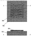
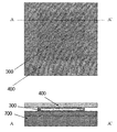
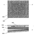
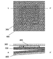
도 1 내지 14는 본 발명의 일 실시예에 따른 유연 전자소자의 제조방법의 단계도이다.
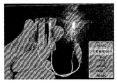
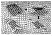
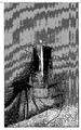
도 15은 본 발명에 따라 제조된 유연 배터리의 사진이고, 도 16은 제조공정을 설명하는 사진이다.
도 17은 본 발명의 일 실시예에 따라 희생기판에서 제조된 후 전사되는 배터리의 위치를 설명하는 도면이다.
도 18 내지 30은 본 발명의 일 실시예에 따른 유연 배터리의 제조방법을 설명하는 도면이다.
도 31 및 32는 각각 본 발명에 따라 제조된 배터리층(300)이 중성 역학층의 영향 내에 위치하지 못하는 경우와, 중성 역학층 영향 내에 위치하는 경우의 유연 배터리를 굽힌 사진이다.
도 33은 본 발명에 따라 제조된 유연 배터리에 대한 굽힘 테스트 모습이고, 도 34는 본 발명에 따른 유연 배터리의 충방전 테스트 결과이다.
도 35는 본 발명에 따른 유연 배터리의 쿨롱 효율(Coulombic efficiency) 결과이다.
도 36은 본 발명의 일 실시예에 따른 유연 배터리의 싸이클 테스트 결과이다.
도 37은 100싸이클의 충방전이 진행되는 경우, 기판 조건과 볼륨 변화와의 관계를 정리한 결과이다.
도 38 및 39는 본 발명에 따른 배터리로서 리튬이온배터리와 유기전계발광소자(OLED)를 중성역학층 위치에 구비시킨, 유연 발광소자의 구성도와 사진이다.
이하 바람직한 실시예 및 도면을 이용하여 본 발명을 상세히 설명한다. 하지만, 다음에 소개되는 실시예들은 당업자에게 본 발명의 사상이 충분히 전달될 수 있도록 하기 위한 예로서 제공되는 것이다. 따라서 본 발명은 이하 설명된 실시예들에 한정되지 않고 다른 형태로 구체화될 수도 있다. 그리고 도면들에 있어서, 구성요소의 폭, 길이, 두께 등은 편의를 위하여 과장되어 표현될 수도 있다. 명세서 전체에 걸쳐서 동일한 참조번호들은 동일한 구성요소들을 나타낸다.
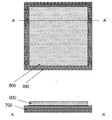
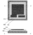
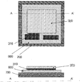
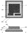
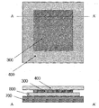
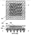
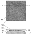
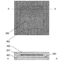
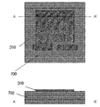
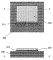
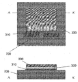
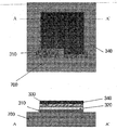
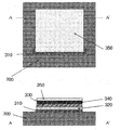
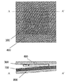
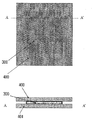
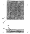
또한, 본 명세서에 첨부된 도면은 모두 전체 평면도 및 부분 단면(A-A')을 절개한 단면도의 형식으로 해석된다.
본 명세서에서 유연 기판은 유연성, 즉, 플렉서블 특성을 가지는 임의의 모든 기판을 다 포함하는 것으로 해석되며, 보다 명확하게는 플렉서블한 중합체 기판을 의미한다.
도 1 내지 14는 본 발명의 일 실시예에 따른 유연 전자소자의 제조방법의 단계도이다. 본 발명에서 상기 전자소자는 고온(예를 들어 섭씨 300도 이상) 등과 같은 극심한 조건에서 제조되는 전자소자로서, 본 발명의 일 실시예에서의 전자소자는 리튬 이온 배터리와 같은 이차전지이다. 하지만, 본 발명의 범위는 이에 제한되지 않으며, 폴링 공정 등과 같은 고온 공정이 일부 소자층에 적용되는 압전소자 등도 상기 전자소자에 해당될 수 있으며, 이 또한 본 발명의 범위에 속한다.
도 1을 참조하면, 금속 호일(metal foil, 700)이 개시된다. 본 발명의 일 실시예에서, 상기 금속 호일(700)은 구리 호일로서, 상기 구리 호일은 추후 설명되는 식각 공정에서 특정 화학액과 효과적으로 반응하여 식각된다.
도 2를 참조하면, 상기 금속 호일(700) 상 고정기판(800)이 적층된다. 본 발명에서 상기 고정기판(800)은 분리 후 얇은 두께의 이차전지를 잡아주는 역할을 수행하여, 분리 후 소자가 깨어지는 문제를 방지한다. 본 발명의 일 실시예서 상기 고정기판(800)으로 그래핀이 사용되었으나, 본 발명의 범위는 이에 제한되지 않는다.
도 3을 참조하면, 상기 그래핀 고정기판(800) 상에 집전체(310)가 박막 형태로 적층된다. 상기 집전체(310) 는 이차전지에서 발생하는 전류를 수집(collect)하여 외부로 전달하는 기능을 수행하며, 백금(Pt), 알루미늄(Al), 구리(Cu)등과 같은 금속 재료를 사용하나, 전극활물질 또는 리튬과 반응하여 리튬의 가역적 반응을 방해하지 않고 전류를 통할 수 있다면 특별히 한정되지 않는다. 또한 상기 집전체(310)와 고정기판(800) 사이에는 접착력 향상을 위하여 티타늄(Ti), 크롬(Cr)과 같은 부착층(미도시)이 사용될 수 있다.
도 4를 참조하면, 상기 집전체(310) 위로 전극물질이 증착되어, 양극(320)이 형성된다. 본 발명에서 사용된 리튬 이차전지의 경우, 양극으로 LiCoO2, LiNiO2등의 층상계 소재, LiMn2O4등의 스핀넬계 소재, LiFePO4등의 올리빈계 소재, Li2FeSiO4 등의 실리케이트계소재와 같은 리튬산화물을 사용할 수 있다.
도 5를 참조하면, 상기 양극(320) 적층 후, 리튬산화물과 같은 고온 열처리를 통하여 물질의 결정화가 진행된다. 예를 들어 고속열처리공정(rapid thermal process)의 경우는 보통 300℃ 이상, 바람직하게는 500℃ 이상에서 10분 이상, 가열로(furnace)의 경우는 500℃ 이상에서 2시간 이상의 열처리가 진행된다. 본 발명이 적용되는 이차전지에서, LiCoO2 물질의 결정화를 위한 고온 열처리 공정은 고성능의 고상 리튬 이온 전지에서 매우 중요한 공정인데, 이는 고상의 리튬 확산은 결정 결함에 의하여 방해 받으므로, 고순도의 결정성을 확보하는 것은 매우 중요하기 때문이다. 또한 상기 희생기판은 상기 고온의 열처리 공정을 견뎌야 하므로 500℃ 이상의 용융점을 갖는 것이 바람직하다.
도 6을 참조하면, 결정화가 진행된 양극(320) 상으로 전해질층(330)이 적층된다. 본 발명의 일 실시예에서 상기 전해질층(330)의 전해질은 고체 전해질이며, LiPON(Lithium Phosphorus Oxynitride)과 같은 물질을 주로 사용하였다. 하지만, 리튬이온의 이동에 의하여 전기를 통할 수 있다면 특별히 한정되지 않는다. 이와 같이 본 발명은 고온 공정에 취약한 전해질층(330) 형성 이전 열처리를 완료하여, 금속 호일 상에서 우수한 효율의 이차전지를 제조할 수 있다.
도 7을 참조하면, 상기 전해질층(330) 위로 음극(340)이 적층되는데, 상기 음극 물질로는 주로 리튬금속, 리튬합금, 탄소계 재료, 실리콘, 실리콘 합금 등이 사용될 수 있으나, 리튬의 삽입과 탈리가 가역적으로 가능한 물질이라면 특별히 한정되지 않는다.
특히 전해질/음극 등은 고순도의 결정성 확보를 위한 열처리 공정에서 열화되기 때문에, 양극만을 적층한 후, 열처리하고, 그 이후 양극 상에 전해질층과 음극을 적층하여 박막 이차전지를 제조하고, 하기 설명되는 식각 공정을 통하여 고정기판(800)상에서 제조된 이차전지를 상기 금속호일(700)로부터 분리시킨다.
도 8을 참조하면, 상기 음극(340) 위로 포장재층(350)이 적층된다. 본 발명의 일 실시예에서 상기 포장재층(350)은 전극 물질의 외부와의 접촉을 막아 전지의 성능을 저하시키는 부수적 반응을 방지하며, 당업계에서 사용되는 임의의 모든 물질이 상기 포장재층(350)에 포함될 수 있으며, 이상의 공정을 통하여 단위 이차전지 소자(300)가 금속호일(700) 상에 제조된다.
도 9는 본 발명의 일 실시예에 따라 대면적의 이차전지(300)가 금속호일(700) 상에서 제조된 예를 설명하는 도면이다.
도 10은 금속호일(700) 상에 어레이(array) 형태로 적층된 복수 개의 단위 이차전지 소자(300)를 설명하는 도면이다.
도 11을 참조하면, 상기 금속호일(700) 상의 이차전지 소자(300) 상부에 지지기판(400)이 접합된다. 본 발명에서 상기 지지기판(400)은 이차전지 소자(300)가 금속 호일(700)로부터 분리된 후, 이차전지 소자(300)를 원하는 기판으로 전사하는 매체로서 기능하며, 동시에 하부 고정기판(800)과 함께 분리시 깨질 수 있는 이차전지 소자(300)를 지지하는 고정시켜주는 역할을 수행한다. 상기 지지기판(400)으로, 예를 들어 접합력을 갖는 폴리디메틸실록산 (PDMS)이 사용될 수 있다.
도 12 참조하면, 상기 지지기판(400)으로 이차전지 소자(300)를 지지시킨 후, 상기 금속호일(700)을 제거하는 식각 공정을 진행한다.
본 발명의 일 실시예에 따른 상기 식각 공정은, 상부에 이차전지 소자가 제조된 하부 금속호일의 구성물질과 반응하여 이를 제거할 수 있는 식각액을 사용하는 습식 식각 공정이다. 예를 들어 본 발명의 일 실시예에서 상기 금속 호일은 구리 호일이므로, 상기 식각액은 FeCl3와 같은 구리 식각액이 사용된다.
도 13을 참조하면, 도 12에 따른 식각 공정에 따라 금속호일(700)은 제거되며, 이로써 고정기판(800)상의 이차전지는 금속호일(700)로부터 분리된다.
도 14는 본 발명의 또 다른 일 실시예에 따라 상기 분리된 이차전지 소자(300)의 측면과 상부를 밀봉하여 지지기판(400)의 물질층 내부로 이차전지 소자(300)를 삽입하는 구조를 설명하는 도면이다.
본 발명의 상술한 바와 같이 금속 호일 상에서 그래핀과 같은 고정기판을 사용하여 이차전지 등의 전자 소자를 제조하고, 금속 호일을 바로 식각하여 이차전지를 분리한다. 따라서, 상대적으로 실리콘과 같은 희생기판을 사용하여 소자를 제조한 후, 분리하는 종래 기술에 비하여 공정이 경제적이고, 아울러 얇은 두께의 금속 호일을 습식 식각 공정을 통하여 효과적으로 제거할 수 있다.
본 발명의 또 다른 일 실시예는 배터리의 용량이, 기판에 구비된 배터리의 기계적 스트레스에 의하여 가변되는 점을 발견하였다. 본 발명은 특히 운모와 같은 층상 기판에서 제조된 배터리의 경우, 유연 기판으로 전사되면, 배터리의 용량이 10% 이상 증가하는 독특한 기계적-전기적 관계에 주목하여, 본 발명에 이르게 되었다. 본 명세서에서 유연 기판은 유연성, 즉, 유연 특성을 가지는 임의의 모든 기판을 다 포함하는 것으로 해석되며, 보다 명확하게는 유연한 중합체 기판을 의미한다. 또한, 본 발명에서 배터리는 일차전지, 이차전지를 모두 포함하며, 이 외에도 전력을 생산할 수 있는 임의의 모든 소자가 배터리에 속하며, 본 발명의 범위는 하기 도면에서 설명하는 이차전지에 의하여 제한, 한정되지 않는다.
본 발명의 일 실시예에 따라 제조된 유연 배터리는, 상기 유연 배터리의 배터리층이 운모 기판에서 제조된 후, 유연 기판으로 전사된 것으로, 상기 유연 배터리는 상기 운모 기판 상의 배터리보다 높은 용량을 가지며, 이것은 상기 유연 배터리가 상기 운모 기판 상에서 제조된 직후의 배터리보다 낮은 기계적 스트레스를 가지며, 이러한 상기 낮은 기계적 스트레스로 인하여 상기 유연 배터리는 상기 운모 기판 상의 배터리보다 증가된 용량을 갖는다.
본 발명의 일 실시예에서 상기 배터리는 순차적으로 적층된 집전체, 양극, 전해질 및 음극을 포함하며, 이 중 상기 집전체, 양극은 운모기판에 제조된 후, 열처리된다. 이로써 전해질의 열처리에 따른 배터리 소자의 성능 열화의 문제를 해결한다. 즉, 본 발명은 배터리 소자 제조시 요구되는 공정의 최고점 이상의 용융점 또는 유리전이온도를 갖는 기판(이하 희생기판)에 배터리(배터리, LED 소자)를 제조한 후, 이를 원하는 소자기판에 전사시킨다. 특히 배터리, LED 소자와 같은 배터리의 기능층 중 고온 공정을 통하여 성능이 개선되는 소자층만을 우선 희생기판에 적층하고, 열처리한다. 이로써 전사 후에도 원하는 소자 성능을 그대로 유지할 수 있다.
더 나아가, 이와 같이 제조된 배터리를 유연 기판에 전사하여 용량을 증대시킨 후, 또 다른 유연 물질을 배터리에 도포하여, 유연 물질층 내에 배터리가 구비된 배터리 소자를 제조한다. 이때, 상기 배터리는 유연물질층 내의 중성역학층에 위치하도록 구성한다. 본 발명에서 중성역학층(Mechanical Neural Plane)은 아래에서 인가되는 압축응력과 위쪽에서 인가되는 인장응력으로부터 이론 변형율 0이 되는 층으로서, 특히 휘어지는 경우, 중성역학층이 받는 기계적인 스트레스는 이론상 0이 되는 영역이다. 본 발명은 이러한 중성역학층에 희생기판 상에 제조된 배터리층을 구비시켜, 추후 유연기판이 휘어지는 경우에도 안정된 기계적 견고성을 갖게 한다.
또한 본 발명은 높은 기계적 스트레스를 가하는 기판으로 층상 기판을 사용하는데, 특히 이러한 층상 기판은 각 층들은 박리 방식으로 제거되며, 이로써 배터리에 인가되는 기계적 스트레스(응력)의 급격한 변화를 방지할 수 있다. 또한, 물리적인 방식(즉, 박리 방식)으로 하부 기판을 제거시킨 본 발명은 식각액 등을 사용하여 화학적으로 하부기판을 제거하는 종래 기술에 비하여, 월등히 경제적이고, 안정적인 장점이 있다.
도 15는 본 발명에 따라 제조된 유연 배터리의 사진이고, 도 16은 제조공정을 설명하는 사진이다.
도 15를 참조하면, 상하부층의 폴리디메틸실록산(PDMS)과 상기 PDMS층 내부에 리튬이온배터리의 소자층이 구비되는 것을 알 수 있다.
도 16을 참조하면, 먼저 운모(Mica) 상에서 리튬이온배터리(LIB)를 제조하고, 상기 운모의 층을 기계적인 방식(테이프 이용)으로 박리시켜, 유연성을 확보한다. 이후 이를 PDMS 기판에 적층하고, 상부 PDMS를 적층하여, 도 1의 내부 삽입 이미지와 같은 유연 배터리를 제조한다.
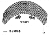
도 17은 본 발명의 일 실시예에 따라 희생기판에서 제조된 후 전사되는 배터리의 위치를 설명하는 도면이다.
도 17을 참조하면, 본 발명에 따른 소자는 적색 점선으로 표시되는 중성역학층에 구비되며, 이에 따라 벤딩시 발생하는 인장응력(tensile strength)과 압축응력(compressive strength)의 합은 0이 되며, 그 결과 벤딩 시에도 배터리와 같은 배터리는 견고한 기계적 특성을 갖게 된다. 즉, 본 발명에 따른 배터리는 벤딩시 발생하는 압축응력과 인장응력으로부터 이론 변형율 0의 중성 역학층(10)을 생성하게 된다.
본 발명의 일 실시예에서는 유연 소재 사이에 딱딱한 소재 특성의 무기물질로 이루어지는 배터리층을 구비시키며, 이때 상기 배터리층은 폴리머 소재 내에서 중성 역학층에 위치하거나 영향 범위내에 위치할 수 있다. 따라서, 본 발명에서는 전체 소자의 중성 역학층의 영향 범위내에 배터리층을 위치시킴으로 해서, 실제 휨에 따라 부서지기 쉬운 배터리층의 유연 특성을 향상시켰다. 특히 상기 배터리층은 중성 역학층으로부터 전체 두께의 ±20%에 해당하는 범위 내에 위치할 때 가장 안정적인 특성을 가지게 된다.
도 18 내지 30은 본 발명의 일 실시예에 따른 유연 배터리의 제조방법을 설명하는 도면이다. 여기에서 상기 배터리는 리튬이온배터리이나, 본 발명의 범위는 이에 제한되지 않는다.
도 18 내지 24를 참조하면, 상기 운모기판(700) 상에 집전체(310), 양극(320), 전해질(330)과 음극(340)이 순차적으로 적층된다.
여기에서 집전체(310)는 박막 형태로 적층되며, 상기 집전체(310) 는 배터리에서 발생하는 전류를 수집(collect)하여 외부로 전달하는 기능을 수행하며, 백금(Pt), 알루미늄(Al), 구리(Cu)등과 같은 금속 재료를 사용하나, 전극활물질 또는 리튬과반응하여 리튬의 가역적 반응을 방해하지 않고 전류를 통할 수 있다면 특별히 한정되지 않는다. 또한 상기 집전체(310)와 수소 함유 비정질 실리콘(800) 사이에는 접착력 향상을 위하여 티타늄(Ti), 크롬(Cr)과 같은 부착층(미도시)이 사용될 수 있다. 상기 전류집전체(310) 위로 전극물질이 증착되어, 양극(320)이 적층된다. 본 발명에서 사용된 리튬 배터리의 경우, 양극으로 LiCoO2, LiNiO2등의 층상계 소재, LiMn2O4등의 스핀넬계 소재, LiFePO4등의 올리빈계 소재, Li2FeSiO4 등의 실리케이트계소재와 같은 리튬산화물을 사용할 수 있다. 이후 상기 양극(320) 적층 후, 리튬산화물과 같은 고온 열처리를 통하여 물질의 결정화가 진행된다. 예를 들어 고속열처리공정(rapid thermal process)의 경우는 보통 300℃ 이상, 바람직하게는 500℃ 이상에서 10분 이상, 가열로(furnace)의 경우는 500℃ 이상에서 2시간 이상의 열처리가 진행된다. 본 발명이 적용되는 배터리에서, LiCoO2 물질의 결정화를 위한 고온 열처리 공정은 고성능의 고상 리튬 이온 전지에서 매우 중요한 공정인데, 이는 고상의 리튬 확산은 결정 결함에 의하여 방해 받으므로, 고순도의 결정성을 확보하는 것은 매우 중요하다. 또한 상기 희생기판은 상기 고온의 열처리 공정을 견뎌야 하므로 500℃ 이상의 용융점을 갖는 것이 바람직하다. 이후 상기 열처리 후 적층된 음극(340)위에 포장재(350)가 적층되며, 이로써 집전체-양극-전해질-음극-포장재로 이루어진 배터리층(300)이 운모기판(700) 상에 제조된다. 상기 배터리층(300)에 인가되는 기계적 스트레스는 상당히 높은 편인데, 이것은 운모기판이 가지는 딱딱한 특성에 기인한다.
도 25 및 26을 참조하면, 상기 배터리층(300) 상에 지지층(400)이 접착되고, 이후 하부 운모기판(700)의 층상이 기계적 방식(예를 들면, 접착용 테이프(800)의 접착 후 떼어내는 방식)으로 제거된다. 본 발명의 일 실시예에서 상기 지지층(400)은 폴리디메틸실록산과 같은 폴리머 물질이 사용되었으나, 본 발명의 범위는 이에 제한되지 않는다. 본 발명에서는 이와 같은 기계적 방식의 박리를 복수 회 진행하며, 특히 박리 횟수를 조절하여 층상 기판의 두께를 조절할 수 있다. 이때 하부 층상기판은 모두 제거되거나, 일부 유연성을 갖는 수준으로 잔존할 수 있다. 이 경우 하부에 잔존하는 층상기판은 일종의 하부 지지기판으로 작용할 수 있다.
도 26 내지 28를 참조하면, 동일한 방식으로 하부 운모 기판을 기계적인 방식으로 박리시킴으로써, 지지층(400)에 접착된 프리스탠딩 형태의 배터리층(300)이 완성된다. 본 발명은 특히 이러한 층상 기판을 폴리디메특실록산과 같은 유연 기판으로 변경하는 경우, 상기 배터리에 가해지는 기계적 스트레스가 완화되며, 이로써 배터리의 용량을 증대시켰다.
이후 본 발명에서는 2 가지 방식의 플레서블 소자를 제공하는데, 어떠한 경우에도 도 14의 지지층(400)에 접착된 배터리층(400) 위치는 양측의 폴리머층 으로부터 생성된 중성 역학층 영향 범위내에 위치하게 된다.
도 29에서는 도 28의 지지층(이하 제 1 지지층(400))에 접착된 배터리층(300)의 반대 쪽에 또 다른 지지층(이하 제 2 지지층(401))이 접착된다. 이로써 운모기판에서 제조된 후 전사된 배터리층은 두 개의 폴리머 물질층 사이에 끼워진 형태가 되며, 내부 소자에 인가되는 기계적 스트레스는 운모기판에 비하여 적다.
도 30에서는 또 다른 방식으로 지지층(400)에 접착된 배터리층(300)위로 상기 지지층과 동일한 물질의 폴리머를 도포하여, 덮는 방식으로 개시한다. 이 경우, 배터리층(300)은 지지층(400) 사이로 삽입되어, 외부로 노출되지 않으나, 도 3과 동일하게 상기 배터리층(300)은 양 지지층(400) 사이의 중성역학층의 영향 범위 내로 전사되며, 이로써 굽힘과 같은 외부 작용에도 안정된 물리적 상태를 이룬다. 상기 배터리층(300)은 중성 역학층으로부터 전체 두께의 ±20%에 해당하는 범위 내에 위치할 때 가장 안정적인 특성을 가지게 된다.
도 31 및 32는 각각 본 발명에 따라 제조된 배터리층(300)이 중성 역학층의 영향 내에 위치하지 못하는 경우와, 중성 역학층 영향 내에 위치하는 경우의 유연 배터리를 굽힌 사진이다.
도 31 및 32를 참조하면, 배터리층(300)이 중성 역학층의 영향내에 위치하지 못하는 경우, 수 차례의 굽힘 테스트 후에 배터리층(300)이 깨지게 되나(도 17 참조), 배터리층(300)이 중성 역학층(300)의 영향내에 위치하는 경우, 배터리층(300)이 안정된 형태를 이룬다.
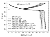
도 33은 본 발명에 따라 제조된 유연 배터리에 대한 굽힘 테스트 모습이고, 도 34는 본 발명에 따른 유연 배터리의 충방전 테스트 결과이다.
도 33 및 34를 참조하면, 희생기판인 운모기판을 제거함에 따라 스트레스 완화(stress relaxation)의 영향으로 10%의 용량 증가를 보였다. 즉, 본 발명은 운모 기판상에서 제조된 리튬이차전지 배터리의 용량 증대를, 하부의 층상 기판의 기계적, 단계적 박리, 제거로써 달성하였다. 이는 유연 기판 사용이, 벤딩 등의 기계적 효과를 발생시킬 뿐만 배터리의 용량 증대 효과를 발생시키는 점을 증명한다. 특히 적색으로 표시되는 유연 기판으로 기판 변경된 배터리는 1차 싸이클인 경우나, 100차 싸이클인 경우나 모두 증대된 용량을 갖는 것을 알 수 있다.
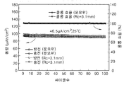
도 35는 본 발명에 따른 유연 배터리의 쿨롱 효율(Coulombic efficiency) 결과이다.
도 35를 참조하면, 본 발명에 따른 유연 배터리는 완화된 기계적 스트레스에 의하여 일정한 쿨롱 효율을 나타냄을 알 수 있다.
도 36은 본 발명의 일 실시예에 따른 유연 배터리의 싸이클 테스트 결과이다.
도 36을 참조하면, 본 발명에 따라 제조된 유연 배터리는 증대된 용량뿐만 아니라, 일정한 용량 유지 특성을 보임을 알 수 있다.
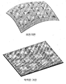
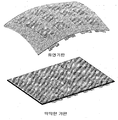
도 37은 100싸이클의 충방전이 진행되는 경우, 기판 조건과 볼륨 변화와의 관계를 정리한 결과이다.
도 37을 참조하면, 볼륨 변화로부터 발생하는 내부 스트레스는 적색 화살표로 표시되며, 운모 및 PDMS 상에서의 스트레스 분포 또한 도 23에서 표시된다.
상기 결과는 폴리머 기판으로 전사된 배터리는 가해지는 휨 강도에 비하여 매우 낮은 유도 스트레스를 갖는 것을 나타낸다. 이로써 리튬이온배터리 용량 또한 기판 변경으로 인한 스트레스 감소 효과로 인하여 증가되는 것을 알 ㅅ 있다.
도 38 및 39는 본 발명에 따른 배터리로서 리튬이온배터리와 유기전계발광소자(OLED)를 중성역학층 위치에 구비시킨, 유연 발광소자의 구성도와 사진이다.
도 39를 참조하면, 리튬이온배터리(LIB) 상에 OLE와 같은 발광소자층을 구비시키고, 상기 OLED 상에 PDMS 층을 도포시켜, 유연물질층 내에 배터리층이 구비된 것을 알 수 있다. 이 때, 상기 리튬이온배터리(LIB) 및 유기전계발광소자(OLED)는 유연 물질층 내에서 중성역학층 위치에 구비되는 것이 바람직하며, 이로써 벤딩시 무기층이 깨어지는 문제를 감소시킬 수 있다.
이하 도면을 이용하여 본 발명의 일 실시예에 에 따른 다층 이차전지 제조방법을 상세히 설명한다.
도 40 내지 54는 본 발명의 일 실시예에 따른 다층 이차전지의 단위 이차전지 제조방법을 설명하는 도면이다.
도 40을 참조하면, 기판(700)이 개시되며, 상기 기판(700)으로는 유리 또는 사파이어 기판이 사용될 수 있다. 본 발명에서 상기 기판(700) 상에서는 이차전지가 제조된 후, 분리되는 기판이므로, 이하 희생기판이라 지칭한다.
도 41을 참조하면, 상기 희생기판(700) 상에는 수소가 도핑된 비정질 실리콘층(800)이 적층되는데, 상기 비정질 실리콘층(800) 적층은 통상의 반도체 공정(예를 들어 화학기상증착-스퍼터링 공정)에 따라 진행될 수 있으므로, 이에 대한 상세한 설명은 이하 생략한다.
도 42를 참조하면, 상기 비정질 실리콘층(800) 상에 집전체(310)가 박막 형태로 적층된다. 상기 집전체(310) 는 이차전지에서 발생하는 전류를 수집(collect)하여 외부로 전달하는 기능을 수행하며, 백금(Pt), 알루미늄(Al), 구리(Cu)등과 같은 금속 재료를 사용하나, 전극활물질 또는 리튬과반응하여 리튬의 가역적 반응을 방해하지 않고 전류를 통할 수 있다면 특별히 한정되지 않는다. 또한 상기 집전체(310)와 수소 함유 비정질 실리콘(800) 사이에는 접착력 향상을 위하여 티타늄(Ti), 크롬(Cr)과 같은 부착층(미도시)이 사용될 수 있다.
도 43을 참조하면, 상기 전류집전체(310) 위로 전극물질이 증착되어, 양극(320)이 적층된다. 본 발명에서 사용된 리튬 이차전지의 경우, 양극으로 LiCoO2, LiNiO2등의 층상계 소재, LiMn2O4등의 스핀넬계 소재, LiFePO4등의 올리빈계 소재, Li2FeSiO4 등의 실리케이트계소재와 같은 리튬산화물을 사용할 수 있다.
도 44를 참조하면, 상기 양극(320) 적층 후, 리튬산화물과 같은 고온 열처리를 통하여 물질의 결정화가 진행된다. 예를 들어 고속열처리공정(rapid thermal process)의 경우는 보통 300℃ 이상, 바람직하게는 500℃ 이상에서 10분 이상, 가열로(furnace)의 경우는 500℃ 이상에서 2시간 이상의 열처리가 진행된다. 본 발명이 적용되는 이차전지에서, LiCoO2 물질의 결정화를 위한 고온 열처리 공정은 고성능의 고상 리튬 이온 전지에서 매우 중요한 공정인데, 이는 고상의 리튬 확산은 결정 결함에 의하여 방해 받으므로, 고순도의 결정성을 확보하는 것은 매우 중요하다. 또한 상기 희생기판은 상기 고온의 열처리 공정을 견뎌야 하므로 500℃ 이상의 용융점을 갖는 것이 바람직하다.
도 45를 참조하면, 결정화가 진행된 양극(330) 상으로 전해질층(330)이 적층된다. 본 발명의 일 실시예에서 상기 전해질층(330)의 전해질은 고체 전해질이며, LiPON(Lithium Phosphorus Oxynitride)과 같은 물질을 주로 사용하였다. 하지만, 리튬이온의 이동에 의하여 전기를 통할 수 있다면 특별히 한정되지 않는다.
도 46을 참조하면, 상기 전해질층(330) 위로 음극(340)이 적층되는데, 상기 음극 물질로는 주로 리튬금속, 리튬합금, 탄소계 재료, 실리콘, 실리콘 합금 등이 사용될 수 있으나, 리튬의 삽입과 탈리가 가역적으로 가능한 물질이라면 특별히 한정되지 않는다.
특히 전해질/음극 등은 고순도의 결정성 확보를 위한 열처리 공정에서 열화되기 때문에, 양극만을 적층한 후, 열처리하고, 그 이후 양극 상에 전해질층과 음극을 적층하여 박막 태양전지를 제조하고, 이로부터 제조된 단위 박막 태양전지를 순차적으로 적층하여 3차원 구조의 리튬 이온 배터리를 제조한다.
도 47을 참조하면, 상기 음극(340) 위로 포장재층(350)이 적층된다. 본 발명의 일 실시예에서 상기 포장재층(350)은 전극 물질의 외부와의 접촉을 막아 전지의 성능을 저하시키는 부수적 반응을 방지하며, 당업계에서 사용되는 임의의 모든 물질이 상기 포장재층(350)에 포함될 수 있다.
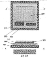
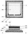
이상의 공정을 통하여 단위 이차전지 소자(300)가 희생기판(700) 상에 제조된다. 도 48을 참조하면, 상술한 방식에 따라 제조된 양극-전해질-음극으로 구성된 하나의 대면적 이차전지 소자(300)가 개시되며, 도 10에서는 비정질 실리콘층(800) 상에 어레이 형태로 적층된 복수 개의 단위 이차전지 소자(300)가 개시된다.
도 49를 참조하면, 상기 이차전지 소자(300) 상에 지지기판(400)이 접합된다. 본 발명에서 상기 지지기판은 이차전지 소자(300)가 하부 기판으로부터 분리된 후, 이차전지 소자(300)를 고정시켜주는 역할을 수행하며, 예를 들어 접합력을 갖는 폴리디메틸실록산(PDMS)이 상기 지지기판(400)으로 사용될 수 있다.
도 50을 참조하면, 도 48 또는 도 49의 이차전지 소자(300), 특히 비정질 실리콘층(800)상에서 제조된 이차전지 소자(300)가 개시된다.
도 51을 참조하면, 도 50의 희생기판(700) 후면으로 레이저 빔이 조사되며, 이때 비정질 실리콘 층(800) 내에 존재하는 수소가 가스화되어 배출되며(outgasing), 이로써 비정질 실리콘 층(800)이 박리제거된다. 따라서, 상기 희생기판(700)은 레이저가 투과될 수 있는 수준의 투명도를 갖는 것이 바람직하며, 예를 들어 유리 또는 사파이어가 상기 희생기판으로 사용될 수 있다.
도 52를 참조하면, 도 51의 공정을 통하여 분리된 이차전지의 타측에도 동일한 지지층(400)이 접합되고, 도 53을 참조하면, 상기 이차전지의 상하면 뿐만 아니라 측면에도 지지층(400)이 구비된다.
도 54는 상술한 공정에 따라 제조된 박막 이차전지(300)가 다층으로 적층된 다층 이차전지의 구조를 설명하는 도면이다.
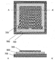
도 54를 참조하면, 기판(1000) 상에 이차전지(300)가 다층으로 적층되며, 이때 상기 이차전지(300)는 희생기판에서 제조된 후, 열처리까지 완료된 것으로, 레이저 빔 조사 등을 통하여 희생기판(700)으로부터 분리된다. 또한 본 발명의 일 실시예에서 다층 구조의 이차전지(300) 사이에는 에폭시 등과 같은 접착제(900)가 구비된다. 즉, 본 발명은 희생기판에서 제조된 후, 열처리까지 완료된 이차전지를 기판(1000)으로 순차적으로 복수 회 전사시킴으로써 도 15 등과 같은 다층 구조의 이차전지를 제조한다.
특히 본 발명은 이러한 다층의 두께를 전사 횟수 제어를 통하여 조절할 수 있으며, 이로부터 이차전지의 유연성 정도를 용이하게 결정할 수 있다. 예를 들어, 다층 이차전지의 두께가 10um이면 유연하나, 단위두께가 100um까지 두꺼워 지면 깨지기 쉬우나, 이처럼 접착제를 통하여 무기 박막재료를 seperate하여 적층하면 유연성이 증가한다.
더 나아가, 본 발명의 일 실시예에서 상기 이차전지(300)는 도 12, 13과 같이 외부로 이차전지 소자가 노출된 형태이거나, 도 53와 같이 지지층(400)에 의하여 밀봉된 형태일 수 있으며, 적어도 도 54와 같이 접착제(900)에 의하여 상기 이차전지가 다층을 이루는 이상, 이는 본 발명의 범위에 속한다.
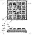
도 55는 본 발명의 일 실시예에 따라 대면적의 다층 이차전지가 단일 구성으로 제조된 예를 설명하는 도면이다. 더 나아가, 본 발명의 일 실시예에서는 도 10과 같은 어레이 형태로 이차전지를 제조하는 경우, 각각의 단위 이차전지(300)를 기판(1000)상에 순차적으로 적층시킬 수 있다. 이로써 도 55에서와 같이 유연기판(플렉서블 기판)이나 딱딱한 기판상에서도 도 54와 같은 적층 형태의 이차전지가 제조될 수 있다. 특히 딱딱한 기판인 경우, 상기 다층 이차전지와 기판(1000) 사이에는 별도의 이차전지 등과 같은 별도 소자가 더 구비될 수 있다.
도 56은 도 49에 기반한 어레이 형태로 다층 이차전지가, 유연기판 또는 딱딱한 기판에서 제조된 형태를 설명하는 도면이다.
더 55 및 56에 따른 다층 이차전지는 제한된 면적에서도 다수의 박막형 이차전지가 구비될 수 있으므로, 면적당 전력 생산 효율이 우수하다.
도 57에서는 유연한 LED디스플레이와 같은 전자 소자에 결합된 유연 다층 이차전지 적용예를 설명하는 도면이다.
본 발명에 따른 다층 이차전지는 우수한 용량 효율을 가질 수 있는데, 예를 들어 다층 이차전지(두께 10um, 넓이 1.5 x 1.5 cm) 용량이 대략 1mAh 정도이고, 이를 12x 18 cm (노트 사이즈)에 10층(두께 100um)을 적층하면, 구동 볼트 4 V의 충전 용량1440mAh 정도도 가능할 수 있다. 이와 같이 본 발명에 따른 다층 이차전지는 2차원적인 면적뿐만 아니라 다층의 높이를 통하여 용량, 유연성 등을 효과적으로 제어할 수 있다.
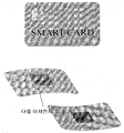
도 58은 박막 형태가 요구되는 스마트 카드에 본 발명에 따른 다층 이차전지(회색부분)가 구비된 경우를 설명하는 도면이다.
또한 본 발명에 따른 이차전지는 기판이 양쪽으로 다층으로 적층될 수 있는데, 예를 들어 도 59 및 60은 단일 또는 어레이 형태의 다층 이차전지가 기판 양면에 형성된 경우를 설명하는 도면이다.
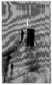
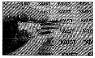
도 61은 본 발명의 일 실시예에 따라 제조된 다층 이차전지의 실제 이미지이다.
도 61에 도시된 이미지는, 유리기판위 비정질 실리콘 위에 무기물 전극재료와 금속전극을 증착한 후 레이저 리프트 오프를 통해 얻은 배터리 전극의 이미지로서, 본 실험예에서는 PECVD를 통하여 50 nm 비정질 실리콘 증착하고, 다시 스퍼터(Sputter)를 이용하여 무기물 전극재료(100 nm-5 um), 금속 전극(100 nm)을 증착하고, 500 mJ/cm2의 레이저를 이용하여 박리시켰다.
상술한 바와 본 발명에 따른 다층 이차전지는, 박막 이차전지가 이층 이상으로 적층된 형태를 이루며, 상기 박막 이차전지는 희생기판에서 열처리시 열화되는 소자층을 제외한 소자층, 특히 열처리에 의하여 특성이 향상되는 소자층의 열처리를 완료한 후, 나머지 공정을 진행하고, 다시 완성된 이차전지 소자를 원하는 기판에 전사된 형태이다. 따라서, 전지 효율은 떨어뜨리지 않으면서도 면적당 높은 전력생산율을 가질 수 있다. 아울러 다층 구조의 수를 제어함으로써 최종 사용되는 제품 기판의 유연성에 대응되는 유연성을 갖는 다층 이차전지를 제조할 수 있으며, 더 나아가 다층 이차전지의 유연성을 다층 수를 제어함으로써 효과적으로 조절할 수 있다. 이상 본 발명의 바람직한 실시예를 참조하여 설명하였지만 해당 기술 분야의 숙련된 당업자라면 하기의 특허청구범위에 기재된 본 발명의 사상 및 영역으로부터 벗어나지 않는 범위 내에서 본 발명을 다양하게 수정 및 변경시킬 수 있음을 이해할 수 있을 것이다.
본 발명에 따른 유연 전자소자 및 배터리는 전자제품에 사용되는 배터리 등에 적용될 수 있으므로, 그 결과 다양한 전자 산업 분야에 이용가능성이 인정된다.
Claims (22)
- 금속호일 상에 전자소자를 적층하는 단계; 및상기 금속호일을 식각하여 제거하는 단계를 포함하는 것을 특징으로 하는 유연 전자소자 제조방법.
- 제 1항에 있어서,상기 전자소자는 제조시 섭씨 300도 이상의 고온공정이 사용되며, 상기 금속호일 상에 고정기판을 적층하는 것을 특징으로 하는 유연 전자소자 제조방법.
- 제 2항에 있어서,상기 고정기판은 그래핀층인 것을 특징으로 하는 유연 전자소자 제조방법.
- 제 1항에 있어서, 상기 유연 전자소자 제조방법은,상기 적층된 고정기판 상에 전자소자를 제조하는 단계 후, 상기 전자소자 상에 전사기판을 접합시키는 단계를 더 포함하는 것을 특징으로 하는 유연 전자소자 제조방법.
- 금속호일 상에 집전체 및 양극을 순차적으로 적층하는 단계; 및상기 순차적으로 적층된 양극을 열처리하는 단계;상기 열처리된 양극 상에 전해질층 및 음극을 순차적으로 적층하여 이차소자를 제조하는 단계;상기 금속호일을 식각하여 제거하는 단계;를 포함하는 것을 특징으로 하는 유연 이차전지 제조방법.
- 제 5항에 있어서,상기 양극은 고온공정이 필요하며, 상기 금속호일 상에 고정기판을 적층하는 것을 특징으로 하는 유연 이차전지 제조방법.
- 제 6항에 있어서,상기 고정기판은 그래핀층인 것을 특징으로 하는 유연 전자소자 제조방법.
- 제 7항에 있어서, 상기 유연 전자소자 제조방법은,상기 적층된 고정기판 상에 이차소자를 제조하는 단계 후, 상기 이차소자 상에 전사기판을 접합시키는 단계를 더 포함하며, 상기 금속호일은 구리포일이며, 상기 습식 식각 공정의 식각액은 FeCl3인 것을 특징으로 하는 유연 이차전지 제조방법.
- 유연 배터리로서,상기 유연 배터리의 배터리층은 운모 기판에서 제조된 후, 유연 기판으로 전사된 것으로, 상기 유연 배터리는 상기 운모 기판상의 배터리보다 높은 용량을 갖는 것을 특징으로 하는 유연 배터리.
- 제 9항에 있어서,상기 유연 배터리는 상기 운모 기판 상에서 제조된 배터리보다 낮은 기계적 스트레스를 가지며, 상기 낮은 기계적 스트레스로 인하여 상기 유연 배터리는 상기 운모 기판 상의 배터리보다 증가된 용량을 갖는 것을 특징으로 하는 유연 배터리.
- 제 10항에 있어서,상기 유연 배터리의 배터리층은 상기 유연 기판을 하부에 포함하는 유연 물질층 내에 구비되며, 상기 배터리층은 상기 유연 물질층으로부터 생성된 이론 변형율 0의 중성역학 위치로부터 전체 두께의 ±20%에 해당하는 범위 내에 위치되는 것을 특징으로 하는 유연 배터리.
- 제 9항에 있어서, 상기 배터리층은,순차적으로 적층된 집전체, 양극, 전해질 및 음극을 포함하는 것을 특징으로 하는 유연 배터리.
- 제 12항에 있어서,상기 집전체, 양극은 운모기판에 제조된 후, 열처리된 것을 특징으로 하는 유연 배터리.
- 제 9항 내지 제 13항 중 어느 한 항에 따른 유연 배터리; 및상기 유연 배터리 상에 구비된 발광소자층을 포함하는 것을 특징으로 하는 유연 발광소자.
- 배터리 용량 증대 방법으로, 상기 방법은,상기 배터리의 하부 기판에 대한 스트레스를 완화시켜, 상기 배터리의 용량을 증가시키는 단계를 포함하는 것을 특징으로 하는 배터리 용량 증대 방법.
- 제 15항에 있어서, 상기 배터리의 용량을 증가시키는 단계는,층상 기판상에서 제조된 배터리의 상기 층상 기판을 유연 기판으로 변경하는 방식으로 진행되는 것을 특징으로 하는 배터리 용량 증대 방법.
- 배터리 용량 증대 방법으로, 상기 방법은,층상 기판 상에 배터리층을 제조하는 단계;상기 층상 기판를 박리시켜 제거하는 단계; 및상기 층상 기판이 제거된 배터리층을 상기 유연 기판에 전사하여, 상기 배터리층에 가해지는 기계적 스트레스를 완화시키는 단계를 포함하며, 상기 유연 기판 상의 배터리층에 인가되는 기계적 스트레스는, 상기 층상 기판상의 상기 배터리층에 인가되는 기계적 스트레스보다 약하며, 이로써 상기 배터리층의 용량은 증대되는 것을 특징으로 하는 배터리 용량 증대 방법.
- 제 17항에 있어서,상기 배터리층은 순차적으로 적층된 집전체, 양극, 전해질 및 음극이며, 여기에서 상기 층상 기판은 운모 기판인 것을 특징으로 하는 배터리 용량 증대 방법.
- 제 18항에 있어서, 상기 방법은,상기 집전체, 양극은 상기 층상 기판 상에서 열처리되는 단계를 더 포함하는 것을 특징으로 하는 배터리 용량 증대 방법.
- 기판(1000);상기 기판(1000) 상에 적어도 둘 이상 적층되며, 순차적으로 적층된 양극-전해질층-음극을 포함하는 이차전지(300); 및상기 이차전지(300) 사이에 구비되며, 상기 이차전지(300)를 접합시키는 접착재(900)를 포함하며, 여기에서 상기 양극-전해질층-음극 중 양극만 열처리되어 결정화된 것을 특징으로 하는 다층 이차전지.
- 제 20항에 있어서,상기 이차전지(300)는 별도의 희생기판에서 제조된 후 상기 기판(1000)으로 전사되며, 상기 희생기판 상에서 상기 양극이 열처리된 것을 특징으로 하는 다층 이차전지.
- 다층 이차전지 제조방법으로,희생기판(700) 상에 집전체(310) 및 양극(320)을 순차적으로 적층하는 단계;상기 양극(320)을 열처리하는 단계;상기 열처리된 양극(320) 상에 전해질(330), 음극(340)을 순차적으로 적층하여 이차전지(300)를 제조하는 단계;상기 이차전지(300)를 상기 희생기판(700)으로부터 분리한 후, 상기 분리된 이차전지(300)를 기판(1000) 상에 순차적으로 복수 회 전사시키는 단계를 포함하는 것을 특징으로 하는 다층 이차전지 제조방법.
Applications Claiming Priority (6)
| Application Number | Priority Date | Filing Date | Title |
|---|---|---|---|
| KR10-2012-0093852 | 2012-08-27 | ||
| KR1020120093852A KR20140027796A (ko) | 2012-08-27 | 2012-08-27 | 다층 구조의 이차전지 및 그 제조방법 |
| KR20120093853 | 2012-08-27 | ||
| KR10-2012-0093853 | 2012-08-27 | ||
| KR1020120107405A KR101340047B1 (ko) | 2012-09-26 | 2012-09-26 | 응력 완화에 의한 배터리 용량 증대 방법 및 이에 의하여 증대된 용량을 갖는 유연 배터리 |
| KR10-2012-0107405 | 2012-09-26 |
Publications (1)
| Publication Number | Publication Date |
|---|---|
| WO2014035014A1 true WO2014035014A1 (ko) | 2014-03-06 |
Family
ID=50183800
Family Applications (1)
| Application Number | Title | Priority Date | Filing Date |
|---|---|---|---|
| PCT/KR2012/011198 Ceased WO2014035014A1 (ko) | 2012-08-27 | 2012-12-20 | 유연 전자소자 및 그 제조방법, 응력 완화에 의한 배터리 용량 증대 방법 및 이에 의하여 증대된 용량을 갖는 유연 배터리 |
Country Status (1)
| Country | Link |
|---|---|
| WO (1) | WO2014035014A1 (ko) |
Cited By (2)
| Publication number | Priority date | Publication date | Assignee | Title |
|---|---|---|---|---|
| US10097228B2 (en) | 2015-04-23 | 2018-10-09 | Alliance Sports Group, L.P. | Method and apparatus for chip-on board flexible light emitting diode |
| US11906133B2 (en) | 2022-03-31 | 2024-02-20 | Alliance Sports Group, L.P. | Outdoor lighting apparatus |
Citations (5)
| Publication number | Priority date | Publication date | Assignee | Title |
|---|---|---|---|---|
| US20100021816A1 (en) * | 2004-02-26 | 2010-01-28 | Hei, Inc. | Flexible Circuit Having an Integrally Formed Battery |
| WO2010035197A1 (en) * | 2008-09-26 | 2010-04-01 | Koninklijke Philips Electronics, N.V. | Flexible all solid state battery with enhanced deposition freedom |
| WO2010086416A1 (en) * | 2009-01-30 | 2010-08-05 | Imec | Stretchable electronic device |
| KR20110050580A (ko) * | 2008-08-04 | 2011-05-16 | 파나소닉 주식회사 | 플렉시블 반도체 장치 및 그 제조 방법 |
| KR20120050021A (ko) * | 2010-11-10 | 2012-05-18 | 한국과학기술원 | 플라스틱 전지소자 제조방법, 이에 따라 제조된 플라스틱 전지소자 |
-
2012
- 2012-12-20 WO PCT/KR2012/011198 patent/WO2014035014A1/ko not_active Ceased
Patent Citations (5)
| Publication number | Priority date | Publication date | Assignee | Title |
|---|---|---|---|---|
| US20100021816A1 (en) * | 2004-02-26 | 2010-01-28 | Hei, Inc. | Flexible Circuit Having an Integrally Formed Battery |
| KR20110050580A (ko) * | 2008-08-04 | 2011-05-16 | 파나소닉 주식회사 | 플렉시블 반도체 장치 및 그 제조 방법 |
| WO2010035197A1 (en) * | 2008-09-26 | 2010-04-01 | Koninklijke Philips Electronics, N.V. | Flexible all solid state battery with enhanced deposition freedom |
| WO2010086416A1 (en) * | 2009-01-30 | 2010-08-05 | Imec | Stretchable electronic device |
| KR20120050021A (ko) * | 2010-11-10 | 2012-05-18 | 한국과학기술원 | 플라스틱 전지소자 제조방법, 이에 따라 제조된 플라스틱 전지소자 |
Cited By (3)
| Publication number | Priority date | Publication date | Assignee | Title |
|---|---|---|---|---|
| US10097228B2 (en) | 2015-04-23 | 2018-10-09 | Alliance Sports Group, L.P. | Method and apparatus for chip-on board flexible light emitting diode |
| US10476543B2 (en) | 2015-04-23 | 2019-11-12 | Alliance Sports Group, L.P. | Method and apparatus for chip-on board flexible light emitting diode |
| US11906133B2 (en) | 2022-03-31 | 2024-02-20 | Alliance Sports Group, L.P. | Outdoor lighting apparatus |
Similar Documents
| Publication | Publication Date | Title |
|---|---|---|
| US9887403B2 (en) | Thin film encapsulation battery systems | |
| JP6590242B2 (ja) | 薄膜全固体電池 | |
| US20120115259A1 (en) | Method for fabricating flexible electronic device and electronic device fabricated thereby | |
| US20140273890A1 (en) | Thin Film Transfer Battery Systems | |
| US20140272541A1 (en) | Thin Film Pattern Layer Battery Systems | |
| EP2894705B1 (en) | Method for producing all-solid-state battery, and all-solid-state battery | |
| WO2013180449A1 (ko) | 전극 조립체, 전지셀, 전극 조립체의 제조방법 및 전지셀의 제조 방법 | |
| US20190165342A1 (en) | Thin-film battery with adhesive layer | |
| US10193110B2 (en) | Electrochemical device, such as a microbattery or an electrochromic system, covered by an encapsulation layer comprising a barrier film and an adhesive film, and method for fabricating one such device | |
| US20100167130A1 (en) | Electrochemical energy source and electronic device provided with such an electrochemical energy source | |
| CN115428238A (zh) | 电池 | |
| WO2013065962A1 (en) | Battery cell, manufacturing method thereof, and battery module including the same | |
| WO2014035014A1 (ko) | 유연 전자소자 및 그 제조방법, 응력 완화에 의한 배터리 용량 증대 방법 및 이에 의하여 증대된 용량을 갖는 유연 배터리 | |
| WO2010035197A1 (en) | Flexible all solid state battery with enhanced deposition freedom | |
| WO2019132460A1 (ko) | 리튬 메탈 이차전지 및 그 제조 방법 | |
| WO2022065810A1 (ko) | 이차전지 제조방법 및 이차전지 | |
| WO2022098049A1 (ko) | 음극보다 면적이 넓은 양극을 포함하는 전고체전지 및 이의 제조방법 | |
| WO2015005697A1 (ko) | 적층 형태 안정성이 우수한 단차를 갖는 전극 조립체 및 그 제조방법 | |
| CN119836200A (zh) | 钙钛矿太阳能电池制备中的柔性组件无损剥离方法 | |
| KR101231396B1 (ko) | 플라스틱 전지소자 제조방법, 이에 따라 제조된 플라스틱 전지소자 | |
| KR101340047B1 (ko) | 응력 완화에 의한 배터리 용량 증대 방법 및 이에 의하여 증대된 용량을 갖는 유연 배터리 | |
| KR102181306B1 (ko) | 이차 전지 및 그 제조방법 | |
| KR101417575B1 (ko) | 배터리 분리 방법 및 이를 이용한 배터리 제조방법 | |
| US20230048760A1 (en) | Fabrication of single-crystalline ionically conductive materials and related articles and systems | |
| KR101383448B1 (ko) | 사용자 단말 전력공급용 다층 배터리 및 그 제조방법 |
Legal Events
| Date | Code | Title | Description |
|---|---|---|---|
| 121 | Ep: the epo has been informed by wipo that ep was designated in this application |
Ref document number: 12883972 Country of ref document: EP Kind code of ref document: A1 |
|
| NENP | Non-entry into the national phase |
Ref country code: DE |
|
| 122 | Ep: pct application non-entry in european phase |
Ref document number: 12883972 Country of ref document: EP Kind code of ref document: A1 |