WO2014027449A1 - ラマン散乱光測定装置および方法 - Google Patents
ラマン散乱光測定装置および方法 Download PDFInfo
- Publication number
- WO2014027449A1 WO2014027449A1 PCT/JP2013/004718 JP2013004718W WO2014027449A1 WO 2014027449 A1 WO2014027449 A1 WO 2014027449A1 JP 2013004718 W JP2013004718 W JP 2013004718W WO 2014027449 A1 WO2014027449 A1 WO 2014027449A1
- Authority
- WO
- WIPO (PCT)
- Prior art keywords
- raman scattered
- scattered light
- light
- signal
- frequency
- Prior art date
- Legal status (The legal status is an assumption and is not a legal conclusion. Google has not performed a legal analysis and makes no representation as to the accuracy of the status listed.)
- Ceased
Links
Images







Classifications
-
- G—PHYSICS
- G01—MEASURING; TESTING
- G01N—INVESTIGATING OR ANALYSING MATERIALS BY DETERMINING THEIR CHEMICAL OR PHYSICAL PROPERTIES
- G01N21/00—Investigating or analysing materials by the use of optical means, i.e. using sub-millimetre waves, infrared, visible or ultraviolet light
- G01N21/62—Systems in which the material investigated is excited whereby it emits light or causes a change in wavelength of the incident light
- G01N21/63—Systems in which the material investigated is excited whereby it emits light or causes a change in wavelength of the incident light optically excited
- G01N21/65—Raman scattering
-
- G—PHYSICS
- G01—MEASURING; TESTING
- G01J—MEASUREMENT OF INTENSITY, VELOCITY, SPECTRAL CONTENT, POLARISATION, PHASE OR PULSE CHARACTERISTICS OF INFRARED, VISIBLE OR ULTRAVIOLET LIGHT; COLORIMETRY; RADIATION PYROMETRY
- G01J3/00—Spectrometry; Spectrophotometry; Monochromators; Measuring colours
- G01J3/02—Details
- G01J3/0205—Optical elements not provided otherwise, e.g. optical manifolds, diffusers, windows
- G01J3/0208—Optical elements not provided otherwise, e.g. optical manifolds, diffusers, windows using focussing or collimating elements, e.g. lenses or mirrors; performing aberration correction
-
- G—PHYSICS
- G01—MEASURING; TESTING
- G01J—MEASUREMENT OF INTENSITY, VELOCITY, SPECTRAL CONTENT, POLARISATION, PHASE OR PULSE CHARACTERISTICS OF INFRARED, VISIBLE OR ULTRAVIOLET LIGHT; COLORIMETRY; RADIATION PYROMETRY
- G01J3/00—Spectrometry; Spectrophotometry; Monochromators; Measuring colours
- G01J3/28—Investigating the spectrum
- G01J3/44—Raman spectrometry; Scattering spectrometry ; Fluorescence spectrometry
-
- G—PHYSICS
- G01—MEASURING; TESTING
- G01J—MEASUREMENT OF INTENSITY, VELOCITY, SPECTRAL CONTENT, POLARISATION, PHASE OR PULSE CHARACTERISTICS OF INFRARED, VISIBLE OR ULTRAVIOLET LIGHT; COLORIMETRY; RADIATION PYROMETRY
- G01J3/00—Spectrometry; Spectrophotometry; Monochromators; Measuring colours
- G01J3/12—Generating the spectrum; Monochromators
- G01J2003/1226—Interference filters
-
- G—PHYSICS
- G01—MEASURING; TESTING
- G01J—MEASUREMENT OF INTENSITY, VELOCITY, SPECTRAL CONTENT, POLARISATION, PHASE OR PULSE CHARACTERISTICS OF INFRARED, VISIBLE OR ULTRAVIOLET LIGHT; COLORIMETRY; RADIATION PYROMETRY
- G01J3/00—Spectrometry; Spectrophotometry; Monochromators; Measuring colours
- G01J3/12—Generating the spectrum; Monochromators
- G01J2003/1226—Interference filters
- G01J2003/1243—Pivoting IF or other position variation
Definitions
- the present invention relates to a Raman scattered light measuring apparatus and method for measuring Raman scattered light having a peak wavelength peculiar to a subject.
- Raman spectroscopy has been proposed as a method for identifying substances constituting a specimen.
- Raman spectroscopy is a method of obtaining a spectrum of Raman scattered light (Raman spectrum) by dispersing scattered light obtained by irradiating a substance with a single wavelength light. By analyzing the peak wavelength of this spectrum, Identification can be performed.
- the Raman spectroscopy as described above, not only the Raman scattered light from the subject but also the fluorescence emitted from the substrate is detected by the spectrometer. As shown in FIG. 4, not only the peak wavelength of the Raman scattered light but also a background signal over a wide wavelength band is included.
- a signal having a peak wavelength is extracted by performing signal processing such as filter processing on a spectrum signal including the background, but the signal extraction by the filter processing is accurate. There is a limit, and it is difficult to extract a peak wavelength signal with high accuracy.
- the signal extraction at the peak wavelength is performed after the signal is detected over a wide wavelength band by the spectroscope.
- the time required for the process becomes longer.
- signal detection over a wide wavelength band for each scanning point Therefore, there is a problem that it takes a considerable time until the signal extraction of the peak wavelength is completed for all scanning points. For example, when scanning light with a pitch of several hundreds of ⁇ m in a 15 mm ⁇ 20 mm range, if it takes 1 second for one scanning point, it will take several hours to complete signal extraction for all scanning points. Become.
- the present invention provides a Raman scattered light measuring apparatus and method capable of detecting a peak wavelength signal at high speed while measuring Raman scattered light and extracting a peak wavelength signal with high accuracy.
- the purpose is to do.
- the Raman scattered light measurement apparatus of the present invention has an excitation light irradiation unit that irradiates the subject with excitation light, and a bandpass filter on which the Raman scattered light generated in the subject by irradiation of the excitation light is incident, Raman scattering is performed by relatively scanning the center wavelength of the bandpass filter and the peak wavelength peculiar to the subject contained in the Raman scattered light within a range in which the peak wavelength passes through the bandpass filter band at least twice.
- a modulation unit that performs frequency modulation on light, a light detection unit that detects Raman scattered light subjected to frequency modulation and outputs a light intensity signal, and acquires temporal changes in the light intensity signal And a signal acquisition unit that acquires a signal having a frequency component higher than the modulation frequency of the frequency modulation based on the temporal change of the light intensity signal.
- the modulation unit includes a rotation drive unit that rotates the bandpass filter, and the center wavelength of the bandpass filter is obtained by rotating the bandpass filter by the rotation drive unit.
- the above scanning can be performed by changing the above.
- the band pass filter can be configured to be detachable from the rotation drive unit.
- the bandpass filter is detachably installed, and has a support member that supports the installed bandpass filter, and the support member can be configured to be detachable from the rotation drive unit.
- the scanning can be performed by changing the center wavelength of the excitation light by controlling the excitation light source that emits the excitation light.
- a semiconductor laser light source can be used as the excitation light source.
- the signal acquisition unit includes a lock-in amplifier, and a signal having a frequency component higher than the modulation frequency can be acquired using the lock-in amplifier.
- the signal acquisition unit has a high-pass filter that removes a signal having a frequency component equal to or lower than the modulation frequency, and a signal having a frequency component higher than the modulation frequency can be acquired using the high-pass filter.
- the signal acquisition unit can acquire a signal having a frequency component twice the modulation frequency.
- the signal acquisition unit acquires the temporal change of the light intensity signal for each scanning point of the excitation light on the object and acquires the change. Based on the temporal change of the light intensity signal, a signal having a frequency component higher than the modulation frequency of the frequency modulation can be acquired.
- the excitation light irradiation part may be a metal of the photoelectric field enhancement device. It is possible to irradiate the subject placed on the film with excitation light.
- the Raman scattered light measurement method of the present invention irradiates a subject with excitation light, causes the Raman scattered light generated in the subject by irradiation of the excitation light to enter the bandpass filter, and the center of the bandpass filter.
- Frequency modulation of Raman scattered light by relatively scanning the wavelength and the peak wavelength peculiar to the subject contained in the Raman scattered light within a range where the peak wavelength passes through the bandpass filter band at least twice.
- the frequency modulation A signal having a high frequency component is acquired.
- the subject is irradiated with the excitation light
- the Raman scattered light generated in the subject by the irradiation of the excitation light is incident on the bandpass filter, and the band
- the band By scanning the center wavelength of the pass filter and the peak wavelength peculiar to the subject included in the Raman scattered light within a range in which the peak wavelength passes through the band of the band pass filter at least twice, it is converted into the Raman scattered light.
- the frequency modulation is applied to the light, and the temporal change of the light intensity signal is obtained by detecting the Raman scattered light subjected to the frequency modulation. Based on the light intensity signal that changes over time, the frequency modulation is performed.
- the signal of the high frequency component described above is extracted as a peak wavelength signal by frequency signal processing instead of conventional signal processing such as filter processing, the peak wavelength is not included without including the background signal. Can be extracted with high accuracy.
- FIG. 1 The figure which shows schematic structure of 1st Embodiment of the Raman scattered light measuring apparatus of this invention.
- 2A Diagram for explaining scanning of center wavelength of bandpass filter with respect to peak wavelength
- Figure showing an example of a Raman spectrum and the scanning range of the center wavelength of the bandpass filter in the Raman spectrum
- Diagram for explaining scanning of peak wavelength with respect to center of bandpass filter The figure which shows schematic structure using the high-pass filter process part in 1st Embodiment of the Raman scattered light measuring apparatus of this invention.
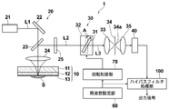
- FIG. 1 is a block diagram showing a schematic configuration of a Raman scattered light measurement apparatus 1 of the present embodiment.
- the Raman scattered light measurement apparatus 1 of the present embodiment has a photoelectric field enhancement substrate 10 that supports a subject S, and excitation light L1 from the back side of the photoelectric field enhancement substrate 10 to a subject placement location.
- An excitation light irradiation unit 20 that irradiates and a bandpass filter 31 on which Raman scattered light L2 emitted from the subject S and enhanced by the action of the photoelectric field enhancement substrate 10 is incident.
- the modulation unit 30 that performs frequency modulation on the Raman scattered light L2 by relatively scanning the peak wavelength peculiar to the subject S included in the Raman scattered light L2, and the modulation unit 30 performs frequency modulation.
- a light detector (corresponding to a light detector) 40 that detects the Raman scattered light L2 and outputs a light intensity signal, and obtains a temporal change in the light intensity signal output from the light detector 40; Take A lock-in amplifier 50 (corresponding to a signal acquisition unit) that acquires a signal having a frequency component higher than the modulation frequency of the frequency modulation based on the temporal change of the light intensity signal, and frequency modulation in the modulation unit 30
- a frequency setting unit 60 for setting the modulation frequency and a rotation control unit 70 for controlling the rotation drive unit 32 of the modulation unit 30 based on the modulation frequency set by the frequency setting unit 60 are provided.
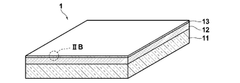
- FIG. 2A is a perspective view showing the photoelectric field enhancement substrate 10
- FIG. 2B is an enlarged view of a part IIB of the side surface of the photoelectric field enhancement substrate 10 shown in FIG. 2A.
- the photoelectric field enhancement substrate 10 is formed on a transparent substrate 11 made of glass or the like, a fine concavo-convex structure 12 formed on the surface of the transparent substrate 11, and a surface of the fine concavo-convex structure 12. And the metal film 13.
- the fine concavo-convex structure 12 in this embodiment is formed from boehmite.
- the fine concavo-convex structure 12 is formed so that the average depth and the average pitch of the convex portions of the metal fine concavo-convex structure when the metal film 13 is formed on the surface thereof are shorter than the wavelength of the excitation light L1.
- any material that can generate localized plasmons on the surface of the metal fine concavo-convex structure may be used.
- the average depth from the top of the convex portion to the bottom of the adjacent concave portion is 200 nm or less, and the average pitch between the vertices of the nearest adjacent convex portions separating the concave portions is 200 nm or less.
- the metal film 13 is formed along the surface of the fine concavo-convex structure 12, whereby the metal fine concavo-convex structure described above is formed.
- the photoelectric field enhancement substrate 10 can obtain a photoelectric enhancement effect by local plasmon resonance by this metal fine concavo-convex structure.
- the photoelectric field enhancement substrate 10 localized plasmon resonance is induced by irradiation of the excitation light L1 to the fine concavo-convex structure 12 (metal fine concavo-convex structure) on which the metal film 13 is formed. This generates an enhanced photoelectric field on the surface of the metal film 13.
- the metal film 13 only needs to be made of a metal that can generate localized plasmons when irradiated with the excitation light L1. It consists of at least one metal selected from the group consisting of: In particular, Au or Ag is preferable.
- the metal film 13 When the metal film 13 is formed on the surface of the fine concavo-convex structure 12, the metal film 13 has a concavo-convex shape that can generate localized plasmons when irradiated with the excitation light L ⁇ b> 1 as the metal fine concavo-convex structure.
- the thickness is preferably 10 nm to 100 nm.
- the excitation light irradiating unit 20 emits, for example, a semiconductor laser light source 21 (corresponding to an excitation light source) that emits excitation light L1 having a peak wavelength of 785 nm, and the excitation light L1 emitted from the semiconductor laser light source 21 to the photoelectric field enhancement substrate 10.
- a mirror 22 that reflects toward the photoelectric field, and includes the Raman scattered light L2 that is transmitted through the excitation light L1 reflected by the mirror 22 and is generated and enhanced in the subject S by irradiation of the excitation light L1.
- the half mirror 23 that reflects the light from the half mirror 23 and the excitation light L1 transmitted through the half mirror 23 to the region on the photoelectric field enhancement substrate 10 where the subject S is placed, and And a lens 24 for collimating light from the subject S side.
- a notch filter 25 is provided between the excitation light irradiation unit 20 and the modulation unit 30.
- the notch filter 25 removes the excitation light L1 from the light reflected by the half mirror 23 and transmits the other light.
- the modulation unit 30 includes a bandpass filter 31 on which the Raman scattered light L2 transmitted through the notch filter 25 is incident, and a rotation drive unit 32 that rotates the bandpass filter 31.
- the bandpass filter 31 of the present embodiment is an interference filter, and the center wavelength of the bandpass filter 31 is changed with respect to the incident Raman scattered light L2 by being rotated by the rotation driving unit 32.
- the band-pass filter 31 of the present embodiment includes the center wavelength of the band-pass filter 31 in the Raman scattered light L2 in a state where the Raman scattered light L2 is vertically incident on the light incident surface.
- the peak wavelength P ⁇ is unique to the subject S.
- the bandpass filter 31 is rotated by the rotation drive unit 32, and the rotation of the incident surface of the Raman scattered light L2 is changed by this rotation, whereby the band of the Raman scattered light L2 with respect to the peak wavelength P ⁇ is changed as shown in FIG.
- the center wavelength of the pass filter 31 is changed within the range of ⁇ .
- the bandpass filter 31 for example, when the peak wavelength P ⁇ of the Raman scattered light L2 is expected to be in the vicinity of 825 nm, the center wavelength of 830 nm at 0 degree incidence, the bandwidth of 1 nm, 5 degrees The change in the center wavelength of 820 nm to 830 nm is used.
- the bandwidth of the bandpass filter 31 is preferably smaller than the bandwidth of the peak wavelength unique to the subject S.
- FIG. 4 shows the Raman spectrum of the Raman scattered light L2, the peak wavelength P ⁇ specific to the subject S in the Raman spectrum, and the scanning range ⁇ of the center wavelength of the bandpass filter 31.
- a position where the light incident surface and the incident direction (optical axis direction) of the Raman scattered light L2 are perpendicular is a rotation initial position (dotted line position shown in FIG. 1).
- a rotation initial position dotted line position shown in FIG. 1
- the center wavelength of the bandpass filter 31 is reciprocally scanned within the scanning range ⁇ shown in FIGS. 3 and 4 by alternately repeating the clockwise rotation and the counterclockwise rotation of 5 degrees.
- the band-pass filter 31 is rotated by alternately repeating clockwise rotation and counterclockwise rotation of 180 degrees.
- the present invention is not limited thereto, and is specific to the subject S.
- Other rotation methods may be used as long as the peak wavelength P ⁇ transmits at least twice the transmission band of the bandpass filter 31.
- the bandpass filter 31 is rotated 360 degrees clockwise or counterclockwise. It may be.
- the rotation drive unit 32 rotates the band-pass filter 31 as described above, and includes, for example, a galvano motor.
- the rotation speed of the rotation drive unit 32 is controlled by the rotation control unit 70, and the rotation control unit 70 controls the rotation speed of the rotation drive unit 32 based on the frequency set in the frequency setting unit 60. It is.
- the frequency setting unit 60 sets the modulation frequency f of the frequency modulation in the modulation unit 30.
- the modulation frequency f is set by a user using a predetermined input unit (not shown).
- the rotation control unit 70 controls the rotation driving unit 32 so that the rotation speed becomes f (number of rotations / second), and the lock-in amplifier 50 2f signal is set to be detected. Note that one rotation in the present embodiment means that 180 degrees clockwise and counterclockwise are each performed once.
- a pinhole plate 34 provided with a pinhole 34a for removing noise light between the modulation unit 30 and the photodetector 40, and Raman scattered light L3 modulated by the modulation unit 30 to the pinhole 34a.
- a lens 33 for condensing light and a lens 35 for converting the modulated Raman scattered light L3 transmitted through the pinhole 34a into parallel light are provided.
- the photodetector 40 detects the modulated enhanced Raman scattered light L3 that is transmitted through the pinhole 34a and converted into parallel light by the lens 35, and outputs a light intensity signal corresponding to the detected light intensity. is there.
- the light detector 40 may be any device that photoelectrically converts incident light and outputs a light intensity signal as an electrical signal.
- the lock-in amplifier 50 receives the light intensity signal output from the photodetector 40, acquires a temporal change in the light intensity signal, and changes the temporal change in the acquired light intensity signal. Based on this, a signal having a frequency component higher than the modulation frequency f of the frequency modulation in the modulation unit 30 is acquired.
- the temporal change in the light intensity signal output from the photodetector 40 is shown in FIG. As shown. That is, a signal having a peak wavelength peculiar to the subject S that has passed through the bandpass filter 31 appears as a signal having a frequency component of 2f. Therefore, the lock-in amplifier 50 acquires a temporal change of the light intensity signal as shown in FIG. 5, and extracts and acquires a signal having a frequency component of 2f from the acquired light intensity signal. As a result, only a signal having a peak wavelength peculiar to the subject S can be accurately extracted.
- a predetermined subject S is placed on the metal film 13 of the photoelectric field enhancement substrate 10. Then, the pumping light L1 is emitted from the semiconductor laser light source 21 of the pumping light irradiation unit 20, and the pumping light L1 is reflected by the mirror 22 toward the photoelectric field enhancement substrate 10, passes through the half mirror 23, and is collected by the lens 24. Thus, the portion on the photoelectric field enhancement substrate 10 where the subject S is disposed is irradiated.
- the irradiation of the excitation light L1 induces localized plasmon resonance in the fine metal concavo-convex structure of the photoelectric field enhancement substrate 10, and an enhanced photoelectric field is generated on the surface of the metal film 13.
- the Raman scattered light L2 emitted from the subject S enhanced by the enhanced photoelectric field passes through the lens 24 and is reflected by the half mirror 23 toward the photodetector 40 side.
- the excitation light L1 reflected by the photoelectric field enhancement substrate 10 is also reflected by the half mirror 23 and reflected to the photodetector 40 side, but the excitation light L1 is removed by the notch filter 25.
- the Raman scattered light L2 transmitted through the notch filter 25 is incident on the bandpass filter 31 of the modulation unit 30.
- the band-pass filter 31 is rotated at a rotation speed f (number of rotations / second) by the rotation driving unit 32, and thereby the frequency modulation of the modulation frequency f is performed on the Raman scattered light L 2 incident on the band-pass filter 31. Applied.
- the Raman scattered light L3 frequency-modulated in the modulation unit 30 is collected by the lens 33, passes through the pinhole 34a, is converted into parallel light by the lens 35, and is incident on the photodetector 40.
- the modulated Raman scattered light L3 is detected by the photodetector 40, and a light intensity signal corresponding to the intensity of the light detected from the photodetector 40 is output and input to the lock-in amplifier 50.
- the lock-in amplifier 50 acquires a temporal change in the light intensity signal output from the photodetector 40, extracts a 2f frequency component signal from the acquired light intensity signal, and extracts the extracted signal.
- a signal having a peak wavelength peculiar to the subject S is output.
- the Raman scattered light L2 generated in the subject S by the irradiation of the excitation light L1 is incident on the bandpass filter 31, and the center wavelength of the bandpass filter 31 is measured.
- the Raman scattered light L2 is frequency-modulated by scanning with respect to the peak wavelength P ⁇ peculiar to the specimen S, and the time of the light intensity signal is detected by detecting the Raman scattered light L3 subjected to the frequency modulation. Since the change is acquired and the signal of the frequency component (2f) higher than the modulation frequency (f) of the frequency modulation is acquired based on the light intensity signal that changes with time, the spectrum is obtained as in the past.
- the signal of the high frequency component (2f) described above is detected while the Raman scattered light L2 is detected while the signal detection over the wide wavelength band by the detector is not performed. It is possible to extract as the signal, it is possible to achieve high-speed measurement.
- the signal of the high frequency component (2f) described above is extracted as a peak wavelength signal by frequency signal processing instead of conventional signal processing such as filter processing, a background signal is not included.
- the signal intensity at the peak wavelength can be obtained with high accuracy.
- the band pass filter 31 in the above embodiment may be configured to be detachable from the rotation drive unit 32. With this configuration, the band-pass filter 31 can be replaced and provided in the rotation drive unit 32 in accordance with the peak wavelength P ⁇ specific to various subjects S.
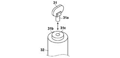
- FIG. 6 shows an example when the band-pass filter 31 is configured to be detachable from the rotation drive unit 32 as described above.
- the band pass filter 31 is provided with a rotating shaft 31a.
- a bearing attachment 31b that is configured to be detachable from the rotation drive unit 32 and to which the bandpass filter 31 can be attached and detached is provided.
- the bearing attachment 31b is formed with a hole 31c into which the rotary shaft 31a of the band pass filter 31 is fitted.
- the bearing attachment 31b is configured such that the rotation shaft 31a of the bandpass filter 31 is fitted in the hole 31c.
- Various band-pass filters 31 can be exchanged, and various band attachments 31b adjusted in accordance with the various band-pass filters 31 are attached to the rotary drive unit 32, which band-pass filter 31 is used. Even in this case, the bandpass filter 31 can be rotated with good balance.
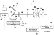
- FIG. 7 is a block diagram showing a schematic configuration of the Raman scattered light measurement apparatus 2 of the present embodiment.
- the Raman scattered light measurement apparatus 1 of the first embodiment described above and the Raman scattered light measurement apparatus 2 of the second embodiment differ in the configuration of the modulation unit.
- the Raman scattered light L2 emitted from the subject S is transmitted through the rotating bandpass filter 31 so as to modulate the frequency of the Raman scattered light.
- the bandpass filter 31 is fixed so that the Raman scattered light L2 is vertically incident, and the semiconductor laser light source 21 is controlled to control the semiconductor laser.
- the Raman scattered light L2 is modulated by changing the center wavelength of the excitation light L1 emitted from the light source 21.
- the Raman scattered light measurement apparatus 2 of the second embodiment is provided with a modulation unit 80 that controls the semiconductor laser light source 21 and scans the center wavelength of the excitation light L1. Yes.
- the center wavelength of the Raman scattered light L2 emitted from the subject S is also changed by the amount of movement of the center wavelength of the excitation light L1. .
- the bandpass filter 31 since the bandpass filter 31 is in a fixed state, the Raman scattered light L2 as shown in FIG. 8 with respect to the center wavelength of the band BW of the bandpass filter 31 is shown. Will be scanned.
- the peak wavelength of the Raman scattered light L2 is scanned in the range of ⁇ with the center wavelength of the band BW of the bandpass filter 31 as the center.
- This scanning range ⁇ is the same range as the scanning range ⁇ shown in FIG. 3 in the first embodiment. That is, in the first embodiment, the Raman scattered light L2 is modulated by scanning the center wavelength of the bandpass filter 31 with respect to the peak wavelength of the Raman scattered light L2. In the embodiment, conversely, the Raman scattered light L2 is modulated by scanning the center wavelength of the Raman scattered light L2 with respect to the center wavelength of the bandpass filter 31.
- the frequency f set by the frequency setting unit 60 is output to the modulation unit 80, and the modulation unit 80 is configured to perform the rotation of the bandpass filter 31 in the first embodiment, that is, during 1 / f time.
- the semiconductor laser light source 21 is controlled so that the peak wavelength of the Raman scattered light L2 is scanned twice in the scanning range ⁇ shown in FIG.
- the modulated Raman scattered light L2 transmitted through the bandpass filter 31 is detected by the photodetector 40 as in the first embodiment, and the light intensity signal output from the photodetector 40 is sent to the lock-in amplifier 50. Even in the second embodiment, the temporal change of the light intensity signal as shown in FIG. 5 is acquired by the lock-in amplifier 50 in the second embodiment.
- the temporal change of the light intensity signal output from the photodetector 40 is acquired by the lock-in amplifier 50, and the lock-in is performed.
- the amplifier 50 acquires a signal having a frequency component of 2f, which is twice the modulation frequency f.
- the high-pass filter processing unit 100 uses the temporal signal of the light intensity signal. You may make it acquire a change.
- the high-pass filter processing unit 100 performs high-pass filter processing for cutting a signal having a frequency component equal to or lower than the modulation frequency f and transmitting a signal having a frequency component of 2f.
- the high-pass filter may be configured by hardware or software.
- the center of the scanning range ⁇ is the center wavelength of the Raman scattered light L2, and in the Raman scattered light measuring apparatus 2 of the second embodiment, the scanning range.
- the center of ⁇ is not necessarily set as described above, and the center of the scanning range ⁇ may be shifted from the center wavelength of the Raman scattered light L2 or the center wavelength of the bandpass filter 31. In this case, a signal having a frequency component other than 2f appears in the temporal change in the light intensity signal detected by the photodetector 40.
- the frequency of this signal is always higher than the modulation frequency f. Therefore, a signal having the desired frequency may be acquired. In this case, since signals of a plurality of types of frequencies are included, it is preferable to detect the signal by the high-pass filter processing unit 100 described above.
- the subject S is scanned two-dimensionally with the excitation light L1, and each scanning point of the excitation light L1 on the subject S is scanned.
- the temporal change of the light intensity signal is acquired, and the frequency component (2f) higher than the modulation frequency (f) of the frequency modulation is obtained based on the temporal change of the acquired light intensity signal.
- the photoelectric field enhancement substrate 10 is held, and the X direction and Y direction (paper thickness) shown in FIG.
- a moving stage 200 for moving the photoelectric field enhancement substrate 10 is provided in the direction of the vertical direction, and the photoelectric field enhancement substrate 10 is moved by the movement stage 200, so that the object S on the photoelectric field enhancement substrate 10 is moved by 2 with the excitation light L1. You may make it scan in a dimensional form.
- the configuration for scanning the excitation light L1 in a two-dimensional manner is not limited to this, and the photoelectric field enhancement substrate 10 is fixed, and the object S is two-dimensionally driven by the excitation light L1 by using, for example, a galvanomirror. You may make it scan in a shape.
- the subject S can be scanned two-dimensionally with the excitation light L1 by using the same configuration as described above.
- the excitation light irradiation unit 20 is disposed on the front surface side (subject placement surface side) of the photoelectric field enhancement substrate 10 and the excitation light L1 is irradiated from the front surface side of the photoelectric field enhancement substrate 10. Also good. With respect to the metal fine uneven structure of the photoelectric field enhancement substrate 10, localized plasmon resonance can be similarly induced regardless of whether the excitation light L1 is incident from either of the front and back sides, and a photoelectric field enhancement effect can be obtained.
- the fine concavo-convex structure 12 of the photoelectric field enhancing substrate 10 is made of boehmite, but may be made of a transparent material other than boehmite.
- an anodized alumina layer having a large number of micropores in an upper layer portion is prepared by anodizing an aluminum substrate, and an anodized alumina layer from which an anodized aluminum portion is removed is formed into a fine relief structure 12. And this may be fixed on the transparent substrate 11.
- the fine concavo-convex structure is not limited to one made of a material different from that of the transparent substrate, but may be made of the same material as the substrate by processing the surface of the transparent substrate. For example, you may use what formed the fine concavo-convex structure on the surface by carrying out the lithography and dry etching process of the surface of a glass substrate.
Landscapes
- Physics & Mathematics (AREA)
- Spectroscopy & Molecular Physics (AREA)
- General Physics & Mathematics (AREA)
- Health & Medical Sciences (AREA)
- Nuclear Medicine, Radiotherapy & Molecular Imaging (AREA)
- Life Sciences & Earth Sciences (AREA)
- Chemical & Material Sciences (AREA)
- Analytical Chemistry (AREA)
- Biochemistry (AREA)
- General Health & Medical Sciences (AREA)
- Immunology (AREA)
- Pathology (AREA)
- Investigating, Analyzing Materials By Fluorescence Or Luminescence (AREA)
Description
本発明は、被検体に特有のピーク波長を有するラマン散乱光を測定するラマン散乱光測定装置および方法に関するものである。
従来、被検体を構成する物質の同定などを行う方法としてラマン分光法が提案されている。ラマン分光法は、物質に単波長光を照射して得られる散乱光を分光して、ラマン散乱光のスペクトル(ラマンスペクトル)を得る方法であり、このスペクトルのピーク波長を解析することによって物質の同定などを行うことができる。
上述したラマン分光法としては、微弱なラマン散乱光を増強するため、局在プラズモン共鳴によって増強された光電場を利用した、いわゆる表面増強ラマン(SERS)と呼ばれる方法がある(特許文献1、非特許文献1~3参照)。
この方法は、金属体、特に表面にナノオーダの凹凸を有する金属体に物質を接触させた状態で光を照射すると、局在プラズモン共鳴による光電場増強が生じ、金属体表面に接触された試料のラマン散乱光の強度が増強されるという原理を利用したものである。被検体を担持する担体(基板)として、表面に金属凹凸構造を備えた基板を用いることにより表面増強ラマン分光法を実施することができる。
戸田、半那、谷著、日本写真学会誌 70,38(2007)
Optics Express, Vol.17, No.21, 18556
Nano Letters, Vol.19, No.6, 2343
ここで、上述したようなラマン分光法においては、被検体からのラマン散乱光だけでなく、基板から発せられた蛍光も分光器によって検出されることになるので、分光器によって検出される信号には、図4に示すように、ラマン散乱光のピーク波長だけでなく、広い波長帯域に亘るバックグラウンドの信号が含まれることになる。
したがって、従来は、このバックグラントを含むスペクトルの信号に対して、たとえばフィルタ処理などの信号処理を施すことによってピーク波長の信号を抽出するようにしていたが、フィルタ処理による信号抽出には精度に限界があり、高精度にピーク波長の信号を抽出することが困難であった。
また、上述したような信号処理によってピーク波長の信号を抽出する場合には、分光器によって広い波長帯域に亘って信号検出した後にピーク波長の信号抽出が行われるため、そのピーク波長の信号抽出までに要する時間が長くなるという問題がある。特に、基板上に設置された被検体に対して2次元状に光を走査し、各走査点についてピーク波長の信号を取得するような場合には、各走査点について広い波長帯域に亘る信号検出を行う必要があるため、全ての走査点についてピーク波長の信号抽出が終了するまでに、かなりの時間を要するという問題がある。たとえば15mm×20mmの範囲を数100μmのピッチで光を走査する際、1つの走査点について1秒の時間を要するとすると、全ての走査点について信号抽出を終了するまでに数時間を要することになる。
本発明は、上記事情に鑑み、ラマン散乱光の測定をしながら高速にピーク波長の信号を検出できるとともに、高精度にピーク波長の信号を抽出することができるラマン散乱光測定装置および方法を提供することを目的とする。
本発明のラマン散乱光測定装置は、被検体に対して励起光を照射する励起光照射部と、励起光の照射によって被検体において発生したラマン散乱光が入射されるバンドパスフィルタを有し、そのバンドパスフィルタの中心波長とラマン散乱光に含まれる被検体に特有のピーク波長とを、そのピーク波長がバンドパスフィルタの帯域を少なくとも2回透過する範囲で相対的に走査することによってラマン散乱光に対して周波数変調を施す変調部と、周波数変調が施されたラマン散乱光を検出して光強度信号を出力する光検出部と、光強度信号の時間的な変化を取得し、その取得した光強度信号の時間的な変化に基づいて、周波数変調の変調周波数よりも高い周波数成分の信号を取得する信号取得部とを備えたことを特徴とする。
また、上記本発明のラマン散乱光測定装置においては、変調部を、バンドパスフィルタを回転させる回転駆動部を有するものとし、回転駆動部によりバンドパスフィルタを回転させることによってバンドパスフィルタの中心波長を変更して上記走査を行うものとできる。
また、バンドパスフィルタを、回転駆動部に対して着脱可能に構成することができる。
また、バンドパスフィルタが着脱可能に設置され、その設置されたバンドパスフィルタを支持する支持部材を有するものとし、支持部材を、回転駆動部に対して着脱可能に構成することができる。
また、変調部を、励起光を射出する励起光源を制御することによって励起光の中心波長を変更して上記走査を行うものとできる。
また、励起光源として、半導体レーザ光源を用いることができる。
また、信号取得部を、ロックインアンプを有するものとし、そのロックインアンプを用いて変調周波数よりも高い周波数成分の信号を取得することができる。
また、信号取得部を、変調周波数以下の周波数成分の信号を除去するハイパスフィルタを有するものとし、そのハイパスフィルタを用いて変調周波数よりも高い周波数成分の信号を取得することができる。
また、信号取得部を、変調周波数の2倍の周波数成分の信号を取得するものとできる。
また、励起光によって被検体上が2次元状に走査されるものとし、信号取得部を、被検体上の励起光の各走査点について、光強度信号の時間的な変化を取得し、その取得した光強度信号の時間的な変化に基づいて、周波数変調の変調周波数よりも高い周波数成分の信号を取得するものとできる。
また、透明な微細凹凸構造を備えた透明基板と、前記微細凹凸構造表面に形成された金属膜とを備えた光電場増強デバイスを有するものとし、励起光照射部を、光電場増強デバイスの金属膜上に配置された被検体に対して励起光を照射するものとできる。
本発明のラマン散乱光測定方法は、被検体に対して励起光を照射し、その励起光の照射によって被検体において発生したラマン散乱光をバンドパスフィルタに入射させ、かつそのバンドパスフィルタの中心波長とラマン散乱光に含まれる被検体に特有のピーク波長とを、そのピーク波長がバンドパスフィルタの帯域を少なくとも2回透過する範囲で相対的に走査することによってラマン散乱光に対して周波数変調を施し、その周波数変調が施されたラマン散乱光を検出することによって光強度信号の時間的な変化を取得し、その時間的に変化する光強度信号に基づいて、周波数変調の変調周波数よりも高い周波数成分の信号を取得することを特徴とする。
本発明のラマン散乱光測定装置および方法によれば、被検体に対して励起光を照射し、その励起光の照射によって被検体において発生したラマン散乱光をバンドパスフィルタに入射させ、かつそのバンドパスフィルタの中心波長とラマン散乱光に含まれる被検体に特有のピーク波長とを、そのピーク波長がバンドパスフィルタの帯域を少なくとも2回透過する範囲で相対的に走査することによってラマン散乱光に対して周波数変調を施し、その周波数変調が施されたラマン散乱光を検出することによって光強度信号の時間的な変化を取得し、その時間的に変化する光強度信号に基づいて、周波数変調の変調周波数よりも高い周波数成分の信号を取得するようにしたので、従来のように、分光器による広い波長帯域に亘る信号検出を行う必要がなく、ラマン散乱光の検出を行いながら上述した高い周波数成分の信号をピーク波長の信号として抽出することができるので、高速な測定を実現することができる。
また、従来のようなフィルタ処理などの信号処理ではなく、周波数信号処理によって上述した高い周波数成分の信号をピーク波長の信号として抽出するようにしたので、バックグラウンドの信号を含むことなく、ピーク波長の信号強度を高精度に抽出することができる。
以下、本発明のラマン散乱光測定装置および方法の第1の実施形態について、図面を参照しながら詳細に説明する。図1は、本実施形態のラマン散乱光測定装置1の概略構成を示すブロック図である。
本実施形態のラマン散乱光測定装置1は、図1に示すように、被検体Sを支持する光電場増強基板10と、光電場増強基板10の裏面側から被検体配置箇所へ励起光L1を照射する励起光照射部20と、被検体Sから発せられ光電場増強基板10の作用により増強されたラマン散乱光L2が入射されるバンドパスフィルタ31を有し、そのバンドパスフィルタ31の中心波長とラマン散乱光L2に含まれる被検体Sに特有のピーク波長とを相対的に走査することによってラマン散乱光L2に対して周波数変調を施す変調部30と、変調部30によって周波数変調の施されたラマン散乱光L2を検出して光強度信号を出力する光検出器(光検出部に相当する)40と、光検出器40から出力された光強度信号の時間的な変化を取得し、その取得した光強度信号の時間的な変化に基づいて、上記周波数変調の変調周波数よりも高い周波数成分の信号を取得するロックインアンプ50(信号取得部に相当する)と、変調部30における周波数変調の変調周波数が設定される周波数設定部60と、周波数設定部60において設定された変調周波数に基づいて、変調部30の回転駆動部32を制御する回転制御部70とを備えている。
まず、光電場増強基板10について説明する。図2Aは、光電場増強基板10を示す斜視図であり、図2Bは、図2Aに示した光電場増強基板10の側面の一部IIBの拡大図である。
光電場増強基板10は、図2Aおよび図2Bに示すように、ガラスなどからなる透明基板11と、透明基板11の表面に形成された微細凹凸構造12と、微細凹凸構造12の表面に形成された金属膜13とからなるものである。
本実施形態における微細凹凸構造12は、ベーマイトから形成されるものである。微細凹凸構造12は、その表面に金属膜13を形成した場合の金属微細凹凸構造の凸部の深さの平均およびピッチの平均が、励起光L1の波長より短くなるように形成されるものであるが、金属微細凹凸構造の表面に局在プラズモンを生じさせうるものであればよい。特に、微細凹凸構造12は、凸部頂点から隣接する凹部の底部までの深さの平均が200nm以下、凹部を隔てた最隣接凸部の頂点同士のピッチの平均が200nm以下であることが望ましい。
金属膜13は、微細凹凸構造12の表面に沿って形成されるものであり、これにより上述した金属微細凹凸構造が形成される。そして、光電場増強基板10は、この金属微細凹凸構造によって局在プラズモン共鳴による光電増強効果を得ることができるものである。
具体的には、光電場増強基板10は、金属膜13が形成された微細凹凸構造12(金属微細凹凸構造)への励起光L1の照射によって局在プラズモン共鳴が誘起され、この局在プラズモン共鳴により金属膜13の表面に増強された光電場を生じさせるものである。
金属膜13は、励起光L1の照射を受けて局在プラズモンを生じうる金属からなるものであればよいが、例えば、Au、Ag、Cu、Al、Pt、およびこれらを主成分とする合金からなる群より選択される少なくとも1種の金属からなるものである。特には、AuあるいはAgが好ましい。
金属膜13の膜厚は、金属膜13が微細凹凸構造12の表面に形成された場合に、金属微細凹凸構造として励起光L1の照射を受けて局在プラズモンを生じうる凹凸形状を維持することができる程度の厚みであれば特に制限はないが、10nm~100nmであることが好ましい。
励起光照射部20は、たとえばピーク波長785nmの励起光L1を射出する半導体レーザ光源21(励起光源に相当する)と、この半導体レーザ光源21から射出された励起光L1を光電場増強基板10に向けて反射するミラー22と、そのミラー22により反射された励起光L1を透過し、かつ励起光L1の照射により被検体Sにおいて発生し増強されたラマン散乱光L2を含む光電場増強基板10側からの光を、光検出器40に向けて反射するハーフミラー23と、ハーフミラー23を透過した励起光L1を光電場増強基板10の被検体Sが載置された領域に集光し、かつ被検体S側からの光を平行光化するレンズ24とを備えている。
励起光照射部20と変調部30との間には、ノッチフィルタ25が設けられている。ノッチフィルタ25は、ハーフミラー23により反射された光のうち励起光L1を除去し、それ以外の光を透過するものである。
変調部30は、ノッチフィルタ25を透過したラマン散乱光L2が入射されるバンドパスフィルタ31と、バンドパスフィルタ31を回転させる回転駆動部32とを備えている。本実施形態のバンドパスフィルタ31は干渉フィルタであって、回転駆動部32によって回転させられることによって、入射されるラマン散乱光L2に対してその中心波長が変化するものである。
具体的には、本実施形態のバンドパスフィルタ31は、その光入射面に対してラマン散乱光L2が垂直に入射する位置に配置された状態において、その中心波長がラマン散乱光L2に含まれる被検体Sに特有のピーク波長Pλとなるように構成されたものである。
そして、バンドパスフィルタ31は、回転駆動部32によって回転し、この回転によってラマン散乱光L2の入射面の傾きが変更され、これにより図3に示すようにラマン散乱光L2のピーク波長Pλに対するバンドパスフィルタ31の中心波長がΔλの範囲で変更されるものである。具体的には、バンドパスフィルタ31としては、たとえばラマン散乱光L2のピーク波長Pλが825nm近傍であると予想される場合には、0度入射で830nmの中心波長、1nmの帯域幅、5度の角度変化で820nm~830nmの中心波長変化のものが用いられる。なお、バンドパスフィルタ31の帯域幅は、被検体Sに特有のピーク波長の帯域幅よりも小さい方がよい。図4は、ラマン散乱光L2のラマンスペクトルと、そのラマンスペクトルにおける被検体Sに特有のピーク波長Pλと、バンドパスフィルタ31の中心波長の走査範囲Δλを示すものである。
本実施形態におけるバンドパスフィルタ31は、その光入射面とラマン散乱光L2の入射方向(光軸方向)とが垂直になる位置を回転初期位置(図1に示す点線位置)とし、図1において矢印Aで示すように、その回転初期位置から時計回りに5度回転した後、反時計回りに回転して回転初期位置に一旦戻った後、さらにその回転初期位置から反時計回りに5度回転し、その後、再び時計回りに回転して回転初期位置に戻る。そして、この5度の時計回りと反時計回りとが交互に繰り返されることによって、バンドパスフィルタ31の中心波長が、図3および図4に示す走査範囲Δλで往復走査される。なお、本実施形態においては、上述したように180度の時計回りと反時計回りとを交互に繰り返してバンドパスフィルタ31を回転させるようにしたが、これに限らず、被検体Sに特有のピーク波長Pλが、バンドパスフィルタ31の透過帯域を少なくとも2回透過するような回転方法であればその他の回転方法でもよく、たとえばバンドパスフィルタ31を360度時計回りまたは反時計回りに回転させるようにしてもよい。
回転駆動部32は、バンドパスフィルタ31を上述したように回転させるものであり、たとえばガルバノモータなどから構成されるものである。
回転駆動部32の回転速度は、回転制御部70によって制御されるものであり、回転制御部70は、周波数設定部60において設定された周波数に基づいて回転駆動部32の回転速度を制御するものである。
周波数設定部60は、変調部30における周波数変調の変調周波数fが設定されるものである。この変調周波数fは、ユーザによって所定の入力部(図示省略)を用いて設定される。そして、周波数設定部60に周波数fが設定された場合、回転制御部70は、回転速がf(回転数/秒)となるように回転駆動部32を制御し、ロックインアンプ50は、周波数2fの信号を検出するように設定される。なお、本実施形態でいう1回転とは、180度の時計回りと反時計回りとがそれぞれ1回行われることをいう。
変調部30と光検出器40との間には、ノイズ光を除去するためのピンホール34aが設けられたピンホール板34と、変調部30によって変調後のラマン散乱光L3をピンホール34aへ集光するためのレンズ33と、ピンホール34aを透過した変調後のラマン散乱光L3を平行光化するレンズ35とが設けられている。
光検出器40は、ピンホール34aを透過し、レンズ35によって平行光化された変調後の増強ラマン散乱光L3を検出し、その検出した光の強度に応じた光強度信号を出力するものである。光検出器40としては、入射した光を光電変換して電気信号としての光強度信号を出力するものであれば如何なるものでもよい。
ロックインアンプ50は、光検出器40から出力された光強度信号が入力されるものであり、その光強度信号の時間的な変化を取得し、その取得した光強度信号の時間的な変化に基づいて、変調部30における周波数変調の変調周波数fよりも高い周波数成分の信号を取得するものである。
具体的には、上述したようにバンドパスフィルタ31の回転速度をf(回転数/秒)に設定した場合、光検出器40から出力される光強度信号の時間的な変化は、図5に示すようなものとなる。すなわち、バンドパスフィルタ31を透過した被検体Sに特有のピーク波長の信号が2fの周波数成分の信号として現れることになる。したがって、ロックインアンプ50は、図5に示すような光強度信号の時間的な変化を取得し、その取得した光強度信号から2fの周波数成分の信号を抽出して取得するものである。これにより被検体Sに特有のピーク波長の信号のみを精度よく抽出することができる。
次に、本実施形態のラマン散乱光測定装置1を用いたラマン散乱光のピーク波長の測定方法について説明する。
まず、光電場増強基板10の金属膜13上に所定の被検体Sが設置される。そして、励起光照射部20の半導体レーザ光源21から励起光L1が射出され、励起光L1はミラー22において光電場増強基板10側に反射され、ハーフミラー23を透過してレンズ24によって集光されて、光電場増強基板10上の被検体Sが配置された箇所に照射される。
励起光L1の照射により、光電場増強基板10の金属微細凹凸構造において局在プラズモン共鳴が誘起され、金属膜13表面に増強された光電場が生じる。この増強光電場により増強された、被検体Sから発せられたラマン散乱光L2は、レンズ24を透過して、ハーフミラー23で光検出器40側に反射される。なお、このとき、光電場増強基板10で反射された励起光L1もハーフミラー23により反射されて光検出器40側に反射されるが、励起光L1はノッチフィルタ25で除去される。
そして、ノッチフィルタ25を透過したラマン散乱光L2は、変調部30のバンドパスフィルタ31に入射される。このときバンドパスフィルタ31は、回転駆動部32によって回転速度f(回転数/秒)で回転し、これによりバンドパスフィルタ31に入射されたラマン散乱光L2に対して変調周波数fの周波数変調が施される。
そして、変調部30において周波数変調の施されたラマン散乱光L3はレンズ33によって集光され、ピンホール34aを透過した後、レンズ35によって平行光化され、光検出器40へ入射される。
変調後のラマン散乱光L3は、光検出器40によって検出され、光検出器40から検出した光の強度に応じた光強度信号が出力され、ロックインアンプ50に入力される。ロックインアンプ50は、光検出器40から出力された光強度信号の時間的な変化を取得し、その取得した光強度信号の中から2fの周波数成分の信号を抽出し、その抽出した信号を被検体Sに特有のピーク波長の信号として出力する。
上記実施形態のラマン散乱光測定装置1によれば、励起光L1の照射によって被検体Sにおいて発生したラマン散乱光L2をバンドパスフィルタ31に入射させ、かつそのバンドパスフィルタ31の中心波長を被検体Sに特有のピーク波長Pλに対して走査することによってラマン散乱光L2に対して周波数変調を施し、その周波数変調が施されたラマン散乱光L3を検出することによって光強度信号の時間的な変化を取得し、その時間的に変化する光強度信号に基づいて、周波数変調の変調周波数(f)よりも高い周波数成分(2f)の信号を取得するようにしたので、従来のように、分光器による広い波長帯域に亘る信号検出を行う必要がなく、ラマン散乱光L2の検出を行いながら上述した高い周波数成分(2f)の信号をピーク波長の信号として抽出することができるので、高速な測定を実現することができる。
また、従来のようなフィルタ処理などの信号処理ではなく、周波数信号処理によって上述した高い周波数成分(2f)の信号をピーク波長の信号として抽出するようにしたので、バックグラウンドの信号を含むことなく、ピーク波長の信号強度を高精度に取得することができる。
また、上記実施形態におけるバンドパスフィルタ31を、回転駆動部32に着脱可能に構成するようにしてもよい。このように構成することによって、種々の被検体Sに特有のピーク波長Pλに応じてバンドパスフィルタ31を交換して回転駆動部32に設けることができる。
図6は、上述したようにバンドパスフィルタ31を回転駆動部32に対して着脱可能に構成した場合の一例を示すものである。バンドパスフィルタ31には回転軸31aが設けられている。一方、回転駆動部32側には、回転駆動部32に対して着脱可能に構成されるとともに、バンドパスフィルタ31を着脱可能な軸受けアタッチメント31bが設けられている。この軸受けアタッチメント31bには、バンドパスフィルタ31の回転軸31aが嵌合する穴31cが形成されている。そして、軸受けアタッチメント31bは、その穴31cにバンドパスフィルタ31の回転軸31aが嵌合されるものであり、回転駆動部32によってバンドパスフィルタ31が回転した際、バンドパスフィルタ31がその回転中心がぶれることなくバランス良く回転するようにバランス調整されて構成されている。
種々のバンドパスフィルタ31を交換可能にするともに、その種々のバンドパスフィルタ31に応じてバランス調整された種々の軸受けアタッチメント31bを回転駆動部32に取り付けることによって、どのバンドパスフィルタ31を用いた場合でも、そのバンドパスフィルタ31をバランス良く回転させることができる。
次に、本発明のラマン散乱光測定装置および方法の第2の実施形態について説明する。図7は、本実施形態のラマン散乱光測定装置2の概略構成を示すブロック図である。上述した第1の実施形態のラマン散乱光測定装置1と第2の実施形態のラマン散乱光測定装置2とは変調部の構成が異なる。
第1の実施形態のラマン散乱光測定装置1においては、被検体Sから発せられたラマン散乱光L2を回転するバンドパスフィルタ31に透過させることによってラマン散乱光に対して周波数変調を施すようにしたが、第2の実施形態のラマン散乱光測定装置2においては、バンドパスフィルタ31をラマン散乱光L2が垂直に入射するように固定された状態とし、半導体レーザ光源21を制御して半導体レーザ光源21から射出される励起光L1の中心波長を変更することによってラマン散乱光L2に変調を施すものである。
具体的には、第2の実施形態のラマン散乱光測定装置2は、図7に示すように、半導体レーザ光源21を制御して励起光L1の中心波長を走査する変調部80が設けられている。
ここで、上述したように励起光L1の中心波長を変更した場合、被検体Sから発せられたラマン散乱光L2の中心波長も励起光L1の中心波長の移動した量だけ変更されることになる。
そして、上述したように本実施形態においては、バンドパスフィルタ31は固定された状態であるので、そのバンドパスフィルタ31の帯域BWの中心波長に対して、図8に示すようにラマン散乱光L2のピーク波長が走査されることになる。
本実施形態においては、バンドパスフィルタ31の帯域BWの中心波長を中心としてΔλの範囲でラマン散乱光L2のピーク波長が走査されるものとする。この走査範囲Δλは、第1の実施形態における図3に示した走査範囲Δλと同じ範囲である。すなわち、第1の実施形態においては、ラマン散乱光L2のピーク波長に対してバンドパスフィルタ31の中心波長を走査することによってラマン散乱光L2に対して変調を施すようにしたが、第2の実施形態においては、逆にバンドパスフィルタ31の中心波長に対してラマン散乱光L2の中心波長を走査することによってラマン散乱光L2に対して変調を施すようにしたものである。
そして、周波数設定部60において設定された周波数fが変調部80に出力され、変調部80は、上記第1の実施形態においてバンドパスフィルタ31が1回転する時間、すなわち1/f時間の間に、図8に示す走査範囲Δλをラマン散乱光L2のピーク波長が2回走査されるように半導体レーザ光源21を制御する。
バンドパスフィルタ31を透過した変調後のラマン散乱光L2は、第1の実施形態と同様に、光検出器40によって検出され、光検出器40から出力された光強度信号がロックインアンプ50に入力されることになるが、第2の実施形態においても、図5に示すような光強度信号の時間的な変化がロックインアンプ50によって取得されることになる。
なお、その他、図7において上記第1の実施形態と同じ符号を示した構成要素については、上記第1の実施形態と同様である。
また、上記第1および第2の実施形態のラマン散乱光測定装置1,2においては、光検出器40から出力された光強度信号の時間的な変化をロックインアンプ50によって取得し、ロックインアンプ50によって変調周波数fの2倍の周波数である2fの周波数成分の信号を取得するようにしたが、図9および図10に示すように、ハイパスフィルタ処理部100によって光強度信号の時間的な変化を取得するようにしてもよい。ハイパスフィルタ処理部100は、変調周波数f以下の周波数成分の信号をカットし、2fの周波数成分の信号を透過させるハイパスフィルタ処理を施すものである。ハイパスフィルタは、ハードウェアで構成するようにしてもよいし、ソフトウェアで構成するようにしてもよい。
また、上記第1の実施形態のラマン散乱光測定装置1においては、走査範囲Δλの中心をラマン散乱光L2の中心波長とし、第2の実施形態のラマン散乱光測定装置2においては、走査範囲Δλの中心をバンドパスフィルタ31の中心波長とすることによって、光検出器40によって検出される光強度信号の時間的な変化の中に2fの周波数成分の信号が現れるようにしたが、走査範囲Δλは必ずしも上記のように設定する必要はなく、走査範囲Δλの中心が、ラマン散乱光L2の中心波長やバンドパスフィルタ31の中心波長からずれていてもよい。この場合、光検出器40によって検出される光強度信号の時間的な変化の中に2f以外の周波数成分の信号が現れることになるが、この信号の周波数は、必ず変調周波数fよりも高い所望の周波数となるので、その所望の周波数の信号を取得するようにすれば良い。この場合、複数種類の周波数の信号が含まれることになるので、上述したハイパスフィルタ処理部100によって信号検出することが好ましい。
また、上記第1および第2の実施形態のラマン散乱光測定装置1,2において、励起光L1によって被検体S上を2次元状に走査し、被検体S上の励起光L1の各走査点について、上述したように光強度信号の時間的な変化を取得し、その取得した光強度信号の時間的な変化に基づいて、周波数変調の変調周波数(f)よりも高い周波数成分(2f)の信号をピーク波長の信号としてそれぞれ取得するようにしてもよい。
具体的には、たとえば、図11に示すように、第1の実施形態のラマン散乱光測定装置1において、光電場増強基板10を保持するとともに、図11に示すX方向およびY方向(紙面厚さ方向)に光電場増強基板10を移動させる移動ステージ200を設け、この移動ステージ200によって光電場増強基板10を移動させることによって、光電場増強基板10の被検体S上を励起光L1によって2次元状に走査するようにしてもよい。
なお、励起光L1を2次元状に走査する構成としてはこれに限らず、光電場増強基板10は固定した状態とし、たとえばガルバノミラーなどを用いることによって被検体S上を励起光L1によって2次元状に走査するようにしてもよい。
また、第2の実施形態のラマン散乱光測定装置2においても、上記と同様の構成を用いることにより励起光L1によって被検体S上を2次元状に走査することができる。
また、上記第1および第2の実施形態においては、励起光照射部20を光電場増強基板10の裏面側に配置し、光電場増強基板10の裏面側から励起光L1を照射する構成であるが、これに限らず、励起光照射部20を、光電場増強基板10の表面側(被検体配置面側)に配置し、光電場増強基板10の表面側から励起光L1を照射する構成としてもよい。光電場増強基板10の金属微細凹凸構造に対しては、表裏のいずれから励起光L1が入射されても同様に局在プラズモン共鳴を誘起することができ、光電場増強効果を得ることができる。
また、上記第1および第2の実施形態においては、光電場増強基板10の微細凹凸構造12は、ベーマイトにより構成されるものとしたが、ベーマイト以外の透明な材料により構成されていてもよい。例えば、アルミニウム基体に対して、陽極酸化処理を施してその上層部に多数の微細孔を有する陽極酸化アルミナを作製し、陽極酸化されていないアルミニウム部分を除去した陽極酸化アルミナ層を微細凹凸構造12とし、これを透明基板11上に固定してもよい。
また、微細凹凸構造は透明基板と異なる材料により構成されたもののみならず、透明基板の表面を加工することにより基板と同一の材料により構成されていてもよい。例えば、ガラス基板の表面をリソグラフィーとドライエッチング処理することにより、表面に微細凹凸構造を形成したものを用いてもよい。
Claims (12)
- 被検体に対して励起光を照射する励起光照射部と、
前記励起光の照射によって前記被検体において発生したラマン散乱光が入射されるバンドパスフィルタを有し、該バンドパスフィルタの中心波長と前記ラマン散乱光に含まれる前記被検体に特有のピーク波長とを、該ピーク波長が前記バンドパスフィルタの帯域を少なくとも2回透過する範囲で相対的に走査することによって前記ラマン散乱光に対して周波数変調を施す変調部と、
前記周波数変調が施されたラマン散乱光を検出して光強度信号を出力する光検出部と、
前記光強度信号の時間的な変化を取得し、該取得した光強度信号の時間的な変化に基づいて、前記周波数変調の変調周波数よりも高い周波数成分の信号を取得する信号取得部とを備えたことを特徴とするラマン散乱光測定装置。 - 前記変調部が、前記バンドパスフィルタを回転させる回転駆動部を有し、該回転駆動部により前記バンドパスフィルタを回転させることによって該バンドパスフィルタの中心波長を変更して前記走査を行うものであることを特徴とする請求項1記載のラマン散乱光測定装置。
- 前記バンドパスフィルタが、前記回転駆動部に対して着脱可能に構成されたものであることを特徴とする請求項2記載のラマン散乱光測定装置。
- 前記バンドパスフィルタが着脱可能に設置され、該設置されたバンドパスフィルタを支持する支持部材を有し、
該支持部材が、前記回転駆動部に対して着脱可能に構成されたものであることを特徴とする請求項3記載のラマン散乱光測定装置。 - 前記変調部が、前記励起光を射出する励起光源を制御することによって前記励起光の中心波長を変更して前記走査を行うものであることを特徴とする請求項1記載のラマン散乱光測定装置。
- 前記励起光源が、半導体レーザ光源であることを特徴とする請求項5記載のラマン散乱光測定装置。
- 前記信号取得部が、ロックインアンプを有し、
該ロックインアンプを用いて前記変調周波数よりも高い周波数成分の信号を取得するものであることを特徴とする請求項1から6いずれか1項記載のラマン散乱光測定装置。 - 前記信号取得部が、前記変調周波数以下の周波数成分の信号を除去するハイパスフィルタを有し、
該ハイパスフィルタを用いて前記変調周波数よりも高い周波数成分の信号を取得するものであることを特徴とする請求項1から6いずれか1項記載のラマン散乱光測定装置。 - 前記信号取得部が、前記変調周波数の2倍の周波数成分の信号を取得するものであることを特徴とする請求項1から8いずれか1項記載のラマン散乱光測定装置。
- 前記励起光によって前記被検体上が2次元状に走査され、
前記信号取得部が、前記被検体上の前記励起光の各走査点について、前記光強度信号の時間的な変化を取得し、該取得した光強度信号の時間的な変化に基づいて、前記周波数変調の変調周波数よりも高い周波数成分の信号を取得するものであることを特徴とする請求項1から9いずれか1項記載のラマン散乱光測定装置。 - 透明な微細凹凸構造を備えた透明基板と、前記微細凹凸構造表面に形成された金属膜とを備えた光電場増強デバイスを有し、
前記励起光照射部が、前記光電場増強デバイスの前記金属膜上に配置された被検体に対して前記励起光を照射するものであることを特徴とする請求項1から10いずれか1項記載のラマン散乱光測定装置。 - 被検体に対して励起光を照射し、
該励起光の照射によって前記被検体において発生したラマン散乱光をバンドパスフィルタに入射させ、かつ該バンドパスフィルタの中心波長と前記ラマン散乱光に含まれる前記被検体に特有のピーク波長とを、該ピーク波長が前記バンドパスフィルタの帯域を少なくとも2回透過する範囲で相対的に走査することによって前記ラマン散乱光に対して周波数変調を施し、
該周波数変調が施されたラマン散乱光を検出することによって光強度信号の時間的な変化を取得し、該時間的に変化する光強度信号に基づいて、前記周波数変調の変調周波数よりも高い周波数成分の信号を取得することを特徴とするラマン散乱光測定方法。
Applications Claiming Priority (2)
| Application Number | Priority Date | Filing Date | Title |
|---|---|---|---|
| JP2012-180483 | 2012-08-16 | ||
| JP2012180483A JP2014038031A (ja) | 2012-08-16 | 2012-08-16 | ラマン散乱光測定装置および方法 |
Publications (1)
| Publication Number | Publication Date |
|---|---|
| WO2014027449A1 true WO2014027449A1 (ja) | 2014-02-20 |
Family
ID=50286284
Family Applications (1)
| Application Number | Title | Priority Date | Filing Date |
|---|---|---|---|
| PCT/JP2013/004718 Ceased WO2014027449A1 (ja) | 2012-08-16 | 2013-08-05 | ラマン散乱光測定装置および方法 |
Country Status (2)
| Country | Link |
|---|---|
| JP (1) | JP2014038031A (ja) |
| WO (1) | WO2014027449A1 (ja) |
Cited By (4)
| Publication number | Priority date | Publication date | Assignee | Title |
|---|---|---|---|---|
| JP2015090336A (ja) * | 2013-11-07 | 2015-05-11 | 富士フイルム株式会社 | ラマン分光画像取得システムおよびラマン分光画像取得方法 |
| US10261299B2 (en) | 2016-03-10 | 2019-04-16 | Olympus Corporation | Image-acquisition apparatus and image-acquisition method |
| WO2023203359A1 (en) * | 2022-04-21 | 2023-10-26 | Wigner Fizikai Kutatóközpont | Raman spectroscopy method with single-channel detection without a dispersion element, and device for implementing the method |
| WO2024061506A1 (de) * | 2022-09-22 | 2024-03-28 | Ferdinand-Braun-Institut Ggmbh Leibniz-Institut Für Höchstfrequenztechnik | Vorrichtung und verfahren zur raman-spektroskopie |
Families Citing this family (1)
| Publication number | Priority date | Publication date | Assignee | Title |
|---|---|---|---|---|
| JP7169684B2 (ja) * | 2018-05-14 | 2022-11-11 | 国立大学法人東京農工大学 | 光パルス対生成装置、光検出装置、および光検出方法 |
Citations (5)
| Publication number | Priority date | Publication date | Assignee | Title |
|---|---|---|---|---|
| JPS58100741A (ja) * | 1981-12-11 | 1983-06-15 | Hitachi Ltd | ケイ光を除去するレ−ザラマン分光装置 |
| JPS61266926A (ja) * | 1985-05-21 | 1986-11-26 | ヘリゲ・ゲゼルシヤフト・ミツト・ベシユレンクタ・ハフトウング | 微分分光計 |
| JPH10148573A (ja) * | 1996-11-19 | 1998-06-02 | Rikagaku Kenkyusho | 分光分析法及び分光分析装置 |
| JP2010145270A (ja) * | 2008-12-19 | 2010-07-01 | Yokogawa Electric Corp | 誘導ラマン分光分析装置 |
| JP2012063293A (ja) * | 2010-09-17 | 2012-03-29 | Fujifilm Corp | 光電場増強デバイス |
-
2012
- 2012-08-16 JP JP2012180483A patent/JP2014038031A/ja not_active Abandoned
-
2013
- 2013-08-05 WO PCT/JP2013/004718 patent/WO2014027449A1/ja not_active Ceased
Patent Citations (5)
| Publication number | Priority date | Publication date | Assignee | Title |
|---|---|---|---|---|
| JPS58100741A (ja) * | 1981-12-11 | 1983-06-15 | Hitachi Ltd | ケイ光を除去するレ−ザラマン分光装置 |
| JPS61266926A (ja) * | 1985-05-21 | 1986-11-26 | ヘリゲ・ゲゼルシヤフト・ミツト・ベシユレンクタ・ハフトウング | 微分分光計 |
| JPH10148573A (ja) * | 1996-11-19 | 1998-06-02 | Rikagaku Kenkyusho | 分光分析法及び分光分析装置 |
| JP2010145270A (ja) * | 2008-12-19 | 2010-07-01 | Yokogawa Electric Corp | 誘導ラマン分光分析装置 |
| JP2012063293A (ja) * | 2010-09-17 | 2012-03-29 | Fujifilm Corp | 光電場増強デバイス |
Cited By (5)
| Publication number | Priority date | Publication date | Assignee | Title |
|---|---|---|---|---|
| JP2015090336A (ja) * | 2013-11-07 | 2015-05-11 | 富士フイルム株式会社 | ラマン分光画像取得システムおよびラマン分光画像取得方法 |
| WO2015068389A1 (ja) * | 2013-11-07 | 2015-05-14 | 富士フイルム株式会社 | ラマン分光画像取得システムおよびラマン分光画像取得方法 |
| US10261299B2 (en) | 2016-03-10 | 2019-04-16 | Olympus Corporation | Image-acquisition apparatus and image-acquisition method |
| WO2023203359A1 (en) * | 2022-04-21 | 2023-10-26 | Wigner Fizikai Kutatóközpont | Raman spectroscopy method with single-channel detection without a dispersion element, and device for implementing the method |
| WO2024061506A1 (de) * | 2022-09-22 | 2024-03-28 | Ferdinand-Braun-Institut Ggmbh Leibniz-Institut Für Höchstfrequenztechnik | Vorrichtung und verfahren zur raman-spektroskopie |
Also Published As
| Publication number | Publication date |
|---|---|
| JP2014038031A (ja) | 2014-02-27 |
Similar Documents
| Publication | Publication Date | Title |
|---|---|---|
| Futia et al. | Spatially-chirped modulation imaging of absorbtion and fluorescent objects on single-element optical detector | |
| JP2001523830A (ja) | 高処理能力光学スキャナー | |
| JP6357245B2 (ja) | 光学分析装置及び生体分子解析装置 | |
| WO2014027449A1 (ja) | ラマン散乱光測定装置および方法 | |
| JP7190561B2 (ja) | ラマン分光計 | |
| JP2006010944A5 (ja) | ||
| CN111122535B (zh) | 一种对分子振动模式的高光谱快速成像测量系统 | |
| WO2015181872A1 (ja) | 光学分析装置 | |
| JP2023021212A (ja) | 分析物検出装置および分析物を検出する方法 | |
| KR20150120537A (ko) | 고출력 비표지 세포 분석 시스템 및 그 구동방법 | |
| CN120112779A (zh) | 用于测量悬浮在流体中的颗粒的颗粒尺寸的方法和组件 | |
| CA2798255A1 (en) | Detecting heat capacity changes due to surface inconsistencies using high absorbance spectral regions in the mid-ir | |
| JP7248575B2 (ja) | 赤外線検出装置 | |
| JP2019045396A (ja) | ラマン分光測定装置及びラマン分光測定方法 | |
| JP2012220191A (ja) | 走査プローブ顕微鏡およびこれを用いた測定方法 | |
| JP2007278768A (ja) | 顕微鏡装置 | |
| CN111855639A (zh) | 一种光谱采集系统和光谱采集方法 | |
| JP2016525673A (ja) | 高速のイメージングモダリティによって分光法でトラッキングするための装置 | |
| JP5947182B2 (ja) | 光電場増強デバイスを用いた測定装置 | |
| JP6279081B2 (ja) | 光学分析装置 | |
| JP6145881B2 (ja) | ラマン分光画像取得システムおよびラマン分光画像取得方法 | |
| JP2018194464A (ja) | 指紋検出装置及び指紋検出方法 | |
| JP2022122738A (ja) | ラマン分光法による皮膚内部の水のイメージング方法 | |
| Malik | Developing raman excitation spectroscopy for high-speed material characterization | |
| KR102256790B1 (ko) | 라만-원자간력 현미경의 광축 얼라이너 |
Legal Events
| Date | Code | Title | Description |
|---|---|---|---|
| 121 | Ep: the epo has been informed by wipo that ep was designated in this application |
Ref document number: 13879646 Country of ref document: EP Kind code of ref document: A1 |
|
| NENP | Non-entry into the national phase |
Ref country code: DE |
|
| 122 | Ep: pct application non-entry in european phase |
Ref document number: 13879646 Country of ref document: EP Kind code of ref document: A1 |