WO2014017431A1 - 被測定物の測定方法およびそれに用いる測定デバイス - Google Patents
被測定物の測定方法およびそれに用いる測定デバイス Download PDFInfo
- Publication number
- WO2014017431A1 WO2014017431A1 PCT/JP2013/069782 JP2013069782W WO2014017431A1 WO 2014017431 A1 WO2014017431 A1 WO 2014017431A1 JP 2013069782 W JP2013069782 W JP 2013069782W WO 2014017431 A1 WO2014017431 A1 WO 2014017431A1
- Authority
- WO
- WIPO (PCT)
- Prior art keywords
- void
- measured
- arrangement structure
- carrier particles
- void arrangement
- Prior art date
- Legal status (The legal status is an assumption and is not a legal conclusion. Google has not performed a legal analysis and makes no representation as to the accuracy of the status listed.)
- Ceased
Links
Images


Classifications
-
- G—PHYSICS
- G01—MEASURING; TESTING
- G01S—RADIO DIRECTION-FINDING; RADIO NAVIGATION; DETERMINING DISTANCE OR VELOCITY BY USE OF RADIO WAVES; LOCATING OR PRESENCE-DETECTING BY USE OF THE REFLECTION OR RERADIATION OF RADIO WAVES; ANALOGOUS ARRANGEMENTS USING OTHER WAVES
- G01S17/00—Systems using the reflection or reradiation of electromagnetic waves other than radio waves, e.g. lidar systems
- G01S17/02—Systems using the reflection of electromagnetic waves other than radio waves
- G01S17/04—Systems determining the presence of a target
-
- G—PHYSICS
- G01—MEASURING; TESTING
- G01N—INVESTIGATING OR ANALYSING MATERIALS BY DETERMINING THEIR CHEMICAL OR PHYSICAL PROPERTIES
- G01N21/00—Investigating or analysing materials by the use of optical means, i.e. using sub-millimetre waves, infrared, visible or ultraviolet light
- G01N21/01—Arrangements or apparatus for facilitating the optical investigation
- G01N21/03—Cuvette constructions
-
- G—PHYSICS
- G01—MEASURING; TESTING
- G01N—INVESTIGATING OR ANALYSING MATERIALS BY DETERMINING THEIR CHEMICAL OR PHYSICAL PROPERTIES
- G01N21/00—Investigating or analysing materials by the use of optical means, i.e. using sub-millimetre waves, infrared, visible or ultraviolet light
- G01N21/17—Systems in which incident light is modified in accordance with the properties of the material investigated
- G01N21/47—Scattering, i.e. diffuse reflection
- G01N21/4788—Diffraction
-
- G—PHYSICS
- G01—MEASURING; TESTING
- G01N—INVESTIGATING OR ANALYSING MATERIALS BY DETERMINING THEIR CHEMICAL OR PHYSICAL PROPERTIES
- G01N21/00—Investigating or analysing materials by the use of optical means, i.e. using sub-millimetre waves, infrared, visible or ultraviolet light
- G01N21/01—Arrangements or apparatus for facilitating the optical investigation
- G01N21/03—Cuvette constructions
- G01N2021/0339—Holders for solids, powders
-
- G—PHYSICS
- G01—MEASURING; TESTING
- G01N—INVESTIGATING OR ANALYSING MATERIALS BY DETERMINING THEIR CHEMICAL OR PHYSICAL PROPERTIES
- G01N21/00—Investigating or analysing materials by the use of optical means, i.e. using sub-millimetre waves, infrared, visible or ultraviolet light
- G01N21/17—Systems in which incident light is modified in accordance with the properties of the material investigated
- G01N21/25—Colour; Spectral properties, i.e. comparison of effect of material on the light at two or more different wavelengths or wavelength bands
- G01N21/31—Investigating relative effect of material at wavelengths characteristic of specific elements or molecules, e.g. atomic absorption spectrometry
- G01N21/35—Investigating relative effect of material at wavelengths characteristic of specific elements or molecules, e.g. atomic absorption spectrometry using infrared light
- G01N21/3581—Investigating relative effect of material at wavelengths characteristic of specific elements or molecules, e.g. atomic absorption spectrometry using infrared light using far infrared light; using Terahertz radiation
- G01N21/3586—Investigating relative effect of material at wavelengths characteristic of specific elements or molecules, e.g. atomic absorption spectrometry using infrared light using far infrared light; using Terahertz radiation by Terahertz time domain spectroscopy [THz-TDS]
Definitions
- the present invention relates to a method for measuring an object to be measured and a measuring device used therefor. More specifically, the object to be measured is held by holding the object to be measured in the gap arrangement structure having a gap, irradiating the gap arrangement structure with electromagnetic waves, and detecting the characteristics of the electromagnetic waves scattered by the gap arrangement structure.
- the present invention relates to a measuring method for measuring the presence or absence or amount of an object, and a measuring device used therefor.
- an object to be measured is held in a void arrangement structure, an electromagnetic wave is irradiated to the void arrangement structure in which the measurement object is held, and its transmission spectrum is analyzed.
- a measuring method for detecting the presence or absence or amount of the object to be measured is used.
- Patent Document 1 discloses a gap arrangement structure (specifically, a mesh-like conductor plate) having a gap region in which an object to be measured is held.
- a dip waveform generated in the frequency characteristics of the measured value by irradiating electromagnetic waves from a direction oblique to the direction perpendicular to the main surface of the void-arranged structure and measuring the electromagnetic waves transmitted through the void-arranged structure.
- a measuring method for detecting the characteristics of the object to be measured based on the movement of the position of the object due to the presence of the object to be measured is disclosed.
- An object of the present invention is to provide a measurement method that is more excellent in measurement sensitivity than before and a measurement device used therefor.
- the present invention measures the presence or absence or amount of the object to be measured by irradiating the gap arrangement structure holding the object to be measured with electromagnetic waves and detecting the characteristics of the electromagnetic wave scattered by the gap arrangement structure.
- a way to The void arrangement structure has a plurality of voids penetrating in a direction perpendicular to the main surface, In the measurement method, at least a part of the object to be measured is held in the void arrangement structure via carrier particles.
- the carrier particles are preferably smaller than the voids.
- the carrier particles By adsorbing the carrier particles to the void arrangement structure and then adsorbing the object to be measured to the carrier particles, at least a part of the object to be measured is held in the void arrangement structure via the carrier particles. It is preferred that
- the carrier particles preferably have, on the surface thereof, a portion that adsorbs to the object to be measured and a portion that adsorbs to the void arrangement structure.
- the void-arranged structure preferably has a portion that adsorbs to the carrier particles on the surface thereof.
- a portion adsorbing to the object to be measured is modified with a host molecule that specifically adsorbs to the object to be measured.
- the present invention is a measuring device used in the above measuring method, A void arrangement structure, and carrier particles held in the void arrangement structure,
- the void arrangement structure has a plurality of voids penetrating in a direction perpendicular to the main surface
- the carrier particle also relates to a measuring device having a portion that adsorbs the object to be measured on the surface thereof.
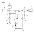
- FIG. 1 is a diagram schematically showing the overall structure of an example of a measuring apparatus used in the measuring method of the present invention.
- This measuring apparatus uses an electromagnetic wave (for example, terahertz wave having a frequency of 20 GHz to 120 THz) generated by irradiating a semiconductor material with laser light irradiated from a laser 2 (for example, a short light pulse laser). It is.
- an electromagnetic wave for example, terahertz wave having a frequency of 20 GHz to 120 THz
- a laser 2 for example, a short light pulse laser
- the laser beam emitted from the laser 2 is branched into two paths by the half mirror 20.
- One is irradiated to the photoconductive element 71 on the electromagnetic wave generation side, and the other is the light on the reception side through the time delay stage 26 by using a plurality of mirrors 21 (numbering is omitted for the same function).
- the conductive element 72 is irradiated.
- the photoconductive elements 71 and 72 a general element in which a dipole antenna having a gap portion is formed in LT-GaAs (low temperature growth GaAs) can be used.
- the laser 2 a fiber type laser or a laser using a solid such as titanium sapphire can be used.
- the semiconductor surface may be used without an antenna, or an electro-optic crystal such as a ZnTe crystal may be used.
- an appropriate bias voltage is applied by the power source 3 to the gap portion of the photoconductive element 71 on the generation side.
- the generated electromagnetic wave is converted into a parallel beam by the parabolic mirror 22 and irradiated to the gap arrangement structure 1 by the parabolic mirror 23.
- the terahertz wave transmitted through the gap arrangement structure 1 is received by the photoconductive element 72 by the parabolic mirrors 24 and 25.
- the electromagnetic wave signal received by the photoconductive element 72 is amplified by the amplifier 6 and then acquired as a time waveform by the lock-in amplifier 4. Then, after a signal processing such as Fourier transform is performed by a PC (personal computer) 5 including a calculating means, the transmittance spectrum of the gap arrangement structure 1 is calculated.
- the bias voltage from the power source 3 applied to the gap of the photoconductive element 71 on the generation side is modulated (amplitude 5V to 30V) by the signal of the oscillator 8.
- the S / N ratio can be improved by performing synchronous detection.
- the measurement method described above is a method generally called terahertz time domain spectroscopy (THz-TDS).
- FIG. 1 shows a case where scattering is transmission, that is, a case where the transmittance of electromagnetic waves is measured.
- scattering means a broad concept including transmission that is a form of forward scattering, reflection that is a form of backscattering, and preferably transmission and reflection. More preferably, transmission in the 0th order direction or reflection in the 0th order direction.
- the grating interval of the diffraction grating is s
- the incident angle is i
- the diffraction angle is ⁇
- the wavelength is ⁇
- the electromagnetic wave used in the present invention is not particularly limited as long as it can cause scattering according to the structure of the void-arranged structure, and any of radio waves, infrared rays, visible rays, ultraviolet rays, X-rays, gamma rays, etc.
- its frequency is not particularly limited, it is preferably 1 GHz to 1 PHz, and more preferably a terahertz wave having a frequency of 20 GHz to 200 THz.
- a linearly polarized electromagnetic wave (linearly polarized wave) having a predetermined polarization direction or an unpolarized electromagnetic wave (nonpolarized wave) can be used.
- linearly polarized electromagnetic waves for example, a terahertz wave generated by the optical rectification effect of an electro-optic crystal such as ZnTe using a short light pulse laser as a light source, visible light emitted from a semiconductor laser, or emitted from a photoconductive antenna An electromagnetic wave etc. are mentioned.
- Non-polarized electromagnetic waves include infrared light emitted from a high-pressure mercury lamp or a ceramic lamp.
- measuring the presence or amount of the object to be measured means quantifying the compound serving as the object to be measured. For example, when measuring the content of a very small amount of the object to be measured such as in a solution, For example, the measurement object is identified.
- gap arrangement structure body used by this invention has the several space
- the plurality of gaps are periodically arranged in at least one direction on the main surface of the gap arrangement structure.
- all of the gaps may be periodically arranged, and within a range that does not impair the effects of the present invention, some of the gaps are periodically arranged and other gaps are non-periodically. It may be arranged.
- the void arrangement structure is preferably a quasi-periodic structure or a periodic structure.
- a quasi-periodic structure is a structure that does not have translational symmetry but is maintained in order. Examples of the quasi-periodic structure include a Fibonacci structure as a one-dimensional quasi-periodic structure and a Penrose structure as a two-dimensional quasi-periodic structure.
- a periodic structure is a structure having spatial symmetry as represented by translational symmetry, and a one-dimensional periodic structure, a two-dimensional periodic structure, or a three-dimensional periodic structure according to the symmetry dimension. Classified into the body. Examples of the one-dimensional periodic structure include a wire grid structure and a one-dimensional diffraction grating. Examples of the two-dimensional periodic structure include a mesh filter and a two-dimensional diffraction grating. Among these periodic structures, a two-dimensional periodic structure is preferably used.
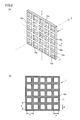
- a plate-like structure in which voids are arranged at regular intervals in a matrix shape as shown in FIG. 2A has two arrangement directions (vertical direction and horizontal direction in the drawing) in which the square gap portions 11 are parallel to each side of the square when viewed from the main surface 10a side.
- the hole size of the gap shown by d in FIG. It is preferable that it is 1/10 or more and 10 times or less of the wavelength. By doing so, the intensity of the scattered electromagnetic wave becomes stronger and the signal can be detected more easily.
- the specific pore size is preferably 0.15 to 150 ⁇ m, and from the viewpoint of improving measurement sensitivity, the pore size is more preferably 0.9 to 9 ⁇ m.
- the lattice spacing (pitch) of the gaps indicated by s in FIG. 2B is measured. It is preferable that it is 1/10 or more and 10 times or less of the wavelength of the electromagnetic wave used for. By doing so, scattering is more likely to occur.
- the specific lattice spacing is preferably 0.15 to 150 ⁇ m, and from the viewpoint of improving measurement sensitivity, the lattice spacing is more preferably 1.3 to 13 ⁇ m.
- the thickness of the void arrangement structure is preferably 5 times or less the wavelength of the electromagnetic wave used for measurement.
- the overall size of the gap arrangement structure is not particularly limited, and is determined according to the area of the beam spot of the irradiated electromagnetic wave.
- the void-arranged structure has a portion that adsorbs to carrier particles described later on the surface thereof.
- the carrier particles are adsorbed on this portion, at least a part of the object to be measured is held in the void arrangement structure via the carrier particles.
- the “part adsorbed on the carrier particles” is not particularly limited as long as it has an adsorptivity to the carrier particles, but preferably has a specific adsorptivity to the carrier particles. “Parts adsorbed on the carrier particles” include a part of the surface of the void-arranged structure made of a material that non-specifically adsorbs to the object to be measured. From the viewpoint of obtaining high measurement sensitivity The portion to be measured is preferably a portion modified with a host molecule described later.
- the present invention it is not necessary to perform all the adsorption of the object to be measured to the void arrangement structure via the carrier particles, and a part of the object to be measured is not contained in the void arrangement structure without the carrier particles. It may be adsorbed directly on the surface.
- the amount of adsorption of the object to be measured on the void arrangement structure increases, and the measurement sensitivity is increased. This is because there are cases where improvement can be considered.
- At least a part of the surface of the void arrangement structure is formed of a conductor.
- the at least part of the surface of the void arrangement structure 1 is any one of the main surface 10a, the side surface 10b, and the void portion side surface 11a shown in FIG.
- the conductor is an object (material) that conducts electricity, and includes not only metals but also semiconductors.
- the metal a metal that can be bonded to a functional group of a compound having a functional group such as a hydroxy group, a thiol group, or a carboxyl group, a metal that can coat a functional group such as a hydroxy group or an amino group on the surface, and these An alloy of these metals can be mentioned.
- Specific examples include gold, silver, copper, iron, nickel, chromium, silicon, germanium, and the like, preferably gold, silver, copper, nickel, and chromium, and more preferably gold and nickel.
- the thiol group can be used to bond the host molecule to the surface of the void structure.
- the host molecule can be bonded to the surface of the void-arranged structure using the alkoxysilane group.
- semiconductors include group IV semiconductors (Si, Ge, etc.), group II-VI semiconductors (ZnSe, CdS, ZnO, etc.), group III-V semiconductors (GaAs, InP, GaN, etc.), group IV compounds, and the like.
- Compound semiconductors such as semiconductors (SiC, SiGe, etc.), I-III-VI semiconductors (CuInSe 2 etc.), and organic semiconductors can be mentioned.
- Carrier particles The measurement method of the present invention is characterized in that at least a part of the object to be measured is held in the void-arranged structure via the carrier particles.
- Carrier particles are particulate substances that can carry an object to be measured.
- the shape of the carrier particles is not particularly limited.
- the size of the carrier particles is preferably smaller than the size of the voids.
- the size of the void portion is the longest distance between two points on the contour in the shape viewed from the main surface direction of the void arrangement structure.
- the void arrangement structure has a square void portion as shown in FIG.
- the pore size of the void portion (d in FIG. 2).
- the size of the carrier particle is the longest distance between two points on the surface of the carrier particle, for example, the diameter of the carrier particle when the carrier particle is substantially spherical. This is because, when the size of the carrier particles is larger than the size of the voids, the voids are blocked with the carrier particles, the desired resonance characteristics of the void-arranged structure cannot be obtained, and measurement becomes difficult.
- the size of the carrier particles is more preferably in the range of 1/200 to 1/2 of the size of the void.
- the average particle diameter of the carrier particles is preferably in the range of 1/200 to 1/2 of the average size of the voids, and preferably 20 nm to 4 ⁇ m.
- the average particle diameter is an average value of primary particle diameters of carrier particles obtained by SEM observation.
- the material of the carrier particles is not particularly limited, and examples thereof include resin materials and metal materials.
- the resin material include (meth) acrylic resins such as polyglycidyl methacrylate, polystyrene resins, and the like.
- examples of the ceramic material include silica and alumina.
- examples of the metal material include gold and silver. A material having a large dielectric constant (or refractive index) is preferable.
- the carrier particles have “parts adsorbing to the object to be measured” and “parts adsorbing to the void-arranged structure” on the surface.
- the “part that adsorbs to the object to be measured” includes a part composed of a material that adsorbs nonspecifically to the object to be measured.
- the host molecule for the object to be measured It is preferably a moiety modified with
- a portion adsorbing to the void arrangement structure includes a portion made of a material that non-specifically adsorbs to the void arrangement structure. From the viewpoint of obtaining high measurement sensitivity, the void arrangement structure It is preferably a moiety modified with a host molecule.
- adsorption includes, for example, physical adsorption by intermolecular force (van der Waals force) and chemical adsorption by chemical bond.
- chemical bonds include covalent bonds (for example, covalent bonds between metal and thiol groups), ionic bonds, metal bonds, hydrogen bonds, and the like.
- the host molecule is a molecule that specifically adsorbs to the object to be measured.
- examples of combinations of host molecules and analytes include antigen and antibody, sugar chain and protein, lipid and protein, low molecular weight compound (ligand) and protein, protein and protein, single-stranded DNA and single-stranded DNA, etc. Can be mentioned.
- Specific examples of the host molecule include molecules having a biotin group, a carboxyl group, a sulfo group, an amino group, and the like, and proteins such as streptavidin, proteins A and G, and antibodies.
- the object to be measured is adsorbed on the carrier particles, and then the carrier particles are adsorbed on the void arrangement structure, thereby holding the object to be measured on the void arrangement structure via the carrier particles.
- the solution of the carrier particles as described above is mixed with the solution of the object to be measured, and the object to be measured is adsorbed on the carrier particles.
- the void arrangement structure is immersed in the mixed solution, and at least a part of the measurement object is adsorbed on the surface of the void arrangement structure via the carrier particles.
- the void-arranged structure is taken out from the mixed solution, the solvent, excess carrier particles, and the object to be measured are washed, and the void-arranged structure is dried, and then the object to be measured is measured using the measuring device as described above. Measure the characteristics.
- various known methods can be employed as a method for adsorbing the object to be measured on the carrier particles and a method for adsorbing the carrier particles on the void-arranged structure.
- the measurement object is held in the gap arrangement structure together with the carrier particles, thereby obtaining a label effect by the carrier particles. . That is, when the amount of the substance adsorbed on the void-arranged structure is larger than that of the actual object to be measured, the amount of change in the characteristics of the scattered electromagnetic wave is increased and the measurement sensitivity is improved.
- the contaminants contained in the solution of the object to be measured are reduced by the process of adsorbing the object to be measured to the carrier particles, nonspecific adsorption of the contaminants to the void arrangement structure, etc. Is reduced and measurement sensitivity is improved.
- the presence / absence or amount of the object to be measured is measured based on at least one parameter relating to the characteristics of the electromagnetic wave scattered in the void-arranged structure obtained as described above.
- the dip waveform generated in the frequency characteristic of the electromagnetic wave forward scattered (transmitted) in the void-arranged structure 1 and the peak waveform generated in the frequency characteristic of the electromagnetic wave back scattered (reflected) vary depending on the presence of the object to be measured.
- the presence or amount of the object to be measured can be measured based on the measurement.
- the dip waveform refers to the frequency characteristic (for example, transmittance spectrum) of the void-arranged structure in a frequency range in which the ratio of the detected electromagnetic wave to the irradiated electromagnetic wave (for example, the transmittance of the electromagnetic wave) is relatively large. It is the waveform of the part of the valley type (convex downward) seen partially.
- the peak waveform is a part of the frequency characteristics (for example, reflectance spectrum) of the void-arranged structure in a frequency range where the ratio of the detected electromagnetic wave to the irradiated electromagnetic wave (for example, the reflectance of the electromagnetic wave) is relatively small. It is a mountain-shaped (convex upward) waveform.
- Embodiment 2 This embodiment is carried out in that the carrier particles are adsorbed on the void arrangement structure, and then the measurement object is adsorbed on the carrier particles, thereby holding the measurement object on the void arrangement structure via the carrier particles. Different from Form 1. Since other points are the same as those of the first embodiment, description thereof is omitted.
- the void portion of the void arrangement structure is miniaturized (for example, the size of the void portion is several ⁇ m or less), a finer porosity (for example, so as not to affect the resonance characteristics of the entire void arrangement structure) It is technically difficult to apply plating having nano-level porosity.
- the particle size of the carrier particles is relatively easy to miniaturize.
- the size of the porous layer formed by the adsorption of the carrier particles can be controlled to the nano level.
- the measuring method and measuring device which were excellent in measurement sensitivity compared with the past are provided.
- the pore diameter of the obtained porous layer can be uniformly controlled, and a measurement method and a measurement device excellent in reproducibility of resonance characteristics are provided. .
- Example 1 In this example, as shown in FIG. 2, a structure in which square voids are periodically arranged in a square lattice pattern in the main surface direction of a flat plate structure (void arrangement structure) and carrier particles are provided. Used to measure cholera toxin in biological samples.
- the void arrangement structure used in this example was manufactured by the following method.
- a stainless steel conductive plate having a 300 mm square smooth surface is prepared, and a photosensitive thick film photoresist (manufactured by JSR) is applied to a thickness of 5 ⁇ m on one main surface thereof, and the photosensitive resin material is dried. Thus, a photosensitive resin layer was formed.
- the portion corresponding to the gaps 11 of the photosensitive thick film photoresist was UV cured.
- the uncured portion of the photosensitive thick film photoresist corresponding to the portion other than the void portion 11 (structure portion) was removed with a rinsing liquid to expose the stainless steel conductor plate.
- the peeling polymer solution was apply
- the conductor plate thus prepared was placed in a Ni electrolytic plating bath and energized to form a Ni plating film with a thickness of 1.5 ⁇ m only on the release layer formed on the exposed portion of the conductor plate. Thereafter, the cured portion of the photosensitive resin layer remaining on the conductor plate was removed with a solvent, and the Ni plating film was peeled from the conductor plate. The surface of the obtained Ni plating film was subjected to electroless Au plating to obtain a Ni gap arrangement structure A covered with Au.
- void portions having a pore size of 4 ⁇ m were arranged at a pitch of 6.5 ⁇ m, and the thickness was 1.5 ⁇ m.
- the shape of the void arrangement structure viewed from the main surface direction was a circle with a diameter of 6 mm.
- nano-particles having a high dispersibility of about 200 nm in diameter with polyglycidyl methacrylate as the main component were used.
- the surface of the nanoparticle is modified with a carboxyl group, and any compound having an amino group can be supported via the carboxyl group.
- FG beads COOH beads
- ganglioside GM1 which is a receptor for cholera toxin (object to be measured) was immobilized on the surface of the nanoparticle. Immobilization was performed by forming an amino bond between the carboxy group on the surface of the carrier particle and the amino group of the ganglioside GM1 lyso form, which is a receptor for cholera toxin.
- carrier particles hereinafter, sometimes referred to as GM1 immobilized particles
- nano-particles having a high dispersibility of about 200 nm in diameter and having polyglycidyl methacrylate as a main component, to which ganglioside GM1 is immobilized, are prepared. did.
- the void-arranged structure A was immersed in acetone, washed with shaking for 10 minutes, taken out into another beaker, and dried with nitrogen gas.
- the void-arranged structure A was immersed for 20 hours at room temperature in a 5 mL sample tube bottle in which 250 ⁇ L of the cation adsorption type self-assembled film forming reagent was charged. Thereafter, the void-arranged structure A was taken out, washed with ethanol, dried with nitrogen gas, and held with a fixing jig.
- the void-arranged structure A was immersed in acetone, washed with shaking for 10 minutes, taken out into another beaker, and dried with nitrogen gas. Next, the void-arranged structure A was immersed for 20 hours at room temperature in a 5 mL sample tube bottle into which 250 mL of an anion adsorption type self-assembled film-forming reagent had been charged. Thereafter, the void-arranged structure A was taken out, washed with ethanol, dried with nitrogen gas, and held with a fixing jig.
- GM1 immobilized particles 100 ⁇ g of GM1 immobilized particles are collected in a tube, and 200 ⁇ L of buffer A (0.05 M Tris, 0.2 M NaCl, 0.001 M Na 2 EDTA, pH 7.5) is added, and the GM1 immobilized particles are added to the buffer. Dispersed. Thereafter, GM1 immobilized particles were settled using a neodymium magnet, and the supernatant was discarded (this operation is hereinafter referred to as magnetic separation). This was repeated twice, and the GM1 immobilized particles were washed with buffer A three times in total.
- buffer A 0.05 M Tris, 0.2 M NaCl, 0.001 M Na 2 EDTA, pH 7.5
- a cholera toxin solution (List Biological Laboratories) using 20 ⁇ g / mL of buffer A as a solvent is prepared, and GM1 immobilized particles are dispersed in 400 ⁇ L of the cholera toxin solution.
- the binding reaction was performed over time. Thereafter, magnetic separation was performed, and the supernatant was discarded.
- GM1 immobilized particles were dispersed in 200 ⁇ L of Buffer A, magnetic separation was performed, and the supernatant was discarded. This was repeated twice, and the GM1 immobilized particles were washed with buffer A three times in total. After washing, GM1 immobilized particles were dispersed in 200 ⁇ L of buffer A and kept at 4 ° C.
- the void arrangement structure A subjected to the above two types of surface treatment, and the void structure A not subjected to the surface treatment are placed on the surface at 30 at room temperature. Left to stand. Thereafter, 4 mL of buffer solution A was added, shaken for 5 minutes, and then the operation of discarding buffer solution A was performed twice, thereby washing void-arranged structure A with buffer solution A. Then, after adding 4 mL of water and shaking for 5 minutes, the operation of discarding water was performed twice, and the void-arranged structure A was washed twice with water. Thereafter, the void-arranged structure A was dried under reduced pressure for 10 minutes.
- the transmission spectrum of the void-arranged structure adsorbed with cholera toxin and GM1 immobilized particles thus obtained was measured by FT-IR.
- the electromagnetic waves were irradiated from a direction perpendicular to the main surface of the void-arranged structure.
- the void-arranged structure A was washed with the buffer A by carrying out the operation of discarding the buffer A twice after adding 4 mL of the buffer A to the void-arranged structure A and shaking for 5 minutes. Then, after adding 4 mL of water and shaking for 5 minutes, the operation of discarding water was performed twice, and the void-arranged structure A was washed twice with water. Thereafter, the void-arranged structure A was dried under reduced pressure for 10 minutes.
- the transmission spectrum was measured by FT-IR.
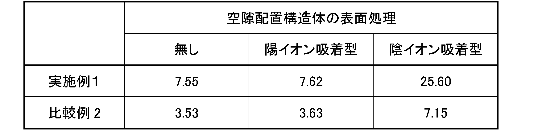
- Table 1 shows the wave number (cm ⁇ 1 ) at which the transmittance is maximum in the transmission spectra obtained by the measurement in Example 1, Comparative Example 1, and Comparative Example 2.
- Shift wavenumber transmittance of Example 1 is maximized, if not performed a self-assembled film forming process 7.55Cm -1, if you make a cation adsorption treatment 7.62 cm -1, Yin When ion adsorption treatment was performed, it was 25.6 cm ⁇ 1 .
- the wave number of the transmittance of Comparative Example 2 is maximum, if you did not self-assembled film forming process 3.53Cm -1, if you make a cation adsorption treatment 3.63Cm -1, anionic When the adsorption treatment was performed, it was 7.15 cm ⁇ 1 .
- Example 1 using carrier particles has a larger wave number shift amount at which the transmittance is maximum, and the measurement sensitivity is significantly improved. confirmed.
- Example 2 A void arrangement structure B similar to that of Example 1 was prepared except that the surface was not subjected to electroless Au plating.
- a biotin molecule having an alkoxysilane terminal and ethanol were prepared, and a biotin solution having a concentration of 500 ⁇ g / mL was prepared.
- the void-arranged structure B was immersed in a biotin solution for about 12 hours, and after immersion, washed with ultrapure water to obtain a void-arranged structure B having biotin molecules immobilized on the surface.
- a streptavidin solution having a concentration of 500 ⁇ g / mL was prepared using a PBS solution.
- biotin-immobilized SiO 2 nanoparticles were added to the above streptavidin solution, dispersed, and allowed to stand at room temperature for about 12 hours. And it wash
- streptavidin-immobilized SiO 2 nanoparticles were added to the PBS solution and dispersed, and then the biotin molecule-immobilized void arrangement structure B was immersed and left for 12 hours. After leaving, the void-arranged structure B was washed with water, and further immersed and left in a PBS solution of streptavidin having a concentration of 500 [ ⁇ g / mL] for 12 hours. After the void-arranged structure B was washed with water and dried, the transmission characteristics were evaluated using FT-IR as the initial characteristics.
- a DNA single strand (17mer, sequence GTA AAA CGA CGG CCA GT) labeled with biotin at the 5 ′ end side was prepared as an object to be measured.
- the void arrangement structure B for which the initial characteristic evaluation was completed was immersed in a PBS solution of biotin-labeled DNA having a concentration of 500 [ ⁇ g / mL] and left for 12 hours. After leaving, the void-arranged structure B is washed with water and dried so that the biotin-labeled DNA single strand to be measured is streptavidin-immobilized SiO 2 nanoparticle surface or the void-arranged structure. A sample adsorbed on the surface was obtained. The transmission characteristics were evaluated using FT-IR, and the change from the initial characteristics was evaluated.
- the void-arranged structure B whose initial characteristics were evaluated was immersed in a PBS solution of biotin-labeled DNA having a concentration of 500 [ ⁇ g / mL] and allowed to stand for 12 hours. After leaving, the void-arranged structure B was washed with water and dried to obtain a sample in which the single-stranded biotin-labeled DNA as the measurement object was adsorbed on the surface of the void-arranged structure via streptavidin. The transmission characteristics of the sample were evaluated using FT-IR, and the change from the initial characteristics was determined.
- FIG. 4 shows a graph comparing the initial value and the post-measurement object adsorption with respect to the transmittance peak frequency [THz] from the results of Example 2 and Comparative Example 3. From the results shown in FIG. 4, in Example 2, the amount of change in the transmission peak frequency after adsorption of the object to be measured is larger than that in Comparative Example 3, and the measurement sensitivity is improved. You can see that
- 1 void arrangement structure 10a main surface, 10b side surface, 10c outer periphery, 101 protrusion, 11 void portion, 11a void side surface, 2 laser, 20 half mirror, 21 mirror, 22, 23, 24, 25 parabolic mirror , 26 time delay stage, 3 power supply, 4 lock-in amplifier, 5 PC (personal computer), 6 amplifier, 71, 72 photoelectric conducting element, 8 oscillator.
- PC personal computer
Landscapes
- Physics & Mathematics (AREA)
- General Physics & Mathematics (AREA)
- Immunology (AREA)
- Pathology (AREA)
- Analytical Chemistry (AREA)
- Biochemistry (AREA)
- General Health & Medical Sciences (AREA)
- Life Sciences & Earth Sciences (AREA)
- Health & Medical Sciences (AREA)
- Chemical & Material Sciences (AREA)
- Electromagnetism (AREA)
- Engineering & Computer Science (AREA)
- Computer Networks & Wireless Communication (AREA)
- Radar, Positioning & Navigation (AREA)
- Remote Sensing (AREA)
- Investigating Or Analysing Materials By Optical Means (AREA)
Description
本発明は、被測定物の測定方法およびそれに用いる測定デバイスに関する。より詳しくは、空隙部を有する空隙配置構造体に被測定物を保持し、該空隙配置構造体に電磁波を照射して、空隙配置構造体で散乱した電磁波の特性を検出することにより、被測定物の有無または量を測定する測定方法、および、それに用いる測定デバイスに関する。
従来から、物質の特性を分析するために、空隙配置構造体に被測定物を保持して、その被測定物が保持された空隙配置構造体に電磁波を照射し、その透過スペクトル等を解析して被測定物の有無または量を検出する測定方法が用いられている。具体的には、例えば、金属メッシュフィルタに付着したタンパク質などの被測定物に、テラヘルツ波を照射して透過スペクトルを解析する手法が挙げられる。
このような電磁波を用いた透過スペクトルの解析手法の従来技術として、特許文献1には、被測定物が保持された空隙領域を有する空隙配置構造体(具体的には、メッシュ状の導体板)に向かって、空隙配置構造体の主面に垂直な方向に対して斜めの方向から電磁波を照射して、空隙配置構造体を透過した電磁波を測定し、測定値の周波数特性に生じたディップ波形の位置が、被測定物の存在により移動することに基づいて被測定物の特性を検出する測定方法が開示されている。
しかしながら、このような従来技術よりも、さらに測定感度に優れた測定方法の提供が望まれていた。
本発明は、従来よりも、さらに測定感度に優れた測定方法、および、それに用いられる測定デバイスを提供することを目的とする。
本発明は、被測定物が保持された空隙配置構造体に電磁波を照射して、前記空隙配置構造体で散乱された電磁波の特性を検出することにより、前記被測定物の有無または量を測定する方法であって、
前記空隙配置構造体は、その主面に垂直な方向に貫通した複数の空隙部を有し、
前記被測定物の少なくとも一部は担体粒子を介して前記空隙配置構造体に保持されることを特徴とする、測定方法である。
前記空隙配置構造体は、その主面に垂直な方向に貫通した複数の空隙部を有し、
前記被測定物の少なくとも一部は担体粒子を介して前記空隙配置構造体に保持されることを特徴とする、測定方法である。
前記担体粒子は前記空隙部より小さいことが好ましい。
前記被測定物を前記担体粒子に吸着させ、その後に前記担体粒子を前記空隙配置構造体に吸着させることにより、前記被測定物の少なくとも一部が担体粒子を介して前記空隙配置構造体に保持されることが好ましい。
前記被測定物を前記担体粒子に吸着させ、その後に前記担体粒子を前記空隙配置構造体に吸着させることにより、前記被測定物の少なくとも一部が担体粒子を介して前記空隙配置構造体に保持されることが好ましい。
前記担体粒子を前記空隙配置構造体に吸着させ、その後に前記被測定物を前記担体粒子に吸着させることにより、前記被測定物の少なくとも一部が担体粒子を介して前記空隙配置構造体に保持されることが好ましい。
前記担体粒子は、その表面に、前記被測定物に吸着する部分および前記空隙配置構造体に吸着する部分を有していることが好ましい。
前記空隙配置構造体は、その表面に、前記担体粒子に吸着する部分を有していることが好ましい。
前記担体粒子において、前記被測定物と吸着する部分は、前記被測定物に特異的に吸着するホスト分子で修飾されていることが好ましい。
また、本発明は、上記の測定方法に用いられる測定デバイスであって、
空隙配置構造体、および、該空隙配置構造体に保持された担体粒子を含み、
前記空隙配置構造体は、その主面に垂直な方向に貫通した複数の空隙部を有し、
前記担体粒子は、その表面に前記被測定物と吸着する部分を有している、測定デバイスにも関する。
空隙配置構造体、および、該空隙配置構造体に保持された担体粒子を含み、
前記空隙配置構造体は、その主面に垂直な方向に貫通した複数の空隙部を有し、
前記担体粒子は、その表面に前記被測定物と吸着する部分を有している、測定デバイスにも関する。
本発明によれば、従来よりも、さらに測定感度に優れた測定方法、および、それに用いられる測定デバイスを提供することができる。
まず、本発明の測定方法の一例の概略を図1を用いて説明する。図1は、本発明の測定方法に用いられる測定装置の一例の全体構造を模式的に示す図である。この測定装置は、レーザ2(例えば、短光パルスレーザ)から照射されるレーザ光を半導体材料に照射することで発生する電磁波(例えば、20GHz~120THzの周波数を有するテラヘルツ波)パルスを利用するものである。
図1の構成において、レーザ2から出射したレーザ光を、ハーフミラー20で2つの経路に分岐する。一方は、電磁波発生側の光伝導素子71に照射され、もう一方は、複数のミラー21(同様の機能のものは付番を省略)を用いることで、時間遅延ステージ26を経て受信側の光伝導素子72に照射される。光伝導素子71、72としては、LT-GaAs(低温成長GaAs)にギャップ部をもつダイポールアンテナを形成した一般的なものを用いることができる。また、レーザ2としては、ファイバー型レーザやチタンサファイアなどの固体を用いたレーザなどを使用できる。さらに、電磁波の発生、検出には、半導体表面をアンテナなしで用いたり、ZnTe結晶の様な電気光学結晶を用いたりしてもよい。ここで、発生側となる光伝導素子71のギャップ部には、電源3により適切なバイアス電圧が印加されている。
発生した電磁波は放物面ミラー22で平行ビームにされ、放物面ミラー23によって、空隙配置構造体1に照射される。空隙配置構造体1を透過したテラヘルツ波は、放物面ミラー24,25によって光伝導素子72で受信される。光伝導素子72で受信された電磁波信号は、アンプ6で増幅されたのちロックインアンプ4で時間波形として取得される。そして、算出手段を含むPC(パーソナルコンピュータ)5でフーリエ変換などの信号処理された後に、空隙配置構造体1の透過率スペクトルなどが算出される。ロックインアンプ4で取得するために、発振器8の信号で発生側の光伝導素子71のギャップに印加する電源3からのバイアス電圧を変調(振幅5V~30V)している。これにより同期検波を行うことでS/N比を向上させることができる。
以上に説明した測定方法は、一般にテラヘルツ時間領域分光法(THz-TDS)と呼ばれる方法である。
図1では、散乱が透過である場合、すなわち電磁波の透過率を測定する場合を示している。本発明において「散乱」とは、前方散乱の一形態である透過や、後方散乱の一形態である反射などを含む広義の概念を意味し、好ましくは透過や反射である。さらに好ましくは、0次方向の透過や0次方向の反射である。
なお、一般的に、回折格子の格子間隔をs、入射角をi、回折角をθ、波長をλとしたとき、回折格子によって回折されたスペクトルは、
s(sin i -sin θ)=nλ …(1)
と表すことができる。上記「0次方向」の0次とは、上記式(1)のnが0の場合を指す。sおよびλは0となり得ないため、n=0が成立するのは、sin i- sin θ=0の場合のみである。従って、上記「0次方向」とは、入射角と回折角が等しいとき、つまり電磁波の進行方向が変わらないような方向を意味する。
s(sin i -sin θ)=nλ …(1)
と表すことができる。上記「0次方向」の0次とは、上記式(1)のnが0の場合を指す。sおよびλは0となり得ないため、n=0が成立するのは、sin i- sin θ=0の場合のみである。従って、上記「0次方向」とは、入射角と回折角が等しいとき、つまり電磁波の進行方向が変わらないような方向を意味する。
本発明で用いられる電磁波は、空隙配置構造体の構造に応じて散乱を生じさせることのできる電磁波であれば特に限定されず、電波、赤外線、可視光線、紫外線、X線、ガンマ線等のいずれも使用することができ、その周波数も特に限定されるものではないが、好ましくは1GHz~1PHzであり、さらに好ましくは20GHz~200THzの周波数を有するテラヘルツ波である。
電磁波は、例えば、所定の偏波方向を有する直線偏光の電磁波(直線偏波)や無偏光の電磁波(無偏波)を用いることができる。直線偏光の電磁波としては、例えば、短光パルスレーザを光源としてZnTe等の電気光学結晶の光整流効果により発生するテラヘルツ波や、半導体レーザから出射される可視光や、光伝導アンテナから放射される電磁波等が挙げられる。無偏光の電磁波としては、高圧水銀ランプやセラミックランプから放射される赤外光等が挙げられる。
本発明において、被測定物の有無または量を測定するとは、被測定物となる化合物の定量を行うことであり、例えば、溶液中等の微量の被測定物の含有量を測定する場合や、被測定物の同定を行う場合などが挙げられる。
(空隙配置構造体)
本発明で用いられる空隙配置構造体は、その主面に垂直な方向に貫通した複数の空隙部を有している。例えば、複数の該空隙部は、空隙配置構造体の主面上の少なくとも一方向に周期的に配置されている。ただし、空隙部は、その全てが周期的に配置されていてもよく、本発明の効果を損なわない範囲で、一部の空隙部が周期的に配置され、他の空隙部が非周期的に配置されていてもよい。
本発明で用いられる空隙配置構造体は、その主面に垂直な方向に貫通した複数の空隙部を有している。例えば、複数の該空隙部は、空隙配置構造体の主面上の少なくとも一方向に周期的に配置されている。ただし、空隙部は、その全てが周期的に配置されていてもよく、本発明の効果を損なわない範囲で、一部の空隙部が周期的に配置され、他の空隙部が非周期的に配置されていてもよい。
空隙配置構造体は、好ましくは準周期構造体や周期構造体である。準周期構造体とは、並進対称性は持たないが配列には秩序性が保たれている構造体のことである。準周期構造体としては、例えば、1次元準周期構造体としてフィボナッチ構造、2次元準周期構造体としてペンローズ構造が挙げられる。周期構造体とは、並進対称性に代表される様な空間対称性を持つ構造体のことであり、その対称の次元に応じて1次元周期構造体、2次元周期構造体、3次元周期構造体に分類される。1次元周期構造体は、例えば、ワイヤーグリッド構造、1次元回折格子などが挙げられる。2次元周期構造体は、例えば、メッシュフィルタ、2次元回折格子などが挙げられる。これらの周期構造体のうちでも、2次元周期構造体が好適に用いられる。
2次元周期構造体としては、例えば、図2に示すようなマトリックス状に一定の間隔で空隙部が配置された板状構造体(格子状構造体)が挙げられる。図2(a)に示す空隙配置構造体1は、その主面10a側からみて正方形の空隙部11が、該正方形の各辺と平行な2つの配列方向(図中の縦方向と横方向)に等しい間隔で設けられた板状構造体である。
空隙配置構造体の空隙部の寸法や配置、空隙配置構造体の厚み等は、特に制限されず、測定方法や、空隙配置構造体の材質特性、使用する電磁波の周波数等に応じて適宜設計される。
例えば、空隙部が図2(a)に示すように縦横に規則的に配置された空隙配置構造体1において、図2(b)にdで示される空隙部の孔サイズは、測定に用いる電磁波の波長の10分の1以上、10倍以下であることが好ましい。このようにすることで、散乱する電磁波の強度がより強くなり、信号をより検出しやすくなる。具体的な孔サイズは0.15~150μmであることが好ましく、測定感度向上の観点からは、孔サイズが0.9~9μmであることがより好ましい。
また、空隙部が図2(a)に示すように縦横に規則的に配置された空隙配置構造体1において、図2(b)にsで示される空隙部の格子間隔(ピッチ)は、測定に用いる電磁波の波長の10分の1以上、10倍以下であることが好ましい。このようにすることで、散乱がより生じやすくなる。具体的な格子間隔は0.15~150μmであることが好ましく、測定感度向上の観点からは、格子間隔が1.3~13μmであることがより好ましい。
また、空隙配置構造体の厚みは、測定に用いる電磁波の波長の5倍以下であることが好ましい。このようにすることで、散乱する電磁波の強度がより強くなって信号を検出しやすくなる。
空隙配置構造体の全体の寸法は、特に制限されず、照射される電磁波のビームスポットの面積等に応じて決定される。
空隙配置構造体は、その表面に、後述の担体粒子に吸着する部分を有していることが好ましい。この部分に担体粒子が吸着することにより、被測定物の少なくとも一部は、担体粒子を介して前記空隙配置構造体に保持される。
「担体粒子に吸着する部分」は、担体粒子に対する吸着性を有していれば特に限定されないが、担体粒子に対する特異的な吸着性を有していることが好ましい。「担体粒子に吸着する部分」には、被測定物に非特異的に吸着するような材質から構成される空隙配置構造体の表面の一部も含まれるが、高い測定感度を得る観点からは、被測定物に対する後述のホスト分子で修飾された部分であることが好ましい。
ただし、本発明においては、被測定物の空隙配置構造体への吸着の全てを担体粒子を介して行う必要はなく、被測定物の一部を、担体粒子を介さずに空隙配置構造体の表面に直接吸着してもよい。空隙配置構造体への担体粒子を介した吸着と、空隙配置構造体への直接的な吸着とを併用することにより、空隙配置構造体への被測定物の吸着量が増加し、測定感度を向上できる場合も考えられるからである。
空隙配置構造体は、少なくとも一部の表面が導体で形成されていることが好ましい。空隙配置構造体1の少なくとも一部の表面とは、図2(a)に示す主面10a、側面10b、空隙部側面11aのうちいずれかの一部の表面である。
ここで、導体とは、電気を通す物体(物質)のことであり、金属だけでなく半導体も含まれる。金属としては、ヒドロキシ基、チオール基、カルボキシル基などの官能基を有する化合物の官能基と結合することのできる金属や、ヒドロキシ基、アミノ基などの官能基を表面にコーティングできる金属、ならびに、これらの金属の合金を挙げることができる。具体的には、金、銀、銅、鉄、ニッケル、クロム、シリコン、ゲルマニウムなどが挙げられ、好ましくは金、銀、銅、ニッケル、クロムであり、さらに好ましくは金、ニッケルである。金、ニッケルを用いた場合、特にホスト分子がチオール基(-SH基)を有する場合に該チオール基を用いてホスト分子を空隙配置構造体の表面に結合させることができるため有利である。また、ニッケルを用いた場合、特にホスト分子がアルコキシシラン基を有する場合、該アルコキシシラン基を用いてホスト分子を空隙配置構造体の表面に結合させることができるため有利である。また、半導体としては、例えば、IV族半導体(Si、Geなど)や、II-VI族半導体(ZnSe、CdS、ZnOなど)、III-V族半導体(GaAs、InP、GaNなど)、IV族化合物半導体(SiC、SiGeなど)、I-III-VI族半導体(CuInSe2など)などの化合物半導体、有機半導体が挙げられる。
(担体粒子)
本発明の測定方法は、被測定物の少なくとも一部が、担体粒子を介して空隙配置構造体に保持されることを特徴とする。「担体粒子」とは、被測定物等を担持することのできる粒子状の物質である。担体粒子の形状は、特に限定されない。
本発明の測定方法は、被測定物の少なくとも一部が、担体粒子を介して空隙配置構造体に保持されることを特徴とする。「担体粒子」とは、被測定物等を担持することのできる粒子状の物質である。担体粒子の形状は、特に限定されない。
担体粒子のサイズは、空隙部のサイズより小さいことが好ましい。空隙部のサイズとは、空隙配置構造体の主面方向から見た形状における輪郭上の2点間の最長の距離であり、例えば、空隙配置構造体が図2に示すような正方形の空隙部を有する構造体である場合、空隙部の孔サイズ(図2のd)である。担体粒子のサイズとは、担体粒子の表面上の2点間の最長の距離であり、例えば、担体粒子が実質的に球状である場合は担体粒子の直径である。担体粒子のサイズが空隙部のサイズより大きい場合、空隙部が担体粒子で塞がれてしまい、空隙配置構造体の所望の共振特性が得られず、測定が困難になるからである。
担体粒子のサイズは、空隙部のサイズの1/200~1/2の範囲内にあることがより好ましい。具体的には、担体粒子の平均粒子径が、空隙部のサイズ平均値の1/200~1/2の範囲内にあることが好ましく、20nm~4μmであることが好ましい。ここで、平均粒子径とは、SEM観察により求めた担体粒子の一次粒子径の平均値である。
担体粒子の材質は、特に限定されないが、例えば、樹脂材料や金属材料が挙げられる。樹脂材料としては、例えば、ポリグリシジルメタクリレートなどの(メタ)アクリル樹脂やポリスチレン樹脂等が挙げられる。また、セラミック材料としては、シリカやアルミナ等が挙げられる。金属材料としては、金、銀などが挙げられる。好ましくは誘電率(あるいは屈折率)が大きな材料である。
担体粒子は、その表面に、「被測定物に吸着する部分」および「空隙配置構造体に吸着する部分」を有していることが好ましい。
「被測定物と吸着する部分」には、被測定物に非特異的に吸着するような材質から構成される部分も含まれるが、高い測定感度を得る観点からは、被測定物に対するホスト分子で修飾された部分であることが好ましい。
「空隙配置構造体に吸着する部分」には、空隙配置構造体に非特異的に吸着するような材質から構成される部分も含まれるが、高い測定感度を得る観点からは、空隙配置構造体に対するホスト分子で修飾された部分であることが好ましい。
なお、本発明において、「吸着」には、例えば、分子間力(ファンデルワールス力)による物理吸着や、化学結合による化学吸着が含まれる。化学結合としては、共有結合(例えば、金属―チオール基間の共有結合など)、イオン結合、金属結合、水素結合などが挙げられる。
ホスト分子とは、被測定物に特異的に吸着する分子である。ホスト分子と被測定物の組み合わせとしては、例えば、抗原と抗体、糖鎖とタンパク質、脂質とタンパク質、低分子化合物(リガンド)とタンパク質、タンパク質とタンパク質、一本鎖DNAと一本鎖DNAなどが挙げられる。ホスト分子の具体例としては、ビオチン基、カルボキシル基、スルホ基、アミノ基等を有する分子や、ストレプトアビジン、プロテインAやG、抗体などのタンパク質が挙げられる。
(実施形態1)
本実施形態では、被測定物を担体粒子に吸着させ、その後に担体粒子を空隙配置構造体に吸着させることにより、被測定物を担体粒子を介して空隙配置構造体に保持する。
本実施形態では、被測定物を担体粒子に吸着させ、その後に担体粒子を空隙配置構造体に吸着させることにより、被測定物を担体粒子を介して空隙配置構造体に保持する。
より具体的には、例えば、被測定物の溶液に上述のような担体粒子の溶液を混合して、被測定物を担体粒子に吸着させる。次に、該混合液中に空隙配置構造体を浸漬し、空隙配置構造体の表面に被測定物の少なくとも一部を担体粒子を介して吸着させる。次に、空隙配置構造体を混合液中から取り出し、溶媒や余分な担体粒子や被測定物を洗浄し、空隙配置構造体を乾燥してから、上述のような測定装置を用いて被測定物の特性を測定する。
本発明において、担体粒子に被測定物を吸着させる方法や、空隙配置構造体に担体粒子を吸着させる方法としては、種々公知の方法を採用することができる。
本実施形態によれば、被測定物のみを空隙配置構造体に吸着させる方法と比べて、被測定物が担体粒子と共に空隙配置構造体に保持されることにより、担体粒子によるラベル効果が得られる。すなわち、空隙配置構造体に吸着する物質量が、実際の被測定物よりも増大することで、散乱電磁波の特性の変化量が増大し、測定感度が向上する。
また、被測定物を担体粒子に吸着させる工程を経ることにより、被測定物の溶液等に含まれる共雑物が低減されるため、空隙配置構造体への共雑物の非特異的吸着等が低減され、測定感度が向上する。
本発明の測定方法においては、上述のようにして求められる空隙配置構造体において散乱した電磁波の特性に関する少なくとも1つのパラメータに基づいて、被測定物の有無または量が測定される。例えば、空隙配置構造体1において前方散乱(透過)した電磁波の周波数特性に生じたディップ波形や、後方散乱(反射)した電磁波の周波数特性に生じたピーク波形などが、被測定物の存在により変化することに基づいて被測定物の有無または量を測定することができる。
ここで、ディップ波形とは、照射した電磁波に対する検出した電磁波の比率(例えば、電磁波の透過率)が相対的に大きくなる周波数範囲において、空隙配置構造体の周波数特性(例えば、透過率スペクトル)に部分的に見られる谷型(下に凸)の部分の波形である。また、ピーク波形とは、照射した電磁波に対する検出した電磁波の比率(例えば、電磁波の反射率)が相対的に小さくなる周波数範囲において、空隙配置構造体の周波数特性(例えば、反射率スペクトル)に部分的に見られる山型(上に凸)の波形である。
(実施形態2)
本実施形態は、担体粒子を空隙配置構造体に吸着させ、その後に被測定物を担体粒子に吸着させることにより、被測定物を担体粒子を介して空隙配置構造体に保持する点において、実施形態1とは異なる。他の点については実施形態1と同様であるため、説明は省略する。
本実施形態は、担体粒子を空隙配置構造体に吸着させ、その後に被測定物を担体粒子に吸着させることにより、被測定物を担体粒子を介して空隙配置構造体に保持する点において、実施形態1とは異なる。他の点については実施形態1と同様であるため、説明は省略する。
測定感度向上のために、空隙配置構造体に保持される被測定物の絶対量を増加させる方法の1つとして、空隙配置構造体の表面積を大きくすることが考えられる。例えば、空隙配置構造体の表面に多孔めっき等を施すことにより、空隙配置構造体の表面積を増加させる方法が挙げられる。
一方で、多くの被測定物に対して、測定感度を向上させるためには、空隙配置構造体の空隙部のサイズおよびピッチを小さくすることが望ましい。これにより、電磁波を照射した際に共振現象が生じている空間を小さくすること、すなわち、局在電磁界領域を小さくすることで、その範囲内における被測定物の有無による散乱電磁波の特性変化への影響が大きくなり、より微小(あるいは微量)な被測定物を測定できるためである。
しかし、空隙配置構造体の空隙部を微小化する場合(例えば、空隙部のサイズが数μm以下)において、空隙配置構造体全体の共振特性に影響を与えないように、さらに微小な多孔(例えば、ナノレベルの多孔)を有するめっきを施すことは技術的に困難である。
これに対して、本実施形態のように、担体粒子を空隙配置構造体の表面に吸着させる場合においては、担体粒子の粒径は微小化が比較的容易であるため、粒径を、例えばナノレベルに制御することで、該担体粒子の吸着によって形成される多孔質層の多孔のサイズをナノレベルに制御することが可能となる。これにより、従来よりも測定感度に優れた測定方法および測定デバイスが提供される。また、担体粒子の粒径分布を均一に制御することにより、得られる多孔質層の孔径も均一に制御することが可能となり、共振特性の再現性に優れた測定方法および測定デバイスが提供される。
以下、実施例を挙げて本発明をより詳細に説明するが、本発明はこれらに限定されるものではない。
(実施例1)
本実施例では、図2に示されるような、正方形状の空隙部が平板状の構造体の主面方向に正方格子状に周期配置された構造体(空隙配置構造体)と担体粒子とを用いて、生体試料中のコレラ毒素の測定を行った。
本実施例では、図2に示されるような、正方形状の空隙部が平板状の構造体の主面方向に正方格子状に周期配置された構造体(空隙配置構造体)と担体粒子とを用いて、生体試料中のコレラ毒素の測定を行った。
[空隙配置構造体の作製]
本実施例で用いた空隙配置構造体は、以下の方法で作製した。
本実施例で用いた空隙配置構造体は、以下の方法で作製した。
まず、300mm角の平滑面を有するステンレス製導体板を用意し、その一方の主面上に感光性厚膜フォトレジスト(JSR社製)を厚み5μmで塗布し、該感光性樹脂材料を乾燥することで感光性樹脂層を形成した。
図2の主面10a方向に周期的に配置された空隙部11に対応するフォトマスクを用いて、上記感光性厚膜フォトレジストの空隙部11に相当する部分をUV硬化させた。空隙部11以外の部分(構造体部分)に相当する感光性厚膜フォトレジストの非硬化部分をリンス液で除去し、ステンレス製導体板を露出させた。このようにしてフォトリソグラフィーによるパターニングが終わった面に対して、剥離用のポリマー溶液を塗布し、該ポリマー溶液を乾燥することで、導体板露出部分に極薄い剥離層を形成した。
このようにして準備した導体板をNi電解めっき浴中に配置し通電することで、導体板露出部分に形成された剥離層上のみにNiめっき膜を厚み1.5μmで形成した。その後、導体板に残る感光性樹脂層の硬化部分を溶剤にて除去し、導体板からNiめっき膜を剥離した。得られたNiめっき膜の表面に、無電解Auめっきを施すことで、Auで被覆されたNi製の空隙配置構造体Aを得た。
得られた空隙配置構造体Aは、孔サイズ4μmの空隙部が、6.5μmのピッチで配列されており、厚さは1.5μmであった。該空隙配置構造体を主面方向から見た形状は、直径6mmの円形であった。
[担体粒子の作製]
担体粒子を作製するにあたり、ポリグリシジルメタクリレートを主成分とする直径200nm程度の高い分散性を持つナノ微粒子を使用した。該ナノ微粒子の表面はカルボキシル基で修飾されており、このカルボキシル基を介して、アミノ基を有する任意の化合物を担持することができる。このようなものとして、例えばFGビーズ(COOHビーズ)(多摩川精機製)が挙げられる。
担体粒子を作製するにあたり、ポリグリシジルメタクリレートを主成分とする直径200nm程度の高い分散性を持つナノ微粒子を使用した。該ナノ微粒子の表面はカルボキシル基で修飾されており、このカルボキシル基を介して、アミノ基を有する任意の化合物を担持することができる。このようなものとして、例えばFGビーズ(COOHビーズ)(多摩川精機製)が挙げられる。
さらに、ナノ微粒子の表面に、コレラ毒素(被測定物)の受容体であるガングリオシドGM1を固定した。固定は、担体粒子表面のカルボキシ基と、コレラ毒素の受容体であるガングリオシドGM1リソ体のアミノ基との間でアミノ結合を形成することにより行った。このようにして、ガングリオシドGM1が固定された、ポリグリシジルメタクリレートを主成分とする直径200nm程度の高い分散性を持つナノ微粒子からなる担体粒子(以下、GM1固定化粒子と示すことがある)を作製した。
[空隙構造体Aの表面処理]
空間配置構造体Aの表面処理は、陽イオン吸着型と陰イオン吸着型の2種類の表面処理を行った。
空間配置構造体Aの表面処理は、陽イオン吸着型と陰イオン吸着型の2種類の表面処理を行った。
陽イオン吸着型の表面処理は、まず、空隙配置構造体Aをアセトンに浸漬し、10分間振とう洗浄後、別のビーカーに取り出し、窒素ガスで乾燥させた。次に、陽イオン吸着型自己組織化膜形成試薬が250μL投入された5mLサンプル管瓶に、遮光した状態で空隙配置構造体Aを、室温で20時間浸漬した。その後、空隙配置構造体Aを取り出し、エタノールで洗浄し、窒素ガスで乾燥させ、固定用冶具で保持した。
なお、自己組織化膜形成試薬は、エタノールに溶解した1mMの(a)および(b);
(a):HS-(CH2)11-OH((株)同仁化学研究所)
(b):HS-(CH2)11-SO3Na(ProChimia社)
を(a):(b)=3:1で混合して作製した。
(a):HS-(CH2)11-OH((株)同仁化学研究所)
(b):HS-(CH2)11-SO3Na(ProChimia社)
を(a):(b)=3:1で混合して作製した。
陰イオン吸着型の表面処理は、空隙配置構造体Aをアセトンに浸漬し、10分間振とう洗浄後、別のビーカーに取り出し、窒素ガスで乾燥させた。次に、陰イオン吸着型自己組織化膜形成試薬が250mL投入された5mLサンプル管瓶に、遮光した状態で空隙配置構造体Aを、室温で20時間浸漬した。その後、空隙配置構造体Aを取り出し、エタノールで洗浄し、窒素ガスで乾燥させ、固定用冶具で保持した。
なお、自己組織化膜形成試薬は、エタノールに溶解した1mMの(a)および(b);
(a):HS-(CH2)11-OH((株)同仁化学研究所)
(b):HS-(CH2)11-NMe3 +Cl-(ProChimia社)
を(a):(b)=3:1で混合して作製した。
(a):HS-(CH2)11-OH((株)同仁化学研究所)
(b):HS-(CH2)11-NMe3 +Cl-(ProChimia社)
を(a):(b)=3:1で混合して作製した。
[空隙構造体への担体粒子および被測定物の吸着]
GM1固定化粒子100μgをチューブに分取し、緩衝液A(0.05M Tris、0.2M NaCl、0.001M Na2EDTA、pH7.5)を200μL添加し、GM1固定化粒子を緩衝液中に分散させた。その後にネオジム磁石を用いてGM1固定化粒子を沈降させ、上清を廃棄した(この操作を以下、磁気分離とよぶ)。これを2回繰り返し、緩衝液AによるGM1固定化粒子の洗浄を計3回行った。次に、20μg/mLの緩衝液Aを溶媒とするコレラ毒素溶液(List Biological Laboratories社)を作製し、該コレラ毒素溶液400μLへGM1固定化粒子を分散させ、4℃でおだやかに攪拌しながら4時間かけて結合反応を行った。その後、磁気分離を行い、上清を廃棄した。次に、200μLの緩衝液AにGM1固定化粒子を分散させ、磁気分離を行い、上清を廃棄した。これを2回繰り返し、緩衝液AによるGM1固定化粒子の洗浄を計3回行った。洗浄後、200μLの緩衝液AにGM1固定化粒子を分散させ、4℃に保った。
GM1固定化粒子100μgをチューブに分取し、緩衝液A(0.05M Tris、0.2M NaCl、0.001M Na2EDTA、pH7.5)を200μL添加し、GM1固定化粒子を緩衝液中に分散させた。その後にネオジム磁石を用いてGM1固定化粒子を沈降させ、上清を廃棄した(この操作を以下、磁気分離とよぶ)。これを2回繰り返し、緩衝液AによるGM1固定化粒子の洗浄を計3回行った。次に、20μg/mLの緩衝液Aを溶媒とするコレラ毒素溶液(List Biological Laboratories社)を作製し、該コレラ毒素溶液400μLへGM1固定化粒子を分散させ、4℃でおだやかに攪拌しながら4時間かけて結合反応を行った。その後、磁気分離を行い、上清を廃棄した。次に、200μLの緩衝液AにGM1固定化粒子を分散させ、磁気分離を行い、上清を廃棄した。これを2回繰り返し、緩衝液AによるGM1固定化粒子の洗浄を計3回行った。洗浄後、200μLの緩衝液AにGM1固定化粒子を分散させ、4℃に保った。
次に、GM1固定化粒子が分散した緩衝液Aを40μL、上記2種類の表面処理を施した空隙配置構造体A、および、表面処理を施していない空隙構造体A上にのせ、室温で30分静置した。その後、緩衝液Aを4mL加え5分間振とう後、緩衝液Aを廃棄する操作を2回実施することによって、緩衝液Aによる空隙配置構造体Aの洗浄を行った。その後、水4mLを加え5分間振とう後、水を廃棄する操作を2回行い、水による空隙配置構造体Aの洗浄を計2回行った。その後、空隙配置構造体Aを10分間減圧下で乾燥させた。
このようにして得られた、コレラ毒素およびGM1固定化粒子が吸着した空隙配置構造体について、FT-IRにより透過スペクトルの測定を行った。ここで、電磁波は空隙配置構造体の主面に垂直な方向から照射した。
(比較例1)
空隙配置構造体Aに、緩衝液Aを4mL加え5分間振とう後、緩衝液Aを廃棄する操作を2回実施することによって、緩衝液Aによる空隙配置構造体Aの洗浄を行った。その後、水4mLを加え5分間振とう後、水を廃棄する操作を2回行い、水による空隙配置構造体Aの洗浄を計2回行った。その後、空隙配置構造体Aを10分間減圧下で乾燥させた。
空隙配置構造体Aに、緩衝液Aを4mL加え5分間振とう後、緩衝液Aを廃棄する操作を2回実施することによって、緩衝液Aによる空隙配置構造体Aの洗浄を行った。その後、水4mLを加え5分間振とう後、水を廃棄する操作を2回行い、水による空隙配置構造体Aの洗浄を計2回行った。その後、空隙配置構造体Aを10分間減圧下で乾燥させた。
以上の処理を実施した(GM1固定化粒子およびコレラ毒素を吸着させていない)空隙配置構造体Aについて、FT-IRにより透過スペクトルの測定を行った。
(比較例2)
粒子が分散した緩衝液Aではなく、20μg/mLのコレラ毒素(List Biological Laboratories社)溶液そのものを空隙配置構造体にのせることで、担体粒子を含まず、コレラ毒素が直接空隙配置構造体に吸着した試料を作製し、FT-IRにより透過スペクトルの測定を行った。
粒子が分散した緩衝液Aではなく、20μg/mLのコレラ毒素(List Biological Laboratories社)溶液そのものを空隙配置構造体にのせることで、担体粒子を含まず、コレラ毒素が直接空隙配置構造体に吸着した試料を作製し、FT-IRにより透過スペクトルの測定を行った。
上記実施例1、比較例1および比較例2の測定により得られた透過スペクトルにおいて、透過率が最大となる波数(cm-1)を表1に示す。

また、比較例1の透過率が最大となる波数を基準としたときの、実施例1および比較例2の透過率が最大となる波数のシフト量(cm-1)を、表2および図3のグラフに示す。
実施例1の透過率が最大となる波数のシフト量は、自己組織化膜形成処理を行わなかった場合は7.55cm-1、陽イオン吸着処理を行った場合は7.62cm-1、陰イオン吸着処理を行った場合は25.6cm-1であった。また、比較例2の透過率が最大となる波数は、自己組織化膜形成処理を行わなかった場合は3.53cm-1、陽イオン吸着処理を行った場合は3.63cm-1、陰イオン吸着処理を行った場合は7.15cm-1であった。以上のとおり、担体粒子を用いなかった比較例2に対し、担体粒子を用いた実施例1の方が、透過率が最大となる波数のシフト量が大きく、測定感度が有意に向上することが確認された。
(実施例2)
表面に無電解Auめっきが施されていないこと以外は、実施例1と同様の空隙配置構造体Bを用意した。
表面に無電解Auめっきが施されていないこと以外は、実施例1と同様の空隙配置構造体Bを用意した。
次に、アルコキシシラン末端を有するビオチン分子とエタノールを用意し、濃度500μg/mLのビオチン溶液を作製した。空隙配置構造体Bをビオチン溶液に約12時間浸漬させ、浸漬後、超純水にて洗浄することで、ビオチン分子が表面に固定化された空隙配置構造体Bを得た。
次に、平均粒径100nmのSiO2ナノ粒子を用意し、ビオチン溶液に浸漬、超音波洗浄機を用いてSiO2ナノ粒子の分散を行った後、約12時間室温放置した。放置後、遠心分離器でSiO2ナノ粒子を分離し、上清を捨て、溶媒を超純水に置換した。さらに、この遠心・置換作業を2回繰り返した後、乾燥することで、ビオチン固定化SiO2ナノ粒子を得た。
次に、PBS溶液を用いて、濃度500μg/mLのストレプトアビジンン溶液を作製した。次に、ビオチン固定化SiO2ナノ粒子を上記ストレプトアビジン溶液に添加し、分散させた後、約12時間室温放置した。そして、超純水と遠心分離器を用いて、同様の手順で、洗浄・乾燥を行い、ストレプトアビジン固定化SiO2ナノ粒子からなる担体粒子を得た。
次に、ストレプトアビジン固定化SiO2ナノ粒子をPBS溶液に添加し、分散させた後、ビオチン分子固定化空隙配置構造体Bを浸漬し、12時間放置した。放置後、空隙配置構造体Bを水洗した後、さらに、濃度500[μg/mL]のストレプトアビジンンのPBS溶液中に12時間浸漬・放置した。そして、空隙配置構造体Bを水洗・乾燥した後、初期特性として、FT-IRを用いて透過特性を評価した。
次に、被測定物として、5‘末端側をビオチン標識したDNA一本鎖(17mer、配列GTA AAA CGA CGG CCA GT)を用意した。そして、初期特性評価が終了した空隙配置構造体Bを、濃度500[μg/mL]のビオチン標識DNAのPBS溶液中に浸漬、12時間放置した。放置後、空隙配置構造体Bを水洗・乾燥することで、被測定物であるビオチン標識DNA一本鎖がストレプトアビジンを介して、ストレプトアビジン固定化SiO2ナノ粒子表面、あるいは、空隙配置構造体表面に吸着したサンプルを得た。FT-IRを用いて透過特性を評価し、初期特性からの変化を評価した。
(比較例3)
ビオチン分子が表面に固定化された空隙配置構造体Bを濃度500[μg/mL]のストレプトアビジンンのPBS溶液中に12時間浸漬・放置した。放置後、空隙配置構造体Bを水洗・乾燥した後、初期特性として、FT-IRを用いて通過特性を評価した。
ビオチン分子が表面に固定化された空隙配置構造体Bを濃度500[μg/mL]のストレプトアビジンンのPBS溶液中に12時間浸漬・放置した。放置後、空隙配置構造体Bを水洗・乾燥した後、初期特性として、FT-IRを用いて通過特性を評価した。
初期特性の評価が終了した空隙配置構造体Bを、濃度500[μg/mL]のビオチン標識DNAのPBS溶液中に浸漬、12時間放置した。放置後、空隙配置構造体Bを水洗・乾燥することで、被測定物であるビオチン標識DNA一本鎖がストレプトアビジンを介して、空隙配置構造体表面に吸着したサンプルを得た。FT-IRを用いて該サンプルの透過特性を評価し、初期特性からの変化を求めた。
図4に、実施例2と比較例3の結果から、透過率ピーク周波数[THz]について、初期値と被測定物吸着後を比較したグラフを示す。図4に示す結果から、実施例2は、比較例3と比較して、初期特性の透過率ピーク周波数に対し、被測定物吸着後の透過ピーク周波数の変化量が大きく、測定感度が向上していることがわかる。
今回開示された実施の形態および実施例はすべての点で例示であって制限的なものではないと考えられるべきである。本発明の範囲は上記した説明ではなくて請求の範囲によって示され、請求の範囲と均等の意味および範囲内でのすべての変更が含まれることが意図される。
1 空隙配置構造体、10a 主面、10b 側面、10c 外周、101 突起部、11 空隙部、11a 空隙部側面、2 レーザ、20 ハーフミラー、21 ミラー、22,23,24,25 放物面ミラー、26 時間遅延ステージ、3 電源、4 ロックインアンプ、5 PC(パーソナルコンピュータ)、6 アンプ、71,72 光電導素子、8 発振器。
Claims (8)
- 被測定物が保持された空隙配置構造体に電磁波を照射して、前記空隙配置構造体で散乱された電磁波の特性を検出することにより、前記被測定物の有無または量を測定する方法であって、
前記空隙配置構造体は、その主面に垂直な方向に貫通した複数の空隙部を有し、
前記被測定物の少なくとも一部は担体粒子を介して前記空隙配置構造体に保持されることを特徴とする、測定方法。 - 前記担体粒子は前記空隙部より小さい、請求項1に記載の測定方法。
- 前記被測定物を前記担体粒子に吸着させ、その後に前記担体粒子を前記空隙配置構造体に吸着させることにより、前記被測定物の少なくとも一部が担体粒子を介して前記空隙配置構造体に保持される、請求項1または2に記載の測定方法。
- 前記担体粒子を前記空隙配置構造体に吸着させ、その後に前記被測定物を前記担体粒子に吸着させることにより、前記被測定物の少なくとも一部が担体粒子を介して前記空隙配置構造体に保持される、請求項1または2に記載の測定方法。
- 前記担体粒子は、その表面に、前記被測定物に吸着する部分および前記空隙配置構造体に吸着する部分を有している、請求項1~4のいずれかに記載の測定方法。
- 前記空隙配置構造体は、その表面に、前記担体粒子に吸着する部分を有している、請求項1~5のいずれかに記載の測定方法。
- 前記担体粒子において、前記被測定物と吸着する部分は、前記被測定物に特異的に吸着するホスト分子で修飾されている、請求項5に記載の測定方法。
- 請求項1に記載の測定方法に用いられる測定デバイスであって、
空隙配置構造体、および、該空隙配置構造体に保持された担体粒子を含み、
前記空隙配置構造体は、その主面に垂直な方向に貫通した複数の空隙部を有し、
前記担体粒子は、その表面に前記被測定物と吸着する部分を有している、測定デバイス。
Priority Applications (2)
| Application Number | Priority Date | Filing Date | Title |
|---|---|---|---|
| JP2014526908A JP5967202B2 (ja) | 2012-07-23 | 2013-07-22 | 被測定物の測定方法およびそれに用いる測定デバイス |
| US14/594,635 US20150123001A1 (en) | 2012-07-23 | 2015-01-12 | Measurement method for object to be measured and measurement device used thereof |
Applications Claiming Priority (2)
| Application Number | Priority Date | Filing Date | Title |
|---|---|---|---|
| JP2012162515 | 2012-07-23 | ||
| JP2012-162515 | 2012-07-23 |
Related Child Applications (1)
| Application Number | Title | Priority Date | Filing Date |
|---|---|---|---|
| US14/594,635 Continuation US20150123001A1 (en) | 2012-07-23 | 2015-01-12 | Measurement method for object to be measured and measurement device used thereof |
Publications (1)
| Publication Number | Publication Date |
|---|---|
| WO2014017431A1 true WO2014017431A1 (ja) | 2014-01-30 |
Family
ID=49997242
Family Applications (1)
| Application Number | Title | Priority Date | Filing Date |
|---|---|---|---|
| PCT/JP2013/069782 Ceased WO2014017431A1 (ja) | 2012-07-23 | 2013-07-22 | 被測定物の測定方法およびそれに用いる測定デバイス |
Country Status (3)
| Country | Link |
|---|---|
| US (1) | US20150123001A1 (ja) |
| JP (1) | JP5967202B2 (ja) |
| WO (1) | WO2014017431A1 (ja) |
Cited By (1)
| Publication number | Priority date | Publication date | Assignee | Title |
|---|---|---|---|---|
| US10830506B2 (en) | 2018-04-18 | 2020-11-10 | Haier Us Appliance Solutions, Inc. | Variable speed magneto-caloric thermal diode assembly |
Citations (2)
| Publication number | Priority date | Publication date | Assignee | Title |
|---|---|---|---|---|
| JP2005283556A (ja) * | 2004-03-05 | 2005-10-13 | Canon Inc | 標的物質認識素子、検出方法及び装置 |
| WO2011027642A1 (ja) * | 2009-09-03 | 2011-03-10 | 株式会社村田製作所 | 被測定物の特性を測定する方法、および平板状の周期的構造体 |
Family Cites Families (5)
| Publication number | Priority date | Publication date | Assignee | Title |
|---|---|---|---|---|
| US7079250B2 (en) * | 2002-01-08 | 2006-07-18 | Fuji Photo Film Co., Ltd. | Structure, structure manufacturing method and sensor using the same |
| KR100893251B1 (ko) * | 2004-12-03 | 2009-04-17 | 샤프 가부시키가이샤 | 반사 방지재, 광학 소자, 및 표시 장치 및 스탬퍼의 제조방법 및 스탬퍼를 이용한 반사 방지재의 제조 방법 |
| JP2007286045A (ja) * | 2006-03-20 | 2007-11-01 | Canon Inc | 検出装置、検出素子用基板、検出素子、検出素子用キット及び検出方法 |
| JP2008185552A (ja) * | 2007-01-31 | 2008-08-14 | Tohoku Univ | 測定装置および測定方法 |
| JP2009019925A (ja) * | 2007-07-10 | 2009-01-29 | Iwate Prefectural Univ | 分光測定試料、分光測定基板、及び、分光測定方法 |
-
2013
- 2013-07-22 JP JP2014526908A patent/JP5967202B2/ja active Active
- 2013-07-22 WO PCT/JP2013/069782 patent/WO2014017431A1/ja not_active Ceased
-
2015
- 2015-01-12 US US14/594,635 patent/US20150123001A1/en not_active Abandoned
Patent Citations (2)
| Publication number | Priority date | Publication date | Assignee | Title |
|---|---|---|---|---|
| JP2005283556A (ja) * | 2004-03-05 | 2005-10-13 | Canon Inc | 標的物質認識素子、検出方法及び装置 |
| WO2011027642A1 (ja) * | 2009-09-03 | 2011-03-10 | 株式会社村田製作所 | 被測定物の特性を測定する方法、および平板状の周期的構造体 |
Cited By (1)
| Publication number | Priority date | Publication date | Assignee | Title |
|---|---|---|---|---|
| US10830506B2 (en) | 2018-04-18 | 2020-11-10 | Haier Us Appliance Solutions, Inc. | Variable speed magneto-caloric thermal diode assembly |
Also Published As
| Publication number | Publication date |
|---|---|
| JPWO2014017431A1 (ja) | 2016-07-11 |
| US20150123001A1 (en) | 2015-05-07 |
| JP5967202B2 (ja) | 2016-08-10 |
Similar Documents
| Publication | Publication Date | Title |
|---|---|---|
| JP6086152B2 (ja) | 被測定物の測定方法 | |
| JP5761416B2 (ja) | 平板状の周期的構造体 | |
| Valsecchi et al. | Periodic metallic nanostructures as plasmonic chemical sensors | |
| JP5582192B2 (ja) | 被測定物の特性を測定する方法 | |
| US20150129769A1 (en) | Measurement Method for Object to be Measured | |
| JP6441500B2 (ja) | 表面プラズモン検出装置及び方法 | |
| JP5609654B2 (ja) | 被測定物の測定方法 | |
| CN103562707B (zh) | 被测定物的测定方法 | |
| JP5418721B2 (ja) | 測定構造体、その製造方法、および、それを用いた測定方法 | |
| WO2011013452A1 (ja) | 被測定物の特性を測定する方法、測定装置およびフィルタ装置 | |
| WO2010110415A1 (ja) | 被測定物の特性を測定する方法、回折現象を伴う構造体および測定装置 | |
| JP5967202B2 (ja) | 被測定物の測定方法およびそれに用いる測定デバイス | |
| JP5967201B2 (ja) | 空隙配置構造体およびそれを用いた測定方法 | |
| JPWO2011142155A1 (ja) | 被測定物の特性を測定する方法、それに用いられる空隙配置構造体および測定装置 | |
| WO2013073242A1 (ja) | 周期的構造体、および、それを用いた測定方法 | |
| US20110195516A1 (en) | Wire grid substrate structure and method for manufacturing such a substrate | |
| JP5859955B2 (ja) | 被測定物の特性の測定方法、および、それに用いられるセンシングデバイス | |
| WO2014132692A1 (ja) | 測定デバイスおよびその製造方法 | |
| JP5384648B2 (ja) | 被測定物の特性を測定する方法 | |
| JP2013024639A (ja) | 被測定物の測定方法 | |
| Nagao et al. | Application of Broadband Infrared Plasmon Resonance for the Signal Amplification of Analytes in Water | |
| JP2008232721A (ja) | 光学素子、センサ装置及び光学素子の製造方法 |
Legal Events
| Date | Code | Title | Description |
|---|---|---|---|
| 121 | Ep: the epo has been informed by wipo that ep was designated in this application |
Ref document number: 13822619 Country of ref document: EP Kind code of ref document: A1 |
|
| ENP | Entry into the national phase |
Ref document number: 2014526908 Country of ref document: JP Kind code of ref document: A |
|
| NENP | Non-entry into the national phase |
Ref country code: DE |
|
| 122 | Ep: pct application non-entry in european phase |
Ref document number: 13822619 Country of ref document: EP Kind code of ref document: A1 |