WO2014007199A1 - 液晶表示装置およびその制御方法、ならびにゲートドライバ - Google Patents
液晶表示装置およびその制御方法、ならびにゲートドライバ Download PDFInfo
- Publication number
- WO2014007199A1 WO2014007199A1 PCT/JP2013/067996 JP2013067996W WO2014007199A1 WO 2014007199 A1 WO2014007199 A1 WO 2014007199A1 JP 2013067996 W JP2013067996 W JP 2013067996W WO 2014007199 A1 WO2014007199 A1 WO 2014007199A1
- Authority
- WO
- WIPO (PCT)
- Prior art keywords
- gate
- liquid crystal
- voltage
- crystal display
- groups
- Prior art date
- Legal status (The legal status is an assumption and is not a legal conclusion. Google has not performed a legal analysis and makes no representation as to the accuracy of the status listed.)
- Ceased
Links
Images


Classifications
-
- G—PHYSICS
- G09—EDUCATION; CRYPTOGRAPHY; DISPLAY; ADVERTISING; SEALS
- G09G—ARRANGEMENTS OR CIRCUITS FOR CONTROL OF INDICATING DEVICES USING STATIC MEANS TO PRESENT VARIABLE INFORMATION
- G09G3/00—Control arrangements or circuits, of interest only in connection with visual indicators other than cathode-ray tubes
- G09G3/20—Control arrangements or circuits, of interest only in connection with visual indicators other than cathode-ray tubes for presentation of an assembly of a number of characters, e.g. a page, by composing the assembly by combination of individual elements arranged in a matrix no fixed position being assigned to or needed to be assigned to the individual characters or partial characters
- G09G3/34—Control arrangements or circuits, of interest only in connection with visual indicators other than cathode-ray tubes for presentation of an assembly of a number of characters, e.g. a page, by composing the assembly by combination of individual elements arranged in a matrix no fixed position being assigned to or needed to be assigned to the individual characters or partial characters by control of light from an independent source
- G09G3/36—Control arrangements or circuits, of interest only in connection with visual indicators other than cathode-ray tubes for presentation of an assembly of a number of characters, e.g. a page, by composing the assembly by combination of individual elements arranged in a matrix no fixed position being assigned to or needed to be assigned to the individual characters or partial characters by control of light from an independent source using liquid crystals
- G09G3/3611—Control of matrices with row and column drivers
- G09G3/3674—Details of drivers for scan electrodes
- G09G3/3677—Details of drivers for scan electrodes suitable for active matrices only
-
- G—PHYSICS
- G09—EDUCATION; CRYPTOGRAPHY; DISPLAY; ADVERTISING; SEALS
- G09G—ARRANGEMENTS OR CIRCUITS FOR CONTROL OF INDICATING DEVICES USING STATIC MEANS TO PRESENT VARIABLE INFORMATION
- G09G2310/00—Command of the display device
- G09G2310/02—Addressing, scanning or driving the display screen or processing steps related thereto
- G09G2310/0202—Addressing of scan or signal lines
- G09G2310/0218—Addressing of scan or signal lines with collection of electrodes in groups for n-dimensional addressing
-
- G—PHYSICS
- G09—EDUCATION; CRYPTOGRAPHY; DISPLAY; ADVERTISING; SEALS
- G09G—ARRANGEMENTS OR CIRCUITS FOR CONTROL OF INDICATING DEVICES USING STATIC MEANS TO PRESENT VARIABLE INFORMATION
- G09G2320/00—Control of display operating conditions
- G09G2320/02—Improving the quality of display appearance
- G09G2320/0219—Reducing feedthrough effects in active matrix panels, i.e. voltage changes on the scan electrode influencing the pixel voltage due to capacitive coupling
-
- G—PHYSICS
- G09—EDUCATION; CRYPTOGRAPHY; DISPLAY; ADVERTISING; SEALS
- G09G—ARRANGEMENTS OR CIRCUITS FOR CONTROL OF INDICATING DEVICES USING STATIC MEANS TO PRESENT VARIABLE INFORMATION
- G09G2320/00—Control of display operating conditions
- G09G2320/02—Improving the quality of display appearance
- G09G2320/0233—Improving the luminance or brightness uniformity across the screen
-
- G—PHYSICS
- G09—EDUCATION; CRYPTOGRAPHY; DISPLAY; ADVERTISING; SEALS
- G09G—ARRANGEMENTS OR CIRCUITS FOR CONTROL OF INDICATING DEVICES USING STATIC MEANS TO PRESENT VARIABLE INFORMATION
- G09G2320/00—Control of display operating conditions
- G09G2320/02—Improving the quality of display appearance
- G09G2320/0247—Flicker reduction other than flicker reduction circuits used for single beam cathode-ray tubes
-
- G—PHYSICS
- G09—EDUCATION; CRYPTOGRAPHY; DISPLAY; ADVERTISING; SEALS
- G09G—ARRANGEMENTS OR CIRCUITS FOR CONTROL OF INDICATING DEVICES USING STATIC MEANS TO PRESENT VARIABLE INFORMATION
- G09G2320/00—Control of display operating conditions
- G09G2320/02—Improving the quality of display appearance
- G09G2320/029—Improving the quality of display appearance by monitoring one or more pixels in the display panel, e.g. by monitoring a fixed reference pixel
-
- G—PHYSICS
- G09—EDUCATION; CRYPTOGRAPHY; DISPLAY; ADVERTISING; SEALS
- G09G—ARRANGEMENTS OR CIRCUITS FOR CONTROL OF INDICATING DEVICES USING STATIC MEANS TO PRESENT VARIABLE INFORMATION
- G09G2320/00—Control of display operating conditions
- G09G2320/06—Adjustment of display parameters
- G09G2320/0693—Calibration of display systems
-
- G—PHYSICS
- G09—EDUCATION; CRYPTOGRAPHY; DISPLAY; ADVERTISING; SEALS
- G09G—ARRANGEMENTS OR CIRCUITS FOR CONTROL OF INDICATING DEVICES USING STATIC MEANS TO PRESENT VARIABLE INFORMATION
- G09G2360/00—Aspects of the architecture of display systems
- G09G2360/14—Detecting light within display terminals, e.g. using a single or a plurality of photosensors
- G09G2360/145—Detecting light within display terminals, e.g. using a single or a plurality of photosensors the light originating from the display screen
Definitions
- the present invention relates to a liquid crystal display device, a control method thereof, and a gate driver, and more particularly to drive control of the liquid crystal display device.
- Patent Document 1 discloses that an active matrix liquid crystal display device gradually changes a falling waveform of a gate driver output by using a linear function, an exponential function, or a step function. Thus, a technique for suppressing the pull-in voltage (field-through voltage) and preventing the occurrence of flicker and afterimage is disclosed.
- Patent Document 2 discloses a flicker caused by a difference in the length of a gate line lead-out wiring (video signal line) from a scanning signal line driving circuit in a liquid crystal display device. In order to reduce this, a technique for changing the output voltage in accordance with the length of the video signal line is disclosed.
- the liquid crystal display device When the liquid crystal display device has a large screen, the area of the display surface becomes large, and thus the cell thickness in the screen at the time of manufacture tends to be uneven (variation). In particular, there is a high possibility that a difference in cell thickness occurs between the central portion and the peripheral portion of the screen. As a result, even when adjustment is made so that the flicker is reduced near the center of the screen, the flicker cannot be sufficiently suppressed in the peripheral portion of the screen, and there is a problem that the flicker cannot be adjusted uniformly over the entire screen. It was.
- the present invention has been made to solve the above-described problems, and an object of the present invention is to provide a liquid crystal display device capable of uniformly adjusting flicker over the entire screen.
- the liquid crystal display device includes a liquid crystal display panel in which pixel elements are arranged at intersections of a plurality of gate lines and a plurality of source lines arranged orthogonal to each other, and a gate driver for driving the plurality of gate lines.
- the gate driver is configured to drive a plurality of gate lines divided into a plurality of groups using individual gate voltages for each group.
- the liquid crystal display device further includes a control device that controls the gate driver.
- the control device sets the gate voltage for each of the plurality of groups so that the difference in field through voltage between the plurality of groups is reduced.
- control device is configured such that the field-through voltage of the first group in the peripheral part of the liquid crystal display panel in the plurality of groups is more than the field-through of the second group in the central part of the liquid crystal display panel than the first group.
- the gate voltage of the first group is set so as to approach the voltage.
- the field through voltage varies depending on the thickness of the liquid crystal cell, and the field through voltage tends to increase as the thickness of the liquid crystal cell increases.
- the control device controls the gate voltage so that the amplitude of the gate voltage is smaller when the liquid crystal cell is thicker than when the liquid crystal cell is thin.
- the gate driver includes a plurality of level shift circuits corresponding to a plurality of groups, respectively.
- Each of the plurality of level shift circuits drives a corresponding group of gate lines based on the gate voltage set by the control device.
- control device detects the presence or absence of flicker based on the display state of the liquid crystal display device, and determines the gate line included in each of the plurality of groups based on the gate line position where the flicker occurs.
- the gate driver according to the present invention is for driving a plurality of gate lines of a liquid crystal display panel in which pixel elements are arranged at intersections of a plurality of gate lines and a plurality of source lines arranged orthogonal to each other.
- a gate driver is provided corresponding to a plurality of level shift circuits for dividing a plurality of gate lines into a plurality of groups and a plurality of level shift circuits, and for individually setting gate voltages for the plurality of groups.
- a plurality of voltage generation circuits is provided corresponding to a plurality of level shift circuits for dividing a plurality of gate lines into a plurality of groups and a plurality of level shift circuits, and for individually setting gate voltages for the plurality of groups.
- the liquid crystal display device control method is a control method for a liquid crystal display device in which pixel elements are arranged at intersections of a plurality of gate lines and a plurality of source lines arranged orthogonal to each other.
- the control method includes a step of detecting presence / absence of flicker based on a display state of the liquid crystal display device, a step of dividing a plurality of gate lines into a plurality of groups based on a gate line position where the flicker occurs, and a plurality of groups And driving a plurality of gate lines by individually setting a gate voltage for each of the plurality of groups so that a difference in field through voltage therebetween is reduced.
- flicker in the liquid crystal display device, flicker can be adjusted uniformly over the entire screen.
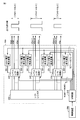
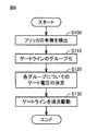
- 1 is an overall schematic diagram of a liquid crystal display device according to an embodiment. It is a figure for demonstrating the detailed structure of the gate driver in FIG. It is a flowchart for demonstrating the gate voltage control process in this Embodiment.
- FIG. 1 is a schematic configuration diagram of a general liquid crystal display device 10.
- liquid crystal display device 10 includes a liquid crystal display panel 100, a gate driver 200, a source driver 400, and a control device 300.
- the liquid crystal display panel 100 is an active matrix type liquid crystal panel in which pixel elements PX are arranged at intersections of a plurality of gate lines GL1 to GLx and a plurality of source lines SL1 to SLy arranged orthogonal to each other.
- the gate signals of the gate voltages VG1 to VGx are applied from the gate driver 200 to the gate lines GL1 to GLx, respectively.
- the adjusted source voltages VS1 to VSy are applied from the source driver 400 to the source lines SL1 to SLy, respectively.
- the pixel element PX disposed at the intersection of the gate line and the source line includes a liquid crystal cell whose transmitted light amount changes in response to the source voltage, and a source voltage from the source line to the liquid crystal cell. And a thin film transistor that switches between supply and shutoff. Then, by adjusting the magnitude of the source voltage and the application timing of the gate voltage, a desired transmitted light amount is realized for each pixel element, and an image of the entire screen is displayed.
- the gate driver 200 is controlled by a control signal SIG1 from the control device 300, and applies the gate voltage while sequentially scanning the gate voltage in the direction from the gate line GL1 to the gate line GLx (X direction in FIG. 1), for example.
- the source driver 400 is controlled by the control signal SIG2 from the control device 300, and controls and applies the magnitude of the source voltage to each source line in synchronization with the application of the gate voltage to each gate line. .
- Control device 300 receives video signal IMG to be displayed on liquid crystal display panel 100. Then, control device 300 generates control signals SIG1 and SIG2 based on received video signal IMG, and outputs them to gate driver 200 and source driver 400, respectively.
- FIG. 2 is a schematic diagram of an equivalent circuit of the pixel element PX.
- pixel element PX includes a thin film transistor TFT, a pixel capacitor Clc representing a liquid crystal cell, and an auxiliary capacitor Ccs.
- the source terminal of the thin film transistor TFT is connected to the source line SL, and the gate terminal is connected to the gate line GL.
- the one end of the pixel capacitor Clc is connected to the drain terminal of the thin film transistor TFT, and the other end is connected to the counter electrode COM.
- One end of the auxiliary capacitor Ccs is connected to the drain terminal of the thin film transistor TFT, and the other end is connected to the auxiliary capacitor signal line CS.
- the drain terminal of the thin film transistor TFT has a parasitic capacitance Cgd with respect to the gate line GL.
- the pixel capacitor Clc is charged by the adjusted source voltage applied to the source line SL. Then, the transmittance of the liquid crystal cell changes according to the magnitude of the source voltage applied to the pixel capacitor Clc.
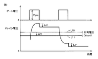
- FIG. 3 shows changes in the gate voltage applied to the gate line GL and the drain voltage appearing at the drain terminal of the thin film transistor TFT at this time.
- the field through voltage ⁇ V can be expressed as the following equation (1), where Vgpp is the voltage change of the gate signal.
- ⁇ V Cgd ⁇ Vgpp / (Clc + Cgd + Ccs) (1) If each parameter in the above is uniform for the entire liquid crystal panel, the counter voltage Vcom is adjusted in accordance with the field through voltage ⁇ V (from the broken line L10 to the solid line L11 in FIG. 3), thereby generating flicker. Can be suppressed.
- the thickness and the like of the liquid crystal cell are likely to vary between the central portion and the peripheral portion in the panel surface, and the pixel capacitance Clc of the liquid crystal cell may change accordingly. Then, the flicker distribution in the panel surface becomes non-uniform, and it may be difficult to suppress the flicker generation of the entire panel only by adjusting the counter voltage Vcom.
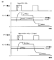
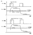
- FIG. 4 and 5 are diagrams for explaining gate voltage control in the present embodiment.
- FIG. 4 shows a method of adjusting the gate voltage when the liquid crystal cell thickness is thicker than the vicinity of the center of the liquid crystal panel
- FIG. 5 shows the gate when the liquid crystal cell thickness is thinner than the vicinity of the center of the liquid crystal panel. The voltage adjustment method is shown.
- the upper graph in FIG. 4 shows changes in gate voltage and drain voltage when the present embodiment is not applied, and the lower graph in FIG. 4 applies the present embodiment.
- the change in the gate voltage and the drain voltage in the case of the above is shown.
- the pixel capacitance Clc of the liquid crystal cell is expressed by the following formula (2), where ⁇ is the dielectric constant, S is the plate area, and d is the cell gap (that is, the cell thickness).
- the field voltage ⁇ V is set to be the same as the field voltage VFD (a) near the center.
- the field voltage ⁇ V decreases from the equation (1). That is, as can be seen in the upper graph of FIG. 5, when the liquid crystal cell thickness in the peripheral portion is thinner than the liquid crystal cell thickness near the center, the field voltage VFD (c) is equal to the field voltage VFD ( smaller than a).
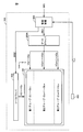
- FIG. 6 is an overall schematic diagram of a liquid crystal display device 10A according to the present embodiment.
- the gate driver 200 in the liquid crystal display device 10 shown in FIG. 1 is replaced with a gate driver 200A.
- description of elements overlapping with FIG. 1 will not be repeated.
- gate driver 200A divides a plurality of gate lines GL1 to GLx in liquid crystal display panel 100 into a plurality of groups, and drives by setting a gate voltage individually for each of the divided groups. Configured.
- the gate line includes a group near the center in the X direction (second group: GLn + 1 to GLm) and a group near the periphery (first group: GL1 to GLn, third group: GLm + 1).
- GLx are divided into three groups. Then, the gate driver 200A applies voltages for the first group as gate voltages VG1 to VGn, applies voltages for the second group as gate voltages VGn + 1 to VGm, and applies voltages for the third group to gate voltages VGm + 1 to VGm + 1 to VGm. Applied as VGx.
- the field-through voltage in the first and third group gate lines near the periphery approaches the field-through voltage in the second group gate line near the center (that is, the field-through voltage difference between the groups is
- Each gate voltage to be applied to the first and third group gate lines is set so as to be smaller.
- each gate line to the group in the gate driver 200A and the magnitude of the gate voltage in each group are set based on the control signal SIG1 from the control device 300.
- the grouping of the gate lines is determined based on the occurrence position of the flicker generated in the liquid crystal display panel 100.
- the flicker occurrence position is determined by the flicker occurrence state when an actual image is displayed when the liquid crystal display device 10A is assembled or adjusted.
- This determination may be made visually by an inspector or an adjuster.
- a flicker meter 450 as shown in FIG. 6 is used to scan in the X direction near the center of the Y direction in FIG.
- the luminance during the video display may be measured, and the control device 300 may determine using the detected luminance information or the detection signal FLK including information indicating the presence / absence of flicker based on the luminance information.
- the flicker meter scan may be automatically executed using a dedicated scanning device.
- 6 and 7 exemplify the case where a plurality of gate lines are divided into three groups, the number of groups may be divided into two groups according to the flicker occurrence state. It may be divided into more than three groups.
- FIG. 7 is a diagram for explaining a detailed configuration of the gate driver 200A in FIG.
- gate driver 200 ⁇ / b> A includes serial interface (SPI) circuit 210, shift register 220, level shift circuits 230, 240, 250, and voltage generators 231, 232, 241, 242. , 251, 252.
- SPI serial interface
- the SPI circuit 210 receives the control signal SIG1 from the control device 300 and, based on the received information, sends to the level shift circuits 230, 240, 250 and the voltage generators 231, 232, 241, 242, 251, 252. It is an interface circuit for outputting a signal.
- the SPI circuit 210 outputs, to the level shift circuits 230, 240, and 250, signals NUM1 to NUM3 that determine gate lines to be grouped in the respective level shift circuits based on the control signal SIG1.
- the signals NUM1 to NUM3 may set the number of gate lines to be included in each level shift circuit when grouping is performed with continuous gate lines, or may be set in each level shift circuit.
- the gate lines to be included may be set individually.
- the SPI circuit 210 outputs setting signals SET1 to SET3 for setting the gate voltage in each level shift circuit to the voltage generators 231, 232, 241, 242, 251, 252.
- the voltage generators 231 and 232 set the Hi voltage VGH1 and Lo voltage VGL1 of the gate signal set in the level shift circuit 230 based on the setting signal SET1 from the SPI circuit 210.
- the voltage generators 241 and 242 set the Hi voltage VGH2 and the Lo voltage VGL2 of the gate signal set in the level shift circuit 240 based on the setting signal SET2 from the SPI circuit 210.
- the voltage generators 251 and 252 set the Hi voltage VGH3 and Lo voltage VGL3 of the gate signal set in the level shift circuit 250 based on the setting signal SET3 from the SPI circuit 210.
- Each of the level shift circuits 230, 240, 250 uses the signal NUM from the SPI circuit 210 and the high voltage VGH, Lo voltage VGL of the gate signal from the corresponding voltage generation circuit to gate the corresponding gate line group. Generate a signal.
- the shift register 220 outputs drive signals to the level shift circuits 230, 240, and 250 so that gate signals are sequentially output from the gate lines GL1 to GLx according to a reference clock signal (not shown). Based on the drive signal from the shift register 220, the level shift circuits 230, 240, 250 output a gate signal having a predetermined voltage set as described above to a designated gate line.
- step S 100 the presence or absence of flicker is detected in control device 300 based on information from the flicker sensor shown in FIG.
- control device 300 divides the plurality of gate lines into a plurality of groups to be driven by each level shift circuit of the gate driver 200A based on the presence or absence of flicker.
- control device 300 determines the field-through voltage of each group from the flicker state. Then, in each voltage generation device of the gate driver 200A, the gate voltage set by each level shift circuit is adjusted based on the signal from the control device 300 so that the difference of the field through voltage between the groups becomes small.
- the plurality of gate lines are divided into a plurality of groups based on the flicker occurrence state, and the gate voltages of each group are individually set so that the field voltages are equal.
- a control device and a gate driver are configured. Accordingly, it is possible to reduce the occurrence of flicker due to the variation in the thickness of the liquid crystal cell of the liquid crystal display panel.
- 10A liquid crystal display device 100 liquid crystal display panel, 200, 200A gate driver, 210 SPI circuit, 220 shift register, 230, 240, 250 level shift circuit, 231, 232, 241, 242, 251, 252 voltage generator, 300 control device, 400 source driver, 450 flicker meter, COM counter electrode, CS auxiliary capacitance signal line, Ccs auxiliary capacitance, Cgd parasitic capacitance, Clc pixel capacitance, GL, GL1 to GLx gate line, PX pixel element, SL, SL1 to SLy source line, TFT thin film transistor.
Landscapes
- Engineering & Computer Science (AREA)
- Chemical & Material Sciences (AREA)
- Crystallography & Structural Chemistry (AREA)
- Physics & Mathematics (AREA)
- Computer Hardware Design (AREA)
- General Physics & Mathematics (AREA)
- Theoretical Computer Science (AREA)
- Liquid Crystal Display Device Control (AREA)
- Control Of Indicators Other Than Cathode Ray Tubes (AREA)
Abstract
液晶表示装置(10A)は、互いに直交配置された複数のゲートラインと複数のソースラインとの交点に画素素子が配置される、アクティブマトリクス型の液晶表示パネル(100)と、複数のゲートラインを駆動するゲートドライバ(200A)と、制御装置(300)とを備える。制御装置は、液晶表示パネルのフリッカの発生状態に基づいて、複数のゲートラインを複数のグループに分割する。ゲートドライバは、複数のグループに分割されたゲートラインについて、グループ間のフィードスルー電圧の差が小さくなるように、制御装置からの信号に基づいて設定したゲート電圧を用いて、ゲートラインを個別に駆動する。これにより、液晶表示装置において画面全体のフリッカを均一に調整する。
Description
本発明は、液晶表示装置およびその制御方法ならびにゲートドライバに関し、より特定的には、液晶表示装置の駆動制御に関する。
近年、液晶表示画面において、さらなる大画面化および高精細化の要求が高まっている。このような大画面化,高精細化を行なった場合には、一般的には、1画素領域全体のうち表示に有効な領域の面積比で表わされる開口率、および、画素における入射光量に対する出射光量の割合で表わされる透過率が低下する傾向にあることが知られている。このような大画面化,高精細化の一方で、画面の高輝度化がさらに要望されており、画素自体の設計における余裕度が小さくなっている。
また、画面の高開口率および高透過率を実現するための画素設計のトレードオフとして、画面内におけるフリッカ率の悪化が生じる可能性がある。
特開2000-137247号公報(特許文献1)は、アクティブマトリクス液晶表示装置において、ゲートドライバ出力の立下り波形を、線形関数,指数関数、または階段関数のいずれかの形態を用いて緩やかに変化させることによって、引き込み電圧(フィールドスルー電圧)を抑制し、フリッカおよび残像の発生を防止する技術を開示する。
また、国際公開第2009/133906号パンフレット(特許文献2)は、液晶表示装置において、走査信号線駆動回路からのゲートライン引き出し配線(映像信号線)の長さの違いに起因して生じるフリッカを低減するために、映像信号線の長さに応じて出力電圧を変化させる技術を開示する。
液晶表示装置が大画面化された場合、表示面の面積が大きくなるために、製造時における画面内のセル厚の不均一(ばらつき)が生じやすくなる。特に画面の中央部と周辺部との間において、セル厚に差が生じる可能性が高くなる。そうすると、画面の中央付近においてフリッカが小さくなるように調整した場合であっても、画面の周辺部においては十分にフリッカを抑制できず、画面全体としてフリッカを均一に調整できない状態となり得る問題があった。
上記の特許文献1および特許文献2の技術においては、このような製造時における画面内のセル厚のばらつきに伴うフリッカについては十分に考慮されていなかった。
本発明は、以上のような課題を解決するためになされたものであって、その目的は、画面全体としてフリッカを均一に調整可能な液晶表示装置を提供することである。
本発明による液晶表示装置は、互いに直交配置された複数のゲートラインと複数のソースラインとの交点に画素素子が配置された液晶表示パネルと、複数のゲートラインを駆動するゲートドライバとを備える。ゲートドライバは、複数のグループに分割された複数のゲートラインを、各グループ毎に個別のゲート電圧を用いて駆動するように構成される。
好ましくは、液晶表示装置は、ゲートドライバを制御する制御装置をさらに備える。制御装置は、複数のグループ間のフィールドスルー電圧の差が小さくなるように、複数のグループの各々についてゲート電圧を設定する。
好ましくは、制御装置は、複数のグループにおける液晶表示パネルの周辺部にある第1のグループのフィールドスルー電圧が、第1のグループよりも液晶表示パネルの中央部にある第2のグループのフィールドスルー電圧に近づくように、第1のグループのゲート電圧を設定する。
好ましくは、フィールドスルー電圧は液晶セルの厚さに応じて変化し、液晶セルの厚さが厚くなるほどフィールドスルー電圧が大きくなる傾向を有する。制御装置は、液晶セルの厚さが厚い場合には、液晶セルの厚さが薄い場合よりもゲート電圧の振幅が小さくなるようにゲート電圧を制御する。
好ましくは、ゲートドライバは、複数のグループに対応した複数のレベルシフト回路をそれぞれ含む。複数のレベルシフト回路の各々は、制御装置で設定されたゲート電圧に基づいて、対応するグループのゲートラインを駆動する。
好ましくは、制御装置は、液晶表示装置の表示状態に基づいてフリッカの有無を検出し、フリッカが生じているゲートライン位置に基づいて、複数のグループの各々に含まれるゲートラインを決定する。
本発明によるゲートドライバは、互いに直交配置された複数のゲートラインと複数のソースラインとの交点に画素素子が配置された液晶表示パネルの複数のゲートラインを駆動するためのものである。ゲートドライバは、複数のゲートラインを複数のグループに分割するための複数のレベルシフト回路と、複数のレベルシフト回路に対応して設けられ、複数のグループについてゲート電圧をそれぞれ個別に設定するための複数の電圧発生回路とを備える。
本発明による液晶表示装置の制御方法は、互いに直交配置された複数のゲートラインと複数のソースラインとの交点に画素素子が配置された液晶表示装置についての制御方法である。制御方法は、液晶表示装置の表示状態に基づいてフリッカの有無を検出するステップと、フリッカが生じているゲートライン位置に基づいて複数のゲートラインを複数のグループに分割するステップと、複数のグループ間のフィールドスルー電圧の差が小さくなるように、複数のグループの各々についてゲート電圧を個別に設定して、複数のゲートラインを駆動するステップとを備える。
本発明によれば、液晶表示装置において、画面全体としてフリッカを均一に調整することができる。
以下、本発明の実施の形態について、図面を参照しながら詳細に説明する。なお、図中同一または相当部分には同一符号を付してその説明は繰り返さない。
図1は、一般的な液晶表示装置10の概略構成図を示す。図1を参照して、液晶表示装置10は、液晶表示パネル100と、ゲートドライバ200と、ソースドライバ400と、制御装置300とを含む。
液晶表示パネル100は、互いに直交配置された複数のゲートラインGL1~GLxと複数のソースラインSL1~SLyとの交点に画素素子PXが配置された、アクティブマトリクス型の液晶パネルである。
ゲートラインGL1~GLxには、ゲートドライバ200からゲート電圧VG1~VGxのゲート信号がそれぞれ印加される。ソースラインSL1~SLyには、ソースドライバ400から、調整されたソース電圧VS1~VSyがそれぞれ印加される。
ゲートラインとソースラインとの交点に配置される画素素子PXには、図2で後述するように、ソース電圧に応答して透過光量が変化する液晶セルと、ソースラインから液晶セルへのソース電圧の供給および遮断を切換える薄膜トランジスタとが含まれる。そして、ソース電圧の大きさと、ゲート電圧の印加タイミングとを調整することによって、各画素素子について所望の透過光量を実現し、画面全体の映像が表示される。
ゲートドライバ200は、制御装置300からの制御信号SIG1により制御され、たとえば、ゲートラインGL1からゲートラインGLxの方向(図1のX方向)に、順次ゲート電圧を走査させながら印加する。
ソースドライバ400は、制御装置300からの制御信号SIG2により制御され、各ゲートラインへのゲート電圧の印加に同期させて、各ソースラインに対してソース電圧の大きさを個別に制御して印加する。
制御装置300は、液晶表示パネル100へ表示すべき映像信号IMGを受ける。そして、制御装置300は、受信した映像信号IMGに基づいて制御信号SIG1,SIG2を生成し、ゲートドライバ200およびソースドライバ400へそれぞれ出力する。
次に、図2を用いて、図1の液晶表示パネルの画素素子PXの構成について説明する。図2は、画素素子PXの等価回路の模式図である。
図2を参照して、画素素子PXは、薄膜トランジスタTFTと、液晶セルを表わす画素容量Clcと、補助容量Ccsとを含む。
薄膜トランジスタTFTのソース端子はソースラインSLに接続され、ゲート端子はゲートラインGLに接続される。
画素容量Clcの一方端は薄膜トランジスタTFTのドレイン端子に接続され、他方端は対向電極COMに接続される。補助容量Ccsの一方端は薄膜トランジスタTFTのドレイン端子に接続され、他方端は補助容量信号線CSに接続される。
なお、薄膜トランジスタTFTのドレイン端子は、ゲートラインGLに対して寄生容量Cgdを有する。
画素素子PXにおいて、ゲートラインGLにゲート電圧が印加されると、ソースラインSLに印加されている調整されたソース電圧によって画素容量Clcが充電される。そして、画素容量Clcに印加されたソース電圧の大きさに応じて、液晶セルの透過率が変化する。
このときの、ゲートラインGLへ印加されたゲート電圧と、薄膜トランジスタTFTのドレイン端子に現れるドレイン電圧の変化を図3に示す。
図2および図3を参照して、ゲートラインGLに対してゲート電圧が印加されて薄膜トランジスタTFTがターンオンしている間は、ソースラインSLに印加されているソース電圧がドレイン端子に現れる。その後、ゲート電圧の印加が終了すると、本来であればドレイン電圧は、印加されたソース電圧を保持するはずであるが、薄膜トランジスタTFTのゲート-ドレイン間に存在する寄生容量Cgdによって、ゲート信号の立下り時にドレイン端子の電位がΔVだけ低下する「フィールドスルー」と呼ばれる電圧変化が生じることが知られている。
このフィールドスルーによって生じる電圧変化ΔV(以下、「フィールドスルー電圧」とも称する。)のために、対向電極の電圧Vcomに対するドレイン端子の電位が変化してしまい、これが液晶表示パネルにおける焼き付きやフリッカの原因となり得る。そして、フィールドスルー電圧ΔVは、ゲート信号の電圧変化をVgppとすると、以下の式(1)のように表わすことができる。
ΔV=Cgd×Vgpp/(Clc+Cgd+Ccs) … (1)
上記における各パラメータが液晶パネル全体として均一である場合には、対向電圧Vcomを、フィールドスルー電圧ΔVに対応して(図3中の破線L10から実線L11へ)調整することによって、フリッカの発生を抑制することができる。
上記における各パラメータが液晶パネル全体として均一である場合には、対向電圧Vcomを、フィールドスルー電圧ΔVに対応して(図3中の破線L10から実線L11へ)調整することによって、フリッカの発生を抑制することができる。
しかしながら、特に大型の液晶表示パネルにおいては、パネル面内の中央部と周辺部とで液晶セルの厚さ等にばらつきが生じやすく、それによって液晶セルの画素容量Clcが変化し得る。そうすると、パネル面内におけるフリッカの分布が不均一となってしまうので、対向電圧Vcomの調整だけではパネル全体のフリッカの発生を抑制することが困難となり得る。
そこで、本実施の形態においては、ゲートラインに対して個別にゲート電圧を調整するゲート電圧制御を行なうことによって、液晶セル厚のばらつきに起因して生じ得る、特に液晶表示パネルのゲートラインに対して垂直方向についてのフリッカを低減する。
図4および図5は、本実施の形態におけるゲート電圧制御を説明するための図である。図4は、液晶セル厚が液晶パネルの中央付近よりも厚くなった場合のゲート電圧の調整手法を示し、一方、図5は液晶セル厚が液晶パネルの中央付近よりも薄くなった場合のゲート電圧の調整手法を示す。
図4を参照して、図4の上段のグラフは本実施の形態を適用していない場合のゲート電圧とドレイン電圧の変化を示しており、図4の下段のグラフは本実施の形態を適用した場合のゲート電圧とドレイン電圧の変化を示している。
ゲート電圧Vgppは、ゲート信号のHi電位(VGH)とLo電位(VGL)との差によって、Vgpp=VGH-VGLで定められる。
また、液晶セルの画素容量Clcは、誘電率をε、極板面積をS、セルギャップ(すなわち、セルの厚さ)をdとすると、以下の式(2)で表わされる。
Clc=ε×S/d … (2)
式(2)より、液晶セル厚dが大きくなると、画素容量Clcが小さくなる。これにより、結果として式(1)からフィールド電圧ΔVが大きくなる。すなわち、周辺部の液晶セル厚が中央付近の液晶セル厚よりも厚い場合には、フィールド電圧VFD(b)は、中央付近でのフィールド電圧VFD(a)よりも大きくなる。
式(2)より、液晶セル厚dが大きくなると、画素容量Clcが小さくなる。これにより、結果として式(1)からフィールド電圧ΔVが大きくなる。すなわち、周辺部の液晶セル厚が中央付近の液晶セル厚よりも厚い場合には、フィールド電圧VFD(b)は、中央付近でのフィールド電圧VFD(a)よりも大きくなる。
そこで、図4の下段のグラフのように、式(1)において、画素容量Clcの増加に対応してゲート電圧Vgppを小さく設定(Vgpp1=VGH1-VGL1<Vgpp)するように調整することによって、フィールド電圧ΔVが中央付近でのフィールド電圧VFD(a)と同じになるようにする。
一方、液晶セル厚dが小さくなると、式(2)より画素容量Clcが大きくなるので、結果として式(1)からフィールド電圧ΔVが小さくなる。すなわち、図5の上段のグラフに見られるように、周辺部の液晶セル厚が中央付近の液晶セル厚よりも薄い場合には、フィールド電圧VFD(c)は、中央付近でのフィールド電圧VFD(a)よりも小さくなる。
そのため、このような場合には、図5の下段のグラフのように、画素容量Clcの減少に対応して、フィールド電圧ΔVが中央付近でのフィールド電圧VFD(a)と同じになるようにゲート電圧Vgppを大きく設定(Vgpp2=VGH2-VGL2>Vgpp)するように調整が行われる。
次に、図6および図7を用いて本実施の形態に従う液晶表示装置についての詳細を説明する。
図6は、本実施の形態に従う液晶表示装置10Aの全体概略図である。液晶表示装置10Aは、図1で示した液晶表示装置10におけるゲートドライバ200がゲートドライバ200Aに置き換わったものとなっている。なお、図6において、図1と重複する要素の説明は繰り返さない。
図6を参照して、ゲートドライバ200Aは、液晶表示パネル100における複数のゲートラインGL1~GLxを複数のグループに分割し、分割された各グループ毎にゲート電圧を個別に設定して駆動するように構成される。
たとえば、図6の例においては、ゲートラインは、X方向の中央付近のグループ(第2グループ:GLn+1~GLm)、および、周辺付近のグループ(第1グループ:GL1~GLn,第3グループ:GLm+1~GLx)の3つのグループに分割される。そして、ゲートドライバ200Aは、第1グループについての電圧をゲート電圧VG1~VGnとして印加し、第2グループについての電圧をゲート電圧VGn+1~VGmとして印加し、第3グループについての電圧をゲート電圧VGm+1~VGxとして印加する。
そして、周辺付近の第1および第3グループのゲートラインにおけるフィールドスルー電圧が、中央付近の第2のグループのゲートラインにおけるフィールドスルー電圧に近づくように(すなわち、グループ間のフィールドスルー電圧の差が小さくなるように)、第1および第3のグループのゲートラインに印加する各ゲート電圧が設定される。
ゲートドライバ200Aにおける各ゲートラインのグループへの割り当て、および、各グループにおけるゲート電圧の大きさについては、制御装置300からの制御信号SIG1に基づいて設定される。
なお、ゲートラインのグルーピングについては、液晶表示パネル100において発生するフリッカの発生位置に基づいて決定される。このフリッカの発生位置は、液晶表示装置10Aの組立時あるいは調整時において、実際の映像を表示させたときのフリッカの発生状態により判定される。
この判定については、検査者または調整員の目視により行なってもよいが、たとえば、図6に示されるようなフリッカメータ450を用いて、図6のY方向の中央付近においてX方向にスキャンさせながら映像表示中の輝度を測定し、測定された輝度情報あるいは輝度情報に基づくフリッカの有無を示す情報を含む検出信号FLKを用いて、制御装置300が判定するようにしてもよい。また、フリッカメータのスキャンについても、スキャン用の専用の装置を用いて自動的に実行されてもよい。
なお、図6および図7においては、複数のゲートラインを3つのグループに分割する場合を例としているが、グループの数は、フリッカの発生状態に応じて、2つのグループに分割してもよいし、3つより多くのグループに分割してもよい。
図7は、図6におけるゲートドライバ200Aの詳細な構成を説明するための図である。図7を参照して、ゲートドライバ200Aは、シリアルインターフェース(Serial Peripheral Interface:SPI)回路210と、シフトレジスタ220と、レベルシフト回路230,240,250と、電圧発生装置231,232,241,242,251,252とを含む。
SPI回路210は、制御装置300からの制御信号SIG1を受信し、受信した情報に基づいて、レベルシフト回路230,240,250および電圧発生装置231,232,241,242,251,252に対して信号を出力するためのインターフェース回路である。
SPI回路210は、制御信号SIG1に基づいて、各レベルシフト回路にグルーピングされるべきゲートラインを定める信号NUM1~NUM3を、レベルシフト回路230,240,250にそれぞれ出力する。信号NUM1~NUM3は、たとえば、連続したゲートラインでグルーピングがなされる場合には各レベルシフト回路に含まれるべきゲートラインの数を設定するものであってもよいし、あるいは、各レベルシフト回路に含まれるべきゲートラインを個別に設定するものであってもよい。
またSPI回路210は、各レベルシフト回路におけるゲート電圧を設定するための設定信号SET1~SET3を、電圧発生装置231,232,241,242,251,252へ出力する。
電圧発生装置231,232は、SPI回路210からの設定信号SET1に基づいて、レベルシフト回路230において設定するゲート信号のHi電圧VGH1,Lo電圧VGL1を設定する。
電圧発生装置241,242は、SPI回路210からの設定信号SET2に基づいて、レベルシフト回路240において設定するゲート信号のHi電圧VGH2,Lo電圧VGL2を設定する。
電圧発生装置251,252は、SPI回路210からの設定信号SET3に基づいて、レベルシフト回路250において設定するゲート信号のHi電圧VGH3,Lo電圧VGL3を設定する。
レベルシフト回路230,240,250の各々は、SPI回路210からの信号NUMおよび対応する電圧発生回路からのゲート信号のHi電圧VGH,Lo電圧VGLを用いて、対応するゲートラインのグループについてのゲート信号を生成する。
シフトレジスタ220は、図示しない基準クロック信号に従って、ゲートラインGL1からGLxへと順次ゲート信号が出力されるように、レベルシフト回路230,240,250へ駆動信号を出力する。レベルシフト回路230,240,250は、シフトレジスタ220からの駆動信号に基づいて、指定されたゲートラインへ、上記のように設定された所定の電圧を有するゲート信号を出力する。
次に、図8のフローチャートを用いて、本実施の形態におけるゲート電圧制御処理を説明する。図8に示されたフローチャートに含まれる各ステップは、図6における制御装置300あるいはゲートドライバ200Aにおいて実行される。
図8を参照して、まず、ステップ(以下、ステップをSと略す。)100にて、制御装置300において、図6に示したフリッカセンサからの情報等に基づいて、フリッカの有無が検出される。
次に、S110にて、制御装置300において、フリッカの有無に基づいて、複数のゲートラインを、ゲートドライバ200Aの各レベルシフト回路で駆動すべき複数のグループに分割する。
そして、S120にて、制御装置300は、フリッカの状態から各グループのフィールドスルー電圧を判定する。そして、ゲートドライバ200Aの各電圧発生装置において、制御装置300からの信号に基づいて、グループ間のフィールドスルー電圧の差が小さくなるように、各レベルシフト回路によって設定するゲート電圧を調整する。
その後、S130にて、ゲートドライバ200Aのシフトレジスタからの駆動信号に応答して、各レベルシフト回路において、S120で設定されたゲート電圧を用いてゲートラインが順次駆動される。
以上のように、液晶表示装置において、フリッカの発生状態に基づいて、複数のゲートラインを複数のグループに分割するとともに、フィールド電圧が等しくなるように各グループのゲート電圧を個別に設定するように制御装置およびゲートドライバを構成する。これによって、液晶表示パネルの液晶セルの厚さのばらつきに伴うフリッカの発生を低減することが可能となる。
今回開示された実施の形態はすべての点で例示であって制限的なものではないと考えられるべきである。本発明の範囲は上記した説明ではなく、請求の範囲によって示され、請求の範囲と均等の意味および範囲内でのすべての変更が含まれることが意図される。
10,10A 液晶表示装置、100 液晶表示パネル、200,200A ゲートドライバ、210 SPI回路、220 シフトレジスタ、230,240,250 レベルシフト回路、231,232,241,242,251,252 電圧発生装置、300 制御装置、400 ソースドライバ、450 フリッカメータ、COM 対向電極、CS 補助容量信号線、Ccs 補助容量、Cgd 寄生容量、Clc 画素容量、GL,GL1~GLx ゲートライン、PX 画素素子、SL,SL1~SLy ソースライン、TFT 薄膜トランジスタ。
Claims (8)
- 液晶表示装置であって、
互いに直交配置された複数のゲートラインと複数のソースラインとの交点に画素素子が配置された液晶表示パネルと、
前記複数のゲートラインを駆動するゲートドライバとを備え、
前記ゲートドライバは、複数のグループに分割された前記複数のゲートラインを、各グループ毎に個別のゲート電圧を用いて駆動するように構成される、液晶表示装置。 - 前記ゲートドライバを制御する制御装置をさらに備え、
前記制御装置は、前記複数のグループ間のフィールドスルー電圧の差が小さくなるように、前記複数のグループの各々について前記ゲート電圧を設定する、請求項1に記載の液晶表示装置。 - 前記制御装置は、前記複数のグループにおける前記液晶表示パネルの周辺部にある第1のグループの前記フィールドスルー電圧が、前記第1のグループよりも前記液晶表示パネルの中央部にある第2のグループの前記フィールドスルー電圧に近づくように、前記第1のグループのゲート電圧を設定する、請求項2に記載の液晶表示装置。
- 前記フィールドスルー電圧は液晶セルの厚さに応じて変化し、前記液晶セルの厚さが厚くなるほど前記フィールドスルー電圧が大きくなる傾向を有し、
前記制御装置は、前記液晶セルの厚さが厚い場合には、前記液晶セルの厚さが薄い場合よりも前記ゲート電圧の振幅が小さくなるように前記ゲート電圧を制御する、請求項2に記載の液晶表示装置。 - 前記ゲートドライバは、前記複数のグループに対応した複数のレベルシフト回路をそれぞれ含み、
前記複数のレベルシフト回路の各々は、前記制御装置で設定されたゲート電圧に基づいて、対応するグループのゲートラインを駆動する、請求項2に記載の液晶表示装置。 - 前記制御装置は、前記液晶表示装置の表示状態に基づいてフリッカの有無を検出し、前記フリッカが生じているゲートライン位置に基づいて、前記複数のグループの各々に含まれるゲートラインを決定する、請求項2に記載の液晶表示装置。
- 互いに直交配置された複数のゲートラインと複数のソースラインとの交点に画素素子が配置された液晶表示パネルの前記複数のゲートラインを駆動するためのゲートドライバであって、
前記複数のゲートラインを複数のグループに分割するための複数のレベルシフト回路と、
前記複数のレベルシフト回路に対応して設けられ、前記複数のグループについてゲート電圧をそれぞれ個別に設定するための複数の電圧発生回路とを備える、ゲートドライバ。 - 互いに直交配置された複数のゲートラインと複数のソースラインとの交点に画素素子が配置された液晶表示装置の制御方法であって、
前記液晶表示装置の表示状態に基づいてフリッカの有無を検出するステップと、
前記フリッカが生じているゲートライン位置に基づいて、前記複数のゲートラインを複数のグループに分割するステップと、
前記複数のグループ間のフィールドスルー電圧の差が小さくなるように、前記複数のグループの各々についてゲート電圧を個別に設定して、前記複数のゲートラインを駆動するステップとを備える、液晶表示装置の制御方法。
Applications Claiming Priority (2)
| Application Number | Priority Date | Filing Date | Title |
|---|---|---|---|
| JP2012152442 | 2012-07-06 | ||
| JP2012-152442 | 2012-07-06 |
Publications (1)
| Publication Number | Publication Date |
|---|---|
| WO2014007199A1 true WO2014007199A1 (ja) | 2014-01-09 |
Family
ID=49881955
Family Applications (1)
| Application Number | Title | Priority Date | Filing Date |
|---|---|---|---|
| PCT/JP2013/067996 Ceased WO2014007199A1 (ja) | 2012-07-06 | 2013-07-01 | 液晶表示装置およびその制御方法、ならびにゲートドライバ |
Country Status (1)
| Country | Link |
|---|---|
| WO (1) | WO2014007199A1 (ja) |
Cited By (3)
| Publication number | Priority date | Publication date | Assignee | Title |
|---|---|---|---|---|
| JPWO2018012120A1 (ja) * | 2016-07-13 | 2018-11-01 | 富士電機株式会社 | パワーモジュール |
| CN110148387A (zh) * | 2019-05-21 | 2019-08-20 | 合肥奕斯伟集成电路有限公司 | 一种驱动电路的输出补偿方法及系统 |
| JPWO2019138740A1 (ja) * | 2018-01-12 | 2021-01-14 | ソニーセミコンダクタソリューションズ株式会社 | 液晶表示装置および液晶表示装置の駆動方法、並びに、電子機器 |
Citations (5)
| Publication number | Priority date | Publication date | Assignee | Title |
|---|---|---|---|---|
| JPH01167734A (ja) * | 1987-12-23 | 1989-07-03 | Matsushita Electric Ind Co Ltd | 液晶表示装置 |
| JP2003223148A (ja) * | 2002-01-29 | 2003-08-08 | Nec Kansai Ltd | 液晶表示装置の駆動方法および液晶表示装置 |
| JP2007183433A (ja) * | 2006-01-06 | 2007-07-19 | Canon Inc | 液晶表示装置及び制御方法 |
| JP2007323041A (ja) * | 2006-06-02 | 2007-12-13 | Lg Phillips Lcd Co Ltd | 液晶表示装置及びその駆動方法 |
| JP2010223995A (ja) * | 2009-03-19 | 2010-10-07 | Toppoly Optoelectronics Corp | 液晶表示装置の駆動方法及び液晶表示装置 |
-
2013
- 2013-07-01 WO PCT/JP2013/067996 patent/WO2014007199A1/ja not_active Ceased
Patent Citations (5)
| Publication number | Priority date | Publication date | Assignee | Title |
|---|---|---|---|---|
| JPH01167734A (ja) * | 1987-12-23 | 1989-07-03 | Matsushita Electric Ind Co Ltd | 液晶表示装置 |
| JP2003223148A (ja) * | 2002-01-29 | 2003-08-08 | Nec Kansai Ltd | 液晶表示装置の駆動方法および液晶表示装置 |
| JP2007183433A (ja) * | 2006-01-06 | 2007-07-19 | Canon Inc | 液晶表示装置及び制御方法 |
| JP2007323041A (ja) * | 2006-06-02 | 2007-12-13 | Lg Phillips Lcd Co Ltd | 液晶表示装置及びその駆動方法 |
| JP2010223995A (ja) * | 2009-03-19 | 2010-10-07 | Toppoly Optoelectronics Corp | 液晶表示装置の駆動方法及び液晶表示装置 |
Cited By (4)
| Publication number | Priority date | Publication date | Assignee | Title |
|---|---|---|---|---|
| JPWO2018012120A1 (ja) * | 2016-07-13 | 2018-11-01 | 富士電機株式会社 | パワーモジュール |
| JPWO2019138740A1 (ja) * | 2018-01-12 | 2021-01-14 | ソニーセミコンダクタソリューションズ株式会社 | 液晶表示装置および液晶表示装置の駆動方法、並びに、電子機器 |
| JP7341895B2 (ja) | 2018-01-12 | 2023-09-11 | ソニーセミコンダクタソリューションズ株式会社 | 液晶表示装置および液晶表示装置の駆動方法、並びに、電子機器 |
| CN110148387A (zh) * | 2019-05-21 | 2019-08-20 | 合肥奕斯伟集成电路有限公司 | 一种驱动电路的输出补偿方法及系统 |
Similar Documents
| Publication | Publication Date | Title |
|---|---|---|
| US9182805B2 (en) | Display device and method to control driving voltages based on changes in display image frame frequency | |
| KR101495695B1 (ko) | 능동 매트릭스 디스플레이 패널을 구동하는 방법, 장치 및 디스플레이 | |
| KR101396688B1 (ko) | 액정표시장치 및 그 구동방법 | |
| US20100103085A1 (en) | Horizontal Electric Field Liquid Crystal Display | |
| KR20160042014A (ko) | 어레이 기판 및 액정 디스플레이 장치 | |
| CN104240661B (zh) | 极性反转驱动方法、极性反转驱动装置和显示设备 | |
| US10656477B2 (en) | Liquid crystal display device | |
| WO2017150175A1 (ja) | 表示装置及び表示装置の検査方法 | |
| JP5940297B2 (ja) | 液晶ディスプレーにおけるゲートライン駆動方法及びゲートライン駆動装置 | |
| KR20100056318A (ko) | 액정표시장치 | |
| KR101232178B1 (ko) | 평판표시장치의 표시결함 보상방법 및 장치 | |
| KR101992885B1 (ko) | 액정 표시장치의 구동장치와 그 구동방법 | |
| WO2014007199A1 (ja) | 液晶表示装置およびその制御方法、ならびにゲートドライバ | |
| KR101977252B1 (ko) | 액정표시장치와 그 구동 방법 | |
| US8411008B2 (en) | Liquid crystal display having a plurality of common voltages applied during different driving time and driving method thereof | |
| KR101493526B1 (ko) | 액정표시장치 | |
| KR20150107484A (ko) | 액정표시장치 및 그 구동방법 | |
| KR20030095112A (ko) | 액정표시소자의 구동방법 및 장치 | |
| KR102019766B1 (ko) | 액정표시장치 및 그 구동 방법 | |
| TWI435298B (zh) | 電泳顯示器的驅動方法及饋通電壓的量測方法 | |
| WO2009128281A1 (ja) | 液晶表示装置の駆動回路 | |
| WO2014141378A1 (ja) | 画像表示装置及びその駆動方法 | |
| CN112201187B (zh) | 一种显示面板仿真测试方法 | |
| KR20120073824A (ko) | 액정표시장치 | |
| JP5512788B2 (ja) | 液晶表示装置の表示検査方法 |
Legal Events
| Date | Code | Title | Description |
|---|---|---|---|
| 121 | Ep: the epo has been informed by wipo that ep was designated in this application |
Ref document number: 13813529 Country of ref document: EP Kind code of ref document: A1 |
|
| NENP | Non-entry into the national phase |
Ref country code: DE |
|
| 122 | Ep: pct application non-entry in european phase |
Ref document number: 13813529 Country of ref document: EP Kind code of ref document: A1 |
|
| NENP | Non-entry into the national phase |
Ref country code: JP |