WO2013183290A1 - 光学的分析用の測定デバイス - Google Patents
光学的分析用の測定デバイス Download PDFInfo
- Publication number
- WO2013183290A1 WO2013183290A1 PCT/JP2013/003532 JP2013003532W WO2013183290A1 WO 2013183290 A1 WO2013183290 A1 WO 2013183290A1 JP 2013003532 W JP2013003532 W JP 2013003532W WO 2013183290 A1 WO2013183290 A1 WO 2013183290A1
- Authority
- WO
- WIPO (PCT)
- Prior art keywords
- silica glass
- measuring device
- flat plate
- inorganic
- flow path
- Prior art date
- Legal status (The legal status is an assumption and is not a legal conclusion. Google has not performed a legal analysis and makes no representation as to the accuracy of the status listed.)
- Ceased
Links
Images








Classifications
-
- G—PHYSICS
- G01—MEASURING; TESTING
- G01N—INVESTIGATING OR ANALYSING MATERIALS BY DETERMINING THEIR CHEMICAL OR PHYSICAL PROPERTIES
- G01N21/00—Investigating or analysing materials by the use of optical means, i.e. using sub-millimetre waves, infrared, visible or ultraviolet light
- G01N21/01—Arrangements or apparatus for facilitating the optical investigation
- G01N21/03—Cuvette constructions
- G01N21/05—Flow-through cuvettes
-
- B—PERFORMING OPERATIONS; TRANSPORTING
- B01—PHYSICAL OR CHEMICAL PROCESSES OR APPARATUS IN GENERAL
- B01L—CHEMICAL OR PHYSICAL LABORATORY APPARATUS FOR GENERAL USE
- B01L3/00—Containers or dishes for laboratory use, e.g. laboratory glassware; Droppers
- B01L3/50—Containers for the purpose of retaining a material to be analysed, e.g. test tubes
- B01L3/502—Containers for the purpose of retaining a material to be analysed, e.g. test tubes with fluid transport, e.g. in multi-compartment structures
- B01L3/5027—Containers for the purpose of retaining a material to be analysed, e.g. test tubes with fluid transport, e.g. in multi-compartment structures by integrated microfluidic structures, i.e. dimensions of channels and chambers are such that surface tension forces are important, e.g. lab-on-a-chip
- B01L3/502707—Containers for the purpose of retaining a material to be analysed, e.g. test tubes with fluid transport, e.g. in multi-compartment structures by integrated microfluidic structures, i.e. dimensions of channels and chambers are such that surface tension forces are important, e.g. lab-on-a-chip characterised by the manufacture of the container or its components
-
- B—PERFORMING OPERATIONS; TRANSPORTING
- B01—PHYSICAL OR CHEMICAL PROCESSES OR APPARATUS IN GENERAL
- B01L—CHEMICAL OR PHYSICAL LABORATORY APPARATUS FOR GENERAL USE
- B01L2300/00—Additional constructional details
- B01L2300/06—Auxiliary integrated devices, integrated components
- B01L2300/0627—Sensor or part of a sensor is integrated
- B01L2300/0654—Lenses; Optical fibres
-
- B—PERFORMING OPERATIONS; TRANSPORTING
- B01—PHYSICAL OR CHEMICAL PROCESSES OR APPARATUS IN GENERAL
- B01L—CHEMICAL OR PHYSICAL LABORATORY APPARATUS FOR GENERAL USE
- B01L2300/00—Additional constructional details
- B01L2300/08—Geometry, shape and general structure
- B01L2300/0809—Geometry, shape and general structure rectangular shaped
- B01L2300/0816—Cards, e.g. flat sample carriers usually with flow in two horizontal directions
-
- B—PERFORMING OPERATIONS; TRANSPORTING
- B01—PHYSICAL OR CHEMICAL PROCESSES OR APPARATUS IN GENERAL
- B01L—CHEMICAL OR PHYSICAL LABORATORY APPARATUS FOR GENERAL USE
- B01L2300/00—Additional constructional details
- B01L2300/08—Geometry, shape and general structure
- B01L2300/0861—Configuration of multiple channels and/or chambers in a single devices
- B01L2300/0867—Multiple inlets and one sample wells, e.g. mixing, dilution
-
- B—PERFORMING OPERATIONS; TRANSPORTING
- B01—PHYSICAL OR CHEMICAL PROCESSES OR APPARATUS IN GENERAL
- B01L—CHEMICAL OR PHYSICAL LABORATORY APPARATUS FOR GENERAL USE
- B01L2400/00—Moving or stopping fluids
- B01L2400/08—Regulating or influencing the flow resistance
- B01L2400/084—Passive control of flow resistance
Definitions
- the present invention relates to a measuring device for optical analysis. More specifically, the present invention relates to a measurement device for optical analysis that uses light having a short wavelength as an excitation wavelength and a detection wavelength. In particular, the present invention relates to a microchannel device.
- Patent Document 1 discloses a fine particle analysis apparatus in liquid that solves the problems related to biohazards of conventional flow cytometers and cell sorters.
- Patent Document 1 discloses an in-liquid microparticle analysis apparatus, a means for mounting a flow cell having a flow channel for flowing a sample liquid containing fine particles, and a flow channel of the flow cell.
- a flow cell is a plate-like substrate having a flow path formed therein, and a reflective surface is formed on a side surface of the flow path, and the reflective surface is a flow cell of the flow cell.
- the light traveling in the in-plane direction of the substrate is guided to a specific area on the surface of the flow cell, and the photodetector detects the light emitted from the specific area to the outside.
- Japanese Patent Application Laid-Open No. 2010-181349 describes that a side signal light can be detected by forming a reflective surface on a flat substrate of a flow cell.
- the flow cell is made of resin, it does not transmit a short wavelength laser. For this reason, there is a problem in that transmission measurement using a short wavelength laser cannot be performed.
- a material that is most suitable as a member of a measuring device for optical analysis for performing excitation and transmission measurement using a light beam with a short wavelength is silica glass (quartz glass) or the like. Therefore, from an optical point of view, it is preferable that all members of the optical analysis measuring device are made of silica glass or the like.
- quartz glass is very hard and has a very high softening point compared to resin. Therefore, especially as a flat substrate member of a microchannel device, quartz glass has a problem in that it is very difficult to efficiently manufacture a highly accurate channel and the manufacturing cost increases. It was.
- An object of the present invention is to provide a measuring device for optical analysis that can be measured under optimum conditions and can be manufactured with high accuracy and relatively easily at low cost.
- the measuring device of the present invention includes a resin member, a transparent member that transmits light having a wavelength of 450 nm or less attached to the resin member, and a flow path that passes through the resin member while contacting the transparent member.
- the transparent member is more preferably one that transmits light having a wavelength of 410 nm or less.
- the transparent member is preferably colorless and transparent.
- the material for the transparent member may be either an inorganic material or an organic material.
- any one of an inorganic member and an organic member may be used independently, and both may be used in combination. When the inorganic member and the organic member are combined, different materials can be used on the incident side and the detector side in one detector as an example of the combination mode.
- a plurality of detection units may be provided in one measurement device, and different materials may be used depending on the detection units.
- the transparent member that is an organic substance is a transparent resin member.
- the transparent resin member has a transmittance for light having a wavelength of 220 nm or more and 450 nm or less, for example, 50% or more, and preferably 80% or more.
- a measuring device for optical analysis includes a resin member, an inorganic member attached to the resin member, and a flow path that passes through the resin member while contacting the inorganic member.
- a measurement device for optical analysis can be realized easily and at a lower cost than when the entire flow path is formed of an inorganic material. I can do it. Further, the transmission measurement can be reliably performed.
- the resin member may be a flat resin substrate.
- the inorganic member may be attached by being fitted in a fitting hole or notch formed in a part of the resin member.
- the inorganic member is preferably attached so that the combined shape of the inorganic member and the resin member is a flat plate shape. In this case, it is preferable that there is no surface step at the boundary between the inorganic member and the resin member on the outer surface of the measurement device, or the surface step is greater than 0 ⁇ m and not more than 100 ⁇ m.
- the resin member, the flow path is provided.
- both surfaces may be integrated to define the flow path space.
- at least a part of the surface of the inorganic member that defines the flow path space is referred to as a flow path side surface of the inorganic member.
- a recess may be formed on the surface of the inorganic member.
- the concave surface of the inorganic member is continuous with at least one of the surfaces of the resin member forming the flow path, thereby defining the flow path space integrally with the surface of the flow path.
- the flow path side surface of the inorganic member is allowed to be flush with the surface of the resin member connected to it (that is, the step is 0 ⁇ m) or has a step of 0 ⁇ m to 100 ⁇ m, preferably 0 ⁇ m to 50 ⁇ m. To do. Since the level difference between the resin member surface and the inorganic member surface is within the above range, the liquid flow is not easily disturbed even in the vicinity of the boundary between the resin member and the inorganic member in the flow path. Therefore, even when the liquid flow is a laminar flow, the laminar flow state can be preferably maintained.
- the inorganic member is preferably attached to the resin member so that the surface of the inorganic member and the surface of the resin member are in contact with each other with almost no gap. That is, it is preferable that the fitting hole or the notch for fitting the inorganic member into the resin member is formed to have a shape corresponding to the shape of the inorganic member.
- the measuring device for optical analysis according to the second invention is the measuring device for optical analysis according to one aspect, wherein the inorganic member has a tapered portion.
- the inorganic member can be securely fitted to the resin member by the tapered portion of the inorganic member and can be integrally attached.
- the gap between the resin member and the inorganic member can be made zero as much as possible, and leakage of the medium passing through the flow path can be prevented.
- the inorganic member having the tapered portion preferably has a shape having an axis in the thickness direction of the device.
- the taper portion has an inclined surface that is inclined with respect to the axis.
- the inorganic member having the tapered portion may be in the shape of a truncated cone, for example, or may be a combined shape of a columnar portion and a truncated cone portion that is gradually tapered in the axial direction from the columnar portion. There may be.
- the angle of the inclined surface of the tapered portion with respect to the axis is theoretically in the range of more than 0 degrees and less than 90 degrees.
- the angle of the inclined surface of the tapered portion of the inorganic member is preferably not less than a certain degree. From such a viewpoint, the angle of the inclined surface is, for example, more than 0 degree and less than 90 degrees. It may be. Further, in consideration of prevention of extraction after fitting into the resin member, the angle of the inclined surface tends to be preferably small. From such a viewpoint, for example, more than 0 degree and 60 degrees or less, preferably 5 degrees it may be less than 30 degrees.
- the measuring device for optical analysis according to the third invention is the measuring device for optical analysis according to one aspect or the second invention, wherein the inorganic member has a circular cross section.
- the inorganic member has a circular cross section, it is easy to attach to the plastic resin member.
- the circumference has a tapered portion, pressure is uniformly applied to the circumference, so that generation of a gap can be prevented and leakage of the medium passing through the flow path can be surely prevented.
- the measuring device for optical analysis according to the fourth invention is the measuring device for optical analysis according to one aspect or the second invention, wherein the inorganic member has a rectangular cross section.
- the inorganic member since the inorganic member has a rectangular shape, the directionality of the flow path can be easily adjusted. As a result, the flow path between the resin member and the inorganic member can be reliably adjusted.
- a measuring device for optical analysis according to a fifth invention is the measuring device for optical analysis according to any one of the fourth invention from one aspect, wherein the inorganic member is integrally formed with the resin member. .
- the resin is molded integrally with the inorganic member by surrounding the inorganic member with the molten resin and curing it at the time of injection molding of the resin member. For this reason, mass production of measuring devices for optical analysis can be realized at low cost.
- a measuring device for optical analysis according to a sixth invention is the measuring device for optical analysis according to the fifth invention, wherein the inorganic member has a convex shape for preventing extraction from the resin member.
- the inorganic member since the inorganic member has a convex portion for preventing extraction from the resin member, the inorganic member can be securely attached to the resin member. Further, since the inorganic member can be prevented from being pulled out from the resin member, a stable measuring device for optical analysis can be formed.
- the convex shape portion for preventing the extraction of the inorganic member may be a shape protruding from the surface of the inorganic member that contacts the resin member.
- the measuring device for optical analysis according to the seventh invention is the measuring device for optical analysis according to the fifth or sixth invention, wherein the inorganic member is an arithmetic average roughness for preventing extraction from the resin member. Has a surface of Ra 0.1 ⁇ m or more and 1 ⁇ m or less.
- the inorganic member has a surface that contacts the resin member formed as an extraction preventing surface.
- the extraction preventing surface has an arithmetic average roughness Ra of 0.1 ⁇ m to 1 ⁇ m, preferably 0.2 ⁇ m to 1 ⁇ m.
- the extraction preventing surface may be subjected to a surface treatment for preventing the inorganic member from being extracted. For example, a non-slip pattern such as a streak may be formed in a direction non-parallel to the direction in which the extraction is to be prevented (specifically, the direction parallel to the shaft of the inorganic member or the thickness direction of the measurement device).
- the inorganic member since the inorganic member has a surface with an arithmetic average roughness Ra for preventing extraction from the resin member of 0.1 ⁇ m or more and 1 ⁇ m or less, the inorganic member can be prevented from being extracted from the resin member.
- the arithmetic average roughness Ra is based on a standard defined in JIS B 0601: 2001.
- the measuring device for optical analysis according to the eighth invention is the measuring device for optical analysis according to any one of the seventh invention from one aspect, wherein the resin member comprises the first resin member and the second resin member.
- the inorganic member is composed of a first inorganic member attached to the first resin member and a second inorganic member attached to the second resin member, and the flow path includes a recess formed in the first resin member. The first inorganic member, the second resin member, and the surface of the second inorganic member are combined with each other.
- the flow path can be easily formed by bonding the first resin member to which the first inorganic member is attached and the second resin member to which the second inorganic member is attached.
- the cross section of the flow path is rectangular.
- the inorganic member attached to the second resin member is preferably disposed so as not to contact the first resin member.
- the fixation between the inorganic member and the resin member tends to be weaker than the fixation between the resin member and the resin member.
- the measuring device of the present invention is particularly useful when the wavelength of light used for optical measurement is a short wavelength.
- the short wavelength in the present invention is specifically a wavelength of 450 nm or less, preferably 410 nm or less.
- the inorganic member has a transmittance for light having a wavelength used for optical measurement of, for example, 60% or more.
- the above transmittance can be obtained by measuring with a UV-Vis-NIR spectrophotometer Cary 6000i manufactured by Agilent Technologies.
- a measuring device for optical analysis according to a ninth aspect of the invention is the measuring device for optical analysis according to any one of the eighth aspect of the invention, wherein the inorganic member is for light of a wavelength used for optical measurement. and more preferably transmittance of 80% or more.
- the inorganic member since the inorganic member has a transmittance of 80% or more with respect to the wavelength of light used for optical measurement, the transmission measurement can be reliably performed.
- a measuring device for optical analysis according to a tenth invention is the measuring device for optical analysis according to any one of the ninth invention from one aspect, wherein the inorganic member is silica glass.
- the inorganic member is silica glass, the transmission measurement can be reliably performed.
- An optical analysis measurement device is the optical analysis measurement device according to any one of the tenth aspect of the invention from one aspect, wherein the inorganic member emits light having a wavelength of 180 nm or more and 1000 nm or less.
- % Is a synthetic silica glass that transmits 80% or more of light having a wavelength of 1000 nm to 2500 nm.
- the inorganic member is a synthetic silica glass that transmits 90% or more of light having a wavelength of 180 nm or more and 1000 nm or less, and 80% or more of light having a wavelength of 1000 nm or more and 2500 nm or less. Can be implemented.
- a measurement device for optical analysis according to a twelfth aspect of the invention is the optical analysis measurement device according to any of the eleventh aspects of the invention, wherein the inorganic member has two parallel mirror surfaces, and the mirror surface One side of this is in contact with the flow path and the other side of the mirror surface is in contact with the outside air.
- the inorganic member has two parallel mirror surfaces, and one of the mirror surfaces is in contact with the flow path and the other of the mirror surfaces is in contact with the outside air, the transmission measurement can be reliably performed.
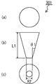
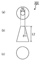
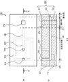
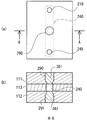
- FIG. 1 is a schematic diagram illustrating an example of a measurement device (microchannel device) according to the first embodiment, and FIGS. 2 and 3 are schematic enlarged views of a silica glass portion of the measurement device of FIG. is there.
- FIG. 1A shows a plan view of the measuring device as viewed from above
- FIG. 1B shows a cross section taken along the line AA in FIG. 2 (a) and 3 (a) show a top view of the silica glass chip constituting the silica glass portion
- FIGS. 2 (b) and 3 (b) show a side view of the silica glass chip
- FIGS. 2 (b) and 3 (b) show a side view of the silica glass chip.
- C) and FIG.3 (c) show the bottom (lower surface) view of a silica glass chip
- the upper surface and the lower surface of the silica glass chip are a pair of opposing surfaces of the surfaces constituting the silica glass chip, and the silica glass chip is incorporated in the microchannel device for measurement. When provided, it refers to a pair of surfaces consisting of a surface to be an incident surface for measurement light and an opposing surface thereof.
- the measuring device 100 is formed by bonding a first flat plate 111 and a second flat plate 112 together.
- the 1st flat plate 111 and the 2nd flat plate 112 are comprised with a plastic resin except the silica glass part 300 mentioned later.
- the measuring device 100 mainly includes three regions of a liquid feeding / merging portion, a detecting portion, and a discharging portion.
- the measuring device 100 has a first liquid inlet (inlet) 210 and a second liquid inlet (inlet) 230 on the surface of the liquid feeding / merging portion.
- the first liquid introduction port 210 and the second liquid introduction port 230 communicate with the flow path (channel) 220, and the flow path 220 further communicates with the flow path 240.
- the first liquid inlet 210 and the second liquid inlet 230 are formed in the first flat plate 111.
- the first liquid introduction port 210 and the second liquid introduction port 230 lead to a through hole extending in the thickness direction of the first flat plate 111.
- the recesses of the flow paths 220 and 240 are communicated with the respective through-holes and are designed so that the liquid flow from the first liquid introduction port 210 and the liquid flow from the second liquid introduction port 230 are merged.
- the first flat plate 111 and the second flat plate 112 are bonded together to form the flow paths 220 and 240.
- the flow path 240 is formed so that a pipe cross section becomes small as it approaches a detection part.
- fitting holes 250 and 251 for fitting the silica glass part 300 are formed in the first flat plate 111 and the second flat plate 112 so as to communicate with the flow path 240.
- tip 302 which comprise the silica glass part 300 are each engage
- tip 302 are attached to the 1st flat plate 111 and the 2nd flat plate 112, respectively.
- concave portions are formed at positions corresponding to each other on both surfaces of the first flat plate 111 and the second flat plate 112, and both concave portions constitute a part of the flow path 240.
- the terminal end of the flow path 240 on the side surface of the measuring device 100 constitutes an outlet (outlet) 245.
- the silica glass chip 301 has a truncated inverted conical shape.
- the length L1 of the silica glass chip 301 is 1 mm
- the small diameter R2 is 0.2 mm
- the taper inclination ⁇ 1 of the side surface with respect to the axial center direction of the silica glass chip 301 is for example, 30 degrees.
- the silica glass chip 302 has a truncated cone shape.
- the length L2 of the silica glass chip 302 is 0.875 mm, the small diameter R2 is 0.2 mm, and the taper slope ⁇ 1 of the side surface with respect to the axial direction of the silica glass chip 302 (that is, the vertical direction in FIG. 3B). Is, for example, 30 degrees.
- the upper and lower surfaces of the silica glass chips 301 and 302 are irradiated with measurement light.
- arithmetic mean roughness Ra of the said upper and lower surfaces is 0.2 micrometer or less, for example, Preferably it is 0.1 micrometer or less, More preferably, it is 0.05 micrometer or less.
- the side surface is formed with a rougher surface than the upper and lower surfaces.
- the arithmetic average roughness Ra of the side surface formed of a rougher surface is, for example, 0.1 ⁇ m or more and 1 ⁇ m or less, preferably 0.2 ⁇ m or more and 1 ⁇ m or less, and more preferably 0.3 ⁇ m or more and 0.7 ⁇ m or less.
- the silica glass chip 301 shown in FIG. 2 is press-fitted into the fitting hole 250 of the first flat plate 111.
- the first flat plate 111 no gap is formed between the fitting hole 250 and the silica glass chip 301, and the height difference between the small diameter surface of the silica glass chip 301 and the surface of the first flat plate 111 is 0 ⁇ m or more. It is formed to be within a range of 50 ⁇ m or less. Since the gap between the fitting hole 250 of the first flat plate 111 and the silica glass chip 301 is not formed, leakage of the liquid in the flow path 240 does not occur.
- the liquid flow in the channel 240 can be maintained as a laminar flow. .
- the silica glass chip 302 shown in FIG. 3 is press-fitted into the fitting hole 251 of the second flat plate 112.
- a gap between the fitting hole 251 and the silica glass chip 302 is not formed, and the flow path 240 formed on the small diameter surface of the silica glass chip 302 and the surface of the second flat plate 112.
- the height difference from the bottom surface of the recess is in the range of 0 ⁇ m to 50 ⁇ m. Since the gap between the fitting hole 251 of the second flat plate 112 and the silica glass chip 302 is not formed, the liquid in the flow path 240 does not leak.
- the difference in height between the small diameter surface of the silica glass chip 302 and the bottom surface of the concave portion of the flow channel 240 formed on the surface of the second flat plate 112 is in the range of 0 ⁇ m or more and 50 ⁇ m or less.
- the flow can be maintained as a laminar flow.
- the first liquid introduced from the first liquid inlet 210 passes through the flow path 220, and the second liquid introduced from the second liquid inlet 230 passes through another flow path 220.
- the liquid flow of the first liquid and the liquid flow of the second liquid that have passed through the flow path 220 merge at the boundary between the flow path 220 and the flow path 240 to form a laminar flow in the flow path 240.
- the laminar flow of the first liquid and the second liquid is guided to the detection unit, passes through the silica glass unit 300 while maintaining the laminar flow state, and subjected to optical measurement, and then the discharge port of the discharge unit It is discharged from H.245.
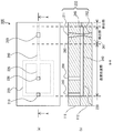
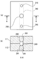
- FIG. 4 is a schematic view showing another example of the measuring device according to the first embodiment
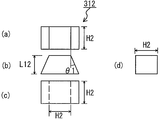
- FIGS. 5 and 6 are schematic enlarged views of the silica glass portion of the measuring device of FIG.
- FIG. 4 (a) shows a plan view (top view) of the measuring device as viewed from above
- FIG. 4 (b) shows a cross section taken along the line AA in FIG. 4 (a).
- 5 (a) and 6 (a) are top views of the silica glass chip
- FIGS. 5 (b) and 6 (b), 5 (d) and 6 (d) are side views of the silica glass chip.
- 5 (c) and FIG. 6 (c) show bottom views of the silica glass chip.
- the measuring device 100 includes a silica glass portion 310 that is square in top view instead of the silica glass portion 300 that is circular in top view.
- the silica glass chip 311 has a hexahedral shape provided with grooves.
- the hexahedron has a rectangular shape in which the upper surface (see FIG. 5 (a)) and the lower surface (see FIG. 5 (c)) have different sizes, and one pair of side surfaces of the two opposing side surfaces has the same shape.
- the other pair of side surfaces is formed of the same rectangular shape (see FIG. 5D).
- a groove having a width H3 is formed on the lower surface of the silica glass chip 311. Thereby, the lower part of the other pair of side surfaces has a rectangular cutout having a width H3 (see FIG.
- the length L11 of the silica glass chip 311 is 1 mm
- the width H1 is 4 mm
- the width H2 is 2 mm
- the groove width H3 is 0.19 mm.
- the taper inclination ⁇ 1 of the side surface with respect to the axial direction of the silica glass chip 311 is, for example, 30 degrees.
- the silica glass chip 312 has a hexahedral shape.
- the hexahedron has a rectangular shape in which the upper surface (see FIG. 6A) and the lower surface (see FIG. 6C) have different sizes, and one pair of side surfaces of the two opposing side surfaces has the same shape.
- the other pair of side surfaces is formed of the same rectangular shape (see FIG. 6D).
- the length L12 of the silica glass chip 312 is 0.875 mm, and the width H2 is 2 mm.
- the taper slope ⁇ 1 of the side surface with respect to the axial direction of the silica glass chip 312 (that is, the vertical direction in FIG. 6B) is, for example, 30 degrees.
- the silica glass chip 311 shown in FIG. As a result, in the first flat plate 111, a gap between the fitting hole 260 and the silica glass chip 311 is not formed, and the height difference between the lower surface of the silica glass chip 311 and the surface of the first flat plate 111 is in the range of 0 ⁇ m or more and 50 ⁇ m or less. It is formed to be inside. Since the gap between the fitting hole 260 of the first flat plate 111 and the silica glass chip 311 is not formed, the liquid in the flow path 240 does not leak.
- the liquid flow in the flow path 240 can be maintained as a laminar flow.
- the difference in height between the top surface of the silica glass chip 312 and the bottom surface of the recess of the flow channel 240 formed on the surface of the second flat plate 112 is in the range of 0 ⁇ m or more and 50 ⁇ m or less. It can be maintained as a laminar flow.
- the entire silica glass chip 312 is press-fitted into the fitting hole 261 of the second flat plate 112, and a part of the silica glass chip 311 is also press-fitted by bonding with the first flat plate 111. .
- the upper surface of the silica glass chip 312 and the lower surface of the silica glass chip 311 contact
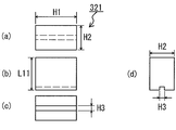
- FIG. 7 is a schematic view showing still another example of the measurement device according to the first embodiment
- FIGS. 8 and 9 are schematic enlarged views of the silica glass portion of the measurement device of FIG.
- FIG. 7 (a) shows a plan view (top view) of the measuring device as viewed from above
- FIG. 7 (b) shows a cross section taken along line AA in FIG. 7 (a).
- 8 (a) and 9 (a) are top views of the silica glass chip
- FIGS. 8 (b) and 9 (b), 8 (d) and 8 (d) are side views of the silica glass chip.
- 8 (c) and 9 (c) show bottom views of the silica glass chip.
- the measuring device 100 includes a silica glass portion 320 that is square when viewed from the top instead of the silica glass portion 300 that is circular when viewed from above.
- tip 321 has a rectangular parallelepiped shape provided with the groove
- the rectangular parallelepiped has a groove with a width H3 formed on the lower surface (see FIG. 8C). Thereby, the lower part of a pair of side surface has a rectangular notch of width H3 (refer to Drawing 8 (d)).
- the length L11 of the silica glass chip 321 is 1 mm, the width H1 is 4 mm, the width H2 is 2 mm, and the groove width H3 is 0.19 mm.
- the silica glass chip 322 has a rectangular parallelepiped shape.
- the length L12 of the silica glass chip 322 is 0.875 mm.
- the silica glass chip 321 shown in FIG. 8 is press-fitted into the fitting hole 270 of the first flat plate 111.
- a gap between the fitting hole 270 and the silica glass chip 321 is not formed, and the height difference between the lower surface of the silica glass chip 321 and the surface of the first flat plate 111 is in the range of 0 ⁇ m to 50 ⁇ m. It is formed to be inside. Since the gap between the fitting hole 270 of the first flat plate 111 and the silica glass chip 321 is not formed, leakage of the liquid in the flow path 240 does not occur.
- the liquid flow in the flow path 240 can be maintained as a laminar flow.
- the silica glass chip 322 shown in FIG. 9 is press-fitted into the fitting hole 271 of the second flat plate 112.
- a gap between the fitting hole 271 and the silica glass chip 322 is not formed, and the concave portion of the channel 240 formed on the upper surface of the silica glass chip 322 and the surface of the second flat plate 112. It is formed so that the height difference from the bottom surface is in the range of 0 ⁇ m or more and 50 ⁇ m or less. Since the gap between the fitting hole 271 of the second flat plate 112 and the silica glass chip 322 is not formed, the liquid in the flow path 240 does not leak.
- the height difference between the upper surface of the silica glass chip 322 and the bottom surface of the recess portion of the channel 240 formed on the surface of the second flat plate 112 is in the range of 0 ⁇ m or more and 50 ⁇ m or less, the liquid flow in the channel 240 is reduced. It can be maintained as a laminar flow.
- the entire silica glass chip 322 is press-fitted into the fitting hole 271 of the second flat plate 112, and a part of the silica glass chip 321 is also press-fitted by bonding with the first flat plate 111. .
- the fitting hole 271 the upper surface of the silica glass chip
- FIG. 10 is a schematic view showing still another example of the measuring device.
- a part of the detection part and the discharge part may be formed of a silica glass part 330.
- the silica glass chip 331 in which the recess of the flow path 240 is formed is pressed into the notch 280 of the first flat plate 111, and the silica in which the recess of the flow path 240 is formed in the notch 281 of the second flat plate 112.
- the measuring chip 100 is formed by press-fitting the glass chip 332 and bonding the first flat plate 111 and the second flat plate 112 together.
- FIG. 11 and FIG. 12 are schematic cross-sectional views showing still other examples of the silica glass portion when the measurement device 100 is formed.
- the shape of the silica glass chip 341 is a stepped cylindrical shape and has a cross-sectional shape shown in FIG.
- FIG. 11 is a cross-sectional view of the silica glass chip 341 cut along a plane parallel to the axial direction.
- the stepped cylinder is composed of three types of cylindrical portions each having a different diameter and a different height. Specifically, it is composed of a cylindrical portion having a diameter LF5 and a height L8, a cylindrical portion having a diameter LF6 and a height L9, and a cylindrical portion having a diameter LF7 and a height L10.
- the upper surface 347 and the lower surface 348 of the silica glass chip 341 shown in FIG. 11 are irradiated with laser. Therefore, the surface roughness Ra of the upper surface 347 and the lower surface 348 is, for example, 0.2 ⁇ m or less, preferably 0.1 ⁇ m or less, and more preferably 0.05 ⁇ m or less.
- the shape of the silica glass chip 351 is a shape in which a stepped cylindrical portion and a truncated inverted conical portion are combined, and has a cross-sectional shape shown in FIG.
- FIG. 12 is a cross-sectional view of the silica glass chip 351 cut along a plane parallel to the axial direction.
- the stepped cylindrical portion is composed of two types of cylindrical portions each having a different diameter and a different height. Specifically, it includes a cylindrical portion having a diameter LF6 and a height L9, and a cylindrical portion having a diameter LF7 and a height L10.
- the truncated inverted cone portion has a small diameter surface with a diameter LF5, a large diameter surface with a diameter LF6, and a height L8.
- the surface roughness Ra of the upper surface 357 and the lower surface 358 is, for example, 0.2 ⁇ m or less, preferably 0.1 ⁇ m or less, and more preferably 0.05 ⁇ m or less.
- the measurement device includes the silica glass chip 341 shown in FIG. 11 and / or the silica glass chip 351 shown in FIG. 12, the first flat plate 111 and the second flat plate 112 are respectively inserted into the silica glass chip 341 or silica glass by insert molding.
- the chip 351 and the resin are manufactured by integrally molding.
- tip 351 is arbitrary.
- tip 341 is combined in the 2nd flat plate 112, it combines so that the up-down direction may be reverse with the aspect shown in FIG. That is, the surface 348 is always positioned so as to face the flow path side. The same applies to the silica glass chip 351.
- the periphery of the cylindrical portion having the largest diameter LF6 constitutes the convex portions 346 and 356, respectively.
- molten resin wraps around the convex parts 346 and 356 at the time of insert molding. Therefore, in the first flat plate 111 and the second flat plate 112, the convex portions 346, 356 play a role of preventing the silica glass chips 341, 351 from being pulled out.
- the arithmetic average roughness Ra is 0.2 ⁇ m or less, preferably 0.1 ⁇ m or less, more preferably It may be 0.05 ⁇ m or less.
- a synthetic silica glass portion 360 is used instead of the silica glass portion 300.
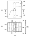
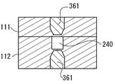
- FIG. 13 is a schematic view showing an example of the measuring device 100 according to the second embodiment
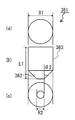
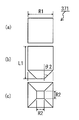
- FIG. 14 is a schematic enlarged view of a synthetic silica glass portion of the measuring device 100 of FIG.
- FIG. 13 (a) shows a schematic plan view (top view) of the measuring device as viewed from above, and FIG. 13 (b) shows a schematic cross section taken along line AA of FIG. 13 (a).
- 14A shows a top view of the synthetic silica glass chip 361
- FIG. 14B shows a side view
- FIG. 14C shows a bottom view.
- the measuring device 100 is formed by bonding a first flat plate 111 and a second flat plate 112.
- the first flat plate 111 and the second flat plate 112 are made of a plastic resin as in the first embodiment. Further, unlike the measurement device 100 according to the first embodiment, the measurement device 100 according to the second embodiment does not have a liquid feeding / merging portion.
- the measuring device 100 has a liquid inlet (inlet) 210 and an outlet (outlet) 245 on the surface.
- the liquid inlet 210 and the outlet 245 communicate with the flow path (channel) 240.
- the liquid inlet 210 and the outlet 245 have the same shape.
- the liquid inlet 210 and the outlet 245 are formed in the first flat plate 111. Further, the liquid introduction port 210 and the discharge port 245 communicate with a through hole extending in the thickness direction of the first flat plate 111. On the other hand, a recess of the flow path 240 is formed on the surface of the second flat plate 112 so as to communicate with each through hole. Further, the first flat plate 111 and the second flat plate 112 are bonded together to form the flow path 240.
- fitting holes 290 and 291 for fitting the synthetic silica glass part 360 (a pair of synthetic silica glass chips 361 having the same shape) to the first flat plate 111 and the second flat plate 112 are formed.
- the synthetic silica glass chip 361 is attached to the first flat plate 111 and the second flat plate 112 by being fitted into the fitting holes 290 and 291.
- the synthetic silica glass chip 361 fitted in the fitting hole 290 of the first flat plate 111 is disposed so as not to contact the second flat plate 112. For this reason, the whole bonding surface of the 2nd flat plate 112 is fixed to the bonding surface of the 1st flat plate 111 facing the said bonding surface.
- the synthetic silica glass chip 361 (Description of synthetic silica glass)
- the synthetic silica glass chip 361 has a shape in which a truncated inverted conical portion 362 and a cylindrical portion 363 are combined.
- the length L1 of the synthetic silica glass chip 361 is 0.875 mm
- the large diameter R1 is 1 mm
- the small diameter R2 of the surface constituting the boundary of the flow path 240 (see FIG. 13) is 0.2 mm.
- the small diameter R2 is set smaller than the width of the flow path 240 (see FIG. 13).
- the taper inclination ⁇ 2 of the truncated inverted conical portion 362 with respect to the axis of the synthetic silica glass chip 361 is, for example, 45 degrees.
- the upper surface and the lower surface of the synthetic silica glass chip 361 are formed as mirror surfaces.
- the upper surface and the lower surface of the synthetic silica glass chip 361 are a pair of opposing surfaces of the surfaces constituting the synthetic silica glass chip 361, and the synthetic silica glass chip 361 is incorporated in the microchannel device for measurement. When provided, it is a pair of surfaces consisting of a surface that becomes the incident surface of the measurement light and an opposing surface thereof.
- the arithmetic average roughness Ra of the mirror surface is less than 0.1 ⁇ m, preferably 0.05 ⁇ m or less.
- the side surface of the synthetic silica glass chip 361 is formed with a surface rougher than the mirror surface.
- the side surface formed of a rougher surface may be at least the side surface of the cylindrical portion 363, and may be both the side surface of the cylindrical portion 363 and the tapered surface of the truncated inverted conical portion 362.
- the arithmetic average roughness Ra of the rougher surface is, for example, from 0.1 ⁇ m to 1 ⁇ m, preferably from 0.2 m to 1 ⁇ m, and more preferably from 0.3 ⁇ m to 0.7 ⁇ m.
- FIG. 15 is a schematic diagram illustrating another example of the measurement device of FIG.
- FIG. 15A shows a schematic plan view (top view)
- FIG. 15B shows a schematic cross section taken along line AA of FIG. 15A.
- a third flat plate 113 may be provided between the first flat plate 111 and the second flat plate 112.
- the flow path 240 can be formed by forming a rectangular hole in the third flat plate 113, bonding one surface of the third flat plate to the first flat plate 111, and bonding the other surface to the second flat plate. . Since the depth of the flow path 240 is always the same as the thickness of the third flat plate 113 and the bottom surface of the flow path 240 is constituted by the surface of the second flat plate 112, the flow path 240 can be easily formed with high accuracy. it can.
- FIG. 16 is a schematic diagram showing still another example of the measurement device of FIG. FIG. 16 (a) shows a schematic plan view (top view), and FIG. 16 (b) shows a schematic cross section taken along line AA of FIG. 16 (a).
- the first flat plate 111 and the second flat plate 112 are each formed with a concave portion of the flow path 240, and the respective concave portions are combined to form one flow path space.
- the flow path 240 can be formed by bonding the 2nd flat plate 112 together.
- FIG. 17 are schematic cross-sectional views showing still other examples of the measuring device shown in FIG. 13 to FIG.
- the thickness of the first flat plate 111 or the second flat plate 112 may be provided between the synthetic silica glass chip 361 and the flow path 240 so as not to affect the measurement. In this case, even if a gap exists between the fitting hole and the synthetic silica glass chip 361, the gap and the flow path 240 do not communicate with each other. Therefore, it is possible to reliably avoid the leakage of the liquid in the flow path.
- synthetic silica glass chips having different shapes and / or sizes may be used for the first flat plate 111 and the second flat plate 112.
- the synthetic silica glass chip 364 fitted in the fitting hole of the second flat plate 112 is larger than the synthetic silica glass chip 361 fitted in the fitting hole of the first flat plate 111.
- the maximum diameter R31 of the synthetic silica glass chip 364 is larger than the maximum diameter R1 of the synthetic silica glass chip 361.
- at least the maximum diameter of the surface of the synthetic silica glass chip 361 on the channel 240 side is smaller than the width of the channel 240.
- the maximum diameter of the surface of the synthetic silica glass chip 364 on the channel 240 side may be smaller than the width of the channel 240.
- the pair of synthetic silica glass chips 381 and 382 may be cylindrical shapes having different sizes. That is, in FIG. 19, the maximum diameter R41 of the synthetic silica glass chip 382 is larger than the maximum diameter R1 of the synthetic silica glass chip 381. In FIG. 19, the maximum diameter (same as R1) of the surface on the flow path 240 side of the synthetic silica glass chip 381 on the upper side of the flow path is smaller than the width of the flow path 240, and the flow of the synthetic silica glass chip 382 is The maximum diameter of the surface on the side of the path 240 (same as R41) is larger than the width of the flow path 240.
- the present invention is not limited thereto, and the maximum diameter (same as R41) of the surface of the synthetic silica glass chip 382 on the flow channel 240 side may be smaller than the width of the flow channel 240, for example. Further, in at least one or both of the synthetic silica glass chips 381 and 382, the maximum diameter of the surface on the flow path 240 side may be the same as the width of the flow path 240.
- the pair of synthetic silica glass chips 371 may have a shape in which a truncated inverted quadrangular pyramid portion and a rectangular parallelepiped portion are combined.
- R1 is 1 mm
- R2 is 0.2 mm
- L1 is 1 mm.
- the slope ⁇ 2 of the inclined surface of the truncated inverted quadrangular pyramid with respect to the axis of the synthetic silica glass chip 371 is, for example, 45 degrees.
- FIG. 21 is a schematic diagram illustrating an example applicable to the measurement device 100 illustrated in FIGS. 13 to 20.
- three flow paths 240 of the measuring device 100 shown in FIGS. 13 to 20 may be arranged in parallel. In this case, the space for placing the measuring device 100 can be reduced and the throughput can be improved. In FIG. 21, three flow paths 240 are arranged in parallel. However, the present invention is not limited to this mode, and any other arbitrary number of flow paths 240 are arranged in parallel as appropriate by those skilled in the art in consideration of throughput. May be arranged.
- FIG. 22 is a schematic diagram illustrating an example applicable to the measurement device 100 illustrated in FIGS. 13 to 21.
- three fitting holes 290 for fitting three synthetic silica glass chips may be provided in one flow path 240 of the measuring device 100 shown in FIGS. .
- a silica glass chip 390 having a flow passage formed therethrough may be used.
- truncated inverted conical silica glass chips shown in FIGS. 2 and 3 instead of the truncated inverted quadrangular silica glass chips 301 a and 302 a may be used. Good.
- the material of the inorganic member is not particularly limited as long as it is a transparent inorganic material.
- a transparent inorganic oxide examples include oxides of elements selected from the group consisting of silicon, zinc, aluminum, titanium, zirconium, and indium.
- Specific examples of the transparent inorganic material include glass, sapphire, and diamond.
- the glass examples include silica glass, general glass, and optical glass. Silica glass includes synthetic and natural products.
- the measuring device of the present invention may use an organic member instead of the inorganic member.
- the organic material is an ultraviolet light transmissive transparent resin that transmits light having a wavelength of 450 nm or less, preferably 410 nm or less.
- a transparent resin transmits light having a wavelength of 220 nm or more and 450 nm or less, for example, 50% or more, preferably 80% or more.
- it is preferable that such transparent resin has little autofluorescence.
- a resin having no aromatic ring is preferable.
- examples of the ultraviolet transmissive transparent resin include an ultraviolet transmissive epoxy resin and an ultraviolet transmissive cyclic olefin resin.
- Examples of the ultraviolet light transmissive epoxy resin include a cured product of a resin composition containing an epoxy resin, a carboxylic acid anhydride curing agent, and a curing accelerator.
- the curing accelerator in this case is a tetraalkylphosphonium dialkyl phosphate represented by the following formula (I).
- R 1 , R 2 , R 3 , R 4 , R 5 and R 6 are alkyl groups or alkyl groups having a hydroxyl group. These alkyl groups have 1 to 8 carbon atoms.
- the alkyl group may be linear, branched or alicyclic.
- R 1 , R 2 , R 3 , R 4 , R 5 and R 6 may be the same group or different groups.
- content of the hardening accelerator represented by Formula (I) is 0.01 to 10 mass parts with respect to 100 mass parts of epoxy resins.
- the cyclic olefin resin examples include an injection molded product of a cyclic olefin resin composition containing a cyclic olefin resin and a low molecular weight cyclic olefin resin having a number average molecular weight of 10,000 or less.
- the cyclic olefin resin is a polyolefin resin containing a cyclic olefin component in the main chain.
- addition polymers of cyclic olefins and hydrogenated products thereof addition copolymers of cyclic olefins and ⁇ -olefins and hydrogenated products thereof, and ring opening of cyclic olefins, ring-opening copolymers of cyclic olefins and the like
- examples thereof include resins containing a cyclic olefin component as a copolymer component such as a hydrogenated product.
- the cyclic olefin resin composition in the above case contains 1 part by mass or more and 30 parts by mass or less of a low molecular weight cyclic olefin resin with respect to 100 parts by mass of the cyclic olefin resin.
- the injection-molded product has an ultraviolet irradiation wavelength of 544 nm and an autofluorescence intensity of 18000 or less at a fluorescence wavelength of 590 nm.
- the ultraviolet transmissive transparent resin a resin having desired characteristics is appropriately selected by those skilled in the art.
- a resin having desired characteristics is appropriately selected by those skilled in the art.
- it may be selected from an ultraviolet transparent acrylic resin and an ultraviolet transparent fluororesin.
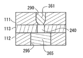
- Example of combination of inorganic and organic materials 26 is a schematic cross-sectional view showing still another example of the measuring device shown in FIG.
- a third flat plate 113 is provided between the first flat plate 111 and the second flat plate 112.
- a fitting hole 290 is formed in the first flat plate 111, and a synthetic silica glass chip 361 is fitted therein.
- a fitting hole 295 is formed in the second flat plate 112, and a cylindrical ultraviolet transmissive epoxy resin chip 365 is fitted therein.
- a rectangular hole is formed in the third flat plate 113, and the flow path 240 is formed by bonding one surface of the third flat plate to the first flat plate 111 and the other surface to the second flat plate.
- tip 361 can be provided as an incident window, and the ultraviolet-ray-transmissive epoxy resin chip
- tip 365 can be provided as a detection window, and each characteristic can be utilized.
- the inorganic member and the organic member in this manner, for example, on the incident side, the excellent light transmission property by the inorganic member is used, while on the detector side, the excellent surface modification diversity by the organic member is used. Thus, it becomes possible to use each characteristic in combination.
- the material of the resin member is not particularly limited and is appropriately selected by those skilled in the art.
- a transparent resin examples include polystyrene, polyethylene, polyvinyl chloride, polypropylene, polycarbonate, polyester, polymethyl methacrylate, polyvinyl acetate, vinyl-acetate copolymer, styrene-methyl methacrylate copolymer, and acrylonitrile-styrene copolymer.
- Acrylonitrile-butadiene-styrene copolymer nylon, polymethylpentene, silicone resin, amino resin, polysulfone, polyethersulfone, polyetherimide, fluororesin, and polyimide.
- the surface of the transparent member and the resin member on the flow path side may be appropriately subjected to surface modification treatment by those skilled in the art depending on the use of the analysis device, the analysis method, the characteristics of the liquid to be analyzed, and the like.
- the surface modification treatment can impart at least one of physical, chemical and biochemical characteristics. Specific examples include immobilization of physiologically active substances, immobilization of functional materials, introduction of functional groups, imparting hydrophilicity, imparting hydrophobicity, and the like.
- the measurement device 100 for optical analysis according to the present embodiment by using the silica glass portions 300, 310, 320, 330 and the synthetic silica glass portion 360 as a part of the detection site, Compared to the case where the entire measuring device 100 is formed of silica glass, the cost can be easily reduced.
- the measurement device 100 for optical analysis according to the present invention can be used as a cell sorter, a gene detection chip, a protein detection chip, or the like.
- the silica glass portions 300, 310, 320, 330 and the synthetic silica glass 360 are securely fitted into the fitting holes by the taper inclination of the silica glass portions 300, 310, 320, 330 and the synthetic silica glass portion 360.
- the gap between the first flat plate 111 and the second flat plate 112 and each silica glass chip and each synthetic silica glass chip can be made zero as much as possible, and leakage of liquid passing through the flow path 240 is prevented. be able to.
- the silica glass chips 301 and 302 and the synthetic silica glass chips 361, 364, 381, and 382 have a circular cross section, the pressure is uniformly applied to the circumferential side, so that the generation of gaps is prevented. The leakage of liquid passing through 240 can be reliably prevented.
- the silica glass chips 311, 312, 321, 322, 331, 332, and 371 have a rectangular cross section, it is easy to adjust the directionality with the flow path 240. As a result, the flow path 240 in the detection unit can be easily formed.
- the silica glass chip 341 and the silica glass chip 351 are integrally formed during the injection molding of the plastic resin member, the mass production of the measuring device 100 for optical analysis is realized at low cost. be able to. Further, since the silica glass chips 341 and 351 have the protrusions 346 and 356 for preventing the extraction from the plastic resin member forming the first flat plate 111 or the second flat plate 112, the first flat plate 111 or the second flat plate 112 is surely provided. Silica glass chips 341 and 351 can be attached to the substrate. As a result, the silica glass chips 341 and 351 can be prevented from being pulled out from the first flat plate 111 or the second flat plate 112.
- the arithmetic surface roughness Ra of the side surface portion of the cylindrical portion 363 is 0.1 ⁇ m or more and 1 ⁇ m or less. Can be prevented from being pulled out from. As a result, a stable measurement device for optical analysis can be formed.
- the first flat plate 111 and the second flat plate 112 correspond to a resin member
- the silica glass portions 300, 310, 320, 330 and the synthetic silica glass 360 correspond to an inorganic material member
- the flow path 240 flows.
- the measurement device 100 corresponds to a measurement device for optical analysis
- the taper slope ⁇ 1 corresponds to a taper portion
- a convex portion 346, 356 corresponds to a convex shape for preventing withdrawal
- the first flat plate 111 corresponds to a first resin member
- the second flat plate 112 corresponds to a second resin member.
- silica glass chip 301, synthetic silica glass chip 361 corresponds to the first inorganic member
- the silica glass chip 302 or the like corresponds to the second inorganic member.
Landscapes
- Chemical & Material Sciences (AREA)
- Health & Medical Sciences (AREA)
- General Health & Medical Sciences (AREA)
- Analytical Chemistry (AREA)
- Life Sciences & Earth Sciences (AREA)
- Biochemistry (AREA)
- Physics & Mathematics (AREA)
- General Physics & Mathematics (AREA)
- Immunology (AREA)
- Pathology (AREA)
- Dispersion Chemistry (AREA)
- Hematology (AREA)
- Clinical Laboratory Science (AREA)
- Chemical Kinetics & Catalysis (AREA)
- Optical Measuring Cells (AREA)
Description
本発明は、光学的分析用の測定デバイスに関する。より具体的には、本発明は、励起波長および検出波長として短波長の光線を利用する光学的分析用の測定デバイスに関する。特に、本発明は、マイクロ流路デバイスに関する。
従来から、短波長の光線を用いて細胞または遺伝子に関する測定が行われており、それらに使用する機器についても開発研究が進められている。例えば、日本国特開2010-181349号公報(特許文献1)には、従来のフローサイトメーターおよびセルソーターの有していたバイオハザード上の課題を解決する液体中微粒子解析装置について開示されている。
日本国特開2010-181349号公報(特許文献1)の液体中微粒子解析装置は、微粒子を含む試料液を流すための流路を備えたフローセルを載置する手段と、フローセルの流路を流れる試料液に光を照射する手段と、試料液中の該粒子から発生する散乱光および/または蛍光を検出するための光検出器と、光検出器で検出した信号の強度にもとづいて該粒子を解析する手段とを備える液体中微粒子解析装置において、フローセルは平板状基板に流路が形成されたものであって、流路側面に反射面が形成されており、その反射面はフローセルの流路内で発生した光のうち基板面内方向に進行する光をフローセル表面の特定領域に導き、光検出器は特定領域から外部に出てきた光を検出するものである。
日本国特開2010-181349号公報には、フローセルの平板状基板に反射面を形成することで側方の信号光を検出可能としたことが記載されている。しかしながら、当該フローセルは樹脂製であるため、短波長レーザーを透過しない。このため、短波長レーザーを用いた透過測定ができない点で問題となる。
一方、短波長の光線を用いた励起および透過測定を行うための光学的分析用測定デバイスの部材として最適なものの材質は、シリカガラス(石英ガラス)等である。したがって、光学的観点からは、光学的分析用測定デバイスの部材全てをシリカガラス等で製造することが好ましい。
しかしながら、石英ガラスは、樹脂に比べ非常に堅く軟化点もきわめて高い。したがって、とりわけマイクロ流路デバイスの平板状基板部材としては、石英ガラスは、高精度の流路を効率よく製造することが非常に困難である点、および、製造コストが増加する点で問題があった。
本発明の目的は、最適条件で測定でき、高精度でありながら比較的容易、かつ低コストで製造できる光学的分析用の測定デバイスを提供することである。
本発明の測定デバイスは、樹脂部材と、樹脂部材に取付けた450nm以下の波長の光を透過する透明部材と、樹脂部材を通って透明部材と接触しながら通過する流路と、を含むものである。
透明部材は、410nm以下の波長の光を透過するものであることがより好ましい。さらに、透明部材は無色透明であることが好ましい。
透明部材の素材としては、無機物および有機物を問わない。また、1つの測定デバイスの中で、透明部材として、無機物部材および有機物部材のいずれか一方が単独で用いられてもよいし、両方が組み合わされて用いられてもよい。無機物部材と有機物部材とが組み合わされる場合、組み合わせ態様の一例として、1つの検出部において、入射側と検出器側とでそれぞれ異なる素材を用いることができる。組み合わせ態様の他の一例として、1つの測定デバイスに複数の検出部を設け、検出部に応じて異なる素材を用いることもできる。
透明部材は、410nm以下の波長の光を透過するものであることがより好ましい。さらに、透明部材は無色透明であることが好ましい。
透明部材の素材としては、無機物および有機物を問わない。また、1つの測定デバイスの中で、透明部材として、無機物部材および有機物部材のいずれか一方が単独で用いられてもよいし、両方が組み合わされて用いられてもよい。無機物部材と有機物部材とが組み合わされる場合、組み合わせ態様の一例として、1つの検出部において、入射側と検出器側とでそれぞれ異なる素材を用いることができる。組み合わせ態様の他の一例として、1つの測定デバイスに複数の検出部を設け、検出部に応じて異なる素材を用いることもできる。
有機物である透明部材は、すなわち、透明樹脂部材である。透明樹脂部材は、220nm以上450nm以下の波長の光に対する透過率がたとえば50%以上、好ましくは80%以上である。
(1)
一局面に従う光学的分析用の測定デバイスは、樹脂部材と、樹脂部材に取付けた無機物部材と、樹脂部材を通って無機物部材と接触しながら通過する流路と、を含むものである。
一局面に従う光学的分析用の測定デバイスは、樹脂部材と、樹脂部材に取付けた無機物部材と、樹脂部材を通って無機物部材と接触しながら通過する流路と、を含むものである。
この場合、流路における検出領域の少なくとも一部に無機物部材を用いることで、流路全体を無機物部材で形成した場合と比較して、低コストでかつ容易に光学的分析用の測定デバイスを実現することが出来る。また、透過測定を確実に実施することができる。
一局面に従う光学的分析用の測定デバイスにおいて、樹脂部材は、平板状の樹脂基板であってよい。
無機物部材は、樹脂部材の一部に形成された嵌込孔または切欠部に嵌めこまれることによって取り付けられてよい。さらに、無機物部材と樹脂部材との組み合わせ形状が平板状となるように、無機部材が取り付けられることが好ましい。この場合、測定デバイスの外表面において、無機物部材と樹脂部材との境界における表面段差がないこと、または表面段差が0μm超100μm以下程度であることが好ましい。
無機物部材は、樹脂部材の一部に形成された嵌込孔または切欠部に嵌めこまれることによって取り付けられてよい。さらに、無機物部材と樹脂部材との組み合わせ形状が平板状となるように、無機部材が取り付けられることが好ましい。この場合、測定デバイスの外表面において、無機物部材と樹脂部材との境界における表面段差がないこと、または表面段差が0μm超100μm以下程度であることが好ましい。
樹脂部材には、流路が設けられている。樹脂部材における流路を構成する面の少なくともいずれかに、無機物部材の表面の少なくとも一部の面が連なることにより、双方の面が一体となって流路空間を規定してよい。以下において、流路空間を規定する無機部材の表面の少なくとも一部の面を、無機物部材の流路側表面と記載する。
無機物部材の表面には、凹部が形成されていてもよい。この場合、無機物部材における凹部表面は、樹脂部材における流路を構成する面の少なくともいずれかに連なることにより、当該流路を構成する面と一体となって流路空間を規定する。
無機物部材の表面には、凹部が形成されていてもよい。この場合、無機物部材における凹部表面は、樹脂部材における流路を構成する面の少なくともいずれかに連なることにより、当該流路を構成する面と一体となって流路空間を規定する。
無機物部材の流路側表面は、それに連なる樹脂部材の表面と面一(つまり段差が0μm)、または、当該樹脂部材の表面と0μm超100μm以下、好ましくは0μm超50μm以下の段差を有することを許容する。
樹脂部材表面と無機物部材表面との段差が上記範囲内であることにより、流路内は、樹脂部材と無機物部材との境界近傍であっても、液流が乱れにくい。したがって、液流が層流である場合も、層流状態を好ましく維持することができる。
樹脂部材表面と無機物部材表面との段差が上記範囲内であることにより、流路内は、樹脂部材と無機物部材との境界近傍であっても、液流が乱れにくい。したがって、液流が層流である場合も、層流状態を好ましく維持することができる。
無機物部材は、無機物部材の表面と樹脂部材の表面とがほぼ隙間なく接するように、樹脂部材に取り付けられていることが好ましい。すなわち、無機物部材を樹脂部材に嵌め込むための嵌め込み孔または切欠部は、無機物部材の形状に対応する形状となるように形成されることが好ましい。
(2)
第2の発明に係る光学的分析用の測定デバイスは、一局面に従う光学的分析用の測定デバイスにおいて、無機物部材は、テーパ部を有するものである。
第2の発明に係る光学的分析用の測定デバイスは、一局面に従う光学的分析用の測定デバイスにおいて、無機物部材は、テーパ部を有するものである。
この場合、無機物部材のテーパ部により樹脂部材に確実に無機物部材を嵌合わせ、一体に取付けることができる。特に、樹脂部材と無機物部材との隙間を限りなく零にすることができ、流路を通過する媒体の漏れを防止することができる。
第2の発明に係る光学的分析用の測定デバイスにおいて、テーパ部を有する無機物部材は、デバイスの厚み方向に軸心を有する形状であることが好ましい。テーパ部は、軸心に対して傾斜する傾斜面を有する。テーパ部を有する無機物部材は、たとえば切頭錐体の形状であってもよいし、柱体部と当該柱体部から軸方向に漸次先細に形成された切頭錐体部との組み合わせ形状であってもよい。
無機物部材において、軸心に対するテーパ部傾斜面の角度は、理論的には、0度超90度未満の範囲内である。
樹脂部材への嵌め込みやすさを考慮すると、無機物部材のテーパ部傾斜面の角度はある程度以上であることが好ましく、このような観点からは、当該傾斜面の角度はたとえば0度超90度未満であってよい。
また、樹脂部材への嵌め込み後の抜出防止を考慮すると、当該傾斜面の角度は小さい方が好ましい傾向にあり、このような観点からは、たとえば、0度超60度以下、好ましくは5度以上30度以下であってよい。
樹脂部材への嵌め込みやすさを考慮すると、無機物部材のテーパ部傾斜面の角度はある程度以上であることが好ましく、このような観点からは、当該傾斜面の角度はたとえば0度超90度未満であってよい。
また、樹脂部材への嵌め込み後の抜出防止を考慮すると、当該傾斜面の角度は小さい方が好ましい傾向にあり、このような観点からは、たとえば、0度超60度以下、好ましくは5度以上30度以下であってよい。
(3)
第3の発明に係る光学的分析用の測定デバイスは、一局面または第2の発明に係る光学的分析用の測定デバイスにおいて、無機物部材は、断面が円形である。
第3の発明に係る光学的分析用の測定デバイスは、一局面または第2の発明に係る光学的分析用の測定デバイスにおいて、無機物部材は、断面が円形である。
この場合、無機物部材が断面円形であるので、プラスチック樹脂部材に対して取付けやすい。特に、円周にテーパ部を有する場合、円周に圧力が均一にかかるので、隙間の発生を防止し、流路を通過する媒体の漏れを確実に防止することができる。
(4)
第4の発明に係る光学的分析用の測定デバイスは、一局面または第2の発明に係る光学的分析用の測定デバイスにおいて、無機物部材は、断面が矩形状である。
第4の発明に係る光学的分析用の測定デバイスは、一局面または第2の発明に係る光学的分析用の測定デバイスにおいて、無機物部材は、断面が矩形状である。
この場合、無機物部材が矩形状からなるので、流路の方向性を調整することが容易となる。その結果、樹脂部材と無機物部材との流路を確実に調整することができる。
(5)
第5の発明に係る光学的分析用の測定デバイスは、一局面から第4の発明のいずれかに係る光学的分析用の測定デバイスにおいて、無機物部材は、樹脂部材と一体成形されたものである。
第5の発明に係る光学的分析用の測定デバイスは、一局面から第4の発明のいずれかに係る光学的分析用の測定デバイスにおいて、無機物部材は、樹脂部材と一体成形されたものである。
この場合、樹脂部材の射出成形時に無機物部材の周囲を溶融樹脂が取り囲み、硬化することによって、樹脂が無機物部材と一体に成形される。このため、光学的分析用の測定デバイスの大量生産を安価に実現することができる。
(6)
第6の発明に係る光学的分析用の測定デバイスは、第5の発明に係る光学的分析用の測定デバイスにおいて、無機物部材は、樹脂部材から抜出防止の凸形状を有するものである。
第6の発明に係る光学的分析用の測定デバイスは、第5の発明に係る光学的分析用の測定デバイスにおいて、無機物部材は、樹脂部材から抜出防止の凸形状を有するものである。
この場合、無機物部材は、樹脂部材からの抜出防止のための凸形状部を有するので、確実に樹脂部材に無機物部材を取付けることができる。また、無機物部材が樹脂部材から抜出することを防止できるので、安定した光学的分析用の測定デバイスを形成することができる。
無機物部材における抜出防止のための凸形状部は、無機物部材の樹脂部材に接触する面から突出する形状であればよい。
(7)
第7の発明に係る光学的分析用の測定デバイスは、第5または第6の発明に係る光学的分析用の測定デバイスにおいて、無機物部材は、樹脂部材からの抜出防止のための算術平均粗さがRa0.1μm以上1μm以下の面を有するものである。
第7の発明に係る光学的分析用の測定デバイスは、第5または第6の発明に係る光学的分析用の測定デバイスにおいて、無機物部材は、樹脂部材からの抜出防止のための算術平均粗さがRa0.1μm以上1μm以下の面を有するものである。
つまり、無機物部材は、樹脂部材に接触する面が抜出防止面として形成されていることが好ましい。抜出防止面は、具体的には、0.1μm以上1μm以下、好ましくは、0.2μm以上1μm以下の算術平均粗さRaを有する。
抜出防止面には、無機物部材の抜出を防止するための表面加工がされていてよい。たとえば、抜出しを防止すべき方向(具体的には、無機物部材の軸体と平行な方向、または測定デバイスの厚み方向)と非平行に、筋目などの滑り止め模様が形成されてよい。
抜出防止面には、無機物部材の抜出を防止するための表面加工がされていてよい。たとえば、抜出しを防止すべき方向(具体的には、無機物部材の軸体と平行な方向、または測定デバイスの厚み方向)と非平行に、筋目などの滑り止め模様が形成されてよい。
この場合、無機物部材は、樹脂部材からの抜出防止のための算術平均粗さRaが0.1μm以上1μm以下の面を有するので、無機物部材が、樹脂部材から抜出することを防止できる。
なお、本明細書において、算術平均粗さRaは、JIS B 0601:2001に定められた規格に基づく。
なお、本明細書において、算術平均粗さRaは、JIS B 0601:2001に定められた規格に基づく。
(8)
第8の発明に係る光学的分析用の測定デバイスは、一局面から第7の発明のいずれかに係る光学的分析用の測定デバイスにおいて、樹脂部材は、第1樹脂部材および第2樹脂部材からなり、無機物部材は、第1樹脂部材に取付けられた第1無機物部材と、第2樹脂部材に取付けられた第2無機物部材とからなり、流路は、第1樹脂部材に形成された凹部と、第1無機物部材、第2樹脂部材および第2無機物部材の面とが組み合わせられることにより形成されたものである。
第8の発明に係る光学的分析用の測定デバイスは、一局面から第7の発明のいずれかに係る光学的分析用の測定デバイスにおいて、樹脂部材は、第1樹脂部材および第2樹脂部材からなり、無機物部材は、第1樹脂部材に取付けられた第1無機物部材と、第2樹脂部材に取付けられた第2無機物部材とからなり、流路は、第1樹脂部材に形成された凹部と、第1無機物部材、第2樹脂部材および第2無機物部材の面とが組み合わせられることにより形成されたものである。
この場合、第1無機物部材が取付けられた第1樹脂部材と、第2無機物部材が取付けられた第2樹脂部材とを張り合わせることで、容易に流路を形成することができる。好ましくは、流路の断面は矩形状である。
第2樹脂部材に取り付けられた無機物部材は、第1樹脂部材と接触しないように配設されることが好ましい。
無機物部材と樹脂部材との間の固定は、樹脂部材と樹脂部材との間の固定より弱い傾向にある。第2樹脂部材に取り付けられた無機物部材が、第1樹脂部材と接触しないように配設されることにより、検出部における流路の境界で相対的に弱い固定部分が生じることを回避することができる。このため、流路から液体の漏れを防止することができる。
無機物部材と樹脂部材との間の固定は、樹脂部材と樹脂部材との間の固定より弱い傾向にある。第2樹脂部材に取り付けられた無機物部材が、第1樹脂部材と接触しないように配設されることにより、検出部における流路の境界で相対的に弱い固定部分が生じることを回避することができる。このため、流路から液体の漏れを防止することができる。
なお、本発明の測定デバイスは、光学測定に使用する波長の光が短波長である場合に特に有用である。本発明における短波長とは、具体的には、450nm以下、好ましくは410nm以下の波長である。
本発明に係る光学的分析用の測定デバイスにおいて、無機物部材は、光学測定に使用する波長の光に対する透過率が例えば60%以上である。
なお、本発明において、上記の透過率は、アジレントテクノロジー株式会社製 UV-Vis-NIR 分光光度計 Cary 6000iで測定することにより得られる。
(9)
第9の発明に係る光学的分析用の測定デバイスは、一局面から第8の発明のいずれかに係る光学的分析用の測定デバイスにおいて、無機物部材は、光学的測定に使用する波長の光に対する透過率が80%以上であることがより好ましい。
第9の発明に係る光学的分析用の測定デバイスは、一局面から第8の発明のいずれかに係る光学的分析用の測定デバイスにおいて、無機物部材は、光学的測定に使用する波長の光に対する透過率が80%以上であることがより好ましい。
この場合、無機物部材は、光学的測定に使用する光の波長に対する透過率が80%以上であるので、透過測定を確実に実施することができる。
(10)
第10の発明に係る光学的分析用の測定デバイスは、一局面から第9の発明のいずれかに係る光学的分析用の測定デバイスにおいて、無機物部材は、シリカガラスである。
第10の発明に係る光学的分析用の測定デバイスは、一局面から第9の発明のいずれかに係る光学的分析用の測定デバイスにおいて、無機物部材は、シリカガラスである。
この場合、無機物部材は、シリカガラスであるので、透過測定を確実に実施することができる。
(11)
第11の発明に係る光学的分析用の測定デバイスは、一局面から第10の発明のいずれかに係る光学的分析用の測定デバイスにおいて、無機物部材は、180nm以上1000nm以下の波長の光を90%以上透過し、且つ1000nm以上2500nm以下の波長の光を80%以上透過する合成シリカガラスである。
第11の発明に係る光学的分析用の測定デバイスは、一局面から第10の発明のいずれかに係る光学的分析用の測定デバイスにおいて、無機物部材は、180nm以上1000nm以下の波長の光を90%以上透過し、且つ1000nm以上2500nm以下の波長の光を80%以上透過する合成シリカガラスである。
この場合、無機物部材は、180nm以上1000nm以下の波長の光を90%以上透過し、且つ1000nm以上2500nm以下の波長の光を80%以上透過する合成シリカガラスであるので、さらに透過測定を確実に実施することができる。
(12)
第12の発明に係る光学的分析用の測定デバイスは、一局面から第11の発明のいずれかに係る光学的分析用の測定デバイスにおいて、無機物部材は、平行な2つの鏡面を持ち、且つ鏡面の一方が流路と接すると共に鏡面の他方が外気と接している。
第12の発明に係る光学的分析用の測定デバイスは、一局面から第11の発明のいずれかに係る光学的分析用の測定デバイスにおいて、無機物部材は、平行な2つの鏡面を持ち、且つ鏡面の一方が流路と接すると共に鏡面の他方が外気と接している。
この場合、無機物部材は、平行な2つの鏡面を持ち、且つ鏡面の一方が流路と接すると共に鏡面の他方が外気と接しているので、透過測定を確実に実施することができる。
100 測定デバイス
111 第1平板
112 第2平板
300,310,320,330,360 シリカガラス部、合成シリカガラス部
220,240 流路
346,356 凸部
301,302,311,312,321,322,331,332,341,351,361,364,381,382,371,390,301a,302a シリカガラスチップ、合成シリカガラスチップ
111 第1平板
112 第2平板
300,310,320,330,360 シリカガラス部、合成シリカガラス部
220,240 流路
346,356 凸部
301,302,311,312,321,322,331,332,341,351,361,364,381,382,371,390,301a,302a シリカガラスチップ、合成シリカガラスチップ
以下、本発明に係る実施の形態において図面を用いて説明する。なお、以下、第1の実施の形態においては、無機物部材の一例としてシリカガラスを用いた場合について説明を行い、第2の実施の形態においては、無機物部材の一例として合成シリカガラスを用いた場合について説明を行う。
(第1の実施の形態)
図1は、第1の実施の形態に係る測定デバイス(マイクロ流路デバイス)の一例を示す模式図であり、図2および図3は図1の測定デバイスのシリカガラス部の模式的拡大図である。
図1は、第1の実施の形態に係る測定デバイス(マイクロ流路デバイス)の一例を示す模式図であり、図2および図3は図1の測定デバイスのシリカガラス部の模式的拡大図である。
図1(a)は測定デバイスを上から見た平面視を示し、図1(b)は図1(a)のA-A矢視断面を示す。図2(a)および図3(a)はシリカガラス部を構成するシリカガラスチップの上面視を示し、図2(b)および図3(b)はシリカガラスチップの側面視を示し、図2(c)および図3(c)はシリカガラスチップの底面(下面)視を示す。
なお、本発明において、シリカガラスチップの上面および下面とは、シリカガラスチップを構成する面のうちの対向する一対の面であって、かつ、シリカガラスチップがマイクロ流路デバイスに組み込まれ測定に供される場合に、測定光の入射面となる面およびその対向面からなる一対の面をいう。
なお、本発明において、シリカガラスチップの上面および下面とは、シリカガラスチップを構成する面のうちの対向する一対の面であって、かつ、シリカガラスチップがマイクロ流路デバイスに組み込まれ測定に供される場合に、測定光の入射面となる面およびその対向面からなる一対の面をいう。
(測定デバイスの構成)
図1に示すように、測定デバイス100は、第1平板111および第2平板112を張り合わせて形成される。第1平板111および第2平板112は、後述するシリカガラス部300を除いてプラスチック樹脂で構成される。
また、測定デバイス100は、主に送液合流部、検出部、および排出部の3つの領域を含む。
図1に示すように、測定デバイス100は、第1平板111および第2平板112を張り合わせて形成される。第1平板111および第2平板112は、後述するシリカガラス部300を除いてプラスチック樹脂で構成される。
また、測定デバイス100は、主に送液合流部、検出部、および排出部の3つの領域を含む。
測定デバイス100は、送液合流部の表面に、第1液導入口(インレット)210および第2液導入口(インレット)230を有する。第1液導入口210と第2液導入口230は、流路(チャンネル)220に連通し、流路220は、さらに流路240に連通する。
第1液導入口210および第2液導入口230は、第1平板111に形成される。第1液導入口210および第2液導入口230は、第1平板111の厚み方向に延在する貫通孔に通じる。一方、それぞれの貫通孔と連通し、かつ、第1液導入口210からの液流と第2液導入口230からの液流とが合流するデザインとなるように、流路220、240の凹部が第2平板112表面に溝状に形成される。さらに、第1平板111と第2平板112とが張り合わせられることにより、流路220、240が形成される。
なお、流路240は、検出部に近づくにつれて管路断面が小さくなるよう形成される。
なお、流路240は、検出部に近づくにつれて管路断面が小さくなるよう形成される。
測定デバイス100の検出部では、第1平板111および第2平板112に、シリカガラス部300を嵌合するための嵌合孔250,251が、流路240に連通するように形成されている。そして、当該嵌合孔250,251に、シリカガラス部300を構成するシリカガラスチップ301およびシリカガラスチップ302がそれぞれ嵌め込まれる。これにより、シリカガラスチップ301およびシリカガラスチップ302がそれぞれ第1平板111および第2平板112に取付けられる。
検出部の下流側の排出部では、第1平板111と第2平板112との両表面に、互いに対応する位置に凹部が形成されており、両凹部が流路240の一部を構成する。測定デバイス100の側面における流路240の終端は、排出口(アウトレット)245を構成する。
(シリカガラスチップ)
図2および図3を用いてシリカガラスチップの説明を行う。
図2に示すように、シリカガラスチップ301は、切頭逆円錐の形状を有する。シリカガラスチップ301の長さL1は1mmであり、小直径R2は0.2mmであり、シリカガラスチップ301の軸心方向(すなわち図2(b)の上下方向)に対する側面のテーパ傾斜θ1は、例えば30度である。
図2および図3を用いてシリカガラスチップの説明を行う。
図2に示すように、シリカガラスチップ301は、切頭逆円錐の形状を有する。シリカガラスチップ301の長さL1は1mmであり、小直径R2は0.2mmであり、シリカガラスチップ301の軸心方向(すなわち図2(b)の上下方向)に対する側面のテーパ傾斜θ1は、例えば30度である。
図3に示すように、シリカガラスチップ302は、切頭円錐形状の形状を有している。シリカガラスチップ302の長さL2は0.875mmであり、小直径R2は0.2mmであり、シリカガラスチップ302の軸心方向(すなわち図3(b)の上下方向)に対する側面のテーパ傾斜θ1は、例えば30度である。
シリカガラスチップ301,302の上下面は、測定光の照射を受ける。このため、当該上下面の算術平均粗さRaは、たとえば0.2μm以下、好ましくは0.1μm以下、さらに好ましくは0.05μm以下である。一方側面は、上下面より粗い表面で形成されている。より粗い表面で形成されている側面の算術平均粗さRaは、たとえば0.1μm以上1μm以下、好ましくは0.2μm以上1μm以下、さらに好ましくは、0.3μm以上0.7μm以下である。これにより、シリカガラスチップ301,302の、嵌合孔250,251からの抜出防止を図ることができる。
図2に示すシリカガラスチップ301は、第1平板111の嵌合孔250に圧入される。その結果、第1平板111は、嵌合孔250とシリカガラスチップ301との隙間が形成されず、かつ、シリカガラスチップ301の小直径面と第1平板111の表面との高低差が0μm以上50μm以下の範囲内となるように形成される。第1平板111の嵌合孔250とシリカガラスチップ301との隙間が形成されないことにより、流路240内の液体の漏れが発生しない。さらに、シリカガラスチップ301の小直径面と第1平板111の表面との高低差が0μm以上50μm以下の範囲内であることにより、流路240内の液流を層流として維持することができる。
同様に、図3に示すシリカガラスチップ302は、第2平板112の嵌合孔251に圧入される。その結果、第2平板112は、嵌合孔251とシリカガラスチップ302との隙間が形成されず、かつ、シリカガラスチップ302の小直径面と第2平板112の表面に形成された流路240の凹部底面との高低差が0μm以上50μm以下の範囲内となるように形成される。第2平板112の嵌合孔251とシリカガラスチップ302との隙間が形成されないことにより、流路240内の液体の漏れが発生しない。さらに、シリカガラスチップ302の小直径面と第2平板112の表面に形成された流路240の凹部底面との高低差が0μm以上50μm以下の範囲内であることにより、流路240内の液流を層流として維持することができる。
(測定デバイス中の液体の流れ)
第1液導入口210から導入された第1液が流路220を通過し、第2液導入口230から導入された第2液が別の流路220を通過する。流路220を通過した第1液の液流と第2液の液流とは、流路220と流路240との境界で合流し、流路240内で層流を形成する。
第1液導入口210から導入された第1液が流路220を通過し、第2液導入口230から導入された第2液が別の流路220を通過する。流路220を通過した第1液の液流と第2液の液流とは、流路220と流路240との境界で合流し、流路240内で層流を形成する。
続いて、第1液と第2液との層流は検出部に導かれ、層流状態を維持したままシリカガラス部300を通過し、光学的測定に供された後、排出部の排出口245から排出される。
(他の例)
続いて、第1の実施の形態にかかる測定デバイスの他の例について説明を行う。なお、第1の実施の形態において説明した部分と同じ部分については同符号を記載し、説明を省略する。
続いて、第1の実施の形態にかかる測定デバイスの他の例について説明を行う。なお、第1の実施の形態において説明した部分と同じ部分については同符号を記載し、説明を省略する。
図4は第1の実施の形態にかかる測定デバイスの他の例を示す模式図であり、図5および図6は図4の測定デバイスのシリカガラス部の模式的拡大図である。
図4(a)は測定デバイスを上から見た平面視(上面視)を示し、図4(b)は図4(a)のA-A矢視断面を示す。図5(a)および図6(a)はシリカガラスチップの上面視を示し、図5(b)および図6(b)ならびに図5(d)および図6(d)はシリカガラスチップの側面視を示し、図5(c)および図6(c)はシリカガラスチップの底面視を示す。
図4に示すように、測定デバイス100は、上面視で円形のシリカガラス部300の代わりに、上面視で四角形のシリカガラス部310を備える。
(シリカガラスチップ)
ここで、図5および図6を用いてシリカガラスチップの説明を行う。
図5に示すように、シリカガラスチップ311は、溝が設けられた六面体の形状を有する。当該六面体は、上面(図5(a)参照)と下面(図5(c)参照)とが大きさの異なる長方形で構成され、対向する2対の側面のうち一方の1対の側面が同形の台形(図5(b)参照)で構成され、他方の1対の側面が同形の長方形(図5(d)参照)で構成される。そして、シリカガラスチップ311の下面には、幅H3の溝が形成されている。これにより、他方の一対の側面の下部が幅H3の矩形状の切欠きを有する(図5(d)参照)。シリカガラスチップ311の長さL11は1mmであり、幅H1は4mmであり、幅H2は2mmである。また、溝幅H3は、0.19mmである。また、シリカガラスチップ311の軸心方向(すなわち図5(b)の上下方向)に対する側面のテーパ傾斜θ1は、例えば30度である。
ここで、図5および図6を用いてシリカガラスチップの説明を行う。
図5に示すように、シリカガラスチップ311は、溝が設けられた六面体の形状を有する。当該六面体は、上面(図5(a)参照)と下面(図5(c)参照)とが大きさの異なる長方形で構成され、対向する2対の側面のうち一方の1対の側面が同形の台形(図5(b)参照)で構成され、他方の1対の側面が同形の長方形(図5(d)参照)で構成される。そして、シリカガラスチップ311の下面には、幅H3の溝が形成されている。これにより、他方の一対の側面の下部が幅H3の矩形状の切欠きを有する(図5(d)参照)。シリカガラスチップ311の長さL11は1mmであり、幅H1は4mmであり、幅H2は2mmである。また、溝幅H3は、0.19mmである。また、シリカガラスチップ311の軸心方向(すなわち図5(b)の上下方向)に対する側面のテーパ傾斜θ1は、例えば30度である。
図6に示すように、シリカガラスチップ312は、六面体の形状を有する。当該六面体は、上面(図6(a)参照)と下面(図6(c)参照)とが大きさの異なる長方形で構成され、対向する2対の側面のうち一方の1対の側面が同形の台形(図6(b)参照)で構成され、他方の1対の側面が同形の長方形(図6(d)参照)で構成される。シリカガラスチップ312の長さL12は0.875mmであり、幅H2は2mmである。また、シリカガラスチップ312の軸心方向(すなわち図6(b)の上下方向)に対する側面のテーパ傾斜θ1は、例えば30度である。
図5に示すシリカガラスチップ311は、第1平板111の嵌合孔260に圧入される。その結果、第1平板111は、嵌合孔260とシリカガラスチップ311との隙間が形成されず、シリカガラスチップ311の下面と第1平板111の表面との高低差が0μm以上50μm以下の範囲内となるように形成される。第1平板111の嵌合孔260とシリカガラスチップ311との隙間が形成されないことにより、流路240内の液体の漏れが発生しない。さらに、シリカガラスチップ311の下面と第1平板111の表面との高低差が0μm以上50μm以下の範囲内であることにより、流路240内の液流を層流として維持することができる。
図6に示すシリカガラスチップ312は、第2平板112の嵌合孔261に圧入される。その結果、第2平板112は、嵌合孔261とシリカガラスチップ312との隙間が形成されず、かつ、シリカガラスチップ312の上面と第2平板112の表面に形成された流路240の凹部底面との高低差が0μm以上50μm以下の範囲内となるように形成される。第2平板112の嵌合孔261とシリカガラスチップ312との隙間が形成されないことにより、流路240内の液体の漏れが発生しない。さらに、シリカガラスチップ312の上面と第2平板112の表面に形成された流路240の凹部底面との高低差が0μm以上50μm以下の範囲内であることにより、流路240内の液流を層流として維持することができる。
なお、測定デバイス100において、第2平板112の嵌合孔261には、シリカガラスチップ312全体が圧入されているとともに、第1平板111との張り合わせによってシリカガラスチップ311の一部も圧入される。これにより、嵌合孔261内において、シリカガラスチップ312の上面とシリカガラスチップ311の下面とが当接する。
(さらに他の例)
続いて、第1の実施の形態にかかる測定デバイスのさらに他の例について説明を行う。なお、上記の実施の形態において説明した部分と同じ部分については同符号を記載し、説明を省略する。
続いて、第1の実施の形態にかかる測定デバイスのさらに他の例について説明を行う。なお、上記の実施の形態において説明した部分と同じ部分については同符号を記載し、説明を省略する。
図7は第1の実施の形態にかかる測定デバイスのさらに他の例を示す模式図であり、図8および図9は図7の測定デバイスのシリカガラス部の模式的拡大図である。
図7(a)は測定デバイスを上から見た平面視(上面視)を示し、図7(b)は図7(a)のA-A矢視断面を示す。図8(a)および図9(a)はシリカガラスチップの上面視を示し、図8(b)および図9(b)ならびに図8(d)および図8(d)はシリカガラスチップの側面視を示し、図8(c)および図9(c)はシリカガラスチップの底面視を示す。
図7に示すように、測定デバイス100は、上面視で円形のシリカガラス部300の代わりに、上面視で四角形のシリカガラス部320を備える。
(シリカガラスチップ)
ここで、図8および図9を用いてシリカガラスチップの説明を行う。
図8に示すように、シリカガラスチップ321は、溝が設けられた直方体の形状を有する。当該直方体は、下面に幅H3の溝が形成されている(図8(c)参照)。これにより、一対の側面の下部が幅H3の矩形状の切欠きを有する(図8(d)参照)。シリカガラスチップ321の長さL11は1mmであり、幅H1は4mmであり、幅H2は2mmであり、溝の幅H3は0.19mmである。
ここで、図8および図9を用いてシリカガラスチップの説明を行う。
図8に示すように、シリカガラスチップ321は、溝が設けられた直方体の形状を有する。当該直方体は、下面に幅H3の溝が形成されている(図8(c)参照)。これにより、一対の側面の下部が幅H3の矩形状の切欠きを有する(図8(d)参照)。シリカガラスチップ321の長さL11は1mmであり、幅H1は4mmであり、幅H2は2mmであり、溝の幅H3は0.19mmである。
同様に、図9に示すように、シリカガラスチップ322は、直方体の形状を有する。シリカガラスチップ322の長さL12は0.875mmである。
図8に示すシリカガラスチップ321は、第1平板111の嵌合孔270に圧入される。その結果、第1平板111は、嵌合孔270とシリカガラスチップ321との隙間が形成されず、シリカガラスチップ321の下面と第1平板111の表面との高低差が0μm以上50μm以下の範囲内となるように形成される。第1平板111の嵌合孔270とシリカガラスチップ321との隙間が形成されないことにより、流路240内の液体の漏れが発生しない。さらに、シリカガラスチップ321の下面と第1平板111の表面との高低差が0μm以上50μm以下の範囲内であることにより、流路240内の液流を層流として維持することができる。
図9に示すシリカガラスチップ322は、第2平板112の嵌合孔271に圧入される。その結果、第2平板112は、嵌合孔271とシリカガラスチップ322との隙間が形成されず、かつ、シリカガラスチップ322の上面と第2平板112の表面に形成された流路240の凹部底面との高低差が0μm以上50μm以下の範囲内となるように形成される。第2平板112の嵌合孔271とシリカガラスチップ322との隙間が形成されないことにより、流路240内の液体の漏れが発生しない。さらに、シリカガラスチップ322の上面と第2平板112の表面に形成された流路240の凹部底面との高低差が0μm以上50μm以下の範囲内であることにより、流路240内の液流を層流として維持することができる。
なお、測定デバイス100において、第2平板112の嵌合孔271には、シリカガラスチップ322全体が圧入されているとともに、第1平板111との張り合わせによってシリカガラスチップ321の一部も圧入される。これにより、嵌合孔271内において、シリカガラスチップ322の上面とシリカガラスチップ321の下面とが当接する。
(さらに他の例)
続いて、第1の実施の形態にかかる測定デバイスのさらに他の例について説明を行う。なお、上記の実施の形態において説明した部分と同じ部分については同符号を記載し、説明を省略する。
続いて、第1の実施の形態にかかる測定デバイスのさらに他の例について説明を行う。なお、上記の実施の形態において説明した部分と同じ部分については同符号を記載し、説明を省略する。
図10は測定デバイスのさらに他の例を示す模式図である。
図10に示すように、検出部の一部および排出部をシリカガラス部330で形成してもよい。
この場合、第1平板111の切欠部280に、流路240の凹部が形成されたシリカガラスチップ331を圧入し、第2平板112の切欠部281に、流路240の凹部が形成されたシリカガラスチップ332を圧入し、第1平板111と第2平板112とを貼り合わせて測定デバイス100を形成する。
図10に示すように、検出部の一部および排出部をシリカガラス部330で形成してもよい。
この場合、第1平板111の切欠部280に、流路240の凹部が形成されたシリカガラスチップ331を圧入し、第2平板112の切欠部281に、流路240の凹部が形成されたシリカガラスチップ332を圧入し、第1平板111と第2平板112とを貼り合わせて測定デバイス100を形成する。
(さらに他の例)
続いて、図11および図12は、測定デバイス100を形成する際のシリカガラス部のさらに他の例を示す模式的断面図である。
続いて、図11および図12は、測定デバイス100を形成する際のシリカガラス部のさらに他の例を示す模式的断面図である。
シリカガラスチップ341の形状は段付き円筒形であり、図11に示す断面形状を有する。図11は、シリカガラスチップ341の軸方向に平行な面で切断した場合の断面図である。当該段付き円筒は、異なる直径および異なる高さをそれぞれ有する3種の円筒部から構成される。具体的には、直径LF5、高さL8を有する円筒部、直径LF6、高さL9を有する円筒部、および直径LF7、高さL10を有する円筒部から構成される。なお、図11に示すシリカガラスチップ341の上面347および下面348は、レーザの照射を受ける。このため、上面347および下面348の表面粗さRaはたとえば0.2μm以下、好ましくは0.1μm以下、さらに好ましくは、0.05μm以下である。
シリカガラスチップ351の形状は、段付き円筒部と切頭逆円錐部とが組み合わされた形状であり、図12に示す断面形状を有する。図12は、シリカガラスチップ351の軸方向に平行な面で切断した場合の断面図である。当該段付き円筒部は、異なる直径および異なる高さをそれぞれ有する2種の円筒部から構成される。具体的には、直径LF6、高さL9を有する円筒部、および直径LF7、高さL10を有する円筒部から構成される。切頭逆円錐部は、小直径面の直径が直径LF5、大直径面の直径がLF6、高さがL8である。なお、図12に示すシリカガラスチップ351の上面357および下面358は、レーザの照射を受ける。このため、上面357および下面358の表面粗さRaはたとえば0.2μm以下、好ましくは0.1μm以下、さらに好ましくは、0.05μm以下である。
測定デバイスが図11に示すシリカガラスチップ341および/または図12に示すシリカガラスチップ351を含む場合、第1平板111および第2平板112は、それぞれ、インサート成形により、シリカガラスチップ341またはシリカガラスチップ351と樹脂とを一体に成形することにより製造する。
なお、第1平板111および第2平板112と、シリカガラスチップ341およびシリカガラスチップ351との組み合わせは、任意である。シリカガラスチップ341が第2平板112内に組み合わされる場合、図11に示す態様とは上下方向が逆となるように組み合わされる。つまり、面348は常に流路側に面するように位置する。シリカガラスチップ351についても同様である。
また、図11および図12に示すシリカガラスチップ341,351には、それぞれ、最も大きい直径LF6を有する円筒部の周囲が、凸部346,356を構成している。このため、インサート成形時において、凸部346,356の周囲に溶融樹脂が回りこむ。したがって、第1平板111および第2平板112において、凸部346,356は、シリカガラスチップ341,351の抜出防止の役割を果たす。また、図11および図12に示す面345,355は、面347,348,357,358と同じ観点で、算術平均粗さRaが0.2μm以下、好ましくは0.1μm以下、さらに好ましくは、0.05μm以下であってよい。
(第2の実施の形態)
以下、第2の実施の形態に係る測定デバイスの一例について説明を行う。なお、第1の実施の形態に係る測定デバイス100と同部材および同構造については、同一の符号を付し、説明を省略する。
以下、第2の実施の形態に係る測定デバイスの一例について説明を行う。なお、第1の実施の形態に係る測定デバイス100と同部材および同構造については、同一の符号を付し、説明を省略する。
第2の実施の形態に係る測定デバイスにおいては、シリカガラス部300の代わりに、合成シリカガラス部360を使用する。
図13は第2の実施の形態に係る測定デバイス100の一例を示す模式図であり、図14は、図13の測定デバイス100の合成シリカガラス部の模式的拡大図である。
図13(a)は測定デバイスを上から見た模式的平面視(上面視)を示し、図13(b)は図13(a)のA-A線の模式的断面を示す。図14(a)は合成シリカガラスチップ361の上面視を示し、図14(b)は側面視を示し、図14(c)は底面視を示す。
図13に示すように、測定デバイス100は、第1平板111および第2平板112を張り合わせて形成される。第1平板111および第2平板112は、第1の実施の形態と同様にプラスチック樹脂で構成される。
また、第1の実施の形態に係る測定デバイス100と異なり、第2の実施の形態に係る測定デバイス100は、送液合流部を有さない。
また、第1の実施の形態に係る測定デバイス100と異なり、第2の実施の形態に係る測定デバイス100は、送液合流部を有さない。
測定デバイス100は、表面に液導入口(インレット)210および排出口(アウトレット)245を有する。液導入口210および排出口245は、流路(チャンネル)240に連通する。液導入口210および排出口245は、同じ形状を有する。
液導入口210および排出口245は、第1平板111に形成される。さらに、液導入口210および排出口245は、第1平板111の厚み方向に延在する貫通孔に通じる。一方、それぞれの貫通孔と連通するように、流路240の凹部が第2平板112表面に形成される。さらに、第1平板111と第2平板112とが張り合わせられることにより、流路240が形成される。
測定デバイス100の検出部では、第1平板111および第2平板112に、合成シリカガラス部360(同一形状の一対の合成シリカガラスチップ361)を嵌合するための嵌合孔290,291が形成されている。そして、合成シリカガラスチップ361は、当該嵌合孔290,291に嵌合されることにより、第1平板111および第2平板112に取付けられる。
そして、第1平板111の嵌合孔290に嵌合された合成シリカガラスチップ361は、第2平板112と接触しないように配設される。このため、第2平板112の貼り合わせ面の全面が、当該貼り合わせ面と対向する第1平板111の貼り合わせ面に固定される。
(合成シリカガラスの説明)
ここで、図14を用いて合成シリカガラスチップ361の説明を行う。
図14に示すように、合成シリカガラスチップ361は、切頭逆円錐部362と円筒部363とが組み合わされた形状を有する。
合成シリカガラスチップ361の長さL1は0.875mmであり、大直径R1は1mmであり、流路240(図13参照)の境界を構成する面の小直径R2は0.2mmである。小直径R2は、流路240(図13参照)の幅よりも小さく設定される。合成シリカガラスチップ361の軸心に対する、切頭逆円錐部362のテーパ傾斜θ2は、例えば45度である。
ここで、図14を用いて合成シリカガラスチップ361の説明を行う。
図14に示すように、合成シリカガラスチップ361は、切頭逆円錐部362と円筒部363とが組み合わされた形状を有する。
合成シリカガラスチップ361の長さL1は0.875mmであり、大直径R1は1mmであり、流路240(図13参照)の境界を構成する面の小直径R2は0.2mmである。小直径R2は、流路240(図13参照)の幅よりも小さく設定される。合成シリカガラスチップ361の軸心に対する、切頭逆円錐部362のテーパ傾斜θ2は、例えば45度である。
また、合成シリカガラスチップ361の上面および下面は、鏡面で形成されている。合成シリカガラスチップ361の上面および下面とは、合成シリカガラスチップ361を構成する面のうちの対向する一対の面であって、かつ、合成シリカガラスチップ361がマイクロ流路デバイスに組み込まれ測定に供される場合に、測定光の入射面となる面およびその対向面からなる一対の面である。鏡面の算術平均粗さRaは、0.1μm未満、好ましくは、0.05μm以下である。
これに対して、合成シリカガラスチップ361の側面は、鏡面より粗い表面で形成されている。より粗い表面で形成されている側面は、少なくとも円筒部363の側面であればよく、円筒部363の側面と切頭逆円錐部362のテーパ面との両方であってもよい。より粗い表面の算術平均粗さRaは、たとえば0.1μm以上1μm以下、好ましくは0.2m以上1μm以下、さらに好ましくは0.3μm以上0.7μm以下である。これにより、合成シリカガラスチップ361の、嵌合孔290,291からの抜出防止を図ることができる。
これに対して、合成シリカガラスチップ361の側面は、鏡面より粗い表面で形成されている。より粗い表面で形成されている側面は、少なくとも円筒部363の側面であればよく、円筒部363の側面と切頭逆円錐部362のテーパ面との両方であってもよい。より粗い表面の算術平均粗さRaは、たとえば0.1μm以上1μm以下、好ましくは0.2m以上1μm以下、さらに好ましくは0.3μm以上0.7μm以下である。これにより、合成シリカガラスチップ361の、嵌合孔290,291からの抜出防止を図ることができる。
(他の例)
図15は、図13の測定デバイスの他の例を示す模式図である。図15(a)は模式的平面視(上面視)を示し、図15(b)は図15(a)のA-A線の模式的断面を示す。
図15は、図13の測定デバイスの他の例を示す模式図である。図15(a)は模式的平面視(上面視)を示し、図15(b)は図15(a)のA-A線の模式的断面を示す。
図15に示すように、第1平板111および第2平板112の間に、第3平板113を設けてもよい。この場合、第3平板113に矩形状の孔を形成し、第3平板の一方の面を第1平板111と張り合わせ、他方の面を第2平板と張り合わせることで、流路240を形成できる。流路240の深さが第3平板113の厚みと同じ常に一定であり、流路240の底面が第2平板112の表面によって構成されるため、流路240を精度よく容易に形成することができる。
(さらに他の例)
図16は、図13の測定デバイスのさらに他の例を示す模式図である。図16(a)は模式的平面視(上面視)を示し、図16(b)は図16(a)のA-A線の模式的断面を示す。
図16は、図13の測定デバイスのさらに他の例を示す模式図である。図16(a)は模式的平面視(上面視)を示し、図16(b)は図16(a)のA-A線の模式的断面を示す。
図16に示すように、第1平板111および第2平板112のいずれにも流路240の凹部を形成し、それぞれの凹部が合わさって一の流路空間を形成するように、第1平板111および第2平板112を貼り合わせることで、流路240を形成することができる。
(さらに他の例)
図17、図18、図19、図20は、図13から図16に示した測定デバイスのさらに他の例を示す模式的断面図である。
図17、図18、図19、図20は、図13から図16に示した測定デバイスのさらに他の例を示す模式的断面図である。
図17に示すように、合成シリカガラスチップ361と流路240との間に、第1平板111または第2平板112の肉が測定に影響の無い厚みで設けられてもよい。この場合、たとえ嵌合孔と合成シリカガラスチップ361との間に隙間が存在していたとしても、その隙間と流路240とが連通することがない。したがって、流路内の液体の漏れを確実に回避することができる。
また、図18に示すように、第1平板111と第2平板112とにおいて、異なる形状および/または大きさの合成シリカガラスチップが用いられてよい。図18では、第1平板111の嵌合孔に嵌合させた合成シリカガラスチップ361と比較して、第2平板112の嵌合孔に嵌合させた合成シリカガラスチップ364の方が大きい。具体的には、合成シリカガラスチップ361の最大径R1より、合成シリカガラスチップ364の最大径R31の方が大きい。また、少なくとも合成シリカガラスチップ361の流路240側の面の最大径は、流路240の幅よりも小さい。同様に、合成シリカガラスチップ364の流路240側の面の最大径も、流路240の幅よりも小さくてよい。
さらに、図19に示すように、一対の合成シリカガラスチップ381,382が大きさの異なる円筒状であってもよい。つまり、図19では、合成シリカガラスチップ381の最大径R1より、合成シリカガラスチップ382の最大径R41の方が大きい。なお、図19においては、流路の上側の合成シリカガラスチップ381の流路240側の面の最大径(R1と同じ)は、流路240の幅よりも小さく、合成シリカガラスチップ382の流路240側の面の最大径(R41と同じ)は、流路240の幅より大きい。
しかしながら、この態様に限定されず、たとえば、合成シリカガラスチップ382の流路240側の面の最大径(R41と同じ)も、流路240の幅より小さくてよい。また、合成シリカガラスチップ381,382の少なくとも一方または両方において、流路240側の面の最大径が流路240の幅と同じであってもよい。
しかしながら、この態様に限定されず、たとえば、合成シリカガラスチップ382の流路240側の面の最大径(R41と同じ)も、流路240の幅より小さくてよい。また、合成シリカガラスチップ381,382の少なくとも一方または両方において、流路240側の面の最大径が流路240の幅と同じであってもよい。
さらに、図20に示すように、一対の合成シリカガラスチップ371が、切頭逆四角錐部と直方体部とが組み合わされた形状を有してもよい。合成シリカガラスチップ371において、R1は1mm、R2は0.2mm、L1は1mmである。合成シリカガラスチップ371の軸心に対する切頭逆四角錐部の斜面の傾斜θ2は、例えば45度である。
(さらに他の例)
次いで、図21は、図13から図20に示した測定デバイス100に適用可能な例を示す模式図である。
次いで、図21は、図13から図20に示した測定デバイス100に適用可能な例を示す模式図である。
図21に示すように、図13から図20に示す測定デバイス100の流路240を3個並列に配設されるように構成されてもよい。この場合、測定デバイス100を載置するスペースを小さくし、スループット性を向上させることが出来る。なお、図21においては、流路240を3個並列配置することとしているが、この態様に限定されず、スループット性を考慮して当業者により適宜、他の任意の個数で流路240を並列配置させてよい。
(さらに他の例)
次いで、図22は、図13から図21に示した測定デバイス100に適用可能な例を示す模式図である。
次いで、図22は、図13から図21に示した測定デバイス100に適用可能な例を示す模式図である。
図22に示すように、図13から図21に示す測定デバイス100の1本の流路240に対して、3つの合成シリカガラスチップをそれぞれ嵌合させる嵌合孔290を3箇所設けてもよい。
この場合、同種の液体に対して同時に3回の測定を行うことが出来る。なお、図22においては、合成シリカガラスチップを嵌合する嵌合孔を3個直列配置する例を挙げたが、この態様に限定されず、他の任意の個数で合成シリカガラスチップを嵌合する嵌合孔を直列配置させてもよい。
また、図23に示すように、流路を貫通形成したシリカガラスチップ390を用いてもよい。
さらに、図24および図25に示すように、図2および図3に示した切頭逆円錐形状のシリカガラスチップの代わりに、切頭逆四角錐形状のシリカガラスチップ301a,302aを用いてもよい。
さらに、図24および図25に示すように、図2および図3に示した切頭逆円錐形状のシリカガラスチップの代わりに、切頭逆四角錐形状のシリカガラスチップ301a,302aを用いてもよい。
(無機物部材の材質)
無機物部材の材質は、透明の無機物であれば特に限定されない。たとえば、透明の無機酸化物が挙げられる。透明の無機酸化物としては、ケイ素、亜鉛、アルミニウム、チタン、ジルコニウム、インジウムからなる群から選ばれる元素の酸化物が挙げられる。透明の無機物の具体例としては、ガラス、サファイア、およびダイアモンドなどが挙げられる。ガラスとしては、シリカガラス、一般ガラス、および光学用ガラスなどが挙げられる。シリカガラスとしては、合成物および天然物を含む。
無機物部材の材質は、透明の無機物であれば特に限定されない。たとえば、透明の無機酸化物が挙げられる。透明の無機酸化物としては、ケイ素、亜鉛、アルミニウム、チタン、ジルコニウム、インジウムからなる群から選ばれる元素の酸化物が挙げられる。透明の無機物の具体例としては、ガラス、サファイア、およびダイアモンドなどが挙げられる。ガラスとしては、シリカガラス、一般ガラス、および光学用ガラスなどが挙げられる。シリカガラスとしては、合成物および天然物を含む。
(有機物部材の材質)
上述の実施形態では、無機物部材を用いた例を示したが、本発明の測定デバイスは、当該無機物部材の代わりに有機物部材を用いてもよい。
有機物部材は、450nm以下、好ましくは410nm以下の波長の光を透過する紫外線透過性透明樹脂である。このような透明樹脂は、220nm以上450nm以下の波長の光を、例えば50%以上、好ましくは80%以上透過するものである。また、このような透明樹脂は、自家蛍光が少ないものであることが好ましい。具体的には、芳香族環を有しない樹脂であることが好ましい。
上述の実施形態では、無機物部材を用いた例を示したが、本発明の測定デバイスは、当該無機物部材の代わりに有機物部材を用いてもよい。
有機物部材は、450nm以下、好ましくは410nm以下の波長の光を透過する紫外線透過性透明樹脂である。このような透明樹脂は、220nm以上450nm以下の波長の光を、例えば50%以上、好ましくは80%以上透過するものである。また、このような透明樹脂は、自家蛍光が少ないものであることが好ましい。具体的には、芳香族環を有しない樹脂であることが好ましい。
より具体的には、紫外線透過性透明樹脂として、紫外線透過性エポキシ樹脂、および紫外線透過性環状オレフィン樹脂が挙げられる。
紫外線透過性エポキシ樹脂としては、エポキシ樹脂、カルボン酸無水物硬化剤、及び硬化促進剤とを含む樹脂組成物の硬化物が挙げられる。この場合における硬化促進剤は、下記式(I)で表されるテトラアルキルホスホニウムジアルキルホスフェートである。

式(I)中、R1、R2、R3、R4、R5及びR6は、アルキル基又はヒドロキシル基を有するアルキル基である。これらアルキル基の炭素数は1以上8以下である。アルキル基は、直鎖状、分岐鎖状および脂環状を問わない。R1、R2、R3、R4、R5及びR6は、同一の基であっても異なる基であってもよい。
なお、式(I)で表される硬化促進剤の含有量は、エポキシ樹脂100質量部に対して0.01質量部以上10質量部以下である。
なお、式(I)で表される硬化促進剤の含有量は、エポキシ樹脂100質量部に対して0.01質量部以上10質量部以下である。
環状オレフィン系樹脂としては、環状オレフィン系樹脂と、数平均分子量が10000以下である低分子量環状オレフィン系樹脂とを含む環状オレフィン系樹脂組成物の射出成形物が挙げられる。この場合における環状オレフィン系樹脂は、環状オレフィン成分を主鎖に含むポリオレフィン系樹脂である。たとえば、環状オレフィンの付加重合体およびその水素添加物、環状オレフィンとα-オレフィンとの付加共重合体およびその水素添加物、ならびに、環状オレフィンの開環、環状オレフィンの開環共重合体およびその水素添加物など、環状オレフィン成分を共重合成分として含む樹脂が挙げられる。
なお、上記の場合の環状オレフィン系樹脂組成物は、環状オレフィン系樹脂100質量部に対して低分子量環状オレフィン系樹脂を1質量部以上30質量部以下含む。さらに、射出成形物は、紫外線の照射波長が544nm、蛍光波長590nmにおける自家蛍光強度が18000以下である。
上記の他にも、紫外線透過性透明樹脂としては、所望の特性を有する樹脂が当業者によって適宜選択される。たとえば、紫外線透過性アクリル樹脂および紫外線透過性フッ素樹脂などから選択されてもよい。
(無機物部材と有機物部材との組み合わせの例)
図26は、図15に示した測定デバイスのさらに他の例を示す模式的断面図である。図26の測定デバイスにおいては、第1平板111および第2平板112の間に、第3平板113が設けられる。
第1平板111には嵌合孔290が形成され、合成シリカガラスチップ361が嵌合させられている。第2平板112には嵌合孔295が形成され、円柱形状の紫外線透過性エポキシ樹脂チップ365が嵌合させられている。
第3平板113には矩形状の孔が形成され、第3平板の一方の面を第1平板111と張り合わせ、他方の面を第2平板と張り合わせることで、流路240が形成される。
図26は、図15に示した測定デバイスのさらに他の例を示す模式的断面図である。図26の測定デバイスにおいては、第1平板111および第2平板112の間に、第3平板113が設けられる。
第1平板111には嵌合孔290が形成され、合成シリカガラスチップ361が嵌合させられている。第2平板112には嵌合孔295が形成され、円柱形状の紫外線透過性エポキシ樹脂チップ365が嵌合させられている。
第3平板113には矩形状の孔が形成され、第3平板の一方の面を第1平板111と張り合わせ、他方の面を第2平板と張り合わせることで、流路240が形成される。
これによって、測定デバイスの検出部において、入射窓として合成シリカガラスチップ361、検出窓として紫外線透過性エポキシ樹脂チップ365を設けてそれぞれの特性を利用することができる。
このように無機物部材と有機物部材とを組み合わせることにより、たとえば、入射側では無機物部材による優れた光透過性を利用する一方、検出器側では有機物部材による優れた表面修飾多様性を利用する、というように、それぞれの特性を組み合わせて利用することが可能となる。
このように無機物部材と有機物部材とを組み合わせることにより、たとえば、入射側では無機物部材による優れた光透過性を利用する一方、検出器側では有機物部材による優れた表面修飾多様性を利用する、というように、それぞれの特性を組み合わせて利用することが可能となる。
(樹脂部材の材質)
樹脂部材の材質としては特に限定されず、当業者によって適宜選択される。好ましくは、透明樹脂である。樹脂部材の材質の例として、ポリスチレン、ポリエチレン、ポリ塩化ビニル、ポリプロピレン、ポリカーボネート、ポリエステル、ポリメチルメタクリレート、ポリビニルアセテート、ビニル-アセテート共重合体、スチレン-メチルメタクリレート共重合体、アクリロニトリル-スチレン共重合体、アクリロニトリル-ブタジエン-スチレン共重合体、ナイロン、ポリメチルペンテン、シリコン樹脂、アミノ樹脂、ポリスルフォン、ポリエーテルスルフォン、ポリエーテルイミド、フッ素樹脂、およびポリイミドなどが挙げられる。
樹脂部材の材質としては特に限定されず、当業者によって適宜選択される。好ましくは、透明樹脂である。樹脂部材の材質の例として、ポリスチレン、ポリエチレン、ポリ塩化ビニル、ポリプロピレン、ポリカーボネート、ポリエステル、ポリメチルメタクリレート、ポリビニルアセテート、ビニル-アセテート共重合体、スチレン-メチルメタクリレート共重合体、アクリロニトリル-スチレン共重合体、アクリロニトリル-ブタジエン-スチレン共重合体、ナイロン、ポリメチルペンテン、シリコン樹脂、アミノ樹脂、ポリスルフォン、ポリエーテルスルフォン、ポリエーテルイミド、フッ素樹脂、およびポリイミドなどが挙げられる。
(流路表面改質処理)
透明部材および樹脂部材の流路側表面には、分析デバイスの用途、分析方法、および分析に供する液体の特性などによって、当業者によって適宜表面改質処理が行われてよい。表面改質処理によって、物理的、化学的および生化学的の少なくともいずれかの特性を付与することができる。具体的には、生理活性物質の固定化、機能性材料の固定化、官能基の導入、親水性付与、および疎水性付与などが挙げられる。
透明部材および樹脂部材の流路側表面には、分析デバイスの用途、分析方法、および分析に供する液体の特性などによって、当業者によって適宜表面改質処理が行われてよい。表面改質処理によって、物理的、化学的および生化学的の少なくともいずれかの特性を付与することができる。具体的には、生理活性物質の固定化、機能性材料の固定化、官能基の導入、親水性付与、および疎水性付与などが挙げられる。
以上のように、本実施の形態に係る光学的分析用の測定デバイス100においては、検出部位の一部に、シリカガラス部300,310,320,330および合成シリカガラス部360を用いることで、測定デバイス100全体をシリカガラスで形成した場合と比較して、容易に低コスト化を図ることができる。
特に、本発明に係る光学的分析用の測定デバイス100は、セルソータ、遺伝子検出チップ、たんぱく質検出チップ等として利用することができる。
特に、本発明に係る光学的分析用の測定デバイス100は、セルソータ、遺伝子検出チップ、たんぱく質検出チップ等として利用することができる。
また、測定デバイス100において、シリカガラス部300,310,320,330および合成シリカガラス部360のテーパ傾斜により嵌合孔に確実にシリカガラス部300,310,320,330および合成シリカガラス360を嵌合わせ、一体に取付けることができる。特に、第1平板111および第2平板112と、各シリカガラスチップ、合成シリカガラスチップとのそれぞれとの隙間を限りなく零にすることができ、流路240を通過する液体の漏れを防止することができる。
また、シリカガラスチップ301,302,合成シリカガラスチップ361,364,381,382においては、断面が円形からなるので、円周側に圧力が均一にかかるので、隙間の発生を防止し、流路240を通過する液体の漏れを確実に防止することができる。また、シリカガラスチップ311,312,321,322,331,332,371においては、断面が矩形状であるので、流路240との方向性を調整することが容易となる。その結果、検出部における流路240を容易に形成することができる。
また、シリカガラスチップ341およびシリカガラスチップ351は、プラスチック樹脂部材の射出成形時にシリカガラスチップ341,351が一体に成形されるので、光学的分析用の測定デバイス100の大量生産を安価で実現することができる。また、シリカガラスチップ341,351は、第1平板111または第2平板112を形成するプラスチック樹脂部材から抜出防止の凸部346,356を有するので、確実に第1平板111または第2平板112にシリカガラスチップ341,351を取付けることができる。その結果、シリカガラスチップ341,351が第1平板111または第2平板112から抜出することを防止できる。
また、シリカガラスチップ301,302および合成シリカガラスチップ361においては、円筒状部363の側面部分の算術表面粗さRaが0.1μm以上1μm以下であるので、第1平板111および第2平板112から抜出することを防止できる。その結果、安定した光学的分析用の測定デバイスを形成することができる。
本実施の形態においては、第1平板111および第2平板112が樹脂部材に相当し、シリカガラス部300,310,320,330および合成シリカガラス360が無機物部材に相当し、流路240が流路に相当し、測定デバイス100が光学的分析用の測定デバイスに相当し、テーパ傾斜θ1がテーパ部に相当し、算術平均粗さがRa0.1μm以上1μm以下の面345,355、および凸部346,356が抜出防止の凸形状に相当し、第1平板111が第1樹脂部材に相当し、第2平板112が第2樹脂部材に相当し、例えばシリカガラスチップ301,合成シリカガラスチップ361が第1無機物部材に相当し、シリカガラスチップ302等が第2無機物部材に相当する。
本発明の好ましい実施の形態は上記の通りであるが、本発明はそれらだけに制限されない。本発明の精神と範囲から逸脱することのない様々な実施形態が他になされることは理解されよう。さらに、本実施形態において、本発明の構成による作用および効果を述べているが、これら作用および効果は、一例であり、本発明を限定するものではない。
Claims (12)
- 樹脂部材と、
前記樹脂部材に取付けた無機物部材と、
前記樹脂部材を通って前記無機物部材と接触しながら通過する流路と、を含むことを特徴とする光学的分析用の測定デバイス。 - 前記無機物部材は、テーパ部を有することを特徴とする請求項1記載の光学的分析用の測定デバイス。
- 前記無機物部材は、断面が円形からなることを特徴とする請求項1または2に記載の光学的分析用の測定デバイス。
- 前記無機物部材は、断面が矩形状からなることを特徴とする請求項1または2に記載の光学的分析用の測定デバイス。
- 前記無機物部材は、前記樹脂部材と一体成形されたことを特徴とする請求項1から4のいずれか1項に記載の光学的分析用の測定デバイス。
- 前記無機物部材は、前記樹脂部材から抜出防止の凸形状を有することを特徴とする請求項5記載の光学的分析用の測定デバイス。
- 前記無機物部材は、前記樹脂部材からの抜出防止のための算術平均粗さがRa0.1μmから1μmの面を有することを特徴とする請求項5または6に記載の光学的分析用の測定デバイス。
- 前記樹脂部材は、第1樹脂部材および第2樹脂部材からなり、前記無機物部材は、前記第1樹脂部材に取付けられた第1無機物部材と、前記第2樹脂部材に取付けられた第2無機物部材とからなり、
前記流路は、前記第1樹脂部材に形成された凹部と、前記第1無機物部材、前記第2樹脂部材および前記第2無機物部材の面とが組み合わせられることにより形成されたことを特徴とする請求項1から7のいずれか1項に記載の光学的分析用の測定デバイス。 - 前記無機物部材は、光学的測定に使用する光の波長に対する透過率が80%以上であることを特徴とする請求項1から8のいずれか1項に記載の光学的分析用の測定デバイス。
- 前記無機物部材は、シリカガラスであることを特徴とする請求項1から9のいずれか1項に記載の光学的分析用の測定デバイス。
- 前記無機物部材は、180nmから1000nmの波長の光を90%以上透過し、且つ1000nmから2500nmの波長の光を80%以上透過する合成シリカガラスであることを特徴とする請求項1から10のいずれか1項に記載の光学的分析用の測定デバイス。
- 前記無機物部材は、平行な2つの鏡面を持ち、且つ前記鏡面の一方が前記流路と接すると共に前記鏡面の他方が外気と接していることを特徴とする請求項1から11のいずれか1項に記載の光学的分析用の測定デバイス。
Priority Applications (1)
| Application Number | Priority Date | Filing Date | Title |
|---|---|---|---|
| JP2014519840A JP6251672B2 (ja) | 2012-06-05 | 2013-06-05 | 光学的分析用の測定デバイス |
Applications Claiming Priority (2)
| Application Number | Priority Date | Filing Date | Title |
|---|---|---|---|
| JP2012-127916 | 2012-06-05 | ||
| JP2012127916 | 2012-06-05 |
Publications (1)
| Publication Number | Publication Date |
|---|---|
| WO2013183290A1 true WO2013183290A1 (ja) | 2013-12-12 |
Family
ID=49711696
Family Applications (1)
| Application Number | Title | Priority Date | Filing Date |
|---|---|---|---|
| PCT/JP2013/003532 Ceased WO2013183290A1 (ja) | 2012-06-05 | 2013-06-05 | 光学的分析用の測定デバイス |
Country Status (2)
| Country | Link |
|---|---|
| JP (1) | JP6251672B2 (ja) |
| WO (1) | WO2013183290A1 (ja) |
Citations (3)
| Publication number | Priority date | Publication date | Assignee | Title |
|---|---|---|---|---|
| JP2001004532A (ja) * | 1999-06-18 | 2001-01-12 | Apurikusu:Kk | 光学分析用セル |
| JP2006084210A (ja) * | 2004-09-14 | 2006-03-30 | Mitsubishi Electric Corp | 分析装置 |
| JP2006133030A (ja) * | 2004-11-04 | 2006-05-25 | Apurikusu:Kk | 流体測定用光学セル及び光学分析計 |
Family Cites Families (2)
| Publication number | Priority date | Publication date | Assignee | Title |
|---|---|---|---|---|
| US7091035B2 (en) * | 2002-12-30 | 2006-08-15 | The United States Of America As Represented By The Department Of Health And Human Services | Cell culturing and storage systems, devices and methods |
| US7764374B2 (en) * | 2004-07-26 | 2010-07-27 | Serstech Ab | On-chip spectroscopy |
-
2013
- 2013-06-05 WO PCT/JP2013/003532 patent/WO2013183290A1/ja not_active Ceased
- 2013-06-05 JP JP2014519840A patent/JP6251672B2/ja not_active Expired - Fee Related
Patent Citations (3)
| Publication number | Priority date | Publication date | Assignee | Title |
|---|---|---|---|---|
| JP2001004532A (ja) * | 1999-06-18 | 2001-01-12 | Apurikusu:Kk | 光学分析用セル |
| JP2006084210A (ja) * | 2004-09-14 | 2006-03-30 | Mitsubishi Electric Corp | 分析装置 |
| JP2006133030A (ja) * | 2004-11-04 | 2006-05-25 | Apurikusu:Kk | 流体測定用光学セル及び光学分析計 |
Also Published As
| Publication number | Publication date |
|---|---|
| JPWO2013183290A1 (ja) | 2016-01-28 |
| JP6251672B2 (ja) | 2017-12-20 |
Similar Documents
| Publication | Publication Date | Title |
|---|---|---|
| CN101995398B (zh) | 光检测装置 | |
| CN102782502B (zh) | 微芯片和微粒分析装置 | |
| US7746466B2 (en) | System and method for flow cytometry | |
| US10583439B2 (en) | Hydrodynamic focusing apparatus and methods | |
| CN102272580B (zh) | 光信息解析装置及光信息解析方法 | |
| CN104111219A (zh) | 粒子分析装置及其制造方法 | |
| BRPI0808400A2 (pt) | Dispositivos atuadores de gotículas, configurações, e métodos para aperfeiçoar a detecção da absorbância. | |
| US20140370586A1 (en) | Microchip and microchip-type fine-particle measuring device | |
| US9063089B2 (en) | Optical measuring apparatus, flow cytometer, and optical measuring method | |
| WO2006092959A1 (ja) | マイクロ流路及びマイクロ流体チップ | |
| CN101581728A (zh) | 微芯片和用于微芯片的通道结构 | |
| JP4252545B2 (ja) | マイクロ流路及びマイクロ流体チップ | |
| US9921160B2 (en) | Multichannel analysis device | |
| EP3152546B1 (en) | Biased sample injection flow cell | |
| JP6251672B2 (ja) | 光学的分析用の測定デバイス | |
| US9079359B2 (en) | Microchip and method of manufacturing the same | |
| US11933716B2 (en) | Flow path plate, analysis apparatus, and analysis method | |
| US7586612B2 (en) | Photometric analysis of biological samples using in-plane detection | |
| JP4637610B2 (ja) | マイクロ流路及びマイクロチップ | |
| US12025546B2 (en) | Flow path device, method for manufacturing flow path device, flow path measuring device, and inspection apparatus | |
| US20150343437A1 (en) | Duct device | |
| JP2004361239A (ja) | マイクロ分析システム用光学系 | |
| JP5841328B2 (ja) | マイクロチップの製造方法およびマイクロチップ | |
| US10166543B2 (en) | Cell capturing cartridge | |
| JP6924452B2 (ja) | 光学測定システム及び光学セル |
Legal Events
| Date | Code | Title | Description |
|---|---|---|---|
| 121 | Ep: the epo has been informed by wipo that ep was designated in this application |
Ref document number: 13800793 Country of ref document: EP Kind code of ref document: A1 |
|
| ENP | Entry into the national phase |
Ref document number: 2014519840 Country of ref document: JP Kind code of ref document: A |
|
| NENP | Non-entry into the national phase |
Ref country code: DE |
|
| 122 | Ep: pct application non-entry in european phase |
Ref document number: 13800793 Country of ref document: EP Kind code of ref document: A1 |