WO2013171916A1 - Piezoelectric actuator, piezoelectric vibration device, and mobile terminal - Google Patents
Piezoelectric actuator, piezoelectric vibration device, and mobile terminal Download PDFInfo
- Publication number
- WO2013171916A1 WO2013171916A1 PCT/JP2012/072262 JP2012072262W WO2013171916A1 WO 2013171916 A1 WO2013171916 A1 WO 2013171916A1 JP 2012072262 W JP2012072262 W JP 2012072262W WO 2013171916 A1 WO2013171916 A1 WO 2013171916A1
- Authority
- WO
- WIPO (PCT)
- Prior art keywords
- piezoelectric actuator
- piezoelectric
- main surface
- electrode
- internal electrode
- Prior art date
Links
- 238000005304 joining Methods 0.000 claims description 22
- 239000000758 substrate Substances 0.000 claims description 20
- 239000004020 conductor Substances 0.000 claims description 12
- 210000000845 cartilage Anatomy 0.000 claims description 3
- 238000013459 approach Methods 0.000 claims description 2
- 239000000463 material Substances 0.000 description 23
- 238000005452 bending Methods 0.000 description 21
- 239000000853 adhesive Substances 0.000 description 15
- 230000001070 adhesive effect Effects 0.000 description 15
- 239000000919 ceramic Substances 0.000 description 14
- 238000000034 method Methods 0.000 description 10
- 229920005989 resin Polymers 0.000 description 9
- 239000011347 resin Substances 0.000 description 9
- 239000002245 particle Substances 0.000 description 6
- 239000011521 glass Substances 0.000 description 5
- 238000010030 laminating Methods 0.000 description 5
- 238000004519 manufacturing process Methods 0.000 description 5
- 239000011230 binding agent Substances 0.000 description 4
- 230000006866 deterioration Effects 0.000 description 4
- DOIRQSBPFJWKBE-UHFFFAOYSA-N dibutyl phthalate Chemical compound CCCCOC(=O)C1=CC=CC=C1C(=O)OCCCC DOIRQSBPFJWKBE-UHFFFAOYSA-N 0.000 description 4
- 239000004014 plasticizer Substances 0.000 description 4
- BQCADISMDOOEFD-UHFFFAOYSA-N Silver Chemical compound [Ag] BQCADISMDOOEFD-UHFFFAOYSA-N 0.000 description 3
- HFGPZNIAWCZYJU-UHFFFAOYSA-N lead zirconate titanate Chemical compound [O-2].[O-2].[O-2].[O-2].[O-2].[Ti+4].[Zr+4].[Pb+2] HFGPZNIAWCZYJU-UHFFFAOYSA-N 0.000 description 3
- 229910052451 lead zirconate titanate Inorganic materials 0.000 description 3
- 239000004745 nonwoven fabric Substances 0.000 description 3
- 238000007650 screen-printing Methods 0.000 description 3
- 229910052709 silver Inorganic materials 0.000 description 3
- 239000004332 silver Substances 0.000 description 3
- 239000004925 Acrylic resin Substances 0.000 description 2
- 229920000178 Acrylic resin Polymers 0.000 description 2
- RYGMFSIKBFXOCR-UHFFFAOYSA-N Copper Chemical compound [Cu] RYGMFSIKBFXOCR-UHFFFAOYSA-N 0.000 description 2
- MQIUGAXCHLFZKX-UHFFFAOYSA-N Di-n-octyl phthalate Natural products CCCCCCCCOC(=O)C1=CC=CC=C1C(=O)OCCCCCCCC MQIUGAXCHLFZKX-UHFFFAOYSA-N 0.000 description 2
- PXHVJJICTQNCMI-UHFFFAOYSA-N Nickel Chemical compound [Ni] PXHVJJICTQNCMI-UHFFFAOYSA-N 0.000 description 2
- 229910001252 Pd alloy Inorganic materials 0.000 description 2
- 239000004820 Pressure-sensitive adhesive Substances 0.000 description 2
- 230000002238 attenuated effect Effects 0.000 description 2
- BJQHLKABXJIVAM-UHFFFAOYSA-N bis(2-ethylhexyl) phthalate Chemical compound CCCCC(CC)COC(=O)C1=CC=CC=C1C(=O)OCC(CC)CCCC BJQHLKABXJIVAM-UHFFFAOYSA-N 0.000 description 2
- 239000002131 composite material Substances 0.000 description 2
- 229910052802 copper Inorganic materials 0.000 description 2
- 239000010949 copper Substances 0.000 description 2
- 238000006073 displacement reaction Methods 0.000 description 2
- 230000000694 effects Effects 0.000 description 2
- PCHJSUWPFVWCPO-UHFFFAOYSA-N gold Chemical compound [Au] PCHJSUWPFVWCPO-UHFFFAOYSA-N 0.000 description 2
- 229910052737 gold Inorganic materials 0.000 description 2
- 239000010931 gold Substances 0.000 description 2
- 238000000227 grinding Methods 0.000 description 2
- 229910052751 metal Inorganic materials 0.000 description 2
- 239000002184 metal Substances 0.000 description 2
- SWELZOZIOHGSPA-UHFFFAOYSA-N palladium silver Chemical compound [Pd].[Ag] SWELZOZIOHGSPA-UHFFFAOYSA-N 0.000 description 2
- 230000002093 peripheral effect Effects 0.000 description 2
- BASFCYQUMIYNBI-UHFFFAOYSA-N platinum Chemical compound [Pt] BASFCYQUMIYNBI-UHFFFAOYSA-N 0.000 description 2
- 239000000843 powder Substances 0.000 description 2
- 239000002002 slurry Substances 0.000 description 2
- 229910000679 solder Inorganic materials 0.000 description 2
- 229920005992 thermoplastic resin Polymers 0.000 description 2
- WSMQKESQZFQMFW-UHFFFAOYSA-N 5-methyl-pyrazole-3-carboxylic acid Chemical compound CC1=CC(C(O)=O)=NN1 WSMQKESQZFQMFW-UHFFFAOYSA-N 0.000 description 1
- ZTQSAGDEMFDKMZ-UHFFFAOYSA-N Butyraldehyde Chemical compound CCCC=O ZTQSAGDEMFDKMZ-UHFFFAOYSA-N 0.000 description 1
- 229910013641 LiNbO 3 Inorganic materials 0.000 description 1
- NIXOWILDQLNWCW-UHFFFAOYSA-N acrylic acid group Chemical group C(C=C)(=O)O NIXOWILDQLNWCW-UHFFFAOYSA-N 0.000 description 1
- 239000011248 coating agent Substances 0.000 description 1
- 238000000576 coating method Methods 0.000 description 1
- 238000004891 communication Methods 0.000 description 1
- 239000013078 crystal Substances 0.000 description 1
- 238000007606 doctor blade method Methods 0.000 description 1
- 210000004728 ear cartilage Anatomy 0.000 description 1
- 239000003822 epoxy resin Substances 0.000 description 1
- 238000010304 firing Methods 0.000 description 1
- 238000010438 heat treatment Methods 0.000 description 1
- 239000004973 liquid crystal related substance Substances 0.000 description 1
- GQYHUHYESMUTHG-UHFFFAOYSA-N lithium niobate Chemical compound [Li+].[O-][Nb](=O)=O GQYHUHYESMUTHG-UHFFFAOYSA-N 0.000 description 1
- 238000005259 measurement Methods 0.000 description 1
- 239000000203 mixture Substances 0.000 description 1
- 238000000465 moulding Methods 0.000 description 1
- 229910052759 nickel Inorganic materials 0.000 description 1
- 229920000620 organic polymer Polymers 0.000 description 1
- 239000000088 plastic resin Substances 0.000 description 1
- 238000007747 plating Methods 0.000 description 1
- 229910052697 platinum Inorganic materials 0.000 description 1
- 229920003229 poly(methyl methacrylate) Polymers 0.000 description 1
- 229920000647 polyepoxide Polymers 0.000 description 1
- 239000004926 polymethyl methacrylate Substances 0.000 description 1
- 229920005749 polyurethane resin Polymers 0.000 description 1
- 230000001902 propagating effect Effects 0.000 description 1
- 230000009257 reactivity Effects 0.000 description 1
- 238000005096 rolling process Methods 0.000 description 1
- 229920002050 silicone resin Polymers 0.000 description 1
- 239000002904 solvent Substances 0.000 description 1
- 229920003051 synthetic elastomer Polymers 0.000 description 1
- 229920003002 synthetic resin Polymers 0.000 description 1
- 239000000057 synthetic resin Substances 0.000 description 1
- 239000005061 synthetic rubber Substances 0.000 description 1
Images


Classifications
-
- H—ELECTRICITY
- H10—SEMICONDUCTOR DEVICES; ELECTRIC SOLID-STATE DEVICES NOT OTHERWISE PROVIDED FOR
- H10N—ELECTRIC SOLID-STATE DEVICES NOT OTHERWISE PROVIDED FOR
- H10N30/00—Piezoelectric or electrostrictive devices
- H10N30/20—Piezoelectric or electrostrictive devices with electrical input and mechanical output, e.g. functioning as actuators or vibrators
- H10N30/204—Piezoelectric or electrostrictive devices with electrical input and mechanical output, e.g. functioning as actuators or vibrators using bending displacement, e.g. unimorph, bimorph or multimorph cantilever or membrane benders
- H10N30/2047—Membrane type
-
- B—PERFORMING OPERATIONS; TRANSPORTING
- B06—GENERATING OR TRANSMITTING MECHANICAL VIBRATIONS IN GENERAL
- B06B—METHODS OR APPARATUS FOR GENERATING OR TRANSMITTING MECHANICAL VIBRATIONS OF INFRASONIC, SONIC, OR ULTRASONIC FREQUENCY, e.g. FOR PERFORMING MECHANICAL WORK IN GENERAL
- B06B1/00—Methods or apparatus for generating mechanical vibrations of infrasonic, sonic, or ultrasonic frequency
- B06B1/02—Methods or apparatus for generating mechanical vibrations of infrasonic, sonic, or ultrasonic frequency making use of electrical energy
- B06B1/06—Methods or apparatus for generating mechanical vibrations of infrasonic, sonic, or ultrasonic frequency making use of electrical energy operating with piezoelectric effect or with electrostriction
- B06B1/0603—Methods or apparatus for generating mechanical vibrations of infrasonic, sonic, or ultrasonic frequency making use of electrical energy operating with piezoelectric effect or with electrostriction using a piezoelectric bender, e.g. bimorph
-
- B—PERFORMING OPERATIONS; TRANSPORTING
- B06—GENERATING OR TRANSMITTING MECHANICAL VIBRATIONS IN GENERAL
- B06B—METHODS OR APPARATUS FOR GENERATING OR TRANSMITTING MECHANICAL VIBRATIONS OF INFRASONIC, SONIC, OR ULTRASONIC FREQUENCY, e.g. FOR PERFORMING MECHANICAL WORK IN GENERAL
- B06B1/00—Methods or apparatus for generating mechanical vibrations of infrasonic, sonic, or ultrasonic frequency
- B06B1/02—Methods or apparatus for generating mechanical vibrations of infrasonic, sonic, or ultrasonic frequency making use of electrical energy
- B06B1/06—Methods or apparatus for generating mechanical vibrations of infrasonic, sonic, or ultrasonic frequency making use of electrical energy operating with piezoelectric effect or with electrostriction
- B06B1/0607—Methods or apparatus for generating mechanical vibrations of infrasonic, sonic, or ultrasonic frequency making use of electrical energy operating with piezoelectric effect or with electrostriction using multiple elements
- B06B1/0611—Methods or apparatus for generating mechanical vibrations of infrasonic, sonic, or ultrasonic frequency making use of electrical energy operating with piezoelectric effect or with electrostriction using multiple elements in a pile
-
- H—ELECTRICITY
- H04—ELECTRIC COMMUNICATION TECHNIQUE
- H04M—TELEPHONIC COMMUNICATION
- H04M1/00—Substation equipment, e.g. for use by subscribers
- H04M1/02—Constructional features of telephone sets
-
- H—ELECTRICITY
- H04—ELECTRIC COMMUNICATION TECHNIQUE
- H04R—LOUDSPEAKERS, MICROPHONES, GRAMOPHONE PICK-UPS OR LIKE ACOUSTIC ELECTROMECHANICAL TRANSDUCERS; DEAF-AID SETS; PUBLIC ADDRESS SYSTEMS
- H04R17/00—Piezoelectric transducers; Electrostrictive transducers
-
- H—ELECTRICITY
- H04—ELECTRIC COMMUNICATION TECHNIQUE
- H04R—LOUDSPEAKERS, MICROPHONES, GRAMOPHONE PICK-UPS OR LIKE ACOUSTIC ELECTROMECHANICAL TRANSDUCERS; DEAF-AID SETS; PUBLIC ADDRESS SYSTEMS
- H04R31/00—Apparatus or processes specially adapted for the manufacture of transducers or diaphragms therefor
-
- H—ELECTRICITY
- H10—SEMICONDUCTOR DEVICES; ELECTRIC SOLID-STATE DEVICES NOT OTHERWISE PROVIDED FOR
- H10N—ELECTRIC SOLID-STATE DEVICES NOT OTHERWISE PROVIDED FOR
- H10N30/00—Piezoelectric or electrostrictive devices
- H10N30/20—Piezoelectric or electrostrictive devices with electrical input and mechanical output, e.g. functioning as actuators or vibrators
-
- H—ELECTRICITY
- H10—SEMICONDUCTOR DEVICES; ELECTRIC SOLID-STATE DEVICES NOT OTHERWISE PROVIDED FOR
- H10N—ELECTRIC SOLID-STATE DEVICES NOT OTHERWISE PROVIDED FOR
- H10N30/00—Piezoelectric or electrostrictive devices
- H10N30/50—Piezoelectric or electrostrictive devices having a stacked or multilayer structure
-
- H—ELECTRICITY
- H10—SEMICONDUCTOR DEVICES; ELECTRIC SOLID-STATE DEVICES NOT OTHERWISE PROVIDED FOR
- H10N—ELECTRIC SOLID-STATE DEVICES NOT OTHERWISE PROVIDED FOR
- H10N30/00—Piezoelectric or electrostrictive devices
- H10N30/80—Constructional details
- H10N30/85—Piezoelectric or electrostrictive active materials
- H10N30/853—Ceramic compositions
-
- H—ELECTRICITY
- H10—SEMICONDUCTOR DEVICES; ELECTRIC SOLID-STATE DEVICES NOT OTHERWISE PROVIDED FOR
- H10N—ELECTRIC SOLID-STATE DEVICES NOT OTHERWISE PROVIDED FOR
- H10N30/00—Piezoelectric or electrostrictive devices
- H10N30/80—Constructional details
- H10N30/87—Electrodes or interconnections, e.g. leads or terminals
- H10N30/871—Single-layered electrodes of multilayer piezoelectric or electrostrictive devices, e.g. internal electrodes
-
- H—ELECTRICITY
- H10—SEMICONDUCTOR DEVICES; ELECTRIC SOLID-STATE DEVICES NOT OTHERWISE PROVIDED FOR
- H10N—ELECTRIC SOLID-STATE DEVICES NOT OTHERWISE PROVIDED FOR
- H10N30/00—Piezoelectric or electrostrictive devices
- H10N30/80—Constructional details
- H10N30/87—Electrodes or interconnections, e.g. leads or terminals
- H10N30/872—Connection electrodes of multilayer piezoelectric or electrostrictive devices, e.g. external electrodes
-
- H—ELECTRICITY
- H10—SEMICONDUCTOR DEVICES; ELECTRIC SOLID-STATE DEVICES NOT OTHERWISE PROVIDED FOR
- H10N—ELECTRIC SOLID-STATE DEVICES NOT OTHERWISE PROVIDED FOR
- H10N30/00—Piezoelectric or electrostrictive devices
- H10N30/80—Constructional details
- H10N30/87—Electrodes or interconnections, e.g. leads or terminals
- H10N30/875—Further connection or lead arrangements, e.g. flexible wiring boards, terminal pins
-
- H—ELECTRICITY
- H04—ELECTRIC COMMUNICATION TECHNIQUE
- H04M—TELEPHONIC COMMUNICATION
- H04M1/00—Substation equipment, e.g. for use by subscribers
- H04M1/02—Constructional features of telephone sets
- H04M1/03—Constructional features of telephone transmitters or receivers, e.g. telephone hand-sets
-
- H—ELECTRICITY
- H04—ELECTRIC COMMUNICATION TECHNIQUE
- H04R—LOUDSPEAKERS, MICROPHONES, GRAMOPHONE PICK-UPS OR LIKE ACOUSTIC ELECTROMECHANICAL TRANSDUCERS; DEAF-AID SETS; PUBLIC ADDRESS SYSTEMS
- H04R2499/00—Aspects covered by H04R or H04S not otherwise provided for in their subgroups
- H04R2499/10—General applications
- H04R2499/11—Transducers incorporated or for use in hand-held devices, e.g. mobile phones, PDA's, camera's
Definitions
- the present invention relates to a piezoelectric vibration device, a piezoelectric actuator suitable for a mobile terminal, a piezoelectric vibration device, and a mobile terminal.
- the piezoelectric actuator as shown in FIG. 12 can generate a bending vibration in which the main surface is bent. Moreover, by applying to a piezoelectric vibration device, a portable terminal, etc., it can be set as the vibration source of these devices.
- the present invention has been devised in view of the above circumstances, and an object of the present invention is to provide a piezoelectric actuator, a piezoelectric vibration device, and a portable terminal that can obtain larger bending vibration.
- the piezoelectric actuator of the present invention includes a laminate in which an internal electrode and a piezoelectric layer are laminated, and a surface electrode electrically connected to the internal electrode on at least one main surface of the laminate,
- the laminated body includes an active portion in which the first pole and the second pole of the internal electrode overlap in the stacking direction, and an inactive portion other than the active portion, including a first pole and a second pole.
- the internal electrode arranged on the one main surface side is characterized in that an end portion located in the vicinity of the boundary between the active portion and the inactive portion is curved toward the other main surface side.
- the piezoelectric vibration device of the present invention includes the piezoelectric actuator and a vibration plate joined to the other main surface of the piezoelectric actuator.
- the portable terminal of the present invention includes the piezoelectric actuator, an electronic circuit, a display, and a housing, and the other main surface of the piezoelectric actuator is bonded to the display or the housing.
- the end portion of the internal electrode is curved, it becomes easy to draw out a force in the bending direction, so that it is possible to realize a piezoelectric actuator capable of performing a greater bending vibration.
- FIG. 3 is a schematic cross-sectional view taken along line BB shown in a).
- FIG. 2 is a schematic cross-sectional view taken along line CC shown in FIG. It is a schematic sectional drawing which shows the other example of FIG. It is a schematic sectional drawing which shows the other example of FIG. It is a schematic sectional drawing which shows the other example of FIG. It is a schematic sectional drawing which shows the other example of FIG. It is a schematic sectional drawing which shows the other example of FIG. It is a schematic sectional drawing which shows the other example of FIG. It is a schematic sectional drawing which shows the other example of FIG.
- FIG. 10 is a schematic cross-sectional view taken along line AA shown in FIG. 9.
- FIG. 10 is a schematic sectional view taken along line BB shown in FIG. 9.
- FIG. 6 is a schematic cross-sectional view taken along line -B.
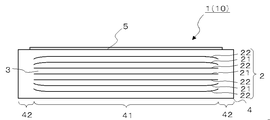
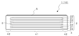
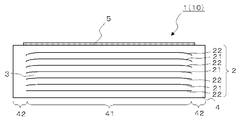
- FIG. 1A is a schematic perspective view showing an example of an embodiment of the piezoelectric actuator of the present invention
- FIG. 1B is a schematic cross-sectional view taken along the line AA shown in FIG.
- FIG. 1C is a schematic cross-sectional view taken along line BB shown in FIG.
- FIG. 2 is a schematic cross-sectional view taken along line CC shown in FIG.
- the piezoelectric actuator 1 of this embodiment shown in FIG. 1 includes a laminate 4 in which an internal electrode 2 and a piezoelectric layer 3 are laminated, and a surface electrically connected to the internal electrode 2 on at least one main surface of the laminate 4.
- the internal electrode 2 includes a first electrode 21 and a second electrode 22, and the stacked body 4 includes the first electrode 21 and the second electrode 22 of the internal electrode 2 that overlap in the stacking direction.
- the internal electrode 2 including the active part 41 and the inactive part 42 other than the active part 41 and disposed on the one main surface side has an end located near the boundary between the active part 41 and the inactive part 42 on the other main surface Curved to the side.
- the piezoelectric actuator 1 includes a piezoelectric element 10, and a laminated body 4 constituting the piezoelectric element 10 is formed by laminating an internal electrode 2 and a piezoelectric layer 3, and an active portion in which a plurality of internal electrodes 2 overlap in the laminating direction. 41 and other inactive portions 42 are formed, for example, in a long shape.
- the length of the laminate 4 is preferably, for example, 18 mm to 28 mm, and more preferably 22 mm to 25 mm.
- the width of the laminate 4 is preferably 1 mm to 6 mm, and more preferably 3 mm to 4 mm.
- the thickness of the laminate 4 is preferably 0.2 mm to 1.0 mm, and more preferably 0.4 mm to 0.8 mm.
- the internal electrode 2 constituting the laminated body 4 is formed by simultaneous firing with ceramics forming the piezoelectric layer 3 and includes a first electrode 21 and a second electrode 22.
- the first electrode 21 is a ground electrode
- the second electrode 22 is a positive electrode or a negative electrode.
- Piezoelectric layers 3 are alternately stacked to sandwich the piezoelectric layers 3 from above and below, and the first pole 21 and the second pole 22 are arranged in the stacking order, so that the piezoelectric body sandwiched between them.
- a driving voltage is applied to the layer 3.
- a conductor mainly composed of silver or a silver-palladium alloy having a low reactivity with piezoelectric ceramics, or a conductor containing copper, platinum, or the like can be used. You may make it contain.
- the end portions of the first pole 21 and the second pole 22 are alternately led to a pair of side surfaces facing each other of the stacked body 4.
- the length of the internal electrode 2 is preferably 17 mm to 25 mm, for example, and more preferably 21 mm to 24 mm.
- the width of the internal electrode 2 is preferably 1 mm to 5 mm, and more preferably 2 mm to 4 mm.
- the thickness of the internal electrode 2 is preferably 0.1 to 5 ⁇ m, for example.
- the piezoelectric layer 3 constituting the multilayer body 4 is formed of ceramics having piezoelectric characteristics.
- ceramics for example, a perovskite oxide made of lead zirconate titanate (PbZrO 3 -PbTiO 3 ), Lithium niobate (LiNbO 3 ), lithium tantalate (LiTaO 3 ), or the like can be used.
- the thickness of one layer of the piezoelectric layer 3 is preferably set to about 0.01 to 0.1 mm, for example, so as to be driven at a low voltage. In order to obtain a large bending vibration, it is preferable to have a piezoelectric d31 constant of 200 pm / V or more.
- a surface electrode 5 electrically connected to the internal electrode 2 is provided on at least one main surface of the laminate 4.
- the surface electrode 5 in the form shown in FIG. 1 includes a first surface electrode 51 having a large area, a second surface electrode 52 having a small area, and a third surface electrode 53.
- the first surface electrode 51 is electrically connected to the internal electrode 2 to be the first electrode 21, and the second surface electrode 52 is a second electrode disposed on one main surface side.
- the internal electrode 2 serving as the second electrode 22 and the third surface electrode 53 are electrically connected to the internal electrode 2 serving as the second electrode 22 disposed on the other main surface side.
- the length of the first surface electrode 51 is preferably, for example, 17 mm to 23 mm, and more preferably 19 mm to 21 mm.
- the width of the first surface electrode 51 is preferably 1 mm to 5 mm, for example, and more preferably 2 mm to 4 mm.
- the lengths of the second surface electrode 52 and the third surface electrode 53 are preferably 1 mm to 3 mm, for example.
- the widths of the second surface electrode 52 and the third surface electrode 53 are preferably 0.5 mm to 1.5 mm, for example.
- the piezoelectric actuator 1 shown in FIG. 1 is a so-called bimorph type piezoelectric actuator, and receives an electric signal from the surface electrode 5 and bends and vibrates so that one main surface and the other main surface are bent surfaces.
- the internal electrode 2 arranged on the one main surface side has an end portion located near the boundary between the active portion 41 and the inactive portion 42 curved toward the other main surface side. Yes.
- the piezoelectric actuator 1 can perform larger bending vibration with small electric power. Further, as a result of the effective use of energy by bending, it occurs at the boundary between the active part 41 and the inactive part 42 of the internal electrode close to one main surface (the boundary between the internal electrode 2 and the piezoelectric layer 3). The generation of microcracks can be reduced by reducing unnecessary stress, and deterioration of the piezoelectric actuator 1 due to deterioration can be suppressed.
- the degree of bending is such that the tangent at the end of the internal electrode 2 is inclined at 5 ° or more, particularly 10 ° or more with respect to the tangent drawn along the plane portion of the internal electrode 2. It is effective in that it is easy to draw out the force in the bending direction.
- the curved region is a range that is 10% or less of the total length of the internal electrode 2 from the end of the internal electrode 2 when viewed in cross section, and the crystal particles of the piezoelectric layer 3 in contact with the internal electrode 2 are present. This is a region where ten or more are in contact with each other from the end of the internal electrode 2.
- all the sides of the internal electrode 2 are curved, so that the stress relaxation effect is maximized, and the stress relaxation effect is further increased by curving both end portions of one side.
- FIG. 2 only the internal electrode 2 disposed on the one main surface side is curved toward the other main surface side, but the internal electrode 2 disposed on the other main surface side is also directed toward the one main surface side. It may be curved.
- end portions located in the vicinity of the boundary between the active portion 41 and the inactive portion 42 in the internal electrode 2 arranged on both main surface sides one main surface side and the other main surface side. In the case of the bimorph type, it becomes easy to draw out the force in the bending direction when bending to both main surface sides.
- the end portions of the internal electrode 2 located near the boundary between the active portion 41 and the inactive portion 42 may all be curved toward the other main surface side.
- the diaphragm is joined to the main surface, it is possible to more easily draw the force in the bending direction when bending.
- unnecessary stress generated at the boundary between the active part 41 and the inactive part 42 of the internal electrode is reduced to reduce the occurrence of microcracks, and the piezoelectric actuator 1 is deteriorated and the amount of displacement is reduced. Can be suppressed.
- the degree of curvature of the end portion of the internal electrode 2 increases as it approaches the one main surface.
- the internal electrode 2 closest to the other main surface of the laminate 4 may be flat, and the other main surface is bonded to an object to be subjected to vibration (such as a diaphragm described later).
- vibration such as a diaphragm described later.
- the surface electrode 5 (first surface electrode 51) is provided so as to extend in the width direction from the active portion 41 to the inactive portion 42. It is possible to make it easier to pull out the power.
- the surface electrode 5 and the internal electrode 2 so as to apply a voltage to the piezoelectric layer 3 positioned between the surface electrode 5 and the internal electrode 2 closest to the surface electrode 5, a region to which a voltage is applied can be obtained. Since the piezoelectric layer 3 sandwiched between the other internal electrodes 2 can be made wider in the width direction as well as in the longitudinal direction, a voltage is applied to the region of the inactive portion 42 to effectively bend it. This is because the displacement of can be induced. As a result, the stress generated at the boundary between the active part 41 and the inactive part 42 of the internal electrode 2 (the boundary between the internal electrode 2 and the piezoelectric layer 3) is reduced and the occurrence of microcracks is suppressed. Can do.
- the piezoelectric actuator 1 of the present invention includes a flexible substrate 6 having a wiring conductor 61, and the surface electrode 5 and the wiring conductor 61 are electrically connected via the conductive bonding member 7. As described above, a part of the flexible substrate 6 may be bonded to one main surface of the laminate 4.
- the flexible substrate 6 is, for example, a flexible printed wiring substrate in which two wiring conductors 61 are embedded in a resin film, and a connector (not shown) for connecting to an external circuit is connected to one end. .
- a conductive adhesive As the conductive bonding member 7, a conductive adhesive, solder, or the like is used, but a conductive adhesive is preferable.
- a conductive adhesive is used in which conductive particles 72 made of resin balls such as gold, copper, nickel, or gold plating are dispersed in a resin 71 such as an acrylic resin, an epoxy resin, a silicone resin, a polyurethane resin, or a synthetic rubber. This is because the stress caused by vibration can be reduced compared to solder.
- the conductive adhesive is preferably an anisotropic conductive material.
- the anisotropic conductive material is composed of conductive particles responsible for electrical bonding and a resin adhesive responsible for adhesion.
- connection part with 6 can be made compact.
- the piezoelectric actuator 1 shown in FIG. 1 is a so-called bimorph type piezoelectric actuator that receives an electric signal from the surface electrode 5 and vibrates and vibrates so that one main surface and the other main surface are bent surfaces.
- the piezoelectric actuator of the present invention is not limited to the bimorph type, and may be a unimorph type. For example, by joining (bonding) the other principal surface of the piezoelectric actuator to a diaphragm described later, It can be bent and vibrated.
- a ceramic green sheet to be the piezoelectric layer 3 is produced. Specifically, a ceramic slurry is prepared by mixing a calcined powder of piezoelectric ceramic, a binder made of an organic polymer such as acrylic or butyral, and a plasticizer. And a ceramic green sheet is produced using this ceramic slurry by using tape molding methods, such as a doctor blade method and a calender roll method.
- the piezoelectric ceramic any material having piezoelectric characteristics may be used.
- a perovskite oxide made of lead zirconate titanate (PbZrO 3 -PbTiO 3 ) can be used.
- the plasticizer dibutyl phthalate (DBP), dioctyl phthalate (DOP), or the like can be used.
- a conductive paste to be the internal electrode 2 is produced.
- a conductive paste is prepared by adding and mixing a binder and a plasticizer to a silver-palladium alloy metal powder. This conductive paste is applied on the ceramic green sheet in the pattern of the internal electrode 2 using a screen printing method. Further, a plurality of ceramic green sheets printed with this conductive paste are laminated, subjected to a binder removal treatment at a predetermined temperature, fired at a temperature of 900 to 1200 ° C., and then subjected to a predetermined grinding using a surface grinder or the like. By performing a grinding process so as to obtain a shape, a laminated body 4 including the internal electrodes 2 and the piezoelectric body layers 3 that are alternately laminated is manufactured.
- a mold or a resin mold having a dent is used as an upper mold (one main surface side) of the press device.
- a flat mold or resin mold as the lower mold (the other main surface side) of the press apparatus, the piezoelectric actuator 1 having the shape shown in FIG. 6 can be produced.
- the laminated body 4 is not limited to the one produced by the above manufacturing method, and any production is possible as long as the laminated body 4 formed by laminating a plurality of internal electrodes 2 and piezoelectric layers 3 can be produced. It may be produced by a method.
- a silver glass-containing conductive paste prepared by adding a binder, a plasticizer, and a solvent to a mixture of conductive particles mainly composed of silver and glass is used as a main electrode of the laminate 4 in the pattern of the surface electrode 5.
- a baking process is performed at a temperature of 650 to 750 ° C. to form the surface electrode 5.
- a via that penetrates the piezoelectric layer 3 may be formed or connected, or a side electrode may be formed on the side surface of the multilayer body 4. It may be produced by any manufacturing method.
- the flexible substrate 6 is connected and fixed (bonded) to the piezoelectric element 10 using the conductive bonding member 7.
- a conductive bonding member paste is applied and formed at a predetermined position of the piezoelectric element 10 using a technique such as screen printing. Then, the flexible substrate 6 is connected and fixed to the piezoelectric element 10 by curing the conductive bonding member paste in a state where the flexible substrate 6 is brought into contact therewith.
- the conductive bonding member paste may be applied and formed on the flexible substrate 6 side.
- the conductive bonding member 7 is a conductive adhesive
- the resin constituting the conductive adhesive is made of a thermoplastic resin
- the conductive adhesive is placed at a predetermined position on the piezoelectric element 10 or the flexible substrate 6.
- the thermoplastic resin softens and flows by heating and pressurizing the piezoelectric element 10 and the flexible substrate 6 in contact with a conductive adhesive.
- the plastic resin is cured, and the flexible substrate 6 is connected and fixed to the piezoelectric element 10.
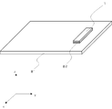
- the piezoelectric vibration device of the present invention has a piezoelectric actuator 1 and a vibration plate 81 attached to the other main surface of the piezoelectric actuator 1 as shown in FIG.
- the diaphragm 81 has a rectangular thin plate shape.
- the vibration plate 81 can be preferably formed using a material having high rigidity and elasticity such as acrylic resin or glass. Further, the thickness of the diaphragm 81 is set to 0.4 mm to 1.5 mm, for example.
- the diaphragm 81 is attached to the other main surface of the piezoelectric actuator 1 via a joining member 82.
- the entire surface of the other main surface may be bonded to the diaphragm 81 via the bonding member 82, or substantially the entire surface may be bonded.
- the joining member 82 has a film shape. Further, the joining member 82 is formed of a material that is softer and more easily deformed than the diaphragm 81, and has a smaller elastic modulus and rigidity such as Young's modulus, rigidity, and bulk modulus than the diaphragm 81. That is, the joining member 82 is deformable and deforms more greatly than the diaphragm 81 when the same force is applied. Then, the other main surface (main surface on the ⁇ z direction side in the drawing) of the piezoelectric actuator 1 is fixed to the one main surface (main surface on the + z direction side in the drawing) of the bonding member 82 as a whole. A part of one main surface (main surface on the + z direction side in the drawing) of the diaphragm 81 is fixed to the other main surface (main surface on the ⁇ z direction side in the drawing).
- the joining member 82 may be a single member or a composite composed of several members.
- a joining member 82 for example, a double-sided tape in which a pressure-sensitive adhesive is attached to both surfaces of a substrate made of a nonwoven fabric or the like, various elastic adhesives which are adhesives having elasticity, and the like can be suitably used.
- the thickness of the joining member 82 is desirably larger than the amplitude of the flexural vibration of the piezoelectric actuator 1, but if it is too thick, the vibration is attenuated, so it is set to 0.1 mm to 0.6 mm, for example.
- the material of the bonding member 82 is not limited, and the bonding member 82 may be formed of a material that is harder and less deformable than the vibration plate 81. In some cases, a configuration without the joining member 82 may be used.
- the piezoelectric vibration device of this example having such a configuration functions as a piezoelectric vibration device that causes the piezoelectric actuator 1 to bend and vibrate by applying an electric signal, thereby vibrating the vibration plate 81.
- the other end in the length direction of the diaphragm 81 (the end in the ⁇ y direction in the figure, the peripheral edge of the diaphragm 81, etc.) may be supported by a support member (not shown).
- the vibration plate 81 is joined to the other flat main surface of the piezoelectric actuator 1. Thereby, a piezoelectric vibration device in which the piezoelectric actuator 1 and the vibration plate 81 are firmly bonded can be obtained.
- the portable terminal of the present invention includes the piezoelectric actuator 1, an electronic circuit (not shown), a display 91, and a housing 92.
- the main surface is joined to the housing 92.
- 9 is a schematic perspective view schematically showing the portable terminal of the present invention
- FIG. 10 is a schematic cross-sectional view taken along line AA shown in FIG. 9
- FIG. 11 is a cross-sectional view taken along line BB shown in FIG. It is the schematic sectional drawing cut
- the piezoelectric actuator 1 and the housing 92 are joined using a deformable joining member. That is, in FIGS. 10 and 11, the joining member 82 is a deformable joining member.
- the deformable joining member 82 By joining the piezoelectric actuator 1 and the housing 92 with the deformable joining member 82, when the vibration is transmitted from the piezoelectric actuator 1, the deformable joining member 82 is deformed more greatly than the housing 92.
- the piezoelectric actuator 1 transmits strong vibration to the casing 92 without being influenced by the surrounding vibration. Can be made.
- the joining member 82 since at least a part of the joining member 82 is formed of a viscoelastic body, strong vibration from the piezoelectric actuator 1 is transmitted to the housing 92, while weak vibration reflected from the housing 92 is transmitted to the joining member 82. It is preferable in that it can be absorbed.
- a double-sided tape in which a pressure-sensitive adhesive is attached to both surfaces of a base material made of a nonwoven fabric or the like, or a joining member including an adhesive having elasticity can be used, and the thickness thereof is, for example, 10 ⁇ m to 2000 ⁇ m Can be used.
- the piezoelectric actuator 1 is attached to a part of the casing 92 that becomes the cover of the display 91, and a part of the casing 92 functions as the diaphragm 922.
- the piezoelectric actuator 1 is bonded to the housing 92, but the piezoelectric actuator 1 may be bonded to the display 91.
- the casing 92 includes a box-shaped casing main body 921 having one surface opened, and a diaphragm 922 that closes the opening of the casing main body 921.
- the casing 92 (the casing main body 921 and the diaphragm 922) can be preferably formed using a material such as a synthetic resin having high rigidity and elastic modulus.
- the peripheral edge of the diaphragm 922 is attached to the housing main body 921 via a bonding material 93 so as to vibrate.
- the bonding material 93 is formed of a material that is softer and easier to deform than the diaphragm 922, and has a smaller elastic modulus and rigidity such as Young's modulus, rigidity, and bulk modulus than the diaphragm 922. That is, the bonding material 93 can be deformed, and deforms more greatly than the diaphragm 922 when the same force is applied.
- the bonding material 93 may be a single material or a composite made up of several members.
- a bonding material 93 for example, a double-sided tape in which an adhesive is attached to both surfaces of a base material made of a nonwoven fabric or the like can be suitably used.
- the thickness of the bonding material 93 is set so that the vibration is not attenuated due to being too thick, and is set to, for example, 0.1 mm to 0.6 mm.
- the material of the bonding material 93 is not limited, and the bonding material 93 may be formed of a material that is harder and more difficult to deform than the diaphragm 922. In some cases, a configuration without the bonding material 93 may be used.
- Examples of the electronic circuit include a circuit that processes image information displayed on the display 91 and audio information transmitted by the mobile terminal, a communication circuit, and the like. At least one of these circuits may be included, or all the circuits may be included. Further, it may be a circuit having other functions. Furthermore, you may have a some electronic circuit.
- the electronic circuit and the piezoelectric actuator 1 are connected by a connection wiring (not shown).
- the display 91 is a display device having a function of displaying image information.
- a known display such as a liquid crystal display, a plasma display, and an organic EL display can be suitably used.
- the display 91 may have an input device such as a touch panel.
- the cover (diaphragm 922) of the display 91 may have an input device such as a touch panel.
- the entire display 91 or a part of the display 91 may function as a diaphragm.
- the portable terminal of the present invention is characterized in that the display 91 or the casing 92 generates vibration that transmits sound information through the ear cartilage or air conduction.
- the portable terminal of this example can transmit sound information by transmitting a vibration to the cartilage of the ear by bringing the diaphragm (display 91 or housing 92) into contact with the ear directly or via another object. That is, sound information can be transmitted by bringing a diaphragm (display 91 or housing 92) into direct or indirect contact with the ear and transmitting vibration to the cartilage of the ear.
- a portable terminal capable of transmitting sound information even when the surroundings are noisy can be obtained.
- the object interposed between the diaphragm (display 91 or housing 92) and the ear may be, for example, a cover of a mobile terminal, a headphone or an earphone, and any object that can transmit vibration. Anything can be used. Further, it may be a portable terminal that transmits sound information by propagating sound generated from the diaphragm (display 91 or housing 92) in the air. Furthermore, it may be a portable terminal that transmits sound information via a plurality of routes.
- the mobile terminal of this example transmits sound information using the piezoelectric actuator 1 that can effectively generate vibration, it can transmit high-quality sound information.
- a piezoelectric vibration device using the piezoelectric actuator shown in FIG. 6 was produced, and its characteristics were measured.
- the piezoelectric actuator had a long shape with a length of 23.5 mm, a width of 3.3 mm, and a thickness of 0.5 mm.
- the piezoelectric actuator has a structure in which piezoelectric layers having a thickness of 30 ⁇ m and internal electrodes are alternately stacked, and the total number of piezoelectric layers is 16.
- the piezoelectric layer was formed of lead zirconate titanate in which part of Zr was replaced with Sb.
- a resin mold having a dent is used as the mold on the upper side of the press device (the side in contact with one main surface).
- a piezoelectric actuator having a shape shown in FIG. 6 was produced using a flat mold as a lower mold (side contacting the other main surface) of the press apparatus.
- the surface electrode was printed so as to be longer by 1 mm in the width direction at both ends than the internal electrode.
- the amount of protrusion in the + z direction in the figure relative to both ends of the central portion on one main surface of the piezoelectric actuator was 10% (0.05 mm) of the thickness of the piezoelectric actuator.
- the other main surface of the piezoelectric actuator was almost flat.
- the other main surface of the piezoelectric actuator was stuck to the center of one surface of the glass plate with a double-sided tape, and 1 mm away from the other surface of the glass plate A microphone was installed at the position.
- Piezoelectric actuator 10 Piezoelectric element 2: Internal electrode 21: First pole 22: Second pole 3: Piezoelectric layer 4: Laminate 41: Active part 42: Inactive part 5: Surface electrode 51: First surface electrode 52: Second surface electrode 53: Third surface electrode 6: Flexible substrate 61: Wiring conductor 7: Conductive bonding member 71: Resin 72: Conductive particles 81: Diaphragm 82: Joining member 91: Display 92: Housing 921: Housing body 922: Diaphragm 93: Bonding material
Abstract
Description
10:圧電素子
2:内部電極
21:第1の極
22:第2の極
3:圧電体層
4:積層体
41:活性部
42:不活性部
5:表面電極
51:第1の表面電極
52:第2の表面電極
53:第3の表面電極
6:フレキシブル基板
61:配線導体
7:導電性接合部材
71:樹脂
72:導体粒子
81:振動板
82:接合部材
91:ディスプレイ
92:筐体
921:筐体本体
922:振動板
93:接合材 1: Piezoelectric actuator
10: Piezoelectric element 2: Internal electrode
21: First pole
22: Second pole 3: Piezoelectric layer 4: Laminate
41: Active part
42: Inactive part 5: Surface electrode
51: First surface electrode
52: Second surface electrode
53: Third surface electrode 6: Flexible substrate
61: Wiring conductor 7: Conductive bonding member
71: Resin
72: Conductive particles
81: Diaphragm
82: Joining member
91: Display
92: Housing
921: Housing body
922: Diaphragm
93: Bonding material
Claims (10)
- 内部電極および圧電体層が積層された積層体と、該積層体の少なくとも一方主面に前記内部電極と電気的に接続された表面電極とを備え、
前記内部電極は第1の極と第2の極とを含むとともに、前記積層体は前記内部電極の前記第1の極および前記第2の極が積層方向に重なる活性部と該活性部以外の不活性部とを含み、一方主面側に配置された内部電極は前記活性部と前記不活性部との境界近傍に位置する端部が他方主面側に向けて湾曲していることを特徴とする圧電アクチュエータ。 A laminated body in which an internal electrode and a piezoelectric layer are laminated, and a surface electrode electrically connected to the internal electrode on at least one main surface of the laminated body,
The internal electrode includes a first electrode and a second electrode, and the stacked body includes an active portion in which the first electrode and the second electrode of the internal electrode overlap each other in a stacking direction, and a portion other than the active portion. The internal electrode including the inactive portion and disposed on the one main surface side is characterized in that an end located near the boundary between the active portion and the inactive portion is curved toward the other main surface side. A piezoelectric actuator. - 前記一方主面側に配置された内部電極は前記一方主面に近づくにしたがって前記端部の湾曲の度合いが大きくなっていることを特徴とする請求項1に記載の圧電アクチュエータ。 2. The piezoelectric actuator according to claim 1, wherein the degree of curvature of the end portion of the internal electrode arranged on the one main surface side is increased as the one approaches the one main surface.
- 前記積層体の他方主面に最も近い内部電極は平坦であることを特徴とする請求項1または請求項2に記載の圧電アクチュエータ。 The piezoelectric actuator according to claim 1 or 2, wherein the internal electrode closest to the other main surface of the laminate is flat.
- 前記表面電極が前記活性部から前記不活性部にかけて設けられていることを特徴とする請求項1乃至請求項3のうちのいずれかに記載の圧電アクチュエータ。 The piezoelectric actuator according to any one of claims 1 to 3, wherein the surface electrode is provided from the active portion to the inactive portion.
- 配線導体を有するフレキシブル基板を備え、導電性接合部材を介して前記表面電極と前記配線導体とが電気的に接続されるように前記フレキシブル基板の一部が前記積層体の前記一方主面に接合されていることを特徴とする請求項1乃至請求項4のうちのいずれかに記載の圧電アクチュエータ。 A flexible substrate having a wiring conductor is provided, and a part of the flexible substrate is bonded to the one main surface of the laminate so that the surface electrode and the wiring conductor are electrically connected via a conductive bonding member. The piezoelectric actuator according to any one of claims 1 to 4, wherein the piezoelectric actuator is provided.
- 請求項1乃至請求項5のうちのいずれかに記載の圧電アクチュエータと、前記圧電素子の前記他方主面に接合された振動板とを有することを特徴とする圧電振動装置。 6. A piezoelectric vibration device comprising: the piezoelectric actuator according to claim 1; and a diaphragm bonded to the other main surface of the piezoelectric element.
- 前記圧電アクチュエータと前記振動板とが変形可能な接合部材を用いて接合されていることを特徴とする請求項6に記載の圧電振動装置。 The piezoelectric vibration device according to claim 6, wherein the piezoelectric actuator and the diaphragm are joined using a deformable joining member.
- 請求項1乃至請求項5のうちのいずれかに記載の圧電アクチュエータと、電子回路と、ディスプレイと、筐体とを有しており、
前記圧電アクチュエータの前記他方主面が前記ディスプレイまたは前記筐体に接合されていることを特徴とする携帯端末。 The piezoelectric actuator according to any one of claims 1 to 5, an electronic circuit, a display, and a housing,
The portable terminal, wherein the other main surface of the piezoelectric actuator is joined to the display or the casing. - 前記圧電アクチュエータと前記ディスプレイまたは前記筐体とが変形可能な接合部材を用いて接合されていることを特徴とする請求項8に記載の携帯端末。 9. The portable terminal according to claim 8, wherein the piezoelectric actuator and the display or the casing are joined using a deformable joining member.
- 前記ディスプレイまたは前記筐体は、耳の軟骨または気導を通して音情報を伝える振動を生じさせることを特徴とする請求項8または請求項9に記載の携帯端末。
The portable terminal according to claim 8 or 9, wherein the display or the casing generates vibration that transmits sound information through cartilage or air conduction of an ear.
Priority Applications (5)
| Application Number | Priority Date | Filing Date | Title |
|---|---|---|---|
| EP12876651.6A EP2854192B1 (en) | 2012-05-14 | 2012-08-31 | Piezoelectric actuator, piezoelectric vibration device, and mobile terminal |
| US14/372,251 US8994247B2 (en) | 2012-05-14 | 2012-08-31 | Piezoelectric actuator, piezoelectric vibration apparatus, and portable terminal |
| CN201280015223.4A CN103534828B (en) | 2012-05-14 | 2012-08-31 | Piezoelectric actuator, piezoelectric vibrating device and portable terminal |
| KR1020127025688A KR101601748B1 (en) | 2012-05-14 | 2012-08-31 | Piezoelectric actuator, piezoelectric vibration apparatus and portable terminal |
| JP2013516893A JP5537733B2 (en) | 2012-05-14 | 2012-08-31 | Piezoelectric actuator, piezoelectric vibration device, and portable terminal |
Applications Claiming Priority (2)
| Application Number | Priority Date | Filing Date | Title |
|---|---|---|---|
| JP2012111026 | 2012-05-14 | ||
| JP2012-111026 | 2012-05-14 |
Publications (1)
| Publication Number | Publication Date |
|---|---|
| WO2013171916A1 true WO2013171916A1 (en) | 2013-11-21 |
Family
ID=49583354
Family Applications (1)
| Application Number | Title | Priority Date | Filing Date |
|---|---|---|---|
| PCT/JP2012/072262 WO2013171916A1 (en) | 2012-05-14 | 2012-08-31 | Piezoelectric actuator, piezoelectric vibration device, and mobile terminal |
Country Status (7)
| Country | Link |
|---|---|
| US (1) | US8994247B2 (en) |
| EP (1) | EP2854192B1 (en) |
| JP (1) | JP5537733B2 (en) |
| KR (1) | KR101601748B1 (en) |
| CN (1) | CN103534828B (en) |
| TW (1) | TWI520389B (en) |
| WO (1) | WO2013171916A1 (en) |
Cited By (2)
| Publication number | Priority date | Publication date | Assignee | Title |
|---|---|---|---|---|
| JP2018152541A (en) * | 2017-02-13 | 2018-09-27 | Tdk株式会社 | Vibrating device |
| JP7425964B2 (en) | 2020-01-23 | 2024-02-01 | Tdk株式会社 | Piezoelectric element |
Families Citing this family (16)
| Publication number | Priority date | Publication date | Assignee | Title |
|---|---|---|---|---|
| CN104081791B (en) * | 2012-09-26 | 2017-03-08 | 京瓷株式会社 | Sound generator, sound generation device and electronic equipment |
| KR101878019B1 (en) | 2014-05-12 | 2018-07-13 | 파나소닉 아이피 매니지먼트 가부시키가이샤 | Method for connecting piezoelectric element with cable board, piezoelectric element affixed with cable board and inkjet head using the same |
| US10010909B2 (en) * | 2014-07-30 | 2018-07-03 | Kyocera Corporation | Piezoelectric element, acoustic generator, acoustic generation device, and electronic apparatus |
| DE102015216579A1 (en) * | 2015-08-31 | 2017-03-02 | Ziehl-Abegg Se | Fan, fan and system with at least one fan |
| JP6361640B2 (en) * | 2015-11-30 | 2018-07-25 | Tdk株式会社 | Piezoelectric element and piezoelectric actuator |
| JP1565481S (en) * | 2016-05-25 | 2016-12-19 | ||
| USD857020S1 (en) * | 2016-05-25 | 2019-08-20 | Tdk Corporation | Piezoelectric element |
| WO2018025617A1 (en) * | 2016-08-03 | 2018-02-08 | 株式会社村田製作所 | Deformation detection sensor, electronic device, and manufacturing method of deformation detection sensor |
| US10681172B2 (en) * | 2017-03-15 | 2020-06-09 | Sap Se | Secure data sharing through a network application |
| US11437560B2 (en) * | 2017-06-22 | 2022-09-06 | Taiyo Yuden Co., Ltd. | Multilayer piezoelectric element, piezoelectric vibration apparatus, and electronic device |
| US11296272B2 (en) * | 2017-07-20 | 2022-04-05 | Taiyo Yuden Co., Ltd. | Multilayer piezoelectric element, piezoelectric vibration apparatus, and electronic device |
| JP7163570B2 (en) * | 2017-09-20 | 2022-11-01 | Tdk株式会社 | Laminated piezoelectric element and vibration device |
| KR102605479B1 (en) | 2018-08-30 | 2023-11-22 | 엘지디스플레이 주식회사 | Piezoelectric element and display apparatus comprising the same |
| US10848875B2 (en) | 2018-11-30 | 2020-11-24 | Google Llc | Reinforced actuators for distributed mode loudspeakers |
| US10462574B1 (en) | 2018-11-30 | 2019-10-29 | Google Llc | Reinforced actuators for distributed mode loudspeakers |
| CN110351402B (en) * | 2019-06-28 | 2022-04-01 | 武汉华星光电技术有限公司 | Display module and mobile terminal |
Citations (10)
| Publication number | Priority date | Publication date | Assignee | Title |
|---|---|---|---|---|
| JPH0614396A (en) | 1991-11-30 | 1994-01-21 | Nippon Dempa Kogyo Co Ltd | Ultrasonic probe |
| JPH06291380A (en) * | 1993-03-31 | 1994-10-18 | Olympus Optical Co Ltd | Dielectric multilayered parts and its manufacture |
| JPH0745473A (en) * | 1993-05-24 | 1995-02-14 | Matsushita Electric Ind Co Ltd | Manufacture of multilayer ceramic capacitor |
| JP2002010393A (en) | 2000-04-19 | 2002-01-11 | Murata Mfg Co Ltd | Piezo-electric electroacoustic transducer |
| JP2002171002A (en) * | 2000-11-29 | 2002-06-14 | Kyocera Corp | Laminated piezoelectric element and injector |
| JP2003046154A (en) * | 2001-07-30 | 2003-02-14 | Ngk Insulators Ltd | Piezoelectric/electrostrictive element, piezoelectric/ electrostrictive device, and method of manufacturing them |
| WO2005004535A1 (en) | 2003-07-02 | 2005-01-13 | Citizen Electronics Co., Ltd. | Panel type speaker |
| JP2006238072A (en) | 2005-02-25 | 2006-09-07 | Nec Tokin Corp | Acoustic vibration generating piezoelectric bimorph element |
| JP2009177751A (en) * | 2008-01-28 | 2009-08-06 | Taiyo Yuden Co Ltd | Piezoelectric element, piezoelectrically vibrating plate and piezoelectric-type electroacoustic transducer |
| WO2012057214A1 (en) * | 2010-10-27 | 2012-05-03 | 京セラ株式会社 | Electronic equipment and mobile terminal provided with same |
Family Cites Families (11)
| Publication number | Priority date | Publication date | Assignee | Title |
|---|---|---|---|---|
| JP3249264B2 (en) | 1993-09-24 | 2002-01-21 | 株式会社トーキン | Manufacturing method of multilayer ceramic capacitor |
| JPH09270540A (en) * | 1996-03-29 | 1997-10-14 | Chichibu Onoda Cement Corp | Laminated piezoelectric actuator element and manufacturing method thereof |
| JP2000232027A (en) | 1999-02-10 | 2000-08-22 | Nippon Ceramic Co Ltd | Manufacture for laminated electronic components |
| US6653762B2 (en) | 2000-04-19 | 2003-11-25 | Murata Manufacturing Co., Ltd. | Piezoelectric type electric acoustic converter |
| JP2003023186A (en) | 2001-07-06 | 2003-01-24 | Nec Tokin Ceramics Corp | Multilayer piezoelectric actuator |
| CN101694865B (en) * | 2004-03-09 | 2013-03-20 | 京瓷株式会社 | Multilayer piezoelectric element and its manufacturing method |
| JP4782412B2 (en) * | 2004-12-24 | 2011-09-28 | 日本碍子株式会社 | Piezoelectric / electrostrictive body, piezoelectric / electrostrictive laminate, and piezoelectric / electrostrictive film type actuator |
| JP4736422B2 (en) * | 2004-12-24 | 2011-07-27 | 株式会社デンソー | Manufacturing method of multilayer piezoelectric element |
| JP5506009B2 (en) | 2007-02-27 | 2014-05-28 | キヤノン株式会社 | Piezoelectric element, method for manufacturing the same, diaphragm, and vibration wave drive device |
| JP5675137B2 (en) | 2010-03-23 | 2015-02-25 | キヤノン株式会社 | Piezoelectric element used in vibration device, vibration device, and dust removing device having vibration device |
| JP5558936B2 (en) * | 2010-06-29 | 2014-07-23 | 富士フイルム株式会社 | Method for manufacturing laminated element and laminated element |
-
2012
- 2012-08-31 WO PCT/JP2012/072262 patent/WO2013171916A1/en active Application Filing
- 2012-08-31 EP EP12876651.6A patent/EP2854192B1/en active Active
- 2012-08-31 JP JP2013516893A patent/JP5537733B2/en active Active
- 2012-08-31 CN CN201280015223.4A patent/CN103534828B/en active Active
- 2012-08-31 US US14/372,251 patent/US8994247B2/en active Active
- 2012-08-31 KR KR1020127025688A patent/KR101601748B1/en active IP Right Grant
-
2013
- 2013-05-14 TW TW102117073A patent/TWI520389B/en active
Patent Citations (10)
| Publication number | Priority date | Publication date | Assignee | Title |
|---|---|---|---|---|
| JPH0614396A (en) | 1991-11-30 | 1994-01-21 | Nippon Dempa Kogyo Co Ltd | Ultrasonic probe |
| JPH06291380A (en) * | 1993-03-31 | 1994-10-18 | Olympus Optical Co Ltd | Dielectric multilayered parts and its manufacture |
| JPH0745473A (en) * | 1993-05-24 | 1995-02-14 | Matsushita Electric Ind Co Ltd | Manufacture of multilayer ceramic capacitor |
| JP2002010393A (en) | 2000-04-19 | 2002-01-11 | Murata Mfg Co Ltd | Piezo-electric electroacoustic transducer |
| JP2002171002A (en) * | 2000-11-29 | 2002-06-14 | Kyocera Corp | Laminated piezoelectric element and injector |
| JP2003046154A (en) * | 2001-07-30 | 2003-02-14 | Ngk Insulators Ltd | Piezoelectric/electrostrictive element, piezoelectric/ electrostrictive device, and method of manufacturing them |
| WO2005004535A1 (en) | 2003-07-02 | 2005-01-13 | Citizen Electronics Co., Ltd. | Panel type speaker |
| JP2006238072A (en) | 2005-02-25 | 2006-09-07 | Nec Tokin Corp | Acoustic vibration generating piezoelectric bimorph element |
| JP2009177751A (en) * | 2008-01-28 | 2009-08-06 | Taiyo Yuden Co Ltd | Piezoelectric element, piezoelectrically vibrating plate and piezoelectric-type electroacoustic transducer |
| WO2012057214A1 (en) * | 2010-10-27 | 2012-05-03 | 京セラ株式会社 | Electronic equipment and mobile terminal provided with same |
Non-Patent Citations (1)
| Title |
|---|
| See also references of EP2854192A4 |
Cited By (2)
| Publication number | Priority date | Publication date | Assignee | Title |
|---|---|---|---|---|
| JP2018152541A (en) * | 2017-02-13 | 2018-09-27 | Tdk株式会社 | Vibrating device |
| JP7425964B2 (en) | 2020-01-23 | 2024-02-01 | Tdk株式会社 | Piezoelectric element |
Also Published As
| Publication number | Publication date |
|---|---|
| KR20140099564A (en) | 2014-08-13 |
| TW201401589A (en) | 2014-01-01 |
| EP2854192B1 (en) | 2018-03-07 |
| JPWO2013171916A1 (en) | 2016-01-07 |
| EP2854192A4 (en) | 2016-01-27 |
| CN103534828A (en) | 2014-01-22 |
| EP2854192A1 (en) | 2015-04-01 |
| KR101601748B1 (en) | 2016-03-09 |
| US8994247B2 (en) | 2015-03-31 |
| TWI520389B (en) | 2016-02-01 |
| CN103534828B (en) | 2015-09-16 |
| JP5537733B2 (en) | 2014-07-02 |
| US20150022058A1 (en) | 2015-01-22 |
Similar Documents
| Publication | Publication Date | Title |
|---|---|---|
| JP5537733B2 (en) | Piezoelectric actuator, piezoelectric vibration device, and portable terminal | |
| JP5474261B1 (en) | Piezoelectric actuator, piezoelectric vibration device, and portable terminal | |
| JP6140731B2 (en) | Piezoelectric actuator, piezoelectric vibration device, and portable terminal | |
| JP5902831B2 (en) | Piezoelectric actuator, piezoelectric vibration device, and portable terminal | |
| JP5788110B2 (en) | Piezoelectric element and piezoelectric vibration device including the same, portable terminal, acoustic generator, acoustic generator, and electronic device | |
| JP5566533B2 (en) | Piezoelectric actuator, piezoelectric vibration device, and portable terminal | |
| JP5474262B1 (en) | Piezoelectric actuator, piezoelectric vibration device, and portable terminal | |
| JP2015126605A (en) | Piezoelectric actuator, piezoelectric vibration device having the same, portable terminal, acoustic generator, and electronic apparatus | |
| JP5865963B2 (en) | Piezoelectric actuator, piezoelectric vibration device, and portable terminal | |
| WO2013171918A1 (en) | Piezoelectric actuator, piezoelectric vibration device, and mobile terminal | |
| JP6741609B2 (en) | Piezoelectric actuator, piezoelectric vibration device, and electronic device | |
| WO2014050240A1 (en) | Piezoelectric actuator, piezoelectric oscillation device and portable terminal | |
| JP6193748B2 (en) | Piezoelectric actuator, piezoelectric vibration device including the same, portable terminal, acoustic generator, electronic device |
Legal Events
| Date | Code | Title | Description |
|---|---|---|---|
| ENP | Entry into the national phase |
Ref document number: 20127025688 Country of ref document: KR Kind code of ref document: A |
|
| ENP | Entry into the national phase |
Ref document number: 2013516893 Country of ref document: JP Kind code of ref document: A |
|
| 121 | Ep: the epo has been informed by wipo that ep was designated in this application |
Ref document number: 12876651 Country of ref document: EP Kind code of ref document: A1 |
|
| WWE | Wipo information: entry into national phase |
Ref document number: 2012876651 Country of ref document: EP |
|
| WWE | Wipo information: entry into national phase |
Ref document number: 14372251 Country of ref document: US |
|
| NENP | Non-entry into the national phase |
Ref country code: DE |