WO2013162148A1 - Compound for organic optoelectric device, organic light emitting device containing same, and display device containing said organic light emitting device - Google Patents
Compound for organic optoelectric device, organic light emitting device containing same, and display device containing said organic light emitting device Download PDFInfo
- Publication number
- WO2013162148A1 WO2013162148A1 PCT/KR2012/011061 KR2012011061W WO2013162148A1 WO 2013162148 A1 WO2013162148 A1 WO 2013162148A1 KR 2012011061 W KR2012011061 W KR 2012011061W WO 2013162148 A1 WO2013162148 A1 WO 2013162148A1
- Authority
- WO
- WIPO (PCT)
- Prior art keywords
- formula
- substituted
- unsubstituted
- group
- compound
- Prior art date
Links
- 0 C(C1C2C34c5ccccc5C5C=CC=CC35)C1C=CC2c(cc1)c4cc1C(C=C(CC1C(C(CC2)C*=C2c2cc(cccc3)c3cc2)=IC2)C3C=C(C4(c5ccccc55)C(C=CCC6)=C6C6C=CC=CC46)C5=CC3)=C1NC2C(CC1)=CC=C1C1CNC(C=CCC2)=C2C1 Chemical compound C(C1C2C34c5ccccc5C5C=CC=CC35)C1C=CC2c(cc1)c4cc1C(C=C(CC1C(C(CC2)C*=C2c2cc(cccc3)c3cc2)=IC2)C3C=C(C4(c5ccccc55)C(C=CCC6)=C6C6C=CC=CC46)C5=CC3)=C1NC2C(CC1)=CC=C1C1CNC(C=CCC2)=C2C1 0.000 description 27
- XIMFQQKZGXWUSU-UHFFFAOYSA-N C(C1)C(C2C=CC=NC2)C=CC1C(C1)c2ccccc2C=C1C(CC1)=CC=C1c1ccccc1 Chemical compound C(C1)C(C2C=CC=NC2)C=CC1C(C1)c2ccccc2C=C1C(CC1)=CC=C1c1ccccc1 XIMFQQKZGXWUSU-UHFFFAOYSA-N 0.000 description 1
- GRRALVLVDUDNRK-UHFFFAOYSA-N C1C2C=CC(C(CC3)=CC=C3C(CCC(C3=CCC(C4NC(C=CCC5)=C5N=C4)C=C3)NC3C(C4)C(CC56)=CC=C5C(C=CCC5)=C5C5=C6C=CCC5)C3=CC4C(CC3)=CC4=C3C3C=CC=CC3C3C4=CC=CC3)NC2C=CC1 Chemical compound C1C2C=CC(C(CC3)=CC=C3C(CCC(C3=CCC(C4NC(C=CCC5)=C5N=C4)C=C3)NC3C(C4)C(CC56)=CC=C5C(C=CCC5)=C5C5=C6C=CCC5)C3=CC4C(CC3)=CC4=C3C3C=CC=CC3C3C4=CC=CC3)NC2C=CC1 GRRALVLVDUDNRK-UHFFFAOYSA-N 0.000 description 1
- XGIYBUSBJFETOJ-UHFFFAOYSA-N CC(C)(C(C)(C)OCc(cc1)ccc1-c1ccncc1)O Chemical compound CC(C)(C(C)(C)OCc(cc1)ccc1-c1ccncc1)O XGIYBUSBJFETOJ-UHFFFAOYSA-N 0.000 description 1
- CERHTNGJLVUCLB-YHZPTAEISA-N CC(CC(CC1)C2C=CC=C3C=CC(C4)C4C23)=C1C(CC(C1CC(C2=C3C=CC=C(C4C5CCCC4)C3C5C=C2)=C2)C(CC3)=C(C)C=C3c3cccc(/C=C\P)c3N)=NC1=C2c(cc1)c2c3c1-c1ccccc1-c3ccc2 Chemical compound CC(CC(CC1)C2C=CC=C3C=CC(C4)C4C23)=C1C(CC(C1CC(C2=C3C=CC=C(C4C5CCCC4)C3C5C=C2)=C2)C(CC3)=C(C)C=C3c3cccc(/C=C\P)c3N)=NC1=C2c(cc1)c2c3c1-c1ccccc1-c3ccc2 CERHTNGJLVUCLB-YHZPTAEISA-N 0.000 description 1
- AYTATLPXVXZYTN-UHFFFAOYSA-N CC(CCC1)=CC1C(C1)C(CC(CC2C(CC3)CCC3C3=CC=CCC3)C(CC3)C=CC3c3ccccc3)C2N=C1C(CCC1)CC1C#N Chemical compound CC(CCC1)=CC1C(C1)C(CC(CC2C(CC3)CCC3C3=CC=CCC3)C(CC3)C=CC3c3ccccc3)C2N=C1C(CCC1)CC1C#N AYTATLPXVXZYTN-UHFFFAOYSA-N 0.000 description 1
- KBPGGCKGXCKWNY-UHFFFAOYSA-N CC1C=CCCC1C(NC(C1CC(C2)c3cc4ccccc4cc3)C(C=CCC3)=C3C#N)=NC1=C2C(CC1)CC2=C1CCC=C2 Chemical compound CC1C=CCCC1C(NC(C1CC(C2)c3cc4ccccc4cc3)C(C=CCC3)=C3C#N)=NC1=C2C(CC1)CC2=C1CCC=C2 KBPGGCKGXCKWNY-UHFFFAOYSA-N 0.000 description 1
- BWMPPXCANXKAPT-UHFFFAOYSA-N CNC(C=CC12)=CC1C2C(C(C(C(C1)=CC=CC1C#N)c1cc(C2C=C(C(C3C=CC=CC33)(c4c3cccc4)C3=C4CCC=C3)C4=CC2)c2)=C)=Nc1c2-c(cc1)cc2c1-c1ccccc1C21C(CCC=C2)=C2C2=C1CCC=C2 Chemical compound CNC(C=CC12)=CC1C2C(C(C(C(C1)=CC=CC1C#N)c1cc(C2C=C(C(C3C=CC=CC33)(c4c3cccc4)C3=C4CCC=C3)C4=CC2)c2)=C)=Nc1c2-c(cc1)cc2c1-c1ccccc1C21C(CCC=C2)=C2C2=C1CCC=C2 BWMPPXCANXKAPT-UHFFFAOYSA-N 0.000 description 1
- FZSJJJTZWPJPNQ-PNHLSOANSA-N CNc1ccccc1/C(/c(cc1)ccc1C(C=C1)=CCC1=C)=N\C1=CC=N1 Chemical compound CNc1ccccc1/C(/c(cc1)ccc1C(C=C1)=CCC1=C)=N\C1=CC=N1 FZSJJJTZWPJPNQ-PNHLSOANSA-N 0.000 description 1
- BLKQLFYDBMPEDN-UHFFFAOYSA-N Cc(ccc1c2CCC=C1)c2C(C=C1)=CCC1C1=CC(C(CC2)=CC=C2c2cccc3c2cccc3)=CC2=CCCC=C12 Chemical compound Cc(ccc1c2CCC=C1)c2C(C=C1)=CCC1C1=CC(C(CC2)=CC=C2c2cccc3c2cccc3)=CC2=CCCC=C12 BLKQLFYDBMPEDN-UHFFFAOYSA-N 0.000 description 1
- TUQSVSYUEBNNKQ-UHFFFAOYSA-N Clc1nc(Cl)nc2ccccc12 Chemical compound Clc1nc(Cl)nc2ccccc12 TUQSVSYUEBNNKQ-UHFFFAOYSA-N 0.000 description 1
- GGGIJPLMWXFFDE-UHFFFAOYSA-N N#CC(C1)C=CC=C1C(N=C(C1CC(C23)C2c2cc(CCC=C4)c4c4c2C=CCC4)C2=CCCC(C#N)=C2)=NC1=C3C1C(C=CC=C2)C2=C2C=CC=CC2C1 Chemical compound N#CC(C1)C=CC=C1C(N=C(C1CC(C23)C2c2cc(CCC=C4)c4c4c2C=CCC4)C2=CCCC(C#N)=C2)=NC1=C3C1C(C=CC=C2)C2=C2C=CC=CC2C1 GGGIJPLMWXFFDE-UHFFFAOYSA-N 0.000 description 1
- VAPMXUXRPAGGJR-UHFFFAOYSA-N N#CC1C=CC=C(C[NH+](C(C2CC(C(CCC3c4c5cccc4)=CC3C3C5=CC=CC3)=C3)c4cccc(C#N)c4)[N-]C2=C3C2=CCC(c3ccccc3C3=C4CCC=C3)C4=C2)C1 Chemical compound N#CC1C=CC=C(C[NH+](C(C2CC(C(CCC3c4c5cccc4)=CC3C3C5=CC=CC3)=C3)c4cccc(C#N)c4)[N-]C2=C3C2=CCC(c3ccccc3C3=C4CCC=C3)C4=C2)C1 VAPMXUXRPAGGJR-UHFFFAOYSA-N 0.000 description 1
- CTSIRLCCUVWTSV-UHFFFAOYSA-N NC(C(Cc(cc1)ccc1-c1ccccc1C#N)CC1(C2C1)c(cc1)cc(C3(C4C=CCCC44)C5=C4C=CCC5)c1C1=C3C=CCC1)=C2C1C(C2)C2(C2(C3C4CCC5C3C5)c3ccccc3C3C22C=CC=CC32)C4=CC1 Chemical compound NC(C(Cc(cc1)ccc1-c1ccccc1C#N)CC1(C2C1)c(cc1)cc(C3(C4C=CCCC44)C5=C4C=CCC5)c1C1=C3C=CCC1)=C2C1C(C2)C2(C2(C3C4CCC5C3C5)c3ccccc3C3C22C=CC=CC32)C4=CC1 CTSIRLCCUVWTSV-UHFFFAOYSA-N 0.000 description 1
- UCARQARJIJMJPI-UHFFFAOYSA-N NCC1=C(C2C=CC(C(NC(C3CC(C4)C(CC5)=CC(C6=CCCCC66)=C5C5=C6C=CCC5)C5=CCC(C6C=CC=CC6C#N)C=C5)=NC3=C4c(cc3)cc4c3c3ccccc3c3c4C=CCC3)=CC2)C=CCC1 Chemical compound NCC1=C(C2C=CC(C(NC(C3CC(C4)C(CC5)=CC(C6=CCCCC66)=C5C5=C6C=CCC5)C5=CCC(C6C=CC=CC6C#N)C=C5)=NC3=C4c(cc3)cc4c3c3ccccc3c3c4C=CCC3)=CC2)C=CCC1 UCARQARJIJMJPI-UHFFFAOYSA-N 0.000 description 1
- VNTQGGGPFQOZFC-LOICBXMESA-N [O-][N+](/C(/C(CC1)=CC=C1C1=CC2=CC=CCC2C(C2C=CC(C(CC(C3)C4C=CC=CC4)=NC3C3CC(C4)C4CC3)=CC2)N1)=N\C(\c1ccccc1)=C/CC1=CC=CC2C1C2)=O Chemical compound [O-][N+](/C(/C(CC1)=CC=C1C1=CC2=CC=CCC2C(C2C=CC(C(CC(C3)C4C=CC=CC4)=NC3C3CC(C4)C4CC3)=CC2)N1)=N\C(\c1ccccc1)=C/CC1=CC=CC2C1C2)=O VNTQGGGPFQOZFC-LOICBXMESA-N 0.000 description 1
Images


Classifications
-
- C—CHEMISTRY; METALLURGY
- C07—ORGANIC CHEMISTRY
- C07D—HETEROCYCLIC COMPOUNDS
- C07D239/00—Heterocyclic compounds containing 1,3-diazine or hydrogenated 1,3-diazine rings
- C07D239/70—Heterocyclic compounds containing 1,3-diazine or hydrogenated 1,3-diazine rings condensed with carbocyclic rings or ring systems
- C07D239/72—Quinazolines; Hydrogenated quinazolines
- C07D239/74—Quinazolines; Hydrogenated quinazolines with only hydrogen atoms, hydrocarbon or substituted hydrocarbon radicals, attached to ring carbon atoms of the hetero ring
-
- C—CHEMISTRY; METALLURGY
- C07—ORGANIC CHEMISTRY
- C07D—HETEROCYCLIC COMPOUNDS
- C07D401/00—Heterocyclic compounds containing two or more hetero rings, having nitrogen atoms as the only ring hetero atoms, at least one ring being a six-membered ring with only one nitrogen atom
- C07D401/14—Heterocyclic compounds containing two or more hetero rings, having nitrogen atoms as the only ring hetero atoms, at least one ring being a six-membered ring with only one nitrogen atom containing three or more hetero rings
-
- C—CHEMISTRY; METALLURGY
- C07—ORGANIC CHEMISTRY
- C07D—HETEROCYCLIC COMPOUNDS
- C07D403/00—Heterocyclic compounds containing two or more hetero rings, having nitrogen atoms as the only ring hetero atoms, not provided for by group C07D401/00
- C07D403/14—Heterocyclic compounds containing two or more hetero rings, having nitrogen atoms as the only ring hetero atoms, not provided for by group C07D401/00 containing three or more hetero rings
-
- C—CHEMISTRY; METALLURGY
- C07—ORGANIC CHEMISTRY
- C07D—HETEROCYCLIC COMPOUNDS
- C07D413/00—Heterocyclic compounds containing two or more hetero rings, at least one ring having nitrogen and oxygen atoms as the only ring hetero atoms
- C07D413/14—Heterocyclic compounds containing two or more hetero rings, at least one ring having nitrogen and oxygen atoms as the only ring hetero atoms containing three or more hetero rings
-
- H—ELECTRICITY
- H10—SEMICONDUCTOR DEVICES; ELECTRIC SOLID-STATE DEVICES NOT OTHERWISE PROVIDED FOR
- H10K—ORGANIC ELECTRIC SOLID-STATE DEVICES
- H10K50/00—Organic light-emitting devices
- H10K50/10—OLEDs or polymer light-emitting diodes [PLED]
- H10K50/11—OLEDs or polymer light-emitting diodes [PLED] characterised by the electroluminescent [EL] layers
-
- H—ELECTRICITY
- H10—SEMICONDUCTOR DEVICES; ELECTRIC SOLID-STATE DEVICES NOT OTHERWISE PROVIDED FOR
- H10K—ORGANIC ELECTRIC SOLID-STATE DEVICES
- H10K50/00—Organic light-emitting devices
- H10K50/10—OLEDs or polymer light-emitting diodes [PLED]
- H10K50/14—Carrier transporting layers
- H10K50/15—Hole transporting layers
-
- H—ELECTRICITY
- H10—SEMICONDUCTOR DEVICES; ELECTRIC SOLID-STATE DEVICES NOT OTHERWISE PROVIDED FOR
- H10K—ORGANIC ELECTRIC SOLID-STATE DEVICES
- H10K50/00—Organic light-emitting devices
- H10K50/10—OLEDs or polymer light-emitting diodes [PLED]
- H10K50/14—Carrier transporting layers
- H10K50/16—Electron transporting layers
-
- H—ELECTRICITY
- H10—SEMICONDUCTOR DEVICES; ELECTRIC SOLID-STATE DEVICES NOT OTHERWISE PROVIDED FOR
- H10K—ORGANIC ELECTRIC SOLID-STATE DEVICES
- H10K50/00—Organic light-emitting devices
- H10K50/10—OLEDs or polymer light-emitting diodes [PLED]
- H10K50/17—Carrier injection layers
-
- H—ELECTRICITY
- H10—SEMICONDUCTOR DEVICES; ELECTRIC SOLID-STATE DEVICES NOT OTHERWISE PROVIDED FOR
- H10K—ORGANIC ELECTRIC SOLID-STATE DEVICES
- H10K50/00—Organic light-emitting devices
- H10K50/10—OLEDs or polymer light-emitting diodes [PLED]
- H10K50/17—Carrier injection layers
- H10K50/171—Electron injection layers
-
- H—ELECTRICITY
- H10—SEMICONDUCTOR DEVICES; ELECTRIC SOLID-STATE DEVICES NOT OTHERWISE PROVIDED FOR
- H10K—ORGANIC ELECTRIC SOLID-STATE DEVICES
- H10K50/00—Organic light-emitting devices
- H10K50/10—OLEDs or polymer light-emitting diodes [PLED]
- H10K50/18—Carrier blocking layers
-
- H—ELECTRICITY
- H10—SEMICONDUCTOR DEVICES; ELECTRIC SOLID-STATE DEVICES NOT OTHERWISE PROVIDED FOR
- H10K—ORGANIC ELECTRIC SOLID-STATE DEVICES
- H10K50/00—Organic light-emitting devices
- H10K50/80—Constructional details
- H10K50/805—Electrodes
-
- H—ELECTRICITY
- H10—SEMICONDUCTOR DEVICES; ELECTRIC SOLID-STATE DEVICES NOT OTHERWISE PROVIDED FOR
- H10K—ORGANIC ELECTRIC SOLID-STATE DEVICES
- H10K85/00—Organic materials used in the body or electrodes of devices covered by this subclass
- H10K85/60—Organic compounds having low molecular weight
- H10K85/615—Polycyclic condensed aromatic hydrocarbons, e.g. anthracene
- H10K85/626—Polycyclic condensed aromatic hydrocarbons, e.g. anthracene containing more than one polycyclic condensed aromatic rings, e.g. bis-anthracene
-
- H—ELECTRICITY
- H10—SEMICONDUCTOR DEVICES; ELECTRIC SOLID-STATE DEVICES NOT OTHERWISE PROVIDED FOR
- H10K—ORGANIC ELECTRIC SOLID-STATE DEVICES
- H10K85/00—Organic materials used in the body or electrodes of devices covered by this subclass
- H10K85/60—Organic compounds having low molecular weight
- H10K85/631—Amine compounds having at least two aryl rest on at least one amine-nitrogen atom, e.g. triphenylamine
-
- H—ELECTRICITY
- H10—SEMICONDUCTOR DEVICES; ELECTRIC SOLID-STATE DEVICES NOT OTHERWISE PROVIDED FOR
- H10K—ORGANIC ELECTRIC SOLID-STATE DEVICES
- H10K85/00—Organic materials used in the body or electrodes of devices covered by this subclass
- H10K85/60—Organic compounds having low molecular weight
- H10K85/649—Aromatic compounds comprising a hetero atom
- H10K85/654—Aromatic compounds comprising a hetero atom comprising only nitrogen as heteroatom
-
- H—ELECTRICITY
- H10—SEMICONDUCTOR DEVICES; ELECTRIC SOLID-STATE DEVICES NOT OTHERWISE PROVIDED FOR
- H10K—ORGANIC ELECTRIC SOLID-STATE DEVICES
- H10K85/00—Organic materials used in the body or electrodes of devices covered by this subclass
- H10K85/60—Organic compounds having low molecular weight
- H10K85/649—Aromatic compounds comprising a hetero atom
- H10K85/657—Polycyclic condensed heteroaromatic hydrocarbons
- H10K85/6572—Polycyclic condensed heteroaromatic hydrocarbons comprising only nitrogen in the heteroaromatic polycondensed ring system, e.g. phenanthroline or carbazole
-
- Y—GENERAL TAGGING OF NEW TECHNOLOGICAL DEVELOPMENTS; GENERAL TAGGING OF CROSS-SECTIONAL TECHNOLOGIES SPANNING OVER SEVERAL SECTIONS OF THE IPC; TECHNICAL SUBJECTS COVERED BY FORMER USPC CROSS-REFERENCE ART COLLECTIONS [XRACs] AND DIGESTS
- Y02—TECHNOLOGIES OR APPLICATIONS FOR MITIGATION OR ADAPTATION AGAINST CLIMATE CHANGE
- Y02E—REDUCTION OF GREENHOUSE GAS [GHG] EMISSIONS, RELATED TO ENERGY GENERATION, TRANSMISSION OR DISTRIBUTION
- Y02E10/00—Energy generation through renewable energy sources
- Y02E10/50—Photovoltaic [PV] energy
- Y02E10/549—Organic PV cells
Definitions
- the present invention relates to a compound for an organic optoelectronic device capable of providing an organic optoelectronic device having excellent life, efficiency, electrochemical stability, and thermal stability, an organic light emitting device including the same, and a display device including the organic light emitting device.
- An organic optoelectric device refers to a device requiring charge exchange between an electrode and an organic material using holes or electrons.
- Organic optoelectronic devices can be divided into two types according to the operation principle.
- excitons are formed in the organic material layer by photons introduced into the device from an external light source, and the excitons are separated into electrons and holes, and these electrons and holes are transferred to different electrodes to be used as current sources (voltage sources). It is an electronic device of the form.
- the second is an electronic device in which holes or electrons are injected into an organic semiconductor forming an interface with the electrodes by applying voltage or current to two or more electrodes, and operated by the injected electrons and holes.
- Examples of an organic optoelectronic device include an organic photoelectric device, an organic light emitting device, an organic solar cell, an organic photo conductor drum, and an organic transistor, all of which are used to inject or transport holes or electrons to drive the device. Injection or transport materials, or luminescent materials.
- organic light emitting diodes are attracting attention as the demand for flat panel displays increases.
- organic light emitting phenomenon refers to a phenomenon of converting electrical energy into light energy using an organic material.
- Such an organic light emitting device converts electrical energy into light by applying a current to an organic light emitting material, and has a structure in which a functional organic material layer is inserted between an anode and a cathode.
- the organic material layer is often made of a multi-layered structure composed of different materials to increase the efficiency and stability of the organic light emitting device, for example, it may be made of a hole injection layer, a hole transport layer, a light emitting layer, an electron transport layer, an electron injection layer.
- the material used as the organic material layer in the organic light emitting device may be classified into a light emitting material and a charge transport material, such as a hole injection material, a hole transport material, an electron transport material, an electron injection material, and the like according to a function.
- a charge transport material such as a hole injection material, a hole transport material, an electron transport material, an electron injection material, and the like according to a function.
- the light emitting materials may be classified into blue, green, and red light emitting materials and yellow and orange light emitting materials required to realize better natural colors according to light emission colors.
- materials constituting the organic material layer in the device such as a hole injection material, a hole transport material, a light emitting material, an electron transport material, an electron injection material, a host and / or a dopant in the light emitting material, etc.
- a hole injection material such as a hole injection material, a hole transport material, a light emitting material, an electron transport material, an electron injection material, a host and / or a dopant in the light emitting material, etc.
- a hole injection material such as a hole transport material, a light emitting material, an electron transport material, an electron injection material, a host and / or a dopant in the light emitting material, etc.
- This stable and efficient material should be preceded, and development of a stable and efficient organic material layer for an organic light emitting device has not been made yet, and therefore, development of new materials is continuously required.
- the necessity of such a material development is the same in the other organic optoelectronic devices described above.
- the low molecular weight organic light emitting diode is manufactured in the form of a thin film by vacuum evaporation method, so the efficiency and lifespan performance is good, and the high molecular weight organic light emitting diode using the inkjet or spin coating method has low initial investment cost. Large area has an advantage.
- the response speed is 1000 times faster than the LCD in microseconds, it is possible to implement a perfect video without afterimages. Therefore, it is expected to be spotlighted as the most suitable display in line with the recent multimedia era.
- the luminous efficiency In order to increase the size, the luminous efficiency must be increased and the life of the device must be accompanied. In this case, the light emitting efficiency of the device should be smoothly coupled to the holes and electrons in the light emitting layer.
- the electron mobility of the organic material is generally slower than the hole mobility, in order to efficiently combine holes and electrons in the light emitting layer, an efficient electron transport layer is used to increase the electron injection and mobility from the cathode, It should be able to block the movement of holes.
- a compound for an organic optoelectronic device which can play a role of hole injection and transport or electron injection and transport, and can act as a light emitting host with an appropriate dopant.
- An organic light emitting diode having excellent lifespan, efficiency, driving voltage, electrochemical stability, and thermal stability and a display device including the same are provided.
- a compound for an organic optoelectronic device represented by the following Chemical Formula 1 is provided.
- a compound for an organic optoelectronic device represented by the following Chemical Formula 1 is provided.
- X 1 to X 3 is N
- X 3 is N or -CR'-
- R ' is hydrogen, a substituted or unsubstituted C1 to C10 alkyl group or a bond with L 4
- L 1 to L 4 are independently a single bond
- n1 to n4 is an integer of 0 to 3 independently
- ETU 1 and ETU 2 are independently substituted or unsubstituted C2 to C30 heteroaryl groups having electronic properties
- HTU 1 and HTU 2 are independently substituted or unsubstituted C6 to C30 aryl groups having hole properties
- m1 and m2 is 0 or 1;
- the compound for an organic optoelectronic device may be represented by the following formula (2).
- At least one of X 1 and X 2 is N, and L 1 to L 4 are independently a single bond, a substituted or unsubstituted C6 to C30 arylene group or a substituted or unsubstituted C2 to C30 heteroaryl N1 to n4 are independently integers 0 to 3, ETU 1 and ETU 2 are independently substituted or unsubstituted C2 to C30 heteroaryl groups having electronic properties, and HTU 1 and HTU 2 are independently holes. Substituted or unsubstituted C6 to C30 aryl group having the characteristic, m1 and m2 is 0 or 1.
- the compound for an organic optoelectronic device may be represented by the following formula (3).
- At least one of X 1 and X 2 is N, and L 1 to L 4 are independently a single bond, a substituted or unsubstituted C6 to C30 arylene group, or a substituted or unsubstituted C2 to C30 heteroaryl N1 to n4 are independently integers 0 to 3, ETU 1 and ETU 2 are independently substituted or unsubstituted C2 to C30 heteroaryl groups having electronic properties, and HTU 1 and HTU 2 are independently holes. Substituted or unsubstituted C6 to C30 aryl group having the characteristic, m1 and m2 is 0 or 1.
- X 1 may be —CH—, and X 2 may be N.
- X 1 and X 2 may be N.
- N3 and m1 may be 0.
- Both m1 and m2 may not be zero.
- the substituted or unsubstituted C2 to C30 heteroaryl group having the above electronic properties is substituted or unsubstituted imidazolyl group, substituted or unsubstituted triazolyl group, substituted or unsubstituted tetrazolyl group, substituted or unsubstituted Oxadiazolyl group, substituted or unsubstituted oxtriazolyl group, substituted or unsubstituted thiatriazolyl group, substituted or unsubstituted benzimidazolyl group, substituted or unsubstituted benzotriazolyl group, substituted or unsubstituted Substituted pyridinyl group, substituted or unsubstituted pyrimidinyl group, substituted or unsubstituted triazinyl group, substituted or unsubstituted pyrazinyl group, substituted or unsubstituted pyridazinyl group, substituted
- the substituted or unsubstituted C6 to C30 aryl group having the above hole characteristics may be substituted or unsubstituted phenyl group, substituted or unsubstituted naphthyl group, substituted or unsubstituted phenanthrenyl group, substituted or unsubstituted anthracenyl group, substituted Or unsubstituted fluorenyl group, substituted or unsubstituted triphenylenyl group, substituted or unsubstituted spiro-fluorenyl group, substituted or unsubstituted terphenyl group, substituted or unsubstituted pyrenyl group, substituted or unsubstituted Perylene group or a combination thereof.
- the compound for an organic optoelectronic device may be any one of the compounds represented by Formulas B-1 to B-30.
- the compound for an organic optoelectronic device may be a triplet excitation energy (T1) 2.0 eV or more.
- the organic light emitting device comprising an anode, a cathode and at least one organic thin film layer interposed between the anode and the cathode
- at least one of the organic thin film layer is the above-described organic optoelectronic device It provides an organic light emitting device comprising a compound for.
- the organic thin film layer may be selected from the group consisting of a light emitting layer, a hole transport layer, a hole injection layer, an electron transport layer, an electron injection layer, a hole blocking layer and a combination thereof.
- the compound for an organic optoelectronic device may be included in an electron transport layer or an electron injection layer.
- the compound for an organic optoelectronic device may be included in a light emitting layer.
- the compound for an organic optoelectronic device may be used as a phosphorescent or fluorescent host material in the light emitting layer.
- a display device including the organic light emitting diode described above is provided.
- Such a compound can be used as a hole injection / transport material, a host material, or an electron injection / transport material for the light emitting layer.
- the organic optoelectronic device using the same has excellent electrochemical and thermal stability, and has excellent life characteristics, and may have high luminous efficiency even at a low driving voltage.
- 1 to 5 are cross-sectional views illustrating various embodiments of an organic light emitting device that may be manufactured using a compound for an organic optoelectronic device according to an embodiment of the present invention.
- organic light emitting device 110 cathode
- hole injection layer 230 light emitting layer + electron transport layer
- substituted unless otherwise defined, at least one hydrogen of a substituent or a compound is a deuterium, a halogen group, a hydroxy group, an amino group, a substituted or unsubstituted C1 to C30 amine group, a nitro group, a substituted or unsubstituted C1 to C10 such as C3 to C40 silyl group, C1 to C30 alkyl group, C1 to C10 alkylsilyl group, C3 to C30 cycloalkyl group, C6 to C30 aryl group, C1 to C20 alkoxy group, fluoro group, trifluoromethyl group, etc.
- substituted halogen, hydroxy, amino, substituted or unsubstituted C1 to C20 amine group, nitro group, substituted or unsubstituted C3 to C40 silyl group, C1 to C30 alkyl group, C1 to C10 alkylsilyl group, C3 to Two adjacent substituents of C1 to C10 trifluoroalkyl group or cyano group such as C30 cycloalkyl group, C6 to C30 aryl group, C1 to C20 alkoxy group, fluoro group and trifluoromethyl group may be fused to form a ring. .
- hetero means containing 1 to 3 heteroatoms selected from the group consisting of N, O, S, and P in one functional group, and the remainder is carbon.
- an "alkyl group” means an aliphatic hydrocarbon group.
- the alkyl group may be a "saturated alkyl group” that does not contain any double or triple bonds.
- the alkyl group may be branched, straight chain or cyclic.
- Alkenylene group means a functional group consisting of at least two carbon atoms of at least one carbon-carbon double bond
- alkynylene group means at least two carbon atoms of at least one carbon-carbon triplet. It means a functional group consisting of a bond.
- the alkyl group may be an alkyl group that is C1 to C20. More specifically, the alkyl group may be a C1 to C10 alkyl group or a C1 to C6 alkyl group.
- a C1 to C4 alkyl group has 1 to 4 carbon atoms in the alkyl chain, i.e., the alkyl chain is methyl, ethyl, propyl, iso-propyl, n-butyl, iso-butyl, sec-butyl and t-butyl Selected from the group consisting of:
- the alkyl group is methyl, ethyl, propyl, isopropyl, butyl, isobutyl, t-butyl, pentyl, hexyl, cyclopropyl, cyclobutyl, cyclopentyl, cyclohex It means a practical skill.
- Aromatic group means a functional group in which all elements of the functional group in the ring form have p-orbitals, and these p-orbitals form conjugation. Specific examples include an aryl group and a heteroaryl group.
- aryl group includes a monocyclic or fused ring polycyclic (ie, a ring that divides adjacent pairs of carbon atoms) functional groups.
- Heteroaryl group means containing 1 to 3 hetero atoms selected from the group consisting of N, O, S and P in the aryl group, and the rest are carbon. When the heteroaryl group is a fused ring, each ring may include 1 to 3 heteroatoms.
- the carbazole derivative refers to a structure in which a nitrogen atom of a substituted or unsubstituted carbazolyl group is substituted with a hetero atom or carbon instead of nitrogen.
- Specific examples thereof include dibenzofuran (dibenzofuranyl group), dibenzothiophene (dibenzothiophenyl group), fluorene (fluorenyl group) and the like.
- the hole characteristic means a characteristic that has conductivity characteristics along the HOMO level to facilitate the injection of holes formed at the anode into the light emitting layer and movement in the light emitting layer.
- an electronic characteristic means the characteristic which has electroconductive characteristic along LUMO level, and facilitates the injection of the electron formed in the cathode into the light emitting layer, and the movement in the light emitting layer.
- the compound for an organic optoelectronic device has a structure including essentially two substituents having electronic properties in a naphthalene-inducing core including at least one nitrogen.
- the compound for an organic optoelectronic device according to an embodiment of the present invention may optionally include one or two substituents having hole characteristics.
- a substituent having the electronic property may be bonded to a nitrogen-containing direction of a core including at least one nitrogen.
- a substituent having a hole property may be included on the opposite side of the substituent having the electronic property.
- the compound for an organic optoelectronic device may have bipolar characteristics.
- the substituent having the hole characteristics may have a HOMO / LUMO level suitable for use in the electron transport layer or the electron injection layer of the organic optoelectronic device.
- the compound for an organic optoelectronic device may select a substituent having hole characteristics as appropriate.
- the core structure may be used as a light emitting material, an electron injection material or an electron transporting material of an organic optoelectronic device. It may be particularly suitable for electron injection materials and / or electron transport materials.
- the compound for an organic optoelectronic device may be a compound having various energy band gaps by introducing a variety of other substituents to the substituents substituted in the core portion and the core portion.
- the hole transport ability or electron transfer ability is enhanced to have an excellent effect in terms of efficiency and driving voltage, and excellent in organic chemical and thermal stability It is possible to improve the life characteristics when driving the device.
- a compound for an organic optoelectronic device represented by Formula 1 may be provided.
- X 1 to X 3 is N
- X 3 is N or -CR'-
- R ' is hydrogen, a substituted or unsubstituted C1 to C10 alkyl group or a bond with L 4
- L 1 to L 4 are independently a single bond
- n1 to n4 is an integer of 0 to 3 independently
- ETU 1 and ETU 2 are independently substituted or unsubstituted C2 to C30 heteroaryl groups having electronic properties
- HTU 1 and HTU 2 are independently substituted or unsubstituted C6 to C30 aryl groups having hole properties
- m1 and m2 is 0 or 1;
- the compound for an organic optoelectronic device may be represented by the following formula (2).
- At least one of X 1 and X 2 is N, and L 1 to L 4 are independently a single bond, a substituted or unsubstituted C6 to C30 arylene group or a substituted or unsubstituted C2 to C30 heteroaryl N1 to n4 are independently integers 0 to 3, ETU 1 and ETU 2 are independently substituted or unsubstituted C2 to C30 heteroaryl groups having electronic properties, and HTU 1 and HTU 2 are independently holes. Substituted or unsubstituted C6 to C30 aryl group having the characteristic, m1 and m2 is 0 or 1.
- the compound for an organic optoelectronic device may be represented by the following formula (3).
- At least one of X 1 and X 2 is N, and L 1 to L 4 are independently a single bond, a substituted or unsubstituted C6 to C30 arylene group, or a substituted or unsubstituted C2 to C30 heteroaryl N1 to n4 are independently integers 0 to 3, ETU 1 and ETU 2 are independently substituted or unsubstituted C2 to C30 heteroaryl groups having electronic properties, and HTU 1 and HTU 2 are independently holes. Substituted or unsubstituted C6 to C30 aryl group having the characteristic, m1 and m2 is 0 or 1.
- X 2 may be —CH—, and X 1 may be N.
- X 1 may be —CH— and X 2 may be N.
- thermal stability and charge mobility may be improved as compared with pyridine core structure.
- X 1 and X 2 may be N.
- thermal stability and charge mobility may be improved as compared to pyrimidine or triazine cores.
- N3 and m1 may be 0.
- both m1 and m2 may not be 0.
- one or two substituents having hole characteristics may be optionally included.
- L 1 to L 4 are independently a substituted or unsubstituted phenylene group, a substituted or unsubstituted biphenylene group, a substituted or unsubstituted terphenylene group, a substituted or unsubstituted naphthylene group, a substituted or unsubstituted anthra A senylene group, a substituted or unsubstituted phenanthryl group, a substituted or unsubstituted pyrenylene group, a substituted or unsubstituted fluorenylene group, a substituted or unsubstituted fluoransenyl group, a substituted or unsubstituted triphenylene group, Substituted or unsubstituted pyridinyl group, substituted or unsubstituted pyrimidinyl group, substituted or unsubstituted triazinyl group, and the like.
- the substituted or unsubstituted C2 to C30 heteroaryl group having the above electronic properties is substituted or unsubstituted imidazolyl group, substituted or unsubstituted triazolyl group, substituted or unsubstituted tetrazolyl group, substituted or unsubstituted Oxadiazolyl group, substituted or unsubstituted oxtriazolyl group, substituted or unsubstituted thiatriazolyl group, substituted or unsubstituted benzimidazolyl group, substituted or unsubstituted benzotriazolyl group, substituted or unsubstituted Substituted pyridinyl group, substituted or unsubstituted pyrimidinyl group, substituted or unsubstituted triazinyl group, substituted or unsubstituted pyrazinyl group, substituted or unsubstituted pyridazinyl group, substituted
- substituted or unsubstituted C2 to C30 heteroaryl group having the above electronic properties may be selected from any one of the following formulas S-1 to S-5.
- R 1 to R 4 are independently hydrogen, deuterium, C1 to C30 alkyl group, C6 to C30 aryl group Or a combination thereof, in Formulas S-3 and S-4, any one of R 1 to R 4 represents a binding position, and in Formula S-5, any one of R 1 to R 3 represents a binding position. Indicates.
- the substituted or unsubstituted C6 to C30 aryl group having the above hole characteristics may be substituted or unsubstituted phenyl group, substituted or unsubstituted naphthyl group, substituted or unsubstituted phenanthrenyl group, substituted or unsubstituted anthracenyl group, substituted Or unsubstituted fluorenyl group, substituted or unsubstituted triphenylenyl group, substituted or unsubstituted spiro-fluorenyl group, substituted or unsubstituted terphenyl group, substituted or unsubstituted pyrenyl group, substituted or unsubstituted Perylene group or a combination thereof, but is not limited thereto.
- the compound for an organic optoelectronic device may be represented by the following Chemical Formulas A-1 to A-393, but is not limited thereto.
- the compound for an organic optoelectronic device may be represented by the following Chemical Formulas B-1 to B-30, but is not limited thereto.
- introducing a functional group having the electronic characteristics is effective for improving the lifespan and driving voltage of the organic light emitting diode.
- Compound for an organic optoelectronic device has a maximum emission wavelength of about 320 to 500 nm, triplet excitation energy (T1) is 2.0 eV or more, more specifically 2.0 to 4.0 eV range
- T1 triplet excitation energy
- the charge of the host having a high triplet excitation energy is well transferred to the dopant to increase the luminous efficiency of the dopant, and the driving voltage can be lowered by freely adjusting the HOMO and LUMO energy levels of the material. Because of the advantages it can be very useful as a host material or an electron transport material.
- nonlinear optical material since the compound for an organic optoelectronic device has photoactive and electrical activity, nonlinear optical material, electrode material, color change material, optical switch, sensor, module, wave guide, organic transistor, laser, light absorber, dielectric and separator It can also be very usefully applied to materials such as (membrane).
- the compound for an organic optoelectronic device including the compound as described above has a glass transition temperature of 90 ° C. or higher, and a thermal decomposition temperature of 400 ° C. or higher, thereby providing excellent thermal stability. This makes it possible to implement a high efficiency organic photoelectric device.
- the compound for an organic optoelectronic device including the compound as described above may serve as light emission, electron injection and / or transport, and may also serve as a light emitting host with an appropriate dopant. That is, the compound for an organic optoelectronic device may be used as a host material of phosphorescence or fluorescence, a blue dopant material, or an electron transport material.
- Compound for an organic optoelectronic device according to an embodiment of the present invention is used in the organic thin film layer to improve the life characteristics, efficiency characteristics, electrochemical stability and thermal stability of the organic optoelectronic device, it is possible to lower the driving voltage.
- one embodiment of the present invention provides an organic optoelectronic device comprising the compound for an organic optoelectronic device.
- the organic optoelectronic device refers to an organic photoelectric device, an organic light emitting device, an organic solar cell, an organic transistor, an organic photosensitive drum, an organic memory device, and the like.
- a compound for an organic optoelectronic device according to an embodiment of the present invention is included in an electrode or an electrode buffer layer to increase quantum efficiency, and in the case of an organic transistor, a gate, a source-drain electrode, or the like may be used as an electrode material. Can be used.
- Another embodiment of the present invention is an organic light emitting device comprising an anode, a cathode and at least one organic thin film layer interposed between the anode and the cathode, at least any one of the organic thin film layer is an embodiment of the present invention It provides an organic light emitting device comprising a compound for an organic optoelectronic device according to.
- the organic thin film layer which may include the compound for an organic optoelectronic device may include a layer selected from the group consisting of a light emitting layer, a hole transport layer, a hole injection layer, an electron transport layer, an electron injection layer, a hole blocking layer and a combination thereof. At least one of the layers includes the compound for an organic optoelectronic device according to the present invention.
- the hole transport layer or the hole injection layer may include a compound for an organic optoelectronic device according to an embodiment of the present invention.
- the compound for an organic optoelectronic device when included in a light emitting layer, the compound for an organic optoelectronic device may be included as a phosphorescent or fluorescent host, and in particular, may be included as a fluorescent blue dopant material.
- FIG. 1 to 5 are cross-sectional views of an organic light emitting device including a compound for an organic optoelectronic device according to an embodiment of the present invention.
- the organic light emitting diodes 100, 200, 300, 400, and 500 according to the embodiment of the present invention are interposed between the anode 120, the cathode 110, and the anode and the cathode. It has a structure including at least one organic thin film layer 105.
- the anode 120 includes a cathode material, and a material having a large work function is preferable as the anode material so that hole injection can be smoothly injected into the organic thin film layer.
- the positive electrode material include metals such as nickel, platinum, vanadium, chromium, copper, zinc, and gold or alloys thereof, and include zinc oxide, indium oxide, indium tin oxide (ITO), and indium zinc oxide (IZO).
- metal oxides such as ZnO and Al, or combinations of metals and oxides such as SnO 2 and Sb, and poly (3-methylthiophene), poly [3,4- (ethylene-1, 2-dioxy) thiophene] (conductive polymers such as polyehtylenedioxythiophene (PEDT), polypyrrole and polyaniline, etc.), but is not limited thereto.
- a transparent electrode including indium tin oxide (ITO) may be used as the anode.
- the negative electrode 110 includes a negative electrode material, and the negative electrode material is preferably a material having a small work function to facilitate electron injection into the organic thin film layer.
- the negative electrode material include metals such as magnesium, calcium, sodium, potassium, titanium, indium, yttrium, lithium, gadolinium, aluminum, silver, tin, lead, cesium, barium, or alloys thereof, and LiF / Al.
- Multilayer structure materials such as LiO 2 / Al, LiF / Ca, LiF / Al, and BaF 2 / Ca, and the like, but are not limited thereto.
- a metal electrode such as aluminum may be used as the cathode.
- FIG. 1 illustrates an organic light emitting device 100 in which only a light emitting layer 130 exists as an organic thin film layer 105.
- the organic thin film layer 105 may exist only as a light emitting layer 130.
- FIG. 2 illustrates a two-layered organic light emitting diode 200 including an emission layer 230 and an hole transport layer 140 including an electron transport layer as the organic thin film layer 105, as shown in FIG. 2.
- the organic thin film layer 105 may be a two-layer type including the light emitting layer 230 and the hole transport layer 140.
- the light emitting layer 130 functions as an electron transporting layer
- the hole transporting layer 140 functions to improve bonding and hole transporting properties with a transparent electrode such as ITO.
- FIG. 3 is a three-layered organic light emitting device 300 having an electron transport layer 150, an emission layer 130, and a hole transport layer 140 as an organic thin film layer 105, and the organic thin film layer 105.
- the light emitting layer 130 is in an independent form, and has a form in which a film (electron transport layer 150 and hole transport layer 140) having excellent electron transport properties or hole transport properties is stacked in separate layers.
- FIG. 4 illustrates a four-layered organic light emitting diode 400 in which an electron injection layer 160, an emission layer 130, a hole transport layer 140, and a hole injection layer 170 exist as an organic thin film layer 105.
- the hole injection layer 170 may improve adhesion to ITO used as an anode.
- FIG. 5 shows different functions such as the electron injection layer 160, the electron transport layer 150, the light emitting layer 130, the hole transport layer 140, and the hole injection layer 170 as the organic thin film layer 105.
- the five-layer organic light emitting device 500 having five layers is present, and the organic light emitting device 500 is effective in lowering the voltage by separately forming the electron injection layer 160.
- the electron transport layer 150, the electron injection layer 160, the light emitting layers 130 and 230, the hole transport layer 140, and the hole injection layer 170 forming the organic thin film layer 105 and their Any one selected from the group consisting of a combination includes the compound for an organic optoelectronic device.
- the compound for an organic optoelectronic device may be used in the electron transport layer 150 including the electron transport layer 150 or the electron injection layer 160, and the hole blocking layer (not shown) is included in the electron transport layer. It is desirable to provide an organic light emitting device having a simplified structure because it does not need to be formed separately.
- the compound for an organic optoelectronic device when included in the light emitting layers 130 and 230, the compound for an organic optoelectronic device may be included as a phosphorescent or fluorescent host, or may be included as a fluorescent blue dopant.
- the above-described organic light emitting device includes a dry film method such as an evaporation, sputtering, plasma plating and ion plating after forming an anode on a substrate;
- the organic thin film layer may be formed by a wet film method such as spin coating, dipping, flow coating, or the like, followed by forming a cathode thereon.
- a display device including the organic light emitting diode is provided.
- THF tetrahydrofuran
- K 2 CO potassium carbonate
- 1,3-dichloroisoquinoline 10.0 g (50.5 mmol), 3- (4- (4,4,5,5-tetramethyl-1,3,2-dioxaborolan-2-yl) phenyl) pyridine 31.2 g (111.1 mmol) and 2.9 g (2.5 mmol) of tetrakis (triphenylphosphine) palladium [Pd (PPh 3 ) 4 ] were dissolved in 200 ml of tetrahydrofuran (THF), followed by potassium carbonate (K 2 CO). 3 ) A solution of 27.9 g (201.9 mmol) dissolved in 100 ml of water was added and reacted at 90 ° C. for 12 hours.
- THF tetrahydrofuran
- K 2 CO potassium carbonate
- ITO was used as the cathode at a thickness of 1000 kPa
- aluminum (Al) was used as the cathode at a thickness of 1000 kPa.
- the anode is cut into a size of 50 mm ⁇ 50 mm ⁇ 0.7 mm ITO glass substrate having a sheet resistance value of 15 ⁇ / cm 2 to acetone, isopropyl alcohol and pure water Ultrasonic cleaning was performed for 5 minutes each, followed by UV ozone cleaning for 30 minutes.
- Liq was vacuum deposited to a thickness of 0.5 nm as an electron injection layer on the electron transport layer, and Al was vacuum deposited to a thickness of 100 nm to form a Liq / Al electrode.
- An organic light-emitting device was manufactured in the same manner as in Example 10, except that the compound prepared in Example 2 was used as an electron transport layer.
- An organic light emitting diode was manufactured according to the same method as Example 10 except for using the compound prepared in Example 3, instead of using the compound prepared in Example 1 as an electron transport layer.
- An organic light emitting diode was manufactured according to the same method as Example 10 except for using the compound prepared in Example 4 instead of using the compound prepared in Example 1 as an electron transport layer.
- An organic light emitting device was manufactured in the same manner as in Example 10, except that the compound prepared in Example 8 was used as an electron transport layer.
- An organic light emitting diode was manufactured according to the same method as Example 10 except for using the compound prepared in Example 9 instead of using the compound prepared in Example 1 as an electron transport layer.
- An organic light emitting device was manufactured in the same manner as in Example 10, except that the compound prepared in Example 1 and Liq were used as an electron transport layer by depositing 1: 1.
- An organic light-emitting device was manufactured in the same manner as in Example 10, except that the compound prepared in Example 2 and Liq were used as an electron transport layer to deposit 1: 1.
- An organic light emitting device was manufactured in the same manner as in Example 10, except that the compound prepared in Example 3 and Liq were used as an electron transport layer to deposit 1: 1.
- An organic light-emitting device was manufactured in the same manner as in Example 11, except that the compound prepared in Example 4 and Liq were used as an electron transport layer to deposit 1: 1.
- An organic light-emitting device was manufactured in the same manner as in Example 11, except that the compound prepared in Example 8 and Liq were used as an electron transport layer by depositing 1: 1.
- An organic light-emitting device was manufactured in the same manner as in Example 11, except that the compound prepared in Example 9 and Liq were used as an electron transport layer to deposit 1: 1.
- An organic light emitting diode was manufactured according to the same method as Example 10 except for using the compound of Formula R1 below instead of using the compound prepared in Example 1 as an electron transport layer.
- An organic light emitting diode was manufactured according to the same method as Example 16 except for using the compound of Formula R1 instead of using the compound prepared in Example 1 as an electron transport layer.
- the current value flowing through the unit device was measured using a current-voltmeter (Keithley 2400) while increasing the voltage from 0 V to 10 V, and the measured current value was divided by the area to obtain a result.
- the resulting organic light emitting device was measured using a luminance meter (Minolta Cs-1000A) while increasing the voltage from 0 V to 10 V to obtain a result.
- the current efficiency (cd / A) and power efficiency (lm / W) of the same brightness (500 cd / m 2 ) were calculated using the brightness, current density, and voltage measured from (1) and (2) above.
- the organic light emitting diodes of Examples 11, 12 and 15 of the present invention was found to be excellent in luminous efficiency and power efficiency while having a lower driving voltage than Comparative Example 1.
Abstract
The present invention relates to a compound for an organic optoelectric device, an organic light emitting device containing the same, and a display device containing the organic light emitting device. Provided is a compound for an organic optoelectric device represented by chemical formula 1 or 2, thereby enabling preparation of an organic light emitting device which shows remarkable lifetime characteristics due to excellent electrochemical and thermal stability and has high luminous efficiency even at a low driving voltage.
Description
수명, 효율, 전기화학적 안정성 및 열적 안정성이 우수한 유기광전자소자를 제공할 수 있는 유기광전자소자용 화합물, 이를 포함하는 유기발광소자 및 상기 유기발광소자를 포함하는 표시장치에 관한 것이다.The present invention relates to a compound for an organic optoelectronic device capable of providing an organic optoelectronic device having excellent life, efficiency, electrochemical stability, and thermal stability, an organic light emitting device including the same, and a display device including the organic light emitting device.
유기광전자소자(organic optoelectric device)라 함은 정공 또는 전자를 이용한 전극과 유기물 사이에서의 전하 교류를 필요로 하는 소자를 의미한다.An organic optoelectric device refers to a device requiring charge exchange between an electrode and an organic material using holes or electrons.
유기광전자소자는 동작 원리에 따라 하기와 같이 크게 두 가지로 나눌 수 있다. 첫째는 외부의 광원으로부터 소자로 유입된 광자에 의하여 유기물층에서 엑시톤(exciton)이 형성되고 이 엑시톤이 전자와 정공으로 분리되고, 이 전자와 정공이 각각 다른 전극으로 전달되어 전류원(전압원)으로 사용되는 형태의 전자소자이다.Organic optoelectronic devices can be divided into two types according to the operation principle. First, excitons are formed in the organic material layer by photons introduced into the device from an external light source, and the excitons are separated into electrons and holes, and these electrons and holes are transferred to different electrodes to be used as current sources (voltage sources). It is an electronic device of the form.
둘째는 2 개 이상의 전극에 전압 또는 전류를 가하여 전극과 계면을 이루는 유기물 반도체에 정공 또는 전자를 주입하고, 주입된 전자와 정공에 의하여 동작하는 형태의 전자소자이다.The second is an electronic device in which holes or electrons are injected into an organic semiconductor forming an interface with the electrodes by applying voltage or current to two or more electrodes, and operated by the injected electrons and holes.
유기광전자소자의 예로는 유기광전소자, 유기발광소자, 유기태양전지, 유기감광체 드럼(organic photo conductor drum), 유기트랜지스터 등이 있으며, 이들은 모두 소자의 구동을 위하여 정공의 주입 또는 수송 물질, 전자의 주입 또는 수송 물질, 또는 발광 물질을 필요로 한다.Examples of an organic optoelectronic device include an organic photoelectric device, an organic light emitting device, an organic solar cell, an organic photo conductor drum, and an organic transistor, all of which are used to inject or transport holes or electrons to drive the device. Injection or transport materials, or luminescent materials.
특히, 유기발광소자(organic light emitting diode, OLED)는 최근 평판 디스플레이(flat panel display)의 수요가 증가함에 따라 주목받고 있다. 일반적으로 유기 발광 현상이란 유기 물질을 이용하여 전기에너지를 빛에너지로 전환시켜주는 현상을 말한다.In particular, organic light emitting diodes (OLEDs) are attracting attention as the demand for flat panel displays increases. In general, organic light emitting phenomenon refers to a phenomenon of converting electrical energy into light energy using an organic material.
이러한 유기발광소자는 유기발광재료에 전류를 가하여 전기에너지를 빛으로 전환시키는 소자로서 통상 양극(anode)과 음극(cathode) 사이에 기능성 유기물 층이 삽입된 구조로 이루어져 있다. 여기서 유기물층은 유기발광소자의 효율과 안정성을 높이기 위하여 각기 다른 물질로 구성된 다층의 구조로 이루어진 경우가 많으며, 예컨대 정공주입층, 정공수송층, 발광층, 전자수송층, 전자주입층 등으로 이루어질 수 있다.Such an organic light emitting device converts electrical energy into light by applying a current to an organic light emitting material, and has a structure in which a functional organic material layer is inserted between an anode and a cathode. The organic material layer is often made of a multi-layered structure composed of different materials to increase the efficiency and stability of the organic light emitting device, for example, it may be made of a hole injection layer, a hole transport layer, a light emitting layer, an electron transport layer, an electron injection layer.
이러한 유기발광소자의 구조에서 두 전극 사이에 전압을 걸어주게 되면 양극에서는 정공(hole)이, 음극에서는 전자(electron)가 유기물층에 주입되게 되고, 주입된 정공과 전자가 만나 재결합(recombination)에 의해 에너지가 높은 여기자를 형성하게 된다. 이때 형성된 여기자가 다시 바닥상태(ground state)로 이동하면서 특정한 파장을 갖는 빛이 발생하게 된다.When the voltage is applied between the two electrodes in the structure of the organic light emitting device, holes are injected into the organic material layer in the anode and electrons in the cathode, and the injected holes and the electrons meet and recombine by recombination. High energy excitons are formed. At this time, the excitons formed are moved to the ground state, and light having a specific wavelength is generated.
최근에는, 형광 발광물질뿐 아니라 인광 발광물질도 유기발광소자의 발광물질로 사용될 수 있음이 알려졌으며, 이러한 인광 발광은 바닥상태(ground state)에서 여기상태(excited state)로 전자가 전이한 후, 계간 전이(intersystem crossing)를 통해 단일항 여기자가 삼중항 여기자로 비발광 전이된 다음, 삼중항 여기자가 바닥상태로 전이하면서 발광하는 메카니즘으로 이루어진다.Recently, it has been known that not only fluorescent light emitting materials but also phosphorescent light emitting materials can be used as light emitting materials of organic light emitting devices, and these phosphorescent light emitting electrons transition from the ground state to the excited state, It is composed of a mechanism in which singlet excitons are non-luminescent transition into triplet excitons through intersystem crossing, and then triplet excitons emit light as they transition to the ground state.
상기한 바와 같이 유기발광소자에서 유기물층으로 사용되는 재료는 기능에 따라, 발광 재료와 전하 수송 재료, 예컨대 정공주입 재료, 정공수송 재료, 전자수송 재료, 전자주입 재료 등으로 분류될 수 있다.As described above, the material used as the organic material layer in the organic light emitting device may be classified into a light emitting material and a charge transport material, such as a hole injection material, a hole transport material, an electron transport material, an electron injection material, and the like according to a function.
또한, 발광 재료는 발광색에 따라 청색, 녹색, 적색 발광재료와 보다 나은 천연색을 구현하기 위해 필요한 노란색 및 주황색 발광 재료로 구분될 수 있다.In addition, the light emitting materials may be classified into blue, green, and red light emitting materials and yellow and orange light emitting materials required to realize better natural colors according to light emission colors.
한편, 발광 재료로서 하나의 물질만 사용하는 경우 분자간 상호 작용에 의하여 최대 발광 파장이 장파장으로 이동하고 색순도가 떨어지거나 발광 감쇄 효과로 소자의 효율이 감소되는 문제가 발생하므로, 색순도의 증가와 에너지 전이를 통한 발광 효율과 안정성을 증가시키기 위하여 발광 재료로서 호스트/도판트 계를 사용할 수 있다.On the other hand, when only one material is used as the light emitting material, the maximum emission wavelength is shifted to a long wavelength due to the intermolecular interaction, and the color purity decreases or the efficiency of the device decreases due to the emission attenuation effect. In order to increase luminous efficiency and stability through the host / dopant system can be used as a light emitting material.
유기발광소자가 전술한 우수한 특징들을 충분히 발휘하기 위해서는 소자 내 유기물층을 이루는 물질, 예컨대 정공주입 물질, 정공수송 물질, 발광 물질, 전자수송 물질, 전자주입 물질, 발광 재료 중 호스트 및/또는 도판트 등이 안정하고 효율적인 재료에 의하여 뒷받침되는 것이 선행되어야 하며, 아직까지 안정하고 효율적인 유기발광소자용 유기물층 재료의 개발이 충분히 이루어지지 않은 상태이며, 따라서 새로운 재료의 개발이 계속 요구되고 있다. 이와 같은 재료 개발의 필요성은 전술한 다른 유기광전자소자에서도 마찬가지이다.In order for the organic light emitting device to fully exhibit the above-described excellent features, materials constituting the organic material layer in the device, such as a hole injection material, a hole transport material, a light emitting material, an electron transport material, an electron injection material, a host and / or a dopant in the light emitting material, etc. Supported by this stable and efficient material should be preceded, and development of a stable and efficient organic material layer for an organic light emitting device has not been made yet, and therefore, development of new materials is continuously required. The necessity of such a material development is the same in the other organic optoelectronic devices described above.
또한, 저분자 유기발광소자는 진공 증착법에 의해 박막의 형태로 소자를 제조하므로 효율 및 수명성능이 좋으며, 고분자 유기 발광 소자는 잉크젯(Inkjet) 또는 스핀코팅(spin coating)법을 사용하여 초기 투자비가 적고 대면적화가 유리한 장점이 있다.In addition, the low molecular weight organic light emitting diode is manufactured in the form of a thin film by vacuum evaporation method, so the efficiency and lifespan performance is good, and the high molecular weight organic light emitting diode using the inkjet or spin coating method has low initial investment cost. Large area has an advantage.
저분자 유기발광소자 및 고분자 유기발광소자는 모두 자체발광, 고속응답, 광시야각, 초박형, 고화질, 내구성, 넓은 구동온도범위 등의 장점을 가지고 있어 차세대 디스플레이로 주목을 받고 있다. 특히 기존의 LCD(liquid crystal display)와 비교하여 자체발광형으로서 어두운 곳이나 외부의 빛이 들어와도 시안성이 좋으며, 백라이트가 필요 없어 LCD의 1/3수준으로 두께 및 무게를 줄일 수 있다.Both low molecular weight organic light emitting diodes and high molecular weight organic light emitting diodes are attracting attention as next-generation displays because they have advantages such as self-luminous, high-speed response, wide viewing angle, ultra-thin, high definition, durability, and wide driving temperature range. In particular, compared to conventional LCD (liquid crystal display) as a self-luminous type, even in a dark place or outside light is good cyanity, and no backlight is required, it can reduce the thickness and weight to 1/3 of the LCD.
또한, 응답속도가 LCD에 비해 1000배 이상 빠른 마이크로 초 단위여서 잔상이 없는 완벽한 동영상을 구현할 수 있다. 따라서, 최근 본격적인 멀티미디어 시대에 맞춰 최적의 디스플레이로 각광받을 것으로 기대되며, 이러한 장점을 바탕으로 1980년대 후반 최초 개발 이후 효율 80배, 수명 100배 이상에 이르는 급격한 기술발전을 이루어 왔고, 최근에는 40인치 유기발광소자 패널이 발표되는 등 대형화가 급속히 진행되고 있다. In addition, the response speed is 1000 times faster than the LCD in microseconds, it is possible to implement a perfect video without afterimages. Therefore, it is expected to be spotlighted as the most suitable display in line with the recent multimedia era. Based on these advantages, we have made rapid technological developments with efficiency of 80 times and lifespan over 100 times since the first development in the late 1980s. Increasingly, large-scaled developments are being made with the introduction of organic light emitting diode panels.
대형화를 위해서는 발광 효율의 증대 및 소자의 수명 향상이 수반되어야 한다. 이때, 소자의 발광 효율은 발광층 내의 정공과 전자의 결합이 원활히 이루어져야 한다. 그러나, 일반적으로 유기물의 전자 이동도는 정공 이동도에 비해 느리므로, 발광층 내의 정공과 전자의 결합이 효율적으로 이루어지기 위해서는, 효율적인 전자 수송층을 사용하여 음극으로부터의 전자 주입 및 이동도를 높이는 동시에, 정공의 이동을 차단할 수 있어야 한다.In order to increase the size, the luminous efficiency must be increased and the life of the device must be accompanied. In this case, the light emitting efficiency of the device should be smoothly coupled to the holes and electrons in the light emitting layer. However, since the electron mobility of the organic material is generally slower than the hole mobility, in order to efficiently combine holes and electrons in the light emitting layer, an efficient electron transport layer is used to increase the electron injection and mobility from the cathode, It should be able to block the movement of holes.
또한, 수명 향상을 위해서는 소자의 구동시 발생하는 줄열(Joule heat)로 인해 재료가 결정화되는 것을 방지하여야 한다. 따라서, 전자의 주입 및 이동성이 우수하며, 전기화학적 안정성이 높은 유기 화합물에 대한 개발이 필요하다.In addition, in order to improve the life, it is necessary to prevent the material from crystallizing due to Joule heat generated when the device is driven. Therefore, there is a need for development of organic compounds having excellent electron injection and mobility and high electrochemical stability.
정공 주입 및 수송 역할 또는 전자 주입 및 수송역할을 할 수 있고, 적절한 도펀트와 함께 발광 호스트로서의 역할을 할 수 있는 유기광전자소자용 화합물을 제공한다.Provided are a compound for an organic optoelectronic device, which can play a role of hole injection and transport or electron injection and transport, and can act as a light emitting host with an appropriate dopant.
수명, 효율, 구동전압, 전기화학적 안정성 및 열적 안정성이 우수한 유기발광소자 및 이를 포함하는 표시장치를 제공하고자 한다.An organic light emitting diode having excellent lifespan, efficiency, driving voltage, electrochemical stability, and thermal stability and a display device including the same are provided.
본 발명의 일 구현예에서는, 하기 화학식 1로 표시되는 유기광전자소자용 화합물을 제공한다. In one embodiment of the present invention, a compound for an organic optoelectronic device represented by the following Chemical Formula 1 is provided.
본 발명의 일 구현예에서는, 하기 화학식 1로 표시되는 유기광전자소자용 화합물을 제공한다. In one embodiment of the present invention, a compound for an organic optoelectronic device represented by the following Chemical Formula 1 is provided.
[화학식 1] [Formula 1]

상기 화학식 1에서, X1 내지 X3 중 적어도 어느 하나는 N이고, X3는 N 또는 -CR'-이며, 상기 R'는 수소, 치환 또는 비치환된 C1 내지 C10 알킬기 또는 L4와의 결합이고, L1 내지 L4는 독립적으로 단일결합, 치환 또는 비치환된 C6 내지 C30 아릴렌기 또는 치환 또는 비치환된 C2 내지 C30 헤테로아릴렌기고, n1 내지 n4는 독립적으로 0 내지 3인 정수이고, ETU1 및 ETU2는 독립적으로 전자 특성을 가지는 치환 또는 비치환된 C2 내지 C30 헤테로아릴기이고, HTU1 및 HTU2는 독립적으로 정공 특성을 가지는 치환 또는 비치환된 C6 내지 C30 아릴기이고, m1 및 m2는 0 또는 1이다. In Formula 1, at least one of X 1 to X 3 is N, X 3 is N or -CR'-, and R 'is hydrogen, a substituted or unsubstituted C1 to C10 alkyl group or a bond with L 4 , L 1 to L 4 are independently a single bond, a substituted or unsubstituted C6 to C30 arylene group or a substituted or unsubstituted C2 to C30 heteroarylene group, n1 to n4 is an integer of 0 to 3 independently, ETU 1 and ETU 2 are independently substituted or unsubstituted C2 to C30 heteroaryl groups having electronic properties, HTU 1 and HTU 2 are independently substituted or unsubstituted C6 to C30 aryl groups having hole properties, m1 and m2 is 0 or 1;
상기 유기광전자소자용 화합물은 하기 화학식 2로 표시될 수 있다. The compound for an organic optoelectronic device may be represented by the following formula (2).
[화학식 2][Formula 2]

상기 화학식 2에서, X1 및 X2 중 적어도 어느 하나는 N이고, L1 내지 L4는 독립적으로 단일결합, 치환 또는 비치환된 C6 내지 C30 아릴렌기 또는 치환 또는 비치환된 C2 내지 C30 헤테로아릴렌기고, n1 내지 n4는 독립적으로 0 내지 3인 정수이고, ETU1 및 ETU2는 독립적으로 전자 특성을 가지는 치환 또는 비치환된 C2 내지 C30 헤테로아릴기이고, HTU1 및 HTU2는 독립적으로 정공 특성을 가지는 치환 또는 비치환된 C6 내지 C30 아릴기이고, m1 및 m2는 0 또는 1이다. In Formula 2, at least one of X 1 and X 2 is N, and L 1 to L 4 are independently a single bond, a substituted or unsubstituted C6 to C30 arylene group or a substituted or unsubstituted C2 to C30 heteroaryl N1 to n4 are independently integers 0 to 3, ETU 1 and ETU 2 are independently substituted or unsubstituted C2 to C30 heteroaryl groups having electronic properties, and HTU 1 and HTU 2 are independently holes. Substituted or unsubstituted C6 to C30 aryl group having the characteristic, m1 and m2 is 0 or 1.
상기 유기광전자소자용 화합물은 하기 화학식 3으로 표시될 수 있다. The compound for an organic optoelectronic device may be represented by the following formula (3).
[화학식 3][Formula 3]

상기 화학식 3에서, X1 및 X2 중 적어도 어느 하나는 N이고, L1 내지 L4는 독립적으로 단일결합, 치환 또는 비치환된 C6 내지 C30 아릴렌기 또는 치환 또는 비치환된 C2 내지 C30 헤테로아릴렌기고, n1 내지 n4는 독립적으로 0 내지 3인 정수이고, ETU1 및 ETU2는 독립적으로 전자 특성을 가지는 치환 또는 비치환된 C2 내지 C30 헤테로아릴기이고, HTU1 및 HTU2는 독립적으로 정공 특성을 가지는 치환 또는 비치환된 C6 내지 C30 아릴기이고, m1 및 m2는 0 또는 1이다. In Chemical Formula 3, at least one of X 1 and X 2 is N, and L 1 to L 4 are independently a single bond, a substituted or unsubstituted C6 to C30 arylene group, or a substituted or unsubstituted C2 to C30 heteroaryl N1 to n4 are independently integers 0 to 3, ETU 1 and ETU 2 are independently substituted or unsubstituted C2 to C30 heteroaryl groups having electronic properties, and HTU 1 and HTU 2 are independently holes. Substituted or unsubstituted C6 to C30 aryl group having the characteristic, m1 and m2 is 0 or 1.
상기 X2는 -CH-이고, X1는 N일 수 있다. X 2 may be —CH—, and X 1 may be N.
상기 X1는 -CH-이고, X2는 N일 수 있다. X 1 may be —CH—, and X 2 may be N.
상기 X1 및 X2는 N일 수 있다. X 1 and X 2 may be N.
상기 n3 및 m1이 0일 수 있다. N3 and m1 may be 0.
상기 m1 및 m2가 모두 0이 아닐 수 있다. Both m1 and m2 may not be zero.
상기 전자 특성을 가지는 치환 또는 비치환된 C2 내지 C30 헤테로아릴기는, 치환 또는 비치환된 이미다졸릴기, 치환 또는 비치환된 트리아졸릴기, 치환 또는 비치환된 테트라졸릴기, 치환 또는 비치환된 옥사다이아졸릴기, 치환 또는 비치환된 옥사트리아졸릴기, 치환 또는 비치환된 싸이아트리아졸릴기, 치환 또는 비치환된 벤즈이미다졸릴기, 치환 또는 비치환된 벤조트리아졸릴기, 치환 또는 비치환된 피리디닐기, 치환 또는 비치환된 피리미디닐기, 치환 또는 비치환된 트리아지닐기, 치환 또는 비치환된 피라지닐기, 치환 또는 비치환된 피리다지닐기, 치환 또는 비치환된 퓨리닐기, 치환 또는 비치환된 퀴놀리닐기, 치환 또는 비치환된 이소퀴놀리닐기, 치환 또는 비치환된 프탈라지닐기, 치환 또는 비치환된 나프피리디닐기, 치환 또는 비치환된 퀴녹살리닐기, 치환 또는 비치환된 퀴나졸리닐기, 치환 또는 비치환된 아크리디닐기, 치환 또는 비치환된 페난트롤리닐기, 치환 또는 비치환된 페나지닐기 또는 이들의 조합일 수 있다. The substituted or unsubstituted C2 to C30 heteroaryl group having the above electronic properties is substituted or unsubstituted imidazolyl group, substituted or unsubstituted triazolyl group, substituted or unsubstituted tetrazolyl group, substituted or unsubstituted Oxadiazolyl group, substituted or unsubstituted oxtriazolyl group, substituted or unsubstituted thiatriazolyl group, substituted or unsubstituted benzimidazolyl group, substituted or unsubstituted benzotriazolyl group, substituted or unsubstituted Substituted pyridinyl group, substituted or unsubstituted pyrimidinyl group, substituted or unsubstituted triazinyl group, substituted or unsubstituted pyrazinyl group, substituted or unsubstituted pyridazinyl group, substituted or unsubstituted purinyl group , Substituted or unsubstituted quinolinyl group, substituted or unsubstituted isoquinolinyl group, substituted or unsubstituted phthalazinyl group, substituted or unsubstituted naphpyridinyl group, substituted or unsubstituted quinine group Salicylate group, may be substituted or unsubstituted quinazolinyl group, a substituted or unsubstituted arc piperidinyl group, a substituted or unsubstituted phenanthryl trolley group, a substituted or unsubstituted phenacyl group possess, or a combination thereof.
상기 정공 특성을 가지는 치환 또는 비치환된 C6 내지 C30 아릴기는, 치환 또는 비치환된 페닐기, 치환 또는 비치환된 나프틸기, 치환 또는 비치환된 페난트레닐기, 치환 또는 비치환된 안트라세닐기, 치환 또는 비치환된 플루오레닐기, 치환 또는 비치환된 트리페닐레닐기, 치환 또는 비치환된 스피로-플루오레닐기, 치환 또는 비치환된 터페닐기, 치환 또는 비치환된 파이레닐기, 치환 또는 비치환된 페릴레닐기 또는 이들의 조합일 수 있다. The substituted or unsubstituted C6 to C30 aryl group having the above hole characteristics may be substituted or unsubstituted phenyl group, substituted or unsubstituted naphthyl group, substituted or unsubstituted phenanthrenyl group, substituted or unsubstituted anthracenyl group, substituted Or unsubstituted fluorenyl group, substituted or unsubstituted triphenylenyl group, substituted or unsubstituted spiro-fluorenyl group, substituted or unsubstituted terphenyl group, substituted or unsubstituted pyrenyl group, substituted or unsubstituted Perylene group or a combination thereof.
상기 유기광전자소자용 화합물은 하기 화학식 A-1 내지 A-393으로 표시되는 화합물 중 어느 하나일 수 있다. The compound for an organic optoelectronic device may be any one of the compounds represented by Formulas A-1 to A-393.
[화학식 A-1] [화학식 A-2] [화학식 A-3][Formula A-1] [Formula A-2] [Formula A-3]

[화학식 A-4] [화학식 A-5] [화학식 A-6][Formula A-4] [Formula A-5] [Formula A-6]

[화학식 A-7] [화학식 A-8] [화학식 A-9][Formula A-7] [Formula A-8] [Formula A-9]

[화학식 A-10] [화학식 A-11] [화학식 A-12][Formula A-10] [Formula A-11] [Formula A-12]

[화학식 A-13] [화학식 A-14] [화학식 A-15][Formula A-13] [Formula A-14] [Formula A-15]

[화학식 A-16] [화학식 A-17] [화학식 A-18][Formula A-16] [Formula A-17] [Formula A-18]

[화학식 A-19] [화학식 A-20] [화학식 A-21][Formula A-19] [Formula A-20] [Formula A-21]

[화학식 A-22] [화학식 A-23] [화학식 A-24][Formula A-22] [Formula A-23] [Formula A-24]

[화학식 A-25] [화학식 A-26] [화학식 A-27][Formula A-25] [Formula A-26] [Formula A-27]

[화학식 A-28] [화학식 A-29] [화학식 A-30][Formula A-28] [Formula A-29] [Formula A-30]

[화학식 A-31] [화학식 A-32] [화학식 A-33][Formula A-31] [Formula A-32] [Formula A-33]

[화학식 A-34] [화학식 A-35] [화학식 A-36][Formula A-34] [Formula A-35] [Formula A-36]

[화학식 A-37] [화학식 A-38] [화학식 A-39][Formula A-37] [Formula A-38] [Formula A-39]

[화학식 A-40] [화학식 A-41] [화학식 A-42][Formula A-40] [Formula A-41] [Formula A-42]

[화학식 A-43] [화학식 A-44] [화학식 A-45][Formula A-43] [Formula A-44] [Formula A-45]

[화학식 A-46] [화학식 A-47] [화학식 A-48][Formula A-46] [Formula A-47] [Formula A-48]

[화학식 A-49] [화학식 A-50] [화학식 A-51][Formula A-49] [Formula A-50] [Formula A-51]

[화학식 A-52] [화학식 A-53] [화학식 A-54][Formula A-52] [Formula A-53] [Formula A-54]

[화학식 A-55] [화학식 A-56] [화학식 A-57][Formula A-55] [Formula A-56] [Formula A-57]

[화학식 A-58] [화학식 A-59] [화학식 A-60][Formula A-58] [Formula A-59] [Formula A-60]

[화학식 A-61] [화학식 A-62] [화학식 A-63][Formula A-61] [Formula A-62] [Formula A-63]

[화학식 A-64] [화학식 A-65] [화학식 A-66][Formula A-64] [Formula A-65] [Formula A-66]

[화학식 A-67] [화학식 A-68] [화학식 A-69][Formula A-67] [Formula A-68] [Formula A-69]

[화학식 A-70] [화학식 A-71] [화학식 A-72][Formula A-70] [Formula A-71] [Formula A-72]

[화학식 A-73] [화학식 A-74] [화학식 A-75][Formula A-73] [Formula A-74] [Formula A-75]

[화학식 A-76] [화학식 A-77] [화학식 A-78][Formula A-76] [Formula A-77] [Formula A-78]

[화학식 A-79] [화학식 A-80] [화학식 A-81][Formula A-79] [Formula A-80] [Formula A-81]

[화학식 A-82] [화학식 A-83] [화학식 A-84][Formula A-82] [Formula A-83] [Formula A-84]

[화학식 A-85] [화학식 A-86] [화학식 A-87][Formula A-85] [Formula A-86] [Formula A-87]

[화학식 A-88] [화학식 A-89] [화학식 A-90][Formula A-88] [Formula A-89] [Formula A-90]

[화학식 A-91] [화학식 A-92] [화학식 A-93][Formula A-91] [Formula A-92] [Formula A-93]

[화학식 A-94] [화학식 A-95] [화학식 A-96][Formula A-94] [Formula A-95] [Formula A-96]

[화학식 A-97] [화학식 A-98] [화학식 A-99][Formula A-97] [Formula A-98] [Formula A-99]

[화학식 A-100] [화학식 A-101] [화학식 A-102][Formula A-100] [Formula A-101] [Formula A-102]

[화학식 A-103] [화학식 A-104] [화학식 A-105][Formula A-103] [Formula A-104] [Formula A-105]

[화학식 A-106] [화학식 A-107] [화학식 A-108][Formula A-106] [Formula A-107] [Formula A-108]

[화학식 A-109] [화학식 A-110] [화학식 A-111][Formula A-109] [Formula A-110] [Formula A-111]

[화학식 A-112] [화학식 A-113] [화학식 A-114][Formula A-112] [Formula A-113] [Formula A-114]

[화학식 A-115] [화학식 A-116] [화학식 A-117][Formula A-115] [Formula A-116] [Formula A-117]

[화학식 A-118] [화학식 A-119] [화학식 A-120][Formula A-118] [Formula A-119] [Formula A-120]

[화학식 A-121] [화학식 A-122] [화학식 A-123][Formula A-121] [Formula A-122] [Formula A-123]

[화학식 A-124] [화학식 A-125] [화학식 A-126][Formula A-124] [Formula A-125] [Formula A-126]

[화학식 A-127] [화학식 A-128] [화학식 A-129][Formula A-127] [Formula A-128] [Formula A-129]

[화학식 A-130] [화학식 A-131] [화학식 A-132][Formula A-130] [Formula A-131] [Formula A-132]

[화학식 A-133] [화학식 A-134] [화학식 A-135][Formula A-133] [Formula A-134] [Formula A-135]

[화학식 A-136] [화학식 A-137] [화학식 A-138][Formula A-136] [Formula A-137] [Formula A-138]

[화학식 A-139] [화학식 A-140] [화학식 A-141][Formula A-139] [Formula A-140] [Formula A-141]

[화학식 A-142] [화학식 A-143] [화학식 A-144][Formula A-142] [Formula A-143] [Formula A-144]

[화학식 A-145] [화학식 A-146] [화학식 A-147][Formula A-145] [Formula A-146] [Formula A-147]

[화학식 A-148] [화학식 A-149] [화학식 A-150][Formula A-148] [Formula A-149] [Formula A-150]

[화학식 A-151] [화학식 A-152] [화학식 A-153][Formula A-151] [Formula A-152] [Formula A-153]

[화학식 A-154] [화학식 A-155] [화학식 A-156][Formula A-154] [Formula A-155] [Formula A-156]

[화학식 A-157] [화학식 A-158] [화학식 A-159][Formula A-157] [Formula A-158] [Formula A-159]

[화학식 A-160] [화학식 A-161] [화학식 A-162][Formula A-160] [Formula A-161] [Formula A-162]

[화학식 A-163] [화학식 A-164] [화학식 A-165][Formula A-163] [Formula A-164] [Formula A-165]

[화학식 A-166] [화학식 A-167] [화학식 A-168][Formula A-166] [Formula A-167] [Formula A-168]

[화학식 A-169] [화학식 A-170] [화학식 A-171][Formula A-169] [Formula A-170] [Formula A-171]

[화학식 A-172] [화학식 A-173] [화학식 A-174][Formula A-172] [Formula A-173] [Formula A-174]

[화학식 A-175] [화학식 A-176] [화학식 A-177][Formula A-175] [Formula A-176] [Formula A-177]

[화학식 A-178] [화학식 A-179] [화학식 A-180][Formula A-178] [Formula A-179] [Formula A-180]

[화학식 A-181] [화학식 A-182] [화학식 A-183][Formula A-181] [Formula A-182] [Formula A-183]

[화학식 A-184] [화학식 A-185] [화학식 A-186][Formula A-184] [Formula A-185] [Formula A-186]

[화학식 A-187] [화학식 A-188] [화학식 A-189][Formula A-187] [Formula A-188] [Formula A-189]

[화학식 A-190] [화학식 A-191] [화학식 A-192][Formula A-190] [Formula A-191] [Formula A-192]

[화학식 A-193] [화학식 A-194] [화학식 A-195][Formula A-193] [Formula A-194] [Formula A-195]

[화학식 A-196] [화학식 A-197] [화학식 A-198][Formula A-196] [Formula A-197] [Formula A-198]

[화학식 A-199] [화학식 A-200] [화학식 A-201][Formula A-199] [Formula A-200] [Formula A-201]

[화학식 A-202] [화학식 A-203] [화학식 A-204][Formula A-202] [Formula A-203] [Formula A-204]

[화학식 A-205] [화학식 A-206] [화학식 A-207][Formula A-205] [Formula A-206] [Formula A-207]

[화학식 A-208] [화학식 A-209] [화학식 A-210][Formula A-208] [Formula A-209] [Formula A-210]

[화학식 A-211] [화학식 A-212] [화학식 A-213][Formula A-211] [Formula A-212] [Formula A-213]

[화학식 A-214] [화학식 A-215] [화학식 A-216][Formula A-214] [Formula A-215] [Formula A-216]

[화학식 A-217] [화학식 A-218] [화학식 A-219][Formula A-217] [Formula A-218] [Formula A-219]

[화학식 A-220] [화학식 A-221] [화학식 A-222][Formula A-220] [Formula A-221] [Formula A-222]

[화학식 A-223] [화학식 A-224] [화학식 A-225][Formula A-223] [Formula A-224] [Formula A-225]

[화학식 A-226] [화학식 A-227] [화학식 A-228][Formula A-226] [Formula A-227] [Formula A-228]

[화학식 A-229] [화학식 A-230] [화학식 A-231][Formula A-229] [Formula A-230] [Formula A-231]

[화학식 A-232] [화학식 A-233] [화학식 A-234][Formula A-232] [Formula A-233] [Formula A-234]

[화학식 A-235] [화학식 A-236] [화학식 A-237][Formula A-235] [Formula A-236] [Formula A-237]

[화학식 A-238] [화학식 A-239] [화학식 A-240][Formula A-238] [Formula A-239] [Formula A-240]

[화학식 A-241] [화학식 A-242] [화학식 A-243][Formula A-241] [Formula A-242] [Formula A-243]

[화학식 A-244] [화학식 A-245] [화학식 A-246][Formula A-244] [Formula A-245] [Formula A-246]

[화학식 A-247] [화학식 A-248] [화학식 A-249][Formula A-247] [Formula A-248] [Formula A-249]

[화학식 A-250] [화학식 A-251] [화학식 A-252][Formula A-250] [Formula A-251] [Formula A-252]

[화학식 A-253] [화학식 A-254] [화학식 A-255][Formula A-253] [Formula A-254] [Formula A-255]

[화학식 A-256] [화학식 A-257] [화학식 A-258][Formula A-256] [Formula A-257] [Formula A-258]

[화학식 A-259] [화학식 A-260] [화학식 A-261][Formula A-259] [Formula A-260] [Formula A-261]

[화학식 A-262] [화학식 A-263] [화학식 A-264][Formula A-262] [Formula A-263] [Formula A-264]

[화학식 A-265] [화학식 A-266] [화학식 A-267][Formula A-265] [Formula A-266] [Formula A-267]

[화학식 A-268] [화학식 A-269] [화학식 A-270][Formula A-268] [Formula A-269] [Formula A-270]

[화학식 A-271] [화학식 A-272] [화학식 A-273][Formula A-271] [Formula A-272] [Formula A-273]

[화학식 A-274] [화학식 A-275] [화학식 A-276][Formula A-274] [Formula A-275] [Formula A-276]

[화학식 A-277] [화학식 A-278] [화학식 A-279][Formula A-277] [Formula A-278] [Formula A-279]

[화학식 A-280] [화학식 A-281] [화학식 A-282][Formula A-280] [Formula A-281] [Formula A-282]

[화학식 A-283] [화학식 A-284] [화학식 A-285][Formula A-283] [Formula A-284] [Formula A-285]

[화학식 A-286] [화학식 A-287] [화학식 A-288][Formula A-286] [Formula A-287] [Formula A-288]

[화학식 A-289] [화학식 A-290] [화학식 A-291][Formula A-289] [Formula A-290] [Formula A-291]

[화학식 A-292] [화학식 A-293] [화학식 A-294][Formula A-292] [Formula A-293] [Formula A-294]

[화학식 A-295] [화학식 A-296] [화학식 A-297][Formula A-295] [Formula A-296] [Formula A-297]

[화학식 A-298] [화학식 A-299] [화학식 A-300][Formula A-298] [Formula A-299] [Formula A-300]

[화학식 A-301] [화학식 A-302] [화학식 A-303][Formula A-301] [Formula A-302] [Formula A-303]

[화학식 A-304] [화학식 A-305] [화학식 A-306][Formula A-304] [Formula A-305] [Formula A-306]

[화학식 A-307] [화학식 A-308] [화학식 A-309][Formula A-307] [Formula A-308] [Formula A-309]

[화학식 A-310] [화학식 A-311] [화학식 A-312][Formula A-310] [Formula A-311] [Formula A-312]

[화학식 A-313] [화학식 A-314] [화학식 A-315][Formula A-313] [Formula A-314] [Formula A-315]

[화학식 A-316] [화학식 A-317] [화학식 A-318][Formula A-316] [Formula A-317] [Formula A-318]

[화학식 A-319] [화학식 A-320] [화학식 A-321][Formula A-319] [Formula A-320] [Formula A-321]

[화학식 A-322] [화학식 A-323] [화학식 A-324][Formula A-322] [Formula A-323] [Formula A-324]

[화학식 A-325] [화학식 A-326] [화학식 A-327][Formula A-325] [Formula A-326] [Formula A-327]

[화학식 A-328] [화학식 A-329] [화학식 A-330][Formula A-328] [Formula A-329] [Formula A-330]

[화학식 A-331] [화학식 A-332] [화학식 A-333][Formula A-331] [Formula A-332] [Formula A-333]

[화학식 A-334] [화학식 A-335] [화학식 A-336][Formula A-334] [Formula A-335] [Formula A-336]

[화학식 A-337] [화학식 A-338] [화학식 A-339][Formula A-337] [Formula A-338] [Formula A-339]

[화학식 A-340] [화학식 A-341] [화학식 A-342][Formula A-340] [Formula A-341] [Formula A-342]

[화학식 A-343] [화학식 A-344] [화학식 A-345][Formula A-343] [Formula A-344] [Formula A-345]

[화학식 A-346] [화학식 A-347] [화학식 A-348][Formula A-346] [Formula A-347] [Formula A-348]

[화학식 A-349] [화학식 A-350] [화학식 A-351][Formula A-349] [Formula A-350] [Formula A-351]

[화학식 A-352] [화학식 A-353] [화학식 A-354][Formula A-352] [Formula A-353] [Formula A-354]

[화학식 A-355] [화학식 A-356] [화학식 A-357][Formula A-355] [Formula A-356] [Formula A-357]

[화학식 A-358] [화학식 A-359] [화학식 A-360][Formula A-358] [Formula A-359] [Formula A-360]

[화학식 A-361] [화학식 A-362] [화학식 A-363][Formula A-361] [Formula A-362] [Formula A-363]

[화학식 A-364] [화학식 A-365] [화학식 A-366][Formula A-364] [Formula A-365] [Formula A-366]

[화학식 A-367] [화학식 A-368] [화학식 A-369][Formula A-367] [Formula A-368] [Formula A-369]

[화학식 A-370] [화학식 A-371] [화학식 A-372][Formula A-370] [Formula A-371] [Formula A-372]

[화학식 A-373] [화학식 A-374] [화학식 A-375][Formula A-373] [Formula A-374] [Formula A-375]

[화학식 A-376] [화학식 A-377] [화학식 A-378][Formula A-376] [Formula A-377] [Formula A-378]

[화학식 A-379] [화학식 A-380] [화학식 A-381][Formula A-379] [Formula A-380] [Formula A-381]

[화학식 A-382] [화학식 A-383] [화학식 A-384][Formula A-382] [Formula A-383] [Formula A-384]

[화학식 A-385] [화학식 A-386] [화학식 A-387][Formula A-385] [Formula A-386] [Formula A-387]

[화학식 A-388] [화학식 A-389] [화학식 A-390][Formula A-388] [Formula A-389] [Formula A-390]

[화학식 A-391] [화학식 A-392] [화학식 A-393][Formula A-391] [Formula A-392] [Formula A-393]

상기 유기광전자소자용 화합물은 하기 화학식 B-1 내지 B-30로 표시되는 화합물 중 어느 하나일 수 있다. The compound for an organic optoelectronic device may be any one of the compounds represented by Formulas B-1 to B-30.
[화학식 B-1] [화학식 B-2] [화학식 B-3][Formula B-1] [Formula B-2] [Formula B-3]

[화학식 B-4] [화학식 B-5] [화학식 B-6][Formula B-4] [Formula B-5] [Formula B-6]

[화학식 B-7] [화학식 B-8] [화학식 B-9][Formula B-7] [Formula B-8] [Formula B-9]

[화학식 B-10] [화학식 B-11] [화학식 B-12][Formula B-10] [Formula B-11] [Formula B-12]

[화학식 B-13] [화학식 B-14] [화학식 B-15][Formula B-13] [Formula B-14] [Formula B-15]

[화학식 B-16] [화학식 B-17] [화학식 B-18][Formula B-16] [Formula B-17] [Formula B-18]

[화학식 B-19] [화학식 B-20] [화학식 B-21]Formula B-19 Formula B-20 Formula B-21

[화학식 B-22] [화학식 B-23] [화학식 B-24][Formula B-22] [Formula B-23] [Formula B-24]

[화학식 B-25] [화학식 B-26] [화학식 B-27][Formula B-25] [Formula B-26] [Formula B-27]

[화학식 B-28] [화학식 B-29] [화학식 B-30][Formula B-28] [Formula B-29] [Formula B-30]

상기 유기광전자소자용 화합물은 3중항 여기에너지(T1) 2.0eV 이상일 수 있다. The compound for an organic optoelectronic device may be a triplet excitation energy (T1) 2.0 eV or more.
상기 유기광전자소자는, 유기광전소자, 유기발광소자, 유기태양전지, 유기트랜지스터, 유기 감광체 드럼 및 유기메모리소자로 이루어진 군에서 선택될 수 있다. The organic optoelectronic device may be selected from the group consisting of an organic photoelectric device, an organic light emitting device, an organic solar cell, an organic transistor, an organic photosensitive drum, and an organic memory device.
본 발명의 다른 일 구현예에서는, 양극, 음극 및 상기 양극과 음극 사이에 개재되는 적어도 한 층 이상의 유기박막층을 포함하는 유기발광소자에 있어서, 상기 유기박막층 중 적어도 어느 한 층은 전술한 유기광전자소자용 화합물을 포함하는 것인 유기발광소자를 제공한다. In another embodiment of the present invention, in the organic light emitting device comprising an anode, a cathode and at least one organic thin film layer interposed between the anode and the cathode, at least one of the organic thin film layer is the above-described organic optoelectronic device It provides an organic light emitting device comprising a compound for.
상기 유기박막층은 발광층, 정공수송층, 정공주입층, 전자수송층, 전자주입층, 정공차단층 및 이들의 조합으로 이루어진 군에서 선택될 수 있다. The organic thin film layer may be selected from the group consisting of a light emitting layer, a hole transport layer, a hole injection layer, an electron transport layer, an electron injection layer, a hole blocking layer and a combination thereof.
상기 유기광전자소자용 화합물은 전자수송층 또는 전자주입층 내에 포함될 수 있다. The compound for an organic optoelectronic device may be included in an electron transport layer or an electron injection layer.
상기 유기광전자소자용 화합물은 발광층 내에 포함될 수 있다. The compound for an organic optoelectronic device may be included in a light emitting layer.
상기 유기광전자소자용 화합물은 발광층 내에 인광 또는 형광 호스트 재료로서 사용될 수 있다. The compound for an organic optoelectronic device may be used as a phosphorescent or fluorescent host material in the light emitting layer.
본 발명의 또 다른 일 구현예에서는, 전술한 유기발광소자를 포함하는 표시장치를 제공한다.In another embodiment of the present invention, a display device including the organic light emitting diode described above is provided.
높은 정공 또는 전자 수송성, 막 안정성 열적 안정성 및 높은 3중항 여기에너지를 가지는 화합물을 제공할 수 있다.Compounds having high hole or electron transport properties, film stability thermal stability and high triplet excitation energy can be provided.
이러한 화합물은 발광층의 정공 주입/수송 재료, 호스트 재료, 또는 전자 주입/수송 재료로 이용될 수 있다. 이를 이용한 유기광전자소자는 우수한 전기화학적 및 열적 안정성을 가지게 되어 수명 특성이 우수하고, 낮은 구동전압에서도 높은 발광효율을 가질 수 있다. Such a compound can be used as a hole injection / transport material, a host material, or an electron injection / transport material for the light emitting layer. The organic optoelectronic device using the same has excellent electrochemical and thermal stability, and has excellent life characteristics, and may have high luminous efficiency even at a low driving voltage.
도 1 내지 도 5는 본 발명의 일 구현예에 따른 유기광전자소자용 화합물을 이용하여 제조될 수 있는 유기발광소자에 대한 다양한 구현예들을 나타내는 단면도이다.1 to 5 are cross-sectional views illustrating various embodiments of an organic light emitting device that may be manufactured using a compound for an organic optoelectronic device according to an embodiment of the present invention.
100 : 유기발광소자 110 : 음극100: organic light emitting device 110: cathode
120 : 양극 105 : 유기박막층120: anode 105: organic thin film layer
130 : 발광층 140 : 정공 수송층130: light emitting layer 140: hole transport layer
150 : 전자수송층 160 : 전자주입층150: electron transport layer 160: electron injection layer
170 : 정공주입층 230 : 발광층 + 전자수송층170: hole injection layer 230: light emitting layer + electron transport layer
이하, 본 발명의 구현예를 상세히 설명하기로 한다. 다만, 이는 예시로서 제시되는 것으로, 이에 의해 본 발명이 제한되지는 않으며 본 발명은 후술할 청구범위의 범주에 의해 정의될 뿐이다.Hereinafter, embodiments of the present invention will be described in detail. However, this is presented as an example, by which the present invention is not limited and the present invention is defined only by the scope of the claims to be described later.
본 명세서에서 "치환"이란 별도의 정의가 없는 한, 치환기 또는 화합물 중의 적어도 하나의 수소가 중수소, 할로겐기, 히드록시기, 아미노기, 치환 또는 비치환된 C1 내지 C30 아민기, 니트로기, 치환 또는 비치환된 C3 내지 C40 실릴기, C1 내지 C30 알킬기, C1 내지 C10 알킬실릴기, C3 내지 C30 시클로알킬기, C6 내지 C30 아릴기, C1 내지 C20 알콕시기, 플루오로기, 트리플루오로메틸기 등의 C1 내지 C10 트리플루오로알킬기 또는 시아노기로 치환된 것을 의미한다.In the present specification, "substituted", unless otherwise defined, at least one hydrogen of a substituent or a compound is a deuterium, a halogen group, a hydroxy group, an amino group, a substituted or unsubstituted C1 to C30 amine group, a nitro group, a substituted or unsubstituted C1 to C10 such as C3 to C40 silyl group, C1 to C30 alkyl group, C1 to C10 alkylsilyl group, C3 to C30 cycloalkyl group, C6 to C30 aryl group, C1 to C20 alkoxy group, fluoro group, trifluoromethyl group, etc. Mean substituted by a trifluoroalkyl group or a cyano group.
또한 상기 치환된 할로겐기, 히드록시기, 아미노기, 치환 또는 비치환된 C1 내지 C20 아민기, 니트로기, 치환 또는 비치환된 C3 내지 C40 실릴기, C1 내지 C30 알킬기, C1 내지 C10 알킬실릴기, C3 내지 C30 시클로알킬기, C6 내지 C30 아릴기, C1 내지 C20 알콕시기, 플루오로기, 트리플루오로메틸기 등의 C1 내지 C10 트리플루오로알킬기 또는 시아노기 중 인접한 두 개의 치환기가 융합되어 고리를 형성할 수도 있다. In addition, the substituted halogen, hydroxy, amino, substituted or unsubstituted C1 to C20 amine group, nitro group, substituted or unsubstituted C3 to C40 silyl group, C1 to C30 alkyl group, C1 to C10 alkylsilyl group, C3 to Two adjacent substituents of C1 to C10 trifluoroalkyl group or cyano group such as C30 cycloalkyl group, C6 to C30 aryl group, C1 to C20 alkoxy group, fluoro group and trifluoromethyl group may be fused to form a ring. .
본 명세서에서 "헤테로"란 별도의 정의가 없는 한, 하나의 작용기 내에 N, O, S 및 P로 이루어진 군에서 선택되는 헤테로 원자를 1 내지 3개 함유하고, 나머지는 탄소인 것을 의미한다.As used herein, unless otherwise defined, "hetero" means containing 1 to 3 heteroatoms selected from the group consisting of N, O, S, and P in one functional group, and the remainder is carbon.
본 명세서에서 "이들의 조합"이란 별도의 정의가 없는 한, 둘 이상의 치환기가 연결기로 결합되어 있거나, 둘 이상의 치환기가 축합하여 결합되어 있는 것을 의미한다. In the present specification, "combination thereof" means that two or more substituents are bonded to a linking group or two or more substituents are condensed to each other unless otherwise defined.
본 명세서에서 "알킬(alkyl)기"이란 별도의 정의가 없는 한, 지방족 탄화수소기를 의미한다. 알킬기는 어떠한 이중결합이나 삼중결합을 포함하고 있지 않은 "포화 알킬(saturated alkyl)기"일 수 있다. 상기 알킬기는 분지형, 직쇄형 또는 환형일 수 있다. As used herein, unless otherwise defined, an "alkyl group" means an aliphatic hydrocarbon group. The alkyl group may be a "saturated alkyl group" that does not contain any double or triple bonds. The alkyl group may be branched, straight chain or cyclic.
"알케닐렌(alkenylene)기"는 적어도 두 개의 탄소원자가 적어도 하나의 탄소-탄소 이중 결합으로 이루어진 작용기를 의미하며, "알키닐렌(alkynylene)기" 는 적어도 두 개의 탄소원자가 적어도 하나의 탄소-탄소 삼중 결합으로 이루어진 작용기를 의미한다. "Alkenylene group" means a functional group consisting of at least two carbon atoms of at least one carbon-carbon double bond, and "alkynylene group" means at least two carbon atoms of at least one carbon-carbon triplet. It means a functional group consisting of a bond.
알킬기는 C1 내지 C20인 알킬기일 수 있다. 보다 구체적으로 알킬기는 C1 내지 C10 알킬기 또는 C1 내지 C6 알킬기일 수도 있다.The alkyl group may be an alkyl group that is C1 to C20. More specifically, the alkyl group may be a C1 to C10 alkyl group or a C1 to C6 alkyl group.
예를 들어, C1 내지 C4 알킬기는 알킬쇄에 1 내지 4 개의 탄소원자, 즉, 알킬쇄는 메틸, 에틸, 프로필, 이소-프로필, n-부틸, 이소-부틸, sec-부틸 및 t-부틸로 이루어진 군에서 선택됨을 나타낸다.For example, a C1 to C4 alkyl group has 1 to 4 carbon atoms in the alkyl chain, i.e., the alkyl chain is methyl, ethyl, propyl, iso-propyl, n-butyl, iso-butyl, sec-butyl and t-butyl Selected from the group consisting of:
구체적인 예를 들어 상기 알킬기는 메틸기, 에틸기, 프로필기, 이소프로필기, 부틸기, 이소부틸기, t-부틸기, 펜틸기, 헥실기, 시클로프로필기, 시클로부틸기, 시클로펜틸기, 시클로헥실기 등을 의미한다.For example, the alkyl group is methyl, ethyl, propyl, isopropyl, butyl, isobutyl, t-butyl, pentyl, hexyl, cyclopropyl, cyclobutyl, cyclopentyl, cyclohex It means a practical skill.
"방향족기"는 고리 형태인 작용기의 모든 원소가 p-오비탈을 가지고 있으며, 이들 p-오비탈이 공액(conjugation)을 형성하고 있는 작용기를 의미한다. 구체적인 예로 아릴기와 헤테로아릴기가 있다. "Aromatic group" means a functional group in which all elements of the functional group in the ring form have p-orbitals, and these p-orbitals form conjugation. Specific examples include an aryl group and a heteroaryl group.
"아릴(aryl)기"는 모노시클릭 또는 융합 고리 폴리시클릭(즉, 탄소원자들의 인접한 쌍들을 나눠 가지는 고리) 작용기를 포함한다. An "aryl group" includes a monocyclic or fused ring polycyclic (ie, a ring that divides adjacent pairs of carbon atoms) functional groups.
"헤테로아릴(heteroaryl)기"는 아릴기 내에 N, O, S 및 P로 이루어진 군에서 선택되는 헤테로 원자를 1 내지 3개 함유하고, 나머지는 탄소인 것을 의미한다. 상기 헤테로아릴기가 융합고리인 경우, 각각의 고리마다 상기 헤테로 원자를 1 내지 3개 포함할 수 있다. "Heteroaryl group" means containing 1 to 3 hetero atoms selected from the group consisting of N, O, S and P in the aryl group, and the rest are carbon. When the heteroaryl group is a fused ring, each ring may include 1 to 3 heteroatoms.
본 명세서에서 카바졸계 유도체라함은 치환 또는 비치환된 카바졸릴기의 질소원자가 질소가 아닌 헤테로 원자 또는 탄소로 치환된 구조를 의미한다. 구체적인 예를 들어, 디벤조퓨란(디벤조퓨라닐기), 디벤조티오펜(디벤조티오페닐기), 플루오렌(플루오레닐기) 등 이다. In the present specification, the carbazole derivative refers to a structure in which a nitrogen atom of a substituted or unsubstituted carbazolyl group is substituted with a hetero atom or carbon instead of nitrogen. Specific examples thereof include dibenzofuran (dibenzofuranyl group), dibenzothiophene (dibenzothiophenyl group), fluorene (fluorenyl group) and the like.
본 명세서에서, 정공 특성이란, HOMO 준위를 따라 전도 특성을 가져 양극에서 형성된 정공의 발광층으로의 주입 및 발광층에서의 이동을 용이하게 하는 특성을 의미한다. In the present specification, the hole characteristic means a characteristic that has conductivity characteristics along the HOMO level to facilitate the injection of holes formed at the anode into the light emitting layer and movement in the light emitting layer.
또한 전자 특성이란, LUMO 준위를 따라 전도 특성을 가져 음극에서 형성된 전자의 발광층으로의 주입 및 발광층에서의 이동을 용이하게 하는 특성을 의미한다.In addition, an electronic characteristic means the characteristic which has electroconductive characteristic along LUMO level, and facilitates the injection of the electron formed in the cathode into the light emitting layer, and the movement in the light emitting layer.
본 발명의 일 구현예에 따른 유기광전자소자용 화합물은 질소를 적어도 하나 포함하는 나프탈렌 유도 코어에 전자 특성을 가지는 치환기를 필수적으로 2개 포함하는 구조이다. The compound for an organic optoelectronic device according to an embodiment of the present invention has a structure including essentially two substituents having electronic properties in a naphthalene-inducing core including at least one nitrogen.
또한, 선택적으로 본 발명의 일 구현예에 따른 유기광전자소자용 화합물은 정공 특성을 가지는 치환기를 하나 또는 두 개 포함할 수 있다. In addition, the compound for an organic optoelectronic device according to an embodiment of the present invention may optionally include one or two substituents having hole characteristics.
상기 본 발명의 유기광전자소자용 화합물은 상기 질소를 적어도 하나 포함하는 코어의 질소가 포함된 방향에 상기 전자 특성을 가지는 치환기가 결합될 수 있다. In the compound for an organic optoelectronic device of the present invention, a substituent having the electronic property may be bonded to a nitrogen-containing direction of a core including at least one nitrogen.
또한, 상기 전자 특성을 가지는 치환기의 반대편으로 정공 특성을 가지는 치환기를 포함할 수 있다. In addition, a substituent having a hole property may be included on the opposite side of the substituent having the electronic property.
이에 선택적으로 상기 유기광전자소자용 화합물은 바이폴라 특성을 가질 수 있다. Optionally, the compound for an organic optoelectronic device may have bipolar characteristics.
만약, 상기 정공 특성을 가지는 치환기를 포함하지 않는 경우라도 유기광전자소자의 전자 수송층 또는 전자 주입층에 이용되기에 적합한 HOMO/LUMO 레벨을 가질 수 있다. If not including the substituent having the hole characteristics, it may have a HOMO / LUMO level suitable for use in the electron transport layer or the electron injection layer of the organic optoelectronic device.
즉, 상기 유기광전자소자용 화합물은 필요에 따라 적절히 정공 특성을 가지는 치환기를 선택할 수 있다. That is, the compound for an organic optoelectronic device may select a substituent having hole characteristics as appropriate.
또한, 상기 코어 구조에 다양한 치환기를 결합하여, 전체 화합물의 전자 특성 및 정공 특성을 조절할 수 있다. In addition, by combining various substituents to the core structure, it is possible to adjust the electronic properties and hole properties of the entire compound.
따라서, 상기 코어 구조는 유기광전자소자의 발광 재료, 전자주입재료 또는 전자수송재료로 이용될 수 있다. 특히 전자주입재료 및/또는 전자수송재료에 적합할 수 있다. Therefore, the core structure may be used as a light emitting material, an electron injection material or an electron transporting material of an organic optoelectronic device. It may be particularly suitable for electron injection materials and / or electron transport materials.
또한, 상기 유기광전자소자용 화합물은 코어 부분과 코어 부분에 치환된 치환기에 다양한 또 다른 치환기를 도입함으로써 다양한 에너지 밴드 갭을 갖는 화합물이 될 수 있다. In addition, the compound for an organic optoelectronic device may be a compound having various energy band gaps by introducing a variety of other substituents to the substituents substituted in the core portion and the core portion.
상기 화합물의 치환기에 따라 적절한 에너지 준위를 가지는 화합물을 유기광전자소자에 사용함으로써, 정공전달 능력 또는 전자전달 능력이 강화되어 효율 및 구동전압 면에서 우수한 효과를 가지고, 전기화학적 및 열적 안정성이 뛰어나 유기광전자소자 구동시 수명 특성을 향상시킬 수 있다.By using a compound having an appropriate energy level in the organic optoelectronic device according to the substituent of the compound, the hole transport ability or electron transfer ability is enhanced to have an excellent effect in terms of efficiency and driving voltage, and excellent in organic chemical and thermal stability It is possible to improve the life characteristics when driving the device.
본 발명의 일 구현예에 따르면, 하기 화학식 1로 표시되는 유기광전자소자용 화합물을 제공할 수 있다. According to one embodiment of the present invention, a compound for an organic optoelectronic device represented by Formula 1 may be provided.
[화학식 1] [Formula 1]

상기 화학식 1에서, X1 내지 X3 중 적어도 어느 하나는 N이고, X3는 N 또는 -CR'-이며, 상기 R'는 수소, 치환 또는 비치환된 C1 내지 C10 알킬기 또는 L4와의 결합이고, L1 내지 L4는 독립적으로 단일결합, 치환 또는 비치환된 C6 내지 C30 아릴렌기 또는 치환 또는 비치환된 C2 내지 C30 헤테로아릴렌기고, n1 내지 n4는 독립적으로 0 내지 3인 정수이고, ETU1 및 ETU2는 독립적으로 전자 특성을 가지는 치환 또는 비치환된 C2 내지 C30 헤테로아릴기이고, HTU1 및 HTU2는 독립적으로 정공 특성을 가지는 치환 또는 비치환된 C6 내지 C30 아릴기이고, m1 및 m2는 0 또는 1이다.In Formula 1, at least one of X 1 to X 3 is N, X 3 is N or -CR'-, and R 'is hydrogen, a substituted or unsubstituted C1 to C10 alkyl group or a bond with L 4 , L 1 to L 4 are independently a single bond, a substituted or unsubstituted C6 to C30 arylene group or a substituted or unsubstituted C2 to C30 heteroarylene group, n1 to n4 is an integer of 0 to 3 independently, ETU 1 and ETU 2 are independently substituted or unsubstituted C2 to C30 heteroaryl groups having electronic properties, HTU 1 and HTU 2 are independently substituted or unsubstituted C6 to C30 aryl groups having hole properties, m1 and m2 is 0 or 1;
보다 구체적으로, 상기 유기광전자소자용 화합물은 하기 화학식 2로 표시될 수 있다. More specifically, the compound for an organic optoelectronic device may be represented by the following formula (2).
[화학식 2][Formula 2]

상기 화학식 2에서, X1 및 X2 중 적어도 어느 하나는 N이고, L1 내지 L4는 독립적으로 단일결합, 치환 또는 비치환된 C6 내지 C30 아릴렌기 또는 치환 또는 비치환된 C2 내지 C30 헤테로아릴렌기고, n1 내지 n4는 독립적으로 0 내지 3인 정수이고, ETU1 및 ETU2는 독립적으로 전자 특성을 가지는 치환 또는 비치환된 C2 내지 C30 헤테로아릴기이고, HTU1 및 HTU2는 독립적으로 정공 특성을 가지는 치환 또는 비치환된 C6 내지 C30 아릴기이고, m1 및 m2는 0 또는 1이다.In Formula 2, at least one of X 1 and X 2 is N, and L 1 to L 4 are independently a single bond, a substituted or unsubstituted C6 to C30 arylene group or a substituted or unsubstituted C2 to C30 heteroaryl N1 to n4 are independently integers 0 to 3, ETU 1 and ETU 2 are independently substituted or unsubstituted C2 to C30 heteroaryl groups having electronic properties, and HTU 1 and HTU 2 are independently holes. Substituted or unsubstituted C6 to C30 aryl group having the characteristic, m1 and m2 is 0 or 1.
보다 구체적으로, 상기 유기광전자소자용 화합물은 하기 화학식 3으로 표시될 수 있다. More specifically, the compound for an organic optoelectronic device may be represented by the following formula (3).
[화학식 3][Formula 3]

상기 화학식 3에서, X1 및 X2 중 적어도 어느 하나는 N이고, L1 내지 L4는 독립적으로 단일결합, 치환 또는 비치환된 C6 내지 C30 아릴렌기 또는 치환 또는 비치환된 C2 내지 C30 헤테로아릴렌기고, n1 내지 n4는 독립적으로 0 내지 3인 정수이고, ETU1 및 ETU2는 독립적으로 전자 특성을 가지는 치환 또는 비치환된 C2 내지 C30 헤테로아릴기이고, HTU1 및 HTU2는 독립적으로 정공 특성을 가지는 치환 또는 비치환된 C6 내지 C30 아릴기이고, m1 및 m2는 0 또는 1이다.In Chemical Formula 3, at least one of X 1 and X 2 is N, and L 1 to L 4 are independently a single bond, a substituted or unsubstituted C6 to C30 arylene group, or a substituted or unsubstituted C2 to C30 heteroaryl N1 to n4 are independently integers 0 to 3, ETU 1 and ETU 2 are independently substituted or unsubstituted C2 to C30 heteroaryl groups having electronic properties, and HTU 1 and HTU 2 are independently holes. Substituted or unsubstituted C6 to C30 aryl group having the characteristic, m1 and m2 is 0 or 1.
상기 X2는 -CH-이고, X1는 N일 수 있다. 또는, 상기 X1는 -CH-이고, X2는 N일 수 있다. 이와 같이 코어 구조가 퀴놀린 형태인 경우 피린딘 코어구조에 비하여 열안정성 및 전하이동도가 개선될 수 있다. X 2 may be —CH—, and X 1 may be N. Alternatively, X 1 may be —CH— and X 2 may be N. As such, when the core structure is quinoline, thermal stability and charge mobility may be improved as compared with pyridine core structure.
상기 X1 및 X2는 N일 수 있다. 이와 같이 코어 구조가 퀴나졸린 형태인 경우 피리미딘이나 트리아진 코어에 비하여 열안정성 및 전하이동도가 개선될 수 있다. X 1 and X 2 may be N. As such, when the core structure is quinazoline, thermal stability and charge mobility may be improved as compared to pyrimidine or triazine cores.
상기 n3 및 m1이 0일 수 있다. 또는 상기 m1 및 m2가 모두 0이 아닐 수 있다. N3 and m1 may be 0. Alternatively, both m1 and m2 may not be 0.
이와 같이 정공 특성을 가지는 치환기를 선택적으로 하나 또는 두 개 포함할 수 있다. As such, one or two substituents having hole characteristics may be optionally included.
상기 L1 내지 L4는 독립적으로 치환 또는 비치환된 페닐렌기, 치환 또는 비치환된 바이페닐렌기, 치환 또는 비치환된 터페닐렌기, 치환 또는 비치환된 나프틸렌기, 치환 또는 비치환된 안트라세닐렌기, 치환 또는 비치환된 페난트릴렌기, 치환 또는 비치환된 피레닐렌기, 치환 또는 비치환된 플루오레닐렌기, 치환 또는 비치환된 플루오란세닐기, 치환 또는 비치환된 트리페닐렌기, 치환 또는 비치환된 피리디닐기, 치환 또는 비치환된 피리미디닐기, 치환 또는 비치환된 트리아지닐기 등일 수 있다. L 1 to L 4 are independently a substituted or unsubstituted phenylene group, a substituted or unsubstituted biphenylene group, a substituted or unsubstituted terphenylene group, a substituted or unsubstituted naphthylene group, a substituted or unsubstituted anthra A senylene group, a substituted or unsubstituted phenanthryl group, a substituted or unsubstituted pyrenylene group, a substituted or unsubstituted fluorenylene group, a substituted or unsubstituted fluoransenyl group, a substituted or unsubstituted triphenylene group, Substituted or unsubstituted pyridinyl group, substituted or unsubstituted pyrimidinyl group, substituted or unsubstituted triazinyl group, and the like.
상기 전자 특성을 가지는 치환 또는 비치환된 C2 내지 C30 헤테로아릴기는, 치환 또는 비치환된 이미다졸릴기, 치환 또는 비치환된 트리아졸릴기, 치환 또는 비치환된 테트라졸릴기, 치환 또는 비치환된 옥사다이아졸릴기, 치환 또는 비치환된 옥사트리아졸릴기, 치환 또는 비치환된 싸이아트리아졸릴기, 치환 또는 비치환된 벤즈이미다졸릴기, 치환 또는 비치환된 벤조트리아졸릴기, 치환 또는 비치환된 피리디닐기, 치환 또는 비치환된 피리미디닐기, 치환 또는 비치환된 트리아지닐기, 치환 또는 비치환된 피라지닐기, 치환 또는 비치환된 피리다지닐기, 치환 또는 비치환된 퓨리닐기, 치환 또는 비치환된 퀴놀리닐기, 치환 또는 비치환된 이소퀴놀리닐기, 치환 또는 비치환된 프탈라지닐기, 치환 또는 비치환된 나프피리디닐기, 치환 또는 비치환된 퀴녹살리닐기, 치환 또는 비치환된 퀴나졸리닐기, 치환 또는 비치환된 아크리디닐기, 치환 또는 비치환된 페난트롤리닐기, 치환 또는 비치환된 페나지닐기 또는 이들의 조합일 수 있으며, 이에 제한되지 않는다. The substituted or unsubstituted C2 to C30 heteroaryl group having the above electronic properties is substituted or unsubstituted imidazolyl group, substituted or unsubstituted triazolyl group, substituted or unsubstituted tetrazolyl group, substituted or unsubstituted Oxadiazolyl group, substituted or unsubstituted oxtriazolyl group, substituted or unsubstituted thiatriazolyl group, substituted or unsubstituted benzimidazolyl group, substituted or unsubstituted benzotriazolyl group, substituted or unsubstituted Substituted pyridinyl group, substituted or unsubstituted pyrimidinyl group, substituted or unsubstituted triazinyl group, substituted or unsubstituted pyrazinyl group, substituted or unsubstituted pyridazinyl group, substituted or unsubstituted purinyl group , Substituted or unsubstituted quinolinyl group, substituted or unsubstituted isoquinolinyl group, substituted or unsubstituted phthalazinyl group, substituted or unsubstituted naphpyridinyl group, substituted or unsubstituted quinine group A salinyl group, a substituted or unsubstituted quinazolinyl group, a substituted or unsubstituted acridinyl group, a substituted or unsubstituted phenanthrolinyl group, a substituted or unsubstituted phenazinyl group, or a combination thereof, but is not limited thereto. .
보다 구체적으로 상기 전자 특성을 가지는 치환 또는 비치환된 C2 내지 C30 헤테로아릴기 하기 화학식 S-1 내지 S-5 중 어느 하나로 선택될 수 있다. More specifically, the substituted or unsubstituted C2 to C30 heteroaryl group having the above electronic properties may be selected from any one of the following formulas S-1 to S-5.
[화학식 S-1] [화학식 S-2]Formula S-1 Formula S-2


[화학식 S-3] [화학식 S-4][Formula S-3] [Formula S-4]


[화학식 S-5] [Formula S-5]

상기 S-1 및 S-2에서, *는 결합 위치를 나타내고, 상기 화학식 S-3 내지 S-5에서, R1 내지 R4는 독립적으로 수소, 중수소, C1 내지 C30 알킬기, C6 내지 C30 아릴기 또는 이들의 조합이고, 상기 화학식 S-3 및 S-4에서, R1 내지 R4 중 어느 하나는 결합 위치를 나타내고, 상기 화학식 S-5에서, R1 내지 R3 중 어느 하나는 결합 위치를 나타낸다.In S-1 and S-2, * represents a bonding position, in Formulas S-3 to S-5, R 1 to R 4 are independently hydrogen, deuterium, C1 to C30 alkyl group, C6 to C30 aryl group Or a combination thereof, in Formulas S-3 and S-4, any one of R 1 to R 4 represents a binding position, and in Formula S-5, any one of R 1 to R 3 represents a binding position. Indicates.
상기 정공 특성을 가지는 치환 또는 비치환된 C6 내지 C30 아릴기는, 치환 또는 비치환된 페닐기, 치환 또는 비치환된 나프틸기, 치환 또는 비치환된 페난트레닐기, 치환 또는 비치환된 안트라세닐기, 치환 또는 비치환된 플루오레닐기, 치환 또는 비치환된 트리페닐레닐기, 치환 또는 비치환된 스피로-플루오레닐기, 치환 또는 비치환된 터페닐기, 치환 또는 비치환된 파이레닐기, 치환 또는 비치환된 페릴레닐기 또는 이들의 조합일 수 있으며, 이에 제한되지 않는다. The substituted or unsubstituted C6 to C30 aryl group having the above hole characteristics may be substituted or unsubstituted phenyl group, substituted or unsubstituted naphthyl group, substituted or unsubstituted phenanthrenyl group, substituted or unsubstituted anthracenyl group, substituted Or unsubstituted fluorenyl group, substituted or unsubstituted triphenylenyl group, substituted or unsubstituted spiro-fluorenyl group, substituted or unsubstituted terphenyl group, substituted or unsubstituted pyrenyl group, substituted or unsubstituted Perylene group or a combination thereof, but is not limited thereto.
보다 구체적으로, 상기 유기광전자소자용 화합물은 하기 화학식 A-1 내지 A-393으로 표시될 수 있으나, 이에 제한되지는 않는다. More specifically, the compound for an organic optoelectronic device may be represented by the following Chemical Formulas A-1 to A-393, but is not limited thereto.
[화학식 A-1] [화학식 A-2] [화학식 A-3][Formula A-1] [Formula A-2] [Formula A-3]

[화학식 A-4] [화학식 A-5] [화학식 A-6][Formula A-4] [Formula A-5] [Formula A-6]

[화학식 A-7] [화학식 A-8] [화학식 A-9][Formula A-7] [Formula A-8] [Formula A-9]

[화학식 A-10] [화학식 A-11] [화학식 A-12][Formula A-10] [Formula A-11] [Formula A-12]

[화학식 A-13] [화학식 A-14] [화학식 A-15][Formula A-13] [Formula A-14] [Formula A-15]

[화학식 A-16] [화학식 A-17] [화학식 A-18][Formula A-16] [Formula A-17] [Formula A-18]

[화학식 A-19] [화학식 A-20] [화학식 A-21][Formula A-19] [Formula A-20] [Formula A-21]

[화학식 A-22] [화학식 A-23] [화학식 A-24][Formula A-22] [Formula A-23] [Formula A-24]

[화학식 A-25] [화학식 A-26] [화학식 A-27][Formula A-25] [Formula A-26] [Formula A-27]

[화학식 A-28] [화학식 A-29] [화학식 A-30][Formula A-28] [Formula A-29] [Formula A-30]

[화학식 A-31] [화학식 A-32] [화학식 A-33][Formula A-31] [Formula A-32] [Formula A-33]

[화학식 A-34] [화학식 A-35] [화학식 A-36][Formula A-34] [Formula A-35] [Formula A-36]

[화학식 A-37] [화학식 A-38] [화학식 A-39][Formula A-37] [Formula A-38] [Formula A-39]

[화학식 A-40] [화학식 A-41] [화학식 A-42][Formula A-40] [Formula A-41] [Formula A-42]

[화학식 A-43] [화학식 A-44] [화학식 A-45][Formula A-43] [Formula A-44] [Formula A-45]

[화학식 A-46] [화학식 A-47] [화학식 A-48][Formula A-46] [Formula A-47] [Formula A-48]
[화학식 A-49] [화학식 A-50] [화학식 A-51][Formula A-49] [Formula A-50] [Formula A-51]

[화학식 A-52] [화학식 A-53] [화학식 A-54][Formula A-52] [Formula A-53] [Formula A-54]

[화학식 A-55] [화학식 A-56] [화학식 A-57][Formula A-55] [Formula A-56] [Formula A-57]

[화학식 A-58] [화학식 A-59] [화학식 A-60][Formula A-58] [Formula A-59] [Formula A-60]

[화학식 A-61] [화학식 A-62] [화학식 A-63][Formula A-61] [Formula A-62] [Formula A-63]

[화학식 A-64] [화학식 A-65] [화학식 A-66][Formula A-64] [Formula A-65] [Formula A-66]

[화학식 A-67] [화학식 A-68] [화학식 A-69][Formula A-67] [Formula A-68] [Formula A-69]

[화학식 A-70] [화학식 A-71] [화학식 A-72][Formula A-70] [Formula A-71] [Formula A-72]

[화학식 A-73] [화학식 A-74] [화학식 A-75][Formula A-73] [Formula A-74] [Formula A-75]

[화학식 A-76] [화학식 A-77] [화학식 A-78][Formula A-76] [Formula A-77] [Formula A-78]

[화학식 A-79] [화학식 A-80] [화학식 A-81][Formula A-79] [Formula A-80] [Formula A-81]

[화학식 A-82] [화학식 A-83] [화학식 A-84][Formula A-82] [Formula A-83] [Formula A-84]

[화학식 A-85] [화학식 A-86] [화학식 A-87][Formula A-85] [Formula A-86] [Formula A-87]

[화학식 A-88] [화학식 A-89] [화학식 A-90][Formula A-88] [Formula A-89] [Formula A-90]

[화학식 A-91] [화학식 A-92] [화학식 A-93][Formula A-91] [Formula A-92] [Formula A-93]

[화학식 A-94] [화학식 A-95] [화학식 A-96][Formula A-94] [Formula A-95] [Formula A-96]

[화학식 A-97] [화학식 A-98] [화학식 A-99][Formula A-97] [Formula A-98] [Formula A-99]

[화학식 A-100] [화학식 A-101] [화학식 A-102][Formula A-100] [Formula A-101] [Formula A-102]

[화학식 A-103] [화학식 A-104] [화학식 A-105][Formula A-103] [Formula A-104] [Formula A-105]

[화학식 A-106] [화학식 A-107] [화학식 A-108][Formula A-106] [Formula A-107] [Formula A-108]

[화학식 A-109] [화학식 A-110] [화학식 A-111][Formula A-109] [Formula A-110] [Formula A-111]

[화학식 A-112] [화학식 A-113] [화학식 A-114][Formula A-112] [Formula A-113] [Formula A-114]

[화학식 A-115] [화학식 A-116] [화학식 A-117][Formula A-115] [Formula A-116] [Formula A-117]

[화학식 A-118] [화학식 A-119] [화학식 A-120][Formula A-118] [Formula A-119] [Formula A-120]

[화학식 A-121] [화학식 A-122] [화학식 A-123][Formula A-121] [Formula A-122] [Formula A-123]

[화학식 A-124] [화학식 A-125] [화학식 A-126][Formula A-124] [Formula A-125] [Formula A-126]

[화학식 A-127] [화학식 A-128] [화학식 A-129][Formula A-127] [Formula A-128] [Formula A-129]

[화학식 A-130] [화학식 A-131] [화학식 A-132][Formula A-130] [Formula A-131] [Formula A-132]

[화학식 A-133] [화학식 A-134] [화학식 A-135][Formula A-133] [Formula A-134] [Formula A-135]
[화학식 A-136] [화학식 A-137] [화학식 A-138][Formula A-136] [Formula A-137] [Formula A-138]

[화학식 A-139] [화학식 A-140] [화학식 A-141][Formula A-139] [Formula A-140] [Formula A-141]

[화학식 A-142] [화학식 A-143] [화학식 A-144][Formula A-142] [Formula A-143] [Formula A-144]

[화학식 A-145] [화학식 A-146] [화학식 A-147][Formula A-145] [Formula A-146] [Formula A-147]

[화학식 A-148] [화학식 A-149] [화학식 A-150][Formula A-148] [Formula A-149] [Formula A-150]

[화학식 A-151] [화학식 A-152] [화학식 A-153][Formula A-151] [Formula A-152] [Formula A-153]

[화학식 A-154] [화학식 A-155] [화학식 A-156][Formula A-154] [Formula A-155] [Formula A-156]

[화학식 A-157] [화학식 A-158] [화학식 A-159][Formula A-157] [Formula A-158] [Formula A-159]

[화학식 A-160] [화학식 A-161] [화학식 A-162][Formula A-160] [Formula A-161] [Formula A-162]

[화학식 A-163] [화학식 A-164] [화학식 A-165][Formula A-163] [Formula A-164] [Formula A-165]

[화학식 A-166] [화학식 A-167] [화학식 A-168][Formula A-166] [Formula A-167] [Formula A-168]

[화학식 A-169] [화학식 A-170] [화학식 A-171][Formula A-169] [Formula A-170] [Formula A-171]

[화학식 A-172] [화학식 A-173] [화학식 A-174][Formula A-172] [Formula A-173] [Formula A-174]

[화학식 A-175] [화학식 A-176] [화학식 A-177][Formula A-175] [Formula A-176] [Formula A-177]

[화학식 A-178] [화학식 A-179] [화학식 A-180][Formula A-178] [Formula A-179] [Formula A-180]

[화학식 A-181] [화학식 A-182] [화학식 A-183][Formula A-181] [Formula A-182] [Formula A-183]

[화학식 A-184] [화학식 A-185] [화학식 A-186][Formula A-184] [Formula A-185] [Formula A-186]

[화학식 A-187] [화학식 A-188] [화학식 A-189][Formula A-187] [Formula A-188] [Formula A-189]

[화학식 A-190] [화학식 A-191] [화학식 A-192][Formula A-190] [Formula A-191] [Formula A-192]

[화학식 A-193] [화학식 A-194] [화학식 A-195][Formula A-193] [Formula A-194] [Formula A-195]

[화학식 A-196] [화학식 A-197] [화학식 A-198][Formula A-196] [Formula A-197] [Formula A-198]

[화학식 A-199] [화학식 A-200] [화학식 A-201][Formula A-199] [Formula A-200] [Formula A-201]

[화학식 A-202] [화학식 A-203] [화학식 A-204][Formula A-202] [Formula A-203] [Formula A-204]

[화학식 A-205] [화학식 A-206] [화학식 A-207][Formula A-205] [Formula A-206] [Formula A-207]

[화학식 A-208] [화학식 A-209] [화학식 A-210][Formula A-208] [Formula A-209] [Formula A-210]

[화학식 A-211] [화학식 A-212] [화학식 A-213][Formula A-211] [Formula A-212] [Formula A-213]

[화학식 A-214] [화학식 A-215] [화학식 A-216][Formula A-214] [Formula A-215] [Formula A-216]

[화학식 A-217] [화학식 A-218] [화학식 A-219][Formula A-217] [Formula A-218] [Formula A-219]

[화학식 A-220] [화학식 A-221] [화학식 A-222][Formula A-220] [Formula A-221] [Formula A-222]

[화학식 A-223] [화학식 A-224] [화학식 A-225][Formula A-223] [Formula A-224] [Formula A-225]

[화학식 A-226] [화학식 A-227] [화학식 A-228][Formula A-226] [Formula A-227] [Formula A-228]

[화학식 A-229] [화학식 A-230] [화학식 A-231][Formula A-229] [Formula A-230] [Formula A-231]

[화학식 A-232] [화학식 A-233] [화학식 A-234][Formula A-232] [Formula A-233] [Formula A-234]

[화학식 A-235] [화학식 A-236] [화학식 A-237][Formula A-235] [Formula A-236] [Formula A-237]

[화학식 A-238] [화학식 A-239] [화학식 A-240][Formula A-238] [Formula A-239] [Formula A-240]

[화학식 A-241] [화학식 A-242] [화학식 A-243][Formula A-241] [Formula A-242] [Formula A-243]

[화학식 A-244] [화학식 A-245] [화학식 A-246][Formula A-244] [Formula A-245] [Formula A-246]

[화학식 A-247] [화학식 A-248] [화학식 A-249][Formula A-247] [Formula A-248] [Formula A-249]

[화학식 A-250] [화학식 A-251] [화학식 A-252][Formula A-250] [Formula A-251] [Formula A-252]

[화학식 A-253] [화학식 A-254] [화학식 A-255][Formula A-253] [Formula A-254] [Formula A-255]

[화학식 A-256] [화학식 A-257] [화학식 A-258][Formula A-256] [Formula A-257] [Formula A-258]

[화학식 A-259] [화학식 A-260] [화학식 A-261][Formula A-259] [Formula A-260] [Formula A-261]

[화학식 A-262] [화학식 A-263] [화학식 A-264][Formula A-262] [Formula A-263] [Formula A-264]

[화학식 A-265] [화학식 A-266] [화학식 A-267][Formula A-265] [Formula A-266] [Formula A-267]

[화학식 A-268] [화학식 A-269] [화학식 A-270][Formula A-268] [Formula A-269] [Formula A-270]

[화학식 A-271] [화학식 A-272] [화학식 A-273][Formula A-271] [Formula A-272] [Formula A-273]

[화학식 A-274] [화학식 A-275] [화학식 A-276][Formula A-274] [Formula A-275] [Formula A-276]

[화학식 A-277] [화학식 A-278] [화학식 A-279][Formula A-277] [Formula A-278] [Formula A-279]

[화학식 A-280] [화학식 A-281] [화학식 A-282][Formula A-280] [Formula A-281] [Formula A-282]

[화학식 A-283] [화학식 A-284] [화학식 A-285][Formula A-283] [Formula A-284] [Formula A-285]

[화학식 A-286] [화학식 A-287] [화학식 A-288][Formula A-286] [Formula A-287] [Formula A-288]

[화학식 A-289] [화학식 A-290] [화학식 A-291][Formula A-289] [Formula A-290] [Formula A-291]

[화학식 A-292] [화학식 A-293] [화학식 A-294][Formula A-292] [Formula A-293] [Formula A-294]

[화학식 A-295] [화학식 A-296] [화학식 A-297][Formula A-295] [Formula A-296] [Formula A-297]

[화학식 A-298] [화학식 A-299] [화학식 A-300][Formula A-298] [Formula A-299] [Formula A-300]

[화학식 A-301] [화학식 A-302] [화학식 A-303][Formula A-301] [Formula A-302] [Formula A-303]

[화학식 A-304] [화학식 A-305] [화학식 A-306][Formula A-304] [Formula A-305] [Formula A-306]

[화학식 A-307] [화학식 A-308] [화학식 A-309][Formula A-307] [Formula A-308] [Formula A-309]

[화학식 A-310] [화학식 A-311] [화학식 A-312][Formula A-310] [Formula A-311] [Formula A-312]

[화학식 A-313] [화학식 A-314] [화학식 A-315][Formula A-313] [Formula A-314] [Formula A-315]

[화학식 A-316] [화학식 A-317] [화학식 A-318][Formula A-316] [Formula A-317] [Formula A-318]

[화학식 A-319] [화학식 A-320] [화학식 A-321][Formula A-319] [Formula A-320] [Formula A-321]

[화학식 A-322] [화학식 A-323] [화학식 A-324][Formula A-322] [Formula A-323] [Formula A-324]

[화학식 A-325] [화학식 A-326] [화학식 A-327][Formula A-325] [Formula A-326] [Formula A-327]

[화학식 A-328] [화학식 A-329] [화학식 A-330][Formula A-328] [Formula A-329] [Formula A-330]

[화학식 A-331] [화학식 A-332] [화학식 A-333][Formula A-331] [Formula A-332] [Formula A-333]

[화학식 A-334] [화학식 A-335] [화학식 A-336][Formula A-334] [Formula A-335] [Formula A-336]

[화학식 A-337] [화학식 A-338] [화학식 A-339][Formula A-337] [Formula A-338] [Formula A-339]

[화학식 A-340] [화학식 A-341] [화학식 A-342][Formula A-340] [Formula A-341] [Formula A-342]

[화학식 A-343] [화학식 A-344] [화학식 A-345][Formula A-343] [Formula A-344] [Formula A-345]

[화학식 A-346] [화학식 A-347] [화학식 A-348][Formula A-346] [Formula A-347] [Formula A-348]

[화학식 A-349] [화학식 A-350] [화학식 A-351][Formula A-349] [Formula A-350] [Formula A-351]

[화학식 A-352] [화학식 A-353] [화학식 A-354][Formula A-352] [Formula A-353] [Formula A-354]

[화학식 A-355] [화학식 A-356] [화학식 A-357][Formula A-355] [Formula A-356] [Formula A-357]

[화학식 A-358] [화학식 A-359] [화학식 A-360][Formula A-358] [Formula A-359] [Formula A-360]

[화학식 A-361] [화학식 A-362] [화학식 A-363][Formula A-361] [Formula A-362] [Formula A-363]

[화학식 A-364] [화학식 A-365] [화학식 A-366][Formula A-364] [Formula A-365] [Formula A-366]

[화학식 A-367] [화학식 A-368] [화학식 A-369][Formula A-367] [Formula A-368] [Formula A-369]

[화학식 A-370] [화학식 A-371] [화학식 A-372][Formula A-370] [Formula A-371] [Formula A-372]

[화학식 A-373] [화학식 A-374] [화학식 A-375][Formula A-373] [Formula A-374] [Formula A-375]

[화학식 A-376] [화학식 A-377] [화학식 A-378][Formula A-376] [Formula A-377] [Formula A-378]

[화학식 A-379] [화학식 A-380] [화학식 A-381][Formula A-379] [Formula A-380] [Formula A-381]

[화학식 A-382] [화학식 A-383] [화학식 A-384][Formula A-382] [Formula A-383] [Formula A-384]

[화학식 A-385] [화학식 A-386] [화학식 A-387][Formula A-385] [Formula A-386] [Formula A-387]

[화학식 A-388] [화학식 A-389] [화학식 A-390][Formula A-388] [Formula A-389] [Formula A-390]

[화학식 A-391] [화학식 A-392] [화학식 A-393][Formula A-391] [Formula A-392] [Formula A-393]

보다 구체적으로, 상기 유기광전자소자용 화합물은 하기 화학식 B-1 내지 B-30로 표시될 수 있으나, 이에 제한되지는 않는다. More specifically, the compound for an organic optoelectronic device may be represented by the following Chemical Formulas B-1 to B-30, but is not limited thereto.
[화학식 B-1] [화학식 B-2] [화학식 B-3][Formula B-1] [Formula B-2] [Formula B-3]

[화학식 B-4] [화학식 B-5] [화학식 B-6][Formula B-4] [Formula B-5] [Formula B-6]

[화학식 B-7] [화학식 B-8] [화학식 B-9][Formula B-7] [Formula B-8] [Formula B-9]

[화학식 B-10] [화학식 B-11] [화학식 B-12][Formula B-10] [Formula B-11] [Formula B-12]

[화학식 B-13] [화학식 B-14] [화학식 B-15][Formula B-13] [Formula B-14] [Formula B-15]

[화학식 B-16] [화학식 B-17] [화학식 B-18][Formula B-16] [Formula B-17] [Formula B-18]

[화학식 B-19] [화학식 B-20] [화학식 B-21]Formula B-19 Formula B-20 Formula B-21

[화학식 B-22] [화학식 B-23] [화학식 B-24][Formula B-22] [Formula B-23] [Formula B-24]

[화학식 B-25] [화학식 B-26] [화학식 B-27][Formula B-25] [Formula B-26] [Formula B-27]

[화학식 B-28] [화학식 B-29] [화학식 B-30][Formula B-28] [Formula B-29] [Formula B-30]

전술한 본 발명의 일 구현예에 따른 화합물이 전자특성, 정공특성 양쪽을 모두 요구하는 경우에는 상기 전자 특성을 가지는 작용기를 도입하는 것이 유기발광소자의 수명 향상 및 구동 전압 감소에 효과적이다.When the compound according to the embodiment of the present invention requires both electronic and hole characteristics, introducing a functional group having the electronic characteristics is effective for improving the lifespan and driving voltage of the organic light emitting diode.
전술한 본 발명의 일 구현예에 따른 유기광전자소자용 화합물은 최대 발광 파장이 약 320 내지 500 nm 범위를 나타내고, 3중항 여기에너지(T1)가 2.0 eV 이상, 보다 구체적으로 2.0 내지 4.0 eV 범위인 것으로, 높은 3중항 여기 에너지를 가지는 호스트의 전하가 도판트에 잘 전달되어 도판트의 발광효율을 높일 수 있고, 재료의 호모(HOMO)와 루모(LUMO) 에너지 준위를 자유롭게 조절하여 구동전압을 낮출 수 있는 이점이 있기 때문에 호스트 재료 또는 전자수송재료로 매우 유용하게 사용될 수 있다. Compound for an organic optoelectronic device according to an embodiment of the present invention described above has a maximum emission wavelength of about 320 to 500 nm, triplet excitation energy (T1) is 2.0 eV or more, more specifically 2.0 to 4.0 eV range The charge of the host having a high triplet excitation energy is well transferred to the dopant to increase the luminous efficiency of the dopant, and the driving voltage can be lowered by freely adjusting the HOMO and LUMO energy levels of the material. Because of the advantages it can be very useful as a host material or an electron transport material.
뿐만 아니라, 상기 유기광전자소자용 화합물은 광활성 및 전기적인 활성을 갖고 있으므로, 비선형 광학소재, 전극 재료, 변색재료, 광 스위치, 센서, 모듈, 웨이브 가이드, 유기 트렌지스터, 레이저, 광 흡수체, 유전체 및 분리막(membrane) 등의 재료로도 매우 유용하게 적용될 수 있다. In addition, since the compound for an organic optoelectronic device has photoactive and electrical activity, nonlinear optical material, electrode material, color change material, optical switch, sensor, module, wave guide, organic transistor, laser, light absorber, dielectric and separator It can also be very usefully applied to materials such as (membrane).
상기와 같은 화합물을 포함하는 유기광전자소자용 화합물은 유리전이온도가 90℃ 이상이며, 열분해온도가 400℃이상으로 열적 안정성이 우수하다. 이로 인해 고효율의 유기광전소자의 구현이 가능하다. The compound for an organic optoelectronic device including the compound as described above has a glass transition temperature of 90 ° C. or higher, and a thermal decomposition temperature of 400 ° C. or higher, thereby providing excellent thermal stability. This makes it possible to implement a high efficiency organic photoelectric device.
상기와 같은 화합물을 포함하는 유기광전자소자용 화합물은 발광, 또는 전자 주입 및/또는 수송역할을 할 수 있으며, 적절한 도판트와 함께 발광 호스트로서의 역할도 할 수 있다. 즉, 상기 유기광전자소자용 화합물은 인광 또는 형광의 호스트 재료, 청색의 발광도펀트 재료, 또는 전자수송 재료로 사용될 수 있다.The compound for an organic optoelectronic device including the compound as described above may serve as light emission, electron injection and / or transport, and may also serve as a light emitting host with an appropriate dopant. That is, the compound for an organic optoelectronic device may be used as a host material of phosphorescence or fluorescence, a blue dopant material, or an electron transport material.
본 발명의 일 구현예에 따른 유기광전자소자용 화합물은 유기박막층에 사용되어 유기광전자소자의 수명 특성, 효율 특성, 전기화학적 안정성 및 열적 안정성을 향상시키며, 구동전압을 낮출 수 있다.Compound for an organic optoelectronic device according to an embodiment of the present invention is used in the organic thin film layer to improve the life characteristics, efficiency characteristics, electrochemical stability and thermal stability of the organic optoelectronic device, it is possible to lower the driving voltage.
이에 따라 본 발명의 일 구현예는 상기 유기광전자소자용 화합물을 포함하는 유기광전자소자를 제공한다. 이 때, 상기 유기광전자소자라 함은 유기광전소자, 유기발광소자, 유기 태양 전지, 유기 트랜지스터, 유기 감광체 드럼, 유기 메모리 소자 등을 의미한다. 특히, 유기 태양 전지의 경우에는 본 발명의 일 구현예에 따른 유기광전자소자용 화합물이 전극이나 전극 버퍼층에 포함되어 양자 효율을 증가시키며, 유기 트랜지스터의 경우에는 게이트, 소스-드레인 전극 등에서 전극 물질로 사용될 수 있다.Accordingly, one embodiment of the present invention provides an organic optoelectronic device comprising the compound for an organic optoelectronic device. In this case, the organic optoelectronic device refers to an organic photoelectric device, an organic light emitting device, an organic solar cell, an organic transistor, an organic photosensitive drum, an organic memory device, and the like. In particular, in the case of an organic solar cell, a compound for an organic optoelectronic device according to an embodiment of the present invention is included in an electrode or an electrode buffer layer to increase quantum efficiency, and in the case of an organic transistor, a gate, a source-drain electrode, or the like may be used as an electrode material. Can be used.
이하에서는 유기발광소자에 대하여 구체적으로 설명한다.Hereinafter, an organic light emitting diode will be described in detail.
본 발명의 다른 일 구현예는 양극, 음극 및 상기 양극과 음극 사이에 개재되는 적어도 한 층 이상의 유기박막층을 포함하는 유기발광소자에 있어서, 상기 유기박막층 중 적어도 어느 한 층은 본 발명의 일 구현예에 따른 유기광전자소자용 화합물을 포함하는 유기발광소자를 제공한다.Another embodiment of the present invention is an organic light emitting device comprising an anode, a cathode and at least one organic thin film layer interposed between the anode and the cathode, at least any one of the organic thin film layer is an embodiment of the present invention It provides an organic light emitting device comprising a compound for an organic optoelectronic device according to.
상기 유기광전자소자용 화합물을 포함할 수 있는 유기박막층으로는 발광층, 정공수송층, 정공주입층, 전자수송층, 전자주입층, 정공차단층 및 이들의 조합으로 이루어진 군에서 선택되는 층을 포함할 수 있는 바, 이 중에서 적어도 어느 하나의 층은 본 발명에 따른 유기광전자소자용 화합물을 포함한다. 특히, 정공수송층 또는 정공주입층에 본 발명의 일 구현예에 따른 유기광전자소자용 화합물을 포함할 수 있다. 또한, 상기 유기광전자소자용 화합물이 발광층 내에 포함되는 경우 상기 유기광전자소자용 화합물은 인광 또는 형광호스트로서 포함될 수 있고, 특히, 형광 청색 도펀트 재료로서 포함될 수 있다.The organic thin film layer which may include the compound for an organic optoelectronic device may include a layer selected from the group consisting of a light emitting layer, a hole transport layer, a hole injection layer, an electron transport layer, an electron injection layer, a hole blocking layer and a combination thereof. At least one of the layers includes the compound for an organic optoelectronic device according to the present invention. In particular, the hole transport layer or the hole injection layer may include a compound for an organic optoelectronic device according to an embodiment of the present invention. In addition, when the compound for an organic optoelectronic device is included in a light emitting layer, the compound for an organic optoelectronic device may be included as a phosphorescent or fluorescent host, and in particular, may be included as a fluorescent blue dopant material.
도 1 내지 도 5는 본 발명의 일 구현예에 따른 유기광전자소자용 화합물을 포함하는 유기발광소자의 단면도이다.1 to 5 are cross-sectional views of an organic light emitting device including a compound for an organic optoelectronic device according to an embodiment of the present invention.
도 1 내지 도 5를 참조하면, 본 발명의 일 구현예에 따른 유기발광소자(100, 200, 300, 400 및 500)는 양극(120), 음극(110) 및 이 양극과 음극 사이에 개재된 적어도 1층의 유기박막층(105)을 포함하는 구조를 갖는다.1 to 5, the organic light emitting diodes 100, 200, 300, 400, and 500 according to the embodiment of the present invention are interposed between the anode 120, the cathode 110, and the anode and the cathode. It has a structure including at least one organic thin film layer 105.
상기 양극(120)은 양극 물질을 포함하며, 이 양극 물질로는 통상 유기박막층으로 정공주입이 원활할 수 있도록 일함수가 큰 물질이 바람직하다. 상기 양극 물질의 구체적인 예로는 니켈, 백금, 바나듐, 크롬, 구리, 아연, 금과 같은 금속 또는 이들의 합금을 들 수 있고, 아연산화물, 인듐산화물, 인듐주석산화물(ITO), 인듐아연산화물(IZO)과 같은 금속 산화물을 들 수 있고, ZnO와 Al 또는 SnO2와 Sb와 같은 금속과 산화물의 조합을 들 수 있고, 폴리(3-메틸티오펜), 폴리[3,4-(에틸렌-1,2-디옥시)티오펜](polyehtylenedioxythiophene: PEDT), 폴리피롤 및 폴리아닐린과 같은 전도성 고분자 등을 들 수 있으나, 이에 한정되는 것은 아니다. 바람직하게는 상기 양극으로 ITO(indium tin oxide)를 포함하는 투명전극을 사용할 수 있다.The anode 120 includes a cathode material, and a material having a large work function is preferable as the anode material so that hole injection can be smoothly injected into the organic thin film layer. Specific examples of the positive electrode material include metals such as nickel, platinum, vanadium, chromium, copper, zinc, and gold or alloys thereof, and include zinc oxide, indium oxide, indium tin oxide (ITO), and indium zinc oxide (IZO). And metal oxides such as ZnO and Al, or combinations of metals and oxides such as SnO 2 and Sb, and poly (3-methylthiophene), poly [3,4- (ethylene-1, 2-dioxy) thiophene] (conductive polymers such as polyehtylenedioxythiophene (PEDT), polypyrrole and polyaniline, etc.), but is not limited thereto. Preferably, a transparent electrode including indium tin oxide (ITO) may be used as the anode.
상기 음극(110)은 음극 물질을 포함하여, 이 음극 물질로는 통상 유기박막층으로 전자주입이 용이하도록 일 함수가 작은 물질인 것이 바람직하다. 음극 물질의 구체적인 예로는 마그네슘, 칼슘, 나트륨, 칼륨, 타이타늄, 인듐, 이트륨, 리튬, 가돌리늄, 알루미늄, 은, 주석, 납, 세슘, 바륨 등과 같은 금속 또는 이들의 합금을 들 수 있고, LiF/Al, LiO2/Al, LiF/Ca, LiF/Al 및 BaF2/Ca과 같은 다층 구조 물질 등을 들 수 있으나, 이에 한정되는 것은 아니다. 바람직하게는 상기 음극으로 알루미늄 등과 같은 금속전극을 사용할 수 있다.The negative electrode 110 includes a negative electrode material, and the negative electrode material is preferably a material having a small work function to facilitate electron injection into the organic thin film layer. Specific examples of the negative electrode material include metals such as magnesium, calcium, sodium, potassium, titanium, indium, yttrium, lithium, gadolinium, aluminum, silver, tin, lead, cesium, barium, or alloys thereof, and LiF / Al. , Multilayer structure materials such as LiO 2 / Al, LiF / Ca, LiF / Al, and BaF 2 / Ca, and the like, but are not limited thereto. Preferably, a metal electrode such as aluminum may be used as the cathode.
먼저 도 1을 참조하면, 도 1은 유기박막층(105)으로서 발광층(130)만이 존재하는 유기발광소자(100)를 나타낸 것으로, 상기 유기박막층(105)은 발광층(130)만으로 존재할 수 있다.First, referring to FIG. 1, FIG. 1 illustrates an organic light emitting device 100 in which only a light emitting layer 130 exists as an organic thin film layer 105. The organic thin film layer 105 may exist only as a light emitting layer 130.
도 2를 참조하면, 도 2는 유기박막층(105)으로서 전자수송층을 포함하는 발광층(230)과 정공수송층(140)이 존재하는 2층형 유기발광소자(200)를 나타낸 것으로, 도 2에 나타난 바와 같이, 유기박막층(105)은 발광층(230) 및 정공 수송층(140)을 포함하는 2층형일 수 있다. 이 경우 발광층(130)은 전자 수송층의 기능을 하며, 정공 수송층(140)은 ITO와 같은 투명전극과의 접합성 및 정공수송성을 향상시키는 기능을 한다.Referring to FIG. 2, FIG. 2 illustrates a two-layered organic light emitting diode 200 including an emission layer 230 and an hole transport layer 140 including an electron transport layer as the organic thin film layer 105, as shown in FIG. 2. Likewise, the organic thin film layer 105 may be a two-layer type including the light emitting layer 230 and the hole transport layer 140. In this case, the light emitting layer 130 functions as an electron transporting layer, and the hole transporting layer 140 functions to improve bonding and hole transporting properties with a transparent electrode such as ITO.
도 3을 참조하면, 도 3은 유기박막층(105)으로서 전자수송층(150), 발광층(130) 및 정공수송층(140)이 존재하는 3층형 유기발광소자(300)로서, 상기 유기박막층(105)에서 발광층(130)은 독립된 형태로 되어 있고, 전자수송성이나 정공수송성이 우수한 막(전자수송층(150) 및 정공수송층(140))을 별도의 층으로 쌓은 형태를 나타내고 있다.Referring to FIG. 3, FIG. 3 is a three-layered organic light emitting device 300 having an electron transport layer 150, an emission layer 130, and a hole transport layer 140 as an organic thin film layer 105, and the organic thin film layer 105. The light emitting layer 130 is in an independent form, and has a form in which a film (electron transport layer 150 and hole transport layer 140) having excellent electron transport properties or hole transport properties is stacked in separate layers.
도 4를 참조하면, 도 4는 유기박막층(105)으로서 전자주입층(160), 발광층(130), 정공수송층(140) 및 정공주입층(170)이 존재하는 4층형 유기발광소자(400)로서, 상기 정공주입층(170)은 양극으로 사용되는 ITO와의 접합성을 향상시킬 수 있다.Referring to FIG. 4, FIG. 4 illustrates a four-layered organic light emitting diode 400 in which an electron injection layer 160, an emission layer 130, a hole transport layer 140, and a hole injection layer 170 exist as an organic thin film layer 105. As a result, the hole injection layer 170 may improve adhesion to ITO used as an anode.
도 5를 참조하면, 도 5는 유기박막층(105)으로서 전자주입층(160), 전자수송층(150), 발광층(130), 정공수송층(140) 및 정공주입층(170)과 같은 각기 다른 기능을 하는 5개의 층이 존재하는 5층형 유기발광소자(500)를 나타내고 있으며, 상기 유기발광소자(500)는 전자주입층(160)을 별도로 형성하여 저전압화에 효과적이다.Referring to FIG. 5, FIG. 5 shows different functions such as the electron injection layer 160, the electron transport layer 150, the light emitting layer 130, the hole transport layer 140, and the hole injection layer 170 as the organic thin film layer 105. The five-layer organic light emitting device 500 having five layers is present, and the organic light emitting device 500 is effective in lowering the voltage by separately forming the electron injection layer 160.
상기 도 1 내지 도 5에서 상기 유기박막층(105)을 이루는 전자 수송층(150), 전자 주입층(160), 발광층(130, 230), 정공 수송층(140), 정공 주입층(170) 및 이들의 조합으로 이루어진 군에서 선택되는 어느 하나는 상기 유기광전자소자용 화합물을 포함한다. 이 때 상기 유기광전자소자용 화합물은 상기 전자 수송층(150) 또는 전자주입층(160)을 포함하는 전자수송층(150)에 사용될 수 있으며, 그중에서도 전자수송층에 포함될 경우 정공 차단층(도시하지 않음)을 별도로 형성할 필요가 없어 보다 단순화된 구조의 유기발광소자를 제공할 수 있어 바람직하다.1 to 5, the electron transport layer 150, the electron injection layer 160, the light emitting layers 130 and 230, the hole transport layer 140, and the hole injection layer 170 forming the organic thin film layer 105 and their Any one selected from the group consisting of a combination includes the compound for an organic optoelectronic device. In this case, the compound for an organic optoelectronic device may be used in the electron transport layer 150 including the electron transport layer 150 or the electron injection layer 160, and the hole blocking layer (not shown) is included in the electron transport layer. It is desirable to provide an organic light emitting device having a simplified structure because it does not need to be formed separately.
또한, 상기 유기광전자소자용 화합물이 발광층(130, 230) 내에 포함되는 경우 상기 유기광전자소자용 화합물은 인광 또는 형광호스트로서 포함될 수 있으며, 또는 형광 청색 도펀트로서 포함될 수 있다.In addition, when the compound for an organic optoelectronic device is included in the light emitting layers 130 and 230, the compound for an organic optoelectronic device may be included as a phosphorescent or fluorescent host, or may be included as a fluorescent blue dopant.
상기에서 설명한 유기발광소자는, 기판에 양극을 형성한 후, 진공증착법(evaporation), 스퍼터링(sputtering), 플라즈마 도금 및 이온도금과 같은 건식성막법; 또는 스핀코팅(spin coating), 침지법(dipping), 유동코팅법(flow coating)과 같은 습식성막법 등으로 유기박막층을 형성한 후, 그 위에 음극을 형성하여 제조할 수 있다.The above-described organic light emitting device includes a dry film method such as an evaporation, sputtering, plasma plating and ion plating after forming an anode on a substrate; Alternatively, the organic thin film layer may be formed by a wet film method such as spin coating, dipping, flow coating, or the like, followed by forming a cathode thereon.
본 발명의 또 다른 일 구현예에 따르면, 상기 유기발광소자를 포함하는 표시장치를 제공한다.According to another embodiment of the present invention, a display device including the organic light emitting diode is provided.
이하에서는 본 발명의 구체적인 실시예들을 제시한다. 다만, 하기에 기재된 실시예들은 본 발명을 구체적으로 예시하거나 설명하기 위한 것에 불과하며, 이로서 본 발명이 제한되어서는 아니된다.The following presents specific embodiments of the present invention. However, the embodiments described below are merely for illustrating or explaining the present invention in detail, and thus the present invention is not limited thereto.
(유기광전자소자용 화합물의 제조)Preparation of Compound for Organic Optoelectronic Devices
실시예 1: 화합물 A-4의 제조Example 1: Preparation of Compound A-4
본 발명의 유기광전자소자용 화합물의 보다 구체적인 예로서 제시된 상기 화합물 A-4를 하기 반응식 1을 통해 합성하였다.Compound A-4, which is presented as a specific example of the compound for an organic optoelectronic device of the present invention, was synthesized through the following Scheme 1.
[반응식 1]Scheme 1

2,4-디클로로퀴나졸린 10.0 g(50.2 mmol), 4-(4-(4,4,5,5-테트라메틸-1,3,2-디옥사보로란-2-일)페닐)피리딘 31.1 g(110.5 mmol) 및 테트라키스(트리페닐포스핀)팔라듐[Pd(PPh3)4] 2.9 g(2.5 mmol)을 테트라하이드로퓨란(THF) 200 ml 용매에 녹인 후, 포타슘카보네이트(K2CO3) 27.8 g(200.9 mmol)을 물 100 ml에 용해한 용액을 첨가하고 90 ℃에서 12시간 동안 반응시켰다. 수득한 반응물의 용매를 감압 하에서 제거하고 물과 메탄올로 세정하였다. 그 잔류물을 톨루엔으로 재결정하여, 석출한 결정을 여과에 의해 분리하고, 메탄올로 세정한 후 건조시켜 화합물 15.0 g(수율: 68%)의 흰색 고체를 얻었다. (계산값: 436.51 측정값: MS[M+1] 436.86)2,4-dichloroquinazolin 10.0 g (50.2 mmol), 4- (4- (4,4,5,5-tetramethyl-1,3,2-dioxaborolan-2-yl) phenyl) pyridine 31.1 g (110.5 mmol) and 2.9 g (2.5 mmol) of tetrakis (triphenylphosphine) palladium [Pd (PPh 3 ) 4 ] were dissolved in 200 ml of tetrahydrofuran (THF), followed by potassium carbonate (K 2 CO). 3 ) A solution of 27.8 g (200.9 mmol) dissolved in 100 ml of water was added and reacted at 90 ° C. for 12 hours. The solvent of the obtained reaction product was removed under reduced pressure and washed with water and methanol. The residue was recrystallized with toluene, and the precipitated crystals were separated by filtration, washed with methanol and dried to give 15.0 g (yield: 68%) of a white solid. (Calculated: 436.51 measured: MS [M + 1] 436.86)
실시예 2: 화합물 A-5의 합성Example 2: Synthesis of Compound A-5
본 발명의 유기광전자소자용 화합물의 보다 구체적인 예로서 제시된 상기 화합물 A-5를 하기 반응식 2을 통해 합성하였다.Compound A-5 shown as a more specific example of the compound for an organic optoelectronic device of the present invention was synthesized through Reaction Scheme 2 below.
[반응식 2]Scheme 2

2,4-디클로로퀴나졸린 8.0 g(40.2 mmol), 8-(4-(4,4,5,5-테트라메틸-1,3,2-디옥사보로란-2-일)페닐)퀴놀린 29.1 g(88.4 mmol) 및 테트라키스(트리페닐포스핀)팔라듐[Pd(PPh3)4] 2.3 g(2.0 mmol)을 테트라하이드로퓨란(THF) 200 ml 용매에 녹인 후, 포타슘카보네이트(K2CO3) 22.2 g(160.8 mmol)을 물 100 ml에 용해한 용액을 첨가하고 90 ℃에서 12시간 동안 반응시켰다. 수득한 반응물의 용매를 감압 하에서 제거하고 물과 메탄올로 세정하였다. 그 잔류물을 톨루엔으로 재결정하여, 석출한 결정을 여과에 의해 분리하고, 메탄올로 세정한 후 건조시켜 화합물 15.0 g(수율: 69%)의 흰색 고체를 얻었다. (계산값: 536.62 측정값: MS[M+1] 536.97)8.0 g (40.2 mmol) of 2,4-dichloroquinazolin, 8- (4- (4,4,5,5-tetramethyl-1,3,2-dioxaborolan-2-yl) phenyl) quinoline 29.1 g (88.4 mmol) and tetrakis (triphenylphosphine) palladium [Pd (PPh 3 ) 4 ] 2.3 g (2.0 mmol) were dissolved in 200 ml of tetrahydrofuran (THF), followed by potassium carbonate (K 2 CO). 3 ) A solution of 22.2 g (160.8 mmol) dissolved in 100 ml of water was added and reacted at 90 ° C. for 12 hours. The solvent of the obtained reaction product was removed under reduced pressure and washed with water and methanol. The residue was recrystallized with toluene, and the precipitated crystals were separated by filtration, washed with methanol and dried to give a white solid of compound 15.0 g (yield: 69%). (Calculated: 536.62 measured: MS [M + 1] 536.97)
실시예 3: 화합물 B-8의 합성Example 3: Synthesis of Compound B-8
본 발명의 유기광전자소자용 화합물의 보다 구체적인 예로서 제시된 상기 화합물 B-8을 하기 반응식 3을 통해 합성하였다.Compound B-8, shown as a more specific example of the compound for an organic optoelectronic device of the present invention, was synthesized through Scheme 3 below.
[반응식 3]Scheme 3

1,3-디클로로이소퀴놀린 10.0 g(50.5 mmol), 3-(4-(4,4,5,5-테트라메틸-1,3,2-디옥사보로란-2-일)페닐)피리딘 31.2 g(111.1 mmol) 및 테트라키스(트리페닐포스핀)팔라듐[Pd(PPh3)4] 2.9 g(2.5 mmol)을 테트라하이드로퓨란(THF) 200 ml 용매에 녹인 후, 포타슘카보네이트(K2CO3) 27.9 g(201.9 mmol)을 물 100 ml에 용해한 용액을 첨가하고 90 ℃에서 12시간 동안 반응시켰다. 수득한 반응물의 용매를 감압 하에서 제거하고 물과 메탄올로 세정하였다. 그 잔류물을 톨루엔으로 재결정하여, 석출한 결정을 여과에 의해 분리하고, 메탄올로 세정한 후 건조시켜 화합물 14.0 g(수율: 64%)의 흰색 고체를 얻었다. (계산값: 435.52 측정값: MS[M+1] 435.87)1,3-dichloroisoquinoline 10.0 g (50.5 mmol), 3- (4- (4,4,5,5-tetramethyl-1,3,2-dioxaborolan-2-yl) phenyl) pyridine 31.2 g (111.1 mmol) and 2.9 g (2.5 mmol) of tetrakis (triphenylphosphine) palladium [Pd (PPh 3 ) 4 ] were dissolved in 200 ml of tetrahydrofuran (THF), followed by potassium carbonate (K 2 CO). 3 ) A solution of 27.9 g (201.9 mmol) dissolved in 100 ml of water was added and reacted at 90 ° C. for 12 hours. The solvent of the obtained reaction product was removed under reduced pressure and washed with water and methanol. The residue was recrystallized with toluene, and the precipitated crystals were separated by filtration, washed with methanol and dried to obtain a white solid of compound 14.0 g (yield: 64%). (Calculated: 435.52 measured: MS [M + 1] 435.87)
실시예 4: 화합물 B-2의 합성Example 4: Synthesis of Compound B-2
본 발명의 유기광전자소자용 화합물의 보다 구체적인 예로서 제시된 상기 화합물 B-2를 하기 반응식 4를 통해 합성하였다.Compound B-2 presented as a more specific example of the compound for an organic optoelectronic device of the present invention was synthesized through Reaction Scheme 4 below.
[반응식 4]Scheme 4

1,3-디클로로이소퀴놀린 8.0 g(40.4 mmol), 8-(4-(4,4,5,5-테트라메틸-1,3,2-디옥사보로란-2-일)페닐)퀴놀린 29.4 g(88.9 mmol) 및 테트라키스(트리페닐포스핀)팔라듐[Pd(PPh3)4] 2.3 g(2.0 mmol)을 테트라하이드로퓨란(THF) 200 ml 용매에 녹인 후, 포타슘카보네이트(K2CO3) 22.3 g(161.6 mmol)을 물 100 ml에 용해한 용액을 첨가하고 90 ℃에서 12시간 동안 반응시켰다. 수득한 반응물의 용매를 감압 하에서 제거하고 물과 메탄올로 세정하였다. 그 잔류물을 톨루엔으로 재결정하여, 석출한 결정을 여과에 의해 분리하고, 메탄올로 세정한 후 건조시켜 화합물 15.0 g(수율: 69%)의 흰색 고체를 얻었다. (계산값: 535.64 측정값: MS[M+1] 535.99)8.0 g (40.4 mmol) of 1,3-dichloroisoquinoline, 8- (4- (4,4,5,5-tetramethyl-1,3,2-dioxaborolan-2-yl) phenyl) quinoline 29.4 g (88.9 mmol) and 2.3 g (2.0 mmol) of tetrakis (triphenylphosphine) palladium [Pd (PPh 3 ) 4 ] were dissolved in 200 ml of tetrahydrofuran (THF), followed by potassium carbonate (K 2 CO). 3 ) A solution of 22.3 g (161.6 mmol) dissolved in 100 ml of water was added and reacted at 90 ° C. for 12 hours. The solvent of the obtained reaction product was removed under reduced pressure and washed with water and methanol. The residue was recrystallized with toluene, and the precipitated crystals were separated by filtration, washed with methanol and dried to give a white solid of compound 15.0 g (yield: 69%). (Calculated: 535.64 measured: MS [M + 1] 535.99)
실시예 5: 화합물 A-1의 합성Example 5: Synthesis of Compound A-1
본 발명의 유기광전자소자용 화합물의 보다 구체적인 예로서 제시된 상기 화합물 A-1을 하기 반응식 5과 같은 4단계 경로를 통해 합성하였다.Compound A-1, presented as a specific example of the compound for an organic optoelectronic device of the present invention, was synthesized through a four-step route as shown in Scheme 5 below.
[반응식 5]Scheme 5

제1단계; 중간체 생성물(A)의 합성First step; Synthesis of Intermediate Product (A)
3,5-디브로모안트라닐릭 에시더 20.0 g(67.8 mmol), 우레아 21.2 g(352.6 mmol) 및 페놀 28.1 g(298.4 mmol)을 혼합한 후, 150 ℃에서 12시간 동안 반응시켰다. 100 ℃까지 냉각한 후 물과 에탄올(1:1) 혼합용액을 가한다. 석출한 결정을 여과에 의해 분리하고, 물과 메탄올로 세정하고, 건조시켜 중간체 생성물 (A) 17.2 g (수율: 71%)의 노란색 고체를 얻었다.20.0 g (67.8 mmol) of 3,5-dibromoanthranilic ester, 21.2 g (352.6 mmol) of urea and 28.1 g (298.4 mmol) of phenol were mixed and then reacted at 150 ° C. for 12 hours. After cooling to 100 ° C, a mixed solution of water and ethanol (1: 1) is added. The precipitated crystals were separated by filtration, washed with brine and methanol, and dried to give 17.2 g (yield: 71%) of a yellow solid of the intermediate product (A).
제2단계; 중간체 생성물(B)의 합성Second step; Synthesis of Intermediate Product (B)
중간체 생성물 (B) 7.7 g(24.1 mmol), 2-(9,9'-스피로바이[플루오렌]-2-일)-4,4,5,5-테트라메틸-1,3,2-디옥사보로란 27.68 g(62.6 mmol) 및 [1,1'-비스(디페닐포스피노)페로센]디클로로팔라듐(II) [Pd(dppf)Cl2] 1.9 g(2.4 mmol)을 N,N-디메틸포름아마이드(DMF) 300 ml 용매에 녹인 후, 바륨하이드록사이드(Ba(OH)2) 30.4 g(96.3 mmol)을 물 70 ml에 용해한 용액을 첨가하고 110℃에서 24시간 동안 반응시켰다. 수득한 반응물의 용매를 감압 하에서 제거하고 물과 메탄올로 세정하였다. 그 잔류물을 클로로포름/메탄올로 재결정하여, 석출한 결정을 여과에 의해 분리하고, 메탄올로 세정한 후 건조시켜 중간체 생성물 (B) 14.9 g (수율: 79%)의 노란색 고체를 얻었다.7.7 g (24.1 mmol), 2- (9,9'-spirobi [[fluorene] -2-yl) -4,4,5,5-tetramethyl-1,3,2-di 27.68 g (62.6 mmol) of oxaborolane and 1.9 g (2.4 mmol) of [1,1'-bis (diphenylphosphino) ferrocene] dichloropalladium (II) [Pd (dppf) Cl 2 ] were added N, N- After dissolving in 300 ml of dimethylformamide (DMF), a solution of 30.4 g (96.3 mmol) of barium hydroxide (Ba (OH) 2) dissolved in 70 ml of water was added and reacted at 110 ° C. for 24 hours. The solvent of the obtained reaction product was removed under reduced pressure and washed with water and methanol. The residue was recrystallized from chloroform / methanol, and the precipitated crystals were separated by filtration, washed with methanol and dried to give 14.9 g (yield: 79%) of a yellow solid of the intermediate product (B).
제3단계: 중간체 생성물(C)의 합성Step 3: Synthesis of Intermediate Product (C)
중간체 생성물(B) 10.0 g(12.6 mmol)를 포스포러스옥시클로라이드(POCl3) 8 ml의 용매에 희석한 후, N,N-디메틸아닐린 1.6 g(13.2 mmol)을 가한다. 반응 혼합물을 140 ℃에서 7시간 동안 반응시켰다. 수득한 반응물을 얼음물 속에 따른 후 형성된 고체를 거르고, 물과 탄산수소나트륨 포화수용액으로 세정하였다. 수득한 고체혼합물을 메탄올로 세정한 후 건조시켜 중간체 생성물 (C) 9.0 g (수율: 86%)의 옅은 노란색 고체를 얻었다.10.0 g (12.6 mmol) of intermediate product (B) are diluted in 8 ml of solvent of phosphorus oxychloride (POCl 3 ) followed by addition of 1.6 g (13.2 mmol) of N, N-dimethylaniline. The reaction mixture was reacted at 140 ° C. for 7 hours. The obtained reaction was poured into iced water, and then the solid formed was filtered and washed with water and saturated aqueous sodium hydrogen carbonate. The solid mixture obtained was washed with methanol and dried to give 9.0 g (yield: 86%) of intermediate product (C) as a pale yellow solid.
제4단계: 화합물 A-1의 합성Step 4: Synthesis of Compound A-1
중간체 생성물 (C) 5.0 g(6.0 mmol), 3-퀴놀린보로닉 에시드 2.3 g(13.3 mmol) 및 테트라키스(트리페닐포스핀)팔라듐[Pd(PPh3)4] 0.4 g(0.3 mmol)을 테트라하이드로퓨란(THF) 300 ml 용매에 녹인 후, 포타슘카보네이트(K2CO3) 3.3 g(24.2 mmol)을 물 100 ml에 용해한 용액을 첨가하고 90 ℃에서 12시간 동안 반응시켰다. 수득한 반응물의 용매를 감압 하에서 제거하고 물과 메탄올로 세정하였다. 그 잔류물을 모노클로로벤젠으로 재결정하여, 석출한 결정을 여과에 의해 분리하고, 메탄올으로 세정한 후 건조시켜 화합물 4.4 g(수율: 82%)의 흰색 고체를 얻었다. (계산값: 1013.19 측정값: MS[M+1] 1013.54)5.0 g (6.0 mmol) of intermediate product (C), 2.3 g (13.3 mmol) of 3-quinolineboronic acid and 0.4 g (0.3 mmol) of tetrakis (triphenylphosphine) palladium [Pd (PPh 3 ) 4 ] After dissolving in 300 ml of tetrahydrofuran (THF), a solution of 3.3 g (24.2 mmol) of potassium carbonate (K 2 CO 3 ) in 100 ml of water was added and reacted at 90 ° C. for 12 hours. The solvent of the obtained reaction product was removed under reduced pressure and washed with water and methanol. The residue was recrystallized from monochlorobenzene, and the precipitated crystals were separated by filtration, washed with methanol and dried to give 4.4 g (yield: 82%) of a white solid. (Calculated: 1013.19 measured: MS [M + 1] 1013.54)
실시예 6: 화합물 A-2의 합성Example 6: Synthesis of Compound A-2
본 발명의 유기광전자소자용 화합물의 보다 구체적인 예로서 제시된 상기 화합물 A-2를 하기 반응식 6을 통해 합성하였다.Compound A-2 presented as a more specific example of the compound for an organic optoelectronic device of the present invention was synthesized through Reaction Scheme 6 below.
[반응식 6]Scheme 6

중간체 생성물 (C) 5.0 g(6.0 mmol), 8-퀴놀린보로닉 에시드 2.3 g(13.3 mmol) 및 테트라키스(트리페닐포스핀)팔라듐[Pd(PPh3)4] 0.4 g(0.3 mmol)을 테트라하이드로퓨란(THF) 300 ml 용매에 녹인 후, 포타슘카보네이트(K2CO3) 3.3 g(24.2 mmol)을 물 100 ml에 용해한 용액을 첨가하고 90 ℃에서 12시간 동안 반응시켰다. 수득한 반응물의 용매를 감압 하에서 제거하고 물과 메탄올로 세정하였다. 그 잔류물을 모노클로로벤젠으로 재결정하여, 석출한 결정을 여과에 의해 분리하고, 메탄올으로 세정한 후 건조시켜 화합물 4.0 g(수율: 76%)의 노란색 고체를 얻었다. (계산값: 1013.19 측정값: MS[M+1] 1013.54)5.0 g (6.0 mmol) of intermediate product (C), 2.3 g (13.3 mmol) of 8-quinolineboronic acid and 0.4 g (0.3 mmol) of tetrakis (triphenylphosphine) palladium [Pd (PPh 3 ) 4 ] After dissolving in 300 ml of tetrahydrofuran (THF), a solution of 3.3 g (24.2 mmol) of potassium carbonate (K 2 CO 3 ) in 100 ml of water was added and reacted at 90 ° C. for 12 hours. The solvent of the obtained reaction product was removed under reduced pressure and washed with water and methanol. The residue was recrystallized from monochlorobenzene, and the precipitated crystals were separated by filtration, washed with methanol and dried to obtain 4.0 g (yield: 76%) of a yellow solid. (Calculated: 1013.19 measured: MS [M + 1] 1013.54)
실시예 7: 화합물 A-3의 합성Example 7: Synthesis of Compound A-3
본 발명의 유기광전자소자용 화합물의 보다 구체적인 예로서 제시된 상기 화합물 A-3를 하기 반응식 7과 같은 3 단계 경로를 통해 합성하였다.Compound A-3 presented as a specific example of the compound for an organic optoelectronic device of the present invention was synthesized through a 3-step step as in Scheme 7 below.
[반응식 7]Scheme 7

제1단계; 중간체 생성물(E)의 합성First step; Synthesis of Intermediate Product (E)
중간체 생성물 (A) 6.0 g(18.7 mmol), 2-나프탈렌보로닉 에시드 8.4 g(48.8 mmol) 및 [1,1'-비스(디페닐포스피노)페로센]디클로로팔라듐(II) [Pd(dppf)Cl2] 1.5 g(1.9 mmol)을 N,N-디메틸포름아마이드(DMF) 240 ml 용매에 녹인 후, 바륨하이드록사이드(Ba(OH)2) 23.7 g(75.0 mmol)을 물 60 ml에 용해한 용액을 첨가하고 110℃에서 24시간 동안 반응시켰다. 수득한 반응물의 용매를 감압 하에서 제거하고 물과 메탄올로 세정하였다. 그 잔류물을 클로로포름/메탄올로 재결정하여, 석출한 결정을 여과에 의해 분리하고, 메탄올로 세정한 후 건조시켜 중간체 생성물 (E) 6.15 g (수율: 79%)의 노란색 고체를 얻었다.6.0 g (18.7 mmol) of intermediate product (A), 8.4 g (48.8 mmol) of 2-naphthaleneboronic acid and [1,1'-bis (diphenylphosphino) ferrocene] dichloropalladium (II) [Pd (dppf ) Cl 2 ] 1.5 g (1.9 mmol) is dissolved in 240 ml of N, N-dimethylformamide (DMF), and then 23.7 g (75.0 mmol) of barium hydroxide (Ba (OH) 2 ) is added to 60 ml of water. The dissolved solution was added and reacted at 110 ° C. for 24 hours. The solvent of the obtained reaction product was removed under reduced pressure and washed with water and methanol. The residue was recrystallized from chloroform / methanol, and the precipitated crystals were separated by filtration, washed with methanol and dried to give 6.15 g (yield: 79%) of a yellow solid of the intermediate product (E).
제2단계: 중간체 생성물(F)의 합성Second Step: Synthesis of Intermediate Product (F)
중간체 생성물(E) 6.0 g(14.5 mmol)를 포스포러스옥시클로라이드(POCl3) 8 ml의 용매에 희석한 후, N,N-디메틸아닐린 1.8 g(15.1 mmol)을 가한다. 반응 혼합물을 140 ℃에서 7시간 동안 반응시켰다. 수득한 반응물을 얼음물 속에 따른 후 형성된 고체를 거르고, 물과 탄산수소나트륨 포화수용액으로 세정하였다. 수득한 고체혼합물을 메탄올로 세정한 후 건조시켜 중간체 생성물 (F) 4.9 g (수율: 76%)의 옅은 노란색 고체를 얻었다.6.0 g (14.5 mmol) of the intermediate product (E) are diluted in 8 ml of a solvent of phosphorus oxychloride (POCl 3 ), and then 1.8 g (15.1 mmol) of N, N-dimethylaniline are added. The reaction mixture was reacted at 140 ° C. for 7 hours. The obtained reaction was poured into iced water, and then the solid formed was filtered and washed with water and saturated aqueous sodium hydrogen carbonate. The obtained solid mixture was washed with methanol and dried to give 4.9 g (yield: 76%) of a pale yellow solid of the intermediate product (F).
제3단계: 화합물 A-3의 합성Step 3: Synthesis of Compound A-3
중간체 생성물 (F) 4.7 g(10.4 mmol), 3-(4-(4,4,5,5-테트라메틸-1,3,2-디옥사보로란-2-일)페닐)퀴놀린 7.6 g(22.9 mmol) 및 테트라키스(트리페닐포스핀)팔라듐[Pd(PPh3)4] 0.6 g(0.5 mmol)을 테트라하이드로퓨란(THF) 200 ml 용매에 녹인 후, 포타슘카보네이트(K2CO3) 5.8g(41.7 mmol)을 물 100 ml에 용해한 용액을 첨가하고 90 ℃에서 12시간 동안 반응시켰다. 형성된 결정을 여과에 의해 분리하고, 물과 메탄올로 세정하였다. 그 잔류물을 클로로포름으로 재결정하여, 석출한 결정을 여과에 의해 분리하고, 메탄올으로 세정한 후 건조시켜 화합물 6.8 g(수율: 82%)의 노란색 고체를 얻었다. (계산값: 788.93 측정값: MS[M+1] 789.28)Intermediate product (F) 4.7 g (10.4 mmol), 3- (4- (4,4,5,5-tetramethyl-1,3,2-dioxaborolan-2-yl) phenyl) quinoline 7.6 g (22.9 mmol) and 0.6 g (0.5 mmol) of tetrakis (triphenylphosphine) palladium [Pd (PPh 3 ) 4 ] were dissolved in 200 ml of tetrahydrofuran (THF), followed by potassium carbonate (K 2 CO 3 ). A solution of 5.8 g (41.7 mmol) dissolved in 100 ml of water was added and reacted at 90 ° C. for 12 hours. The crystals formed were separated by filtration and washed with water and methanol. The residue was recrystallized from chloroform, and the precipitated crystals were separated by filtration, washed with methanol and dried to give 6.8 g of a compound (yield: 82%) as a yellow solid. (Calculated: 788.93 measured: MS [M + 1] 789.28)
실시예 8: 화합물 A-76의 합성Example 8: Synthesis of Compound A-76
본 발명의 유기광전자소자용 화합물의 보다 구체적인 예로서 제시된 상기 화합물 A-76를 하기 반응식 8을 통해 합성하였다.Compound # A-76, presented as a specific example of the compound for an organic optoelectronic device of the present invention, was synthesized through Scheme 8 below.
[반응식 8]Scheme 8

중간체 생성물 (F) 20.0 g(44.3 mmol), 4-(4-(4,4,5,5-테트라메틸-1,3,2-디옥사보로란-2-일)페닐)피리딘 29.9 g(106.4 mmol) 및 테트라키스(트리페닐포스핀)팔라듐[Pd(PPh3)4] 2.6 g(2.2 mmol)을 테트라하이드로퓨란(THF) 400 ml 용매에 녹인 후, 포타슘카보네이트(K2CO3) 24.5 g(177.3 mmol)을 물 200 ml에 용해한 용액을 첨가하고 90 ℃에서 12시간 동안 반응시켰다. 형성된 결정을 여과에 의해 분리하고, 물과 메탄올로 세정하였다. 그 잔류물을 클로로포름으로 재결정하여, 석출한 결정을 여과에 의해 분리하고, 메탄올으로 세정한 후 건조시켜 화합물 20.0 g(수율: 66%)의 노란색 고체를 얻었다. (계산값: 688.82 측정값: MS[M+1] 689.12)20.0 g (44.3 mmol) of intermediate product (F), 29.9 g of 4- (4- (4,4,5,5-tetramethyl-1,3,2-dioxaborolan-2-yl) phenyl) pyridine (106.4 mmol) and 2.6 g (2.2 mmol) of tetrakis (triphenylphosphine) palladium [Pd (PPh 3 ) 4 ] were dissolved in 400 ml of tetrahydrofuran (THF), followed by potassium carbonate (K 2 CO 3 ). A solution of 24.5 g (177.3 mmol) dissolved in 200 ml of water was added and reacted at 90 ° C. for 12 hours. The crystals formed were separated by filtration and washed with water and methanol. The residue was recrystallized with chloroform, and the precipitated crystals were separated by filtration, washed with methanol and dried to give a yellow solid of 20.0 g (yield: 66%) of compound. (Calculated: 688.82 measured: MS [M + 1] 689.12)
실시예 9: 화합물 A-78의 합성Example 9: Synthesis of Compound A-78
본 발명의 유기광전자소자용 화합물의 보다 구체적인 예로서 제시된 상기 화합물 A-78를 하기 반응식 9을 통해 합성하였다.Compound # A-78 given as a specific example of the compound for an organic optoelectronic device of the present invention was synthesized through the following Scheme 9.
[반응식 9]Scheme 9

중간체 생성물 (F) 20.0 g(44.3 mmol), 8-(4-(4,4,5,5-테트라메틸-1,3,2-디옥사보로란-2-일)페닐)퀴놀린 35.2 g(106.4 mmol) 및 테트라키스(트리페닐포스핀)팔라듐[Pd(PPh3)4] 2.6 g(2.2 mmol)을 테트라하이드로퓨란(THF) 400 ml 용매에 녹인 후, 포타슘카보네이트(K2CO3) 24.5 g(177.3 mmol)을 물 200 ml에 용해한 용액을 첨가하고 90 ℃에서 12시간 동안 반응시켰다. 형성된 결정을 여과에 의해 분리하고, 물과 메탄올로 세정하였다. 그 잔류물을 클로로포름으로 재결정하여, 석출한 결정을 여과에 의해 분리하고, 메탄올으로 세정한 후 건조시켜 화합물 25.4 g(수율: 73%)의 노란색 고체를 얻었다. (계산값: 788.93 측정값: MS[M+1] 789.23)30.0 g of intermediate product (F) 20.0 g (44.3 mmol), 8- (4- (4,4,5,5-tetramethyl-1,3,2-dioxaborolan-2-yl) phenyl) quinoline (106.4 mmol) and 2.6 g (2.2 mmol) of tetrakis (triphenylphosphine) palladium [Pd (PPh 3 ) 4 ] were dissolved in 400 ml of tetrahydrofuran (THF), followed by potassium carbonate (K 2 CO 3 ). A solution of 24.5 g (177.3 mmol) dissolved in 200 ml of water was added and reacted at 90 ° C. for 12 hours. The crystals formed were separated by filtration and washed with water and methanol. The residue was recrystallized with chloroform, and the precipitated crystals were separated by filtration, washed with methanol and dried to give 25.4 g (yield: 73%) of a yellow solid. (Calculated: 788.93 measured: MS [M + 1] 789.23)
(유기발광소자의 제조)(Manufacture of organic light emitting device)
실시예 10: 유기광정소자의 제조Example 10 Fabrication of Organic Photonic Device
양극으로는 ITO를 1000 Å의 두께로 사용하였고, 음극으로는 알루미늄 (Al) 을 1000 Å의 두께로 사용하였다.ITO was used as the cathode at a thickness of 1000 kPa, and aluminum (Al) was used as the cathode at a thickness of 1000 kPa.
구체적으로, 유기발광소자의 제조방법을 설명하면, 양극은 15 Ω/cm2의 면저항 값을 가진 ITO 유리 기판을 50 mm × 50 mm × 0.7 mm의 크기로 잘라서 아세톤과 이소프로필알코올과 순수 물 속에서 각 5 분 동안 초음파 세정한 후, 30 분 동안 UV 오존 세정하여 사용하였다.Specifically, the method of manufacturing the organic light emitting device, the anode is cut into a size of 50 mm × 50 mm × 0.7 mm ITO glass substrate having a sheet resistance value of 15 Ω / cm 2 to acetone, isopropyl alcohol and pure water Ultrasonic cleaning was performed for 5 minutes each, followed by UV ozone cleaning for 30 minutes.
상기 유리 기판 상부에 정공주입층으로서 N1,N1'-(비페닐-4,4'-디일)비스(N1-(나프탈렌-2-일)-N4,N4-다이페닐벤젠-1,4-다이아민) 65 nm을 증착하였고, 이어서 정공수송층으로 N,N'-다이(1-나프틸)-N,N'-다이페닐벤지딘 40 nm을 증착하였다.N1, N1 '-(biphenyl-4,4'-diyl) bis (N1- (naphthalen-2-yl) -N4, N4-diphenylbenzene-1,4-dia as a hole injection layer on the glass substrate Min) 65 nm was deposited, followed by 40 nm of N, N'-di (1-naphthyl) -N, N'-diphenylbenzidine as the hole transport layer.
발광층으로서 N,N,N',N'-테트라키스(3,4-다이메틸페닐)크라이센-6,12-다이아민 4 % 및 9-(3-(나프탈렌-1-일)페닐)-10-(나프탈렌-2-일)안트라센 96 %를 25 nm의 두께로 증착하였다.N, N, N ', N'-tetrakis (3,4-dimethylphenyl) crissen-6,12-diamine 4% and 9- (3- (naphthalen-1-yl) phenyl) -10 as the light emitting layer 96% of-(naphthalen-2-yl) anthracene was deposited to a thickness of 25 nm.
이어서, 전자수송층으로서 상기 실시예 1에서 제조된 화합물 30 nm을 증착하였다.Subsequently, 30 nm of the compound prepared in Example 1 was deposited as an electron transport layer.
상기 전자수송층 상부에 전자주입층으로서 Liq를 0.5 nm의 두께로 진공 증착하고, Al를 100 nm의 두께로 진공 증착하여, Liq/Al 전극을 형성하였다. Liq was vacuum deposited to a thickness of 0.5 nm as an electron injection layer on the electron transport layer, and Al was vacuum deposited to a thickness of 100 nm to form a Liq / Al electrode.
실시예 11Example 11
전자수송층으로 실시예 1에서 제조된 화합물을 사용한 것을 대신하여, 실시예 2에서 제조된 화합물을 사용한 것을 제외하고는 상기 실시예 10과 동일하게 실시하여 유기발광소자를 제작하였다.An organic light-emitting device was manufactured in the same manner as in Example 10, except that the compound prepared in Example 2 was used as an electron transport layer.
실시예 12Example 12
전자수송층으로 실시예 1에서 제조된 화합물을 사용한 것을 대신하여, 실시예 3에서 제조된 화합물을 사용한 것을 제외하고는 상기 실시예 10과 동일하게 실시하여 유기발광소자를 제작하였다.An organic light emitting diode was manufactured according to the same method as Example 10 except for using the compound prepared in Example 3, instead of using the compound prepared in Example 1 as an electron transport layer.
실시예 13Example 13
전자수송층으로 실시예 1에서 제조된 화합물을 사용한 것을 대신하여, 실시예 4에서 제조된 화합물을 사용한 것을 제외하고는 상기 실시예 10와 동일하게 실시하여 유기발광소자를 제작하였다.An organic light emitting diode was manufactured according to the same method as Example 10 except for using the compound prepared in Example 4 instead of using the compound prepared in Example 1 as an electron transport layer.
실시예 14Example 14
전자수송층으로 실시예 1에서 제조된 화합물을 사용한 것을 대신하여, 실시예 8에서 제조된 화합물을 사용한 것을 제외하고는 상기 실시예 10와 동일하게 실시하여 유기발광소자를 제작하였다.An organic light emitting device was manufactured in the same manner as in Example 10, except that the compound prepared in Example 8 was used as an electron transport layer.
실시예 15Example 15
전자수송층으로 실시예 1에서 제조된 화합물을 사용한 것을 대신하여, 실시예 9에서 제조된 화합물을 사용한 것을 제외하고는 상기 실시예 10와 동일하게 실시하여 유기발광소자를 제작하였다.An organic light emitting diode was manufactured according to the same method as Example 10 except for using the compound prepared in Example 9 instead of using the compound prepared in Example 1 as an electron transport layer.
실시예 16Example 16
전자수송층으로 실시예 1에서 제조된 화합물 및 Liq를 1:1로 증착하여 사용한 것을 제외하고는 상기 실시예 10과 동일하게 실시하여 유기발광소자를 제작하였다.An organic light emitting device was manufactured in the same manner as in Example 10, except that the compound prepared in Example 1 and Liq were used as an electron transport layer by depositing 1: 1.
실시예 17Example 17
전자수송층으로 실시예 2에서 제조된 화합물 및 Liq를 1:1로 증착하여 사용한 것을 제외하고는 상기 실시예 10과 동일하게 실시하여 유기발광소자를 제작하였다.An organic light-emitting device was manufactured in the same manner as in Example 10, except that the compound prepared in Example 2 and Liq were used as an electron transport layer to deposit 1: 1.
실시예 18Example 18
전자수송층으로 실시예 3에서 제조된 화합물 및 Liq를 1:1로 증착하여 사용한 것을 제외하고는 상기 실시예 10과 동일하게 실시하여 유기발광소자를 제작하였다.An organic light emitting device was manufactured in the same manner as in Example 10, except that the compound prepared in Example 3 and Liq were used as an electron transport layer to deposit 1: 1.
실시예 19Example 19
전자수송층으로 실시예 4에서 제조된 화합물 및 Liq를 1:1로 증착하여 사용한 것을 제외하고는 상기 실시예 11과 동일하게 실시하여 유기발광소자를 제작하였다.An organic light-emitting device was manufactured in the same manner as in Example 11, except that the compound prepared in Example 4 and Liq were used as an electron transport layer to deposit 1: 1.
실시예 20Example 20
전자수송층으로 실시예 8에서 제조된 화합물 및 Liq를 1:1로 증착하여 사용한 것을 제외하고는 상기 실시예 11과 동일하게 실시하여 유기발광소자를 제작하였다.An organic light-emitting device was manufactured in the same manner as in Example 11, except that the compound prepared in Example 8 and Liq were used as an electron transport layer by depositing 1: 1.
실시예 21Example 21
전자수송층으로 실시예 9에서 제조된 화합물 및 Liq를 1:1로 증착하여 사용한 것을 제외하고는 상기 실시예 11과 동일하게 실시하여 유기발광소자를 제작하였다.An organic light-emitting device was manufactured in the same manner as in Example 11, except that the compound prepared in Example 9 and Liq were used as an electron transport layer to deposit 1: 1.
비교예 1Comparative Example 1
전자수송층으로 실시예 1에서 제조된 화합물을 사용한 것을 대신하여, 하기의 화학식 R1의 화합물을 사용하는 것을 제외하고는 상기 실시예 10과 동일하게 실시하여 유기발광소자를 제작하였다.An organic light emitting diode was manufactured according to the same method as Example 10 except for using the compound of Formula R1 below instead of using the compound prepared in Example 1 as an electron transport layer.
[화학식 R1][Formula R1]

비교예 2Comparative Example 2
전자수송층으로 실시예 1에서 제조된 화합물을 사용한 것을 대신하여, 상기 화학식 R1의 화합물을 사용하는 것을 제외하고는 상기 실시예 16과 동일하게 실시하여 유기발광소자를 제작하였다.An organic light emitting diode was manufactured according to the same method as Example 16 except for using the compound of Formula R1 instead of using the compound prepared in Example 1 as an electron transport layer.
(유기발광소자의 성능 측정)(Performance Measurement of Organic Light Emitting Diode)
실험예Experimental Example
상기 실시예 11, 12, 15, 17, 18, 비교예 1 및 2 에서 제조된 각각의 유기발광소자에 대하여 압에 따른 전류밀도 변화, 휘도변화 및 발광효율을 측정하였다. 구체적인 측정방법은 다음과 같고, 그 결과는 하기 표 1에 나타내었다
For each organic light emitting device manufactured in Examples 11, 12, 15, 17, 18, and Comparative Examples 1 and 2, current density change, luminance change, and luminous efficiency according to pressure were measured. Specific measurement methods are as follows, and the results are shown in Table 1 below.
(1) 전압변화에 따른 전류밀도의 변화 측정(1) Measurement of change of current density according to voltage change
제조된 유기발광소자에 대해, 전압을 0 V 부터 10 V까지 상승시키면서 전류-전압계(Keithley 2400)를 이용하여 단위소자에 흐르는 전류값을 측정하고, 측정된 전류값을 면적으로 나누어 결과를 얻었다.For the organic light emitting device manufactured, the current value flowing through the unit device was measured using a current-voltmeter (Keithley 2400) while increasing the voltage from 0 V to 10 V, and the measured current value was divided by the area to obtain a result.
(2) 전압변화에 따른 휘도변화 측정(2) Measurement of luminance change according to voltage change
제조된 유기발광소자에 대해, 전압을 0 V 부터 10 V까지 상승시키면서 휘도계(Minolta Cs-1000A)를 이용하여 그 때의 휘도를 측정하여 결과를 얻었다. The resulting organic light emitting device was measured using a luminance meter (Minolta Cs-1000A) while increasing the voltage from 0 V to 10 V to obtain a result.
(3) 효율 측정(3) efficiency measurement
상기(1) 및 (2)로부터 측정된 휘도와 전류밀도 및 전압을 이용하여 동일 밝기(500 cd/m2)의 전류 효율(cd/A) 및 전력 효율(lm/W)을 계산하였다. The current efficiency (cd / A) and power efficiency (lm / W) of the same brightness (500 cd / m 2 ) were calculated using the brightness, current density, and voltage measured from (1) and (2) above.
표 1
Table 1
| 휘도 500 cd/m2 | |||||
| 구동전압 (V) | 발광 효율(cd/A) | 전력 효율(lm/W) | CIE 색도도 | ||
| x | y | ||||
| 실시예 11 | 4.4 | 4.8 | 3.5 | 0.14 | 0.05 |
| 실시예 12 | 3.4 | 9.0 | 8.2 | 0.13 | 0.11 |
| 실시예 15 | 4.0 | 5.4 | 4.2 | 0.14 | 0.05 |
| 비교예 1 | 5.1 | 3.7 | 2.3 | 0.14 | 0.05 |
| 실시예 17 | 3.5 | 5.5 | 4.9 | 0.14 | 0.05 |
| 실시예 18 | 3.5 | 9.4 | 8.5 | 0.14 | 0.11 |
| 비교예 2 | 4.2 | 5.4 | 4.1 | 0.14 | 0.05 |
| | |||||
| Drive voltage (V) | Luminous Efficiency (cd / A) | Power efficiency (lm / W) | CIE Chromaticity Diagram | ||
| x | y | ||||
| Example 11 | 4.4 | 4.8 | 3.5 | 0.14 | 0.05 |
| Example 12 | 3.4 | 9.0 | 8.2 | 0.13 | 0.11 |
| Example 15 | 4.0 | 5.4 | 4.2 | 0.14 | 0.05 |
| Comparative Example 1 | 5.1 | 3.7 | 2.3 | 0.14 | 0.05 |
| Example 17 | 3.5 | 5.5 | 4.9 | 0.14 | 0.05 |
| Example 18 | 3.5 | 9.4 | 8.5 | 0.14 | 0.11 |
| Comparative Example 2 | 4.2 | 5.4 | 4.1 | 0.14 | 0.05 |
상기 표 1에서 알 수 있듯이, 본 발명의 실시예 11, 12 및 15의 유기발광소자의 경우가 비교예 1에 비해 구동전압은 낮으면서 발광 효율 및 전력 효율이 우수한 것을 알 수 있었다. As can be seen from Table 1, the organic light emitting diodes of Examples 11, 12 and 15 of the present invention was found to be excellent in luminous efficiency and power efficiency while having a lower driving voltage than Comparative Example 1.
또한, 실시예 17 및 18의 유기발광소자의 경우가 비교예 2에 비해 구동전압은 낮으면서 발광 효율 및 전력 효율이 우수한 것을 알 수 있었다.In addition, it was found that the organic light emitting diodes of Examples 17 and 18 were superior in luminous efficiency and power efficiency while having a lower driving voltage than Comparative Example 2.
본 발명은 상기 실시예들에 한정되는 것이 아니라 서로 다른 다양한 형태로 제조될 수 있으며, 본 발명이 속하는 기술분야에서 통상의 지식을 가진 자는 본 발명의 기술적 사상이나 필수적인 특징을 변경하지 않고서 다른 구체적인 형태로 실시될 수 있다는 것을 이해할 수 있을 것이다. 그러므로 이상에서 기술한 실시예들은 모든 면에서 예시적인 것이며 한정적이 아닌 것으로 이해해야만 한다.The present invention is not limited to the above embodiments, but may be manufactured in various forms, and a person skilled in the art to which the present invention pertains has another specific form without changing the technical spirit or essential features of the present invention. It will be appreciated that the present invention may be practiced as. Therefore, it should be understood that the embodiments described above are exemplary in all respects and not restrictive.
Claims (20)
- 하기 화학식 1로 표시되는 유기광전자소자용 화합물:Compound for an organic optoelectronic device represented by the general formula (1):[화학식 1] [Formula 1]
 상기 화학식 1에서,In Chemical Formula 1,X1 내지 X3 중 적어도 어느 하나는 N이고, At least one of X 1 to X 3 is N,X3는 N 또는 -CR'-이며, 상기 R'는 수소, 치환 또는 비치환된 C1 내지 C10 알킬기 또는 L4와의 결합이고, X 3 is N or -CR'-, R 'is hydrogen, a substituted or unsubstituted C1 to C10 alkyl group or a bond with L 4 ,L1 내지 L4는 독립적으로 단일결합, 치환 또는 비치환된 C6 내지 C30 아릴렌기 또는 치환 또는 비치환된 C2 내지 C30 헤테로아릴렌기고,L 1 to L 4 are independently a single bond, a substituted or unsubstituted C6 to C30 arylene group, or a substituted or unsubstituted C2 to C30 heteroarylene group,n1 내지 n4는 독립적으로 0 내지 3인 정수이고,n1 to n4 are independently integers of 0 to 3,ETU1 및 ETU2는 독립적으로 전자 특성을 가지는 치환 또는 비치환된 C2 내지 C30 헤테로아릴기이고,ETU 1 and ETU 2 are independently substituted or unsubstituted C2 to C30 heteroaryl groups having electronic properties,HTU1 및 HTU2는 독립적으로 정공 특성을 가지는 치환 또는 비치환된 C6 내지 C30 아릴기이고,HTU 1 and HTU 2 are independently substituted or unsubstituted C6 to C30 aryl groups having hole characteristics,m1 및 m2는 0 또는 1이다.m1 and m2 are 0 or 1.
 - 제1항에 있어서,The method of claim 1,상기 유기광전자소자용 화합물은 하기 화학식 2로 표시되는 것인 유기광전자소자용 화합물:Compound for an organic optoelectronic device is a compound for an organic optoelectronic device that is represented by the following formula (2):[화학식 2][Formula 2]
 상기 화학식 2에서,In Chemical Formula 2,X1 및 X2 중 적어도 어느 하나는 N이고, At least one of X 1 and X 2 is N,L1 내지 L4는 독립적으로 단일결합, 치환 또는 비치환된 C6 내지 C30 아릴렌기 또는 치환 또는 비치환된 C2 내지 C30 헤테로아릴렌기고,L 1 to L 4 are independently a single bond, a substituted or unsubstituted C6 to C30 arylene group, or a substituted or unsubstituted C2 to C30 heteroarylene group,n1 내지 n4는 독립적으로 0 내지 3인 정수이고,n1 to n4 are independently integers of 0 to 3,ETU1 및 ETU2는 독립적으로 전자 특성을 가지는 치환 또는 비치환된 C2 내지 C30 헤테로아릴기이고,ETU 1 and ETU 2 are independently substituted or unsubstituted C2 to C30 heteroaryl groups having electronic properties,HTU1 및 HTU2는 독립적으로 정공 특성을 가지는 치환 또는 비치환된 C6 내지 C30 아릴기이고,HTU 1 and HTU 2 are independently substituted or unsubstituted C6 to C30 aryl groups having hole characteristics,m1 및 m2는 0 또는 1이다. m1 and m2 are 0 or 1.
 - 제1항에 있어서,The method of claim 1,상기 유기광전자소자용 화합물은 하기 화학식 3으로 표시되는 것인 유기광전자소자용 화합물:The compound for an organic optoelectronic device is a compound for an organic optoelectronic device is represented by the following formula (3):[화학식 3][Formula 3]
 상기 화학식 3에서,In Chemical Formula 3,X1 및 X2 중 적어도 어느 하나는 N이고, At least one of X 1 and X 2 is N,L1 내지 L4는 독립적으로 단일결합, 치환 또는 비치환된 C6 내지 C30 아릴렌기 또는 치환 또는 비치환된 C2 내지 C30 헤테로아릴렌기고,L 1 to L 4 are independently a single bond, a substituted or unsubstituted C6 to C30 arylene group, or a substituted or unsubstituted C2 to C30 heteroarylene group,n1 내지 n4는 독립적으로 0 내지 3인 정수이고,n1 to n4 are independently integers of 0 to 3,ETU1 및 ETU2는 독립적으로 전자 특성을 가지는 치환 또는 비치환된 C2 내지 C30 헤테로아릴기이고,ETU 1 and ETU 2 are independently substituted or unsubstituted C2 to C30 heteroaryl groups having electronic properties,HTU1 및 HTU2는 독립적으로 정공 특성을 가지는 치환 또는 비치환된 C6 내지 C30 아릴기이고,HTU 1 and HTU 2 are independently substituted or unsubstituted C6 to C30 aryl groups having hole characteristics,m1 및 m2는 0 또는 1이다. m1 and m2 are 0 or 1.
 - 제2항에 있어서,The method of claim 2,상기 X2는 -CH-이고, X1는 N인 것인 유기광전자소자용 화합물.X 2 is —CH— and X 1 is N. A compound for an organic optoelectronic device.
- 제2항에 있어서,The method of claim 2,상기 X1는 -CH-이고, X2는 N인 것인 유기광전자소자용 화합물.X 1 is —CH— and X 2 is N. A compound for an organic optoelectronic device.
- 제2항에 있어서,The method of claim 2,상기 X1 및 X2는 N인 것인 유기광전자소자용 화합물.X 1 and X 2 is N compound for an organic optoelectronic device.
- 제2항에 있어서,The method of claim 2,상기 n3 및 m1이 0인 것인 유기광전자소자용 화합물.N3 and m1 is 0 compound for an organic optoelectronic device.
- 제2항에 있어서,The method of claim 2,상기 m1 및 m2가 모두 0이 아닌 것인 유기광전자소자용 화합물.The compound for an organic optoelectronic device that m1 and m2 are both non-zero.
- 제1항에 있어서,The method of claim 1,상기 전자 특성을 가지는 치환 또는 비치환된 C2 내지 C30 헤테로아릴기는, 치환 또는 비치환된 이미다졸릴기, 치환 또는 비치환된 트리아졸릴기, 치환 또는 비치환된 테트라졸릴기, 치환 또는 비치환된 옥사다이아졸릴기, 치환 또는 비치환된 옥사트리아졸릴기, 치환 또는 비치환된 싸이아트리아졸릴기, 치환 또는 비치환된 벤즈이미다졸릴기, 치환 또는 비치환된 벤조트리아졸릴기, 치환 또는 비치환된 피리디닐기, 치환 또는 비치환된 피리미디닐기, 치환 또는 비치환된 트리아지닐기, 치환 또는 비치환된 피라지닐기, 치환 또는 비치환된 피리다지닐기, 치환 또는 비치환된 퓨리닐기, 치환 또는 비치환된 퀴놀리닐기, 치환 또는 비치환된 이소퀴놀리닐기, 치환 또는 비치환된 프탈라지닐기, 치환 또는 비치환된 나프피리디닐기, 치환 또는 비치환된 퀴녹살리닐기, 치환 또는 비치환된 퀴나졸리닐기, 치환 또는 비치환된 아크리디닐기, 치환 또는 비치환된 페난트롤리닐기, 치환 또는 비치환된 페나지닐기 또는 이들의 조합인 것인 유기광전자소자용 화합물.The substituted or unsubstituted C2 to C30 heteroaryl group having the above electronic properties is substituted or unsubstituted imidazolyl group, substituted or unsubstituted triazolyl group, substituted or unsubstituted tetrazolyl group, substituted or unsubstituted Oxadiazolyl group, substituted or unsubstituted oxtriazolyl group, substituted or unsubstituted thiatriazolyl group, substituted or unsubstituted benzimidazolyl group, substituted or unsubstituted benzotriazolyl group, substituted or unsubstituted Substituted pyridinyl group, substituted or unsubstituted pyrimidinyl group, substituted or unsubstituted triazinyl group, substituted or unsubstituted pyrazinyl group, substituted or unsubstituted pyridazinyl group, substituted or unsubstituted purinyl group , Substituted or unsubstituted quinolinyl group, substituted or unsubstituted isoquinolinyl group, substituted or unsubstituted phthalazinyl group, substituted or unsubstituted naphpyridinyl group, substituted or unsubstituted quinine group Compound for an organic optoelectronic device, which is a salinyl group, a substituted or unsubstituted quinazolinyl group, a substituted or unsubstituted acridinyl group, a substituted or unsubstituted phenanthrolinyl group, a substituted or unsubstituted phenazinyl group, or a combination thereof .
- 제1항에 있어서,The method of claim 1,상기 정공 특성을 가지는 치환 또는 비치환된 C6 내지 C30 아릴기는, 치환 또는 비치환된 페닐기, 치환 또는 비치환된 나프틸기, 치환 또는 비치환된 페난트레닐기, 치환 또는 비치환된 안트라세닐기, 치환 또는 비치환된 플루오레닐기, 치환 또는 비치환된 트리페닐레닐기, 치환 또는 비치환된 스피로-플루오레닐기, 치환 또는 비치환된 터페닐기, 치환 또는 비치환된 파이레닐기, 치환 또는 비치환된 페릴레닐기 또는 이들의 조합인 것인 유기광전자소자용 화합물.The substituted or unsubstituted C6 to C30 aryl group having the above hole characteristics may be substituted or unsubstituted phenyl group, substituted or unsubstituted naphthyl group, substituted or unsubstituted phenanthrenyl group, substituted or unsubstituted anthracenyl group, substituted Or unsubstituted fluorenyl group, substituted or unsubstituted triphenylenyl group, substituted or unsubstituted spiro-fluorenyl group, substituted or unsubstituted terphenyl group, substituted or unsubstituted pyrenyl group, substituted or unsubstituted It is a peryl phenyl group or a combination thereof.
- 제1항에 있어서,The method of claim 1,상기 유기광전자소자용 화합물은 하기 화학식 A-1 내지 A-393으로 표시되는 화합물 중 어느 하나인 것인 유기광전자소자용 화합물.The compound for an organic optoelectronic device is any one of the compounds represented by the formula A-1 to A-393.[화학식 A-1] [화학식 A-2] [화학식 A-3][Formula A-1] [Formula A-2] [Formula A-3]
 [화학식 A-4] [화학식 A-5] [화학식 A-6][Formula A-4] [Formula A-5] [Formula A-6]
 [화학식 A-7] [화학식 A-8] [화학식 A-9][Formula A-7] [Formula A-8] [Formula A-9]
 [화학식 A-10] [화학식 A-11] [화학식 A-12][Formula A-10] [Formula A-11] [Formula A-12]
 [화학식 A-13] [화학식 A-14] [화학식 A-15][Formula A-13] [Formula A-14] [Formula A-15]
 [화학식 A-16] [화학식 A-17] [화학식 A-18][Formula A-16] [Formula A-17] [Formula A-18]
 [화학식 A-19] [화학식 A-20] [화학식 A-21][Formula A-19] [Formula A-20] [Formula A-21]
 [화학식 A-22] [화학식 A-23] [화학식 A-24][Formula A-22] [Formula A-23] [Formula A-24]
 [화학식 A-25] [화학식 A-26] [화학식 A-27][Formula A-25] [Formula A-26] [Formula A-27]
 [화학식 A-28] [화학식 A-29] [화학식 A-30][Formula A-28] [Formula A-29] [Formula A-30]
 [화학식 A-31] [화학식 A-32] [화학식 A-33][Formula A-31] [Formula A-32] [Formula A-33]
 [화학식 A-34] [화학식 A-35] [화학식 A-36][Formula A-34] [Formula A-35] [Formula A-36]
 [화학식 A-37] [화학식 A-38] [화학식 A-39][Formula A-37] [Formula A-38] [Formula A-39]
 [화학식 A-40] [화학식 A-41] [화학식 A-42][Formula A-40] [Formula A-41] [Formula A-42]
 [화학식 A-43] [화학식 A-44] [화학식 A-45][Formula A-43] [Formula A-44] [Formula A-45]
 [화학식 A-46] [화학식 A-47] [화학식 A-48][Formula A-46] [Formula A-47] [Formula A-48]
 [화학식 A-49] [화학식 A-50] [화학식 A-51][Formula A-49] [Formula A-50] [Formula A-51]
 [화학식 A-52] [화학식 A-53] [화학식 A-54][Formula A-52] [Formula A-53] [Formula A-54]
 [화학식 A-55] [화학식 A-56] [화학식 A-57][Formula A-55] [Formula A-56] [Formula A-57]
 [화학식 A-58] [화학식 A-59] [화학식 A-60][Formula A-58] [Formula A-59] [Formula A-60]
 [화학식 A-61] [화학식 A-62] [화학식 A-63][Formula A-61] [Formula A-62] [Formula A-63]
 [화학식 A-64] [화학식 A-65] [화학식 A-66][Formula A-64] [Formula A-65] [Formula A-66]
 [화학식 A-67] [화학식 A-68] [화학식 A-69][Formula A-67] [Formula A-68] [Formula A-69]
 [화학식 A-70] [화학식 A-71] [화학식 A-72][Formula A-70] [Formula A-71] [Formula A-72]
 [화학식 A-73] [화학식 A-74] [화학식 A-75][Formula A-73] [Formula A-74] [Formula A-75]
 [화학식 A-76] [화학식 A-77] [화학식 A-78][Formula A-76] [Formula A-77] [Formula A-78]
 [화학식 A-79] [화학식 A-80] [화학식 A-81][Formula A-79] [Formula A-80] [Formula A-81]
 [화학식 A-82] [화학식 A-83] [화학식 A-84][Formula A-82] [Formula A-83] [Formula A-84]
 [화학식 A-85] [화학식 A-86] [화학식 A-87][Formula A-85] [Formula A-86] [Formula A-87]
 [화학식 A-88] [화학식 A-89] [화학식 A-90][Formula A-88] [Formula A-89] [Formula A-90]
 [화학식 A-91] [화학식 A-92] [화학식 A-93][Formula A-91] [Formula A-92] [Formula A-93]
 [화학식 A-94] [화학식 A-95] [화학식 A-96][Formula A-94] [Formula A-95] [Formula A-96]
 [화학식 A-97] [화학식 A-98] [화학식 A-99][Formula A-97] [Formula A-98] [Formula A-99]
 [화학식 A-100] [화학식 A-101] [화학식 A-102][Formula A-100] [Formula A-101] [Formula A-102]
 [화학식 A-103] [화학식 A-104] [화학식 A-105][Formula A-103] [Formula A-104] [Formula A-105]
 [화학식 A-106] [화학식 A-107] [화학식 A-108][Formula A-106] [Formula A-107] [Formula A-108]
 [화학식 A-109] [화학식 A-110] [화학식 A-111][Formula A-109] [Formula A-110] [Formula A-111]
 [화학식 A-112] [화학식 A-113] [화학식 A-114][Formula A-112] [Formula A-113] [Formula A-114]
 [화학식 A-115] [화학식 A-116] [화학식 A-117][Formula A-115] [Formula A-116] [Formula A-117]
 [화학식 A-118] [화학식 A-119] [화학식 A-120][Formula A-118] [Formula A-119] [Formula A-120]
 [화학식 A-121] [화학식 A-122] [화학식 A-123][Formula A-121] [Formula A-122] [Formula A-123]
 [화학식 A-124] [화학식 A-125] [화학식 A-126][Formula A-124] [Formula A-125] [Formula A-126]
 [화학식 A-127] [화학식 A-128] [화학식 A-129][Formula A-127] [Formula A-128] [Formula A-129]
 [화학식 A-130] [화학식 A-131] [화학식 A-132][Formula A-130] [Formula A-131] [Formula A-132]
 [화학식 A-133] [화학식 A-134] [화학식 A-135][Formula A-133] [Formula A-134] [Formula A-135]
 [화학식 A-136] [화학식 A-137] [화학식 A-138][Formula A-136] [Formula A-137] [Formula A-138]
 [화학식 A-139] [화학식 A-140] [화학식 A-141][Formula A-139] [Formula A-140] [Formula A-141]
 [화학식 A-142] [화학식 A-143] [화학식 A-144][Formula A-142] [Formula A-143] [Formula A-144]
 [화학식 A-145] [화학식 A-146] [화학식 A-147][Formula A-145] [Formula A-146] [Formula A-147]
 [화학식 A-148] [화학식 A-149] [화학식 A-150][Formula A-148] [Formula A-149] [Formula A-150]
 [화학식 A-151] [화학식 A-152] [화학식 A-153][Formula A-151] [Formula A-152] [Formula A-153]
 [화학식 A-154] [화학식 A-155] [화학식 A-156][Formula A-154] [Formula A-155] [Formula A-156]
 [화학식 A-157] [화학식 A-158] [화학식 A-159][Formula A-157] [Formula A-158] [Formula A-159]
 [화학식 A-160] [화학식 A-161] [화학식 A-162][Formula A-160] [Formula A-161] [Formula A-162]
 [화학식 A-163] [화학식 A-164] [화학식 A-165][Formula A-163] [Formula A-164] [Formula A-165]
 [화학식 A-166] [화학식 A-167] [화학식 A-168][Formula A-166] [Formula A-167] [Formula A-168]
 [화학식 A-169] [화학식 A-170] [화학식 A-171][Formula A-169] [Formula A-170] [Formula A-171]
 [화학식 A-172] [화학식 A-173] [화학식 A-174][Formula A-172] [Formula A-173] [Formula A-174]
 [화학식 A-175] [화학식 A-176] [화학식 A-177][Formula A-175] [Formula A-176] [Formula A-177]
 [화학식 A-178] [화학식 A-179] [화학식 A-180][Formula A-178] [Formula A-179] [Formula A-180]
 [화학식 A-181] [화학식 A-182] [화학식 A-183][Formula A-181] [Formula A-182] [Formula A-183]
 [화학식 A-184] [화학식 A-185] [화학식 A-186][Formula A-184] [Formula A-185] [Formula A-186]
 [화학식 A-187] [화학식 A-188] [화학식 A-189][Formula A-187] [Formula A-188] [Formula A-189]
 [화학식 A-190] [화학식 A-191] [화학식 A-192][Formula A-190] [Formula A-191] [Formula A-192]
 [화학식 A-193] [화학식 A-194] [화학식 A-195][Formula A-193] [Formula A-194] [Formula A-195]
 [화학식 A-196] [화학식 A-197] [화학식 A-198][Formula A-196] [Formula A-197] [Formula A-198]
 [화학식 A-199] [화학식 A-200] [화학식 A-201][Formula A-199] [Formula A-200] [Formula A-201]
 [화학식 A-202] [화학식 A-203] [화학식 A-204][Formula A-202] [Formula A-203] [Formula A-204]
 [화학식 A-205] [화학식 A-206] [화학식 A-207][Formula A-205] [Formula A-206] [Formula A-207]
 [화학식 A-208] [화학식 A-209] [화학식 A-210][Formula A-208] [Formula A-209] [Formula A-210]
 [화학식 A-211] [화학식 A-212] [화학식 A-213][Formula A-211] [Formula A-212] [Formula A-213]
 [화학식 A-214] [화학식 A-215] [화학식 A-216][Formula A-214] [Formula A-215] [Formula A-216]
 [화학식 A-217] [화학식 A-218] [화학식 A-219][Formula A-217] [Formula A-218] [Formula A-219]
 [화학식 A-220] [화학식 A-221] [화학식 A-222][Formula A-220] [Formula A-221] [Formula A-222]
 [화학식 A-223] [화학식 A-224] [화학식 A-225][Formula A-223] [Formula A-224] [Formula A-225]
 [화학식 A-226] [화학식 A-227] [화학식 A-228][Formula A-226] [Formula A-227] [Formula A-228]
 [화학식 A-229] [화학식 A-230] [화학식 A-231][Formula A-229] [Formula A-230] [Formula A-231]
 [화학식 A-232] [화학식 A-233] [화학식 A-234][Formula A-232] [Formula A-233] [Formula A-234]
 [화학식 A-235] [화학식 A-236] [화학식 A-237][Formula A-235] [Formula A-236] [Formula A-237]
 [화학식 A-238] [화학식 A-239] [화학식 A-240][Formula A-238] [Formula A-239] [Formula A-240]
 [화학식 A-241] [화학식 A-242] [화학식 A-243][Formula A-241] [Formula A-242] [Formula A-243]
 [화학식 A-244] [화학식 A-245] [화학식 A-246][Formula A-244] [Formula A-245] [Formula A-246]
 [화학식 A-247] [화학식 A-248] [화학식 A-249][Formula A-247] [Formula A-248] [Formula A-249]
 [화학식 A-250] [화학식 A-251] [화학식 A-252][Formula A-250] [Formula A-251] [Formula A-252]
 [화학식 A-253] [화학식 A-254] [화학식 A-255][Formula A-253] [Formula A-254] [Formula A-255]
 [화학식 A-256] [화학식 A-257] [화학식 A-258][Formula A-256] [Formula A-257] [Formula A-258]
 [화학식 A-259] [화학식 A-260] [화학식 A-261][Formula A-259] [Formula A-260] [Formula A-261]
 [화학식 A-262] [화학식 A-263] [화학식 A-264][Formula A-262] [Formula A-263] [Formula A-264]
 [화학식 A-265] [화학식 A-266] [화학식 A-267][Formula A-265] [Formula A-266] [Formula A-267]
 [화학식 A-268] [화학식 A-269] [화학식 A-270][Formula A-268] [Formula A-269] [Formula A-270]
 [화학식 A-271] [화학식 A-272] [화학식 A-273][Formula A-271] [Formula A-272] [Formula A-273]
 [화학식 A-274] [화학식 A-275] [화학식 A-276][Formula A-274] [Formula A-275] [Formula A-276]
 [화학식 A-277] [화학식 A-278] [화학식 A-279][Formula A-277] [Formula A-278] [Formula A-279]
 [화학식 A-280] [화학식 A-281] [화학식 A-282][Formula A-280] [Formula A-281] [Formula A-282]
 [화학식 A-283] [화학식 A-284] [화학식 A-285][Formula A-283] [Formula A-284] [Formula A-285]
 [화학식 A-286] [화학식 A-287] [화학식 A-288][Formula A-286] [Formula A-287] [Formula A-288]
 [화학식 A-289] [화학식 A-290] [화학식 A-291][Formula A-289] [Formula A-290] [Formula A-291]
 [화학식 A-292] [화학식 A-293] [화학식 A-294][Formula A-292] [Formula A-293] [Formula A-294]
 [화학식 A-295] [화학식 A-296] [화학식 A-297][Formula A-295] [Formula A-296] [Formula A-297]
 [화학식 A-298] [화학식 A-299] [화학식 A-300][Formula A-298] [Formula A-299] [Formula A-300]
 [화학식 A-301] [화학식 A-302] [화학식 A-303][Formula A-301] [Formula A-302] [Formula A-303]
 [화학식 A-304] [화학식 A-305] [화학식 A-306][Formula A-304] [Formula A-305] [Formula A-306]
 [화학식 A-307] [화학식 A-308] [화학식 A-309][Formula A-307] [Formula A-308] [Formula A-309]
 [화학식 A-310] [화학식 A-311] [화학식 A-312][Formula A-310] [Formula A-311] [Formula A-312]
 [화학식 A-313] [화학식 A-314] [화학식 A-315][Formula A-313] [Formula A-314] [Formula A-315]
 [화학식 A-316] [화학식 A-317] [화학식 A-318][Formula A-316] [Formula A-317] [Formula A-318]
 [화학식 A-319] [화학식 A-320] [화학식 A-321][Formula A-319] [Formula A-320] [Formula A-321]
 [화학식 A-322] [화학식 A-323] [화학식 A-324][Formula A-322] [Formula A-323] [Formula A-324]
 [화학식 A-325] [화학식 A-326] [화학식 A-327][Formula A-325] [Formula A-326] [Formula A-327]
 [화학식 A-328] [화학식 A-329] [화학식 A-330][Formula A-328] [Formula A-329] [Formula A-330]
 [화학식 A-331] [화학식 A-332] [화학식 A-333][Formula A-331] [Formula A-332] [Formula A-333]
 [화학식 A-334] [화학식 A-335] [화학식 A-336][Formula A-334] [Formula A-335] [Formula A-336]
 [화학식 A-337] [화학식 A-338] [화학식 A-339][Formula A-337] [Formula A-338] [Formula A-339]
 [화학식 A-340] [화학식 A-341] [화학식 A-342][Formula A-340] [Formula A-341] [Formula A-342]
 [화학식 A-343] [화학식 A-344] [화학식 A-345][Formula A-343] [Formula A-344] [Formula A-345]
 [화학식 A-346] [화학식 A-347] [화학식 A-348][Formula A-346] [Formula A-347] [Formula A-348]
 [화학식 A-349] [화학식 A-350] [화학식 A-351][Formula A-349] [Formula A-350] [Formula A-351]
 [화학식 A-352] [화학식 A-353] [화학식 A-354][Formula A-352] [Formula A-353] [Formula A-354]
 [화학식 A-355] [화학식 A-356] [화학식 A-357][Formula A-355] [Formula A-356] [Formula A-357]
 [화학식 A-358] [화학식 A-359] [화학식 A-360][Formula A-358] [Formula A-359] [Formula A-360]
 [화학식 A-361] [화학식 A-362] [화학식 A-363][Formula A-361] [Formula A-362] [Formula A-363]
 [화학식 A-364] [화학식 A-365] [화학식 A-366][Formula A-364] [Formula A-365] [Formula A-366]
 [화학식 A-367] [화학식 A-368] [화학식 A-369][Formula A-367] [Formula A-368] [Formula A-369]
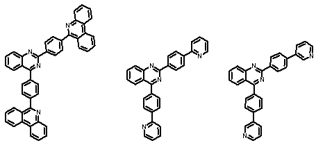 [화학식 A-370] [화학식 A-371] [화학식 A-372][Formula A-370] [Formula A-371] [Formula A-372]
 [화학식 A-373] [화학식 A-374] [화학식 A-375][Formula A-373] [Formula A-374] [Formula A-375]
 [화학식 A-376] [화학식 A-377] [화학식 A-378][Formula A-376] [Formula A-377] [Formula A-378]
 [화학식 A-379] [화학식 A-380] [화학식 A-381][Formula A-379] [Formula A-380] [Formula A-381]
 [화학식 A-382] [화학식 A-383] [화학식 A-384][Formula A-382] [Formula A-383] [Formula A-384]
 [화학식 A-385] [화학식 A-386] [화학식 A-387][Formula A-385] [Formula A-386] [Formula A-387]
 [화학식 A-388] [화학식 A-389] [화학식 A-390][Formula A-388] [Formula A-389] [Formula A-390]
 [화학식 A-391] [화학식 A-392] [화학식 A-393][Formula A-391] [Formula A-392] [Formula A-393]
- 제1항에 있어서,The method of claim 1,상기 유기광전자소자용 화합물은 하기 화학식 B-1 내지 B-30로 표시되는 화합물 중 어느 하나인 것인 유기광전자소자용 화합물.The compound for an organic optoelectronic device is any one of the compounds represented by the formula B-1 to B-30.[화학식 B-1] [화학식 B-2] [화학식 B-3][Formula B-1] [Formula B-2] [Formula B-3]
 [화학식 B-4] [화학식 B-5] [화학식 B-6][Formula B-4] [Formula B-5] [Formula B-6]
 [화학식 B-7] [화학식 B-8] [화학식 B-9][Formula B-7] [Formula B-8] [Formula B-9]
 [화학식 B-10] [화학식 B-11] [화학식 B-12][Formula B-10] [Formula B-11] [Formula B-12]
 [화학식 B-13] [화학식 B-14] [화학식 B-15][Formula B-13] [Formula B-14] [Formula B-15]
 [화학식 B-16] [화학식 B-17] [화학식 B-18][Formula B-16] [Formula B-17] [Formula B-18]
 [화학식 B-19] [화학식 B-20] [화학식 B-21]Formula B-19 Formula B-20 Formula B-21
 [화학식 B-22] [화학식 B-23] [화학식 B-24][Formula B-22] [Formula B-23] [Formula B-24]
 [화학식 B-25] [화학식 B-26] [화학식 B-27][Formula B-25] [Formula B-26] [Formula B-27]
 [화학식 B-28] [화학식 B-29] [화학식 B-30][Formula B-28] [Formula B-29] [Formula B-30]
- 제1항에 있어서,The method of claim 1,상기 유기광전자소자용 화합물은 3중항 여기에너지(T1) 2.0eV 이상인 것인 유기광전자소자용 화합물.The compound for an organic optoelectronic device is a compound for an organic optoelectronic device that is triplet excitation energy (T1) 2.0 eV or more.
- 제1항에 있어서,The method of claim 1,상기 유기광전자소자는, 유기광전소자, 유기발광소자, 유기태양전지, 유기트랜지스터, 유기 감광체 드럼 및 유기메모리소자로 이루어진 군에서 선택되는 것인 유기광전자소자용 화합물.The organic optoelectronic device, an organic optoelectronic device, an organic light emitting device, an organic solar cell, an organic transistor, an organic photoelectric drum, and a compound for an organic optoelectronic device that is selected from the group consisting of an organic memory device.
- 양극, 음극 및 상기 양극과 음극 사이에 개재되는 적어도 한 층 이상의 유기박막층을 포함하는 유기발광소자에 있어서,In an organic light emitting device comprising an anode, a cathode and at least one organic thin film layer interposed between the anode and the cathode,상기 유기박막층 중 적어도 어느 한 층은 상기 제1항에 따른 유기광전자소자용 화합물을 포함하는 것인 유기발광소자.At least one of the organic thin film layer is an organic light emitting device comprising the compound for an organic optoelectronic device according to claim 1.
- 제15항에 있어서,The method of claim 15,상기 유기박막층은 발광층, 정공수송층, 정공주입층, 전자수송층, 전자주입층, 정공차단층 및 이들의 조합으로 이루어진 군에서 선택되는 것인 유기발광소자.The organic thin film layer is selected from the group consisting of a light emitting layer, a hole transport layer, a hole injection layer, an electron transport layer, an electron injection layer, a hole blocking layer and a combination thereof.
- 제16항에 있어서,The method of claim 16,상기 유기광전자소자용 화합물은 전자수송층 또는 전자주입층 내에 포함되는 것인 유기발광소자.The compound for an organic optoelectronic device is an organic light emitting device that is included in the electron transport layer or the electron injection layer.
- 제16항에 있어서,The method of claim 16,상기 유기광전자소자용 화합물은 발광층 내에 포함되는 것인 유기발광소자.The compound for an organic optoelectronic device is included in the light emitting layer.
- 제18항에 있어서,The method of claim 18,상기 유기광전자소자용 화합물은 발광층 내에 인광 또는 형광 호스트 재료로서 사용되는 것인 유기발광소자.The compound for an organic optoelectronic device is used as a phosphorescent or fluorescent host material in the light emitting layer.
- 제15항의 유기발광소자를 포함하는 표시장치.A display device comprising the organic light emitting device of claim 15.
Priority Applications (2)
| Application Number | Priority Date | Filing Date | Title |
|---|---|---|---|
| EP12875420.7A EP2842954B1 (en) | 2012-04-24 | 2012-12-18 | Compound for organic optoelectric device, organic light emitting device containing same, and display device containing said organic light emitting device |
| US14/484,872 US9324948B2 (en) | 2012-04-24 | 2014-09-12 | Compound for organic optoelectronic device, organic light emitting diode including the same and display including the organic light emitting diode |
Applications Claiming Priority (2)
| Application Number | Priority Date | Filing Date | Title |
|---|---|---|---|
| KR1020120042769A KR101531615B1 (en) | 2012-04-24 | 2012-04-24 | Compound for organic optoelectronic device, organic light emitting diode including the same and display including the organic light emitting diode |
| KR10-2012-0042769 | 2012-04-24 |
Related Child Applications (1)
| Application Number | Title | Priority Date | Filing Date |
|---|---|---|---|
| US14/484,872 Continuation-In-Part US9324948B2 (en) | 2012-04-24 | 2014-09-12 | Compound for organic optoelectronic device, organic light emitting diode including the same and display including the organic light emitting diode |
Publications (2)
| Publication Number | Publication Date |
|---|---|
| WO2013162148A1 true WO2013162148A1 (en) | 2013-10-31 |
| WO2013162148A9 WO2013162148A9 (en) | 2014-04-24 |
Family
ID=49483406
Family Applications (1)
| Application Number | Title | Priority Date | Filing Date |
|---|---|---|---|
| PCT/KR2012/011061 WO2013162148A1 (en) | 2012-04-24 | 2012-12-18 | Compound for organic optoelectric device, organic light emitting device containing same, and display device containing said organic light emitting device |
Country Status (4)
| Country | Link |
|---|---|
| US (1) | US9324948B2 (en) |
| EP (1) | EP2842954B1 (en) |
| KR (1) | KR101531615B1 (en) |
| WO (1) | WO2013162148A1 (en) |
Cited By (4)
| Publication number | Priority date | Publication date | Assignee | Title |
|---|---|---|---|---|
| WO2014185592A1 (en) * | 2013-05-13 | 2014-11-20 | 제일모직 주식회사 | Compound for organic optoelectric device, organic light-emitting diode including same, display device including organic light-emitting diode |
| US10797244B2 (en) | 2015-04-28 | 2020-10-06 | Idemitsu Kosan Co., Ltd. | Compound, material for organic electroluminescent element, organic electroluminescent element, and electronic device |
| CN112939890A (en) * | 2021-02-04 | 2021-06-11 | 吉林奥来德光电材料股份有限公司 | Heterocyclic organic photoelectric material, preparation method thereof and organic electroluminescent device |
| CN113195456A (en) * | 2019-05-03 | 2021-07-30 | 株式会社Lg化学 | Heterocyclic compound and organic light emitting device including the same |
Families Citing this family (22)
| Publication number | Priority date | Publication date | Assignee | Title |
|---|---|---|---|---|
| CN104768928B (en) | 2013-03-27 | 2018-06-08 | 出光兴产株式会社 | Condensed fluoranthene compound, material for organic electroluminescent element using same, and organic electroluminescent element and electronic device using same |
| KR102231248B1 (en) * | 2014-04-18 | 2021-03-24 | 덕산네오룩스 주식회사 | Compound for organic electronic element, organic electronic element using the same, and an electronic device thereof |
| KR101897039B1 (en) | 2014-05-22 | 2018-09-10 | 제일모직 주식회사 | Organic compound and composition and organic optoelectric device and display device |
| KR102178087B1 (en) * | 2014-07-03 | 2020-11-12 | 덕산네오룩스 주식회사 | Compound for organic electronic element, organic electronic element using the same, and an electronic device thereof |
| US10403826B2 (en) * | 2015-05-07 | 2019-09-03 | Universal Display Corporation | Organic electroluminescent materials and devices |
| KR101900370B1 (en) * | 2015-05-13 | 2018-09-19 | 삼성에스디아이 주식회사 | Compound for ORGANIC OPTOELECTRIC DEVICE, ORGANIC OPTOELECTRIC DEVICE AND DISPLAY DEVICE |
| WO2016197353A1 (en) * | 2015-06-11 | 2016-12-15 | Dow Global Technologies Llc | Organic electroluminescent compound and organic electroluminescent device comprising the same |
| CN111187225B (en) * | 2015-09-30 | 2021-06-11 | 北京鼎材科技有限公司 | Condensed ring aromatic hydrocarbon derivative with quinoxaline group and application thereof |
| JP6566451B2 (en) * | 2015-12-23 | 2019-08-28 | エルジー・ケム・リミテッド | Compound and organic electronic device containing the same |
| KR20230164202A (en) | 2016-03-15 | 2023-12-01 | 다우 글로벌 테크놀로지스 엘엘씨 | Organic electroluminescent compound and organic electroluminescent device thereof |
| US9985579B2 (en) | 2016-04-12 | 2018-05-29 | Preformed Line Products Co. | Mounting assembly for mounting a solar panel |
| JP6888267B2 (en) * | 2016-10-06 | 2021-06-16 | 三菱ケミカル株式会社 | Iridium complex compounds, compositions containing the compounds, organic electroluminescent devices, display devices and lighting devices. |
| JP7029404B2 (en) * | 2016-10-28 | 2022-03-03 | メルク パテント ゲーエムベーハー | Organic electroluminescence devices and materials for organic electroluminescence |
| CN107383071A (en) * | 2017-07-28 | 2017-11-24 | 长春海谱润斯科技有限公司 | A kind of imidazole derivative and its application |
| CN109293583B (en) * | 2018-10-23 | 2022-03-01 | 西安瑞联新材料股份有限公司 | Quinazoline-containing heterocyclic compound and application thereof in organic photoelectric device |
| CN111747932B (en) * | 2019-03-27 | 2023-09-26 | 北京鼎材科技有限公司 | Compound, application thereof and organic electroluminescent device |
| CN109970716B (en) * | 2019-04-11 | 2020-07-24 | 石家庄诚志永华显示材料有限公司 | Organic compound and application thereof in organic electroluminescent device |
| KR20210086084A (en) * | 2019-12-31 | 2021-07-08 | 엘지디스플레이 주식회사 | Organic compounds and organic light emitting display device having the same |
| CN112420971B (en) * | 2020-11-25 | 2023-04-18 | 合肥福纳科技有限公司 | Method for optimizing light-emitting diode |
| CN115772158A (en) * | 2021-09-06 | 2023-03-10 | 上海和辉光电股份有限公司 | Electron transport material and organic electroluminescent device |
| WO2023099543A1 (en) | 2021-11-30 | 2023-06-08 | Merck Patent Gmbh | Compounds having fluorene structures |
| CN115521253B (en) * | 2022-11-28 | 2023-04-07 | 烟台显华科技集团股份有限公司 | Bibiquinoline derivative compound and application thereof |
Citations (3)
| Publication number | Priority date | Publication date | Assignee | Title |
|---|---|---|---|---|
| WO2004096783A1 (en) * | 2003-04-15 | 2004-11-11 | 3M Innovative Properties Company | Ethynyl containing electron transport agents and their use in organic luminescent devices |
| WO2008066358A1 (en) * | 2006-12-01 | 2008-06-05 | Lg Chem, Ltd. | New compounds and organic light emitting diode using the same |
| WO2011014039A1 (en) * | 2009-07-31 | 2011-02-03 | Rohm And Haas Electronic Materials Korea Ltd. | Novel organic electroluminescent compounds and organic electroluminescent device using the same |
Family Cites Families (12)
| Publication number | Priority date | Publication date | Assignee | Title |
|---|---|---|---|---|
| JP4269382B2 (en) | 1999-01-13 | 2009-05-27 | コニカミノルタホールディングス株式会社 | Organic electroluminescence device |
| US9040170B2 (en) | 2004-09-20 | 2015-05-26 | Global Oled Technology Llc | Electroluminescent device with quinazoline complex emitter |
| JP5266514B2 (en) * | 2005-03-29 | 2013-08-21 | コニカミノルタ株式会社 | Organic electroluminescence device |
| JP4907912B2 (en) | 2005-07-08 | 2012-04-04 | ケミプロ化成株式会社 | Novel 1,3,5-triphenylbenzene derivative and organic electroluminescence device containing the same |
| JP4907192B2 (en) | 2006-02-22 | 2012-03-28 | 東ソー株式会社 | 1,3,5-triazine derivative having pyridyl group, process for producing the same, and organic electroluminescent device comprising the same |
| WO2008015949A1 (en) | 2006-08-04 | 2008-02-07 | Idemitsu Kosan Co., Ltd. | Organic electroluminescence device |
| CN102471679A (en) | 2009-07-10 | 2012-05-23 | 第一毛织株式会社 | Compound for an organic photoelectric element, and an organic photoelectric element comprising the same |
| KR20110013220A (en) | 2009-07-31 | 2011-02-09 | 다우어드밴스드디스플레이머티리얼 유한회사 | Novel organic electroluminescent compounds and organic electroluminescent device using the same |
| KR101387738B1 (en) | 2009-12-29 | 2014-04-22 | 제일모직주식회사 | Compound for organic photoelectric device and organic photoelectric device including the same |
| KR101297158B1 (en) | 2010-02-22 | 2013-08-21 | 제일모직주식회사 | Compound for organic photoelectric device and organic photoelectric device including the same |
| WO2012024132A2 (en) * | 2010-08-16 | 2012-02-23 | University Of Washington Through Its Center For Commercialization | Solution-processable electron-transport materials and related organic optoelectronic devices |
| EP2421064B1 (en) * | 2010-08-18 | 2018-07-04 | Cheil Industries Inc. | Compound for organic optoelectronic device, organic light emmiting diode including the same and display including the light emmiting diode |
-
2012
- 2012-04-24 KR KR1020120042769A patent/KR101531615B1/en active IP Right Grant
- 2012-12-18 WO PCT/KR2012/011061 patent/WO2013162148A1/en active Application Filing
- 2012-12-18 EP EP12875420.7A patent/EP2842954B1/en active Active
-
2014
- 2014-09-12 US US14/484,872 patent/US9324948B2/en active Active
Patent Citations (3)
| Publication number | Priority date | Publication date | Assignee | Title |
|---|---|---|---|---|
| WO2004096783A1 (en) * | 2003-04-15 | 2004-11-11 | 3M Innovative Properties Company | Ethynyl containing electron transport agents and their use in organic luminescent devices |
| WO2008066358A1 (en) * | 2006-12-01 | 2008-06-05 | Lg Chem, Ltd. | New compounds and organic light emitting diode using the same |
| WO2011014039A1 (en) * | 2009-07-31 | 2011-02-03 | Rohm And Haas Electronic Materials Korea Ltd. | Novel organic electroluminescent compounds and organic electroluminescent device using the same |
Non-Patent Citations (2)
| Title |
|---|
| DENG, XIAOHU ET AL.: "Direct, metal-free amination of heterocyclic amides/ureas with NH- heterocycles and N-substituted anilines in POC13", J. ORG. CHEM., vol. 76, 2011, pages 8262 - 8269, XP055159650 * |
| See also references of EP2842954A4 * |
Cited By (5)
| Publication number | Priority date | Publication date | Assignee | Title |
|---|---|---|---|---|
| WO2014185592A1 (en) * | 2013-05-13 | 2014-11-20 | 제일모직 주식회사 | Compound for organic optoelectric device, organic light-emitting diode including same, display device including organic light-emitting diode |
| US9825242B2 (en) | 2013-05-13 | 2017-11-21 | Cheil Industries, Inc. | Compound for organic optoelectric device, organic light-emitting diode including same, display device including organic light-emitting diode |
| US10797244B2 (en) | 2015-04-28 | 2020-10-06 | Idemitsu Kosan Co., Ltd. | Compound, material for organic electroluminescent element, organic electroluminescent element, and electronic device |
| CN113195456A (en) * | 2019-05-03 | 2021-07-30 | 株式会社Lg化学 | Heterocyclic compound and organic light emitting device including the same |
| CN112939890A (en) * | 2021-02-04 | 2021-06-11 | 吉林奥来德光电材料股份有限公司 | Heterocyclic organic photoelectric material, preparation method thereof and organic electroluminescent device |
Also Published As
| Publication number | Publication date |
|---|---|
| EP2842954A4 (en) | 2015-12-16 |
| KR20130119740A (en) | 2013-11-01 |
| KR101531615B1 (en) | 2015-07-02 |
| US20150034938A1 (en) | 2015-02-05 |
| EP2842954B1 (en) | 2020-02-05 |
| WO2013162148A9 (en) | 2014-04-24 |
| EP2842954A1 (en) | 2015-03-04 |
| US9324948B2 (en) | 2016-04-26 |
Similar Documents
| Publication | Publication Date | Title |
|---|---|---|
| WO2013162148A1 (en) | Compound for organic optoelectric device, organic light emitting device containing same, and display device containing said organic light emitting device | |
| WO2011152596A1 (en) | Compound for organic photoelectric device and organic photoelectric device including same | |
| WO2012141393A9 (en) | Compound for organic optoelectronic device, organic light-emitting diode comprising same, and display device comprising the organic light-emitting diode | |
| WO2017074052A1 (en) | Organic light-emitting device | |
| WO2019182360A1 (en) | Compound, organic light-emitting device and display device | |
| WO2020004844A1 (en) | Compound, organic electroluminescent element, and display device | |
| WO2019164327A1 (en) | Organic light-emitting device | |
| WO2011133007A9 (en) | Compound for optoelectronic device, organic light emitting diode including the same and display including the organic light emitting diode | |
| WO2012077902A9 (en) | Compound for an organic optoelectronic device, organic light-emitting diode including the compound, and display device including the organic light-emitting diode | |
| WO2011139055A2 (en) | Compound for organic optoelectronic device, organic light emitting diode including same, and display device including organic light emitting diode | |
| WO2010062065A2 (en) | Novel nitrogen-containing heterocyclic compound and organic electronic device using the same | |
| WO2013094951A1 (en) | Compound for organic optoelectronic device, organic light-emitting diode containing same, and display device comprising organic light-emitting diode | |
| WO2019139419A1 (en) | Organic light-emitting diode | |
| WO2013100540A1 (en) | Compound for organic optoelectronic device, organic light emitting device containing same, and display device containing said organic light emitting device | |
| WO2013100465A1 (en) | Compound for organic optoelectronic element, organic light-emitting element comprising same, and display device comprising the organic light-emitting element | |
| WO2022015084A1 (en) | Organic light-emitting element | |
| WO2012074195A9 (en) | Component for an organic optoelectronic device, organic optoelectronic device including same, and display including the organic optoelectronic device | |
| WO2013022145A1 (en) | Organic optoelectronic device compound and organic light-emitting element including same | |
| WO2013095039A1 (en) | Compound for an organic optoelectronic device, organic light-emitting element comprising same, and display device comprising the organic light-emitting element | |
| WO2018124588A1 (en) | Organic light-emitting device | |
| WO2019135665A1 (en) | Organic light emitting device | |
| WO2011081290A9 (en) | Compound for organic photoelectric device and organic photoelectric device including the compound | |
| WO2020166873A1 (en) | Novel compound and organic light emitting device comprising the same | |
| WO2020022768A1 (en) | Organic light emitting diode | |
| WO2019004787A1 (en) | Organic light emitting element |
Legal Events
| Date | Code | Title | Description |
|---|---|---|---|
| 121 | Ep: the epo has been informed by wipo that ep was designated in this application |
Ref document number: 12875420 Country of ref document: EP Kind code of ref document: A1 |
|
| WWE | Wipo information: entry into national phase |
Ref document number: 2012875420 Country of ref document: EP |
|
| NENP | Non-entry into the national phase |
Ref country code: DE |