WO2013146268A1 - Élément électroluminescent à couche inorganique - Google Patents
Élément électroluminescent à couche inorganique Download PDFInfo
- Publication number
- WO2013146268A1 WO2013146268A1 PCT/JP2013/057007 JP2013057007W WO2013146268A1 WO 2013146268 A1 WO2013146268 A1 WO 2013146268A1 JP 2013057007 W JP2013057007 W JP 2013057007W WO 2013146268 A1 WO2013146268 A1 WO 2013146268A1
- Authority
- WO
- WIPO (PCT)
- Prior art keywords
- metal
- layer
- particles
- range
- light emitting
- Prior art date
Links
- 239000002245 particle Substances 0.000 claims abstract description 653
- 239000002923 metal particle Substances 0.000 claims abstract description 120
- 229910010272 inorganic material Inorganic materials 0.000 claims abstract description 13
- 239000011147 inorganic material Substances 0.000 claims abstract description 13
- 229910052751 metal Inorganic materials 0.000 claims description 453
- 239000002184 metal Substances 0.000 claims description 453
- 238000000862 absorption spectrum Methods 0.000 claims description 60
- 229910052709 silver Inorganic materials 0.000 claims description 52
- 239000004332 silver Substances 0.000 claims description 52
- 239000000463 material Substances 0.000 claims description 43
- 238000002835 absorbance Methods 0.000 claims description 34
- 238000000034 method Methods 0.000 claims description 31
- 230000002708 enhancing effect Effects 0.000 claims description 12
- 238000005424 photoluminescence Methods 0.000 claims description 3
- 238000006862 quantum yield reaction Methods 0.000 claims description 3
- 238000000605 extraction Methods 0.000 abstract description 23
- 230000003321 amplification Effects 0.000 abstract 1
- 238000003199 nucleic acid amplification method Methods 0.000 abstract 1
- 239000010410 layer Substances 0.000 description 456
- 239000000758 substrate Substances 0.000 description 133
- 238000004519 manufacturing process Methods 0.000 description 68
- BQCADISMDOOEFD-UHFFFAOYSA-N Silver Chemical compound [Ag] BQCADISMDOOEFD-UHFFFAOYSA-N 0.000 description 51
- 230000000694 effects Effects 0.000 description 40
- 230000000052 comparative effect Effects 0.000 description 35
- 239000010408 film Substances 0.000 description 25
- 239000011521 glass Substances 0.000 description 22
- 239000002105 nanoparticle Substances 0.000 description 21
- 238000001878 scanning electron micrograph Methods 0.000 description 16
- 230000003993 interaction Effects 0.000 description 15
- 238000000089 atomic force micrograph Methods 0.000 description 11
- 230000005284 excitation Effects 0.000 description 11
- 239000000243 solution Substances 0.000 description 11
- CDBYLPFSWZWCQE-UHFFFAOYSA-L Sodium Carbonate Chemical compound [Na+].[Na+].[O-]C([O-])=O CDBYLPFSWZWCQE-UHFFFAOYSA-L 0.000 description 10
- 230000009471 action Effects 0.000 description 10
- 238000005253 cladding Methods 0.000 description 10
- 238000005259 measurement Methods 0.000 description 10
- 239000002082 metal nanoparticle Substances 0.000 description 10
- 238000004544 sputter deposition Methods 0.000 description 10
- CSCPPACGZOOCGX-UHFFFAOYSA-N Acetone Chemical compound CC(C)=O CSCPPACGZOOCGX-UHFFFAOYSA-N 0.000 description 8
- 239000006185 dispersion Substances 0.000 description 8
- 239000007769 metal material Substances 0.000 description 8
- 238000005401 electroluminescence Methods 0.000 description 7
- 230000006870 function Effects 0.000 description 6
- 239000011248 coating agent Substances 0.000 description 5
- 238000000576 coating method Methods 0.000 description 5
- 238000000295 emission spectrum Methods 0.000 description 5
- 239000003574 free electron Substances 0.000 description 5
- 239000000126 substance Substances 0.000 description 5
- 239000010409 thin film Substances 0.000 description 5
- KDLHZDBZIXYQEI-UHFFFAOYSA-N Palladium Chemical compound [Pd] KDLHZDBZIXYQEI-UHFFFAOYSA-N 0.000 description 4
- OAICVXFJPJFONN-UHFFFAOYSA-N Phosphorus Chemical compound [P] OAICVXFJPJFONN-UHFFFAOYSA-N 0.000 description 4
- XKRFYHLGVUSROY-UHFFFAOYSA-N argon Substances [Ar] XKRFYHLGVUSROY-UHFFFAOYSA-N 0.000 description 4
- 238000010586 diagram Methods 0.000 description 4
- 230000001678 irradiating effect Effects 0.000 description 4
- 229910000510 noble metal Inorganic materials 0.000 description 4
- BASFCYQUMIYNBI-UHFFFAOYSA-N platinum Chemical compound [Pt] BASFCYQUMIYNBI-UHFFFAOYSA-N 0.000 description 4
- 230000008569 process Effects 0.000 description 4
- KFZMGEQAYNKOFK-UHFFFAOYSA-N Isopropanol Chemical compound CC(C)O KFZMGEQAYNKOFK-UHFFFAOYSA-N 0.000 description 3
- SECXISVLQFMRJM-UHFFFAOYSA-N N-Methylpyrrolidone Chemical compound CN1CCCC1=O SECXISVLQFMRJM-UHFFFAOYSA-N 0.000 description 3
- 229910052786 argon Inorganic materials 0.000 description 3
- 230000009849 deactivation Effects 0.000 description 3
- 238000000151 deposition Methods 0.000 description 3
- 230000008021 deposition Effects 0.000 description 3
- 238000011049 filling Methods 0.000 description 3
- 239000010419 fine particle Substances 0.000 description 3
- 238000000691 measurement method Methods 0.000 description 3
- 230000007246 mechanism Effects 0.000 description 3
- 150000002739 metals Chemical class 0.000 description 3
- 230000027756 respiratory electron transport chain Effects 0.000 description 3
- XLYOFNOQVPJJNP-UHFFFAOYSA-N water Substances O XLYOFNOQVPJJNP-UHFFFAOYSA-N 0.000 description 3
- RYGMFSIKBFXOCR-UHFFFAOYSA-N Copper Chemical compound [Cu] RYGMFSIKBFXOCR-UHFFFAOYSA-N 0.000 description 2
- LFQSCWFLJHTTHZ-UHFFFAOYSA-N Ethanol Chemical compound CCO LFQSCWFLJHTTHZ-UHFFFAOYSA-N 0.000 description 2
- 229910004298 SiO 2 Inorganic materials 0.000 description 2
- -1 argon ion Chemical class 0.000 description 2
- 230000008901 benefit Effects 0.000 description 2
- 239000000470 constituent Substances 0.000 description 2
- 229910052802 copper Inorganic materials 0.000 description 2
- 239000010949 copper Substances 0.000 description 2
- 230000005684 electric field Effects 0.000 description 2
- 238000005530 etching Methods 0.000 description 2
- 238000002474 experimental method Methods 0.000 description 2
- 239000007789 gas Substances 0.000 description 2
- PCHJSUWPFVWCPO-UHFFFAOYSA-N gold Chemical compound [Au] PCHJSUWPFVWCPO-UHFFFAOYSA-N 0.000 description 2
- 229910052737 gold Inorganic materials 0.000 description 2
- 239000010931 gold Substances 0.000 description 2
- 230000006872 improvement Effects 0.000 description 2
- 238000002347 injection Methods 0.000 description 2
- 239000007924 injection Substances 0.000 description 2
- 230000031700 light absorption Effects 0.000 description 2
- 238000004020 luminiscence type Methods 0.000 description 2
- 238000001755 magnetron sputter deposition Methods 0.000 description 2
- 239000012528 membrane Substances 0.000 description 2
- 230000003287 optical effect Effects 0.000 description 2
- 229910052763 palladium Inorganic materials 0.000 description 2
- 229910052697 platinum Inorganic materials 0.000 description 2
- 238000002360 preparation method Methods 0.000 description 2
- 238000011160 research Methods 0.000 description 2
- 239000004094 surface-active agent Substances 0.000 description 2
- 238000007740 vapor deposition Methods 0.000 description 2
- 238000012935 Averaging Methods 0.000 description 1
- 241000338702 Cupido minimus Species 0.000 description 1
- 238000010521 absorption reaction Methods 0.000 description 1
- 229910045601 alloy Inorganic materials 0.000 description 1
- 239000000956 alloy Substances 0.000 description 1
- 229910052782 aluminium Inorganic materials 0.000 description 1
- XAGFODPZIPBFFR-UHFFFAOYSA-N aluminium Chemical compound [Al] XAGFODPZIPBFFR-UHFFFAOYSA-N 0.000 description 1
- 238000013459 approach Methods 0.000 description 1
- 238000000429 assembly Methods 0.000 description 1
- 230000000712 assembly Effects 0.000 description 1
- 230000004888 barrier function Effects 0.000 description 1
- 238000005266 casting Methods 0.000 description 1
- 238000005229 chemical vapour deposition Methods 0.000 description 1
- 239000011258 core-shell material Substances 0.000 description 1
- 230000003247 decreasing effect Effects 0.000 description 1
- 230000006866 deterioration Effects 0.000 description 1
- 238000009792 diffusion process Methods 0.000 description 1
- KPUWHANPEXNPJT-UHFFFAOYSA-N disiloxane Chemical class [SiH3]O[SiH3] KPUWHANPEXNPJT-UHFFFAOYSA-N 0.000 description 1
- 238000010292 electrical insulation Methods 0.000 description 1
- 238000000609 electron-beam lithography Methods 0.000 description 1
- 238000005516 engineering process Methods 0.000 description 1
- 238000011156 evaluation Methods 0.000 description 1
- 230000005281 excited state Effects 0.000 description 1
- 230000001747 exhibiting effect Effects 0.000 description 1
- 230000005283 ground state Effects 0.000 description 1
- 230000001939 inductive effect Effects 0.000 description 1
- 239000011810 insulating material Substances 0.000 description 1
- 150000002500 ions Chemical class 0.000 description 1
- 238000010030 laminating Methods 0.000 description 1
- 239000002346 layers by function Substances 0.000 description 1
- 239000007788 liquid Substances 0.000 description 1
- 150000002736 metal compounds Chemical class 0.000 description 1
- 229910044991 metal oxide Inorganic materials 0.000 description 1
- 150000004706 metal oxides Chemical class 0.000 description 1
- 238000002488 metal-organic chemical vapour deposition Methods 0.000 description 1
- 239000010445 mica Substances 0.000 description 1
- 229910052618 mica group Inorganic materials 0.000 description 1
- 239000002086 nanomaterial Substances 0.000 description 1
- 230000010355 oscillation Effects 0.000 description 1
- 239000003973 paint Substances 0.000 description 1
- 238000012805 post-processing Methods 0.000 description 1
- 239000011241 protective layer Substances 0.000 description 1
- 230000009467 reduction Effects 0.000 description 1
- 150000003839 salts Chemical class 0.000 description 1
- 229910052594 sapphire Inorganic materials 0.000 description 1
- 239000010980 sapphire Substances 0.000 description 1
- 239000004065 semiconductor Substances 0.000 description 1
- 239000002356 single layer Substances 0.000 description 1
- 229910052715 tantalum Inorganic materials 0.000 description 1
- GUVRBAGPIYLISA-UHFFFAOYSA-N tantalum atom Chemical compound [Ta] GUVRBAGPIYLISA-UHFFFAOYSA-N 0.000 description 1
- 238000000870 ultraviolet spectroscopy Methods 0.000 description 1
- 238000001771 vacuum deposition Methods 0.000 description 1
Images


Classifications
-
- H—ELECTRICITY
- H01—ELECTRIC ELEMENTS
- H01L—SEMICONDUCTOR DEVICES NOT COVERED BY CLASS H10
- H01L33/00—Semiconductor devices having potential barriers specially adapted for light emission; Processes or apparatus specially adapted for the manufacture or treatment thereof or of parts thereof; Details thereof
- H01L33/02—Semiconductor devices having potential barriers specially adapted for light emission; Processes or apparatus specially adapted for the manufacture or treatment thereof or of parts thereof; Details thereof characterised by the semiconductor bodies
- H01L33/04—Semiconductor devices having potential barriers specially adapted for light emission; Processes or apparatus specially adapted for the manufacture or treatment thereof or of parts thereof; Details thereof characterised by the semiconductor bodies with a quantum effect structure or superlattice, e.g. tunnel junction
- H01L33/06—Semiconductor devices having potential barriers specially adapted for light emission; Processes or apparatus specially adapted for the manufacture or treatment thereof or of parts thereof; Details thereof characterised by the semiconductor bodies with a quantum effect structure or superlattice, e.g. tunnel junction within the light emitting region, e.g. quantum confinement structure or tunnel barrier
-
- H—ELECTRICITY
- H01—ELECTRIC ELEMENTS
- H01L—SEMICONDUCTOR DEVICES NOT COVERED BY CLASS H10
- H01L33/00—Semiconductor devices having potential barriers specially adapted for light emission; Processes or apparatus specially adapted for the manufacture or treatment thereof or of parts thereof; Details thereof
- H01L33/02—Semiconductor devices having potential barriers specially adapted for light emission; Processes or apparatus specially adapted for the manufacture or treatment thereof or of parts thereof; Details thereof characterised by the semiconductor bodies
- H01L33/04—Semiconductor devices having potential barriers specially adapted for light emission; Processes or apparatus specially adapted for the manufacture or treatment thereof or of parts thereof; Details thereof characterised by the semiconductor bodies with a quantum effect structure or superlattice, e.g. tunnel junction
-
- H—ELECTRICITY
- H01—ELECTRIC ELEMENTS
- H01L—SEMICONDUCTOR DEVICES NOT COVERED BY CLASS H10
- H01L33/00—Semiconductor devices having potential barriers specially adapted for light emission; Processes or apparatus specially adapted for the manufacture or treatment thereof or of parts thereof; Details thereof
- H01L33/48—Semiconductor devices having potential barriers specially adapted for light emission; Processes or apparatus specially adapted for the manufacture or treatment thereof or of parts thereof; Details thereof characterised by the semiconductor body packages
- H01L33/50—Wavelength conversion elements
- H01L33/501—Wavelength conversion elements characterised by the materials, e.g. binder
- H01L33/502—Wavelength conversion materials
-
- H—ELECTRICITY
- H05—ELECTRIC TECHNIQUES NOT OTHERWISE PROVIDED FOR
- H05B—ELECTRIC HEATING; ELECTRIC LIGHT SOURCES NOT OTHERWISE PROVIDED FOR; CIRCUIT ARRANGEMENTS FOR ELECTRIC LIGHT SOURCES, IN GENERAL
- H05B33/00—Electroluminescent light sources
- H05B33/12—Light sources with substantially two-dimensional radiating surfaces
- H05B33/14—Light sources with substantially two-dimensional radiating surfaces characterised by the chemical or physical composition or the arrangement of the electroluminescent material, or by the simultaneous addition of the electroluminescent material in or onto the light source
-
- H—ELECTRICITY
- H01—ELECTRIC ELEMENTS
- H01L—SEMICONDUCTOR DEVICES NOT COVERED BY CLASS H10
- H01L33/00—Semiconductor devices having potential barriers specially adapted for light emission; Processes or apparatus specially adapted for the manufacture or treatment thereof or of parts thereof; Details thereof
- H01L33/02—Semiconductor devices having potential barriers specially adapted for light emission; Processes or apparatus specially adapted for the manufacture or treatment thereof or of parts thereof; Details thereof characterised by the semiconductor bodies
- H01L33/20—Semiconductor devices having potential barriers specially adapted for light emission; Processes or apparatus specially adapted for the manufacture or treatment thereof or of parts thereof; Details thereof characterised by the semiconductor bodies with a particular shape, e.g. curved or truncated substrate
- H01L33/22—Roughened surfaces, e.g. at the interface between epitaxial layers
-
- H—ELECTRICITY
- H01—ELECTRIC ELEMENTS
- H01L—SEMICONDUCTOR DEVICES NOT COVERED BY CLASS H10
- H01L33/00—Semiconductor devices having potential barriers specially adapted for light emission; Processes or apparatus specially adapted for the manufacture or treatment thereof or of parts thereof; Details thereof
- H01L33/44—Semiconductor devices having potential barriers specially adapted for light emission; Processes or apparatus specially adapted for the manufacture or treatment thereof or of parts thereof; Details thereof characterised by the coatings, e.g. passivation layer or anti-reflective coating
- H01L33/46—Reflective coating, e.g. dielectric Bragg reflector
Definitions
- the present invention relates to an inorganic layer light emitting device such as an inorganic LED device (inorganic light emitting diode device) or an inorganic EL device (inorganic electroluminescent device) whose light emission is enhanced by utilizing plasmon resonance of a metal-based particle aggregate.
- an inorganic layer light emitting device such as an inorganic LED device (inorganic light emitting diode device) or an inorganic EL device (inorganic electroluminescent device) whose light emission is enhanced by utilizing plasmon resonance of a metal-based particle aggregate.
- Plasmon is a free-electron rough wave generated by collective oscillation of free electrons in a metal nanostructure.
- Patent Document 1 discloses a technique for enhancing the fluorescence of a fluorescent substance using a localized plasmon resonance phenomenon.
- Patent Document 2 discloses a technique for enhancing the fluorescence of a fluorescent substance using a localized plasmon resonance phenomenon.
- Patent Document 3 discloses a technique for enhancing the fluorescence of a fluorescent substance using a localized plasmon resonance phenomenon.
- Patent Document 2 discloses an electroluminescence (EL) device in which core-shell type fine particles capable of inducing localized plasmons comprising a metal fine particle core and an insulating shell covering the metal fine particle core are arranged in the vicinity of or inside the light emitting region.
- EL electroluminescence
- Non-Patent Document 1 Studies on localized plasmon resonance by nanoparticles are shown.
- the luminous efficiency of inorganic LED elements and inorganic EL elements to which metal nanoparticles are applied as a plasmon material remains at a relatively low value for the following reasons, and there is a strong demand for improvement.
- the emission enhancement effect by plasmon resonance itself is not relatively strong, and the range of the emission enhancement effect (the action of localized plasmon resonance). The range) is extremely narrow, and the light emission enhancement effect can be obtained only in a very small part of the light emitting layer, so that there is a problem that a sufficient light emission enhancement effect cannot be obtained.
- metal nanoparticles in the vicinity of or inside the light emitting layer as described in Patent Document 2, but in this case, the metal nanoparticles and the light extraction surface At the interface between the layers interposed therebetween, at least a part of the emitted light is reflected in a direction different from the light extraction surface, causing a problem that the light extraction efficiency is lowered.
- the metal nanoparticles are arranged in the vicinity of the light extraction surface, and in order to reduce the distance between the light emitting layer and the metal nanoparticles, a layer (for example, a cladding layer) interposed between the metal nanoparticles and the light extraction surface is used.
- a layer for example, a cladding layer
- an object of the present invention is to provide an inorganic layer light emitting device exhibiting high light emission efficiency by enhancing light emission and improving light extraction efficiency by a novel plasmon material.
- Patent Document 1 paragraphs 0010 to 0011
- the particle size is about 500 nm.
- the luminous efficiency ⁇ is theoretically about 1
- such a silver particle does not exhibit a light emission enhancing action in practice.
- the reason why such large silver particles show almost no light emission enhancement is because the surface free electrons in the silver particles are so large that the bipolars seen in general nanoparticles (relatively small nanoparticles) This is presumably because child-type localized plasmons hardly occur.
- the enhancement effect by plasmons can be dramatically improved.
- the present inventor made large metal particles, which are generally considered to have a reduced light emission enhancement effect as described above, to have a specific shape, and arranged more than a specific number thereof in two dimensions.
- the metal-based particle aggregate not only exhibits extremely strong plasmon resonance, but can significantly extend the range of action of plasmon resonance (the range in which the plasmon enhances), and such metal-based particle aggregates. It has been found that the luminous efficiency can be remarkably improved by disposing a layer (film) made of the above in an inorganic layer light emitting element.
- a light emitting layer including a light emitter made of an inorganic material;
- a metal-based particle assembly layer having an aspect ratio defined by a ratio of the average particle diameter to the average height in a range of 1 to 8 in a range of 55 to 500 nm;
- the inorganic layer light-emitting element in which the metal particles constituting the metal particle aggregate layer are arranged so that the average distance between the metal particles is 1 to 150 nm.
- a light emitting layer including a light emitter made of an inorganic material;
- a metal-based particle assembly layer having an aspect ratio defined by a ratio of the average particle diameter to the average height in a range of 1 to 8 in a range of 55 to 500 nm; With In the absorption spectrum in the visible light region, the metal-based particle assembly layer has the same particle diameter as the average particle diameter, the same height as the average height and the same material, and the distance between the metal particles is the same.
- the peak maximum wavelength on the longest wavelength side is shifted to the short wavelength side in the range of 30 to 500 nm.
- Inorganic layer light emitting device Compared to the reference metal-based particle aggregate (X) arranged so as to be all in the range of 1 to 2 ⁇ m, the peak maximum wavelength on the longest wavelength side is shifted to the short wavelength side in the range of 30 to 500 nm. Inorganic layer light emitting device.
- a light emitting layer including a light emitter made of an inorganic material;
- a metal-based particle assembly layer having an aspect ratio defined by a ratio of the average particle diameter to the average height in a range of 1 to 8 in a range of 55 to 500 nm; With In the absorption spectrum in the visible light region, the metal-based particle assembly layer has the same particle diameter as the average particle diameter, the same height as the average height and the same material, and the distance between the metal particles is the same.
- the inorganic material Compared to the reference metal particle aggregate (Y) arranged so as to be in the range of 1 to 2 ⁇ m, the inorganic material has higher absorbance at the maximum wavelength of the peak on the longest wavelength side in comparison with the same number of metal particles. Layer light emitting device.
- the metal-based particle assembly layer has any one of [1] to [6], wherein a peak on the longest wavelength side has a maximum wavelength in a range of 350 to 550 nm in an absorption spectrum in a visible light region.
- the distance from the light emitting layer side surface of the metal-based particle assembly layer to the light-emitting layer is 20 nm or more, and the photoluminescence quantum yield of the light-emitting material contained in the light-emitting layer is the metal-based particle.
- the inorganic layer light emitting device according to any one of [1] to [12], which is 1.5 times or more as compared with a reference inorganic layer light emitting device having no aggregate layer.
- the average height is in the range of 55 to 500 nm, the aspect ratio defined by the ratio of the average particle diameter to the average height is in the range of 1 to 8, and the metal-based particles are the adjacent metal-based particles.
- a method for enhancing light emission of an inorganic layer light emitting device comprising disposing a metal-based particle assembly layer disposed so that an average distance from the particles is within a range of 1 to 150 nm in the inorganic layer light emitting device.
- the average height is in the range of 55 to 500 nm
- the aspect ratio defined by the ratio of the average particle diameter to the average height is in the range of 1 to 8
- the average in the absorption spectrum in the visible light region Reference metal particle aggregate in which metal particles made of the same particle size, the same height as the average height, and the same material are arranged so that the distance between the metal particles is all within the range of 1 to 2 ⁇ m.
- a metal-based particle assembly layer in which the peak maximum wavelength on the longest wavelength side is shifted to the short wavelength side in the range of 30 to 500 nm is disposed in the inorganic layer light emitting device.
- Inorganic features Emission enhancement method of the light-emitting element.
- the average height is in the range of 55 to 500 nm
- the aspect ratio defined by the ratio of the average particle diameter to the average height is in the range of 1 to 8
- the average in the absorption spectrum in the visible light region Reference metal particle aggregate in which metal particles made of the same particle size, the same height as the average height, and the same material are arranged so that the distance between the metal particles is all within the range of 1 to 2 ⁇ m.
- the metal particle assembly layer having a higher absorbance at the maximum wavelength of the peak on the longest wavelength side is disposed in the inorganic layer light emitting device. None to do Emission enhancement method of the layer emitting element.
- the “inorganic layer light emitting device” means a light emitting device having a light emitting layer made of an inorganic material, and includes “inorganic LED device (inorganic light emitting diode device)” and “inorganic EL device (inorganic electroluminescent device). Luminescence element) ".
- “Inorganic LED element” means an inorganic semiconductor light-emitting element that generates excitons by injecting electrons and holes into the light-emitting layer and emits them. The light-emitting layer is excited by electrons accelerated by an external electric field. It is distinguished from an “inorganic EL element” that emits light when the state returns to the ground state.
- the light emitting layer may have a single layer structure or a multilayer structure in which, for example, quantum well layers and barrier layers are alternately stacked. In the latter case, the thickness of the light emitting layer refers to the total thickness of the multilayer structure.
- inorganic layer light emission with high light emission efficiency is achieved by providing a metal-based particle assembly layer having plasmon characteristics not found in conventional plasmon materials, thereby improving light emission and improving light extraction efficiency.
- An element can be provided.
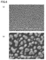
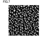
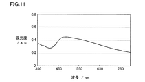
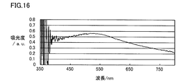
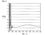
- 6 is an AFM image of a metal-based particle assembly layer in a metal-based particle assembly layer laminated substrate obtained in Production Example 2. It is a SEM image (10000 time scale) when the metal type particle assembly layer in the metal type particle assembly layer laminated substrate obtained in Comparative Production Example 3 is viewed from directly above. 6 is an AFM image of a metal-based particle assembly layer in a metal-based particle assembly layer laminated substrate obtained in Comparative Production Example 3. 4 is an absorption spectrum of the metal-based particle assembly layer laminated substrate obtained in Production Example 1 and Comparative Production Examples 1-2.
- FIG. 4 is an absorption spectrum of a metal-based particle assembly layer laminated substrate obtained in Production Example 2. It is a schematic flowchart which shows the manufacturing method of a reference metal type particle aggregate. It is a SEM image (20000 times and 50000 times scale) when the reference metal type particle assembly layer in a reference metal type particle assembly layer laminated substrate is seen from right above. It is a figure explaining the absorption-spectrum measuring method using the objective lens (100 times) of a microscope. It is the light absorption spectrum of the metal type particle assembly layer laminated substrate obtained by the manufacture example 1 measured by the method using the objective lens (100 times) of a microscope.
- the inorganic layer light emitting device of the present invention is disposed in an inorganic layer light emitting device in which a light emitting layer including a phosphor made of an inorganic material and 30 or more metal-based particles are two-dimensionally arranged apart from each other. And at least a metal-based particle assembly layer that is a layer (film) made of a particle assembly.
- the metal-based particles constituting the metal-based particle assembly layer have an average particle diameter in the range of 200 to 1600 nm, an average height in the range of 55 to 500 nm, and the ratio of the average particle diameter to the average height.
- the aspect ratio defined by 1 is in the range of 1-8.
- the metal-based particle assembly layer has any of the following characteristics.
- the metal-based particles constituting the metal-based particle assembly layer are arranged so that the average distance from the adjacent metal-based particles is within a range of 1 to 150 nm (first embodiment).
- the metal-based particle assembly layer has a same particle diameter, the same height as the average height, and the same material in the absorption spectrum in the visible light region. Compared to the reference metal particle aggregate (X) arranged so that the distances are all in the range of 1 to 2 ⁇ m, the maximum wavelength of the peak on the longest wavelength side is shifted to the short wavelength side in the range of 30 to 500 nm.
- the metal-based particle assembly layer has a same particle diameter as the average particle diameter, the same height as the average height, and the same material in the absorption spectrum in the visible light region. Compared with the same number of metal particles compared to the reference metal particle aggregate (Y) arranged so that the distances are all within the range of 1 to 2 ⁇ m, the absorbance at the maximum wavelength of the peak on the longest wavelength side is larger. High (third embodiment).
- the average particle diameter and average height of the metal-based particle aggregate are “same” as that of the reference metal-based particle aggregate (X) or (Y).
- the difference in average particle diameter is ⁇ 5 nm. It means that the difference in average height is within a range of ⁇ 10 nm.
- the intensity of plasmon resonance exhibited by the metal-based particle assembly layer according to the present embodiment is not a mere summation of localized plasmon resonance exhibited by individual metal-based particles at a specific wavelength, but is higher than that. That is, when 30 or more metal particles having a predetermined shape are densely arranged at the predetermined interval, individual metal particles interact with each other, and extremely strong plasmon resonance is expressed. This is considered to be expressed by the interaction between the localized plasmons of the metal-based particles.
- a plasmon resonance peak (hereinafter also referred to as a plasmon peak) is observed as a peak in the ultraviolet to visible region.
- the strength of the plasmon resonance of the plasmon material can be roughly evaluated, but the metal-based particle assembly layer according to the present embodiment is measured when the absorption spectrum is measured in a state of being laminated on a glass substrate.
- the absorbance at the maximum wavelength of the plasmon peak on the longest wavelength side in the visible light region can be 1 or more, further 1.5 or more, and even about 2.
- the absorption spectrum of the metal-based particle assembly layer is measured in a state of being laminated on a glass substrate by absorptiometry. Specifically, the absorption spectrum is from the back side of the glass substrate on which the metal-based particle assembly layer is laminated (the side opposite to the metal-based particle assembly layer), and is ultraviolet to visible from the direction perpendicular to the substrate surface.
- a substrate having the same thickness and material as the substrate of the metal particle assembly film laminated substrate, and the intensity I of transmitted light in all directions irradiated with incident light in the light region and transmitted to the metal particle assembly layer side; Irradiating the same incident light from the direction perpendicular to the surface of the substrate on which the metal-based particle assembly film is not laminated, and integrating the transmitted light intensity I 0 in all directions transmitted from the opposite side of the incident surface. It is obtained by measuring using a sphere spectrophotometer. At this time, the absorbance, which is the vertical axis of the absorption spectrum, has the following formula: Absorbance ⁇ log 10 (I / I 0 ) It is represented by
- the action range of plasmon resonance by the metal-based particle assembly layer (the range where the enhancement effect by plasmon is extended) is remarkably extended. Therefore, a stronger emission enhancement effect is obtained compared to the case of using a conventional plasmon material. As described above, this contributes to a dramatic improvement in luminous efficiency. In other words, the substantial extension of the working range makes it possible to simultaneously enhance the entire light emitting layer even when the thickness of the light emitting layer is large, thereby significantly improving the light emission efficiency of the inorganic layer light emitting element. it can.
- Such an elongation action is also considered to be manifested by the interaction between localized plasmons of metal-based particles produced by densely arranging 30 or more predetermined-shaped metal particles at a predetermined interval.
- the plasmon resonance operating range can be extended to, for example, about several hundred nm.
- the metal-based particle aggregate is located at a position separated from the light emitting layer by, for example, 10 nm, further several tens of nm (for example, more than 20 nm, 30 nm, or 40 nm), and even several hundred nm. Even if the layers are arranged, the enhancement effect by plasmon resonance can be obtained.
- the metal-based particle assembly layer which is a plasmon material, can be placed closer to the light extraction surface than the light-emitting layer, and further, the metal-based particle assembly layer can be disposed in the vicinity of the light extraction surface that is considerably away from the light-emitting layer.
- the light extraction efficiency can be greatly improved.
- the plasmon material is disposed very close to or inside the light emitting layer, at least a part of the emitted light is extracted at the interface of each layer interposed between the plasmon material and the light extraction surface.
- the light extraction efficiency was reduced due to reflection in a direction different from the surface.
- the metal-based particle assembly layer according to the present embodiment does not use dipole-type localized plasmons alone, although relatively large metal-based particles are used in the visible light region.
- a large number of large metal-based particles (although it is necessary to have a predetermined shape) are densely arranged at specific intervals so that the large-sized metal particles are included.
- An extremely large number of surface free electrons can be excited as plasmons, and it is possible to realize extremely strong plasmon resonance in the inorganic layer light emitting device and a significant extension of the plasmon resonance operating range.
- a specific number or more of relatively large metal particles in which the metal particle aggregate layer has a specific shape is two-dimensionally spaced at a specific interval. Due to the structure, the following advantageous effects can be obtained.
- the maximal wavelength of the plasmon peak is a specific shift depending on the average particle diameter and the average interparticle distance of the metal-based particles. Therefore, it is possible to particularly enhance the light emission in a specific (desired) wavelength region. Specifically, the maximum wavelength of the plasmon peak on the longest wavelength side in the visible light region shifts to the short wavelength side (blue shift) as the average particle size of the metal-based particles increases with a constant average interparticle distance. To do.
- the maximum of the plasmon peak on the longest wavelength side in the visible light region The wavelength shifts to the short wavelength side.
- This unique phenomenon is due to the Mie scattering theory generally accepted for plasmon materials (according to this theory, the maximum wavelength of the plasmon peak shifts to the longer wavelength side (red shift) as the particle size increases). It is contrary.
- the peculiar blue shift as described above also has a structure in which the metal-based particle aggregate layer has large metal particles densely arranged at specific intervals. This is thought to be due to the interaction between plasmons.
- the metal-based particle assembly layer (in a state of being laminated on a glass substrate) according to the present embodiment is an absorption spectrum in the visible light region measured by an absorptiometry according to the shape of the metal-based particles and the average interparticle distance.
- the plasmon peak on the longest wavelength side can exhibit a maximum wavelength in a wavelength region of 350 to 550 nm, for example.
- the metal-based particle assembly layer according to the present embodiment typically has a thickness of about 30 to 500 nm as compared with the case where the metal-based particles are arranged with a sufficiently long inter-particle distance (for example, 1 ⁇ m) ( For example, a blue shift of 30 to 250 nm may occur.
- Such metal-based particle assembly layers in which the maximum wavelength of the plasmon peak is blue-shifted are particularly strongly required to improve luminous efficiency. It is useful as an enhancement element for an inorganic layer light emitting device that emits light in the blue or near wavelength region.
- the metal-based particles constituting the metal-based particle assembly layer are not particularly limited as long as they are made of a material having a plasmon peak in the ultraviolet to visible region in the absorption spectrum measurement by absorptiometry when it is a nanoparticle or an aggregate thereof.
- noble metals such as gold, silver, copper, platinum and palladium, metals such as aluminum and tantalum; the noble metals or alloys containing metals; metal compounds including the noble metals or metals (metal oxides, metal salts, etc. ).
- noble metals such as gold, silver, copper, platinum, and palladium are preferable, and silver is more preferable because it is inexpensive and has low absorption (small imaginary part of dielectric function at visible light wavelength).
- the average particle diameter of the metal-based particles is in the range of 200 to 1600 nm.
- the metal-based particle assembly layer according to the present embodiment has a remarkably strong plasmon resonance and plasmon resonance by arranging a predetermined number (30) or more of such large metal-based particles densely at a predetermined interval. The remarkable extension of the action range of resonance and the effect (3) are realized.
- the average particle diameter of the metal-based particles refers to 10 particles randomly selected from the SEM observation image directly above the metal-based particle assembly layer in which the metal-based particles are two-dimensionally arranged. Randomly draw 5 tangential diameters in the particle image (however, any straight line with a tangential diameter can only pass through the interior of the particle image, one of which is only the interior of the particle and can be drawn the longest) The average value of the 10 selected particle sizes when the average value is the particle size of each particle.
- the tangent diameter is defined as a perpendicular line connecting the interval (projection image) of a particle between two parallel lines in contact with it (Nikkan Kogyo Shimbun, “Particle Measurement Technology”, 1994, page 5). .
- the average height of the metal-based particles is in the range of 55 to 500 nm, and in order to effectively obtain the effects (1) to (3), preferably in the range of 55 to 300 nm, more preferably 70 to 150 nm. It is.
- the average height of the metal-based particles is 10 particles when 10 particles are selected at random in the AFM observation image of the metal-based particle assembly layer (film) and the heights of these 10 particles are measured. Is the average value of the measured values.
- the aspect ratio of the metal-based particles is in the range of 1 to 8, and preferably 2 to 8, more preferably 2.5 to 8 in order to effectively obtain the effects (1) to (3). Is within.
- the aspect ratio of the metal-based particles is defined by the ratio of the average particle diameter to the average height (average particle diameter / average height).
- the metal-based particles may be spherical, but for the above reasons, the metal particles preferably have a flat shape with an aspect ratio exceeding 1.
- the metal particles preferably have a smooth curved surface, and more preferably have a flat shape with a smooth curved surface. Some minute irregularities (roughness) may be included, and in this sense, the metal-based particles may be indefinite.
- the size variation between the metal-based particles is as small as possible.
- the distance between the large particles is increased, and it is preferable that the interaction between the large particles is facilitated by filling the space between the small particles.
- the metal-based particles are arranged so that the average distance between the adjacent metal-based particles (average interparticle distance) is in the range of 1 to 150 nm.
- the average interparticle distance is preferably in the range of 1 to 100 nm, more preferably 1 to 50 nm, and even more preferably 1 to 20 nm in order to effectively obtain the effects (1) to (3).
- the average interparticle distance is less than 1 nm, electron transfer based on the Dexter mechanism occurs between particles, which is disadvantageous in terms of deactivation of localized plasmons.
- the average inter-particle distance here refers to 30 randomly selected particles in the SEM observation image from directly above the metal-based particle assembly layer in which the metal-based particles are two-dimensionally arranged, It is an average value of the interparticle distances of these 30 particles when the interparticle distance between adjacent particles is determined.
- the inter-particle distance between adjacent particles is a value obtained by measuring the distances between all adjacent particles (the distance between the surfaces) and averaging them.
- the number of metal particles contained in the metal particle aggregate layer is 30 or more, preferably 50 or more.
- the number of metal-based particles contained in the metal-based particle aggregate can be, for example, 300 or more, and further 17500 or more.
- the number density of the metal particles in the metal particle assembly layer is preferably 7 particles / ⁇ m 2 or more, and more preferably 15 particles / ⁇ m 2 or more.
- the metal-based particles are insulated from each other, in other words, non-conductive (non-conductive as a metal-based particle assembly layer) between adjacent metal-based particles. Is preferred. When electrons can be exchanged between some or all of the metal-based particles, the plasmon peak loses sharpness, approaches the absorption spectrum of the bulk metal, and high plasmon resonance cannot be obtained. Therefore, it is preferable that the metal-based particles are reliably separated from each other and no conductive substance is interposed between the metal-based particles.
- the inorganic layer light emitting device of this embodiment has a shortest peak maximum wavelength on the longest wavelength side in the range of 30 to 500 nm in the absorption spectrum in the visible light region as compared with the reference metal particle aggregate (X).
- a metal-based particle assembly layer (having the above-mentioned feature [ii]) shifted to the wavelength side is provided.
- the inorganic layer light emitting device of this embodiment provided with the metal-based particle assembly layer having such characteristics is extremely advantageous in the following points.
- the maximal wavelength of the plasmon peak on the longest wavelength side exists in a specific wavelength region.
- the light emission in the wavelength region can be particularly enhanced.
- the maximum wavelength of the plasmon peak is larger than the maximum wavelength of the reference metal-based particle assembly (X) described later. , Shifted to the short wavelength side (blue shift) in the range of 30 to 500 nm (for example, in the range of 30 to 250 nm).
- the maximum wavelength of the plasmon peak is in the range of 350 to 550 nm.
- the blue shift has a structure in which a specific number or more of large metal particles having a specific shape are arranged two-dimensionally apart from the metal particle aggregate layer. This is thought to be due to the interaction between the localized plasmons of.
- the metal-based particle assembly layer in which the maximum wavelength of the plasmon peak is blue-shifted for example, the metal-based particle assembly layer having a plasmon peak in blue or in the vicinity of the wavelength region thereof is particularly improved in luminous efficiency. It is useful as an enhancement element for an inorganic layer light emitting device that emits light in the highly demanded blue or its near wavelength region.
- the reference metal-based particle aggregate (X) is an average particle diameter of the metal-based particle aggregate layer to be subjected to absorption spectrum measurement, a metal particle A having the same particle size, height and the same material as the average height, An aggregate of metal particles arranged so that the distance between the metal particles is all within the range of 1 to 2 ⁇ m, and can be used to measure the absorption spectrum using the above microscope in a state of being laminated on the glass substrate. It has the magnitude
- the absorption spectrum waveform of the reference metal-based particle aggregate (X) includes the particle size and height of the metal-based particle A, the dielectric function of the material of the metal-based particle A, and the dielectric function of the medium (for example, air) around the metal-based particle A. It is also possible to theoretically calculate by the 3D-FDTD method using the dielectric function of the substrate (for example, a glass substrate).
- the inorganic layer light emitting device of the present embodiment has a structure in which a specific number or more of relatively large metal particles having a specific shape in the metal particle aggregate layer are two-dimensionally spaced apart.
- the metal-based particle assembly layer can exhibit extremely strong plasmon resonance, a stronger emission enhancement effect can be obtained compared to the case of using a conventional plasmon material, As a result, the luminous efficiency can be dramatically increased (similar to the effect (1) of the first embodiment), and (III) the plasmon resonance action range (enhanced by plasmons) by the metal-based particle assembly layer.
- the range of effect can be significantly extended, so that a stronger light emission enhancement effect can be obtained compared to the case of using a conventional plasmon material, and the light emission efficiency can be dramatically increased as well. It becomes (similar to the effect of the first embodiment (2)), may provide an advantage, such as.
- the metal-based particle assembly layer according to the present embodiment has an absorbance at the maximum wavelength of the plasmon peak at the longest wavelength side in the visible light region when the absorption spectrum is measured in a state where it is laminated on the glass substrate. Further, it can be 1.5 or more, and even more preferably about 2.
- the specific configuration of the metal-based particle assembly layer according to this embodiment is the specific configuration of the metal-based particle assembly layer according to the first embodiment (material of metal-based particles, average particle diameter, average height, aspect ratio). Ratio, average interparticle distance, number of metal-based particles, non-conductivity of the metal-based particle assembly layer, etc.). Definitions of terms such as average particle diameter, average height, aspect ratio, and average interparticle distance are the same as those in the first embodiment.
- the average particle diameter of the metal-based particles is in the range of 200 to 1600 nm.
- the effects (I) to (III) preferably 200 to 1200 nm, more preferably 250 to 500 nm, and still more preferably Is in the range of 300 to 500 nm.
- extremely strong plasmon resonance and plasmon resonance are obtained by forming an aggregate in which a predetermined number (30) or more of such large metal-based particles are two-dimensionally arranged. It is possible to realize a significant extension of the working range.
- the metal particles in order to develop the above feature [ii] (plasmon peak shift to the short wavelength side), the metal particles must have an average particle size of 200 nm or more, preferably 250 nm or more. .
- the maximum wavelength of the plasmon peak on the longest wavelength side in the visible light region depends on the average particle diameter of the metal-based particles. That is, when the average particle diameter of the metal-based particles exceeds a certain value, the maximum wavelength of the plasmon peak shifts (blue shift) to the short wavelength side.
- the average height of the metal-based particles is in the range of 55 to 500 nm. In order to effectively obtain the effects (I) to (III), the average height is preferably in the range of 55 to 300 nm, more preferably in the range of 70 to 150 nm. It is.
- the aspect ratio of the metal-based particles is in the range of 1 to 8, and preferably 2 to 8, more preferably 2.5 to 8 in order to effectively obtain the effects (I) to (III). Is within.
- the metal-based particles may be spherical, but for the above reasons, the metal particles preferably have a flat shape with an aspect ratio exceeding 1.
- the metal particles preferably have a smooth curved surface, and more preferably have a flat shape with a smooth curved surface. Some minute irregularities (roughness) may be included, and in this sense, the metal-based particles may be indefinite.
- the size variation between the metal-based particles is as small as possible. However, as described above, even if there is some variation in the particle size, it is not preferable that the distance between the large particles increases, and the interaction between the large particles is facilitated by filling the space between the small particles. It is preferable.
- the metal-based particles are preferably arranged so that the average interparticle distance is in the range of 1 to 150 nm. More preferably, it is in the range of 1 to 100 nm, still more preferably 1 to 50 nm, and particularly preferably 1 to 20 nm.
- the degree of blue shift of the plasmon peak on the longest wavelength side and the maximum wavelength of the plasmon peak are controlled by adjusting the average interparticle distance. Is possible.
- the average interparticle distance is less than 1 nm, electron transfer based on the Dexter mechanism occurs between particles, which is disadvantageous in terms of deactivation of localized plasmons.
- the number of metal particles contained in the metal particle aggregate layer is 30 or more, preferably 50 or more.
- the number of metal-based particles contained in the metal-based particle aggregate can be, for example, 300 or more, and further 17500 or more.
- the number density of the metal particles in the metal particle assembly layer is preferably 7 particles / ⁇ m 2 or more, and more preferably 15 particles / ⁇ m 2 or more.
- the metal-based particles are insulated from each other, in other words, non-conductive (metal) between adjacent metal-based particles.
- the non-conductive as the system particle aggregate layer is preferable.
- the inorganic layer light-emitting device of the present embodiment has a peak maximum on the longest wavelength side in comparison with the same number of metal-based particles as compared with the reference metal-based particle aggregate (Y) in the absorption spectrum in the visible light region.
- a metal-based particle assembly layer having high absorbance at a wavelength (having the above-mentioned [iii] characteristics) is provided.
- the inorganic layer light emitting device of this embodiment provided with the metal-based particle assembly layer having such characteristics is extremely advantageous in the following points.
- the absorbance at the maximum wavelength of the peak on the longest wavelength side in the visible light region that is the plasmon peak is such that the metal-based particles have no interparticle interaction. Since it is larger than the above reference metal-based particle aggregate (Y), which can be regarded simply as an aggregate, and therefore exhibits extremely strong plasmon resonance, it has a stronger emission enhancement compared to the case of using a conventional plasmon material. An effect can be obtained, and thereby the luminous efficiency can be dramatically increased. Such strong plasmon resonance is considered to be expressed by the interaction between localized plasmons of metal-based particles.
- the metal-based particle assembly layer according to the present embodiment is When the absorption spectrum is measured in a state where this is laminated on the glass substrate, the absorbance at the maximum wavelength of the plasmon peak on the longest wavelength side in the visible light region is 1 or more, further 1.5 or more, and even 2 Can be about.
- the reference metal-based particle aggregate (Y) has an average particle diameter, a metal particle B having the same particle size, height and the same material as that of the average particle diameter of the metal-based particle aggregate layer to be subjected to absorption spectrum measurement.
- the absorption spectrum of the reference metal-based particle aggregate (Y) converted so as to have the same number of metal-based particles is obtained, and the absorbance at the maximum wavelength of the peak on the longest wavelength side in the absorption spectrum is compared.
- the absorption spectrum of each of the metal-based particle assembly and the reference metal-based particle assembly (Y) is obtained, and the absorbance at the maximum wavelength of the peak on the longest wavelength side in each of the absorption spectra is expressed as the coverage ratio. The value divided by (the coverage of the substrate surface with the metal particles) is calculated and compared.
- the inorganic layer light emitting device of the present embodiment has a structure in which a specific number or more of relatively large metal particles having a specific shape in the metal particle aggregate layer are two-dimensionally spaced apart.
- (B) the plasmon resonance action range (the range in which the plasmon enhances the plasmon resonance) by the metal-based particle assembly layer can be remarkably extended, compared with the case of using a conventional plasmon material.
- the metal particle aggregate layer of the present embodiment in a state laminated on the glass substrate
- the plasmon peak on the longest wavelength side can exhibit a maximum wavelength in a wavelength region of 350 to 550 nm, for example.
- the metal-based particle assembly layer of the present embodiment typically has a thickness of about 30 to 500 nm (for example, compared to the case where the metal-based particles are arranged with a sufficiently long inter-particle distance (for example, 1 ⁇ m). 30-250 nm) can be produced.
- the specific configuration of the metal-based particle assembly layer according to this embodiment is the specific configuration of the metal-based particle assembly layer according to the first embodiment (material of metal-based particles, average particle diameter, average height, aspect ratio). Ratio, average interparticle distance, number of metal-based particles, non-conductivity of the metal-based particle assembly layer, etc.). Definitions of terms such as average particle diameter, average height, aspect ratio, and average interparticle distance are the same as those in the first embodiment.
- the average particle diameter of the metal-based particles is in the range of 200 to 1600 nm, and the characteristics of [iii] above (the absorbance at the maximum wavelength of the plasmon peak on the longest wavelength side is that of the reference metal-based particle aggregate (Y))
- it is preferably in the range of 200 to 1200 nm, more preferably 250 to 500 nm, and still more preferably 300 to 500 nm.
- it is important to use relatively large metal particles, and by forming an aggregate in which a predetermined number (30) or more of large metal particles are two-dimensionally arranged, extremely strong plasmon resonance is achieved.
- the average height of the metal-based particles is in the range of 55 to 500 nm, and in order to effectively obtain the characteristics of [iii] and further the effects (A) to (C), preferably 55 to 300 nm, More preferably, it is in the range of 70 to 150 nm.
- the aspect ratio of the metal-based particles is in the range of 1 to 8, and preferably 2 to 8, in order to effectively obtain the characteristics of [iii] and further the effects (A) to (C). Preferably it is in the range of 2.5-8.
- the metal-based particles may be spherical, but for the above reasons, the metal particles preferably have a flat shape with an aspect ratio exceeding 1.
- the metal particles preferably have a smooth curved surface, and more preferably have a flat shape with a smooth curved surface. Some minute irregularities (roughness) may be included, and in this sense, the metal-based particles may be indefinite.
- the metal particles constituting the metal particle assembly layer are as uniform in size and shape (average particle diameter, average height, aspect ratio) as possible.
- the plasmon peak is sharpened. Accordingly, the absorbance of the plasmon peak on the longest wavelength side is higher than that of the reference metal-based particle aggregate (Y). It tends to be higher.
- the reduction in the size and shape variation between the metal-based particles is advantageous also from the viewpoint of uniformity of the intensity of plasmon resonance in the plane of the metal-based particle assembly layer.
- the distance between the large particles increases, and the interaction between the large particles is facilitated by filling the space between the small particles. It is preferable.
- the metal-based particles are preferably arranged so that the average interparticle distance is in the range of 1 to 150 nm. More preferably, it is in the range of 1 to 100 nm, still more preferably 1 to 50 nm, and particularly preferably 1 to 20 nm.
- the metal-based particles densely as described above, the interaction between the localized plasmons of the metal-based particles is effectively generated, and the characteristics of [iii] and the effects (A) to (C) described above are achieved. Can be effectively expressed.
- the average interparticle distance is less than 1 nm, electron transfer based on the Dexter mechanism occurs between particles, which is disadvantageous in terms of deactivation of localized plasmons.
- the number of metal particles contained in the metal particle aggregate layer is 30 or more, preferably 50 or more.
- the number of metal-based particles contained in the metal-based particle aggregate can be, for example, 300 or more, further 17500 or more, and more than 1260000.
- the number density of the metal particles in the metal particle assembly layer is preferably 7 particles / ⁇ m 2 or more, and more preferably 15 particles / ⁇ m 2 or more.
- the metal-based particles are insulated from each other, in other words, non-conductive (metal) between adjacent metal-based particles.
- the non-conductive as the system particle aggregate layer is preferable.
- the metal-based particle assembly layer according to the present embodiment having the above-mentioned feature [iii] controls the metal species, size, shape, average distance between the metal-based particles, and the like of the metal-based particles constituting the metal-based particle assembly layer. Can be obtained.
- the metal-based particle assembly layer provided in the inorganic layer light emitting device of the present invention preferably has any one of the above-mentioned [i] to [iii], and any two or more of [i] to [iii] It is more preferable to have the following characteristics, and it is more preferable to have all the characteristics [i] to [iii].
- the metal-based particle assembly layer according to the present invention including the metal-based particle assembly layer according to the first to third embodiments can be produced by the following method.
- a bottom-up method for growing metal-based particles from a small seed on a substrate (2) A method in which a metal particle having a predetermined shape is coated with a protective layer made of an amphiphilic material having a predetermined thickness and then formed into a film on a substrate by an LB (Langmuir Broadgett) film method, (3) In addition, a method of post-processing a thin film produced by vapor deposition or sputtering, a resist process, an etching process, a casting method using a dispersion liquid in which metal particles are dispersed, and the like.
- a step of growing metal-based particles (hereinafter also referred to as a particle growth step) on a substrate adjusted to a predetermined temperature at a very low speed.
- a particle growth step a step of growing metal-based particles (hereinafter also referred to as a particle growth step) on a substrate adjusted to a predetermined temperature at a very low speed.
- 30 or more metal-based particles are two-dimensionally arranged apart from each other, and the metal-based particles have a shape within a predetermined range (average particle diameter of 200 to 1600 nm, average height of 55 to 500 nm and aspect ratio of 1 to 8), more preferably a metal particle aggregate layer (thin film) having an average interparticle distance (1 to 150 nm) within a predetermined range can be obtained with good control. it can.
- the rate at which the metal-based particles are grown on the substrate is preferably less than 1 nm / min, more preferably 0.5 nm / min or less in terms of average height growth rate.
- the average height growth rate here can also be referred to as an average deposition rate or an average thickness growth rate of metal-based particles.
- Average height of metal particles / Metal particle growth time (metal material supply time) Defined by The definition of “average height of metal particles” is as described above.
- the temperature of the substrate in the grain growth step is preferably in the range of 100 to 450 ° C., more preferably 200 to 450 ° C., further preferably 250 to 350 ° C., particularly preferably 300 ° C. or in the vicinity thereof (about 300 ° C. ⁇ 10 ° C. ).
- a production method including a particle growth step of growing metal-based particles at an average height growth rate of less than 1 nm / min on a substrate whose temperature is adjusted within a range of 100 to 450 ° C., it is supplied at the initial stage of particle growth.
- a plurality of island-shaped structures made of metal-based materials are formed, and these island-shaped structures grow together with the supply of further metal-based materials, and merge with surrounding island-shaped structures.
- a metal particle aggregate layer in which particles having a relatively large average particle diameter are densely arranged is formed. Therefore, a metal-based particle assembly layer comprising metal-based particles controlled to have a shape within a predetermined range (average particle diameter, average height, and aspect ratio), and more preferably with an average interparticle distance within a predetermined range. It can be manufactured.
- the average height growth rate, substrate temperature, and / or metal-based particle growth time (metal-based material supply time)
- the average particle diameter, average height, and aspect of the metal-based particles grown on the substrate It is also possible to control the ratio and / or the average interparticle distance within a predetermined range.
- conditions other than the substrate temperature and the average height growth rate in the particle growth step can be selected relatively freely.
- the metal-based particle assembly layer can be formed efficiently.
- the average height growth rate is 1 nm / min or more, or when the substrate temperature is lower than 100 ° C. or higher than 450 ° C., the surrounding island-like structure and the continuum are formed before the island-like structure grows greatly. It is not possible to obtain a metal-based aggregate composed of large metal-based particles that are formed and completely separated from each other, or a metal-based aggregate composed of metal-based particles having a desired shape (for example, The average height, average interparticle distance, and aspect ratio are out of the desired range).
- the pressure at the time of growing metal-based particles is not particularly limited as long as it is a pressure capable of particle growth, but is usually less than atmospheric pressure.
- the lower limit of the pressure is not particularly limited, but is preferably 6 Pa or more, more preferably 10 Pa or more, and further preferably 30 Pa or more because the average height growth rate can be easily adjusted within the above range.
- a specific method for growing metal-based particles on the substrate is not particularly limited as long as the particles can be grown at an average height growth rate of less than 1 nm / min. it can.
- a metal-based particle assembly layer can be grown relatively easily, and an average height growth rate of less than 1 nm / min can be easily maintained. Therefore, direct current (DC) sputtering is used. It is preferable.
- the sputtering method is not particularly limited, and a direct current argon ion sputtering method in which argon ions generated by an ion gun or plasma discharge are accelerated by an electric field and irradiated onto a target can be used. Other conditions such as a current value, a voltage value, and a substrate-target distance in the sputtering method are appropriately adjusted so that particle growth is performed at an average height growth rate of less than 1 nm / min.
- a metal-based particle aggregate layer composed of metal-based particles having a shape within a predetermined range (average particle diameter, average height, and aspect ratio)
- the average particle size growth rate is preferably set to less than 5 nm, but the average height growth rate is less than 1 nm / min. In general, the average particle size growth rate is less than 5 nm.
- the average particle size growth rate is more preferably 1 nm / min or less.
- the average particle size growth rate is the following formula: Average particle size of metal particles / Metal particle growth time (metal material supply time) Defined by The definition of “average particle diameter of metal-based particles” is as described above.
- the growth time of metal-based particles in the particle growth step is at least a shape in which the metal-based particles supported on the substrate are in a predetermined range, and more preferably an average interparticle distance within the predetermined range. It is the time to reach and less than the time within which the shape within the predetermined range and the average interparticle distance start to deviate. For example, even if particle growth is performed at an average height growth rate and a substrate temperature within the above predetermined range, if the growth time is extremely long, the amount of the metal-based material loaded becomes too large and separated from each other. It does not become an aggregate of arranged metal-based particles, but becomes a continuous film, or the average particle diameter and average height of the metal-based particles become too large.
- the particle growth process is stopped at an appropriate time.
- a time setting can be obtained, for example, by conducting a preliminary experiment in advance.
- the average height growth rate and the substrate temperature, and the relationship between the shape of the metal-based particles and the average distance between the particles in the obtained metal-based particle aggregate can be performed.
- the time until the thin film made of the metal-based material grown on the substrate exhibits conductivity is obtained in advance by a preliminary experiment.
- the particle growth process may be stopped until this time is reached.
- the substrate surface on which the metal-based particles are grown is preferably as smooth as possible, and more preferably smooth at the atomic level.
- the smoother the substrate surface the easier it is for the growing metal-based particles to coalesce with other neighboring metal-based particles due to the thermal energy received from the substrate, so a film made of larger-sized metal-based particles is formed. It tends to be easily obtained.
- the substrate on which the metal-based particles are grown can be used as it is as the substrate of the inorganic layer light emitting device. That is, a substrate (metal particle assembly layer multilayer substrate) on which a metal particle assembly layer is laminated and supported by the above method can be used as a constituent member of the inorganic layer light emitting device.
- the inorganic layer light emitting device of the present invention comprises at least a light emitting layer including a light emitting body made of an inorganic material and the above-described metal-based particle assembly layer. Since the inorganic layer light emitting device of the present invention includes the above-described metal-based particle assembly layer, it can exhibit high luminous efficiency.
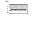
- FIG. 1 is a schematic cross-sectional view showing an example of the inorganic layer light emitting device of the present invention.
- the inorganic layer light emitting device shown in FIG. 1 is an inorganic layer light emitting device comprising a light emitting layer 50 containing a phosphor made of an inorganic material; and 30 or more metal-based particles 20 arranged two-dimensionally apart from each other. It includes a metal-based particle assembly layer that is a layer (film) made of particle assemblies arranged in the element.
- the inorganic layer light emitting device of the present invention can be obtained by laminating the above constituent layers on the substrate 10 in the same manner as a normal light emitting device.
- the light emitting layer 50 emits light by irradiating light of a predetermined wavelength that can excite the light emitting layer 50.
- electrodes are formed above and below the light emitting layer, for example, as in the inorganic LED elements shown in FIGS. 2 and 3 below. It is also possible to emit light by being electrically driven, that is, by generating excitons in the light emitting layer by hole injection and electron injection from the positive electrode and the negative electrode.
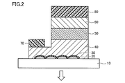
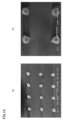
- FIG. 2 is a schematic cross-sectional view showing an example of the inorganic LED element according to the present invention, and shows an example of the structure of the inorganic LED element by electric drive.
- the inorganic LED element shown in FIG. 2 is a blue LED configured to extract light from the substrate 10 side (the arrow in the figure indicates the light extraction direction.
- the outer surface of the substrate 10 is the light extraction surface).
- a metal-based particle assembly layer in which 30 or more metal-based particles 20 are two-dimensionally arranged apart from each other and are laminated on the surface of the substrate 10 on the light-emitting layer side; on the metal-based particle assembly layer Insulating layer 30 to be laminated; n-type clad layer 40 made of n-GaN laminated on insulating layer 30; Light-emitting layer 50 made of InGaN / GaN laminated on n-type clad layer 40; P-type cladding layer 60 made of p-GaN to be laminated; first electrode 70 (negative electrode) disposed on the exposed surface of n-type cladding layer 40 formed by etching or the like; and laminated on p-type cladding layer 60 Second electrode 0 including the (positive electrode).
- the metal-based particle assembly layer is directly laminated (supported) on the substrate 10.
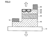
- FIG. 3 is a schematic cross-sectional view showing another example of the inorganic LED element according to the present invention, and shows an example of the structure of the inorganic LED element by electric drive as in FIG.
- the inorganic LED element shown in FIG. 3 is a blue LED having a configuration capable of extracting light from the front and back surfaces of the element (the arrow in the figure indicates the light extraction direction), and a p-type cladding serving as a light extraction surface.
- the metal-based particle assembly layer is disposed along the outer surface of the layer 60 (the surface opposite to the light emitting layer 50).
- the metal-based particle assembly layer is not limited to the examples shown in FIGS. 1 to 3, and can be disposed at any position in the inorganic layer light-emitting element, but is disposed closer to the light extraction surface than the light-emitting layer 50. Is preferable, and it is more preferable to arrange in the vicinity of the light extraction surface. As described above, in the present invention, the action range of plasmon resonance by the metal-based particle assembly layer can be remarkably extended, so that a position near the light extraction surface away from the light emitting layer 50 while ensuring a high light emission enhancing effect. It is possible to dispose a metal-based particle assembly layer on the surface.
- Arranging the metal-based particle assembly layer in the inorganic layer light-emitting element since the fluorescence lifetime is shortened by receiving the plasmon enhancement of the light-emitting layer, and the time during which the phosphor is in an excited state can be shortened. This is also advantageous for suppressing deterioration of the light emitter.
- the metal-based particle assembly layer is directly laminated (supported) on the substrate 10, and as a laminate of such a metal-based particle assembly layer and the substrate 10, A metal-based particle assembly layer laminated substrate that can be produced by the above-described method can be preferably used.
- the metal-based particle assembly layer can be laminated by, for example, growing on the insulating layer 30 formed on the p-type cladding layer 60 by the method described above.
- the substrate 10 may be made of any material including materials conventionally used for substrates of inorganic layer light-emitting elements, but particularly when the metal-based particle assembly layer is directly laminated on the substrate 10. From the viewpoint of ensuring non-conductivity of the metal-based particle assembly layer, it is preferable to use a non-conductive substrate.
- a non-conductive substrate glass, sapphire, other various inorganic insulating materials (SiO 2 , ZrO 2 , mica, etc.) and various plastic materials can be used.
- the substrate 10 preferably has translucency, and more preferably is optically transparent.
- the inorganic layer light emitting device of the present invention is interposed between the light emitting layer 50 and the metal-based particle assembly layer, more specifically, a metal-based particle assembly layer. It is preferable to further include an insulating layer 30 that covers the surface of each of the metal-based particles 20 constituting the structure. Such an insulating layer 30 can ensure the non-conductivity (non-conductivity between metal-based particles) of the metal-based particle assembly layer described above, and the metal-based particle assembly layer and other layers adjacent thereto. Can be electrically insulated.
- the inorganic layer light-emitting element current flows through each layer constituting the element, but if current flows through the metal-based particle assembly layer, the light emission enhancement effect by plasmon resonance may not be sufficiently obtained.
- the insulating layer 30 that caps the metal-based particle assembly layer it is possible to achieve electrical insulation between the metal-based particle assembly layer and another layer adjacent to the metal-based particle assembly layer. It is possible to prevent the current from being injected into the metal-based particles constituting the layer.
- the material constituting the insulating layer 30 is not particularly limited as long as it has good insulating properties.
- SiO 2 or Si 3 N 4 etc. can be used.
- the thickness of the insulating layer 30 is not particularly limited as long as desired insulating properties are ensured. However, as described later, the closer the distance between the light emitting layer 50 and the metal-based particle assembly layer is, the more preferable it is. It is better that the thickness is as thin as possible.
- the n-type clad layer 40, the light emitting layer 50, the p-type clad layer 60, the first electrode 70, and the second electrode 80 are not limited to those exemplified above, and can be made of a conventionally known material in this field. Moreover, those thicknesses may be the thickness that the inorganic layer light emitting element usually has. The light emitter and the thickness of the inorganic material constituting the light emitting layer 50 are selected according to the desired emission wavelength.
- Examples of light emitters include GaAsP, GaP, InGaN, InAlGaN, ZnCdSe, GaAlAs, InGaAlP and the like for inorganic LED elements, and ZnS: Mn, for example, JP-A-8-134440 for inorganic EL elements. Or the rare earth-added alkaline earth thioaluminate phosphor described in the above.
- the n-type cladding layer 40, the light emitting layer 50, and the p-type cladding layer 60 can be formed by metal organic chemical vapor deposition (MOCVD method), and the first electrode 70 and the second electrode 80 can be formed by vapor deposition.
- MOCVD method metal organic chemical vapor deposition
- the thickness of the light emitting layer 50 is usually 1 nm or more, and in the case of a multiple quantum well structure, the thickness can be 10 nm or more, further about 100 nm or more, but according to the present invention, strong plasmon resonance is exhibited.
- the metal-based particle assembly layer in which the plasmon resonance operating range (the range in which the plasmon enhances) is significantly extended is provided, the entire luminescent layer 50 is simultaneously enhanced even when the luminescent layer 50 is thick. Accordingly, the light emission efficiency of the inorganic layer light emitting element can be remarkably improved.
- the distance between the light emitting layer 50 and the metal-based particle assembly layer is not particularly limited.
- the metal-based particle assembly layer is disposed at a position away from the light emitting layer 50 by, for example, 10 nm, further several tens of nm (for example, more than 20 nm, 30 nm, or 40 nm), and even several hundred nm, plasmon An enhancement effect due to resonance can be obtained.
- the photoluminescence quantum yield (emitted) of the light emitting body that constitutes the light emitting layer 50 can be 1.5 times or more, or even 3 times or more, as compared to a reference inorganic layer light emitting device not having a metal particle aggregate layer.
- the distance between the light emitting layer 50 and the metal-based particle assembly layer is preferably 100 nm or less, more preferably 20 nm or less, and even more preferably 10 nm or less.
- the inorganic layer light emitting device of the present invention may further include other layers that may be included in a conventional inorganic layer light emitting device (not shown) such as a buffer layer and a current diffusion layer.
- the maximum wavelength of the plasmon peak of the metal-based particle assembly layer is preferably equal to or close to the emission wavelength of the light emitted from the light emitting layer 50. Thereby, the light emission enhancement effect by plasmon resonance can be heightened more effectively.
- the maximum wavelength of the plasmon peak of the metal-based particle assembly layer can be controlled by adjusting the metal species, average particle diameter, average height, aspect ratio, and / or average interparticle distance of the metal-based particles constituting the metal-based particle assembly layer.
- FIG. 4 is an SEM image when the metal-based particle assembly layer in the obtained metal-based particle assembly layer laminated substrate is viewed from directly above.
- FIG. 4A is an enlarged image on a 10000 times scale
- FIG. 4B is an enlarged image on a 50000 times scale.
- FIG. 5 is an AFM image showing the metal-based particle assembly layer in the obtained metal-based particle assembly layer laminated substrate.
- VN-8010 manufactured by Keyence Corporation was used (the same applies hereinafter).
- the size of the image shown in FIG. 5 is 5 ⁇ m ⁇ 5 ⁇ m.
- the average particle diameter based on the above definition of the silver particles constituting the metal-based particle assembly layer of this production example was determined to be 335 nm, and the average interparticle distance was 16.7 nm.
- the average height was determined to be 96.2 nm. From these, the aspect ratio (average particle diameter / average height) of the silver particles is calculated to be 3.48, and it can be seen from the acquired image that the silver particles have a flat shape. Furthermore, it can be seen from the SEM image that the metal-based particle assembly layer of this production example has about 6.25 ⁇ 10 10 (about 25 particles / ⁇ m 2 ) silver particles.
- the conductivity was confirmed by connecting a tester [Multimeter (“E2378A” manufactured by Hewlett-Packard Company)] to the surface of the metal-based particle assembly layer in the obtained metal-based particle assembly layer laminated substrate. It was confirmed that it does not have.
- a silver nanoparticle aqueous dispersion (manufactured by Mitsubishi Paper Industries, Ltd., silver nanoparticle concentration: 25% by weight) was diluted with pure water so that the silver nanoparticle concentration was 2% by weight. Next, 1% by volume of a surfactant was added to the silver nanoparticle aqueous dispersion and stirred well, then 80% by volume of acetone was added to the obtained silver nanoparticle aqueous dispersion, Was sufficiently stirred to prepare a silver nanoparticle coating solution.
- the silver nanoparticle coating solution was spin-coated at 1000 rpm on a 1 mm thick soda glass substrate whose surface was wiped with acetone with a square of 5 cm on one side, and then left in the air for 1 minute, and then 550 ° C. Baking for 40 seconds in an electric furnace.
- the above-mentioned silver nanoparticle coating solution is again spin-coated at 1000 rpm on the formed silver nanoparticle layer, and then left in the air for 1 minute, and then baked in an electric furnace at 550 ° C. for 40 seconds.
- a metal-based particle assembly layer laminated substrate was obtained.
- FIG. 6 is an SEM image when the metal-based particle assembly layer in the obtained metal-based particle assembly layer laminated substrate is viewed from directly above.
- FIG. 6A is an enlarged image on a 10000 times scale
- FIG. 6B is an enlarged image on a 50000 times scale.
- FIG. 7 is an AFM image showing the metal-based particle assembly layer in the obtained metal-based particle assembly layer laminated substrate. The size of the image shown in FIG. 7 is 5 ⁇ m ⁇ 5 ⁇ m.
- the average particle diameter based on the above definition of the silver particles constituting the metal-based particle assembly layer of this production example was determined to be 293 nm and the average interparticle distance was 107.8 nm. Further, the average height was determined to be 93.0 nm from the AFM image shown in FIG. From these, the aspect ratio (average particle diameter / average height) of the silver particles is calculated to be 3.15, and it can be seen from the acquired image that the silver particles have a flat shape. Furthermore, it can be seen from the SEM image that the metal-based particle assembly layer of this production example has about 3.13 ⁇ 10 10 (about 12.5 particles / ⁇ m 2 ) silver particles.
- the conductivity was confirmed by connecting a tester [Multimeter (“E2378A” manufactured by Hewlett-Packard Company)] to the surface of the metal-based particle assembly layer in the obtained metal-based particle assembly layer laminated substrate. It was confirmed that it does not have.
- the metal-based particle assembly layer laminated substrate of Comparative Production Example 1 has substantially the same particle shape, aspect ratio, and average interparticle distance as Production Example 1 except that the average height of the metal-based particles is about 10 nm.
- the metal-based particle assembly layer laminated substrate of Comparative Production Example 2 has substantially the same particle shape, aspect ratio, and average interparticle distance as Production Example 1 except that the average height of the metal-based particles is about 30 nm. there were.
- a silver nanoparticle aqueous dispersion (manufactured by Mitsubishi Paper Industries Co., Ltd., silver nanoparticle concentration: 25 wt%) was diluted with pure water so that the silver nanoparticle concentration was 6 wt%.
- 1% by volume of a surfactant was added to the silver nanoparticle aqueous dispersion and stirred well, and then 80% by volume of acetone was added to the obtained silver nanoparticle aqueous dispersion. was sufficiently stirred to prepare a silver nanoparticle coating solution.
- the silver nanoparticle coating solution was spin-coated at 1500 rpm on a 1 mm thick soda glass substrate whose surface was wiped with acetone with a square of 5 cm on one side, and then left in the air for 1 minute, and then 550 ° C. Firing for 5 minutes in an electric furnace yielded a metal-based particle assembly layer laminated substrate.
- FIG. 8 is a SEM image of the metal-based particle assembly layer in the metal-based particle assembly layer laminated substrate obtained in Comparative Production Example 3 when viewed from directly above, and is an enlarged image of 10000 times scale.
- FIG. 9 is an AFM image showing the metal-based particle assembly layer in the metal-based particle assembly layer laminated substrate obtained in Comparative Production Example 3. The size of the image shown in FIG. 9 is 5 ⁇ m ⁇ 5 ⁇ m.
- the average particle diameter based on the above definition of the silver particles constituting the metal-based particle assembly layer of Comparative Production Example 3 was determined to be 278 nm and the average interparticle distance was 195.5 nm.
- the average height was determined to be 99.5 nm. From these, the aspect ratio (average particle diameter / average height) of the silver particles is calculated to be 2.79, and it can be seen from the acquired image that the silver particles have a flat shape. Furthermore, it can be seen from the SEM image that the metal-based particle assembly layer of Comparative Production Example 3 has about 2.18 ⁇ 10 10 (about 8.72 particles / ⁇ m 2 ) silver particles.
- FIG. 10 is an absorption spectrum measured by an absorptiometry of the metal-based particle assembly layer laminated substrate obtained in Production Example 1 and Comparative Production Examples 1-2.
- Non-patent literature K. Lance Kelly, et al., "The Optical Properties of Metal Nanoparticles: The Influence of Size, Shape, and Dielectric Environment", The Journal of Physical Chemistry B, 2003, 107, 668)
- the flat silver particles as in Production Example 1 generally have a plasmon peak around 550 nm when the average particle size is 200 nm and around 650 nm when the average particle size is 300 nm. (All are silver particles alone).
- the metal-based particle assembly layer laminated substrate of Production Example 1 has a visible light region as shown in FIG. 10 even though the average particle diameter of silver particles constituting the metal-based particle assembly layer laminated substrate is about 300 nm (335 nm). It can be seen that the maximum wavelength of the plasmon peak on the longest wavelength side is shifted to the short wavelength side in the vicinity of about 450 nm. This phenomenon can occur when the silver particles are large particles having the predetermined shape and are arranged very densely at the predetermined average interparticle distance as in Production Example 1. Such a phenomenon is difficult to reasonably interpret only by the presence of plasmon interaction occurring in each particle due to the proximity of the particles.
- the maximum wavelength of the plasmon peak depends on the average particle diameter of the metal-based particles.
- Comparative Production Examples 1 and 2 have a plasmon peak considerably longer than Production Example 1 due to the small average particle size, and the maximum wavelengths are about 510 nm and about 470 nm, respectively. .
- the absorbance at the maximum wavelength of the plasmon peak on the longest wavelength side in the visible light region is about 1.9, which is extremely higher than Comparative Production Examples 1 and 2, and from this, the metal system of Production Example 1 It can be seen that the particle assembly layer exhibits extremely strong plasmon resonance.
- FIG. 11 shows an absorption spectrum measured by the absorptiometry of the metal-based particle assembly layer laminated substrate obtained in Production Example 2.
- the maximum wavelength of the plasmon peak on the longest wavelength side in the visible light region was 488 nm.
- the absorption spectra shown in FIGS. 10 and 11 are on the back side of the metal-based particle assembly layer laminated substrate (on the side opposite to the metal-based particle assembly layer) and from the direction perpendicular to the substrate surface. It is a substrate having the same thickness and material as the substrate of the metal particle assembly film laminated substrate, and the intensity I of transmitted light in all directions irradiated with incident light in the visible light region and transmitted to the metal particle assembly layer side. Then, the same incident light is irradiated from the direction perpendicular to the surface of the substrate on which the metal-based particle assembly film is not stacked, and the transmitted light intensity I 0 in all directions transmitted from the opposite side of the incident surface is It was obtained by measuring using an integrating sphere spectrophotometer.
- a substrate on which a reference metal-based particle assembly was laminated was produced.
- a resist (ZEP520A manufactured by Nippon Zeon Co., Ltd.) was spin-coated on approximately the entire surface of a soda glass substrate 100 having a length of 5 cm and a width of 5 cm (FIG. 12A).
- the thickness of the resist 400 was about 120 nm.
- a circular opening 401 was formed in the resist 400 by electron beam lithography (FIG. 12B).
- the diameter of the circular opening 401 was about 350 nm.
- the distance between the centers of the adjacent circular openings 401 was set to about 1500 nm.
- a silver film 201 was deposited on the resist 400 having the circular opening 401 by a vacuum deposition method (FIG. 12C).
- the film thickness of the silver film 201 was about 100 nm.
- the substrate having the silver film 201 is dipped in NMP (N-methyl-2-pyrrolidone, manufactured by Tokyo Chemical Industry Co., Ltd.), and left on the ultrasonic device for 1 minute at room temperature to form a film on the resist 400 and the resist 400.
- the thus-prepared silver film 201 was peeled off, and only the silver film 201 (silver particles) in the circular opening 401 remained on the soda glass substrate 100 to obtain a reference metal-based particle assembly layer laminated substrate (FIG. 12). (D)).
- FIG. 13 is an SEM image when the reference metal-based particle assembly layer in the obtained reference metal-based particle assembly layer laminated substrate is viewed from directly above.
- FIG. 13A is an enlarged image of 20000 times scale
- FIG. 13B is an enlarged image of 50000 times scale. From the SEM image shown in FIG. 13, the average particle diameter based on the above definition of the silver particles constituting the reference metal-based particle assembly layer was determined to be 333 nm, and the average interparticle distance was 1264 nm. The average height was determined to be 105.9 nm from the separately acquired AFM image. Further, from the SEM image, it was found that the reference metal-based particle aggregate had about 62500 silver particles.
- the absorption spectrum of the metal-based particle assembly layer laminated substrate of Production Example 1 was measured by the measurement method using the objective lens (100 times) of the microscope described above. Specifically, referring to FIG. 14, the metal-based particle assembly film laminated substrate 500 is visible on the substrate 501 side (the side opposite to the metal-based particle assembly layer 502) from a direction perpendicular to the substrate surface. Incident light in the light region was irradiated. Then, the transmitted light that has been transmitted to the metal-based particle assembly layer 502 side and has reached 100 times the objective lens 600 is condensed by the objective lens 600, and this condensed light is detected by the spectrophotometer 700, and the absorption spectrum is obtained. Got.
- the spectrophotometer 700 was an ultraviolet-visible spectrophotometer “MCPD-3000” manufactured by Otsuka Electronics Co., Ltd., and the objective lens 600 was a “BD Plan 100 / 0.80 ELWD” manufactured by Nikon.
- the results are shown in FIG.
- the maximum wavelength of the plasmon peak on the longest wavelength side in the visible light region was about 450 nm as in the absorption spectrum of FIG.
- the absorption spectrum of the reference metal-based particle assembly layer laminated substrate was measured by the same measurement method using an objective lens of a microscope, the maximum wavelength of the peak on the longest wavelength side in the visible light region was 654 nm. It was.
- the peak maximum wavelength on the longest wavelength side in the visible light region is blue-shifted by about 200 nm compared to the reference metal-based particle assembly layer multilayer substrate.
- the metal-based particle assembly layer multilayer substrate of Production Example 1 has an absorbance at the maximum wavelength of the peak at the longest wavelength side in the visible light region of 1.744 (FIG. 15), and the reference metal-based particle assembly layer multilayer substrate was 0.033.
- the absorbance / coverage was calculated by dividing the absorbance obtained from the absorption spectrum by the coverage of the substrate surface with metal particles, which is a parameter corresponding to the number of metal particles.
- the absorbance / coverage of the metal-based particle assembly layer multilayer substrate of Production Example 1 is 2.04 (coverage 85.3%), and the absorbance / coverage of the reference metal-based particle assembly layer multilayer substrate is 0.84. (Coverage 3.9%).
- 16 and 17 are absorption spectra of the metal-based particle assembly layer laminated substrate of Production Example 2 and Comparative Production Example 3 by a measurement method using an objective lens (100 times) of a microscope.
- the metal-based particle assembly layer laminated substrate obtained in Comparative Production Example 3 had a peak maximum wavelength on the longest wavelength side in the visible light region of 611 nm. This maximum wavelength is almost the same as the maximum wavelength of the reference metal-based particle assembly film laminated substrate corresponding to the metal-based particle assembly film-laminated substrate of Comparative Production Example 3, and therefore the metal-based particle assembly of Comparative Production Example 3
- the membrane shows little blue shift.
- the absorbance at the maximum wavelength of the peak on the longest wavelength side in the visible light region obtained from the absorption spectrum of FIG. 17 is 0.444, and the coverage of the substrate surface with metal-based particles is 53.2%. Absorbance / coverage is calculated as 0.83. This absorbance / coverage is smaller than that of the reference metal-based particle assembly layer laminated substrate.
- the metal-based particle assembly of Production Example 2 Since the metal-based particle assembly of Production Example 2 has a larger average particle size than the metal-based particle assembly of Comparative Production Example 3, the plasmon peak of the metal-based particle assembly of Production Example 2 is compared. Compared to Production Example 3, it appears reasonably from the Mie scattering theory that it appears on the longer wavelength side. However, actually, the plasmon peak of the metal-based particle aggregate of Production Example 2 appeared on the short wavelength side as much as 100 nm or more as compared with Comparative Production Example 3. From this, it is rational that the metal-based particle assembly of Production Example 2 has the maximum wavelength of the plasmon peak shifted to the short wavelength side in the range of 30 to 500 nm as compared to the reference metal-based particle assembly. Is suggested.
- Example 1 By growing silver particles under substantially the same conditions as in Production Example 1, the same metal-based particle assembly layer as in Production Example 1 was formed on a 0.5 mm thick soda glass substrate. This metal-based particle assembly layer had the same particle shape and average interparticle distance as in Production Example 1 except that the average height of the metal-based particles was 57.3 nm. After forming the metal-based particle assembly layer, an SOG solution was immediately spin-coated on the metal-based particle assembly layer to provide an insulating layer having an average thickness of 10 nm.
- the “average thickness” of the insulating layer means the average thickness of the insulating layer formed on the metal-based particle assembly layer having surface irregularities, and when the SOG solution is directly spin-coated on the soda glass substrate. The thickness was measured (the same applies to the following examples and comparative examples). When the average thickness is a relatively small value, an insulating layer is formed only in the valley portion of the metal-based particle assembly layer, and the entire outermost surface of the metal-based particle assembly layer may not be covered.
- an aqueous dispersion of a fluorescent paint “Lumilite Nano RY202” sold by Sinloi Co., Ltd., pure water and isopropyl alcohol is used at a volume ratio of 2
- the inorganic light emitting layer solution mixed at a ratio of 2: 1 was spin-coated at 1500 rpm to form an inorganic light emitting layer to obtain an inorganic layer light emitting device.
- Example 2 An inorganic layer light emitting device was produced in the same manner as in Example 1 except that the average thickness of the insulating layer was 30 nm.
- Example 3 An inorganic layer light emitting device was produced in the same manner as in Example 1 except that the average thickness of the insulating layer was 80 nm.
- Example 4 An inorganic layer light emitting device was produced in the same manner as in Example 1 except that the average thickness of the insulating layer was 150 nm.
- Example 2 The same inorganic light emitting layer solution as used in Example 1 was directly spin-coated at 1500 rpm on a 0.5 mm thick soda glass substrate to form an inorganic light emitting layer to obtain an inorganic layer light emitting device.
- the degree of light emission enhancement was evaluated as follows. That is, with reference to FIG. 18 showing a measurement system of the emission spectrum of the inorganic layer light-emitting element and FIG. 1 which is a schematic sectional view of the inorganic layer light-emitting element, the inorganic light-emitting layer is provided on the inorganic light-emitting layer 50 side of the inorganic layer light-emitting element 1.
- the inorganic light emitting device 1 was caused to emit light by irradiating the excitation light 3 from a direction perpendicular to the surface of 50.
- the excitation light source 4 that emits the excitation light 3 is a UV-LED (UV-LED 375-14S manufactured by South Walker, excitation light wavelength: 375 nm), and the light emitted from the excitation light source 4 is condensed by the lens 5 and the excitation light 3 And this was irradiated.
- a wavelength cut filter 8 (sigma light) that condenses the light emission 6 from the inorganic light emitting element 1 emitted in the direction of 40 ° with respect to the optical axis of the excitation light 3 by the lens 7 and cuts the light having the wavelength of the excitation light 3.
- a spectrophotometer 9 MCPD-3000, manufactured by Otsuka Electronics Co., Ltd.
- the peak value in the emission wavelength region was determined for the detected emission spectrum.
- the value obtained by dividing the peak value obtained from the emission spectra measured for the inorganic light-emitting elements of Examples 1 to 4 and Comparative Examples 1 to 4 by the peak value obtained from the emission spectrum measured for the inorganic light-emitting element of the control example was “luminescence”.
- a graph with the “magnification factor” as the vertical axis is shown in FIG.
- 1 inorganic light emitting element 3 excitation light, 4 excitation light source, 5, 7 lens, 6 light emission from inorganic light emitting element, 8 wavelength cut filter, 9 spectrometer, 10 substrate, 20 metal particles, 30 insulating layer, 40 n Type cladding layer, 50 light emitting layer, 60 p-type cladding layer, 70 first electrode, 80 second electrode, 100 soda glass substrate, 201 silver film, 400 resist, 401 circular opening, 500 metal-based particle assembly layer laminated substrate 501 substrate, 502 metal-based particle assembly layer, 600 objective lens, 700 spectrophotometer.
Landscapes
- Engineering & Computer Science (AREA)
- Microelectronics & Electronic Packaging (AREA)
- Manufacturing & Machinery (AREA)
- Computer Hardware Design (AREA)
- Power Engineering (AREA)
- Electroluminescent Light Sources (AREA)
- Led Devices (AREA)
Abstract
Priority Applications (2)
| Application Number | Priority Date | Filing Date | Title |
|---|---|---|---|
| KR1020147029511A KR20140148430A (ko) | 2012-03-27 | 2013-03-13 | 무기층 발광 소자 |
| US14/386,104 US9263630B2 (en) | 2012-03-27 | 2013-03-13 | Inorganic layer light-emitting device |
Applications Claiming Priority (2)
| Application Number | Priority Date | Filing Date | Title |
|---|---|---|---|
| JP2012071685 | 2012-03-27 | ||
| JP2012-071685 | 2012-03-27 |
Publications (1)
| Publication Number | Publication Date |
|---|---|
| WO2013146268A1 true WO2013146268A1 (fr) | 2013-10-03 |
Family
ID=49259532
Family Applications (1)
| Application Number | Title | Priority Date | Filing Date |
|---|---|---|---|
| PCT/JP2013/057007 WO2013146268A1 (fr) | 2012-03-27 | 2013-03-13 | Élément électroluminescent à couche inorganique |
Country Status (4)
| Country | Link |
|---|---|
| US (1) | US9263630B2 (fr) |
| JP (1) | JPWO2013146268A1 (fr) |
| KR (1) | KR20140148430A (fr) |
| WO (1) | WO2013146268A1 (fr) |
Families Citing this family (3)
| Publication number | Priority date | Publication date | Assignee | Title |
|---|---|---|---|---|
| CN104362232B (zh) * | 2014-10-28 | 2019-03-29 | 天津三安光电有限公司 | 一种发光二极管 |
| CN110444641B (zh) * | 2019-08-13 | 2020-05-05 | 黄山博蓝特半导体科技有限公司 | 一种高亮度图形化复合衬底及其制作方法 |
| CN110429099B (zh) * | 2019-08-13 | 2020-05-05 | 黄山博蓝特半导体科技有限公司 | 一种高亮度复合衬底的制作方法 |
Citations (6)
| Publication number | Priority date | Publication date | Assignee | Title |
|---|---|---|---|---|
| JP2010238775A (ja) * | 2009-03-30 | 2010-10-21 | Fujifilm Corp | 発光素子 |
| WO2011027830A1 (fr) * | 2009-09-07 | 2011-03-10 | 国立大学法人北海道大学 | Dispositif de conversion photoélectrique, dispositif de détection de lumière et procédé de détection de lumière |
| WO2012133776A1 (fr) * | 2011-03-31 | 2012-10-04 | 住友化学株式会社 | Agrégat particulaire métallique |
| WO2012133779A1 (fr) * | 2011-03-31 | 2012-10-04 | 住友化学株式会社 | Élément électroluminescent organique |
| WO2012133778A1 (fr) * | 2011-03-31 | 2012-10-04 | 住友化学株式会社 | Agrégat particulaire métallique |
| WO2012133777A1 (fr) * | 2011-03-31 | 2012-10-04 | 住友化学株式会社 | Agrégat particulaire métallique |
Family Cites Families (33)
| Publication number | Priority date | Publication date | Assignee | Title |
|---|---|---|---|---|
| US6074575A (en) | 1994-11-14 | 2000-06-13 | Mitsui Mining & Smelting Co., Ltd. | Thin film electro-luminescence device |
| JPH08134440A (ja) | 1994-11-14 | 1996-05-28 | Mitsui Mining & Smelting Co Ltd | 薄膜エレクトロルミネッセンス素子 |
| AT403961B (de) | 1995-03-17 | 1998-07-27 | Avl Verbrennungskraft Messtech | Optochemisches messsystem mit einem fluoreszenzsensor |
| TW595259B (en) | 2003-01-28 | 2004-06-21 | Ind Tech Res Inst | Organic electroluminescent device |
| CN1527648A (zh) | 2003-03-07 | 2004-09-08 | 财团法人工业技术研究院 | 有机电激发光装置 |
| US7420156B2 (en) | 2003-08-06 | 2008-09-02 | University Of Pittsburgh | Metal nanowire based bandpass filter arrays in the optical frequency range |
| KR20060130543A (ko) | 2003-08-06 | 2006-12-19 | 유니버시티 오브 피츠버그 오브 더 커먼웰쓰 시스템 오브 하이어 에듀케이션 | 표면 플라즈몬-강화 나노-광 소자 및 그의 제조 방법 |
| FR2860872A1 (fr) | 2003-10-09 | 2005-04-15 | Commissariat Energie Atomique | Micro-capteurs et nano-capteurs d'especes chimiques et biologiques a plasmons de surface |
| US8592680B2 (en) | 2004-08-11 | 2013-11-26 | The Trustees Of Princeton University | Organic photosensitive devices |
| WO2006085515A1 (fr) | 2005-02-09 | 2006-08-17 | Kyoto University | Dispositif optique de controle de la reflexion |
| US7403287B2 (en) | 2005-06-08 | 2008-07-22 | Canon Kabushiki Kaisha | Sensing element used in sensing device for sensing target substance in specimen by using plasmon resonance |
| JP2007017432A (ja) | 2005-06-08 | 2007-01-25 | Canon Inc | プラズモン共鳴を利用して検体中の標的物質を検知するための検知装置に用いられる検知素子及びその製造方法 |
| FR2891279B1 (fr) | 2005-09-27 | 2007-12-14 | Centre Nat Rech Scient | Nouvelles puces pour la detection par le plasmon de surface (spr) |
| JP4825974B2 (ja) | 2005-11-17 | 2011-11-30 | 国立大学法人京都大学 | 蛍光増強素子、蛍光素子、及び蛍光増強方法 |
| JP2007165284A (ja) | 2005-11-18 | 2007-06-28 | Seiko Instruments Inc | エレクトロルミネッセンス素子及びこれを用いた表示装置 |
| JP2007335222A (ja) | 2006-06-15 | 2007-12-27 | Ipb:Kk | 光電極、及びそれを用いた色素増感太陽電池、並びにその製造方法 |
| WO2008028130A1 (fr) | 2006-09-01 | 2008-03-06 | William Marsh Rice University | Compositions pour spectres d'absorption infrarouge exaltés de surface et procédés d'utilisation de celles-ci |
| EP2092308A1 (fr) | 2006-12-05 | 2009-08-26 | Yeda Research And Development Company Limited | Dispositif et procédé pour la détection optique localisée d'un plasmon |
| WO2008082569A1 (fr) | 2006-12-29 | 2008-07-10 | Nanolambda, Inc. | Nanostructure à gaufrage métallique sélective en longueur d'onde |
| JP2008214363A (ja) | 2007-02-28 | 2008-09-18 | Canon Inc | ナノ粒子発光材料、これを用いた電界発光素子及びインク組成物、並びに表示装置 |
| JP2008243669A (ja) | 2007-03-28 | 2008-10-09 | Toyota Central R&D Labs Inc | 有機電界発光素子 |
| KR101239904B1 (ko) | 2007-08-27 | 2013-03-06 | 파나소닉 주식회사 | 유기 이엘 소자 |
| JP4597175B2 (ja) | 2007-09-21 | 2010-12-15 | 株式会社日立ハイテクノロジーズ | 標的物質を検出するための分析装置、又は分析方法、若しくはこれら分析装置及び分析方法に用いるデバイス |
| US8115920B2 (en) | 2007-11-14 | 2012-02-14 | 3M Innovative Properties Company | Method of making microarrays |
| US8097295B2 (en) | 2008-02-27 | 2012-01-17 | The University Of Utah Research Foundation | Method of making nanoparticles by electroless plating |
| US8058609B2 (en) | 2008-09-30 | 2011-11-15 | The Invention Science Fund I, Llc | Beam power with multipoint broadcast |
| US20100126567A1 (en) | 2008-11-21 | 2010-05-27 | Lightwave Power, Inc. | Surface plasmon energy conversion device |
| WO2010081088A1 (fr) | 2009-01-09 | 2010-07-15 | Trustees Of Boston University | Substrat sers d’ingénierie utilisant des réseaux d’amas de nanoparticules présentant une exaltation du signal multi-échelle |
| JP5312145B2 (ja) | 2009-03-30 | 2013-10-09 | ユー・ディー・シー アイルランド リミテッド | エレクトロルミネッセンス素子 |
| US8259381B2 (en) | 2009-06-05 | 2012-09-04 | Exelis Inc. | Phase-change materials and optical limiting devices utilizing phase-change materials |
| CN102918651A (zh) | 2010-04-02 | 2013-02-06 | 株式会社东芝 | 光电转换元件及其制造方法 |
| JP2012074569A (ja) | 2010-09-29 | 2012-04-12 | Jx Nippon Oil & Energy Corp | 光電変換素子 |
| JP6373552B2 (ja) | 2011-10-26 | 2018-08-15 | 住友化学株式会社 | 光電変換素子 |
-
2013
- 2013-03-13 WO PCT/JP2013/057007 patent/WO2013146268A1/fr active Application Filing
- 2013-03-13 JP JP2014507649A patent/JPWO2013146268A1/ja active Pending
- 2013-03-13 KR KR1020147029511A patent/KR20140148430A/ko not_active Application Discontinuation
- 2013-03-13 US US14/386,104 patent/US9263630B2/en not_active Expired - Fee Related
Patent Citations (6)
| Publication number | Priority date | Publication date | Assignee | Title |
|---|---|---|---|---|
| JP2010238775A (ja) * | 2009-03-30 | 2010-10-21 | Fujifilm Corp | 発光素子 |
| WO2011027830A1 (fr) * | 2009-09-07 | 2011-03-10 | 国立大学法人北海道大学 | Dispositif de conversion photoélectrique, dispositif de détection de lumière et procédé de détection de lumière |
| WO2012133776A1 (fr) * | 2011-03-31 | 2012-10-04 | 住友化学株式会社 | Agrégat particulaire métallique |
| WO2012133779A1 (fr) * | 2011-03-31 | 2012-10-04 | 住友化学株式会社 | Élément électroluminescent organique |
| WO2012133778A1 (fr) * | 2011-03-31 | 2012-10-04 | 住友化学株式会社 | Agrégat particulaire métallique |
| WO2012133777A1 (fr) * | 2011-03-31 | 2012-10-04 | 住友化学株式会社 | Agrégat particulaire métallique |
Non-Patent Citations (3)
| Title |
|---|
| GEORGE CHUMANOV ET AL.: "Unusual Extinction Spectra of Nanometer-Sized Silver Particles Arranged in Two-Dimensional Arrays", JOURNAL OF PHYSICAL CHEMISTRY, vol. 100, no. 13, 1996, pages 5166 - 5168, XP002056205, DOI: doi:10.1021/jp9536716 * |
| JIHA SUNG ET AL.: "Nanoparticle Spectroscopy: Plasmon Coupling in Finite-Sized Two- Dimensional Arrays of Cylindrical Silver Nanoparticles", JOURNAL OF PHYSICAL CHEMISTRY C, vol. 112, no. 11, 26 February 2008 (2008-02-26), pages 4091 - 4096 * |
| TOMOHIRO FUKUURA ET AL.: "Long Range Enhancement of Molecular Fluorescence by Closely Packed Submicro-scale Ag Islands", E- JOURNAL OF SURFACE SCIENCE AND NANOTECHNOLOGY, vol. 7, 23 May 2009 (2009-05-23), pages 653 - 659 * |
Also Published As
| Publication number | Publication date |
|---|---|
| US9263630B2 (en) | 2016-02-16 |
| KR20140148430A (ko) | 2014-12-31 |
| JPWO2013146268A1 (ja) | 2015-12-10 |
| US20150041842A1 (en) | 2015-02-12 |
Similar Documents
| Publication | Publication Date | Title |
|---|---|---|
| JP5969877B2 (ja) | 量子ドット発光素子 | |
| JP5979932B2 (ja) | 有機エレクトロルミネッセンス素子 | |
| JP6018774B2 (ja) | 金属系粒子集合体 | |
| JP6085095B2 (ja) | 光学素子 | |
| JP6018857B2 (ja) | 金属系粒子集合体 | |
| JP6373552B2 (ja) | 光電変換素子 | |
| JP6125758B2 (ja) | 光学素子 | |
| WO2013146268A1 (fr) | Élément électroluminescent à couche inorganique | |
| KR102002190B1 (ko) | 금속계 입자 집합체의 제조 방법 |
Legal Events
| Date | Code | Title | Description |
|---|---|---|---|
| 121 | Ep: the epo has been informed by wipo that ep was designated in this application |
Ref document number: 13768268 Country of ref document: EP Kind code of ref document: A1 |
|
| ENP | Entry into the national phase |
Ref document number: 2014507649 Country of ref document: JP Kind code of ref document: A |
|
| WWE | Wipo information: entry into national phase |
Ref document number: 14386104 Country of ref document: US |
|
| ENP | Entry into the national phase |
Ref document number: 20147029511 Country of ref document: KR Kind code of ref document: A |
|
| NENP | Non-entry into the national phase |
Ref country code: DE |
|
| 122 | Ep: pct application non-entry in european phase |
Ref document number: 13768268 Country of ref document: EP Kind code of ref document: A1 |