WO2013145616A1 - Method for manufacturing electrophotography member, and coating liquid - Google Patents
Method for manufacturing electrophotography member, and coating liquid Download PDFInfo
- Publication number
- WO2013145616A1 WO2013145616A1 PCT/JP2013/001779 JP2013001779W WO2013145616A1 WO 2013145616 A1 WO2013145616 A1 WO 2013145616A1 JP 2013001779 W JP2013001779 W JP 2013001779W WO 2013145616 A1 WO2013145616 A1 WO 2013145616A1
- Authority
- WO
- WIPO (PCT)
- Prior art keywords
- general formula
- group
- compound represented
- carbon atoms
- alkyl group
- Prior art date
Links
Images


Classifications
-
- C—CHEMISTRY; METALLURGY
- C09—DYES; PAINTS; POLISHES; NATURAL RESINS; ADHESIVES; COMPOSITIONS NOT OTHERWISE PROVIDED FOR; APPLICATIONS OF MATERIALS NOT OTHERWISE PROVIDED FOR
- C09D—COATING COMPOSITIONS, e.g. PAINTS, VARNISHES OR LACQUERS; FILLING PASTES; CHEMICAL PAINT OR INK REMOVERS; INKS; CORRECTING FLUIDS; WOODSTAINS; PASTES OR SOLIDS FOR COLOURING OR PRINTING; USE OF MATERIALS THEREFOR
- C09D183/00—Coating compositions based on macromolecular compounds obtained by reactions forming in the main chain of the macromolecule a linkage containing silicon, with or without sulfur, nitrogen, oxygen, or carbon only; Coating compositions based on derivatives of such polymers
- C09D183/04—Polysiloxanes
- C09D183/06—Polysiloxanes containing silicon bound to oxygen-containing groups
-
- G—PHYSICS
- G03—PHOTOGRAPHY; CINEMATOGRAPHY; ANALOGOUS TECHNIQUES USING WAVES OTHER THAN OPTICAL WAVES; ELECTROGRAPHY; HOLOGRAPHY
- G03G—ELECTROGRAPHY; ELECTROPHOTOGRAPHY; MAGNETOGRAPHY
- G03G15/00—Apparatus for electrographic processes using a charge pattern
- G03G15/02—Apparatus for electrographic processes using a charge pattern for laying down a uniform charge, e.g. for sensitising; Corona discharge devices
- G03G15/0208—Apparatus for electrographic processes using a charge pattern for laying down a uniform charge, e.g. for sensitising; Corona discharge devices by contact, friction or induction, e.g. liquid charging apparatus
- G03G15/0216—Apparatus for electrographic processes using a charge pattern for laying down a uniform charge, e.g. for sensitising; Corona discharge devices by contact, friction or induction, e.g. liquid charging apparatus by bringing a charging member into contact with the member to be charged, e.g. roller, brush chargers
- G03G15/0233—Structure, details of the charging member, e.g. chemical composition, surface properties
-
- G—PHYSICS
- G03—PHOTOGRAPHY; CINEMATOGRAPHY; ANALOGOUS TECHNIQUES USING WAVES OTHER THAN OPTICAL WAVES; ELECTROGRAPHY; HOLOGRAPHY
- G03G—ELECTROGRAPHY; ELECTROPHOTOGRAPHY; MAGNETOGRAPHY
- G03G15/00—Apparatus for electrographic processes using a charge pattern
- G03G15/06—Apparatus for electrographic processes using a charge pattern for developing
- G03G15/08—Apparatus for electrographic processes using a charge pattern for developing using a solid developer, e.g. powder developer
- G03G15/0806—Apparatus for electrographic processes using a charge pattern for developing using a solid developer, e.g. powder developer on a donor element, e.g. belt, roller
- G03G15/0818—Apparatus for electrographic processes using a charge pattern for developing using a solid developer, e.g. powder developer on a donor element, e.g. belt, roller characterised by the structure of the donor member, e.g. surface properties
-
- G—PHYSICS
- G03—PHOTOGRAPHY; CINEMATOGRAPHY; ANALOGOUS TECHNIQUES USING WAVES OTHER THAN OPTICAL WAVES; ELECTROGRAPHY; HOLOGRAPHY
- G03G—ELECTROGRAPHY; ELECTROPHOTOGRAPHY; MAGNETOGRAPHY
- G03G15/00—Apparatus for electrographic processes using a charge pattern
- G03G15/14—Apparatus for electrographic processes using a charge pattern for transferring a pattern to a second base
- G03G15/16—Apparatus for electrographic processes using a charge pattern for transferring a pattern to a second base of a toner pattern, e.g. a powder pattern, e.g. magnetic transfer
- G03G15/1605—Apparatus for electrographic processes using a charge pattern for transferring a pattern to a second base of a toner pattern, e.g. a powder pattern, e.g. magnetic transfer using at least one intermediate support
- G03G15/162—Apparatus for electrographic processes using a charge pattern for transferring a pattern to a second base of a toner pattern, e.g. a powder pattern, e.g. magnetic transfer using at least one intermediate support details of the the intermediate support, e.g. chemical composition
-
- G—PHYSICS
- G03—PHOTOGRAPHY; CINEMATOGRAPHY; ANALOGOUS TECHNIQUES USING WAVES OTHER THAN OPTICAL WAVES; ELECTROGRAPHY; HOLOGRAPHY
- G03G—ELECTROGRAPHY; ELECTROPHOTOGRAPHY; MAGNETOGRAPHY
- G03G15/00—Apparatus for electrographic processes using a charge pattern
- G03G15/14—Apparatus for electrographic processes using a charge pattern for transferring a pattern to a second base
- G03G15/16—Apparatus for electrographic processes using a charge pattern for transferring a pattern to a second base of a toner pattern, e.g. a powder pattern, e.g. magnetic transfer
- G03G15/1665—Apparatus for electrographic processes using a charge pattern for transferring a pattern to a second base of a toner pattern, e.g. a powder pattern, e.g. magnetic transfer by introducing the second base in the nip formed by the recording member and at least one transfer member, e.g. in combination with bias or heat
- G03G15/167—Apparatus for electrographic processes using a charge pattern for transferring a pattern to a second base of a toner pattern, e.g. a powder pattern, e.g. magnetic transfer by introducing the second base in the nip formed by the recording member and at least one transfer member, e.g. in combination with bias or heat at least one of the recording member or the transfer member being rotatable during the transfer
- G03G15/1685—Structure, details of the transfer member, e.g. chemical composition
-
- G—PHYSICS
- G03—PHOTOGRAPHY; CINEMATOGRAPHY; ANALOGOUS TECHNIQUES USING WAVES OTHER THAN OPTICAL WAVES; ELECTROGRAPHY; HOLOGRAPHY
- G03G—ELECTROGRAPHY; ELECTROPHOTOGRAPHY; MAGNETOGRAPHY
- G03G15/00—Apparatus for electrographic processes using a charge pattern
- G03G15/20—Apparatus for electrographic processes using a charge pattern for fixing, e.g. by using heat
- G03G15/2003—Apparatus for electrographic processes using a charge pattern for fixing, e.g. by using heat using heat
- G03G15/2014—Apparatus for electrographic processes using a charge pattern for fixing, e.g. by using heat using heat using contact heat
- G03G15/2053—Structural details of heat elements, e.g. structure of roller or belt, eddy current, induction heating
- G03G15/2057—Structural details of heat elements, e.g. structure of roller or belt, eddy current, induction heating relating to the chemical composition of the heat element and layers thereof
-
- G—PHYSICS
- G03—PHOTOGRAPHY; CINEMATOGRAPHY; ANALOGOUS TECHNIQUES USING WAVES OTHER THAN OPTICAL WAVES; ELECTROGRAPHY; HOLOGRAPHY
- G03G—ELECTROGRAPHY; ELECTROPHOTOGRAPHY; MAGNETOGRAPHY
- G03G15/00—Apparatus for electrographic processes using a charge pattern
- G03G15/20—Apparatus for electrographic processes using a charge pattern for fixing, e.g. by using heat
- G03G15/2003—Apparatus for electrographic processes using a charge pattern for fixing, e.g. by using heat using heat
- G03G15/2014—Apparatus for electrographic processes using a charge pattern for fixing, e.g. by using heat using heat using contact heat
- G03G15/206—Structural details or chemical composition of the pressure elements and layers thereof
-
- G—PHYSICS
- G03—PHOTOGRAPHY; CINEMATOGRAPHY; ANALOGOUS TECHNIQUES USING WAVES OTHER THAN OPTICAL WAVES; ELECTROGRAPHY; HOLOGRAPHY
- G03G—ELECTROGRAPHY; ELECTROPHOTOGRAPHY; MAGNETOGRAPHY
- G03G5/00—Recording members for original recording by exposure, e.g. to light, to heat, to electrons; Manufacture thereof; Selection of materials therefor
- G03G5/14—Inert intermediate or cover layers for charge-receiving layers
- G03G5/147—Cover layers
- G03G5/14704—Cover layers comprising inorganic material
-
- G—PHYSICS
- G03—PHOTOGRAPHY; CINEMATOGRAPHY; ANALOGOUS TECHNIQUES USING WAVES OTHER THAN OPTICAL WAVES; ELECTROGRAPHY; HOLOGRAPHY
- G03G—ELECTROGRAPHY; ELECTROPHOTOGRAPHY; MAGNETOGRAPHY
- G03G5/00—Recording members for original recording by exposure, e.g. to light, to heat, to electrons; Manufacture thereof; Selection of materials therefor
- G03G5/14—Inert intermediate or cover layers for charge-receiving layers
- G03G5/147—Cover layers
- G03G5/14708—Cover layers comprising organic material
- G03G5/14713—Macromolecular material
- G03G5/14747—Macromolecular material obtained otherwise than by reactions only involving carbon-to-carbon unsaturated bonds
- G03G5/14773—Polycondensates comprising silicon atoms in the main chain
-
- C—CHEMISTRY; METALLURGY
- C08—ORGANIC MACROMOLECULAR COMPOUNDS; THEIR PREPARATION OR CHEMICAL WORKING-UP; COMPOSITIONS BASED THEREON
- C08G—MACROMOLECULAR COMPOUNDS OBTAINED OTHERWISE THAN BY REACTIONS ONLY INVOLVING UNSATURATED CARBON-TO-CARBON BONDS
- C08G77/00—Macromolecular compounds obtained by reactions forming a linkage containing silicon with or without sulfur, nitrogen, oxygen or carbon in the main chain of the macromolecule
- C08G77/04—Polysiloxanes
- C08G77/14—Polysiloxanes containing silicon bound to oxygen-containing groups
-
- G—PHYSICS
- G03—PHOTOGRAPHY; CINEMATOGRAPHY; ANALOGOUS TECHNIQUES USING WAVES OTHER THAN OPTICAL WAVES; ELECTROGRAPHY; HOLOGRAPHY
- G03G—ELECTROGRAPHY; ELECTROPHOTOGRAPHY; MAGNETOGRAPHY
- G03G2215/00—Apparatus for electrophotographic processes
- G03G2215/00953—Electrographic recording members
- G03G2215/00957—Compositions
Definitions
- the present invention relates to a method for producing an electrophotographic member and a coating solution used for forming a film containing polysiloxane.
- Patent Document 1 a surface layer formed from a coating solution for forming a surface layer containing a condensate composed of a hydrolyzable silane compound and a hydrolyzable titanium compound increases the relative dielectric constant and improves the charging performance of the charging member. Is described.
- the coating liquid according to Patent Document 1 tends to react with moisture due to the characteristics of the raw material. Therefore, there are appropriate ranges for the amount of the hydrolyzable titanium compound and the amount of water used for the hydrolysis. For example, in order to increase the relative dielectric constant of the surface layer, when the amount of the hydrolyzable titanium compound in preparing the coating liquid exceeds an appropriate range, white turbidity and precipitation are likely to occur in the coating liquid. A coating liquid in which white turbidity or precipitation has occurred tends to cause unevenness or unevenness in the thickness of the coating film.
- a charging member having a surface layer formed from such a coating film has a portion with a non-uniform relative dielectric constant derived from unevenness in film thickness, and uniformly charges the surface of the electrophotographic photosensitive member. It can be a problem in making it happen.
- an object of the present invention is to provide a method for producing an electrophotographic member that contributes to the formation of a high-quality electrophotographic image.
- Another object of the present invention is to provide a coating liquid used for forming a film containing polysiloxane, which can suppress white turbidity and precipitation and can suppress the occurrence of coating unevenness during the formation of a coating film. .
- the present invention relates to a method for producing an electrophotographic member having a conductive substrate, an elastic layer, and a surface layer, the hydrolyzable silane compound represented by the following general formula (1), and the following general formula ( 2)
- An electrophotographic member manufacturing method comprising: a second step of forming a surface layer by crosslinking the hydrolysis condensate by cleaving an epoxy group in the condensate.
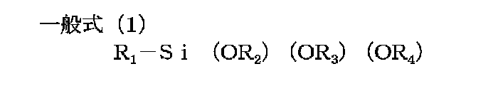
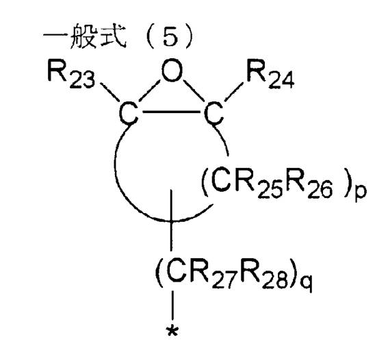
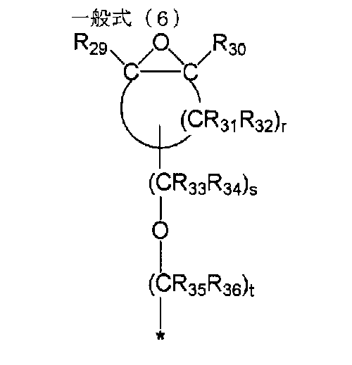
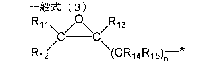
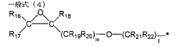
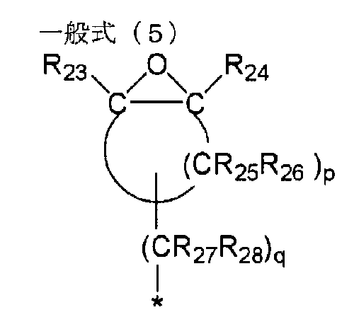
- R 1 represents a hydrocarbon group represented by any of the following general formulas (3) to (6)
- R 2 to R 4 each independently represents a hydrocarbon group.
- R 5 and R 6 each independently represent a linear or branched alkyl group having 1 to 20 carbon atoms
- R 7 to R 10 each independently represents a hydrogen atom, carbon
- An alkyl group having 1 to 3 carbon atoms or an alkoxy group having 1 to 3 carbon atoms is represented.
- R 11 to R 13 , R 16 to R 18 , R 23 , R 24 , R 29 , and R 30 are each independently a hydrogen atom or an alkyl group having 1 to 4 carbon atoms.
- R 14 , R 15 , R 19 to R 22 , R 27 , R 28 , and R 33 to R 36 each independently represent a hydrogen atom or an alkyl group having 1 to 4 carbon atoms.
- R 25 , R 26 , R 31 and R 32 each independently represent a hydrogen atom, an alkoxyl group having 1 to 4 carbon atoms or an alkyl group having 1 to 4 carbon atoms.
- n, m, l, q, s and t each independently represent an integer of 1 to 8.
- p and r each independently represents an integer of 4 to 12.
- “*” represents a bonding position with the silicon atom of the general formula (1).
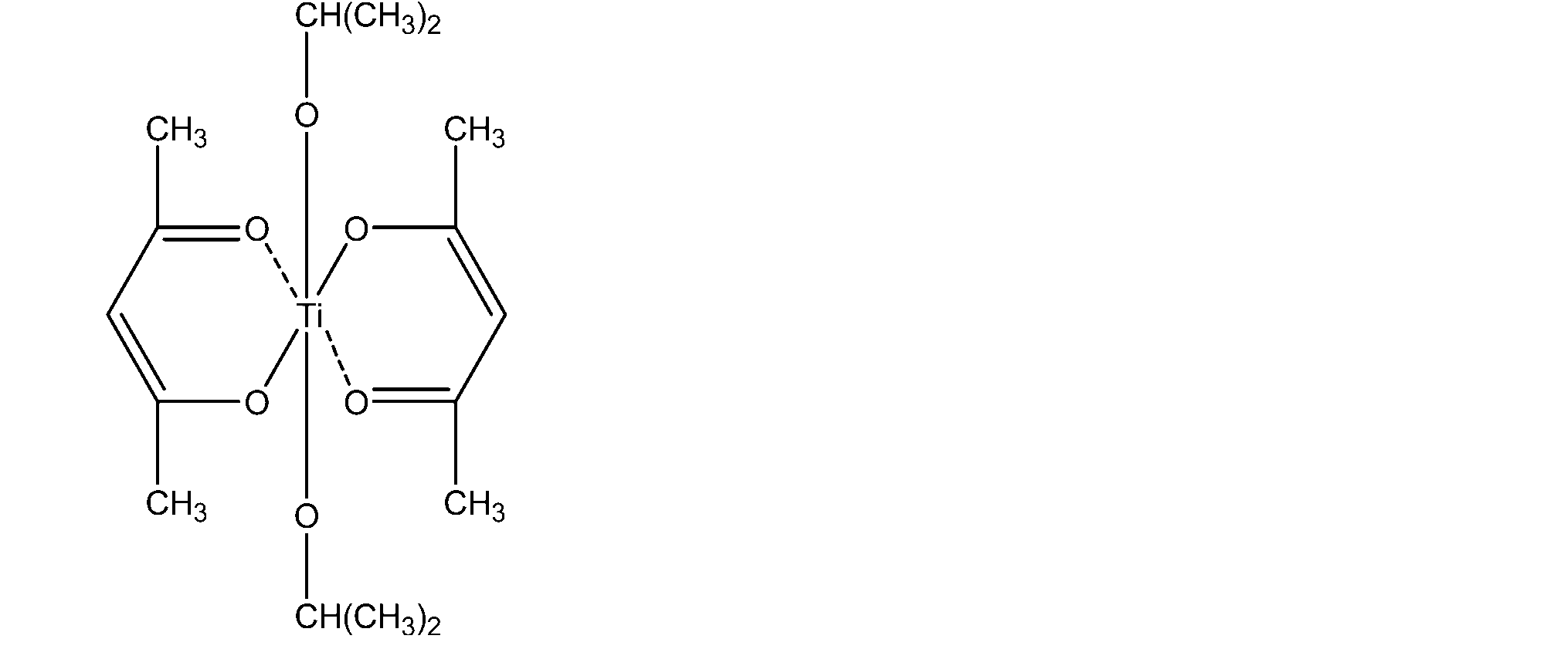
- the present invention also provides a polysiloxane comprising a hydrolytic condensate of a hydrolyzable silane compound represented by the general formula (1) and a chelate titanium compound represented by the general formula (2). It is the coating liquid for formation of the film
- a coating liquid used for forming a film containing polysiloxane in which white turbidity and precipitation are suppressed and occurrence of coating unevenness and the like are suppressed.
- an electrophotographic member comprising a thin film containing polysiloxane having a high dielectric constant as a surface layer, having excellent charging performance, and contributing to the formation of a high-quality electrophotographic image.
- FIG. 1 is a cross-sectional view of an electrophotographic apparatus according to the present invention.
- 1 is a schematic diagram of a surface potential measuring device for a photosensitive drum.
- FIG. 1 shows a cross section of an electrophotographic member according to an embodiment of the present invention.
- the electrophotographic member has a base 101, a conductive elastic layer 102, and a surface layer 103.
- a substrate having conductivity is used as the substrate. Specific examples include the following.
- a metal (alloy) substrate made of iron, copper, stainless steel, aluminum, aluminum alloy or nickel.
- the conductive elastic layer one type or two or more types of elastic bodies such as rubber used in conventional elastic layers (conductive elastic layers) such as charging members can be used.
- the rubber include the following. Urethane rubber, silicone rubber, butadiene rubber, isoprene rubber, chloroprene rubber, styrene-butadiene rubber, ethylene-propylene rubber, polynorbornene rubber, styrene-butadiene-styrene rubber, acrylonitrile rubber, epichlorohydrin rubber and alkyl ether rubber.
- the electroconductivity can be set to a predetermined value by appropriately using a conductive agent in the conductive elastic layer.
- the electrical resistance value of the conductive elastic layer can be adjusted by appropriately selecting the type and amount of the conductive agent, and the preferred range of the electrical resistance value is 10 2 to 10 8 ⁇ , which is more suitable. The range is 10 3 to 10 6 ⁇ .
- a conductive agent for the conductive elastic layer conductive carbon such as ketjen black EC, acetylene black, carbon for rubber, carbon for color (ink) subjected to oxidation treatment, and pyrolytic carbon should be used. You can also.
- graphite such as natural graphite and artificial graphite can also be used as a conductive agent for the conductive elastic layer.
- An inorganic or organic filler or a crosslinking agent may be added to the conductive elastic layer.
- the conductive elastic layer is formed on the substrate by mixing the raw materials of the conductive elastic layer with a hermetic mixer or the like and using a known method such as extrusion molding, injection molding, or compression molding.
- the conductive elastic layer is bonded onto the substrate via an adhesive as necessary.
- the conductive elastic layer formed on the substrate is vulcanized as necessary.
- volatile by-products such as a vulcanization accelerator due to the vulcanization reaction are gasified and cause voids. Therefore, it is preferable to perform vulcanization in the second zone after sufficiently removing the gas component by dividing the heating zone into two and maintaining the first zone lower than the vulcanization temperature.
- the coating solution for forming the surface layer is a hydrolysis condensate obtained by hydrolyzing and condensing a hydrolyzable silane compound represented by the following general formula (1) and a chelate titanium compound represented by the following general formula (2). including.
- a surface comprising a polysiloxane thin film by coating the coating liquid on the surface of the elastic layer and then cleaving the epoxy group in the hydrolysis condensate in the coating to crosslink the hydrolysis condensate. Form a layer.
- R 1 represents a hydrocarbon group having an epoxy group represented by any of the following general formulas (3) to (6).
- R 2 to R 4 each independently represents a hydrocarbon group. Specific examples of the hydrocarbon group according to R 2 to R 4 include an alkyl group having 1 to 4 carbon atoms.
- R 5 and R 6 each independently represents a linear or branched alkyl group having 1 to 20 carbon atoms, preferably a lower alkyl having 1 to 3 carbon atoms. It is a group.
- R 7 to R 10 each independently represent a hydrogen atom, an alkyl group having 1 to 3 carbon atoms, or an alkoxy group having 1 to 3 carbon atoms.
- R 11 to R 13 , R 16 to R 18 , R 23 , R 24 , R 29 , and R 30 are each independently a hydrogen atom or an alkyl having 1 to 4 carbon atoms.
- R 14 , R 15 , R 19 to R 22 , R 27 , R 28 and R 33 to R 36 each independently represent a hydrogen atom or an alkyl group having 1 to 4 carbon atoms.
- R 25 , R 26 , R 31 and R 32 each independently represent a hydrogen atom, an alkoxyl group having 1 to 4 carbon atoms or an alkyl group having 1 to 4 carbon atoms.
- n, m, l, q, s, and t each independently represent an integer of 1 or more and 8 or less.
- p and r each independently represent an integer of 4 or more and 12 or less.
- “*” represents a bonding position with the silicon atom of the general formula (1).
- hydrolyzable silane compound having the structure represented by the general formula (3) are shown below.
- hydrolyzable silane compound having the structure represented by the general formula (4) are shown below.
- hydrolyzable silane compound having the structure represented by the general formula (5) are shown below.
- (5-1) 2- (3,4-epoxycyclohexyl) ethyltrimethoxysilane
- (5-2) 2- (3,4-epoxycyclohexyl) ethyltriethoxysilane.
- hydrolyzable silane compound having the structure represented by the general formula (6) are shown below.
- the hydrolyzable silane compound represented by the general formula (1) has a very fast dehydration / condensation reaction. Therefore, the coating solution for forming the surface layer needs to be further improved due to storage stability. That is, dehydration condensation of the silane compound represented by the general formula (1) proceeds in the coating liquid, and polysiloxane is generated in the coating liquid and may become cloudy.
- the chelate titanium compound represented by the general formula (2) has a slower reaction rate of hydrolysis compared to alkoxysilane. In other words, the stability to water is higher than that of alkoxysilane. Therefore, the storage stability as the coating liquid can be improved by allowing the alkoxysilane represented by the above formula (1) and the chelate titanium compound represented by the above formula (2) to coexist in the coating liquid. it is conceivable that.
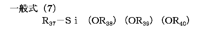
- hydrolysis condensate in addition to the hydrolyzable silane compound represented by the general formula (1) and the chelate titanium compound represented by the general formula (2), the hydrolysis represented by the following general formula (7) A decomposable silane compound may be used.
- R 37 represents an aryl group such as an alkyl group having 1 to 10 carbon atoms or a phenyl group.
- R 38 to R 40 each independently represent a hydrocarbon group, specifically, for example, an alkyl group having 1 to 4 carbon atoms.
- hydrolyzable silane compound having the structure represented by the general formula (7) are shown below.
- R 37 is a hydrolyzable silane compound having a linear alkyl group having 6 to 10 carbon atoms, and R 37 is a phenyl group. It is preferable to combine a hydrolyzable silane compound having In this case, the compatibility with the solvent is good even if the monomer structure is changed by the hydrolysis / condensation reaction.
- R 41 to R 44 each independently represent a hydrocarbon group.
- specific examples of the hydrocarbon group include an alkyl group having 1 to 6 carbon atoms.
- the general formula (7) it is also possible to use a hydrolyzable silane compound having a structure represented by the formula (8) and a hydrolyzable titanium compound represented by the general formula (8).
- hydrolyzable titanium compound having the structure represented by the general formula (8) are shown below.
- a cationic polymerization catalyst as a photopolymerization initiator is allowed to coexist from the viewpoint of improving the crosslinking efficiency.
- an epoxy group exhibits high reactivity with respect to an onium salt of a Lewis acid activated by an active energy ray
- the above cationic polymerizable group is an epoxy group. It is preferable to use an onium salt of an acid.
- Examples of other cationic polymerization catalysts include borate salts, compounds having an imide structure, compounds having a triazine structure, azo compounds, and peroxides.
- aromatic sulfonium salts and aromatic iodonium salts are preferable from the viewpoints of sensitivity, stability, and reactivity.
- a compound having the structure shown (trade name: Irgacure 261, manufactured by Ciba Specialty Chemicals) is preferred.
- Production Example 1 is a production method using a compound having a structure represented by General Formula (1) and General Formula (2).
- Production Example 2 is a production method using a compound having a structure represented by General Formula (1), General Formula (2), General Formula (7) and General Formula (8).
- the manufacturing method example 1 includes the following first step (i) and second step (ii).
- a coating film of a coating liquid containing a hydrolysis condensate of a compound having a structure represented by the general formula (1) and a compound having a structure represented by the general formula (2) is disposed on the outer periphery of the substrate.
- step (i) of Production Method Example 2 a chelating titanium compound, a hydrolysable titanium compound, water and an alcohol are added to the hydrolyzable silane compound, and hydrolysis and condensation are performed by heating under reflux (iii) (first) Step reaction) is carried out.
- the hydrolyzable compound represented by the general formula (8) is added to the solution obtained in the step (iii) without adding the hydrolyzable titanium compound represented by the general formula (8).
- a step (iv) (second stage reaction) in which a titanium compound is added to perform hydrolysis / condensation may be provided separately.
- step (ii) through step (v) of adding the photopolymerization initiator to the solution obtained in step (iv).
- the two-step synthesis reaction of steps (iii) and (iv) is because the reaction rate of the hydrolyzable silane compound and the reaction rate of the hydrolyzable titanium compound are very different, that is, in the general formula (8) This is because the reaction rate of the hydrolyzable titanium compound shown is very fast.
- the chelated titanium compound represented by the general formula (2) which prevents precipitation and cloudiness when the amount of water added in step (i) and the amount of water in the alcohol are excessive, It is more effective to divide into two stages.
- the liquid When the chelated titanium compound is not added, or when the amount of water is large and the amount of the hydrolyzable titanium compound is large, the liquid may become cloudy or precipitate. This precipitation is the generation of TiO 2 fine particles. In order to perform coating without uneven coating, generation of fine particles is not preferable.
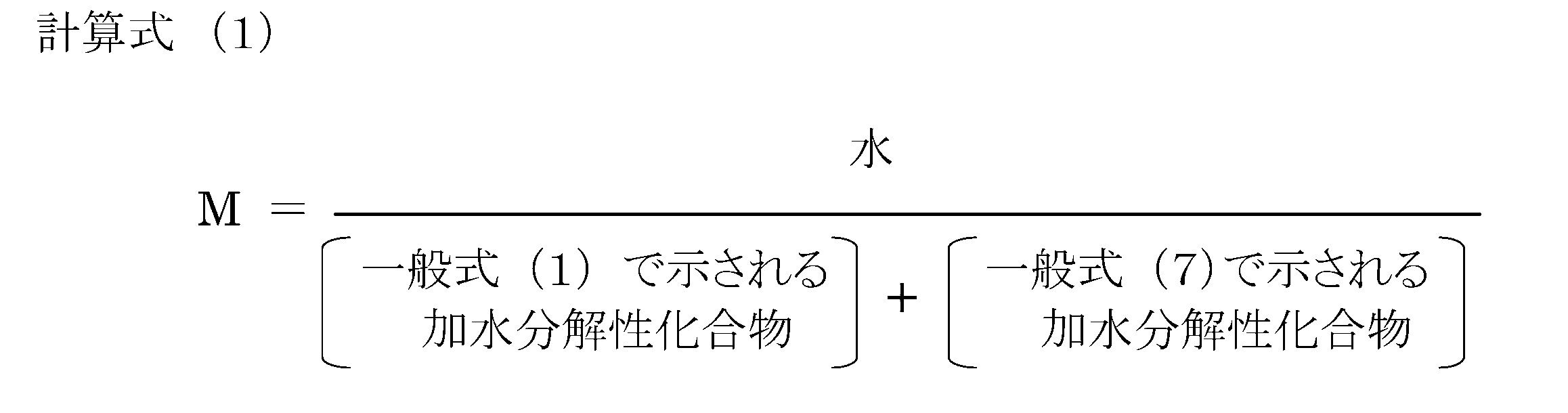
- the ratio M (molar ratio) of the amount of water added to the hydrolyzable silane compound when synthesizing the coating liquid is preferably 0.3 or more and 9.0 or less.
- This value is more preferably 1.2 or more and 3.0 or less. If the amount of water added is within the above range, the degree of condensation during synthesis can be easily controlled. Further, the condensation rate can be easily controlled, and the life of the coating solution is also effective.
- a primary alcohol a mixed system of a primary alcohol and a secondary alcohol, or a mixed system of a primary alcohol and a tertiary alcohol as the alcohol for synthesizing the coating liquid.
- ethanol alone, a mixed system of methanol / 2-butanol, or a mixed system of ethanol / 2-butanol is preferable.
- the obtained coating liquid is adjusted to an appropriate concentration and applied onto a substrate and a member having a conductive elastic layer formed on the substrate.
- an appropriate solvent considering volatility may be used in addition to the solvent used for the synthesis in order to improve the coating property.
- Suitable solvents include 2-butanol, ethyl acetate, methyl ethyl ketone, or a mixed system thereof.
- coating liquid when the coating liquid is applied on the conductive elastic layer, application using a roll coater, dip application, ring application, etc. can be employed.
- active energy rays are irradiated to the coating liquid applied on the conductive elastic layer. Then, the cationically polymerizable group contained in the coating solution is cleaved, whereby the coating solution can be cross-linked and cured by cross-linking.
- the active energy ray ultraviolet rays are preferable. If the cross-linking reaction is performed by ultraviolet rays, it is possible to suppress deterioration of the conductive elastic layer due to thermal history, and it is also possible to suppress a decrease in electrical characteristics of the conductive elastic layer.
- a high-pressure mercury lamp, a metal halide lamp, a low-pressure mercury lamp, an excimer UV lamp, or the like can be used.
- an ultraviolet ray source containing abundant light having an ultraviolet wavelength of 150 to 480 nm is used.
- the integrated light quantity of an ultraviolet-ray is defined like the following formula (2).
- the adjustment of the accumulated amount of ultraviolet light can be performed by the irradiation time, lamp output, and distance between the lamp and the irradiated object. Moreover, you may give a gradient to integrated light quantity within irradiation time.
- the integrated light amount of ultraviolet rays can be measured using an ultraviolet integrated light amount meter UIT-150-A or UVD-S254 manufactured by USHIO INC.
- the integrated light amount of ultraviolet rays can be measured using an ultraviolet integrated light amount meter UIT-150-A or VUV-S172 manufactured by USHIO INC.
- the electrophotographic member of the present invention can be used as a charging member, a developing roller, a transfer roller, a fixing unit, a cleaning blade, or the like in an electrophotographic apparatus.
- FIG. 2 shows an example of a schematic configuration of an electrophotographic apparatus provided with a process cartridge having the electrophotographic member (charging member) of the present invention.
- This electrophotographic apparatus has a cylindrical photoreceptor 1 that is driven to rotate at a predetermined peripheral speed in the direction of an arrow about an axis 2.
- the photoreceptor may have a support, a photosensitive layer formed on the support, a charge injection layer, a surface layer, and the like.
- the surface of the rotationally driven photoconductor is uniformly charged to a predetermined positive or negative potential by the charging member 3, and then exposure light (not shown) output from exposure means (not shown) for slit exposure or laser beam scanning exposure.
- exposure light (not shown) output from exposure means (not shown) for slit exposure or laser beam scanning exposure.
- image exposure light 4 an electrostatic latent image corresponding to the target image is formed.
- the electrostatic latent image formed on the surface of the photoreceptor 1 is supplied with a developer by a developing roller provided in the developing unit 5 and is reversely developed or normally developed to become a toner image.
- the toner image on the surface of the photoconductor 1 is transferred onto the transfer material such as paper that is conveyed between the photoconductor 1 and the transfer roller 6 in synchronization with the rotation of the photoconductor by a transfer bias applied to the transfer roller 6. Sequentially transferred to P.
- the transfer material P onto which the toner image has been transferred is separated from the surface of the photoreceptor 1 and is introduced into the fixing unit 8, and is printed out as an image formed product (print, copy) on which the toner image is fixed. .
- the image formed product is introduced into the recirculation transport mechanism and reintroduced into the transfer unit.
- the surface of the photoreceptor 1 after the transfer of the toner image is cleaned by removing the developer (toner) remaining after the transfer by a cleaning means 7 such as a cleaning blade, and further subjected to a charge removal process by pre-exposure light from the pre-exposure means. After that, it is repeatedly used for image formation.
- a cleaning means 7 such as a cleaning blade
- a process cartridge 9 in which the photosensitive member 1, the charging member 3, the developing means 5, and the cleaning means 7 are integrated is attached to and detached from the main body of the electrophotographic apparatus via a guide means 10 such as a rail of the main body of the electrophotographic apparatus. It is attached as possible.
- the cartridge can be appropriately selected from transfer means or the like, and can be attached to and detached from the electrophotographic apparatus body.
- part means “part by mass”.
- thermosetting adhesive containing metal and rubber (trade name: METALOC N-33, manufactured by Toyo Chemical Laboratory Co., Ltd.) was applied and dried at a temperature of 80 ° C. for 30 minutes. It was dried at a temperature of 120 ° C. for 1 hour.
- the kneaded product I was extruded coaxially onto the peripheral surface of the substrate on which the adhesive layer had been formed so as to have a cylindrical shape with an outer diameter of 8.75 to 8.90 mm. Then, the edge part of the cylindrical kneaded material I was cut
- the layer of the unvulcanized kneaded material I covering the outer periphery of the substrate was vulcanized using a continuous heating furnace having two zones set at different temperatures. Specifically, in the first zone, the temperature was set to 80 ° C., and the substrate was passed through in 30 minutes. Thereafter, the conductive elastic layer is formed by passing the second zone set at 160 ° C. over 30 minutes to vulcanize the layer of the unvulcanized kneaded product I and coat the outer peripheral portion of the substrate. Formed.
- both ends of the conductive elastic layer were cut so that the width of the conductive elastic layer portion in the axial direction was 232 mm.
- the surface of the conductive elastic layer was polished with a rotating grindstone to obtain a conductive elastic roller-1 having a crown-shaped conductive elastic layer having an end diameter of 8.26 mm and a central diameter of 8.5 mm.
- the mixture of the above components was stirred at room temperature (23 ° C.) for 30 minutes, and then stirred while heating using an oil bath.
- the oil is heated so that the temperature reaches 120 ° C. 20 minutes after the start of heating, and then the oil temperature is maintained at 120 ° C. and heated under reflux for 5 hours to obtain a condensate intermediate-1. It was. Note that the number of rotations was 300 rpm for both stirring at room temperature and under heating.
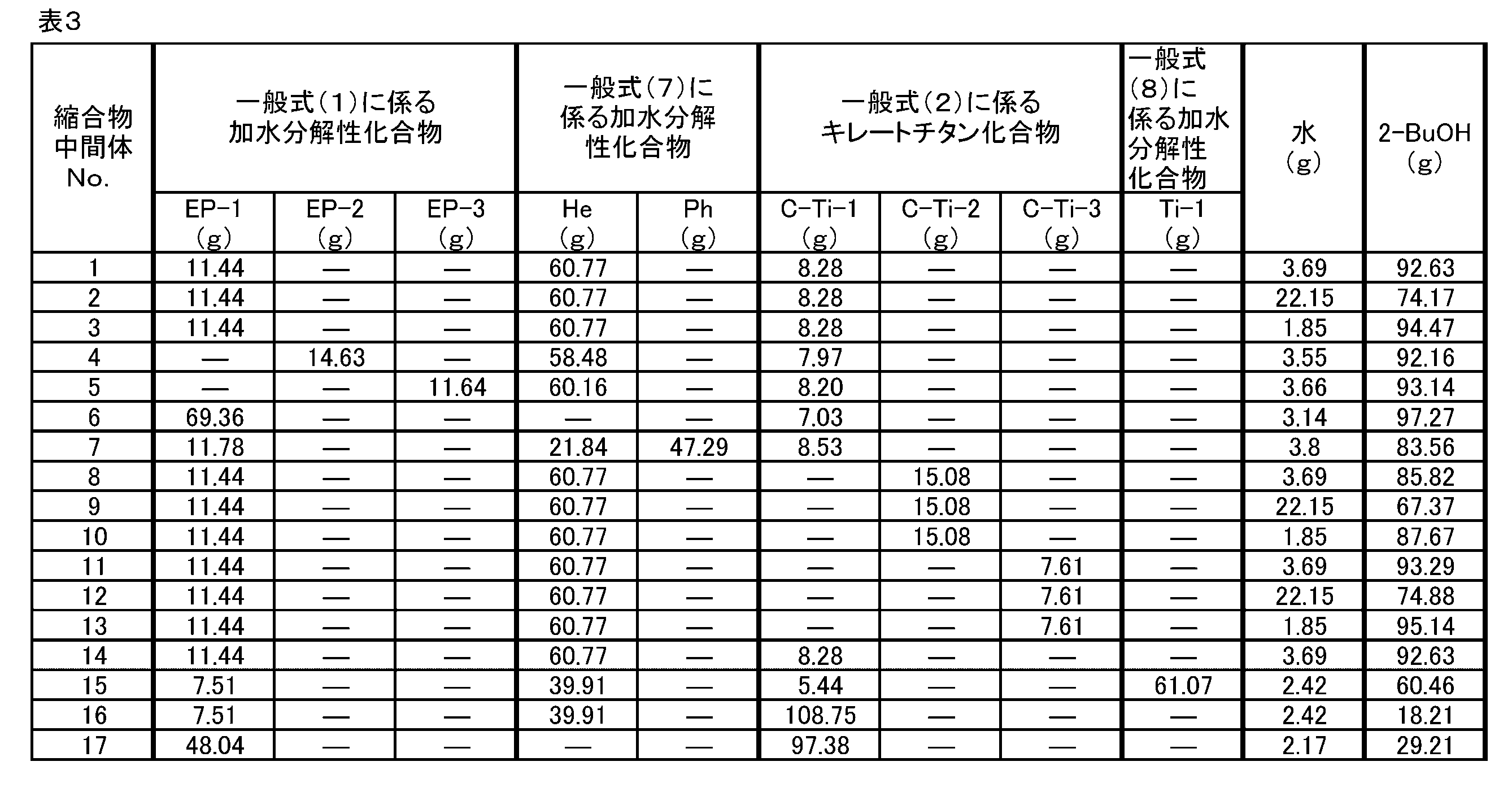
- Condensate intermediates 2 to 17 were prepared in the same manner as the condensate intermediate-1 except that the formulation shown in Table 3 was used.
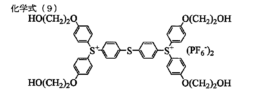
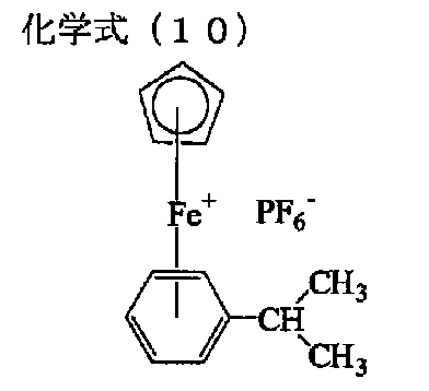
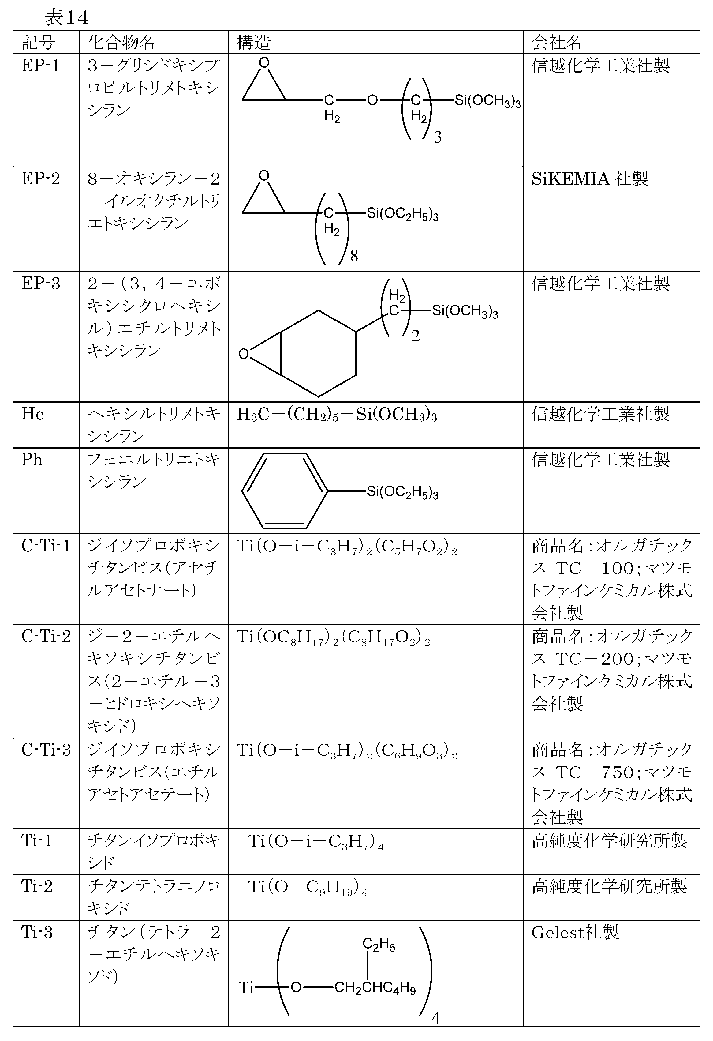
- Table 3 the symbols “EP-1” to “EP-3”, “He”, “Ph”, “C-Ti-1” to “C-Ti-3”, and “Ti-1”
- the compounds shown in Table 14 are represented.
- Condensates 1-2 to 1-3 were prepared in the same manner as condensate 1-1 except that the blending amount of condensate intermediate-1 and the blending amount of Ti-1 were changed as shown in Table 4. .
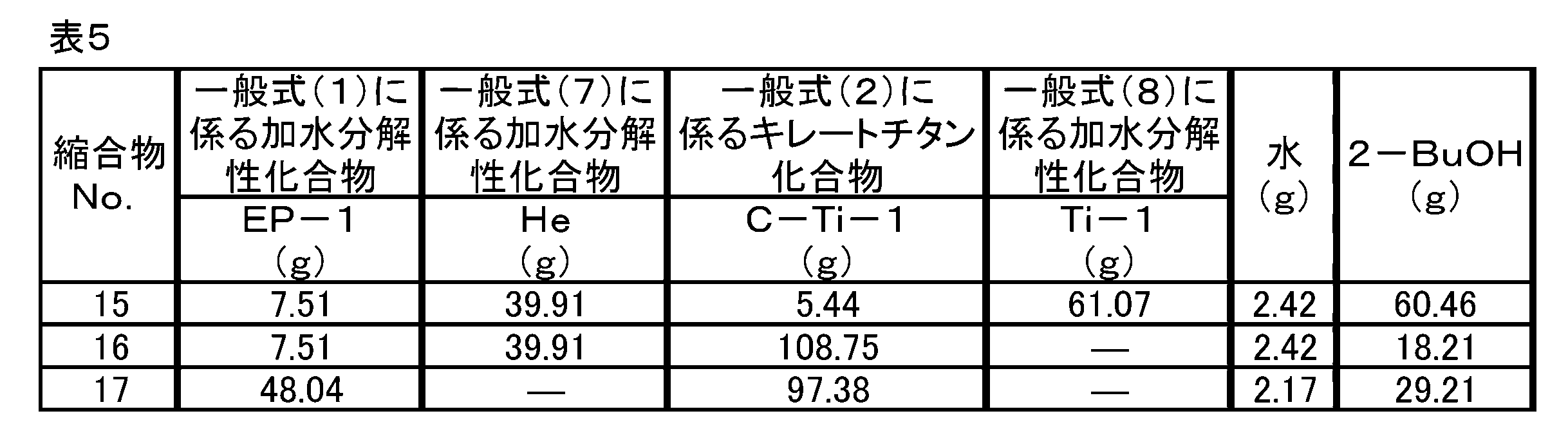
- Condensates 15 to 17 were prepared in the same manner as the condensate 1-1 except that the formulation shown in Table 5 below was used.
- the symbols “EP-1”, “He”, “C—Ti-1” and “Ti-1” in Table 5 each represent a compound shown in Table 14.
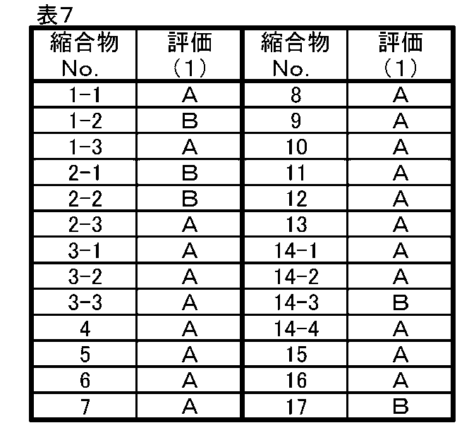
- Table 7 shows the result of evaluation (1).
- the coating liquid 1-1 to 1-3, 2 to 1 to 2-3, 3-1 to 3-3, 4 to 13, 14-1 to 14-4, 15 ⁇ 17 were prepared.
- a polymerization initiator solution was prepared so that an aromatic sulfonium salt [trade name: Adekaoptomer SP-150, manufactured by Adeka Co., Ltd.] as a photocationic polymerization initiator was 10% by mass in methanol. . Subsequently, this polymerization initiator solution was added at a ratio of 331.43 g with respect to 1 mol of R 1 group in each condensate. Thereafter, the theoretical solid content is adjusted with ethanol so as to have the concentration shown in Table 13, and the coating liquids 1-1 to 1-3, 2 to 1-2, 3-1 to 3-3, 4 to 13 are prepared. 14-1 to 14-4 and 15 to 17 were prepared.
- each coating liquid prepared above was applied onto the conductive elastic roller 1 in a ring (discharge amount: 0.120 ml / s (ring part speed: 85 mm / s, total discharge amount: 0.130 ml).
- Table 13 shows the evaluation results. Further, when the electrophotographic member according to each example was used as a charging roller and image evaluation was performed, an image to be specially noted is equivalent to a member produced without using the chelate titanium compound of the general formula (2). Confirmed that there were no harmful effects.
- Patent Document 1 shows that the smaller this value, the better the positive ghost level at both low speed and high speed.
- a coating liquid C-1 was prepared in the same manner as the coating liquid 1-1 except that the condensate C-1 was used and no photocationic polymerization initiator was used.
- Electrophotographic Member C-1 An electrophotographic member C-1 was produced in the same manner as the electrophotographic member 1-1 except that this coating solution was used, and was subjected to evaluations (2) to (3).
- Table 13 shows the results of evaluations (2) to (3) for the electrophotographic members according to Examples 1 to 17 and Comparative Examples 1 and 2.
Abstract
Description


R14、R15、R19~R22、R27、R28、及びR33~R36は各々独立に水素原子、又は炭素数1~4のアルキル基を示す。
R25、R26、R31及びR32は各々独立に水素原子、炭素数1~4のアルコキシル基又は炭素数1~4のアルキル基を示す。
n、m、l、q、s及びtは、各々独立に1~8の整数を示す。p及びrは各々独立に4~12の整数を示す。また、「*」は、一般式(1)のケイ素原子との結合位置を示す。 In the general formulas (3) to (6), R 11 to R 13 , R 16 to R 18 , R 23 , R 24 , R 29 , and R 30 are each independently a hydrogen atom or an alkyl group having 1 to 4 carbon atoms. , A hydroxyl group, a carboxyl group, or an amino group.
R 14 , R 15 , R 19 to R 22 , R 27 , R 28 , and R 33 to R 36 each independently represent a hydrogen atom or an alkyl group having 1 to 4 carbon atoms.
R 25 , R 26 , R 31 and R 32 each independently represent a hydrogen atom, an alkoxyl group having 1 to 4 carbon atoms or an alkyl group having 1 to 4 carbon atoms.
n, m, l, q, s and t each independently represent an integer of 1 to 8. p and r each independently represents an integer of 4 to 12. Further, “*” represents a bonding position with the silicon atom of the general formula (1).
基体としては導電性を有するものを用いる。具体例としては、以下のものが挙げられる。鉄、銅、ステンレス鋼、アルミニウム、アルミニウム合金又はニッケルで形成されている金属製(合金製)の基体。 [Substrate]
A substrate having conductivity is used as the substrate. Specific examples include the following. A metal (alloy) substrate made of iron, copper, stainless steel, aluminum, aluminum alloy or nickel.
導電性弾性層には、従来の帯電部材などの弾性層(導電性弾性層)に用いられているゴムなどの弾性体を1種又は2種以上用いることができる。ゴムとしては以下のものが挙げられる。ウレタンゴム、シリコーンゴム、ブタジエンゴム、イソプレンゴム、クロロプレンゴム、スチレン-ブタジエンゴム、エチレン-プロピレンゴム、ポリノルボルネンゴム、スチレン-ブタジエン-スチレンゴム、アクリロニトリルゴム、エピクロルヒドリンゴム及びアルキルエーテルゴム。 [Elastic layer]
As the conductive elastic layer, one type or two or more types of elastic bodies such as rubber used in conventional elastic layers (conductive elastic layers) such as charging members can be used. Examples of the rubber include the following. Urethane rubber, silicone rubber, butadiene rubber, isoprene rubber, chloroprene rubber, styrene-butadiene rubber, ethylene-propylene rubber, polynorbornene rubber, styrene-butadiene-styrene rubber, acrylonitrile rubber, epichlorohydrin rubber and alkyl ether rubber.
〔表面層用コーティング液〕
表面層形成用コーティング液は下記一般式(1)で示される加水分解性シラン化合物と、下記一般式(2)で示されるキレートチタン化合物とを加水分解・縮合させることにより得られる加水分解縮合物を含む。該コーティング液を弾性層の表面に塗膜した後、該塗膜中の、該加水分解縮合物中のエポキシ基を開裂させることにより、該加水分解縮合物を架橋させてポリシロキサン薄膜からなる表面層を形成する。 [Surface layer]
[Coating liquid for surface layer]
The coating solution for forming the surface layer is a hydrolysis condensate obtained by hydrolyzing and condensing a hydrolyzable silane compound represented by the following general formula (1) and a chelate titanium compound represented by the following general formula (2). including. A surface comprising a polysiloxane thin film by coating the coating liquid on the surface of the elastic layer and then cleaving the epoxy group in the hydrolysis condensate in the coating to crosslink the hydrolysis condensate. Form a layer.

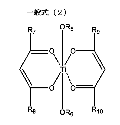
また、一般式(2)中、R5及びR6は各々独立に、炭素原子数1~20の直鎖状または分岐鎖状のアルキル基を示し、好ましくは、炭素数1~3の低級アルキル基である。さらに、R7~R10は各々独立に水素原子、炭素数1~3のアルキル基または炭素数1~3のアルコキシ基を示す。 In the general formula (1), R 1 represents a hydrocarbon group having an epoxy group represented by any of the following general formulas (3) to (6). R 2 to R 4 each independently represents a hydrocarbon group. Specific examples of the hydrocarbon group according to R 2 to R 4 include an alkyl group having 1 to 4 carbon atoms.
In the general formula (2), R 5 and R 6 each independently represents a linear or branched alkyl group having 1 to 20 carbon atoms, preferably a lower alkyl having 1 to 3 carbon atoms. It is a group. R 7 to R 10 each independently represent a hydrogen atom, an alkyl group having 1 to 3 carbon atoms, or an alkoxy group having 1 to 3 carbon atoms.

n、m、l、q、s及びtは、各々独立に1以上8以下の整数を示す。p及びrは、各々独立に4以上12以下の整数を示す。また、「*」は、一般式(1)のケイ素原子との結合位置を示す。 In the general formulas (3) to (6), R 11 to R 13 , R 16 to R 18 , R 23 , R 24 , R 29 , and R 30 are each independently a hydrogen atom or an alkyl having 1 to 4 carbon atoms. A group, a hydroxyl group, a carboxyl group or an amino group; R 14 , R 15 , R 19 to R 22 , R 27 , R 28 and R 33 to R 36 each independently represent a hydrogen atom or an alkyl group having 1 to 4 carbon atoms. R 25 , R 26 , R 31 and R 32 each independently represent a hydrogen atom, an alkoxyl group having 1 to 4 carbon atoms or an alkyl group having 1 to 4 carbon atoms.
n, m, l, q, s, and t each independently represent an integer of 1 or more and 8 or less. p and r each independently represent an integer of 4 or more and 12 or less. Further, “*” represents a bonding position with the silicon atom of the general formula (1).


以下に、本発明の電子写真用部材の製造方法を例示する。製法例1は、一般式(1)及び一般式(2)で示される構造を有する化合物を用いて製造する方法である。また製法例2は、一般式(1)、一般式(2)、一般式(7)及び一般式(8)で示される構造を有する化合物を用いて製造する方法である。 [Method for producing electrophotographic member]
Below, the manufacturing method of the member for electrophotography of this invention is illustrated. Production Example 1 is a production method using a compound having a structure represented by General Formula (1) and General Formula (2). In addition, Production Example 2 is a production method using a compound having a structure represented by General Formula (1), General Formula (2), General Formula (7) and General Formula (8).
(i)一般式(1)で示される構造を有する化合物と、一般式(2)で示される構造を有する化合物との加水分解縮合物を含むコーティング液の塗膜を、基体の外周に配置された弾性層の上に形成する第1の工程。
(ii)該加水分解縮合物のR1のエポキシ基を開裂させることにより該加水分解縮合物を架橋させて表面層を形成する第2の工程。 The manufacturing method example 1 includes the following first step (i) and second step (ii).
(I) A coating film of a coating liquid containing a hydrolysis condensate of a compound having a structure represented by the general formula (1) and a compound having a structure represented by the general formula (2) is disposed on the outer periphery of the substrate. A first step of forming on the elastic layer.
(Ii) A second step of forming a surface layer by crosslinking the hydrolysis condensate by cleaving the R 1 epoxy group of the hydrolysis condensate.

本発明の電子写真用部材は、電子写真装置における、帯電部材、現像ローラ、転写ローラ、定着手段、クリーニングブレード等として用いることができる。 [Electrophotographic equipment]
The electrophotographic member of the present invention can be used as a charging member, a developing roller, a transfer roller, a fixing unit, a cleaning blade, or the like in an electrophotographic apparatus.
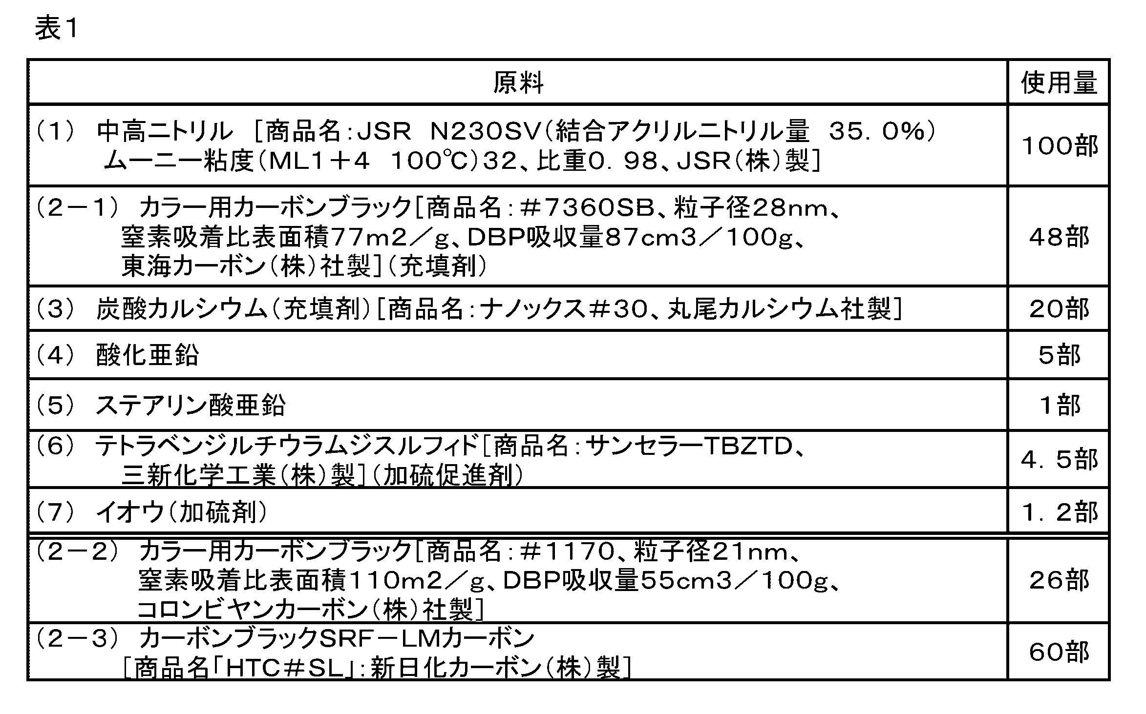
〔1〕導電性弾性ローラの作製及び評価
〔導電性弾性ローラ1の作製〕
表1に示す量の成分(1)、(2-1)、(3)、(4)及び(5)、を6Lニーダーで20分間混練し、次いで表1に示す量の成分(6)及び(7)を加え、オープンロールでさらに8分間混練することによって、混練物Iを得た。 [Examples 1 to 14, Reference Examples 1 and 2]
[1] Production and evaluation of conductive elastic roller [Production of conductive elastic roller 1]
The components (1), (2-1), (3), (4) and (5) in the amounts shown in Table 1 were kneaded for 20 minutes in a 6 L kneader, and then the components (6) and in the amounts shown in Table 1 were used. (7) was added and kneaded product I was obtained by kneading for 8 minutes with an open roll.
<縮合物中間体-1の合成>
下記表2の材料を300mlのナスフラスコに入れ、混合した。 [2] Preparation and Evaluation of Coating Solution for Surface Layer Formation <Synthesis of Condensate Intermediate-1>
The materials shown in Table 2 below were placed in a 300 ml eggplant flask and mixed.
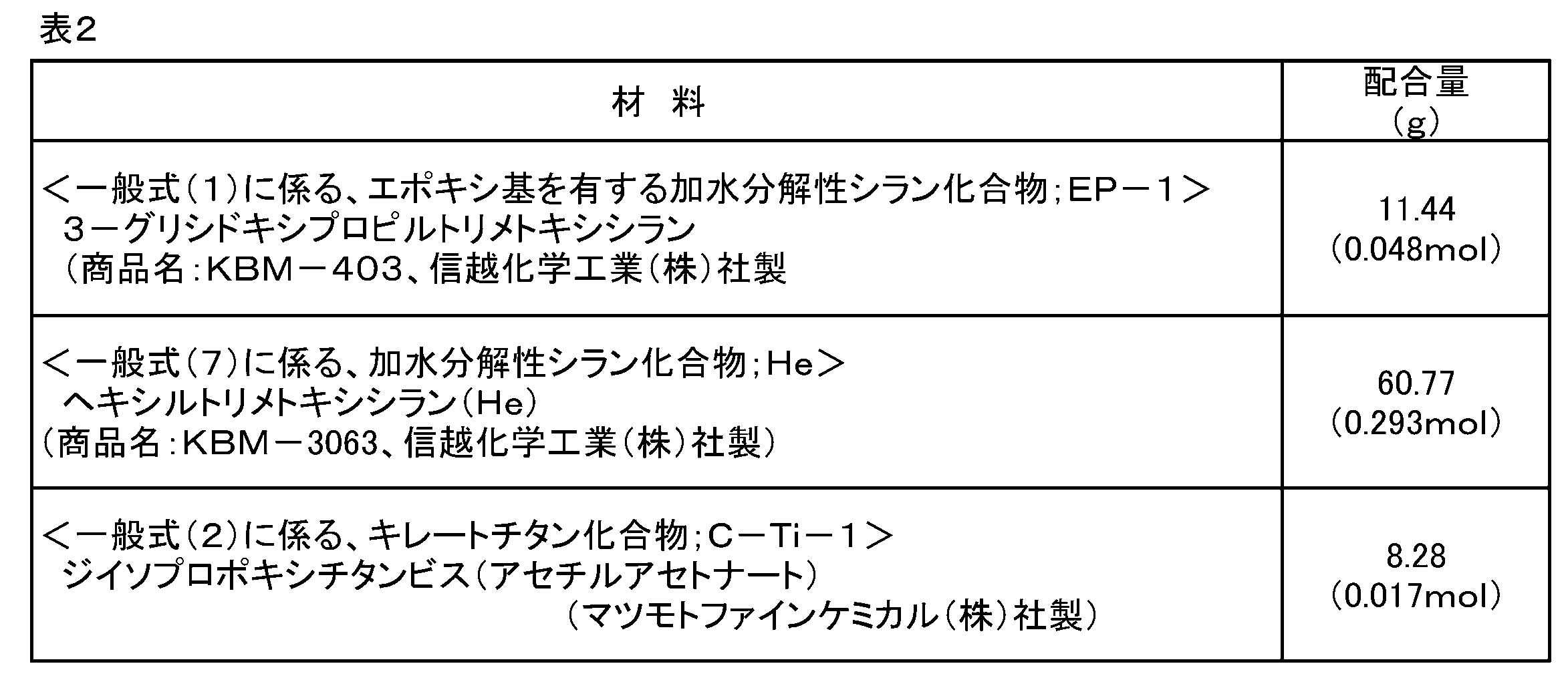
下記表3に記載の配合としたこと以外は、縮合物中間体-1と同様にして縮合物中間体-2~17を調製した。なお、表3における記号「EP-1」~「EP-3」、「He」、「Ph」、「C-Ti-1」~「C-Ti-3」、「Ti-1」は、各々表14に示す化合物を表す。
<Preparation of
縮合物中間体-1の116.28gを、300mlのナスフラスコに入れた。そこに、テトライソプロポキシチタン(Ti-1)[(株)高純度化学研究所製]60.52g(0.211mol)を添加し、室温で3時間攪拌して、加水分解及び縮合反応を行って縮合物1-1を得た。攪拌時の回転数は300rpmとした。 <Synthesis of Condensate 1-1>
116.28 g of condensate intermediate-1 was placed in a 300 ml eggplant flask. Thereto was added 60.52 g (0.211 mol) of tetraisopropoxy titanium (Ti-1) [manufactured by Kojundo Chemical Laboratory Co., Ltd.] and stirred at room temperature for 3 hours to conduct hydrolysis and condensation reactions. Thus, a condensate 1-1 was obtained. The number of rotations during stirring was 300 rpm.
縮合物中間体-1の配合量及びTi-1の配合量を表4に示したように変更したこと以外は縮合物1-1と同様にして縮合物1-2~1-3を調製した。 <Preparation of condensates 1-2 to 1-3>
Condensates 1-2 to 1-3 were prepared in the same manner as condensate 1-1 except that the blending amount of condensate intermediate-1 and the blending amount of Ti-1 were changed as shown in Table 4. .
縮合物中間体及びその配合量、ならびにTi-1~Ti-3の配合量を表4に示したように変更したこと以外は縮合物1-1と同様にして縮合物2~1~2-3、3-1~3-3、4~13、14-1~14-4を調製した。なお、表4における記号「Ti-1」~「Ti-3」は、各々表14に示す化合物を表す。 <Preparation of

下記表5に記載の配合としたこと以外は、縮合物1-1と同様にして縮合物15~17を調製した。なお、表5における記号「EP-1」、「He」、「C-Ti-1」及び「Ti-1」は、各々表14に示す化合物を表す。 <Preparation of condensates 15-17>
Condensates 15 to 17 were prepared in the same manner as the condensate 1-1 except that the formulation shown in Table 5 below was used. The symbols “EP-1”, “He”, “C—Ti-1” and “Ti-1” in Table 5 each represent a compound shown in Table 14.
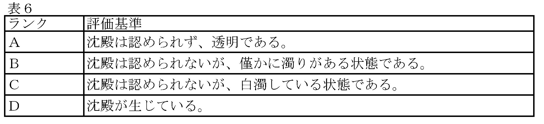
縮合物の外観を目視で観察し、下記表6に記載の基準に従って評価した。 [Evaluation (1): Condensate stability]
The appearance of the condensate was visually observed and evaluated according to the criteria described in Table 6 below.
各縮合物を用いて以下の手順で、コーティング液1-1~1-3、2~1~2-3、3-1~3-3、4~13、14-1~14-4、15~17を調製した。 <Preparation of coating solution>
Using each condensate, the coating liquid 1-1 to 1-3, 2 to 1 to 2-3, 3-1 to 3-3, 4 to 13, 14-1 to 14-4, 15 ~ 17 were prepared.
<コーティング液の塗膜の形成>
次に、導電性弾性ローラ1上に上記で調製した各コーティング液をリング塗布(吐出量:0.120ml/s(リング部のスピード:85mm/s、総吐出量:0.130ml)した。 [3] Production and evaluation of electrophotographic member <Formation of coating film of coating solution>
Next, each coating liquid prepared above was applied onto the conductive
次いでリング塗布された各コーティング液の塗膜に対して、254nmの波長の紫外線を積算光量が9000mJ/cm2になるように照射した。なお、紫外線の照射には、低圧水銀ランプ(ハリソン東芝ライティング(株)製)を用いた。これにより、塗膜を架橋、硬化させて、厚さが100nmの表面層を形成し、電子写真用部材1-1~1-3、2~1~2-3、3-1~3-3、4~13、14-1~14-4、15~17を作製した。得られた電子写真用部材を下記の評価(2)~(3)に供した。 <Curing of coating film of coating liquid, formation of surface layer>
Next, ultraviolet rays having a wavelength of 254 nm were applied to the coating film of each coating liquid applied with a ring so that the integrated light amount was 9000 mJ / cm 2 . A low-pressure mercury lamp (manufactured by Harrison Toshiba Lighting Co., Ltd.) was used for ultraviolet irradiation. As a result, the coating film is crosslinked and cured to form a surface layer having a thickness of 100 nm, and the electrophotographic members 1-1 to 1-3, 2 to 1 to 2-3, and 3-1 to 3-3. 4 to 13, 14-1 to 14-4, and 15 to 17 were produced. The obtained electrophotographic member was subjected to the following evaluations (2) to (3).
得られた電子写真用部材の表面層の外観を目視で観察し、コーティング液の塗膜形成時の塗工性を下記表8に示した基準に従って評価した。 [Evaluation (2): Evaluation of coating properties of coating solution]
The appearance of the surface layer of the obtained electrophotographic member was visually observed, and the coating properties when the coating solution was formed were evaluated according to the criteria shown in Table 8 below.

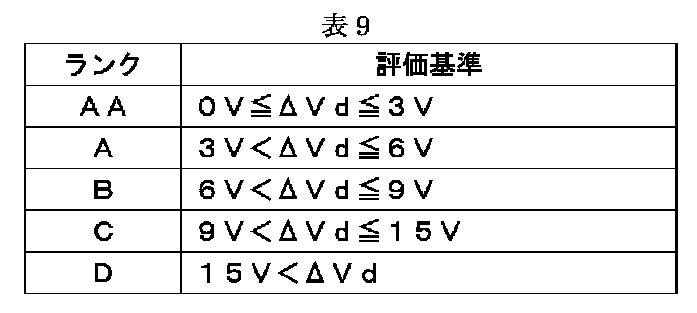
プロセススピードに対する帯電能力の評価として、図3に示す装置を用いた。感光体ドラム表面電位は、感光体ドラム21に接触した帯電部材22に帯電バイアス電源S1から所定の帯電バイアスを印加し、露光装置23から感光体ドラムを画像露光して、表面電位計20で測定した。この時、感光体ドラムの回転数を変更し、プロセススピードを低速(73.5mm/sec)、及び高速(173.5mm/sec)に変更した。また低速時のドラム電位V1から高速時のドラム電位V2を差し引いたΔVdを帯電能力の指標とした。尚、感光体ドラムとしては、プロセスカートリッジ(商品名CRG-316BLK、キヤノン(株)製)に装着されている感光体ドラムを用いた。ΔVdの評価基準は下記表9に示したとおりである。尚、特許文献1では、この値が小さいほど、低速・高速両スピードでのポジゴーストのレベルが良化することを示している。 [Evaluation (3): Evaluation of charging ability]
The apparatus shown in FIG. 3 was used for evaluating the charging ability with respect to the process speed. The surface potential of the photosensitive drum is measured by the surface
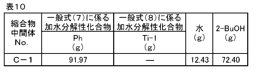
<縮合物中間体C-1の調製>
下記表10に記載の配合としたこと以外は、縮合物中間体-1と同様にして縮合物中間体C-1を調製した。なお、表10における記号「Ph」及び「Ti-1」は、各々表14に示す化合物を表す。 [Comparative Example 1]
<Preparation of condensate intermediate C-1>
A condensate intermediate C-1 was prepared in the same manner as the condensate intermediate-1 except that the formulation shown in Table 10 below was used. The symbols “Ph” and “Ti-1” in Table 10 represent the compounds shown in Table 14, respectively.
下記表11に記載の配合としたこと以外は、縮合物1-1と同様にして縮合物C-1を調製し、評価(1)に供した。結果を表11に併せて示す。なお、表11における記号「Ti-1」は、表14に示す化合物を表す。 <Preparation of condensate C-1>
A condensate C-1 was prepared in the same manner as the condensate 1-1 except that the formulation shown in Table 11 below was used, and was used for evaluation (1). The results are also shown in Table 11. The symbol “Ti-1” in Table 11 represents the compounds shown in Table 14.

縮合物C-1を用いたこと、及び、光カチオン重合開始剤を使用しなかったこと以外は、コーティング液1-1と同様にしてコーティング液C-1を調製した。 <Preparation of coating liquid C-1>
A coating liquid C-1 was prepared in the same manner as the coating liquid 1-1 except that the condensate C-1 was used and no photocationic polymerization initiator was used.
このコーティング液を用いたこと以外は、電子写真用部材1-1と同様にして電子写真用部材C-1を作製し、評価(2)~(3)に供した。 <Production and Evaluation of Electrophotographic Member C-1>
An electrophotographic member C-1 was produced in the same manner as the electrophotographic member 1-1 except that this coating solution was used, and was subjected to evaluations (2) to (3).
<縮合物C-2の調製>
下記表12に記載の配合としたこと以外は、縮合物1-1と同様にして縮合物C-2を調製し、評価(1)に供した。その結果を、表12に併せて示す。 [Comparative Example 2]
<Preparation of condensate C-2>
A condensate C-2 was prepared in the same manner as the condensate 1-1 except that the formulation shown in Table 12 below was used, and was used for evaluation (1). The results are also shown in Table 12.
縮合物C-2を用いたこと、及び、光カチオン重合開始剤を使用しなかったこと以外は、コーティング液1-1と同様にしてコーティング液C-2の調製を試みた。しかしながら、縮合物C-2に、白濁・沈殿が生じていたことから、均一なコーティング液を調製できなかった。そのため、評価(2)~(3)は実施しなかった。なお、表12における記号「Ph」及び「Ti-1」は、各々表14に示す化合物を表す。 <Preparation of coating liquid C-2>
An attempt was made to prepare the coating liquid C-2 in the same manner as the coating liquid 1-1 except that the condensate C-2 was used and that no photocationic polymerization initiator was used. However, a uniform coating solution could not be prepared due to white turbidity and precipitation in the condensate C-2. Therefore, evaluations (2) to (3) were not performed. The symbols “Ph” and “Ti-1” in Table 12 represent the compounds shown in Table 14, respectively.


102 導電性弾性層
103 表面層
1 感光体
2 軸
3 帯電部材
4 露光光
5 現像手段
6 転写ローラ
7 クリーニング手段
8 定着手段
9 プロセスカートリッジ
10 案内手段
P 転写材
20 表面電位計
21 感光体
22 帯電部材
23 露光手段
S1 帯電バイアス電源 DESCRIPTION OF
This application claims priority from Japanese Patent Application No. 2012-078170 filed on Mar. 29, 2012, the contents of which are incorporated herein by reference.
Claims (7)
- 導電性の基体と、弾性層と、表面層とを有する電子写真用部材の製造方法であって、
下記一般式(1)で示される加水分解性シラン化合物と、
下記一般式(2)で示されるキレートチタン化合物との加水分解縮合物を含む表面層形成用のコーティング液の塗膜を弾性層の表面に形成する第1の工程、及び、
該塗膜中の、該加水分解縮合物中のエポキシ基を開裂させることにより、該加水分解縮合物を架橋させて表面層を形成する第2の工程、を有することを特徴とする電子写真用部材の製造方法:


[一般式(1)中、R1は、下記一般式(3)~(6)のいずれかで示される炭化水素基を示す。また、R2~R4は、各々独立に炭化水素基を示す。
一般式(2)中、R5及びR6は各々独立に炭素数1~20の直鎖状又は分岐鎖状のアルキル基を表し、R7~R10は各々独立に水素原子、炭素数1~3のアルキル基または炭素数1~3のアルコキシ基を表す。


R14、R15、R19~R22、R27、R28、及びR33~R36は、各々独立に水素原子又は炭素数1~4のアルキル基を示す。
R25、R26、R31、及びR32は各々独立に水素原子、炭素数1~4のアルコキシル基又は炭素数1~4のアルキル基を示す。
n、m、l、q、s及びtは、各々独立に1~8の整数を示す。p及びrは、各々独立に4~12の整数を示す。また、「*」は、一般式(1)のケイ素原子との結合位置を示す。]]。 A method for producing an electrophotographic member having a conductive substrate, an elastic layer, and a surface layer,
A hydrolyzable silane compound represented by the following general formula (1);
A first step of forming, on the surface of the elastic layer, a coating film of a coating solution for forming a surface layer containing a hydrolysis condensate with a chelated titanium compound represented by the following general formula (2);
A second step of forming a surface layer by crosslinking the hydrolysis condensate by cleaving an epoxy group in the hydrolysis condensate in the coating film. Manufacturing method of member:
[In the general formula (1), R 1 represents a hydrocarbon group represented by any one of the following general formulas (3) to (6). R 2 to R 4 each independently represent a hydrocarbon group.
In the general formula (2), R 5 and R 6 each independently represents a linear or branched alkyl group having 1 to 20 carbon atoms, and R 7 to R 10 each independently represents a hydrogen atom or a carbon number of 1 Represents an alkyl group having ˜3 or an alkoxy group having 1 to 3 carbon atoms.
R 14 , R 15 , R 19 to R 22 , R 27 , R 28 , and R 33 to R 36 each independently represent a hydrogen atom or an alkyl group having 1 to 4 carbon atoms.
R 25 , R 26 , R 31 and R 32 each independently represent a hydrogen atom, an alkoxyl group having 1 to 4 carbon atoms or an alkyl group having 1 to 4 carbon atoms.
n, m, l, q, s and t each independently represent an integer of 1 to 8. p and r each independently represents an integer of 4 to 12. Further, “*” represents a bonding position with the silicon atom of the general formula (1). ]]. - 前記加水分解縮合物が、前記一般式(1)で示される加水分解性シラン化合物と、前記一般式(2)で示されるキレートチタン化合物と、下記一般式(7)で示される加水分解性シラン化合物との加水分解縮合物である請求項1に記載の電子写真用部材の製造方法:

- 前記加水分解縮合物が、前記一般式(1)で示される加水分解性シラン化合物と、前記一般式(2)で示されるキレートチタン化合物と、下記一般式(8)で示される加水分解性チタン化合物との加水分解縮合物である請求項1に記載の電子写真用部材の製造方法:

- 前記加水分解縮合物が、前記一般式(1)で示される加水分解性シラン化合物と、前記一般式(2)で示されるキレートチタン化合物と、下記一般式(7)で示される加水分解性シラン化合物と、下記一般式(8)で示される加水分解性チタン化合物との加水分解縮合物である請求項1に記載の電子写真用部材の製造方法。

- 前記一般式(2)で示されるキレートチタン化合物が、ジイソプロポキシチタンビス(アセチルアセトナート)又はジイソプロポキシチタンビス(エチルアセトアセテート)である請求項1~4のいずれか一項に記載の電子写真用部材の製造方法。 The electrophotography according to any one of claims 1 to 4, wherein the chelate titanium compound represented by the general formula (2) is diisopropoxy titanium bis (acetylacetonate) or diisopropoxy titanium bis (ethyl acetoacetate). Method for manufacturing a member.
- 下記一般式(1)で示される加水分解性シラン化合物と、下記一般式(2)で示されるキレートチタン化合物との加水分解縮合物を含むことを特徴とするポリシロキサンを含む膜の形成用のコーティング液:


[一般式(1)中、R1は、下記一般式(3)~(6)のいずれかで示される炭化水素基を示す。また、R2~R4は各々独立に炭化水素基を示す。
一般式(2)中、R5及びR6は各々独立に炭素数1~20の直鎖状又は分岐鎖状のアルキル基を表し、R7~R10は各々独立に水素原子、炭素数1~3のアルキル基または炭素数1~3のアルコキシ基を表す;


R14、R15、R19~R22、R27、R28、及びR33~R36は、各々独立に水素原子、又は炭素数1以上4以下のアルキル基を示す。
R25、R26、R31、及びR32は、各々独立に水素原子、炭素数1以上4以下のアルコキシル基、又は炭素数1以上4以下のアルキル基を示す。
n、m、l、q、s及びtは、各々独立に1以上8以下の整数を示す。p及びrは、各々独立に4以上12以下の整数を示す。また、「*」は、一般式(1)のケイ素原子との結合位置を示す。]]。 For forming a film containing polysiloxane, comprising a hydrolysis condensate of a hydrolyzable silane compound represented by the following general formula (1) and a chelate titanium compound represented by the following general formula (2): Coating liquid:
[In the general formula (1), R 1 represents a hydrocarbon group represented by any one of the following general formulas (3) to (6). R 2 to R 4 each independently represents a hydrocarbon group.
In the general formula (2), R 5 and R 6 each independently represent a linear or branched alkyl group having 1 to 20 carbon atoms, and R 7 to R 10 each independently represents a hydrogen atom or a carbon number of 1 Represents an alkyl group of ˜3 or an alkoxy group of 1 to 3 carbon atoms;
R 14 , R 15 , R 19 to R 22 , R 27 , R 28 , and R 33 to R 36 each independently represent a hydrogen atom or an alkyl group having 1 to 4 carbon atoms.
R 25 , R 26 , R 31 , and R 32 each independently represent a hydrogen atom, an alkoxyl group having 1 to 4 carbon atoms, or an alkyl group having 1 to 4 carbon atoms.
n, m, l, q, s, and t each independently represent an integer of 1 or more and 8 or less. p and r each independently represent an integer of 4 or more and 12 or less. Further, “*” represents a bonding position with the silicon atom of the general formula (1). ]]. - 前記一般式(2)で示されるキレートチタン化合物が、ジイソプロポキシチタンビス(アセチルアセトナート)又はジイソプロポキシチタンビス(エチルアセトアセテート)である請求項6に記載のコーティング液。 The coating liquid according to claim 6, wherein the chelate titanium compound represented by the general formula (2) is diisopropoxy titanium bis (acetylacetonate) or diisopropoxy titanium bis (ethyl acetoacetate).
Priority Applications (4)
| Application Number | Priority Date | Filing Date | Title |
|---|---|---|---|
| EP13770087.8A EP2833215B1 (en) | 2012-03-29 | 2013-03-15 | Method for manufacturing electrophotography member, and coating liquid |
| CN201380018308.2A CN104204961B (en) | 2012-03-29 | 2013-03-15 | The production method of electrophotography member and coating fluid |
| JP2013520662A JP6066906B2 (en) | 2012-03-29 | 2013-03-15 | Electrophotographic member manufacturing method and coating solution |
| US14/019,490 US9556359B2 (en) | 2012-03-29 | 2013-09-05 | Method of producing member for electrophotography |
Applications Claiming Priority (2)
| Application Number | Priority Date | Filing Date | Title |
|---|---|---|---|
| JP2012078170 | 2012-03-29 | ||
| JP2012-078170 | 2012-03-29 |
Related Child Applications (1)
| Application Number | Title | Priority Date | Filing Date |
|---|---|---|---|
| US14/019,490 Continuation US9556359B2 (en) | 2012-03-29 | 2013-09-05 | Method of producing member for electrophotography |
Publications (1)
| Publication Number | Publication Date |
|---|---|
| WO2013145616A1 true WO2013145616A1 (en) | 2013-10-03 |
Family
ID=49258930
Family Applications (1)
| Application Number | Title | Priority Date | Filing Date |
|---|---|---|---|
| PCT/JP2013/001779 WO2013145616A1 (en) | 2012-03-29 | 2013-03-15 | Method for manufacturing electrophotography member, and coating liquid |
Country Status (5)
| Country | Link |
|---|---|
| US (1) | US9556359B2 (en) |
| EP (1) | EP2833215B1 (en) |
| JP (1) | JP6066906B2 (en) |
| CN (1) | CN104204961B (en) |
| WO (1) | WO2013145616A1 (en) |
Cited By (3)
| Publication number | Priority date | Publication date | Assignee | Title |
|---|---|---|---|---|
| JP2015143850A (en) * | 2013-12-27 | 2015-08-06 | キヤノン株式会社 | Charging member, process cartridge, and electrophotographic image forming apparatus |
| JP2016200819A (en) * | 2015-04-10 | 2016-12-01 | キヤノン株式会社 | Charging member, process cartridge, and electrophotographic apparatus |
| JP2016224131A (en) * | 2015-05-27 | 2016-12-28 | キヤノン株式会社 | Charging member, process cartridge, and electrophotographic device |
Families Citing this family (27)
| Publication number | Priority date | Publication date | Assignee | Title |
|---|---|---|---|---|
| US9360789B1 (en) | 2014-11-28 | 2016-06-07 | Canon Kabushiki Kaisha | Member for electrophotography, process cartridge and image forming apparatus |
| US9442408B2 (en) | 2014-11-28 | 2016-09-13 | Canon Kabushiki Kaisha | Member for electrophotography, method for producing the same, and image forming apparatus |
| US9897931B2 (en) | 2014-11-28 | 2018-02-20 | Canon Kabushiki Kaisha | Electroconductive member for electrophotography, process cartridge, and electrophotographic image-forming apparatus |
| US9921513B2 (en) * | 2014-12-09 | 2018-03-20 | Canon Kabushiki Kaisha | Charging member, process cartridge, and electrophotographic apparatus |
| JP6415421B2 (en) * | 2014-12-26 | 2018-10-31 | キヤノン株式会社 | Electrophotographic member, process cartridge, and electrophotographic apparatus |
| US9989879B2 (en) | 2015-06-26 | 2018-06-05 | Canon Kabushiki Kaisha | Charging member, process cartridge and electrophotographic image forming apparatus |
| US9740133B2 (en) | 2015-09-30 | 2017-08-22 | Canon Kabushiki Kaisha | Charging member, process cartridge and electrophotographic image forming apparatus |
| US10678158B2 (en) | 2016-09-26 | 2020-06-09 | Canon Kabushiki Kaisha | Electro-conductive member for electrophotography, process cartridge, and electrophotographic image forming apparatus |
| JP6976774B2 (en) | 2016-09-27 | 2021-12-08 | キヤノン株式会社 | Conductive members for electrophotographic, process cartridges and electrophotographic image forming equipment |
| US10459356B2 (en) | 2016-10-07 | 2019-10-29 | Canon Kabushiki Kaisha | Charging member, process cartridge and electrophotographic image forming apparatus |
| US10416588B2 (en) | 2016-10-31 | 2019-09-17 | Canon Kabushiki Kaisha | Charging member, process cartridge, electrophotographic image forming apparatus, and method for manufacturing charging member |
| JP6784589B2 (en) | 2016-12-21 | 2020-11-11 | キヤノン株式会社 | Charging member, manufacturing method of charging member, process cartridge and electrophotographic image forming apparatus |
| US10248042B2 (en) | 2017-06-02 | 2019-04-02 | Canon Kabushiki Kaisha | Electrophotographic roller, process cartridge and electrophotographic apparatus |
| WO2019203227A1 (en) | 2018-04-18 | 2019-10-24 | キヤノン株式会社 | Conductive member, process cartridge, and image forming device |
| CN112020678B (en) | 2018-04-18 | 2022-11-01 | 佳能株式会社 | Conductive member, process cartridge, and electrophotographic image forming apparatus |
| WO2019203225A1 (en) | 2018-04-18 | 2019-10-24 | キヤノン株式会社 | Conductive member, process cartridge, and electrophotographic image forming device |
| CN112005173B (en) | 2018-04-18 | 2023-03-24 | 佳能株式会社 | Conductive member, process cartridge, and image forming apparatus |
| JP7336289B2 (en) | 2018-07-31 | 2023-08-31 | キヤノン株式会社 | Electrophotographic member, electrophotographic process cartridge and electrophotographic image forming apparatus |
| JP7114409B2 (en) | 2018-08-31 | 2022-08-08 | キヤノン株式会社 | Developing roller, electrophotographic process cartridge and electrophotographic image forming apparatus |
| US11169454B2 (en) | 2019-03-29 | 2021-11-09 | Canon Kabushiki Kaisha | Electrophotographic electro-conductive member, process cartridge, and electrophotographic image forming apparatus |
| JP7446878B2 (en) | 2019-03-29 | 2024-03-11 | キヤノン株式会社 | Conductive member, electrophotographic process cartridge, and electrophotographic image forming device |
| JP7330852B2 (en) | 2019-10-18 | 2023-08-22 | キヤノン株式会社 | Electrophotographic device, process cartridge, and cartridge set |
| JP7401255B2 (en) | 2019-10-18 | 2023-12-19 | キヤノン株式会社 | Electrophotographic equipment, process cartridges, and cartridge sets |
| JP7321884B2 (en) | 2019-10-18 | 2023-08-07 | キヤノン株式会社 | Electrophotographic device, process cartridge and cartridge set |
| JP7404026B2 (en) | 2019-10-18 | 2023-12-25 | キヤノン株式会社 | Electrophotographic equipment, process cartridges, and cartridge sets |
| JP7401256B2 (en) | 2019-10-18 | 2023-12-19 | キヤノン株式会社 | Electrophotographic equipment, process cartridges and cartridge sets |
| JP7330851B2 (en) | 2019-10-18 | 2023-08-22 | キヤノン株式会社 | Electrophotographic device, process cartridge, and cartridge set |
Citations (11)
| Publication number | Priority date | Publication date | Assignee | Title |
|---|---|---|---|---|
| JP2004258421A (en) * | 2003-02-26 | 2004-09-16 | Kanegafuchi Chem Ind Co Ltd | Conductive roller |
| JP2004359881A (en) * | 2003-06-06 | 2004-12-24 | Mitsubishi Chemicals Corp | Gas barrier coating agent composition and gas barrier laminated film |
| WO2005087882A1 (en) * | 2004-03-15 | 2005-09-22 | Tokuyama Corporation | Coating composition |
| JP2007004102A (en) * | 2004-09-02 | 2007-01-11 | Canon Inc | Charging member, process cartridge, and electrophotographic apparatus |
| JP2007047768A (en) * | 2005-07-14 | 2007-02-22 | Kaneka Corp | Conductive roller |
| JP2008299115A (en) * | 2007-05-31 | 2008-12-11 | Canon Inc | Charging member, process cartridge, and electrophotographic device |
| JP2010163584A (en) * | 2009-01-16 | 2010-07-29 | Kyushu Hi-Tech:Kk | Flexibility-imparting normal temperature curable inorganic coating agent for protection of chemical floor |
| JP2011154353A (en) | 2009-12-28 | 2011-08-11 | Canon Inc | Charging member, process cartridge and electrophotographic device |
| WO2012023270A1 (en) * | 2010-08-17 | 2012-02-23 | キヤノン株式会社 | Electrification member and manufacturing method for same |
| WO2012023241A1 (en) * | 2010-08-19 | 2012-02-23 | キヤノン株式会社 | Electrification member, process cartridge, and electrophotographic device |
| JP2012042936A (en) * | 2010-07-20 | 2012-03-01 | Canon Inc | Charging member, process cartridge and electrophotographic device |
Family Cites Families (33)
| Publication number | Priority date | Publication date | Assignee | Title |
|---|---|---|---|---|
| JP3812104B2 (en) * | 1997-12-02 | 2006-08-23 | Jsr株式会社 | Film forming composition |
| AU2002305019A1 (en) * | 2001-05-25 | 2002-12-09 | University Of British Columbia | Diagnostic methods for cardiovascular disease, low hdl-cholesterol levels, and high triglyceride levels |
| EP1359182A1 (en) * | 2002-05-03 | 2003-11-05 | SigmaKalon Group B.V. | Organo-functional polysiloxanes |
| US6967069B2 (en) * | 2003-04-09 | 2005-11-22 | Xerox Corporation | Photoconductive imaging members |
| JP2005029642A (en) * | 2003-07-09 | 2005-02-03 | Shin Etsu Chem Co Ltd | Silicone rubber coating agent composition |
| JP4508794B2 (en) * | 2004-09-14 | 2010-07-21 | 信越化学工業株式会社 | Antifouling condensation-curing organopolysiloxane composition and underwater structure |
| CN100570502C (en) * | 2004-12-28 | 2009-12-16 | 佳能株式会社 | Charging member, handle box and electronic photographing device |
| DE602005027749D1 (en) * | 2004-12-28 | 2011-06-09 | Canon Kk | CHARGER, PROCESS CARTRIDGE AND ELECTRIC PHOTOGRAPHIC DEVICE |
| KR100893985B1 (en) | 2004-12-28 | 2009-04-20 | 캐논 가부시끼가이샤 | Charging member, process cartridge and electrophotographic apparatus |
| KR101201135B1 (en) | 2006-02-28 | 2012-11-13 | 캐논 가부시끼가이샤 | Charging member, process cartridge, and electrophotographic apparatus |
| CN101395541B (en) | 2006-02-28 | 2012-01-18 | 佳能株式会社 | Charging member, process cartridge, and electrophotographic apparatus |
| JP5207682B2 (en) | 2006-09-29 | 2013-06-12 | キヤノン株式会社 | Developing member and electrophotographic image forming apparatus |
| JP5397350B2 (en) * | 2009-09-11 | 2014-01-22 | 信越化学工業株式会社 | Liquid silicone rubber coating composition, curtain airbag and method for producing the same |
| EP2453312B1 (en) | 2009-09-16 | 2016-09-14 | Canon Kabushiki Kaisha | Development roller, process cartridge, and electrophotographic image-forming device |
| JP4717959B1 (en) | 2009-12-14 | 2011-07-06 | キヤノン株式会社 | Charging member, process cartridge, and electrophotographic apparatus |
| JP5729988B2 (en) | 2009-12-15 | 2015-06-03 | キヤノン株式会社 | Charging member, process cartridge, and electrophotographic apparatus |
| WO2012020534A1 (en) | 2010-08-09 | 2012-02-16 | キヤノン株式会社 | Charging member, method for producing same, process cartridge, and electrophotographic device |
| EP2607960B1 (en) * | 2010-08-20 | 2018-01-03 | Canon Kabushiki Kaisha | Charging member |
| EP2624063B1 (en) * | 2010-09-27 | 2016-11-09 | Canon Kabushiki Kaisha | Electrification member, process cartridge, and electronic photographic device |
| JP4942233B2 (en) | 2010-09-27 | 2012-05-30 | キヤノン株式会社 | Charging member, process cartridge, and electrophotographic apparatus |
| WO2012042755A1 (en) | 2010-09-27 | 2012-04-05 | キヤノン株式会社 | Charging member, process cartridge and electrophotographic device |
| JP4954344B2 (en) | 2010-09-27 | 2012-06-13 | キヤノン株式会社 | Charging member and manufacturing method thereof |
| KR101521365B1 (en) * | 2010-09-30 | 2015-05-18 | 캐논 가부시끼가이샤 | Charging member, manufacturing method thereof, and electrophotographic apparatus |
| JP4902810B1 (en) | 2010-10-04 | 2012-03-21 | キヤノン株式会社 | Charging member, process cartridge, and electrophotographic apparatus |
| CN103282839B (en) | 2010-12-28 | 2015-10-14 | 佳能株式会社 | Developer roll, handle box and electronic photographing device |
| CN103380403B (en) | 2011-02-15 | 2015-06-10 | 佳能株式会社 | Charging member and process for production thereof, process cartridge, and electrophotographic device |
| EP2685318B1 (en) | 2011-03-09 | 2017-05-17 | Canon Kabushiki Kaisha | Charging member, process cartridge, and electrophotographic apparatus |
| EP2703901B1 (en) | 2011-04-25 | 2015-09-30 | Canon Kabushiki Kaisha | Charging member, process cartridge, and electronic photography device |
| CN103502894B (en) * | 2011-04-27 | 2015-11-25 | 佳能株式会社 | The production method of charging member, handle box, electronic photographing device and charging member |
| EP2703900B1 (en) | 2011-04-28 | 2015-09-23 | Canon Kabushiki Kaisha | Charging member, process cartridge and electrophotographic apparatus |
| KR101518661B1 (en) | 2011-04-28 | 2015-05-07 | 캐논 가부시끼가이샤 | Charging member, method for producing charging member, electrophotographic device, and processor cartridge |
| JP2012237823A (en) * | 2011-05-10 | 2012-12-06 | Konica Minolta Business Technologies Inc | Electrophotographic photoreceptor, process cartridge and image forming apparatus including the same |
| EP2771391B1 (en) * | 2011-10-27 | 2017-01-11 | Hewlett-Packard Indigo B.V. | Method of forming a release layer |
-
2013
- 2013-03-15 EP EP13770087.8A patent/EP2833215B1/en active Active
- 2013-03-15 CN CN201380018308.2A patent/CN104204961B/en active Active
- 2013-03-15 JP JP2013520662A patent/JP6066906B2/en active Active
- 2013-03-15 WO PCT/JP2013/001779 patent/WO2013145616A1/en active Application Filing
- 2013-09-05 US US14/019,490 patent/US9556359B2/en active Active
Patent Citations (11)
| Publication number | Priority date | Publication date | Assignee | Title |
|---|---|---|---|---|
| JP2004258421A (en) * | 2003-02-26 | 2004-09-16 | Kanegafuchi Chem Ind Co Ltd | Conductive roller |
| JP2004359881A (en) * | 2003-06-06 | 2004-12-24 | Mitsubishi Chemicals Corp | Gas barrier coating agent composition and gas barrier laminated film |
| WO2005087882A1 (en) * | 2004-03-15 | 2005-09-22 | Tokuyama Corporation | Coating composition |
| JP2007004102A (en) * | 2004-09-02 | 2007-01-11 | Canon Inc | Charging member, process cartridge, and electrophotographic apparatus |
| JP2007047768A (en) * | 2005-07-14 | 2007-02-22 | Kaneka Corp | Conductive roller |
| JP2008299115A (en) * | 2007-05-31 | 2008-12-11 | Canon Inc | Charging member, process cartridge, and electrophotographic device |
| JP2010163584A (en) * | 2009-01-16 | 2010-07-29 | Kyushu Hi-Tech:Kk | Flexibility-imparting normal temperature curable inorganic coating agent for protection of chemical floor |
| JP2011154353A (en) | 2009-12-28 | 2011-08-11 | Canon Inc | Charging member, process cartridge and electrophotographic device |
| JP2012042936A (en) * | 2010-07-20 | 2012-03-01 | Canon Inc | Charging member, process cartridge and electrophotographic device |
| WO2012023270A1 (en) * | 2010-08-17 | 2012-02-23 | キヤノン株式会社 | Electrification member and manufacturing method for same |
| WO2012023241A1 (en) * | 2010-08-19 | 2012-02-23 | キヤノン株式会社 | Electrification member, process cartridge, and electrophotographic device |
Cited By (3)
| Publication number | Priority date | Publication date | Assignee | Title |
|---|---|---|---|---|
| JP2015143850A (en) * | 2013-12-27 | 2015-08-06 | キヤノン株式会社 | Charging member, process cartridge, and electrophotographic image forming apparatus |
| JP2016200819A (en) * | 2015-04-10 | 2016-12-01 | キヤノン株式会社 | Charging member, process cartridge, and electrophotographic apparatus |
| JP2016224131A (en) * | 2015-05-27 | 2016-12-28 | キヤノン株式会社 | Charging member, process cartridge, and electrophotographic device |
Also Published As
| Publication number | Publication date |
|---|---|
| EP2833215A1 (en) | 2015-02-04 |
| EP2833215B1 (en) | 2019-06-19 |
| JP6066906B2 (en) | 2017-01-25 |
| CN104204961A (en) | 2014-12-10 |
| US20140004258A1 (en) | 2014-01-02 |
| US9556359B2 (en) | 2017-01-31 |
| JPWO2013145616A1 (en) | 2015-12-10 |
| EP2833215A4 (en) | 2015-10-28 |
| CN104204961B (en) | 2016-05-11 |
Similar Documents
| Publication | Publication Date | Title |
|---|---|---|
| JP6066906B2 (en) | Electrophotographic member manufacturing method and coating solution | |
| JP5038524B2 (en) | Charging member, process cartridge, and electrophotographic apparatus | |
| KR101469408B1 (en) | Charging member, process cartridge, and electronic photography device | |
| JP5943696B2 (en) | Charging member, method for manufacturing charging member, electrophotographic apparatus, and process cartridge | |
| KR101360617B1 (en) | Electrifying member, process cartridge, and electro-photographic device | |
| WO2013175734A1 (en) | Charging member, process cartridge, and electrophotographic device | |
| JP4878659B1 (en) | Charging member and electrophotographic apparatus | |
| JP4948668B2 (en) | Charging member, process cartridge, and electrophotographic apparatus | |
| WO2013183238A1 (en) | Charging member, process cartridge and electrophotographic apparatus | |
| WO2012147301A1 (en) | Charging member, process cartridge, electrophotographic device, and method for producing charging member | |
| JP6000989B2 (en) | Charging member and electrophotographic apparatus | |
| JP4841016B1 (en) | Charging member, process cartridge, and electrophotographic apparatus | |
| WO2012042765A1 (en) | Electrification member, process cartridge, and electronic photographic device | |
| WO2012023270A1 (en) | Electrification member and manufacturing method for same | |
| WO2012020534A1 (en) | Charging member, method for producing same, process cartridge, and electrophotographic device | |
| JP2009058634A (en) | Electrophotographic member, process cartridge and electrophotographic apparatus | |
| WO2012042781A1 (en) | Charging member and manufacturing method thereof | |
| JP5006586B2 (en) | Developing roller, manufacturing method thereof, developing apparatus, and electrophotographic process cartridge | |
| JP5279218B2 (en) | Charging member, process cartridge, and electrophotographic apparatus | |
| JP5213384B2 (en) | Charging member, process cartridge, and electrophotographic apparatus |
Legal Events
| Date | Code | Title | Description |
|---|---|---|---|
| WWE | Wipo information: entry into national phase |
Ref document number: 201380018308.2 Country of ref document: CN |
|
| ENP | Entry into the national phase |
Ref document number: 2013520662 Country of ref document: JP Kind code of ref document: A |
|
| 121 | Ep: the epo has been informed by wipo that ep was designated in this application |
Ref document number: 13770087 Country of ref document: EP Kind code of ref document: A1 |
|
| WWE | Wipo information: entry into national phase |
Ref document number: 2013770087 Country of ref document: EP |
|
| NENP | Non-entry into the national phase |
Ref country code: DE |