WO2013129010A1 - 送信回路 - Google Patents
送信回路 Download PDFInfo
- Publication number
- WO2013129010A1 WO2013129010A1 PCT/JP2013/051975 JP2013051975W WO2013129010A1 WO 2013129010 A1 WO2013129010 A1 WO 2013129010A1 JP 2013051975 W JP2013051975 W JP 2013051975W WO 2013129010 A1 WO2013129010 A1 WO 2013129010A1
- Authority
- WO
- WIPO (PCT)
- Prior art keywords
- circuit
- port
- transmission circuit
- input
- transmission
- Prior art date
- Legal status (The legal status is an assumption and is not a legal conclusion. Google has not performed a legal analysis and makes no representation as to the accuracy of the status listed.)
- Ceased
Links
Images


Classifications
-
- H—ELECTRICITY
- H04—ELECTRIC COMMUNICATION TECHNIQUE
- H04B—TRANSMISSION
- H04B1/00—Details of transmission systems, not covered by a single one of groups H04B3/00 - H04B13/00; Details of transmission systems not characterised by the medium used for transmission
- H04B1/02—Transmitters
- H04B1/04—Circuits
- H04B1/0458—Arrangements for matching and coupling between power amplifier and antenna or between amplifying stages
-
- H—ELECTRICITY
- H04—ELECTRIC COMMUNICATION TECHNIQUE
- H04B—TRANSMISSION
- H04B1/00—Details of transmission systems, not covered by a single one of groups H04B3/00 - H04B13/00; Details of transmission systems not characterised by the medium used for transmission
- H04B1/38—Transceivers, i.e. devices in which transmitter and receiver form a structural unit and in which at least one part is used for functions of transmitting and receiving
- H04B1/40—Circuits
- H04B1/50—Circuits using different frequencies for the two directions of communication
- H04B1/52—Hybrid arrangements, i.e. arrangements for transition from single-path two-direction transmission to single-direction transmission on each of two paths or vice versa
- H04B1/525—Hybrid arrangements, i.e. arrangements for transition from single-path two-direction transmission to single-direction transmission on each of two paths or vice versa with means for reducing leakage of transmitter signal into the receiver
Definitions
- the present invention relates to a transmission circuit, and more particularly to a transmission circuit incorporated in a portable wireless communication terminal.
- a transmission signal from a power amplifier is output to an antenna via a nonreciprocal circuit element (circulator or isolator) in a transmission circuit of a portable wireless communication terminal.
- the nonreciprocal circuit element has a characteristic (irreversible) that transmits a signal only in a predetermined specific direction and does not transmit in a reverse direction.
- the reflection characteristic from the antenna changes depending on the environmental condition, and a high frequency signal of about 25 to 50% in terms of voltage is reflected to the nonreciprocal circuit element (reverse direction input).
- Patent Document 1 proposes a wireless communication apparatus in which a phase shift unit is provided between the circulator and the antenna so that the phase of the reflected signal from the antenna and the phase of the transmission signal leaking from the isolator is increased, thereby increasing the recoverable power. Has been.
- the apparatus described in Patent Document 1 is not efficient when the recovered voltage is lower than the reference voltage because the recovered power is not used.
- the utilization efficiency is improved in the apparatus described in Patent Document 2, since it is configured as a circulator having three input / output ports, as in the apparatus described in Patent Document 1, there are many components, There is a problem that the communication circuit is enlarged.
- An object of the present invention is to provide a transmission circuit that can use a reflected wave from an antenna as power using a small two-port isolator.
- a transmission circuit is A two-port isolator that outputs a forward high-frequency signal input from an input port connected to the transmission side from an output port connected to the antenna side, and isolates a reverse high-frequency signal input from the output port
- a rectifier circuit provided in a portion in which a high-frequency signal in the forward direction of the two-port isolator hardly flows and a high-frequency signal in the reverse direction flows; It is provided with.
- the isolator provided in the transmission circuit is a small two-port type with a small number of parts, and outputs a high-frequency signal input from the input port to the antenna in the forward direction, and a reflected signal in the reverse direction is converted to direct current by the rectifier circuit. Rectify. Thereby, the isolation characteristic of the reflected signal in the reverse direction is ensured and the reflected signal is effectively used as power. For example, the rectified power is stored, boosted as necessary, and supplied to the main battery of the mobile phone. Alternatively, a cooling element of a heating element such as a power amplifier disposed in the vicinity of the transmission circuit is driven.
- a reflected wave from an antenna can be used as electric power using a small two-port isolator.
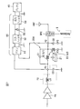
- FIG. 3 is an equivalent circuit diagram illustrating a transmission circuit according to the first embodiment.
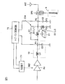
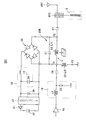
- FIG. 6 is an equivalent circuit diagram illustrating a transmission circuit according to a second embodiment. It is an equivalent circuit diagram which shows the transmission circuit which is 3rd Example. It is an equivalent circuit diagram which shows the transmission circuit which is 4th Example.
- FIG. 10 is an equivalent circuit diagram illustrating a transmission circuit according to a fifth embodiment. It is an equivalent circuit diagram which shows the transmission circuit which is 6th Example.
- the transmission circuit according to the first embodiment is configured as a transmission circuit of a mobile phone.
- a high-frequency signal (transmission signal) output from a power amplifier PA is passed through an isolator 20A and a duplexer DPX. It transmits to the antenna ANT, and includes an impedance matching circuit 10 with the power amplifier PA.
- the isolator 20A is provided with a rectifier circuit 30, which will be described in detail below.
- the power amplifier PA amplifies a transmission signal of a baseband IC (not shown).
- the impedance matching circuit 10 matches the output side impedance of the power amplifier PA with the input side impedance of the isolator 20A, and is formed as a matching circuit including an inductor L3 and a capacitor C3.
- the inductor L3 is connected in series between the output terminal of the power amplifier PA and the input port P1 of the isolator 20A.
- One end of the capacitor C3 is connected to the input port P1, and the other end is grounded.
- the duplexer DPX transmits a transmission signal to the antenna ANT and transmits a reception signal received by the antenna ANT to the reception circuit 5.
- the isolator 20A is a lumped constant type two-port type, and intersects the magnetic material for microwaves (hereinafter referred to as ferrite 21) to which a DC magnetic field is applied by a permanent magnet (not shown) and the ferrite 21 in an insulated state.
- the first center electrode 22 (inductor L1) and the second center electrode 23 (inductor L2) are provided.
- the first center electrode 22 has one end connected to the input port P1 and the other end connected to the output port P2.
- the second center electrode 23 has one end connected to the output port P2 and the other end connected to the ground port P3.
- a first matching capacitor C1 is connected between the input port P1 and the output port P2, and a second matching capacitor C2 is connected between the output port P2 and the ground port P3.
- the rectifier circuit 30 is configured as a diode bridge circuit including four diodes, and is connected in parallel with the first center electrode 22 and the capacitor C1 between the input port P1 and the output port P2.
- a smoothing circuit 35, a temporary storage circuit 36, and a booster circuit 37 are connected to the rectifier circuit 30, and the booster circuit 37 is connected to a main battery 40 of a mobile phone via a diode D1.
- the circuit 35 is configured as a smoothing circuit including an inductor L5 and a capacitor C5.
- the temporary power storage circuit 36 is a battery, and a capacitor or the like may be used.
- the booster circuit 37 is configured as a DC-DC converter.
- the ripple rectified by the smoothing circuit 35 is stored in the low-voltage temporary storage circuit 36 after being full-wave rectified by the rectifier circuit 30, and then boosted by the booster circuit 37 and supplied to the main battery 40.
- the diode D1 is for preventing a backflow from the main battery 40 to the booster circuit 37 (DD converter) and the temporary storage circuit 36.
- this transmission circuit is used by being incorporated in a cellular phone, when the impedance of the antenna ANT changes when a metal material comes close to the phone or touches or leaves the phone during use, the transmission signal is reflected from the antenna ANT. The degree to be increased. Such a reflected signal is isolated by the isolator 20A and is not transmitted to the power amplifier PA, but is also full-wave rectified by the rectifier circuit 30, and even a small reflected power is stored in the temporary power storage circuit 36 and efficiently. Used as energy.
- the 2-port isolator 20A has a smaller number of parts than the circulator and is small in size, and the rectifier circuit 30 and the like are compactly integrated, so that the entire transmission device can be downsized.
- the transmission circuit according to the second embodiment has a rectifier circuit constituted by a rectenna 50 and a battery 45 connected to the output section.
- the other configurations are the same as those of the first embodiment. Yes, the operational effects are basically the same as in the first embodiment.
- the rectenna 50 has a Schottky barrier diode D2 connected between an input filter 52 and an output filter 53 connected to the balun 51, and the diode D2 rectifies the input alternating current to direct current.
- the balun 51 is a balanced-unbalanced converter, and its input is connected to the ports P1 and P2.
- Input filter 52 blocks harmonics generated by diode D2.
- the rectenna is a rectifier circuit that receives radio waves (microwaves) and converts them into DC power, and has an RF-DC conversion efficiency of 80% or higher.
- the transmission circuit according to the third embodiment is constituted by a Cockcroft-Walton circuit 60 as a rectifier circuit, and a battery 45 is connected to the output section.
- the other configurations are the same as those of the first embodiment.
- the operational effects are basically the same as in the first embodiment.
- the Cockcroft-Wilton circuit 60 has a capacitor and a diode connected in a ladder shape, and its input section is connected to ports P1 and P2, and a DC voltage is applied to the output side capacitor sequentially. Is accumulated and boosted without switching.
- the transmission circuit according to the fourth embodiment uses a well-known RF-DC conversion circuit 65 as a rectifier circuit, its input section is connected to ports P1 and P2, and its output section is a power amplifier. It is connected to the power supply of the final stage transistor of PA.
- RF-DC conversion circuit 65 As shown in FIG. 4, the transmission circuit according to the fourth embodiment uses a well-known RF-DC conversion circuit 65 as a rectifier circuit, its input section is connected to ports P1 and P2, and its output section is a power amplifier. It is connected to the power supply of the final stage transistor of PA.
- Other configurations are the same as those of the first embodiment, and the operational effects are basically the same as those of the first embodiment.
- the transmission circuit according to the fifth embodiment uses a well-known AC-DC conversion circuit 70 as a rectifier circuit, its input section is connected to ports P1 and P2, and its output section is a cooling element. 71 is connected.
- AC-DC conversion circuit 70 as a rectifier circuit
- its input section is connected to ports P1 and P2
- its output section is a cooling element. 71 is connected.
- Other configurations are the same as those of the first embodiment.
- the cooling element 71 is disposed in the vicinity of the power amplifier PA, and the recovered power is supplied to the cooling element 71 to cool the power amplifier PA, the heating element can be cooled without requiring an extra power source.
- a Peltier element is suitable, and a fan or the like may be used.
- the cooling target may be another heating element such as a duplexer DPX.
- the transmission circuit according to the sixth embodiment basically has the same configuration as that of the first embodiment except that an isolator 20B shown in FIG. 6 is used as a two-port isolator.
- the first center electrode 22 has one end connected to the input port P1 and the other end connected to the output port P2.
- the second center electrode 23 has one end connected to the input port P1 and the other end connected to the ground port P3. Further, impedance matching capacitors C6 and C7 are connected to the input port P1 side and the output port P2 side, respectively.
- the isolator 20B by setting the inductance of the second center electrode 23 to be larger than the inductance of the first center electrode 22, when a high frequency signal is input from the input port P1 (forward input), the gyrator operation is performed. Both ends of the first center electrode 22 are at the same potential, so that almost no current flows through the first center electrode 22 and the rectifier circuit 30, and the input signal is output to the output port P2.
- a high frequency signal reflected signal
- the parallel resonance circuit and the rectifier circuit 30 formed by the first center electrode 22 and the capacitor C1. And converted into voltage by the rectifier circuit 30.
- the operational effect of the rectifier circuit 30 is as described in the first embodiment.
- the transmission circuit according to the present invention is not limited to the above embodiment, and can be variously modified within the scope of the gist thereof.
- the rectifier circuit 30, the smoothing circuit 35, the temporary storage circuit 36, the booster circuit 37, and the like can have various configurations.
- the present invention is useful for a transmission circuit incorporated in a portable wireless communication terminal or the like, and is particularly excellent in that a reflected wave from an antenna can be effectively used as power.
Landscapes
- Engineering & Computer Science (AREA)
- Computer Networks & Wireless Communication (AREA)
- Signal Processing (AREA)
- Transmitters (AREA)
Description
本発明は、送信回路、特に、携帯無線通信端末に組み込まれる送信回路に関する。
従来、携帯無線通信端末の送信回路にはパワーアンプからの送信信号を非可逆回路素子(サーキュレータやアイソレータ)を介してアンテナへ出力している。非可逆回路素子は、予め定められた特定方向にのみ信号を伝送し、逆方向には伝送しない特性(非可逆性)を有している。
ところで、携帯無線通信端末においては、環境条件によってアンテナからの反射特性が変化し、電圧換算で25~50%程度の高周波信号が非可逆回路素子に反射してくる(逆方向入力)。
そこで、反射信号の有効利用を図るため、特許文献1では、アンテナからの反射信号をサーキュレータを介して回収部に供給して直流に変換し、該直流電圧が参照電圧よりも高い場合には、予め定めた回路部品に供給するようにした無線通信装置が提案されている。また、特許文献2では、サーキュレータとアンテナとの間に移相部を設け、アンテナからの反射信号とアイソレータから漏れる送信信号との位相を揃えることにより、回収できる電力を大きくした無線通信装置が提案されている。
しかしながら、特許文献1に記載の装置では、回収電圧が参照電圧よりも低い場合、回収された電力は利用されることはないので、効率的ではない。特許文献2に記載の装置では、利用効率が改善されてはいるが、特許文献1に記載の装置と同様に、三つの入出力ポートを有するサーキュレータとして構成されているため、構成部品が多く、通信回路が大型化するという問題点を有している。
一方、小型で挿入損失特性のよい2ポート型のアイソレータが、例えば、特許文献3に記載されている。この種の2ポート型アイソレータでは、アンテナからの反射波を終端抵抗で熱として消費することで、アイソレーション特性を確保している。しかし、反射波を熱として拡散してしまうことは無駄でもある。
本発明の目的は、小型の2ポート型アイソレータを用いてアンテナからの反射波を電力として利用することができる送信回路を提供することにある。
本発明の一形態である送信回路は、
送信側に接続された入力ポートから入力された順方向の高周波信号をアンテナ側に接続された出力ポートから出力し、該出力ポートから入力された逆方向の高周波信号をアイソレーションする2ポート型アイソレータと、
前記2ポート型アイソレータの順方向の高周波信号がほとんど流れることがなく、かつ、逆方向の高周波信号が流れ込む部分に設けられた整流回路と、
を備えたことを特徴とする。
送信側に接続された入力ポートから入力された順方向の高周波信号をアンテナ側に接続された出力ポートから出力し、該出力ポートから入力された逆方向の高周波信号をアイソレーションする2ポート型アイソレータと、
前記2ポート型アイソレータの順方向の高周波信号がほとんど流れることがなく、かつ、逆方向の高周波信号が流れ込む部分に設けられた整流回路と、
を備えたことを特徴とする。
前記送信回路に設けたアイソレータは、部品点数の少ない小型の2ポート型であって、入力ポートから入力された高周波信号をアンテナに順方向に出力し、逆方向の反射信号を整流回路で直流に整流する。これにて、逆方向の反射信号のアイソレーション特性が確保されるとともに、反射信号が電力として有効利用される。例えば、整流された電力を蓄電して、必要に応じて昇圧して携帯電話機のメインバッテリに供給する。あるいは、送信回路の近傍に配置されたパワーアンプなどの発熱体の冷却素子を駆動する。
本発明によれば、小型の2ポート型アイソレータを用いてアンテナからの反射波を電力として利用することができる。
以下、本発明に係る送信回路の実施例について添付図面を参照して説明する。なお、各図において、同じ部材、部分については共通する符号を付し、重複する説明は省略する。
(第1実施例、図1参照)
第1実施例である送信回路は、携帯電話機の送信回路として構成されており、図1に示すように、パワーアンプPAから出力された高周波信号(送信信号)をアイソレータ20A及びデュプレクサDPXを介してアンテナANTに伝送するもので、パワーアンプPAとのインピーダンスマッチング回路10を備えている。アイソレータ20Aには整流回路30が設けられており、該整流回路30については以下に詳述する。
第1実施例である送信回路は、携帯電話機の送信回路として構成されており、図1に示すように、パワーアンプPAから出力された高周波信号(送信信号)をアイソレータ20A及びデュプレクサDPXを介してアンテナANTに伝送するもので、パワーアンプPAとのインピーダンスマッチング回路10を備えている。アイソレータ20Aには整流回路30が設けられており、該整流回路30については以下に詳述する。
パワーアンプPAはベースバンドIC(図示せず)の送信信号を増幅するものである。インピーダンスマッチング回路10は、パワーアンプPAの出力側インピーダンスをアイソレータ20Aの入力側インピーダンスに整合させるものであり、インダクタL3とコンデンサC3とからなる整合回路として形成されている。インダクタL3はパワーアンプPAの出力端子とアイソレータ20Aの入力ポートP1との間に直列に接続されている。コンデンサC3は一端が入力ポートP1に接続され、他端がグランドに落とされている。また、デュプレクサDPXは送信信号をアンテナANTに伝送するとともに、アンテナANTで受信した受信信号を受信回路5に伝送する。
アイソレータ20Aは、集中定数型の2ポートタイプであり、図示しない永久磁石により直流磁界が印加されるマイクロ波用磁性体(以下、フェライト21と称する)と、該フェライト21に互いに絶縁状態で交差して配置された第1中心電極22(インダクタL1)及び第2中心電極23(インダクタL2)とを備えている。第1中心電極22は、一端が入力ポートP1に接続され、他端が出力ポートP2に接続されている。第2中心電極23は、一端が出力ポートP2に接続され、他端がグランドポートP3に接続されている。入力ポートP1と出力ポートP2との間に、第1整合用コンデンサC1が接続され、出力ポートP2とグランドポートP3との間に第2整合用コンデンサC2が接続されている。
整流回路30は、4個のダイオードからなるダイオードブリッジ回路として構成されており、入力ポートP1と出力ポートP2との間に、第1中心電極22及びコンデンサC1と並列に接続されている。この整流回路30には平滑回路35、一時蓄電回路36、昇圧回路37が接続され、かつ、昇圧回路37は携帯電話機のメインバッテリ40にダイオードD1を介して接続されている。
回路35は、インダクタL5とコンデンサC5とからなる平滑回路として構成されている。一時蓄電回路36はバッテリであり、コンデンサなどを用いてもよい。昇圧回路37はDC-DCコンバータとして構成されている。
このアイソレータ20Aにおいては、高周波信号(送信信号)が入力ポートP1から出力ポートP2へ流れる順方向動作時には、第2中心電極23に大きな高周波電流が流れ、整流回路30やコンデンサC1にはほとんど高周波電流が流れないため、小さな挿入損失で送信信号が伝送される。一方、出力ポートP2から高周波電流(アンテナANTからの反射信号)が入力されると、第1中心電極22とコンデンサC1とで形成される並列共振回路及び整流回路30によって減衰(アイソレーション)されるとともに、整流回路30によって電圧に変換される。
整流回路30によって全波整流された電圧は、平滑回路35によってリップルが平滑化され、低圧用の一時蓄電回路36に蓄えられ、その後、昇圧回路37で昇圧されてメインバッテリ40に供給される。ダイオードD1はメインバッテリ40から昇圧回路37(DDコンバータ)や、一時蓄電回路36への逆流を防ぐためのものである。
この送信回路は携帯電話機に組み込まれて使用されるため、使用時に電話機に金属材が近接したり、手が触れたり離れたりして、アンテナANTのインピーダンスが変化すると送信信号がアンテナANTから反射される度合いが大きくなる。このような反射信号はアイソレータ20Aによってアイソレーションされ、パワーアンプPAに伝送されないことは勿論、整流回路30によって全波整流され、小さな反射電力であっても一時蓄電回路36に蓄えられ、効率的にエネルギーとして利用される。また、2ポート型のアイソレータ20Aは、サーキュレータと比較して部品点数が少なく小型であり、整流回路30などもコンパクトにまとめられているため、送信装置全体の小型化を図ることができる。
(第2実施例、図2参照)
第2実施例である送信回路は、図2に示すように、整流回路をレクテナ50で構成し、出力部にバッテリ45を接続したものであり、他の構成は前記第1実施例と同様であり、作用効果も基本的に第1実施例と同様である。
第2実施例である送信回路は、図2に示すように、整流回路をレクテナ50で構成し、出力部にバッテリ45を接続したものであり、他の構成は前記第1実施例と同様であり、作用効果も基本的に第1実施例と同様である。
レクテナ50は、ここでは、バラン51に接続した入力フィルタ52と出力フィルタ53との間にショットキーバリアダイオードD2を接続したものであり、ダイオードD2は入力された交流を直流に整流する。バラン51は平衡-不平衡変換器であり、その入力部はポートP1,P2に接続されている。入力フィルタ52はダイオードD2で発生した高調波を阻止する。レクテナは電波(マイクロ波)を受け取り、直流電力に変換する整流回路そのものであり、RF-DC変換効率が80%以上の高率である。
(第3実施例、図3参照)
第3実施例である送信回路は、図3に示すように、整流回路としてコッククロフト・ウォルトン回路60で構成し、出力部にバッテリ45を接続したものであり、他の構成は前記第1実施例と同様であり、作用効果も基本的に第1実施例と同様である。
第3実施例である送信回路は、図3に示すように、整流回路としてコッククロフト・ウォルトン回路60で構成し、出力部にバッテリ45を接続したものであり、他の構成は前記第1実施例と同様であり、作用効果も基本的に第1実施例と同様である。
コッククロフト・ウィルトン回路60は、よく知られているように、コンデンサとダイオードを梯子状に接続したもので、入力部はポートP1,P2に接続されており、出力側のコンデンサに逐次的に直流電圧が蓄積されていき、スイッチングなしで昇圧していく。
(第4実施例、図4参照)
第4実施例である送信回路は、図4に示すように、整流回路として周知のRF-DC変換回路65を用い、その入力部はポートP1,P2に接続されており、出力部はパワーアンプPAの最終段トランジスタの電源に接続されている。他の構成は前記第1実施例と同様であり、作用効果も基本的に第1実施例と同様である。
第4実施例である送信回路は、図4に示すように、整流回路として周知のRF-DC変換回路65を用い、その入力部はポートP1,P2に接続されており、出力部はパワーアンプPAの最終段トランジスタの電源に接続されている。他の構成は前記第1実施例と同様であり、作用効果も基本的に第1実施例と同様である。
(第5実施例、図5参照)
第5実施例である送信回路は、図5に示すように、整流回路として周知のAC-DC変換回路70を用い、その入力部はポートP1,P2に接続されており、出力部は冷却素子71に接続されている。他の構成は前記第1実施例と同様である。
第5実施例である送信回路は、図5に示すように、整流回路として周知のAC-DC変換回路70を用い、その入力部はポートP1,P2に接続されており、出力部は冷却素子71に接続されている。他の構成は前記第1実施例と同様である。
ところで、パワーアンプPAの出力が大きいときは、回収される電力も多くなるが、パワーアンプPA自身の発熱も大きくなる。それゆえ、パワーアンプPAの近傍に冷却素子71を配置し、回収した電力を冷却素子71に供給してパワーアンプPAを冷却すれば、余分な電源を要することなく発熱体を冷却することができる。冷却素子71としては、ペルチェ素子が好適であり、ファンなどを用いてもよい。なお、冷却対象としては、デュプレクサDPXなど他の発熱体であってもよい。
(第6実施例、図6参照)
第6実施例である送信回路は、基本的には前記第1実施例と同様の構成からなり、異なるのは、2ポート型アイソレータとして図6に示すアイソレータ20Bを用いている点である。
第6実施例である送信回路は、基本的には前記第1実施例と同様の構成からなり、異なるのは、2ポート型アイソレータとして図6に示すアイソレータ20Bを用いている点である。
このアイソレータ20Bにおいて、第1中心電極22は、一端が入力ポートP1に接続され、他端が出力ポートP2に接続されている。第2中心電極23は、一端が入力ポートP1に接続され、他端がグランドポートP3に接続されている。また、入力ポートP1側及び出力ポートP2側には、それぞれ、インピーダンス整合用のコンデンサC6,C7が接続されている。
アイソレータ20Bにあっては、第2中心電極23のインダクタンスを第1中心電極22のインダクタンスよりも大きく設定することにより、入力ポートP1から高周波信号が入力(順方向入力)されると、ジャイレータ動作により第1中心電極22の両端が同電位となり、第1中心電極22や整流回路30にはほとんど電流が流れず、入力信号は出力ポートP2に出力される。一方、出力ポートP2から高周波信号(反射信号)が入力(逆方向入力)されると、第1中心電極22とコンデンサC1とで形成される並列共振回路及び整流回路30によって減衰(アイソレーション)されるとともに、整流回路30によって電圧に変換される。整流回路30の作用効果は前記第1実施例で説明したとおりである。
また、アイソレータ20Bを用いて、前記第2~第5実施例に示した構成の送信回路を構成することも可能である。
(他の実施例)
なお、本発明に係る送信回路は前記実施例に限定するものではなく、その要旨の範囲内で種々に変更することができる。
なお、本発明に係る送信回路は前記実施例に限定するものではなく、その要旨の範囲内で種々に変更することができる。
例えば、整流回路30、平滑回路35、一時蓄電回路36、昇圧回路37などは、種々の構成のものを採用することができる。
以上のように、本発明は、携帯無線通信端末などに組み込まれる送信回路に有用であり、特に、アンテナからの反射波を電力として有効に利用できる点で優れている。
20A,20B…アイソレータ
21…フェライト
22…第1中心電極
23…第2中心電極
30…整流回路
35…平滑回路
36…一時蓄電回路
37…昇圧回路
40…メインバッテリ
45…バッテリ
50…レクテナ
60…コッククロフト・ウィルトン回路
65…RF-DC変換回路
70…AC-DC変換回路
71…冷却素子
P1…入力ポート
P2…出力ポート
ANT…アンテナ
21…フェライト
22…第1中心電極
23…第2中心電極
30…整流回路
35…平滑回路
36…一時蓄電回路
37…昇圧回路
40…メインバッテリ
45…バッテリ
50…レクテナ
60…コッククロフト・ウィルトン回路
65…RF-DC変換回路
70…AC-DC変換回路
71…冷却素子
P1…入力ポート
P2…出力ポート
ANT…アンテナ
Claims (12)
- 送信側に接続された入力ポートから入力された順方向の高周波信号をアンテナ側に接続された出力ポートから出力し、該出力ポートから入力された逆方向の高周波信号をアイソレーションする2ポート型アイソレータと、
前記2ポート型アイソレータの順方向の高周波信号がほとんど流れることがなく、かつ、逆方向の高周波信号が流れ込む部分に設けられた整流回路と、
を備えたことを特徴とする送信回路。 - 前記整流回路はダイオードブリッジ回路として構成されていること、を特徴とする請求項1に記載の送信回路。
- 前記整流回路に、さらに平滑回路、一時蓄電回路が接続されていること、を特徴とする請求項2に記載の送信回路。
- 前記一時蓄電回路は、昇圧回路を介してメインバッテリに接続されていること、を特徴とする請求項3に記載の送信回路。
- 前記整流回路はレクテナとして構成されていること、を特徴とする請求項1に記載の送信回路。
- 前記整流回路はコッククロフト・ウォルトン回路として構成されていること、を特徴とする請求項1に記載の送信回路。
- 前記整流回路はRF-DC変換回路として構成されていること、を特徴とする請求項1に記載の送信回路。
- 前記整流回路はAC-DC変換回路として構成されていること、を特徴とする請求項1に記載の送信回路。
- 送信回路の入力側又は出力側に接続された発熱体の近傍に該発熱体の冷却素子が配置され、前記整流回路にて整流された電力を該冷却素子に供給すること、を特徴とする請求項1ないし請求項8のいずれかに記載の送信回路。
- 送信回路の入力側にはパワーアンプが接続され、前記整流回路にて整流された電力を該パワーアンプに供給すること、を特徴とする請求項1ないし請求項9のいずれかに記載の送信回路
- 前記2ポート型アイソレータは、
永久磁石により直流磁界が印加されるマイクロ波用磁性体と、
前記マイクロ波用磁性体に互いに絶縁状態で交差して配置された第1中心電極及び第2中心電極と、
を備え、
前記第1中心電極は、一端が前記入力ポートに接続され、他端が前記出力ポートに接続され、
前記第2中心電極は、一端が前記出力ポートに接続され、他端がグランドポートに接続され、
前記入力ポートと前記出力ポートとの間に第1整合容量が接続され、
前記出力ポートと前記グランドポートとの間に第2整合容量が電気的に接続され、
前記入力ポートと前記出力ポートとの間に前記整流回路が接続されていること、
を特徴とする請求項1ないし請求項10のいずれかに記載の送信回路。 - 前記2ポート型アイソレータは、
永久磁石により直流磁界が印加されるマイクロ波用磁性体と、
前記マイクロ波用磁性体に互いに絶縁状態で交差して配置された第1及び第2中心電極と、
を備え、
前記第1中心電極は、一端が前記入力ポートに接続され、他端が前記出力ポートに接続され、
前記第2中心電極は、一端が前記入力ポートに接続され、他端がグランドポートに接続され、
前記入力ポートと前記出力ポートとの間に第1整合容量が接続され、
前記入力ポートと前記出力ポートとの間に前記整流回路が接続されていること、
を特徴とする請求項1ないし請求項10のいずれかに記載の送信回路。
Applications Claiming Priority (2)
| Application Number | Priority Date | Filing Date | Title |
|---|---|---|---|
| JP2012043620 | 2012-02-29 | ||
| JP2012-043620 | 2012-02-29 |
Publications (1)
| Publication Number | Publication Date |
|---|---|
| WO2013129010A1 true WO2013129010A1 (ja) | 2013-09-06 |
Family
ID=49082214
Family Applications (1)
| Application Number | Title | Priority Date | Filing Date |
|---|---|---|---|
| PCT/JP2013/051975 Ceased WO2013129010A1 (ja) | 2012-02-29 | 2013-01-30 | 送信回路 |
Country Status (1)
| Country | Link |
|---|---|
| WO (1) | WO2013129010A1 (ja) |
Citations (6)
| Publication number | Priority date | Publication date | Assignee | Title |
|---|---|---|---|---|
| JPH05335811A (ja) * | 1992-03-30 | 1993-12-17 | Toshiba Corp | レクテナ装置 |
| JP2004215477A (ja) * | 2002-03-19 | 2004-07-29 | Takion Co Ltd | マイクロ波送電装置、マイクロ波受電装置及びマイクロ波送電法 |
| JP2005102143A (ja) * | 2003-09-04 | 2005-04-14 | Murata Mfg Co Ltd | 2ポート型アイソレータ、その特性調整方法および通信装置 |
| JP2008011635A (ja) * | 2006-06-29 | 2008-01-17 | Sony Corp | 昇圧回路およびicカード |
| JP2008259419A (ja) * | 2001-05-22 | 2008-10-23 | Shinko Electric Co Ltd | 非接触給電装置 |
| JP2008278097A (ja) * | 2007-04-27 | 2008-11-13 | Ntt Docomo Inc | 無線通信装置、無線通信装置の給電方法 |
-
2013
- 2013-01-30 WO PCT/JP2013/051975 patent/WO2013129010A1/ja not_active Ceased
Patent Citations (6)
| Publication number | Priority date | Publication date | Assignee | Title |
|---|---|---|---|---|
| JPH05335811A (ja) * | 1992-03-30 | 1993-12-17 | Toshiba Corp | レクテナ装置 |
| JP2008259419A (ja) * | 2001-05-22 | 2008-10-23 | Shinko Electric Co Ltd | 非接触給電装置 |
| JP2004215477A (ja) * | 2002-03-19 | 2004-07-29 | Takion Co Ltd | マイクロ波送電装置、マイクロ波受電装置及びマイクロ波送電法 |
| JP2005102143A (ja) * | 2003-09-04 | 2005-04-14 | Murata Mfg Co Ltd | 2ポート型アイソレータ、その特性調整方法および通信装置 |
| JP2008011635A (ja) * | 2006-06-29 | 2008-01-17 | Sony Corp | 昇圧回路およびicカード |
| JP2008278097A (ja) * | 2007-04-27 | 2008-11-13 | Ntt Docomo Inc | 無線通信装置、無線通信装置の給電方法 |
Similar Documents
| Publication | Publication Date | Title |
|---|---|---|
| TWI435509B (zh) | 無線電源接收裝置以及無線電源供應系統 | |
| KR101343706B1 (ko) | 무선 전력 송신을 위한 송신기들 | |
| Lu et al. | A high efficiency 3.3 kW loosely-coupled wireless power transfer system without magnetic material | |
| US10158254B2 (en) | Resonant coupling power transmission system, resonance type power transmission device, and resonance type power reception device | |
| CN103580300B (zh) | 接收器及执行接收器操作的方法 | |
| JP6308371B2 (ja) | 無線電力伝送装置 | |
| CN105556835A (zh) | 高效率电压模式d类拓朴结构 | |
| JP2008104295A (ja) | 非接触電源装置 | |
| CN107925272A (zh) | 用于减少的电磁干扰的具有阻抗反转滤波器的用于无线功率传送的整流器 | |
| US20170005532A1 (en) | Automatic matching circuit for high frequency rectification circuit | |
| US20160308398A1 (en) | Rectifying circuit for high-frequency power supply | |
| US9742307B2 (en) | Rectifying circuit for high-frequency power supply | |
| US9979315B2 (en) | Rectifying circuit for high-frequency power supply | |
| US20160285321A1 (en) | Rectifying circuit for high-frequency power supply | |
| WO2013129010A1 (ja) | 送信回路 | |
| EP3771070B1 (en) | Resonant rectifier circuit | |
| JP6188825B2 (ja) | 高周波電源用整流回路 | |
| JP2014135836A (ja) | 受電装置及び非接触電力伝送システム | |
| CN105051842A (zh) | 双模式无线功率接收器 |
Legal Events
| Date | Code | Title | Description |
|---|---|---|---|
| 121 | Ep: the epo has been informed by wipo that ep was designated in this application |
Ref document number: 13754529 Country of ref document: EP Kind code of ref document: A1 |
|
| NENP | Non-entry into the national phase |
Ref country code: DE |
|
| 122 | Ep: pct application non-entry in european phase |
Ref document number: 13754529 Country of ref document: EP Kind code of ref document: A1 |
|
| NENP | Non-entry into the national phase |
Ref country code: JP |