WO2013099366A1 - プラズマ処理装置 - Google Patents
プラズマ処理装置 Download PDFInfo
- Publication number
- WO2013099366A1 WO2013099366A1 PCT/JP2012/073332 JP2012073332W WO2013099366A1 WO 2013099366 A1 WO2013099366 A1 WO 2013099366A1 JP 2012073332 W JP2012073332 W JP 2012073332W WO 2013099366 A1 WO2013099366 A1 WO 2013099366A1
- Authority
- WO
- WIPO (PCT)
- Prior art keywords
- antenna
- plasma
- conductor
- antennas
- conductors
- Prior art date
- Legal status (The legal status is an assumption and is not a legal conclusion. Google has not performed a legal analysis and makes no representation as to the accuracy of the status listed.)
- Ceased
Links
Images












Classifications
-
- H—ELECTRICITY
- H01—ELECTRIC ELEMENTS
- H01J—ELECTRIC DISCHARGE TUBES OR DISCHARGE LAMPS
- H01J37/00—Discharge tubes with provision for introducing objects or material to be exposed to the discharge, e.g. for the purpose of examination or processing thereof
- H01J37/32—Gas-filled discharge tubes
- H01J37/32009—Arrangements for generation of plasma specially adapted for examination or treatment of objects, e.g. plasma sources
- H01J37/32082—Radio frequency generated discharge
- H01J37/321—Radio frequency generated discharge the radio frequency energy being inductively coupled to the plasma
- H01J37/3211—Antennas, e.g. particular shapes of coils
-
- H—ELECTRICITY
- H05—ELECTRIC TECHNIQUES NOT OTHERWISE PROVIDED FOR
- H05H—PLASMA TECHNIQUE; PRODUCTION OF ACCELERATED ELECTRICALLY-CHARGED PARTICLES OR OF NEUTRONS; PRODUCTION OR ACCELERATION OF NEUTRAL MOLECULAR OR ATOMIC BEAMS
- H05H1/00—Generating plasma; Handling plasma
- H05H1/24—Generating plasma
- H05H1/46—Generating plasma using applied electromagnetic fields, e.g. high frequency or microwave energy
-
- H—ELECTRICITY
- H05—ELECTRIC TECHNIQUES NOT OTHERWISE PROVIDED FOR
- H05H—PLASMA TECHNIQUE; PRODUCTION OF ACCELERATED ELECTRICALLY-CHARGED PARTICLES OR OF NEUTRONS; PRODUCTION OR ACCELERATION OF NEUTRAL MOLECULAR OR ATOMIC BEAMS
- H05H1/00—Generating plasma; Handling plasma
- H05H1/24—Generating plasma
- H05H1/46—Generating plasma using applied electromagnetic fields, e.g. high frequency or microwave energy
- H05H1/4645—Radiofrequency discharges
- H05H1/4652—Radiofrequency discharges using inductive coupling means, e.g. coils
Definitions
- the present invention relates to a plasma processing apparatus that performs processing such as film formation by plasma CVD, etching, ashing, sputtering, etc. on a substrate using plasma. More specifically, the present invention is generated by applying a high-frequency current to an antenna. The present invention relates to an inductively coupled plasma processing apparatus that generates plasma by an induced electric field and performs processing on a substrate using the plasma.
- This application relates to an invention for further improvement of Japanese Patent No. 4844697 (plasma processing apparatus).
- a capacitively coupled plasma processing apparatus that generates capacitively coupled plasma (abbreviated as CCP) and an inductively coupled type that generates inductively coupled plasma (abbreviated as ICP) Plasma processing apparatus.
- CCP capacitively coupled plasma
- ICP inductively coupled type that generates inductively coupled plasma
- the capacitively coupled plasma processing apparatus applies a high-frequency voltage between two parallel electrodes and generates plasma using a high-frequency electric field generated between the two electrodes.
- a high voltage is applied to the plasma to increase the plasma potential, and charged particles (for example, ions) in the plasma impinge on and collide with the substrate with high energy, so that they are formed on the substrate.
- charged particles for example, ions
- an inductively coupled plasma processing apparatus in simple terms, generates plasma by an induced electric field generated by flowing a high-frequency current through an antenna. There is an advantage that it can be lowered.
- Patent Document 1 discloses that a flat antenna is attached to an opening of a vacuum vessel via an insulating frame, and a high-frequency power source is connected between one end and the other end of the antenna.
- a plasma processing apparatus is described in which a high-frequency power is supplied to flow a high-frequency current, plasma is generated by an induced electric field generated thereby, and a substrate is processed using the plasma.
- an inductively coupled plasma processing apparatus when an antenna is lengthened to cope with a large substrate, the impedance (particularly inductance) of the antenna increases, thereby generating a large potential difference between both ends of the antenna.
- the present invention is an inductively coupled device that can reduce the effective inductance of the antenna to suppress the plasma potential, and can control the plasma density distribution in the longitudinal direction by the antenna.
- the main purpose is to provide a device.
- Another object is to make it possible to generate a plasma with a larger area and more uniform plasma density distribution in two dimensions.
- One of the plasma processing apparatuses according to the present invention generates plasma by generating an induction electric field in a vacuum vessel by flowing a high-frequency current through an antenna having a substantially straight planar shape, and uses the plasma to form a substrate.
- a reciprocating plasma processing apparatus for performing a treatment wherein the antenna is disposed close to each other in a direction in which a perpendicular standing on the surface of the substrate is expanded and contracted, and the high-frequency currents flow in opposite directions.
- the distance between the reciprocating conductors in the direction in which the perpendicular is expanded and contracted is relatively small at the center in the longitudinal direction of the antenna and relatively large at both ends.
- the vertical direction in which the vertical line standing on the surface of the substrate is expanded and contracted is called the vertical direction, and the direction intersecting the vertical line is called the horizontal direction. Accordingly, the vertical direction is not necessarily the vertical direction.
- the antennas are constituted by reciprocating conductors that are arranged close to each other in the vertical direction and in which high-frequency currents flow in opposite directions.
- the effective inductance of the antenna becomes smaller due to the inductance. Therefore, the potential of the antenna can be kept low, and the plasma potential can be kept low.
- the mutual inductance between the reciprocating conductors can be varied in the longitudinal direction of the antenna, so that the electromagnetic energy supplied from the antenna to the plasma is It can be changed in the longitudinal direction of the antenna. Therefore, the plasma density distribution in the longitudinal direction can be controlled by this antenna.
- the electromagnetic energy supplied to the plasma from each antenna by making the vertical spacing between the reciprocating conductors of each antenna relatively small at the center in the antenna longitudinal direction and relatively large at both ends, Since it can be relatively larger in the vicinity of both ends than in the vicinity of the central portion in the antenna longitudinal direction, the uniformity of the plasma density distribution in the longitudinal direction of each antenna can be improved.
- the length in the antenna longitudinal direction of the region having a small conductor interval in the central portion of each antenna is relatively large in the central antenna in the parallel arrangement direction of the plurality of antennas and relatively small in the antennas at both ends. Therefore, the electromagnetic energy supplied to the plasma from multiple antennas can be made relatively larger near both ends than near the center in the parallel arrangement direction of the antennas, so that the plasma density distribution in the parallel arrangement direction of multiple antennas The uniformity can be improved.
- Both of the above actions can improve the uniformity of the plasma density distribution in the longitudinal direction and the parallel arrangement direction of the antenna, that is, the uniformity of the two-dimensional plasma density distribution.
- the conductor intervals of the corresponding portions of each antenna can be changed to a plurality of antennas. May be relatively small in the central antenna in the parallel arrangement direction, and relatively large in the antennas at both ends.
- one of the first and second flat plate conductors arranged in parallel and close to each other is used as a forward path for high frequency current, and the other flat plate conductor is used as a return path for high frequency current. You may make it supply electric power in parallel.
- the antenna is constituted by reciprocating conductors that are arranged close to each other in the vertical direction and in which high-frequency currents flow in opposite directions.
- the effective inductance of the antenna is reduced. Therefore, the potential of the antenna can be kept low, and the plasma potential can be kept low. As a result, the energy of charged particles incident on the substrate from the plasma can be reduced. Thereby, for example, damage to the film formed on the substrate can be suppressed to a small level, and the film quality can be improved. Further, even when the antenna is lengthened, the plasma potential can be kept low by keeping the antenna potential low for the above reasons, so that it becomes easy to cope with the increase in size of the substrate by lengthening the antenna.
- the mutual inductance between the reciprocating conductors can be changed in the longitudinal direction of the antenna by changing the vertical distance between the reciprocating conductors in the longitudinal direction of the antenna.
- the electromagnetic energy supplied to can be varied in the longitudinal direction of the antenna. Therefore, the plasma density distribution in the longitudinal direction can be controlled by this antenna.
- the processing state of the substrate in the longitudinal direction of the antenna can be controlled.
- the film thickness distribution in the longitudinal direction of the antenna can be controlled.
- the antenna is constituted by reciprocating conductors that are arranged close to each other in the vertical direction and in which high-frequency currents flow in opposite directions, and the vertical spacing between the reciprocating conductors is determined by the antenna.
- the magnetic flux density in the vicinity of the lower part of the antenna due to the change in the distance between the reciprocating conductors is changed. Good controllability. Therefore, the controllability of electromagnetic energy supplied from the antenna to the plasma by changing the interval between the reciprocating conductors, and hence the controllability of the plasma density distribution are good.
- the electromagnetic energy supplied to the plasma from each antenna is reduced by making the vertical spacing between the reciprocating conductors of each antenna relatively small at the center in the antenna longitudinal direction and relatively large at both ends. Since it can be made relatively larger in the vicinity of both end portions than in the vicinity of the central portion in the antenna longitudinal direction, the uniformity of the plasma density distribution in the longitudinal direction of each antenna can be improved. In addition, the length in the antenna longitudinal direction of the region having a small conductor interval in the central portion of each antenna is relatively large in the central antenna in the parallel arrangement direction of the plurality of antennas and relatively small in the antennas at both ends.
- the electromagnetic energy supplied to the plasma from multiple antennas can be made relatively larger near both ends than near the center in the parallel arrangement direction of the antennas, so that the plasma density distribution in the parallel arrangement direction of multiple antennas
- the uniformity can be improved.
- the uniformity of the plasma density distribution in the longitudinal direction and the parallel arrangement direction of the antenna that is, the uniformity of the plasma density distribution in two dimensions can be improved.
- the uniformity of substrate processing in two dimensions can be improved, processing with good uniformity can be performed on a larger area substrate.
- a film having a good uniformity of film thickness distribution in the substrate surface can be formed on a substrate having a larger area.
- the length in the antenna longitudinal direction of the region having a small conductor interval in the central portion of each antenna is relatively large in the central antenna in the parallel arrangement direction of the plurality of antennas, and relatively long in the antennas at both ends.
- the distance between the conductors of each antenna corresponding to each other is made relatively small at the central antenna in the parallel arrangement direction of the plurality of antennas and relatively large at the antennas at both ends, so that the plasma from the plurality of antennas
- the electromagnetic energy supplied to the antenna can be made relatively greater near both ends than near the center in the antenna parallel arrangement direction, so that the uniformity of the plasma density distribution in the parallel arrangement direction of the plurality of antennas can be improved. it can.
- a film having a good uniformity of film thickness distribution in the substrate surface can be formed on a substrate having a larger area.
- one of the first and second flat-plate conductors arranged in parallel and close to each other is used as a high-frequency current outgoing path, and the other flat-plate conductor is used as a high-frequency current return path, and the plurality of antennas. Since the high-frequency power is supplied in parallel to each other, the high-frequency currents flowing through the first and second flat plate conductors flow in opposite directions while being close to each other. As a result, the mutual impedance between the first and second plate conductors decreases the inductance of both plate conductors, and therefore the high-frequency power loss in the first and second plate conductors decreases.
- the other end of the upper conductor constituting each antenna is connected to the high-frequency power source via the matching circuit through the first and second flat plate conductors, and the other end of the lower conductor is directly or directly connected to the capacitor. Therefore, the potential of the lower conductor is lower than the potential of the upper conductor. Since the lower conductor is located on the plasma side, the potential of the lower conductor is reflected more strongly in the plasma potential than the potential of the upper conductor, so that the potential of the lower conductor becomes lower as described above. As a result, the plasma potential can be kept lower. As a result, the effect of the above (a) of claim 1 or 2 by suppressing the plasma potential (that is, the energy of charged particles incident on the substrate from the plasma can be suppressed low, even when the antenna is lengthened. ) Can be further reduced.
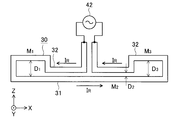
- FIG. 1A is a plan view
- FIG. 1B is a side view
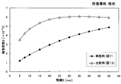
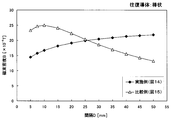
- 15 is a graph showing an example of a change in magnetic flux density with respect to a change in spacing in the case of the model shown in FIG. 14 (Example) and in the case of the model shown in FIG. 15 (Comparative Example).
- FIG. 10 is a schematic plan view showing still another example in which a plurality of antennas are arranged in parallel.
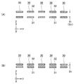
- 22A and 21B are cross sections along the Y direction of the antenna shown in FIG. 21, wherein FIG. 21A shows an AA cross section and a CC cross section, and FIG. 21B shows a BB cross section.
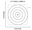
- FIG. It is a figure which shows the schematic example of two-dimensional plasma density distribution obtained when the well-known simple planar antenna long in X direction is arranged in multiple numbers in Y direction.
- FIG. 23 is a diagram showing a schematic example of a two-dimensional magnetic flux density distribution in the vicinity of the lower part of the antenna group obtained in the case of the example shown in FIG. 19 to FIG. 20 or FIG. 21 to FIG.
- FIG. 23 is a diagram showing a schematic example of a two-dimensional plasma density distribution obtained in the case of the example shown in FIG. 19-20 or FIG. 21-22.
- It is a schematic plan view which shows an example in the case of supplying a high frequency electric power to several antennas arranged in parallel through a parallel plate conductor. It is a perspective view which expands and shows the parallel plate conductor in FIG.
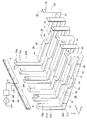
- FIG. 31 is a schematic perspective view showing an example of the periphery of a plurality of antennas that comprehensively adopt the technology described with reference to FIGS. 19 to 20, 26, 29, and 30, and the parallel plate conductors are shifted upward. Are shown.
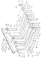
- FIG. 31 is a schematic perspective view showing an example around a plurality of antennas that comprehensively employs the technology described with reference to FIGS. 21 to 22, 26, 29, and 30, with the parallel plate conductors shifted upward; Are shown.
- FIG. 1 An embodiment of the plasma processing apparatus according to the present invention is shown in FIG. 1, and the antenna 30 is extracted and shown in FIG.
- the Z direction is a direction in which the perpendicular 3 standing on the surface of the substrate 2 is expanded and contracted
- the Y direction is a direction intersecting (for example, orthogonal to) the perpendicular 3, and these are for simplifying the expression as described above.
- These are referred to as the vertical direction Z and the horizontal direction Y, respectively.
- the X direction is a direction that intersects (for example, is orthogonal to) the perpendicular 3 and is a longitudinal direction of the antenna 30.
- the X direction and the Y direction are horizontal directions, but are not limited thereto. The same applies to the other drawings.
- This apparatus by generating an induced electric field in the vacuum vessel 4 to produce a plasma 50 by the induced electric field by the planar shape frequency current I R from the high frequency power source 42 in a substantially straight antenna 30, the plasma 50 is an inductively coupled plasma processing apparatus for processing the substrate 2 using 50.
- substantially straight means not only literally straight, but also includes a state that is almost straight (almost straight).
- the substrate 2 is, for example, a substrate for a flat panel display (FPD) such as a liquid crystal display or an organic EL display, a flexible substrate for a flexible display, a substrate for a semiconductor device such as a solar cell, or the like. is not.
- FPD flat panel display
- a flexible substrate for a flexible display a substrate for a semiconductor device such as a solar cell, or the like.
- the planar shape of the substrate 2 is, for example, a circle or a rectangle, and is not limited to a specific shape.
- the treatment applied to the substrate 2 is, for example, film formation by plasma CVD, etching, ashing, sputtering, or the like.
- This plasma processing apparatus is also called a plasma CVD apparatus when a film is formed by plasma CVD, a plasma etching apparatus when etching is performed, a plasma ashing apparatus when ashing is performed, and a plasma sputtering apparatus when sputtering is performed.
- This plasma processing apparatus includes, for example, a metal vacuum vessel 4 and the inside thereof is evacuated by a evacuation apparatus 8.
- a gas 24 is introduced into the vacuum vessel 4 through a gas introduction pipe 22.
- the gas 24 may be set according to the processing content applied to the substrate 2.
- the gas 24 is a source gas or a gas obtained by diluting it with a diluent gas (for example, H 2 ). More specifically, an Si film is formed on the surface of the substrate 2 when the source gas is SiH 4, an SiN film is formed when SiH 4 + NH 3 is used, and an SiO 2 film is formed when SiH 4 + O 2 is used. be able to.
- a holder 10 that holds the substrate 2 is provided in the vacuum vessel 4.
- the holder 10 is supported by the shaft 16.
- a bearing portion 18 having an electrical insulation function and a vacuum sealing function is provided at a portion where the shaft 16 penetrates the vacuum container 4.
- a negative bias voltage may be applied to the holder 10 from the bias power source 20 via the shaft 16.
- the bias voltage may be a negative pulse voltage. With such a bias voltage, for example, the energy when positive ions in the plasma 50 are incident on the substrate 2 can be controlled to control the crystallinity of the film formed on the surface of the substrate 2.
- the antenna 30 is provided in the opening 7 of the ceiling surface 6 of the vacuum vessel 4 with an insulating frame 38 interposed therebetween. Between these elements, a packing 40 for vacuum sealing is provided.
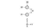
- the antenna 30 is composed of reciprocating conductors 31 and 32 arranged close to each other in the vertical direction Z.
- the planar shape of the antenna 30 (more specifically, the reciprocating conductors 31 and 32 constituting the antenna 30) is planar. More specifically, the planar shape is rectangular in this embodiment, but is not limited thereto. The antenna 30 will be described in detail later.
- the material of the antenna 30 is, for example, copper (more specifically, oxygen-free copper), aluminum, or the like, but is not limited thereto.
- high-frequency power is supplied to the antenna 30 from the high-frequency power source 42 via the matching circuit 44 to the reciprocating conductors 31 and 32, whereby a high-frequency current I R flows through the antenna 30. That is, the reciprocating conductors 31 and 32 constituting the antenna 30 opposite the high-frequency current (return current) I R is passed through each other (because the high frequency, the direction of the high-frequency current I R is inverted by the time. Hereinafter the same) .
- the high frequency current I R generates a high frequency magnetic field around the antenna 30, thereby generating an induction electric field in a direction opposite to the high frequency current I R.
- the high-frequency power source 42 has an output end 42 a and a ground end 42 b, and the output end 42 a is connected to one end of the conductor 31 through a matching circuit 44.
- the ground end 42b is grounded.
- One end of the conductor 32 is also grounded.
- the frequency of the high-frequency power output from the high-frequency power source 42 is, for example, a general 13.56 MHz, but is not limited thereto.
- the matching circuit 44 includes a capacitor 64 in series with a line and a capacitor 65 in parallel. Both capacitors 64 and 65 are variable in capacity in this example.
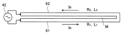
- the total impedance Z T of the parallel reciprocating conductors 61 and 62 that are close to each other is expressed by the following equation as described in the book of electrical theory as a differential connection.
- R 1 and L 1 are the resistance and self-inductance of one conductor 61, respectively
- R 2 and L 2 are the resistance and self-inductance of the other conductor 62
- M is between the two conductors 61 and 62, respectively.
- the mutual inductance M between the reciprocating conductors 61 and 62 is increased, total impedance Z T and the effective inductance L T is reduced.
- the electromagnetic energy G generated by flowing a high-frequency current I R from the high-frequency power source 42 to the reciprocating conductors 61 and 62 is expressed by the following equation. Therefore, when the mutual inductance M increases, the electromagnetic energy G decreases, The acting magnetic effect is reduced. In the case of plasma generation, the electromagnetic energy that can be supplied to the plasma decreases and the plasma density decreases. The reverse case is the opposite.
- the mutual inductance M is not uniform in the longitudinal direction of the reciprocating conductors 61 and 62, that is, when the mutual inductance M is changed (in other words, changed), if each region is viewed, Depending on the mutual inductance M, the effective inductance and electromagnetic energy are determined.
- the antenna 30 constituting the present invention applies the above principle.
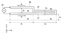
- the antenna 30 is configured by reciprocating conductors 31 and 32 arranged close to each other in the vertical direction Z, and the distance D in the vertical direction Z between the reciprocating conductors 31 and 32. and if is varied in two stages in the longitudinal direction X of the antenna 30, than the mutual inductance M 2 area a 2 of the small distance D 2, the direction of the mutual inductance M 1 area a 1 of the large distance D 1 (Ie, M 1 ⁇ M 2 ).
- the effective inductance of the area A 1 is larger than the area A 2 as can be seen by referring to the above equation 3, and the antenna 30 (more specifically, as can be seen from the description referring to the above equation 4).
- the magnetic flux density of the space at a distance H 1 from the conductor 31), than the magnetic flux density B 2 in the area a 2, towards the magnetic flux density B 1 in the area a 1 is greater (i.e. B 1> B 2) . Therefore, the plasma density in the region A 1 can be made larger than the plasma density in the region A 2 .
- the matching circuit 44 is omitted for the sake of simplification, but normally, as in the example shown in FIG. A matching circuit 44 is provided therebetween.
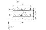
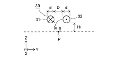
- the magnetic flux density B 0 in Table 1 is the magnetic flux density at the point P in the case of a known planar antenna having only the conductor 31 without the conductor 32.
- Table 1 shows the ratio B / B 0 and the square ratio (B / B 0 ) 2 between the magnetic flux density B 0 in that case and the magnetic flux density in the case of the reciprocating conductors 31 and 32.
- the reason for paying attention to the square ratio (B / B 0 ) 2 is that the supply of electromagnetic energy to the plasma is approximately proportional to the square of the magnetic flux density B, like eddy current loss.
- the magnetic flux density B and the square ratio (B / B 0 ) 2 can be greatly changed. For example, when the distance D is 1 mm and 50 mm, a difference of about 60 times can be added to the square ratio (B / B 0 ) 2 .
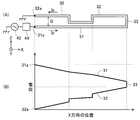
- FIG. 8 shows that the distance D in the vertical direction Z between the reciprocating conductors 31 and 32 arranged close to each other in the vertical direction Z is larger than the distance D 2 in the central region A 2 in the longitudinal direction X of the antenna 30.
- the distance D in the vertical direction Z between the reciprocating conductors 31 and 32 is relatively small in the central area A 2 in the longitudinal direction X of the antenna 30 (the distance is D 2 ).
- the antenna 30 shown in FIGS. 1 and 2 corresponds to the antenna 30 shown in FIG. 8 and is a more specific example.
- the antenna 30 shown in FIGS. 1 and 2 will be described in detail.
- the antenna 30 has reciprocating conductors 31 and 32 arranged close to each other with a distance D in the vertical direction Z. Both the conductors 31 and 32 are plate-shaped, and the planar shape thereof is a rectangle as described above.
- the lower surface of the conductor 31 on the lower side (plasma 50 side) is located in the vacuum atmosphere in the vacuum vessel 4, and the upper conductor 32 is located in the atmosphere.
- One end of each of the conductors 31 and 32 is electrically open, and an insulator 36 is provided there in this example.
- the other end portions are electrically connected to each other at the connection portion 33.
- High-frequency power is supplied from one high-frequency power source 42 via a matching circuit 44 between one end portions of both the conductors 31 and 32.
- Both conductors 31 and 32 have a plate shape in this example (specifically, the conductor 31 has a flat plate shape and the conductor 32 has a bent plate shape).
- the thickness of the lower conductor 31 may be increased as in the example shown in FIGS. 1 and 2C, or the thickness of both the conductors 31 and 32 as in the example shown in FIG. The sizes may be similar to each other.
- the electromagnetic energy supplied from the antenna 30 to the plasma 50 can be made relatively larger at both end portions than at the central portion in the longitudinal direction X of the antenna 30.
- the distance D and the mutual inductance M of the antenna 30 may be changed stepwise in the longitudinal direction X of the antenna 30 as in the examples shown in FIGS. 1 and 8 or may be changed continuously. .
- the plasma density can be smoothly changed because the plasma has a diffusing action.
- the upper conductor 32 shown in FIGS. 1 and 2 is formed in a gentle valley shape with a depressed central portion, and the distance D and the mutual inductance M of the antenna 30 are continuously changed in the longitudinal direction X of the antenna 30. You may let them.
- the antenna 30 shown in FIGS. 1, 2, and 8 may be provided. Furthermore, you may provide the antenna 30 of the other structure shown in FIG. 6 may be provided.
- the example shown in FIG. 9 is a modification of the example shown in FIGS. That is, instead of supplying high-frequency power from the end of the antenna 30 as shown in FIGS. 1 and 8 (end feeding), high-frequency power is supplied from the center of the antenna 30 as shown in FIG. (Central feeding) may be used. Similarly, in the antenna 30 of another example, the central feeding may be used.
- the reciprocating conductors 31 and 32 constituting the antenna 30 may have a plate shape as in the above-described example, a rod shape as in the example shown in FIG. 10, or a combination of a plate shape and a rod shape, for example. good.
- the lower conductor 31 may be plate-shaped and the upper conductor 32 may be rod-shaped.
- the upper bar-like conductors 32 may be formed in a plurality (two in FIG. 12) that are electrically parallel to each other.
- the reciprocating conductors 31 and 32 are electrically connected to each other at the end portion in the longitudinal direction X at the connection portion (see the connection portion 33 in FIG. 1).
- each of the conductors 31 and 32 is not limited to the illustrated example, and may be a circle, an ellipse, a rectangle, or the like. Alternatively, a structure may be adopted in which the conductors 31 and 32 are made hollow and a coolant such as cooling water is passed therethrough to forcibly cool the conductors 31 and 32.
- the antenna 30 is constituted by the reciprocating conductors 31 and 32 that are arranged close to each other in the vertical direction Z and in which the high-frequency currents I R flow in opposite directions.
- the effective inductance of the antenna 30 is reduced by the mutual inductance between the reciprocating conductors 31 and 32. Since the impedance of the antenna 30 is mostly an inductance in the high frequency region, the effective inductance is reduced, so that the potential difference generated in the antenna 30 is reduced, the potential of the antenna 30 is reduced, and the potential of the plasma 50 is reduced. Can be suppressed.
- the energy of charged particles (for example, ions) incident on the substrate 2 from the plasma 50 can be kept small.
- damage to the film can be suppressed to be small, and the film quality can be improved.
- the plasma potential can be kept low by keeping the potential of the antenna 30 low for the above reasons. Therefore, it is easy to cope with the increase in size of the substrate 2 by lengthening the antenna 30. Become.
- the mutual inductance M between the reciprocating conductors 31 and 32 can be changed in the longitudinal direction X of the antenna 30 by changing the distance D in the vertical direction Z between the reciprocating conductors 31 and 32 in the longitudinal direction X of the antenna. Therefore, the electromagnetic energy supplied from the antenna 30 to the plasma 50 can be changed in the longitudinal direction X of the antenna 30. Therefore, the plasma density distribution in the longitudinal direction X can be controlled by the antenna 30. As a result, the substrate processing state in the longitudinal direction X of the antenna 30 can be controlled. For example, when a film is formed on the substrate 2 by the plasma 50, the film thickness distribution in the longitudinal direction X of the antenna 30 can be controlled.
- the antenna 30 is configured by reciprocating conductors 31 and 32 that are arranged close to each other in the vertical direction Z and in which the high-frequency currents I R flow in opposite directions, and the vertical direction Z between the reciprocating conductors 31 and 32. Since the distance D between the reciprocating conductors 31 and 32 is changed in the longitudinal direction X of the antenna 30 as compared with the case where the distance in the left and right direction Y between the reciprocating conductors arranged close to each other in the left and right direction is changed. The controllability of the magnetic flux density in the vicinity of the lower part of the antenna 30 due to the change in the distance D is good. Therefore, the controllability of the electromagnetic energy supplied from the antenna 30 to the plasma 50 and the controllability of the plasma density distribution by changing the distance D between the reciprocating conductors 31 and 32 are good. This will be described below based on the simulation result.
- FIG. 7 shows an example of the change in the magnetic flux density B at the point P when the distance D in the vertical direction Z between the reciprocating conductors 31 and 32 is changed.
- the calculation conditions at this time are the same as those explained in the explanation part of FIG. 7, and this embodiment is the same as the magnetic flux density B in Table 1.
- FIG. 16 shows a change of the magnetic flux density B at the point P when the distance D in the left-right direction Y is changed.
- the calculation conditions at this time are such that the thickness T of both conductors 31 and 32 is 70 mm, the width W in the left-right direction Y is 3 mm, and other distances H 1 and the magnitude of the high-frequency current I R are the same as in FIG. I made it.
- the control of the magnetic flux density B is better in the example than in the comparative example. That is, by changing the distance D, the magnetic flux density B is controlled, thereby controlling the electromagnetic energy supplied from the antenna 30 to the plasma, and thus controlling the plasma density distribution.
- FIG. 17 shows an example of a change in the magnetic flux density B at the point P when the distance D in the vertical direction Z between the reciprocating conductors 31 and 32 is changed.
- the calculation conditions at this time were such that the diameter d of the two conductors 31 and 32 was 6 mm, and the other distance H 1 , the magnitude of the high-frequency current I R , and the like were the same as in FIG.
- FIG. 15 shows a change in the magnetic flux density B at the point P when the distance D in the left-right direction Y is changed.
- the calculation conditions at this time were the same as those in FIG. 14 except that the arrangement of the two conductors 31 and 32 was changed as described above.
- the magnetic flux density B changes once and then decreases, whereas in the case of the example, The magnetic flux density B changes gently in a nearly proportional state. Therefore, also in this case, the control of the magnetic flux density B is better in the example than in the comparative example. That is, by changing the distance D, the magnetic flux density B is controlled, thereby controlling the electromagnetic energy supplied from the antenna 30 to the plasma, and thus controlling the plasma density distribution.
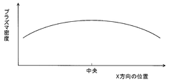
- the plasma density distribution in the longitudinal direction X is smaller than the plasma density at the center part as shown in FIG. 4, for example. It becomes a mountain-shaped distribution. The reason for this will be briefly explained.
- the plasma diffuses from the left and right sides in the central portion, whereas the plasma diffuses only from one side at both ends.
- the distance D in the vertical direction Z between the reciprocating conductors 31, 32 is larger than the distance between the central portions in the longitudinal direction X of the antenna 30.
- the distance D in the vertical direction Z between the reciprocating conductors 31 and 32 is relatively small at the center in the longitudinal direction X of the antenna 30 and relatively at both ends.
- the mutual inductance at both ends can be made smaller than the center in the longitudinal direction X of the antenna 30, so that the effective inductance at both ends relative to the center of the antenna 30 is relative to the center as described above. Become bigger.
- the electromagnetic energy supplied from the antenna 30 to the plasma 50 is made relatively larger near both ends than near the center in the longitudinal direction X of the antenna 30, contrary to the mountain shape, and more than near the center. Since the plasma 50 can be generated more strongly in the vicinity of both ends, the above-mentioned peak-shaped plasma density distribution can be corrected, and the uniformity of the plasma density distribution in the longitudinal direction X of the antenna 30 can be improved. As a result, the uniformity of substrate processing in the longitudinal direction of the antenna 30 can be improved. For example, when a film is formed on the substrate 2 by the plasma 50, the uniformity of the film thickness distribution in the longitudinal direction X of the antenna 30 can be improved.
- the shielding board 46 which shields the surface inside the vacuum vessel 4 of the antenna 30 from the plasma 50 like embodiment shown in FIG.
- the shielding plate 46 is made of an insulating material.
- the shielding plate 46 may be attached directly near the entrance of the opening 7 of the ceiling surface 6 of the vacuum vessel 4 or may be attached using a frame-like support plate 48 as in this embodiment. Even when the antenna 30 other than the example shown in FIG. 1 is used, such a shielding plate 46 may be provided.
- the material of the shielding plate 46 is, for example, quartz, alumina, silicon carbide, silicon or the like. If it is difficult to reduce oxygen by hydrogen plasma and release oxygen from the shielding plate 46, a non-oxide material such as silicon or silicon carbide may be used. For example, it is easy to use a silicon plate.
- the shielding plate 46 is provided, the surface of the antenna 30 or the like is sputtered by charged particles (mainly ions) in the plasma 50, and metal contamination (metal contamination) occurs in the plasma 50 and the substrate 2. Occurrence can be prevented.
- the shielding plate 46 is provided, the shielding plate is made of an insulating material and cannot prevent the potential of the antenna 30 from reaching the plasma 50. Therefore, as described above, the effective inductance of the antenna 30 is reduced to reduce the antenna 30. It is effective to keep the potential of ⁇ ⁇ low.
- a plurality of the antennas 30 having the above-described configuration may be arranged in parallel in the Y direction, and high frequency power may be supplied in parallel to each antenna 30 from a common high frequency power source 42. . Further, as shown in the figure, high frequency power may be supplied in parallel from a common high frequency power source 42 to the plurality of antennas 30 via variable impedances 52 connected in series to the respective antennas 30.
- Each antenna 30 may have any of the configurations described above with reference to FIG. 1, FIG. 2, FIG. 6, FIG. The antenna 30 of each example described later may be used.
- the variable impedance 52 may be a variable inductance as shown in FIG. 18, a variable capacitor (variable capacitance), or a mixture of both.
- a variable capacitor variable capacitance
- By inserting the variable inductance it is possible to increase the impedance of the power feeding circuit, and thus it is possible to suppress the current of the antenna 30 through which a high-frequency current flows excessively.
- By inserting a variable capacitor when the inductive reactance is large, the capacitive reactance can be increased and the impedance of the power feeding circuit can be decreased. Therefore, the current of the antenna 30 in which high-frequency current hardly flows can be increased. .
- each antenna 30 since a plurality of antennas 30 are arranged in parallel with each other and supplied with high-frequency power in parallel, a plasma with a larger area can be generated.
- the potential of each antenna 30 can be kept low by the above action, and the plasma density distribution in the longitudinal direction X of each antenna 30 can be controlled.
- variable impedance 52 is interposed in each antenna 30 and the balance of the high-frequency current flowing through the plurality of antennas 30 can be adjusted by the variable impedance 52, the plasma density distribution in the parallel direction Y of the plurality of antennas 30 can be adjusted. Can also be controlled. As a result, the plasma potential can be kept low, and it is possible to generate a plasma with a larger area and a better plasma density distribution.
- the plasma 50 (see FIG.
- the conductor 31 is sometimes referred to as the lower conductor 31, and the conductor 32 on the opposite side (in brief, the upper side) of the plasma 50 may be referred to as the upper conductor 32.
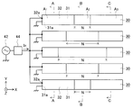
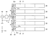
- the example shown in FIGS. 19 and 20 includes a plurality of antennas 30 and these are arranged in parallel to each other in the Y direction. That is, they are arranged side by side in the Y direction.
- the number of antennas 30 is five in the illustrated example, but is not limited to this.
- adopted the technique as described in FIG.19, FIG.20 etc. comprehensively is an example of FIG. 32 mentioned later, when this figure is referred, the whole is easy to understand.
- the lower conductor 31 is a flat conductor and corresponds to the conductor 31 shown in FIG. The same applies to other examples described later.
- high frequency power is supplied in parallel to the plurality of antennas 30 from a common high frequency power supply 42 via a matching circuit 44.
- the high frequency power supply 42 is connected to the end portion 32a (the end portion opposite to the connection portion 33 shown in FIG. 1) of the upper conductor 32 constituting each antenna 30 via the matching circuit 44.
- the end portion 31a of the lower conductor 31 (the end portion opposite to the connection portion 33) is grounded (direct grounding in this example). That is, the end portion 32a of each upper conductor 32 is used as a supply end for high-frequency power, and the end portion 31a of each lower conductor 31 is used as a termination point.
- the length N of the antenna A in the antenna longitudinal direction X of the region A 2 having a small conductor interval at the center of each antenna 30 is relatively increased in the antenna 30 at the center in the parallel arrangement direction Y of the plurality of antennas 30.
- the antennas 30 at both ends are relatively small.
- FIGS. 19 and 20 have the same effects as those described above for the examples shown in FIGS.
- a larger area means a larger area than when one antenna 30 is used.
- Plasma density distribution is as follows.
- FIG. 23 shows a schematic example of a two-dimensional plasma density distribution obtained when a plurality of known simple planar antennas long in the X direction are arranged in parallel in the Y direction.
- the two-dimensional plasma density distribution, film thickness distribution, and magnetic flux density distribution are shown in a simplified manner as concentric circles or circles for the sake of convenience. Is not limited to concentric circles or circles.
- the shape may be broken from a concentric circle or a circle, or it may be an ellipse or a rounded rectangle.
- the plasma density distribution in the antenna longitudinal direction X is the plasma density at the center. It becomes a mountain-shaped distribution with a smaller plasma density at both ends. The reason for this will be briefly explained.
- the plasma diffuses from the left and right sides in the X direction in the central portion, whereas the plasma diffuses only from one side at both ends.
- the plasma density distribution in the antenna parallel arrangement direction Y is also a peak in which the plasma density at both ends is smaller than the plasma density at the center. It becomes a type distribution. The reason for this will be briefly described.
- the plasma diffuses from the left and right sides in the Y direction in the central portion, whereas the plasma diffuses only from one side at both ends.
- the two-dimensional plasma density distribution obtained when a plurality of known simple planar antennas that are long in the X direction are arranged in parallel in the Y direction is as shown in FIG. It becomes a mountain-shaped distribution that rises near the center.
- the film thickness distribution is also a mountain-shaped distribution in which the vicinity of the central portion is raised like the plasma density distribution. become.
- the distance D in the vertical direction Z between the reciprocating conductors 31 and 32 of each antenna 30 is relatively small in the central portion in the antenna longitudinal direction X.
- the plasma is generated from each antenna 30 for the reason described above using Equations 3 and 4 as in the case of the example shown in FIGS. 50 electromagnetic energy supplied (see FIG. 1. hereinafter the same), it is possible to increase relatively near both ends than near the center of the antenna longitudinal direction X, i.e. a high-frequency current I R to each antenna 30 Since the magnetic flux density generated near the lower part of each antenna 30 by flowing can be made relatively larger near both ends than near the center in the antenna longitudinal direction X. It is possible to improve the uniformity of the plasma density distribution in the longitudinal direction X of the antenna 30.
- the length N in the antenna longitudinal direction X of the region A 2 having a small conductor interval D at the center of each antenna 30 is relatively increased in the antenna 30 at the center in the parallel arrangement direction Y of the plurality of antennas.
- the electromagnetic energy supplied from the plurality of antennas 30 to the plasma 50 is centered in the antenna parallel arrangement direction Y for the reason described above using Equations 3 and 4 by making the antenna 30 relatively small. It can be made relatively larger in the vicinity of both end portions than in the vicinity of the portion. That is, the magnetic flux density generated in the vicinity below the antenna group by passing a high frequency current I R in parallel to a plurality of antennas 30, relatively large near both end portions than near the center of the antenna parallel arrangement direction Y Can do.
- the length N of the region A 2 is small at both ends in the antenna parallel arrangement direction Y, so that the magnetic flux density is relative. to increase, in the central portion is from the magnetic flux density and the length N of the region a 2 is large becomes relatively small. As a result, the uniformity of the plasma density distribution in the antenna parallel arrangement direction Y can be improved.
- the uniformity of the plasma density distribution in the longitudinal direction X and the parallel arrangement direction Y of the antenna 30 can be improved, that is, the uniformity of the two-dimensional plasma density distribution can be improved.
- planar shape of the substrate 2 is illustrated as a quadrangle, but as described above, the planar shape of the substrate 2 is not limited to this, and may be a circle or the like.
- FIG. 24 shows a schematic example of a two-dimensional magnetic flux density distribution near the lower part of the antenna group obtained in the case of the examples shown in FIGS.
- the magnetic flux density distribution is a distribution in which the vicinity of the central portion is depressed as shown in FIG.
- plasma generation effects produced by passing a high frequency current I R also becomes recessed is near the center as well distributed as Figure 24 to the antenna group.
- the plasma density distribution shown in FIG. 23 can be corrected by the plasma generation operation having such a distribution, the uniformity of the plasma density distribution in two dimensions in the XY directions is improved as in the example shown in FIG. Can do.
- the degree of correction for example, adjusting the length N of the antenna longitudinal direction X of each interval D 1 ⁇ D 3 and / or the areas A 1 ⁇ A 3 in the respective regions A 1 ⁇ A 3 of each antenna 30 Can be adjusted.
- the uniformity of substrate processing in two dimensions can be improved, processing with good uniformity can be performed on the substrate 2 having a larger area.
- a film having a uniform film thickness distribution in the substrate plane can be formed on the substrate 2 having a larger area, for example, as shown in FIG. it can.
- the length N in the antenna longitudinal direction X of the region A 2 having a small conductor interval D in the central portion of each antenna 30 is relatively set in the central antenna 30 in the parallel arrangement direction Y of the plurality of antennas.
- FIG. 18 and its explanation can be obtained by increasing the size and relatively reducing the size of the antenna 30 at both ends without inserting an impedance element for adjusting the high-frequency current between each antenna 30 and the high-frequency power source 42.
- the uniformity of the plasma density distribution in the parallel arrangement direction Y of the plurality of antennas 30 can be improved without inserting an inductance, a capacitance, or the like as described above. Therefore, the circuit configuration can be simplified.
- the plurality of antennas 30 arranged in parallel in the Y direction may be as illustrated in FIGS. 21 and 22. Note that an example in which the techniques described in FIG. 21, FIG. 22 and the like are comprehensively adopted is an example of FIG. 33 to be described later.
- FIGS. 21 and 22 will be described mainly with respect to the differences from the examples shown in FIGS. 19 and 20.
- the region A 2 having a small conductor interval D at the center of each antenna 30 is described.
- the conductor spacing D of the corresponding portions of 30 is relatively small in the central antenna in the parallel arrangement direction Y of the plurality of antennas 30 and relatively large in the antennas at both ends. That is, the conductor spacing D 1 of the area A 1 of each antenna 30 (see FIG. 22 (A)), (see FIG.
- the plasma density distribution will be described.
- the distance D in the vertical direction Z between the reciprocating conductors 31 and 32 of each antenna 30 relatively small at the center in the antenna longitudinal direction X and relatively large at both ends. Since the electromagnetic energy supplied from each antenna 30 to the plasma 50 can be made relatively larger near both ends than near the center in the antenna longitudinal direction X, the plasma density distribution in the longitudinal direction X of each antenna 30 can be increased. Uniformity can be improved. This is the same as in the examples of FIGS.
- the conductor interval D of the portions corresponding to each antenna 30 is made relatively larger near the both ends than near the center in the antenna parallel arrangement direction Y for the reasons described using Equations 3 and 4 above. be able to. That is, the magnetic flux density generated in the vicinity below the antenna group by passing a high frequency current I R in parallel to a plurality of antennas 30, relatively large near both end portions than near the center of the antenna parallel arrangement direction Y Can do. To put it simply, the magnetic flux density is relatively large at both ends in the antenna parallel arrangement direction Y, and the magnetic flux density is relatively large. is there. As a result, the uniformity of the plasma density distribution in the antenna parallel arrangement direction Y can be improved.
- the uniformity of the plasma density distribution in the longitudinal direction X and the parallel arrangement direction Y of the antenna 30 can be improved, that is, the uniformity of the two-dimensional plasma density distribution can be improved.
- the magnetic flux density distribution in the vicinity of the lower part of the antenna group is a distribution in which the vicinity of the central portion is depressed as in the example shown in FIG.
- plasma generation effects produced by passing a high frequency current I R also becomes recessed is near the center as well distributed as Figure 24 to the antenna group.
- the plasma density distribution shown in FIG. 23 can be corrected by the plasma generation operation having such a distribution, the uniformity of the plasma density distribution in two dimensions in the XY directions is improved as in the example shown in FIG. Can do.
- the degree of correction for example, adjusting the length N of the antenna longitudinal direction X of each interval D 1 ⁇ D 3 and / or the areas A 1 ⁇ A 3 in the respective regions A 1 ⁇ A 3 of each antenna 30 Can be adjusted.
- the uniformity of substrate processing in two dimensions can be improved, processing with good uniformity can be performed on the substrate 2 having a larger area.
- a film having a uniform film thickness distribution in the substrate plane can be formed on the substrate 2 having a larger area, for example, as shown in FIG. it can.
- the technique as shown in FIGS. 19 and 20 and the technique as shown in FIGS. 20 and 21 may be used in combination.
- the example shown in FIG. 26 is arranged on one end side of the plurality of antennas 30 (on the side of the end portions 31a and 32a opposite to the connection portion 33 described above), and is close to each other and arranged in parallel.
- the flat plate conductor 84 and the second flat plate conductor 86 are further provided, and the plurality of antennas 30 are connected to the first and second flat plate conductors 84 and 86 in parallel with each other.
- the high-frequency power source 42 is connected to the plurality of antennas 30 by using one of the first and second plate conductors 84 and 86 as an outward path of the high-frequency current I R and using the other plate conductor as a return path of the high-frequency current I R. Supply high-frequency power in parallel.
- the end 32a of the upper conductor 32 of each antenna 30 is connected to the first flat conductor 84, and the end 31a of the lower conductor 31 of each antenna 30 is connected to the second flat conductor 86. Is connected.
- the high frequency power source 42 is connected to the first flat plate conductor 84 via the matching circuit 44, and the second flat plate conductor 86 is grounded (in this example, direct grounding).
- the flat conductor 86 may be grounded via a capacitor. The reason will be described later.
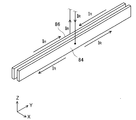
- Both flat plate conductors 84 and 86 are enlarged and shown in FIG. These are parallel plate conductors extending along the Y direction.
- the flat conductors 84 and 86 are electrically insulated by, for example, sandwiching a thin insulator between them or providing an insulating spacer.
- the mutual impedance between the first and second flat conductors 84 and 86 and the inductance of both flat conductors 84 and 86 are reduced.
- the high-frequency power loss in the first and second flat conductors 84 and 86 is reduced. Accordingly, it is possible to more efficiently supply the high frequency power from the common high frequency power supply 42 to the plurality of antennas 30 and to efficiently input the high frequency power by plasma generation, thereby further improving the plasma generation efficiency and hence the utilization efficiency of the high frequency power. be able to.
- the positions of feeding power to both the flat conductors 84 and 86 are the longitudinal direction (Y direction) of both flat conductors 84 and 86 as in the example shown in FIG. It is preferable to be near the central part. This is because the high frequency current I R can be supplied to each antenna 30 with a good balance.
- the high frequency power source 42 is connected to the end portion 32a of the upper conductor 32 constituting each antenna 30 via the matching circuit 44, and the lower conductor is formed.
- the end 31a of 31 is preferably grounded (directly grounded or grounded via a capacitor). The reason will be described below.
- the flat conductors 84 and 86 are not shown for the sake of simplicity, but there is no problem in the description of the electric circuit.
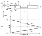
- the example shown in FIG. 28 corresponds to a simplified version of the antenna 30, the high-frequency power source 42, and the matching circuit 44 shown in FIGS.
- the high-frequency power source 42 is connected to the end 31 a opposite to the connection portion 33 of the lower conductor 31 via the matching circuit 44, and the end 32 a opposite to the connection portion 33 of the upper conductor 32 is connected.
- Grounded direct grounding in this example. That is, the end 31a of the lower conductor 31 is a supply end for high-frequency power, and the end 32a of the upper conductor 32 is a termination point.
- the antenna 30 (more specifically, the same below 33. conductors 31 and 32 and the connecting portion constituting it) has an impedance, it a potential difference is generated when high frequency current I R.
- the matching circuit 44 normally has an end portion on the side of the matching circuit 44 (that is, the high-frequency power source 42 side) (for example, in the example of FIG. 28), for example, because it has a series capacitor 64 as in the example shown in FIG. Then, the potential of the end portion 31a) is the highest.
- FIG. 28B shows a schematic example of the potential distribution of the antenna 30 in this case.
- the potential of the lower conductor 31 is higher than the potential of the upper conductor 32.
- the lower conductor 31 is located on the plasma 50 side, and the potential of the lower conductor 31 is reflected more strongly in the plasma potential than the potential of the upper conductor 32, so that the potential of the lower conductor 31 is as described above.
- the plasma potential also increases as the value increases.
- the plasma potential increases, as described above, the energy of charged particles incident on the substrate 2 from the plasma 50 also increases, and damage to the film formed on the substrate 2 also increases.
- the example shown in FIG. 28 still has room for improvement in this respect.
- a high-frequency power source 42 is connected to the end portion 32a of the upper conductor 32 via a matching circuit 44, and the end portion 31a of the lower conductor 31 is grounded (direct grounding in this example). That is, the end portion 32a of the upper conductor 32 is used as a supply end for high-frequency power, and the end portion 31a of the lower conductor 31 is used as a termination point.
- FIG. 29B shows a schematic example of the potential distribution of the antenna 30 in this case.
- the potential of the lower conductor 31 is lower than the potential of the upper conductor 32.
- the lower conductor 31 is located on the plasma 50 side, and the potential of the lower conductor 31 is reflected more strongly in the plasma potential than the potential of the upper conductor 32, so that the potential of the lower conductor 31 is as described above.
- the plasma potential also decreases as the temperature decreases. That is, in the example of FIG. 29, the plasma potential can be suppressed lower than in the example of FIG.
- the above-described effect by suppressing the plasma potential that is, the energy of charged particles incident on the substrate 2 from the plasma 50 can be suppressed low, and the plasma potential can be suppressed even when the antenna 30 is lengthened. Etc. can be further enhanced.
- end portion 32a of the upper conductor 32 and the end portion 31a of the lower conductor 31 are grounded, they may be grounded via a capacitor (series capacitor) instead of being directly grounded as in the above example.
- a capacitor series capacitor
- FIG. 26 employs the power feeding method shown in FIG. 29, so the above effect can be achieved.
- the upper conductor 32 and the lower conductor 31 constituting each antenna 30 are made different structures, and the position of the upper conductor 32 is changed in the vertical direction Z as indicated by an arrow J ( Position adjustment) may be possible.
- the method of feeding power to the antenna 30 is the same as the example shown in FIGS.
- the flat conductors 84 and 86 are not shown for the sake of simplicity, but the relationship with the flat conductors 84 and 86 will be described later with reference to FIGS. 32 and 33. .
- the end portions 31 b and 32 b on the same side of both the conductors 31 and 32 are electrically connected to each other by the connection portion 33 and further via the position adjustment portion 70 in this example.
- the position adjusting unit 70 is capable of adjusting the position of the upper conductor 32 in the vertical direction Z and electrically connecting the end 32b of the upper conductor 32 and the connecting portion 33 to each other.
- the position of the upper conductor 32 is fixed by a fixing member 72.
- FIG. 70 An example of a more specific structure around the position adjusting unit 70 is shown in FIG.
- the fixing member 72 includes a bolt 73 and a nut 74 in this example.
- the number of both is two in the illustrated example, but is not limited to this.
- connection portion 33 (in other words, the extension portion 31c; the same applies hereinafter) has a hole 76 through which the bolt 73 is passed.
- An extension portion 32c obtained by extending the end portion 32b of the upper conductor 32 is provided and is bent upward so as to be close to the connection portion 33 in a substantially parallel manner.
- the extension portion 32 c can move (slide) in the up-down direction Z while being close to the connection portion 33.
- the extension 32c has a long hole (a hole long in the vertical direction Z) 78 through which the bolts 73 are passed.
- the long hole 78 is more preferable because the position of the upper conductor 32 in the vertical direction Z can be adjusted continuously (steplessly), but a plurality of holes are provided in the vertical direction Z instead of the long hole 78. May be.
- the position of the upper conductor 32 in the vertical direction Z can be changed (adjusted) by loosening the fixing member 72 and moving the upper conductor 32 in the vertical direction Z.
- the position of the upper conductor 32 can be fixed.
- the end portion 32 b of the upper conductor 32 and the connection portion 33 can be electrically connected.
- the upper conductor 32 can be attached / detached by the above structure, that is, the upper conductor 32 can be attached / detached by removing the fixing member 72, the upper conductor 32 can be exchanged.
- the connecting portion 33 may be a flexible conductor that allows the upper conductor 32 to move in the vertical direction Z.
- the position in the vertical direction Z can be adjusted. However, it is easier to adjust the position of the upper conductor 32 if the position adjusting unit 70 is provided.
- the upper conductor 32 and the lower conductor 31 constituting the antenna 30 are different structures, and the position of the upper conductor 32 can be changed in the vertical direction Z.
- the distance D in the vertical direction Z between the reciprocating conductors 31 and 32 can be easily adjusted.
- the distance D can be adjusted after the device is assembled.
- the magnetic field distribution of the antenna 30 can be adjusted, and consequently the plasma density distribution can be adjusted, so that it becomes easier to cope with the uniform plasma density distribution.
- the upper conductor 32 is detachable, so that the upper conductor 32 can be replaced with one having the same structure or another structure.
- FIG. 32 shows an example around a plurality of antennas that comprehensively adopt the techniques described with reference to FIGS. 19 to 20, 26, 29, and 30.
- FIG. FIG. 33 shows an example around a plurality of antennas that comprehensively employ the techniques described with reference to FIGS. 21 to 22, 26, 29, and 30.
- the flat conductors 84 and 86 are shifted upward.
- the positions of the antennas 30 on the side opposite to the position adjusting unit 70 that is, the ends on the side where the flat conductors 84 and 86 are provided are positioned.
- a position adjustment unit 70a having a structure similar to that of the adjustment unit 70 is provided.
- Each position adjustment unit 70 a enables the position adjustment of the upper conductor 32 in the vertical direction Z and electrically connects the end 32 a of the upper conductor 32 to the flat conductor 84.
- each position adjustment portion 70a is provided with an extension portion 31d obtained by extending the end portion 31a of each lower conductor 31 and bent upward.
- An extension part 32d is provided by extending the end part 32a of each upper conductor 32 and is bent upward.
- Flat conductors 84 and 86 are inserted between the extension portions 31d and 32d as indicated by an arrow K. The two flat conductors 84 and 86 are fixed so as to be close to each other and electrically insulated, for example, by sandwiching an insulating plate therebetween.
- the flat conductor 86 is fixed and electrically connected to the extension 31d of the lower conductor 31 by a fixing member (not shown) (for example, the same bolt and nut as the fixing member 72; hereinafter the same).
- a fixing member for example, the same bolt and nut as the fixing member 72; hereinafter the same.
- the end 31 a of the lower conductor 31 is electrically connected to the flat conductor 86.
- the extension part 32d of each upper conductor 32 has a long hole (a hole long in the vertical direction Z) 78a similar to the long hole 78 shown in FIG. 31, and the position of the antenna 30 in the vertical direction Z can be adjusted.
- it is fixed to and electrically connected to the flat conductor 84 by a fixing member (not shown).
- the position in the vertical direction Z of the upper conductor 32 of each antenna 30 can be adjusted.
- the positions of the upper conductors 32 of all the antennas 30 can be aligned in the vertical direction Z, and as shown in FIG. The position of Z can also be shifted.
- the upper conductor 32 of each antenna 30 is detachable, it can also be replaced.
- FIG. 33 are combined with the functions and effects described above with reference to FIGS. 19 to 31.
- the upper conductor 32 is positioned in the atmosphere. In the example shown in FIG. 1 as well, as described above, the upper conductor 32 is positioned in the atmosphere.
- the upper conductor 32 is positioned in the atmosphere, even if the inside of the vacuum vessel 4 is in a vacuum state, the position of the upper conductor 32 is adjusted without returning the inside of the vacuum vessel 4 to the atmospheric pressure state, and the upper conductor 32 is separated. Since it is possible to change to a shape, etc., the plasma density distribution described above can be easily adjusted. The time required for adjustment can also be shortened.
- the cooling effect of the upper conductor 32 can be improved if the upper conductor 32 is positioned in the atmosphere. It is also possible to forcibly cool the upper conductor 32 by blowing air from the fan. Therefore, the cooling efficiency of the upper conductor 32 can be increased.
Landscapes
- Physics & Mathematics (AREA)
- Engineering & Computer Science (AREA)
- Plasma & Fusion (AREA)
- Electromagnetism (AREA)
- Spectroscopy & Molecular Physics (AREA)
- Chemical & Material Sciences (AREA)
- Analytical Chemistry (AREA)
- Plasma Technology (AREA)
- Chemical Vapour Deposition (AREA)
- Drying Of Semiconductors (AREA)
Abstract
この発明は、誘導結合型のプラズマ処理装置において、アンテナの実効インダクタンスを小さくしてプラズマ電位を低く抑え、かつ、より大面積でしかも2次元におけるプラズマ密度分布の均一性の良いプラズマの生成を可能にすることを主目的としている。 平面形状がまっすぐなアンテナ30を、上下方向Zに互いに接近して配置されていて高周波電流IR が互いに逆向きに流される往復導体31、32によって構成している。往復導体31、32間の上下方向Zの間隔Dを、アンテナ長手方向Xにおける中央部において小さくし、両端部において大きくしている。このようなアンテナ30を複数、並列配置している。各アンテナ中央部の間隔Dの小さい領域A2 の長さNを、並列配置方向Yの中央部で大きくし、両端部で小さくしている。
Description
この発明は、プラズマを用いて基板に、例えばプラズマCVD法による膜形成、エッチング、アッシング、スパッタリング等の処理を施すプラズマ処理装置に関し、より具体的には、アンテナに高周波電流を流すことによって発生する誘導電界によってプラズマを生成し、当該プラズマを用いて基板に処理を施す誘導結合型のプラズマ処理装置に関する。
本出願は、特許第4844697号(プラズマ処理装置)の更なる改良の発明に関するものである。
高周波を用いてプラズマを生成するプラズマ処理装置に属するものとして、容量結合型プラズマ(略称CCP)を生成する容量結合型のプラズマ処理装置と、誘導結合型プラズマ(略称ICP)を生成する誘導結合型のプラズマ処理装置とがある。
容量結合型のプラズマ処理装置は、簡単に言えば、2枚の平行電極間に高周波電圧を印加して、両電極間に発生する高周波電界を用いてプラズマを生成するものである。
この容量結合型のプラズマ処理装置においては、プラズマに高い電圧が印加されてプラズマ電位が高くなり、プラズマ中の荷電粒子(例えばイオン)が高いエネルギーで基板に入射衝突するので、基板上に形成する膜に与えるダメージが大きくなり、膜質が低下する等の課題がある。
一方、誘導結合型のプラズマ処理装置は、簡単に言えば、アンテナに高周波電流を流すことによって発生する誘導電界によってプラズマを生成するものであり、基本的に、容量結合型に比べてプラズマ電位を低くすることができる等の利点がある。
このような誘導結合型のプラズマ処理装置の一例として、特許文献1には、平板状のアンテナを真空容器の開口部に絶縁枠を介して取り付け、当該アンテナの一端と他端間に高周波電源から高周波電力を供給して高周波電流を流し、それによって発生する誘導電界によってプラズマを生成し、当該プラズマを用いて基板に処理を施すプラズマ処理装置が記載されている。
誘導結合型のプラズマ処理装置においても、大型の基板に対応する等のためにアンテナを長くすると、当該アンテナのインピーダンス(特にインダクタンス)が大きくなり、それによってアンテナの両端間に大きな電位差が発生する。
このアンテナの電位は、プラズマとの間の静電容量を介してプラズマ電位に反映されるので、アンテナの電位が高いとプラズマ電位も高くなる。その結果、プラズマ中の荷電粒子(例えばイオン)が高いエネルギーで基板に入射衝突するので、基板上に形成する膜に与えるダメージが大きくなり、膜質が低下する等の課題が生じる。
そこでこの発明は、誘導結合型の装置であって、アンテナの実効インダクタンスを小さくしてプラズマ電位を低く抑えることができ、しかも当該アンテナによってその長手方向におけるプラズマ密度分布を制御することができるプラズマ処理装置を提供することを主たる目的としている。更に、より大面積で、しかも2次元におけるプラズマ密度分布の均一性の良いプラズマの生成を可能にすること等を他の目的としている。
この発明に係るプラズマ処理装置の一つは、平面形状が実質的にまっすぐなアンテナに高周波電流を流すことによって真空容器内に誘導電界を発生させてプラズマを生成し、当該プラズマを用いて基板に処理を施す誘導結合型のプラズマ処理装置であって、前記アンテナを、前記基板の表面に立てた垂線を伸縮させる方向に互いに接近して配置されていて前記高周波電流が互いに逆向きに流される往復導体によって構成し、かつ前記往復導体間の前記垂線を伸縮させる方向の間隔を、前記アンテナの長手方向における中央部において相対的に小さくし、両端部において相対的に大きくしており、更に前記アンテナを複数備えていてこれらは互いに並列に配置されており、当該複数のアンテナに共通の高周波電源から高周波電力を並列に供給するように構成しており、かつ前記各アンテナの前記中央部の導体間隔の小さい領域のアンテナ長手方向における長さを、前記複数のアンテナの並列配置方向における中央部のアンテナにおいて相対的に大きくし、両端部のアンテナにおいて相対的に小さくしている、ことを特徴としている。
以下においては、表現を簡略化するために、基板の表面に立てた垂線を伸縮させる方向を上下方向と呼び、当該垂線に交差する方向を左右方向と呼ぶ。従って、上下方向は必ずしも垂直方向とは限らない。
このプラズマ処理装置においては、各アンテナについて言えば、アンテナを、上下方向に互いに接近して配置されていて高周波電流が互いに逆向きに流される往復導体によって構成しているので、往復導体間の相互インダクタンスのぶん、アンテナの実効インダクタンスが小さくなる。従って、アンテナの電位を低く抑えて、プラズマ電位を低く抑えることができる。
しかも、往復導体間の上下方向の間隔をアンテナの長手方向において変化させることによって、往復導体間の相互インダクタンスをアンテナの長手方向において変化させることができるので、アンテナからプラズマに供給する電磁エネルギーを、アンテナの長手方向において変化させることができる。従って、このアンテナによって、その長手方向におけるプラズマ密度分布を制御することができる。
また、互いに並列に配置され、かつ並列に高周波電力が供給される複数のアンテナを備えているので、より大面積のプラズマを生成することができる。
更に、各アンテナの往復導体間の上下方向の間隔を、アンテナ長手方向における中央部において相対的に小さくし、両端部において相対的に大きくすることによって、各アンテナからプラズマに供給する電磁エネルギーを、アンテナ長手方向における中央部付近よりも両端部付近において相対的に大きくすることができるので、各アンテナの長手方向におけるプラズマ密度分布の均一性を良くすることができる。
かつ各アンテナの中央部の導体間隔の小さい領域のアンテナ長手方向における長さを、複数のアンテナの並列配置方向における中央部のアンテナにおいて相対的に大きくし、両端部のアンテナにおいて相対的に小さくすることによって、複数のアンテナからプラズマに供給する電磁エネルギーを、アンテナ並列配置方向における中央部付近よりも両端部付近において相対的に大きくすることができるので、複数のアンテナの並列配置方向におけるプラズマ密度分布の均一性を良くすることができる。
上記両作用によって、アンテナの長手方向および並列配置方向におけるプラズマ密度分布の均一性を、即ち2次元におけるプラズマ密度分布の均一性を良くすることができる。
各アンテナの中央部の導体間隔の小さい領域のアンテナ長手方向における長さに上記のように差を付ける代りに、またはそれと併用して、各アンテナの互いに対応する部分の導体間隔を、複数のアンテナの並列配置方向における中央部のアンテナにおいて相対的に小さくし、両端部のアンテナにおいて相対的に大きくしても良い。
高周波電源から、互いに平行に近接配置された第1および第2の平板導体の内の一方の平板導体を高周波電流の往路とし、他方の平板導体を高周波電流の復路として、前記複数のアンテナに高周波電力を並列に供給するようにしても良い。
請求項1に記載の発明によれば次の効果を奏する。
(a)各アンテナについて言えば、アンテナを、上下方向に互いに接近して配置されていて高周波電流が互いに逆向きに流される往復導体によって構成しているので、往復導体間の相互インダクタンスのぶん、アンテナの実効インダクタンスが小さくなる。従って、アンテナの電位を低く抑えて、プラズマ電位を低く抑えることができる。その結果、プラズマから基板に入射する荷電粒子のエネルギーを小さく抑えることができる。それによって例えば、基板上に形成する膜に与えるダメージを小さく抑えて、膜質向上を図ることができる。また、アンテナを長くする場合でも、上記理由によって、アンテナの電位を低く抑えてプラズマ電位を低く抑えることができるので、アンテナを長くして基板の大型化に対応することが容易になる。
(b)各アンテナについて言えば、往復導体間の上下方向の間隔をアンテナの長手方向において変化させることによって、往復導体間の相互インダクタンスをアンテナの長手方向において変化させることができるので、アンテナからプラズマに供給する電磁エネルギーを、アンテナの長手方向において変化させることができる。従って、このアンテナによって、その長手方向におけるプラズマ密度分布を制御することができる。その結果、アンテナの長手方向における基板の処理状態を制御することができる。例えば、アンテナの長手方向における膜厚分布を制御することができる。
(c)各アンテナについて言えば、アンテナを、上下方向に互いに接近して配置されていて高周波電流が互いに逆向きに流される往復導体によって構成し、かつ当該往復導体間の上下方向の間隔をアンテナの長手方向において変化させているので、左右方向に互いに接近して配置された往復導体間の左右方向の間隔を変化させる場合に比べて、往復導体間の間隔変化によるアンテナ下方近傍の磁束密度の制御性が良い。従って、往復導体間の間隔を変化させることによる、アンテナからプラズマに供給する電磁エネルギーの制御性、ひいてはプラズマ密度分布の制御性が良い。
(d)互いに並列に配置され、かつ並列に高周波電力が供給される複数のアンテナを備えているので、より大面積のプラズマを生成することができる。
(e)各アンテナの往復導体間の上下方向の間隔を、アンテナ長手方向における中央部において相対的に小さくし、両端部において相対的に大きくすることによって、各アンテナからプラズマに供給する電磁エネルギーを、アンテナ長手方向における中央部付近よりも両端部付近において相対的に大きくすることができるので、各アンテナの長手方向におけるプラズマ密度分布の均一性を良くすることができる。かつ各アンテナの中央部の導体間隔の小さい領域のアンテナ長手方向における長さを、複数のアンテナの並列配置方向における中央部のアンテナにおいて相対的に大きくし、両端部のアンテナにおいて相対的に小さくすることによって、複数のアンテナからプラズマに供給する電磁エネルギーを、アンテナ並列配置方向における中央部付近よりも両端部付近において相対的に大きくすることができるので、複数のアンテナの並列配置方向におけるプラズマ密度分布の均一性を良くすることができる。上記両作用によって、アンテナの長手方向および並列配置方向におけるプラズマ密度分布の均一性を、即ち2次元におけるプラズマ密度分布の均一性を良くすることができる。その結果、2次元における基板処理の均一性を高めることができるので、より大面積の基板に対して均一性の良い処理を施すことができる。例えば、より大面積の基板に対して、基板面内における膜厚分布の均一性の良い膜を形成することができる。
(f)各アンテナの中央部の導体間隔の小さい領域のアンテナ長手方向における長さを、複数のアンテナの並列配置方向における中央部のアンテナにおいて相対的に大きくし、両端部のアンテナにおいて相対的に小さくすることによって、各アンテナと高周波電源との間に高周波電流調整用のインピーダンス素子を挿入しなくても、複数のアンテナの並列配置方向におけるプラズマ密度分布の均一性を良くすることができる。従って、回路構成を簡素化することができる。かつ、上記インピーダンス素子における電力損失がないので、各アンテナに高周波電源から高周波電力を効率良く供給して、高周波電力をプラズマ生成に効率良く投入することができる。その結果、プラズマ生成効率ひいては高周波電力の利用効率を高めることができる。
請求項2に記載の発明によれば、請求項1記載の発明の上記(a)~(d)の効果と同様の効果に加えて次の効果を奏する。
(g)各アンテナの往復導体間の上下方向の間隔を、アンテナ長手方向における中央部において相対的に小さくし、両端部において相対的に大きくすることによって、各アンテナからプラズマに供給する電磁エネルギーを、アンテナ長手方向における中央部付近よりも両端部付近において相対的に大きくすることができるので、各アンテナの長手方向におけるプラズマ密度分布の均一性を良くすることができる。かつ各アンテナの互いに対応する部分の導体間隔を、複数のアンテナの並列配置方向における中央部のアンテナにおいて相対的に小さくし、両端部のアンテナにおいて相対的に大きくすることによって、複数のアンテナからプラズマに供給する電磁エネルギーを、アンテナ並列配置方向における中央部付近よりも両端部付近において相対的に大きくすることができるので、複数のアンテナの並列配置方向におけるプラズマ密度分布の均一性を良くすることができる。上記両作用によって、アンテナの長手方向および並列配置方向におけるプラズマ密度分布の均一性を、即ち2次元におけるプラズマ密度分布の均一性を良くすることができる。その結果、2次元における基板処理の均一性を高めることができるので、より大面積の基板に対して均一性の良い処理を施すことができる。例えば、より大面積の基板に対して、基板面内における膜厚分布の均一性の良い膜を形成することができる。
(h)各アンテナの互いに対応する部分の導体間隔を、複数のアンテナの並列配置方向における中央部のアンテナにおいて相対的に小さくし、両端部のアンテナにおいて相対的に大きくすることによって、各アンテナと高周波電源との間に高周波電流調整用のインピーダンス素子を挿入しなくても、複数のアンテナの並列配置方向におけるプラズマ密度分布の均一性を良くすることができる。従って、回路構成を簡素化することができる。かつ、上記インピーダンス素子における電力損失がないので、各アンテナに高周波電源から高周波電力を効率良く供給して、高周波電力をプラズマ生成に効率良く投入することができる。その結果、プラズマ生成効率ひいては高周波電力の利用効率を高めることができる。
請求項3に記載の発明によれば次の更なる効果を奏する。即ち、高周波電源から、互いに平行に近接配置された第1および第2の平板導体の内の一方の平板導体を高周波電流の往路とし、他方の平板導体を高周波電流の復路として、前記複数のアンテナに高周波電力を並列に供給するようにしているので、第1および第2の平板導体に流れる高周波電流は、互いに接近した状態で逆向きに流れる。その結果、第1および第2の平板導体間の相互インピーダンスのぶん、両平板導体のインダクタンスが小さくなるので、第1および第2の平板導体における高周波電力損失が小さくなる。従って、複数のアンテナに共通の高周波電源から高周波電力をより効率良く供給して、高周波電力をプラズマ生成により効率良く投入することができるので、プラズマ生成効率ひいては高周波電力の利用効率をより高めることができる。
請求項4に記載の発明によれば次の更なる効果を奏する。即ち、第1および第2の平板導体をそれぞれ介して、各アンテナを構成する上側導体の他方端部が整合回路を介して高周波電源に接続され、下側導体の他方端部が直接またはコンデンサを介して接地された構成になるので、下側導体の電位の方が上側導体の電位よりも低くなる。この下側導体はプラズマ側に位置していて、当該下側導体の電位の方が上側導体の電位よりもプラズマ電位に強く反映されるので、当該下側導体の電位が上記のように低くなることによって、プラズマ電位をより低く抑えることができる。その結果、プラズマ電位を低く抑えることによる請求項1、2の上記(a)の効果(即ち、プラズマから基板に入射する荷電粒子のエネルギーを低く抑えることができる、アンテナを長くする場合でもプラズマ電位を低く抑えることができる、等の効果)をより高めることができる。
この発明に係るプラズマ処理装置の一実施形態を図1に示し、そのアンテナ30を抜き出して図2に示す。アンテナ30等の向きを表すために、一点で互いに直交するX方向、Y方向およびZ方向を図中に記載している。Z方向は基板2の表面に立てた垂線3を伸縮させる方向であり、Y方向は当該垂線3に交差する(例えば直交する)方向であり、これらは、前述したように表現を簡略化するために、それぞれ、上下方向Z、左右方向Yと呼ぶことにする。X方向は、垂線3に交差する(例えば直交する)方向であり、かつアンテナ30の長手方向である。例えば、X方向およびY方向は水平方向であるが、これに限られるものではない。以上のことは、他の図においても同様である。
この装置は、平面形状が実質的にまっすぐなアンテナ30に高周波電源42から高周波電流IR を流すことによって真空容器4内に誘導電界を発生させて当該誘導電界によってプラズマ50を生成し、このプラズマ50を用いて基板2に処理を施す誘導結合型のプラズマ処理装置である。
「実質的にまっすぐ」というのは、文字どおりまっすぐな状態だけでなく、まっすぐに近い状態(ほぼまっすぐな状態)をも含む意味である。
基板2は、例えば、液晶ディスプレイや有機ELディスプレイ等のフラットパネルディスプレイ(FPD)用の基板、フレキシブルディスプレイ用のフレキシブル基板、太陽電池等の半導体デバイス用の基板等であるが、これに限られるものではない。
基板2の平面形状は、例えば円形、四角形等であり、特定の形状に限定されない。
基板2に施す処理は、例えば、プラズマCVD法による膜形成、エッチング、アッシング、スパッタリング等である。
このプラズマ処理装置は、プラズマCVD法によって膜形成を行う場合はプラズマCVD装置、エッチングを行う場合はプラズマエッチング装置、アッシングを行う場合はプラズマアッシング装置、スパッタリングを行う場合はプラズマスパッタリング装置とも呼ばれる。
このプラズマ処理装置は、例えば金属製の真空容器4を備えており、その内部は真空排気装置8によって真空排気される。
真空容器4内には、ガス導入管22を通してガス24が導入される。ガス24は、基板2に施す処理内容に応じたものにすれば良い。例えば、プラズマCVD法によって基板2に膜形成を行う場合は、ガス24は、原料ガスまたはそれを希釈ガス(例えばH2 )で希釈したガスである。より具体例を挙げると、原料ガスがSiH4 の場合はSi 膜を、SiH4 +NH3 の場合はSiN膜を、SiH4 +O2 の場合はSiO2 膜を、それぞれ基板2の表面に形成することができる。
真空容器4内には、基板2を保持するホルダ10が設けられている。この例では、ホルダ10は軸16に支持されている。軸16が真空容器4を貫通する部分には、電気絶縁機能および真空シール機能を有する軸受部18が設けられている。この例のように、ホルダ10にバイアス電源20から軸16を経由して負のバイアス電圧を印加するようにしても良い。バイアス電圧は負のパルス状電圧でも良い。このようなバイアス電圧によって、例えば、プラズマ50中の正イオンが基板2に入射するときのエネルギーを制御して、基板2の表面に形成される膜の結晶化度を制御することができる。
真空容器4の天井面6の開口部7に、絶縁枠38を介在させて、アンテナ30が設けられている。これらの要素の間には、真空シール用のパッキン40がそれぞれ設けられている。このアンテナ30は、上下方向Zに互いに接近して配置されている往復導体31、32によって構成されている。アンテナ30(より具体的にはそれを構成している往復導体31、32)は、この例では、その平面形状が面状をしている。より具体的には、当該平面形状はこの実施形態では長方形であるが、これに限られるものではない。このアンテナ30については、後で詳述する。
アンテナ30の材質は、例えば、銅(より具体的には無酸素銅)、アルミニウム等であるが、これに限られるものではない。
アンテナ30には、より具体的にはその往復導体31、32には、高周波電源42から整合回路44を経由して、高周波電力が供給され、それによってアンテナ30に高周波電流IR が流される。即ち、アンテナ30を構成する往復導体31、32には、互いに逆向きの高周波電流(往復電流)IR が流される(高周波だから、この高周波電流IR の向きは時間によって反転する。以下同様)。この高周波電流IR によって、アンテナ30の周囲に高周波磁界が発生し、それによって高周波電流IR と逆方向に誘導電界が発生する。この誘導電界によって、真空容器4内において、電子が加速されてアンテナ30の近傍のガス24を電離させてアンテナ30の近傍にプラズマ50が発生する。このプラズマ50は基板2の近傍まで拡散し、このプラズマ50によって基板2に前述した処理を施すことができる。
高周波電源42は出力端42aおよび接地端42bを有しており、出力端42aは整合回路44を介して導体31の一端部に接続されている。接地端42bは接地されている。導体32の一端部も接地されている。
高周波電源42から出力する高周波電力の周波数は、例えば、一般的な13.56MHzであるが、これに限られるものではない。
整合回路44は、ラインに直列のコンデンサ64および並列のコンデンサ65を有している。両コンデンサ64、65はこの例では容量可変である。
上記アンテナ30について詳述する。図5に示すような、互いに接近している平行な往復導体61、62の総合インピーダンスZT は、差動接続として電気理論の書籍等にも記載されているように、次式で表される。ここで、R1 、L1 は、それぞれ、一方の導体61の抵抗、自己インダクタンス、R2 、L2 は、それぞれ、他方の導体62の抵抗、自己インダクタンス、Mは両導体61、62間の相互インダクタンスである。
[数1]
ZT =(R1 +R2 )+j(L1 +L2 -2M)
ZT =(R1 +R2 )+j(L1 +L2 -2M)
ここで、説明を簡略化するために、R1 =R2 =R、L1 =L2 =Lとすると、総合インピーダンスZT は数2で表され、その内のインダクタンスLT は数3で表される。このインダクタンスLT のように、自己インダクタンスと相互インダクタンスとを合成したものを、この明細書では実効インダクタンスと呼ぶことにする。
[数2]
ZT =2R+j2(L-M)
ZT =2R+j2(L-M)
[数3]
LT =2(L-M)
LT =2(L-M)
上記式からも分るように、往復導体61、62間の相互インダクタンスMが大きくなると、総合インピーダンスZT および実効インダクタンスLT は小さくなる。この往復導体61、62に高周波電源42から高周波電流IR を流すことによって発生する電磁エネルギーGは次式で表されるので、相互インダクタンスMが大きくなると、この電磁エネルギーGは小さくなり、外部に作用する磁気的な効果が減少する。プラズマ生成の場合は、プラズマへ供給できる電磁エネルギーが減少し、プラズマ密度が下がる。逆の場合は逆になる。
[数4]
G=(1/2)LTIR 2
=(L-M)IR 2
G=(1/2)LTIR 2
=(L-M)IR 2
往復導体61、62の長手方向において相互インダクタンスMが一様でない場合、即ち相互インダクタンスMを変化させている(換言すれば、変化を付けている)場合は、各領域について見れば、当該領域の相互インダクタンスMに応じて、上記実効インダクタンスおよび電磁エネルギーが決まる。
この発明を構成しているアンテナ30は、上記原理を応用したものである。例えば、図6に示す例のように、アンテナ30を、上下方向Zに互いに接近して配置されている往復導体31、32によって構成し、かつ往復導体31、32間の上下方向Zの間隔Dを、アンテナ30の長手方向Xにおいて2段階に変化させている場合、小さい間隔D2 の領域A2 の相互インダクタンスM2 よりも、大きい間隔D1 の領域A1 の相互インダクタンスM1 の方が小さくなる(即ちM1 <M2 )。従って、上記数3を参照すれば分るように、領域A2 よりも領域A1 の実効インダクタンスが大きくなり、上記数4を参照した説明からも分るように、アンテナ30(より具体的にはその導体31)から距離H1 だけ離れた空間の磁束密度は、領域A2 における磁束密度B2 よりも、領域A1 における磁束密度B1 の方が大きくなる(即ちB1 >B2 )。従って、領域A2 のプラズマ密度よりも、領域A1 のプラズマ密度を大きくすることができる。
なお、この図6や後述する他の例では、説明を簡略化するために整合回路44を省略しているが、通常は、図1に示す例と同様に、高周波電源42とアンテナ30との間には整合回路44が設けられる。
上下方向Zに配置された板状の往復導体31、32間の上下方向Zの間隔Dを変化させて、アンテナ30の中央下方近傍での磁束密度の変化をシミュレーションした結果を説明する。このシミュレーションに用いたモデルを図7に示す。両導体31、32の厚さTを3mm、左右方向Yの幅Wを70mmとし、X方向の長さを十分に長いものとして、一定の(ピーク値が100Aの)高周波電流IR を流したときの、導体31の左右方向Yにおける中央下方に距離H1 (5mmで固定)離れた点Pにおける磁束密度Bを、間隔Dを変化させて測定した。その結果を表1に示す。

表1中の磁束密度B0 は、導体32がなくて導体31だけの公知の平面アンテナの場合の点Pにおける磁束密度である。その場合の磁束密度B0 と、往復導体31、32の場合の磁束密度との比B/B0 およびその2乗比(B/B0 )2 を表1中に示す。2乗比(B/B0 )2 に着目しているのは、プラズマに対する電磁エネルギー供給は、渦電流損のように、近似的には磁束密度Bの2乗に比例するからである。この表から分るように、間隔Dを変化させることによって、磁束密度Bおよび2乗比(B/B0 )2 を大きく変化させることができる。例えば、間隔Dが1mmのときと50mmのときとでは、2乗比(B/B0 )2 に約60倍の差を付けることができる。
図8は、上下方向Zに互いに接近して配置されている往復導体31、32間の上下方向Zの間隔Dを、アンテナ30の長手方向Xにおける中央部の領域A2 の間隔D2 よりも両端部の領域A1 、A3 の間隔D1 、D3 (この例ではD1 =D3 )を段階的(階段状)に大きくした例である。換言すれば、往復導体31、32間の上下方向Zの間隔Dを、アンテナ30の長手方向Xにおける中央部の領域A2 において相対的に小さくし(その間隔はD2 )、両端部の領域A1 、A3 において相対的に大きくし(その間隔はD1 、D3 )、かつこの間隔D1 、D3 (この例ではD1 =D3 )を段階的(階段状)に大きくしている例である。この場合は、各領域A1 ~A3 の相互インダクタンスM1 ~M3 はM1 =M3 <M2 となり、領域A2 よりも領域A1 、A3 の実効インダクタンスが大きくなる。磁束密度B1 ~B3 はB1 =B3 >B2 となる。その結果、アンテナ30からプラズマに供給する電磁エネルギーを、中央部の領域A2 よりも両端部の領域A1 、A3 において相対的に大きくすることができる。
図1、図2に示すアンテナ30は、図8に示すアンテナ30に相当し、それをより具体化した例である。この図1、図2に示すアンテナ30について詳述すると、アンテナ30は、上下方向Zに間隔Dをあけて互いに接近して配置されている往復導体31、32を有している。両導体31、32は板状であり、その平面形状は前述したように長方形である。下側(プラズマ50側)の導体31の下面は真空容器4内の真空雰囲気中に位置しており、上側の導体32は大気中に位置している。両導体31、32の一端部は電気的に開いていて、そこにこの例では絶縁物36が設けられている。他端部は接続部33で互いに電気的に接続されている。両導体31、32の一端部間に、高周波電源42から整合回路44を経由して高周波電力が供給される。
両導体31、32は、この例では板状(具体的には、導体31は平板状、導体32は折り曲げられた板状)である。この場合、例えば、図1、図2(C)に示す例のように下側の導体31の厚さを大きくしても良いし、図3に示す例のように両導体31、32の厚さを互いに同程度にしても良い。
上側の導体32は、階段状に折り曲げられており、これによって、アンテナ30の長手方向Xにおける中央部の領域の間隔D2 よりも両端部の領域の間隔D1 、D3 (この例ではD1 =D3 )を段階的に大きくしている。このようにして、上述した説明からも分るように、アンテナ30の長手方向Xにおいて、中央部よりも両端部の相互インダクタンスMを段階的に小さくしている。即ち、この例ではM1 =M3 <M2 にしている。これによって、図8の場合と同様に、アンテナ30からプラズマ50に供給する電磁エネルギーを、アンテナ30の長手方向Xにおける中央部よりも両端部において相対的に大きくすることができる。
アンテナ30の上記間隔Dおよび相互インダクタンスMは、アンテナ30の長手方向Xにおいて、図1、図8等に示す例のように段階的に変化させても良いし、連続的に変化させても良い。後述する他の例においても同様である。上記間隔D等を段階的に変化させても、プラズマには拡散作用があるので、プラズマ密度を滑らかに変化させることができる。例えば、図1、図2に示す上側の導体32を、中央部が窪んだなだらかな谷状にして、アンテナ30の上記間隔Dおよび相互インダクタンスMを、アンテナ30の長手方向Xにおいて連続的に変化させても良い。
図1、図2、図8に示すアンテナ30の代わりに、図6に示した構造のアンテナ30を設けても良い。更には、図9等に示す他の構造のアンテナ30を設けても良い。
図9に示す例は、図1、図8に示す例を変形したものである。即ち、図1、図8に示す例のようにアンテナ30の端部から高周波電力を供給(端部給電)する代わりに、図9に示す例のようにアンテナ30の中央部から高周波電力を供給(中央給電)するようにしても良い。これと同様に、他の例のアンテナ30においても、中央給電にしても良い。
アンテナ30を構成する往復導体31、32は、例えば、前述した例のように板状でも良いし、図10に示す例のように棒状でも良いし、板状と棒状とを組み合わせたもの等でも良い。例えば、図11に示す例のように、下側の導体31が板状、上側の導体32が棒状でも良い。その場合、図12に示す例のように、上側の棒状の導体32を、互いに電気的に並列な複数本(図12では2本)にしても良い。これらの場合も、往復導体31、32は、長手方向Xの端部において接続部(図1中の接続部33参照)で互いに電気的に接続されている。
各導体31、32の断面形状は、図示例のものに限られるものではなく、円形、楕円形、四角形等が採り得る。また、各導体31、32を中空にして、そこに冷却水等の冷媒を流して、各導体31、32を強制的に冷却する構造を採用しても良い。
この発明に係るプラズマ処理装置においては、アンテナ30を、上下方向Zに互いに接近して配置されていて高周波電流IR が互いに逆向きに流される往復導体31、32によって構成しているので、上記数3を参照すれば分るように、往復導体31、32間の相互インダクタンスのぶん、アンテナ30の実効インダクタンスが小さくなる。高周波領域においては、アンテナ30のインピーダンスは殆どがインダクタンスであるので、実効インダクタンスが小さくなることによって、アンテナ30に発生する電位差を小さく抑えて、アンテナ30の電位を低く抑え、プラズマ50の電位を低く抑えることができる。
その結果、プラズマ50から基板2に入射する荷電粒子(例えばイオン)のエネルギーを小さく抑えることができる。それによって例えば、プラズマ50によって基板2上に膜を形成する場合、当該膜に与えるダメージを小さく抑えて、膜質向上を図ることができる。また、アンテナ30を長くする場合でも、上記理由によって、アンテナ30の電位を低く抑えてプラズマ電位を低く抑えることができるので、アンテナ30を長くして基板2の大型化に対応することが容易になる。
しかも、往復導体31、32間の上下方向Zの間隔Dをアンテナの長手方向Xにおいて変化させることによって、往復導体31、32間の相互インダクタンスMを、アンテナ30の長手方向Xにおいて変化させることができるので、アンテナ30からプラズマ50に供給する電磁エネルギーを、アンテナ30の長手方向Xにおいて変化させることができる。従って、このアンテナ30によって、その長手方向Xにおけるプラズマ密度分布を制御することができる。その結果、アンテナ30の長手方向Xにおける基板の処理状態を制御することができる。例えば、プラズマ50によって基板2上に膜を形成する場合、アンテナ30の長手方向Xにおける膜厚分布を制御することができる。
更に、アンテナ30を、上下方向Zに互いに接近して配置されていて高周波電流IR が互いに逆向きに流される往復導体31、32によって構成し、かつ当該往復導体31、32間の上下方向Zの間隔Dをアンテナ30の長手方向Xにおいて変化させているので、左右方向に互いに接近して配置された往復導体間の左右方向Yの間隔を変化させる場合に比べて、往復導体31、32間の間隔Dの変化によるアンテナ30の下方近傍の磁束密度の制御性が良い。従って、往復導体31、32間の間隔Dを変化させることによる、アンテナ30からプラズマ50に供給する電磁エネルギーの制御性、ひいてはプラズマ密度分布の制御性が良い。これを、シミュレーション結果に基づいて以下に説明する。
シミュレーションでは、アンテナ30を構成する往復導体31、32の間隔Dを変化させたときの、アンテナ30の左右方向Yにおける中央下方の点P(図7、図13~図15参照)での磁束密度Bの変化を計算した。
まず、この発明の一実施形態を成すものとして、先に図7に示したように、アンテナ30を構成する板状の往復導体31、32が上下方向Zに互いに接近して配置されている場合で、その往復導体31、32間の上下方向Zの間隔Dを変化させたときの上記点Pにおける磁束密度Bの変化を図16中に実施例として示す。このときの計算条件は、先に図7の説明箇所で説明したものと同じであり、この実施例は表1中の磁束密度Bと同じである。
また、上記に対する比較例として、図13に示すように、アンテナ30を構成する板状の往復導体31、32が左右方向Yに互いに接近して配置されている場合で、その往復導体31、32間の左右方向Yの間隔Dを変化させたときの上記点Pにおける磁束密度Bの変化を図16中に比較例として示す。このときの計算条件は、両導体31、32の厚さTを70mm、左右方向Yの幅Wを3mmとし、その他の距離H1 、高周波電流IR の大きさ等は図7の場合と同じにした。
図16から分るように、間隔Dを変化させたとき、比較例の場合は、磁束密度Bの変化がすぐに飽和してしまうのに対して、実施例の場合は、磁束密度Bがなだらかに比例に近い状態で変化しており、その変化幅も大きい。従って、比較例に比べて、実施例の方が磁束密度Bの制御性が良い。即ち、間隔Dを変化させることによって、磁束密度Bを制御し、それによってアンテナ30からプラズマに供給する電磁エネルギーを制御し、ひいてはプラズマ密度分布を制御する、という制御を行いやすい。
次に、この発明の一実施形態を成すものとして、図14に示すように、アンテナ30を構成する棒状の往復導体31、32が上下方向Zに互いに接近して配置されている場合で、その往復導体31、32間の上下方向Zの間隔Dを変化させたときの上記点Pにおける磁束密度Bの変化を図17中に実施例として示す。このときの計算条件は、両導体31、32の直径dを6mmとし、その他の距離H1 、高周波電流IR の大きさ等は図7の場合と同じにした。
また、上記に対する比較例として、図15に示すように、アンテナ30を構成する棒状の往復導体31、32が左右方向Yに互いに接近して配置されている場合で、その往復導体31、32間の左右方向Yの間隔Dを変化させたときの上記点Pにおける磁束密度Bの変化を図17中に比較例として示す。このときの計算条件は、両導体31、32の配置を上記のように変更した以外は、図14の場合と同じにした。
図17から分るように、間隔Dを変化させたとき、比較例の場合は、磁束密度Bが一旦上がった後に下がるという複雑な変化をしているのに対して、実施例の場合は、磁束密度Bがなだらかに比例に近い状態で変化している。従って、この場合も、比較例に比べて、実施例の方が磁束密度Bの制御性が良い。即ち、間隔Dを変化させることによって、磁束密度Bを制御し、それによってアンテナ30からプラズマに供給する電磁エネルギーを制御し、ひいてはプラズマ密度分布を制御する、という制御を行いやすい。
ところで、通常は、即ち公知の単純な平面アンテナを用いた場合は、その長手方向Xにおけるプラズマ密度分布は、例えば図4に示すように、中央部のプラズマ密度よりも両端部のプラズマ密度が小さい山型の分布になる。その理由を簡単に説明すると、中央部には左右両側からプラズマが拡散して来るのに対して、両端部は片側からしかプラズマが拡散して来ないからである。
これに対して、図1、図2、図8等に示した例のように、往復導体31、32間の上下方向Zの間隔Dを、アンテナ30の長手方向Xにおける中央部の間隔よりも両端部の間隔を大きくすることによって、換言すれば往復導体31、32間の上下方向Zの間隔Dを、アンテナ30の長手方向Xにおける中央部において相対的に小さくし、両端部において相対的に大きくすることによって、アンテナ30の長手方向Xにおいて、中央部よりも両端部の相互インダクタンスを小さくすることができるので、前述したように、アンテナ30の中央部よりも両端部の実効インダクタンスが相対的に大きくなる。その結果、アンテナ30からプラズマ50に供給する電磁エネルギーを、山型とは反対に、アンテナ30の長手方向Xにおける中央部付近よりも両端部付近において相対的に大きくして、中央部付近よりも両端部付近においてより強力にプラズマ50を生成することができるので、上記山型のプラズマ密度分布を補正して、アンテナ30の長手方向Xにおけるプラズマ密度分布の均一性を高めることができる。その結果、アンテナ30の長手方向における基板処理の均一性を高めることができる。例えば、プラズマ50によって基板2上に膜を形成する場合、アンテナ30の長手方向Xにおける膜厚分布の均一性を高めることができる。
なお、図1に示す実施形態のように、アンテナ30の真空容器4内側の面をプラズマ50から遮蔽する遮蔽板46を備えていても良い。遮蔽板46は絶縁物から成る。遮蔽板46は、真空容器4の天井面6の開口部7の入口部付近に直接取り付けても良いし、この実施形態のように枠状の支持板48を用いて取り付けても良い。図1に示す例以外のアンテナ30を用いる場合も、このような遮蔽板46を備えていても良い。
遮蔽板46の材質は、例えば、石英、アルミナ、炭化ケイ素、シリコン等である。水素系プラズマで還元されて遮蔽板46から酸素が放出されると困る場合は、シリコン、炭化ケイ素等の非酸化物系の材質を用いれば良い。例えばシリコン板を用いるのが簡単で良い。
遮蔽板46を設けておくと、アンテナ30等の表面がプラズマ50中の荷電粒子(主としてイオン)によってスパッタされてプラズマ50および基板2に対して金属汚染(メタルコンタミネーション)が生じること等の不都合発生を防止することができる。
遮蔽板46を設けていても、遮蔽板は絶縁物から成りアンテナ30の電位がプラズマ50に及ぶことを防止することはできないので、前述したようにアンテナ30の実効インダクタンスを小さくして、アンテナ30の電位を低く抑えることは有効である。
図18に示す例のように、前記構成のアンテナ30を、複数、互いにY方向に並列に配置し、各アンテナ30に、共通の高周波電源42から高周波電力を並列に供給するようにしても良い。更に図示例のように、各アンテナ30にそれぞれ直列に接続された可変インピーダンス52を介して、当該複数のアンテナ30に、共通の高周波電源42から高周波電力を並列に供給するようにしても良い。
各アンテナ30は、図1、図2、図6、図8、図9等を参照して上述したいずれの構成でも良い。後述する各例のアンテナ30でも良い。
可変インピーダンス52は、図18に示すような可変インダクタンスでも良いし、可変コンデンサ(可変キャパシタンス)でも良いし、両者を混在させても良い。可変インダクタンスを挿入することによって、給電回路のインピーダンスを増大させることができるので、高周波電流が流れ過ぎるアンテナ30の電流を抑えることができる。可変コンデンサを挿入することによって、誘導性リアクタンスが大きい場合に容量性リアクタンスを増大させて、給電回路のインピーダンスを低下させることができるので、高周波電流が流れにくいアンテナ30の電流を増加させることができる。
図18に示す例の場合は、互いに並列に配置され、かつ並列に高周波電力が供給される複数のアンテナ30を備えているので、より大面積のプラズマを生成することができる。しかも、前記作用によって、各アンテナ30の電位を低く抑えることができると共に、各アンテナ30の長手方向Xにおけるプラズマ密度分布を制御することができる。
更に、各アンテナ30に可変インピーダンス52を介在させていて、当該可変インピーダンス52によって複数のアンテナ30に流れる高周波電流のバランスを調整することができるので、複数のアンテナ30の並列方向Yにおけるプラズマ密度分布をも制御することができる。その結果、プラズマの電位を低く抑えることができ、しかもより大面積でかつプラズマ密度分布の均一性の良いプラズマを生成することが可能になる。
次に、この発明の更に他の実施例を説明する。上述した例と同一または相当する部分には同一符号を付し、以下においては上述した例との相違点を主体に説明する。
以下においては、アンテナ30の往復導体31、32を構成する二つの導体31、32を互いに区別しやすくするために、プラズマ50(図1参照。以下同様)側(簡単に言えば下側)の導体31を下側導体31と呼び、プラズマ50とは反対側(簡単に言えば上側)の導体32を上側導体32と呼ぶ場合がある。
図19、図20に示す例は、アンテナ30を複数備えており、これらはY方向に互いに並列に配置されている。即ち、Y方向に並べて配置されている。アンテナ30の数は、図示例では五つであるが、これに限られるものではない。なお、図19、図20等に記載の技術を総合的に採用した例が後述する図32の例であるので、この図も参照すると全体が分かりやすい。
各アンテナ30は、領域A2 のアンテナ長手方向Xにおける長さNに大小がある以外は、図1、図2、図8に示した例のアンテナ30と同様の構造をしている。即ち各アンテナ30を構成する往復導体31、32の上下方向Zの間隔Dを、アンテナ30の長手方向Xにおける中央部において相対的に小さくし、両端部において相対的に大きくしている。より具体的には、中央部の領域A2 の間隔D2 よりも両端部の領域A1 、A3 の間隔D1 、D3 (この例ではD1 =D3 )を段階的(階段状)に大きくしている。なお、この例では、下側導体31は平板状の導体であり、図3に示す導体31に相当する。後述する他の例においても同様である。
そして、上記複数のアンテナ30に、共通の高周波電源42から整合回路44を介して高周波電力を並列に供給するようにしている。より具体的にはこの例では、各アンテナ30を構成する上側導体32の端部32a(図1に示す接続部33とは反対側の端部)に整合回路44を介して高周波電源42を接続し、下側導体31の端部31a(上記接続部33とは反対側の端部)を接地(この例では直接接地)している。即ち、各上側導体32の端部32aを高周波電力の供給端とし、各下側導体31の端部31aを終端点としている。
更に、各アンテナ30の上記中央部の導体間隔の小さい領域A2 のアンテナ長手方向Xにおける長さNを、複数のアンテナ30の並列配置方向Yにおける中央部のアンテナ30において相対的に大きくし、両端部のアンテナ30において相対的に小さくしている。
この図19、図20に示す例は、各アンテナ30について言えば、図1、図2、図8に示した例について前述したのと同様の作用効果を奏する。
更にこの図19、図20に示す例は、以下に述べる作用効果を奏する。
互いに並列に配置され、かつ並列に高周波電力が供給される複数のアンテナ30を備えているので、より大面積のプラズマを生成することができる。より大面積というのは、アンテナ30が1本の場合よりも大面積という意味である。
プラズマ密度分布については次のとおりである。
X方向に長い公知の単純な平面アンテナをY方向に複数並列配置した場合に得られる2次元のプラズマ密度分布の概略例を図23に示す。なお、図23~図25では、2次元のプラズマ密度分布、膜厚分布および磁束密度分布を、便宜上、同心円や円に簡略化して示しており、以下においてもそれを用いて説明するけれども、それらは同心円や円に限られるものではない。例えば、同心円や円から形が崩れている場合もあるし、楕円形や丸まった四角形等の場合もある。
まずアンテナ長手方向Xについて見ると、X方向に長い公知の単純な平面アンテナの場合、先に図4を参照して説明したように、アンテナ長手方向Xにおけるプラズマ密度分布は、中央部のプラズマ密度よりも両端部のプラズマ密度が小さい山型の分布になる。その理由を簡単に説明すると、中央部にはX方向における左右両側からプラズマが拡散して来るのに対して、両端部は片側からしかプラズマが拡散して来ないからである。
次にアンテナ並列配置方向Yについて見ると、公知の単純な平面アンテナを複数個並べた場合、アンテナ並列配置方向Yにおけるプラズマ密度分布も、中央部のプラズマ密度よりも両端部のプラズマ密度が小さい山型の分布になる。その理由を簡単に説明すると、中央部にはY方向における左右両側からプラズマが拡散して来るのに対して、両端部は片側からしかプラズマが拡散して来ないからである。
従って、XY方向の2次元について見ると、X方向に長い公知の単純な平面アンテナをY方向に複数並列配置した場合に得られる2次元のプラズマ密度分布は、図23に示す例のように、中央部付近が盛り上がった山型の分布になる。
このような密度分布のプラズマを用いて基板2(図1、図23参照)上に膜を形成すると、その膜厚分布も、当該プラズマ密度分布と同様に中央部付近が盛り上がった山型の分布になる。
これに対して、図19、図20に示す例の場合は、各アンテナ30の往復導体31、32間の上下方向Zの間隔Dを、アンテナ長手方向Xにおける中央部において相対的に小さくし、両端部において相対的に大きくすることによって、先に数3、数4等を用いて説明した理由によって、図1、図2、図8に示した例の場合と同様に、各アンテナ30からプラズマ50(図1参照。以下同様)に供給する電磁エネルギーを、アンテナ長手方向Xにおける中央部付近よりも両端部付近において相対的に大きくすることができるので、即ち各アンテナ30に高周波電流IR を流すことによって各アンテナ30の下方近傍に発生する磁束密度を、アンテナ長手方向Xにおける中央部付近よりも両端部付近において相対的に大きくすることができるので、各アンテナ30の長手方向Xにおけるプラズマ密度分布の均一性を良くすることができる。
更に、各アンテナ30の中央部の導体間隔Dの小さい領域A2 のアンテナ長手方向Xにおける長さNを、複数のアンテナの並列配置方向Yにおける中央部のアンテナ30において相対的に大きくし、両端部のアンテナ30において相対的に小さくすることによって、先に数3、数4等を用いて説明した理由によって、複数のアンテナ30からプラズマ50に供給する電磁エネルギーを、アンテナ並列配置方向Yにおける中央部付近よりも両端部付近において相対的に大きくすることができる。即ち、複数のアンテナ30に並列に高周波電流IR を流すことによってアンテナ群の下方近傍に発生する磁束密度を、アンテナ並列配置方向Yにおける中央部付近よりも両端部付近において相対的に大きくすることができる。これは簡単に言えば、上記間隔Dの小さい領域A2 では前述した理由から磁束密度が小さいけれども、アンテナ並列配置方向Yにおける両端部では当該領域A2 の長さNが小さいので磁束密度が相対的に大きくなり、中央部では当該領域A2 の長さNが大きいので磁束密度が相対的に小さくなるからである。その結果、アンテナ並列配置方向Yにおけるプラズマ密度分布の均一性を良くすることができる。
上記XY両方向の作用によって、アンテナ30の長手方向Xおよび並列配置方向Yにおけるプラズマ密度分布の均一性を、即ち2次元におけるプラズマ密度分布の均一性を良くすることができる。
以上のことを、図23~図25を参照して更に説明する。なお、これらの図において基板2の平面形状を四角形で例示しているが、前述したように基板2の平面形状はこれに限定されるものではなく、円形等でも良い。
図24は、図19、図20に示す例の場合に得られるアンテナ群下方近傍における2次元の磁束密度分布の概略例を示す。上記理由から、当該磁束密度分布は、図24に示すように中央部付近が窪んだ分布になる。従って、上記アンテナ群に高周波電流IR を流すことによって生じるプラズマ生成作用も、図24と同様に中央部付近が窪んだ分布になる。このような分布のプラズマ生成作用によって、図23に示すプラズマ密度分布を補正することができるので、図25に示す例のように、XY方向の2次元におけるプラズマ密度分布の均一性を良くすることができる。上記補正の程度は、例えば、各アンテナ30の各領域A1 ~A3 における各間隔D1 ~D3 および/または各領域A1 ~A3 のアンテナ長手方向Xの長さNを調整することによって、調整することができる。
その結果、2次元における基板処理の均一性を高めることができるので、より大面積の基板2に対して均一性の良い処理を施すことができる。例えば、基板2上に膜を形成する場合、より大面積の基板2に対して、例えば図25に示す例のように、基板面内における膜厚分布の均一性の良い膜を形成することができる。
また、上記のように各アンテナ30の中央部の導体間隔Dの小さい領域A2 のアンテナ長手方向Xにおける長さNを、複数のアンテナの並列配置方向Yにおける中央部のアンテナ30において相対的に大きくし、両端部のアンテナ30において相対的に小さくすることによって、各アンテナ30と高周波電源42との間に高周波電流調整用のインピーダンス素子を挿入しなくても、例えば図18およびその説明の所で説明したようなインダクタンスやキャパシタンス等を挿入しなくても、複数のアンテナ30の並列配置方向Yにおけるプラズマ密度分布の均一性を良くすることができる。従って、回路構成を簡素化することができる。かつ、上記インピーダンス素子における電力損失がないので、各アンテナ30に高周波電源42から高周波電力を効率良く供給して、高周波電力をプラズマ生成に効率良く投入することができる。その結果、プラズマ生成効率ひいては高周波電力の利用効率を高めることができる。
Y方向に並列配置する複数のアンテナ30は、図21、図22に示す例のようなものでも良い。なお、図21、図22等に記載の技術を総合的に採用した例が後述する図33の例であるので、この図も参照すると全体が分かりやすい。
この図21、図22に示す例を、図19、図20に示した例との相違点を主体に説明すると、この例では、各アンテナ30の中央部の導体間隔Dの小さい領域A2 のアンテナ長手方向Xにおける長さNに上記のように差を付ける代りに(即ち各アンテナ30の上記領域A2 の長さNを互いに同一にしておいて)、図22に示すように、各アンテナ30の互いに対応する部分の導体間隔Dを、複数のアンテナ30の並列配置方向Yにおける中央部のアンテナにおいて相対的に小さくし、両端部のアンテナにおいて相対的に大きくしている。即ち、各アンテナ30の領域A1 の導体間隔D1 (図22(A)参照)、領域A2 の導体間隔D2 (図22(B)参照)、領域A3 の導体間隔D3 (図22(A)参照)について、それぞれ、アンテナ並列配置方向Yにおける中央部のアンテナ30の導体間隔を相対的に小さくし、両端部のアンテナ30の導体間隔を相対的に大きくしている。このようにするには、例えば、各アンテナ30を構成する互いに同一形状の上側導体32の上下方向Zの位置を少しずつ変えるのが簡単で良い。
この図21、図22に示す例の場合も、図19、図20に示した例と同様の作用効果を奏することができる。
プラズマ密度分布について説明すると、各アンテナ30の往復導体31、32間の上下方向Zの間隔Dを、アンテナ長手方向Xにおける中央部において相対的に小さくし、両端部において相対的に大きくすることによって、各アンテナ30からプラズマ50に供給する電磁エネルギーを、アンテナ長手方向Xにおける中央部付近よりも両端部付近において相対的に大きくすることができるので、各アンテナ30の長手方向Xにおけるプラズマ密度分布の均一性を良くすることができる。これは図19、図20の例の場合と同様である。
更に各アンテナ30の互いに対応する部分の導体間隔Dを、複数のアンテナの並列配置方向Yにおける中央部のアンテナ30において相対的に小さくし、両端部のアンテナ30において相対的に大きくすることによって、先に数3、数4等を用いて説明した理由によって、複数のアンテナ30からプラズマ50に供給する電磁エネルギーを、アンテナ並列配置方向Yにおける中央部付近よりも両端部付近において相対的に大きくすることができる。即ち、複数のアンテナ30に並列に高周波電流IR を流すことによってアンテナ群の下方近傍に発生する磁束密度を、アンテナ並列配置方向Yにおける中央部付近よりも両端部付近において相対的に大きくすることができる。これは簡単に言えば、アンテナ並列配置方向Yにおける両端部では導体間隔Dが大きいので磁束密度が相対的に大きくなり、中央部では導体間隔Dが小さいので磁束密度が相対的に小さくなるからである。その結果、アンテナ並列配置方向Yにおけるプラズマ密度分布の均一性を良くすることができる。
上記XY両方向の作用によって、アンテナ30の長手方向Xおよび並列配置方向Yにおけるプラズマ密度分布の均一性を、即ち2次元におけるプラズマ密度分布の均一性を良くすることができる。
即ち図21、図22に示す例の場合も、アンテナ群下方近傍における磁束密度分布は、図24に示す例のように中央部付近が窪んだ分布になる。従って、上記アンテナ群に高周波電流IR を流すことによって生じるプラズマ生成作用も、図24と同様に中央部付近が窪んだ分布になる。このような分布のプラズマ生成作用によって、図23に示すプラズマ密度分布を補正することができるので、図25に示す例のように、XY方向の2次元におけるプラズマ密度分布の均一性を良くすることができる。上記補正の程度は、例えば、各アンテナ30の各領域A1 ~A3 における各間隔D1 ~D3 および/または各領域A1 ~A3 のアンテナ長手方向Xの長さNを調整することによって、調整することができる。
その結果、2次元における基板処理の均一性を高めることができるので、より大面積の基板2に対して均一性の良い処理を施すことができる。例えば、基板2上に膜を形成する場合、より大面積の基板2に対して、例えば図25に示す例のように、基板面内における膜厚分布の均一性の良い膜を形成することができる。
必要に応じて、図19、図20に示した例のような技術と、図20、図21に示した例のような技術とを併用しても良い。
図26に示す例は、複数のアンテナ30の一方端側(前述した接続部33とは反対側の端部31a、32a側)に配置されていて、互いに接近して平行に配置された第1の平板導体84および第2の平板導体86を更に備えていて、当該第1および第2の平板導体84、86に複数のアンテナ30が互いに並列に接続されている。高周波電源42は、第1および第2の平板導体84、86の内の一方の平板導体を高周波電流IR の往路とし、他方の平板導体を高周波電流IR の復路として、複数のアンテナ30に高周波電力を並列に供給する。
より具体的にはこの例では、第1の平板導体84に各アンテナ30の上側導体32の端部32aを接続し、第2の平板導体86に各アンテナ30の下側導体31の端部31aを接続している。更に第1の平板導体84に整合回路44を介して高周波電源42を接続し、第2の平板導体86を接地(この例では直接接地)している。平板導体86はコンデンサを介して接地しても良い。その理由は後述する。
両平板導体84、86を拡大して図27に示す。これらは、Y方向に沿って伸びている平行平板導体である。両平板導体84、86間は、例えば両者間に薄い絶縁体を挟む、または絶縁スペーサを設ける等によって、電気的に絶縁されている。
なお、高周波電流IR の向きは前述したように時間によって反転するけれども、両平板導体84、86の内の一方が高周波電流IR の往路、他方が当該高周波電流IR の復路である関係は変わらない。
この例では、高周波電源42から、互いに平行に近接配置された第1および第2の平板導体84、86の内の一方の平板導体を高周波電流IR の往路とし、他方の平板導体を高周波電流IR の復路として、複数のアンテナ30に高周波電力を並列に供給するようにしているので、第1および第2の平板導体84、86に流れる高周波電流IR は、互いに接近した状態で逆向きに流れる。その結果、先に数2、数3等を参照して説明したように、第1および第2の平板導体84、86間の相互インピーダンスのぶん、両平板導体84、86のインダクタンスが小さくなるので、第1および第2の平板導体84、86における高周波電力損失が小さくなる。従って、複数のアンテナ30に共通の高周波電源42から高周波電力をより効率良く供給して、高周波電力をプラズマ生成により効率良く投入することができるので、プラズマ生成効率ひいては高周波電力の利用効率をより高めることができる。
なお、両平板導体84、86への給電の位置は、即ち整合回路44の接続点および接地点位置は、図26に示す例のように、両平板導体84、86の長手方向(Y方向)における中央部付近にするのが好ましい。そのようにすると、各アンテナ30にバランス良く高周波電流IR を供給することができるからである。
図26に示す各アンテナ30への給電方法は、同図に示すように、各アンテナ30を構成する上側導体32の端部32aに整合回路44を介して高周波電源42を接続し、下側導体31の端部31aを接地(直接接地またはコンデンサを介して接地)するのが好ましい。その理由を以下に説明する。なお、図28、図29に示す例では、説明を簡略化するために、平板導体84、86の図示を省略しているが、電気回路の説明においてはそれでも支障はない。
図28に示す例は、図1、図2に示したアンテナ30、高周波電源42および整合回路44を簡略化したものに相当する。この例では、下側導体31の接続部33とは反対側の端部31aに整合回路44を介して高周波電源42を接続し、上側導体32の接続部33とは反対側の端部32aを接地(この例では直接接地)している。即ち、下側導体31の端部31aを高周波電力の供給端とし、上側導体32の端部32aを終端点としている。
アンテナ30(より具体的にはそれを構成する導体31、32および接続部33。以下同様)はインピーダンスを有しているので、それに高周波電流IR を流すと電位差が発生する。その場合、整合回路44は通常は図1に示した例のように直列コンデンサ64を有している等の理由によって、整合回路44側(即ち高周波電源42側)の端部(図28の例では端部31a)の電位が一番高くなる。
この場合のアンテナ30の電位分布の概略例を図28(B)に示す。上記理由によって、下側導体31の電位の方が上側導体32の電位よりも高くなる。下側導体31はプラズマ50側に位置していて、当該下側導体31の電位の方が上側導体32の電位よりもプラズマ電位に強く反映されるので、下側導体31の電位が上記のように高くなると、プラズマ電位も高くなる。プラズマ電位が高くなると、前述したように、プラズマ50から基板2に入射する荷電粒子のエネルギーも高くなり、基板2上に形成する膜に与えるダメージも大きくなる。図28に示す例は、このような点になお改善の余地がある。
上記を改善したのが図29に示す例である。この例では、上側導体32の端部32aに整合回路44を介して高周波電源42を接続し、下側導体31の端部31aを接地(この例では直接接地)している。即ち、上側導体32の端部32aを高周波電力の供給端とし、下側導体31の端部31aを終端点としている。
この場合のアンテナ30の電位分布の概略例を図29(B)に示す。上記理由によって、下側導体31の電位の方が上側導体32の電位よりも低くなる。下側導体31はプラズマ50側に位置していて、当該下側導体31の電位の方が上側導体32の電位よりもプラズマ電位に強く反映されるので、下側導体31の電位が上記のように低くなると、プラズマ電位も低くなる。即ち、図29の例の方が、図28の例に比べて、プラズマ電位をより低く抑えることができる。
その結果、プラズマ電位を低く抑えることによる前述した効果、即ちプラズマ50から基板2に入射する荷電粒子のエネルギーを低く抑えることができる、アンテナ30を長くする場合でもプラズマ電位を低く抑えることができる、等の効果をより高めることができる。
なお、上側導体32の端部32aや下側導体31の端部31aを接地するのに当たっては、上記例のように直接接地する代りに、コンデンサ(直列コンデンサ)を介して接地しても良い。コンデンサを介して接地する場合は、簡単に言えば、当該コンデンサの両端の電位差分だけアンテナ30の電位が上がるけれども、その場合でも、図29に示す例の方が図28に示す例に比べてプラズマ電位を低く抑えることができるので、上述した効果を奏することができる。
図26に示す例は、図29に示す給電方法を採用しているので、上記効果を奏することができる。図19、図21に示す例の場合も同様である。
図30に示す例のように、各アンテナ30を構成する上側導体32と下側導体31とを互いに別の構造体とし、かつ上側導体32を矢印Jで示すように上下方向Zに位置変更(位置調整)可能なものにしても良い。アンテナ30への給電方法は、この例では図26、図29等に示した例と同様である。なおこの例も、説明を簡略化するために平板導体84、86の図示を省略しているが、平板導体84、86との関係については、図32、図33を参照して後で説明する。
両導体31、32の同じ側の端部31b、32bは、接続部33によって、更にこの例では位置調整部70を介して、互いに電気的に接続されている。
位置調整部70は、上側導体32の上下方向Zの位置調整を可能にすると共に、上側導体32の端部32bと接続部33とを互いに電気的に接続するものである。上側導体32の位置固定は固定部材72によって行われる。
位置調整部70周りのより具体的な構造の一例を図31に示す。
固定部材72は、この例ではボルト73およびナット74で構成されている。両者は、図示例では2個ずつであるが、これに限られるものではない。
下側導体31の端部31bを延長した延長部31cを設けて、それを上向きに折り曲げて、上記接続部33を形成している。この接続部33(換言すれば延長部31c。以下同様)は、上記ボルト73を通す穴76を有している。
上側導体32の端部32bを延長した延長部32cを設けて、それを上向きに折り曲げて、接続部33に対してほぼ平行に近接させている。この延長部32cは、接続部33に近接した状態で上下方向Zに移動(スライド)可能である。延長部32cは、上記各ボルト73を通す長穴(上下方向Zに長い穴)78を有している。長穴78であれば、上側導体32の上下方向Zの位置を連続的に(無段階に)調整することができるのでより好ましいけれども、長穴78の代りに複数の穴を上下方向Zに設けても良い。
固定部材72を緩めておいて、上側導体32を上下方向Zに移動させることによって、上側導体32の上下方向Zの位置を変更(調整)することができる。上側導体32を所望の位置にしておいて固定部材72を締めることによって、上側導体32の位置を固定することができる。かつ上側導体32の端部32bと接続部33とを電気的に接続することができる。また、上記構造によって上側導体32は着脱可能であるので、即ち固定部材72を取り外すことによって上側導体32を着脱することができるので、上側導体32を交換することもできる。
なお、上記のような位置調整部70を設ける代りに、接続部33を、上側導体32の上下方向Zの移動を許容する可撓性の導体にしても良く、そのようにしても上側導体32の上下方向Zの位置調整は可能である。但し位置調整部70を設ける方が、上側導体32の位置調整は容易になる。
図30に示す例では、上記のように、アンテナ30を構成する上側導体32と下側導体31とは互いに別の構造体であり、かつ上側導体32は上下方向Zに位置変更可能であるので、往復導体31、32間の上下方向Zの間隔Dの調整が容易になる。例えば、装置の組立後に当該間隔Dを調整することもできる。その結果、アンテナ30の磁界分布を調整することが可能になり、ひいてはプラズマ密度分布を調整することが可能になるので、プラズマ密度分布の均一化により対応しやすくなる。
また、上述したように上側導体32は着脱可能であるので、上側導体32を、同一の構造のもの、または別の構造のものと交換することもできる。
従って、図19-図20または図21-図22に示す各アンテナ30に、この図30、図31に示す技術を採用することによって、XY方向の2次元におけるプラズマ密度分布の調整が容易になり、2次元におけるプラズマ密度分布の均一化により対応しやすくなる。
図19-図20、図26、図29および図30を参照して説明した技術を総合的に採用している複数のアンテナ周りの一例を図32に示す。図21-図22、図26、図29および図30を参照して説明した技術を総合的に採用している複数のアンテナ周りの一例を図33に示す。両図とも、平板導体84、86は上方にずらして図示している。
両図について、これまでに説明していない事項を説明すると、各アンテナ30の位置調整部70とは反対側の端部に、即ち平板導体84、86を設けている側の端部に、位置調整部70に似た構造の位置調整部70aをそれぞれ設けている。各位置調整部70aは、上側導体32の上下方向Zの位置調整を可能にすると共に、上側導体32の端部32aを平板導体84に電気的に接続するものである。
各位置調整部70a付近の構造をより具体的に説明すると、各下側導体31の端部31aを延長した延長部31dを設けて、それを上向きに折り曲げている。各上側導体32の端部32aを延長した延長部32dを設けて、それを上向きに折り曲げている。両延長部31d、32d間に、矢印Kで示すように平板導体84、86が挿入される。両平板導体84、86は、例えば間に絶縁板を挟む等して、互いに接近かつ電気的に絶縁して固定される。
平板導体86は、下側導体31の延長部31dに図示しない固定部材(例えば前記固定部材72と同様のボルトおよびナット。以下同様)によって固定されると共に電気的に接続される。これによって、下側導体31の端部31aは平板導体86に電気的に接続される。各上側導体32の延長部32dは、図31に示した長穴78と同様の長穴(上下方向Zに長い穴)78aを有しており、アンテナ30の上下方向Zの位置調整を可能にすると共に、図示しない固定部材によって平板導体84に固定されかつ電気的に接続される。
従って、各アンテナ30の上側導体32の上下方向Zの位置をそれぞれ調整することができる。例えば図32に示す例のように、全てのアンテナ30の上側導体32の上下方向Zの位置を揃えることもできるし、図33に示す例のように、各アンテナ30の上側導体32の上下方向Zの位置をそれぞれずらすこともできる。また、各アンテナ30の上側導体32は着脱可能であるので、それを交換することもできる。
図32、図33に示す例のその他の作用効果は、先に図19~図31を参照して説明した作用効果を総合したものとなる。
なお、上記いずれの例のアンテナ30の場合も、上側導体32は大気中に位置させておくのが好ましい。図1に示した例も、前述したように、上側導体32は大気中に位置させている。
上側導体32を大気中に位置させておくと、真空容器4内が真空状態であっても真空容器4内を大気圧状態に戻すことなく、上側導体32の位置調整や、上側導体32を別形状のものに変更すること等が可能になるので、前述したプラズマ密度分布の調整が容易になる。調整に要する時間も短縮することができる。
また、大気中は減圧雰囲気中に比べて空間の熱伝導が大きいので、上側導体32を大気中に位置させておくと、上側導体32の冷却効果を良くすることができる。また、ファンからの送風によって上側導体32を強制冷却することも可能である。従って、上側導体32の冷却効率を高めることができる。
2 基板
4 真空容器
24 ガス
30 アンテナ
31、32 往復導体
31 下側導体
32 上側導体
42 高周波電源
44 整合回路
50 プラズマ
84、86 平板導体
4 真空容器
24 ガス
30 アンテナ
31、32 往復導体
31 下側導体
32 上側導体
42 高周波電源
44 整合回路
50 プラズマ
84、86 平板導体
Claims (4)
- 平面形状が実質的にまっすぐなアンテナに高周波電流を流すことによって真空容器内に誘導電界を発生させてプラズマを生成し、当該プラズマを用いて基板に処理を施す誘導結合型のプラズマ処理装置であって、
前記アンテナを、前記基板の表面に立てた垂線を伸縮させる方向に互いに接近して配置されていて前記高周波電流が互いに逆向きに流される往復導体によって構成し、
かつ前記往復導体間の前記垂線を伸縮させる方向の間隔を、前記アンテナの長手方向における中央部において相対的に小さくし、両端部において相対的に大きくしており、
更に前記アンテナを複数備えていてこれらは互いに並列に配置されており、
当該複数のアンテナに共通の高周波電源から高周波電力を並列に供給するように構成しており、
かつ前記各アンテナの前記中央部の導体間隔の小さい領域のアンテナ長手方向における長さを、前記複数のアンテナの並列配置方向における中央部のアンテナにおいて相対的に大きくし、両端部のアンテナにおいて相対的に小さくしている、ことを特徴とするプラズマ処理装置。 - 平面形状が実質的にまっすぐなアンテナに高周波電流を流すことによって真空容器内に誘導電界を発生させてプラズマを生成し、当該プラズマを用いて基板に処理を施す誘導結合型のプラズマ処理装置であって、
前記アンテナを、前記基板の表面に立てた垂線を伸縮させる方向に互いに接近して配置されていて前記高周波電流が互いに逆向きに流される往復導体によって構成し、
かつ前記往復導体間の前記垂線を伸縮させる方向の間隔を、前記アンテナの長手方向における中央部において相対的に小さくし、両端部において相対的に大きくしており、
更に前記アンテナを複数備えていてこれらは互いに並列に配置されており、
当該複数のアンテナに共通の高周波電源から高周波電力を並列に供給するように構成しており、
かつ前記各アンテナの互いに対応する部分の前記導体間隔を、前記複数のアンテナの並列配置方向における中央部のアンテナにおいて相対的に小さくし、両端部のアンテナにおいて相対的に大きくしている、ことを特徴とするプラズマ処理装置。 - 前記複数のアンテナの一方端側に配置されていて、互いに接近して平行に配置された第1および第2の平板導体を更に備えていて、当該第1および第2の平板導体に前記複数のアンテナが互いに並列に接続されており、
前記高周波電源は、前記第1および第2の平板導体の内の一方の平板導体を高周波電流の往路とし、他方の平板導体を高周波電流の復路として、前記複数のアンテナに前記高周波電力を並列に供給するものである請求項1または2記載のプラズマ処理装置。 - 前記各アンテナを構成する前記往復導体は、前記プラズマ側の下側導体および前記プラズマとは反対側の上側導体を有していて、両導体の同じ側の一方端部が互いに電気的に接続されており、
前記各アンテナの前記上側導体の他方端部は前記第1の平板導体に接続されており、
前記各アンテナの前記下側導体の他方端部は前記第2の平板導体に接続されており、
前記第1の平板導体に整合回路を介して前記高周波電源を接続し、
前記第2の平板導体を直接またはコンデンサを介して接地している請求項3記載のプラズマ処理装置。
Applications Claiming Priority (2)
| Application Number | Priority Date | Filing Date | Title |
|---|---|---|---|
| JP2011-283126 | 2011-12-26 | ||
| JP2011283126A JP2013134835A (ja) | 2011-12-26 | 2011-12-26 | プラズマ処理装置 |
Publications (1)
| Publication Number | Publication Date |
|---|---|
| WO2013099366A1 true WO2013099366A1 (ja) | 2013-07-04 |
Family
ID=48696873
Family Applications (1)
| Application Number | Title | Priority Date | Filing Date |
|---|---|---|---|
| PCT/JP2012/073332 Ceased WO2013099366A1 (ja) | 2011-12-26 | 2012-09-12 | プラズマ処理装置 |
Country Status (2)
| Country | Link |
|---|---|
| JP (1) | JP2013134835A (ja) |
| WO (1) | WO2013099366A1 (ja) |
Cited By (1)
| Publication number | Priority date | Publication date | Assignee | Title |
|---|---|---|---|---|
| JP2020053169A (ja) * | 2018-09-25 | 2020-04-02 | 株式会社プラズマイオンアシスト | プラズマ処理装置 |
Families Citing this family (2)
| Publication number | Priority date | Publication date | Assignee | Title |
|---|---|---|---|---|
| KR101582838B1 (ko) * | 2013-08-23 | 2016-01-12 | 니신 일렉트릭 컴패니 리미티드 | 플라즈마 처리장치 |
| JP7202641B2 (ja) * | 2019-03-26 | 2023-01-12 | 株式会社プラズマイオンアシスト | プラズマ処理装置およびプラズマ処理方法 |
Citations (11)
| Publication number | Priority date | Publication date | Assignee | Title |
|---|---|---|---|---|
| JPH10106797A (ja) * | 1996-07-16 | 1998-04-24 | Applied Materials Inc | 誘導プラズマ源のためのプラズマ均一性制御 |
| JP2002540617A (ja) * | 1999-03-26 | 2002-11-26 | 東京エレクトロン株式会社 | 誘導結合プラズマのプラズマ分布および性能を改善する装置 |
| JP2003022977A (ja) * | 2001-07-10 | 2003-01-24 | Mitsubishi Heavy Ind Ltd | 給電アンテナ及び半導体製造装置 |
| JP2004505459A (ja) * | 2000-08-01 | 2004-02-19 | 東京エレクトロン株式会社 | リングの形状の高密度プラズマの生成源とその生成方法 |
| JP2004140363A (ja) * | 2002-10-15 | 2004-05-13 | Samsung Electronics Co Ltd | 蛇行コイルアンテナを具備した誘導結合プラズマ発生装置 |
| JP2010225296A (ja) * | 2009-03-19 | 2010-10-07 | Emd:Kk | 誘導結合型アンテナユニット及びプラズマ処理装置 |
| WO2010134126A1 (ja) * | 2009-05-19 | 2010-11-25 | 日新電機株式会社 | プラズマ装置 |
| JP2011103346A (ja) * | 2009-11-10 | 2011-05-26 | Hitachi High-Technologies Corp | プラズマ処理装置 |
| JP2011119657A (ja) * | 2009-10-27 | 2011-06-16 | Tokyo Electron Ltd | プラズマ処理装置及びプラズマ処理方法 |
| JP4844697B1 (ja) * | 2011-06-24 | 2011-12-28 | 日新電機株式会社 | プラズマ処理装置 |
| JP5018994B1 (ja) * | 2011-11-09 | 2012-09-05 | 日新電機株式会社 | プラズマ処理装置 |
-
2011
- 2011-12-26 JP JP2011283126A patent/JP2013134835A/ja active Pending
-
2012
- 2012-09-12 WO PCT/JP2012/073332 patent/WO2013099366A1/ja not_active Ceased
Patent Citations (11)
| Publication number | Priority date | Publication date | Assignee | Title |
|---|---|---|---|---|
| JPH10106797A (ja) * | 1996-07-16 | 1998-04-24 | Applied Materials Inc | 誘導プラズマ源のためのプラズマ均一性制御 |
| JP2002540617A (ja) * | 1999-03-26 | 2002-11-26 | 東京エレクトロン株式会社 | 誘導結合プラズマのプラズマ分布および性能を改善する装置 |
| JP2004505459A (ja) * | 2000-08-01 | 2004-02-19 | 東京エレクトロン株式会社 | リングの形状の高密度プラズマの生成源とその生成方法 |
| JP2003022977A (ja) * | 2001-07-10 | 2003-01-24 | Mitsubishi Heavy Ind Ltd | 給電アンテナ及び半導体製造装置 |
| JP2004140363A (ja) * | 2002-10-15 | 2004-05-13 | Samsung Electronics Co Ltd | 蛇行コイルアンテナを具備した誘導結合プラズマ発生装置 |
| JP2010225296A (ja) * | 2009-03-19 | 2010-10-07 | Emd:Kk | 誘導結合型アンテナユニット及びプラズマ処理装置 |
| WO2010134126A1 (ja) * | 2009-05-19 | 2010-11-25 | 日新電機株式会社 | プラズマ装置 |
| JP2011119657A (ja) * | 2009-10-27 | 2011-06-16 | Tokyo Electron Ltd | プラズマ処理装置及びプラズマ処理方法 |
| JP2011103346A (ja) * | 2009-11-10 | 2011-05-26 | Hitachi High-Technologies Corp | プラズマ処理装置 |
| JP4844697B1 (ja) * | 2011-06-24 | 2011-12-28 | 日新電機株式会社 | プラズマ処理装置 |
| JP5018994B1 (ja) * | 2011-11-09 | 2012-09-05 | 日新電機株式会社 | プラズマ処理装置 |
Cited By (2)
| Publication number | Priority date | Publication date | Assignee | Title |
|---|---|---|---|---|
| JP2020053169A (ja) * | 2018-09-25 | 2020-04-02 | 株式会社プラズマイオンアシスト | プラズマ処理装置 |
| US11164728B2 (en) | 2018-09-25 | 2021-11-02 | Plasma Ion Assist Co., Ltd. | Plasma treatment apparatus and driving method thereof |
Also Published As
| Publication number | Publication date |
|---|---|
| JP2013134835A (ja) | 2013-07-08 |
Similar Documents
| Publication | Publication Date | Title |
|---|---|---|
| JP4844697B1 (ja) | プラズマ処理装置 | |
| US11276562B2 (en) | Plasma processing using multiple radio frequency power feeds for improved uniformity | |
| JP5747231B2 (ja) | プラズマ生成装置およびプラズマ処理装置 | |
| KR102309968B1 (ko) | 유도 결합 플라스마 처리 장치 | |
| US20150181684A1 (en) | Extreme edge and skew control in icp plasma reactor | |
| JP5655865B2 (ja) | プラズマ装置 | |
| JP5934030B2 (ja) | プラズマ処理装置、プラズマ生成装置、アンテナ構造体、及びプラズマ生成方法 | |
| US20070144440A1 (en) | Plasma producing method and apparatus as well as plasma processing apparatus | |
| JP2010225296A (ja) | 誘導結合型アンテナユニット及びプラズマ処理装置 | |
| KR20140100890A (ko) | 유도 결합 플라즈마 처리 장치 | |
| TWI770144B (zh) | 電漿處理裝置 | |
| JP2017033788A (ja) | プラズマ処理装置 | |
| JP2013134836A (ja) | プラズマ処理装置 | |
| WO2013099366A1 (ja) | プラズマ処理装置 | |
| JP2012133899A (ja) | プラズマ処理装置 | |
| JP2013020871A (ja) | プラズマ処理装置 | |
| JP5018994B1 (ja) | プラズマ処理装置 | |
| WO2011058608A1 (ja) | プラズマ処理装置 | |
| JP2013131295A (ja) | プラズマ処理装置 | |
| KR101017100B1 (ko) | 유도결합 플라즈마 안테나 | |
| JP5447725B1 (ja) | プラズマ処理装置 | |
| WO2012176242A1 (ja) | プラズマ処理装置 | |
| JP2013128085A (ja) | プラズマ処理装置及びガス供給部品 | |
| KR101979223B1 (ko) | 플라즈마 처리장치 | |
| JP2017228422A (ja) | プラズマ生成装置 |
Legal Events
| Date | Code | Title | Description |
|---|---|---|---|
| 121 | Ep: the epo has been informed by wipo that ep was designated in this application |
Ref document number: 12861089 Country of ref document: EP Kind code of ref document: A1 |
|
| NENP | Non-entry into the national phase |
Ref country code: DE |
|
| 122 | Ep: pct application non-entry in european phase |
Ref document number: 12861089 Country of ref document: EP Kind code of ref document: A1 |
|
| 122 | Ep: pct application non-entry in european phase |
Ref document number: 12861089 Country of ref document: EP Kind code of ref document: A1 |