WO2013061806A1 - 液晶パネルおよび液晶表示装置 - Google Patents
液晶パネルおよび液晶表示装置 Download PDFInfo
- Publication number
- WO2013061806A1 WO2013061806A1 PCT/JP2012/076536 JP2012076536W WO2013061806A1 WO 2013061806 A1 WO2013061806 A1 WO 2013061806A1 JP 2012076536 W JP2012076536 W JP 2012076536W WO 2013061806 A1 WO2013061806 A1 WO 2013061806A1
- Authority
- WO
- WIPO (PCT)
- Prior art keywords
- liquid crystal
- electrode
- substrate
- crystal panel
- layer
- Prior art date
- Legal status (The legal status is an assumption and is not a legal conclusion. Google has not performed a legal analysis and makes no representation as to the accuracy of the status listed.)
- Ceased
Links
Images





Classifications
-
- G—PHYSICS
- G02—OPTICS
- G02F—OPTICAL DEVICES OR ARRANGEMENTS FOR THE CONTROL OF LIGHT BY MODIFICATION OF THE OPTICAL PROPERTIES OF THE MEDIA OF THE ELEMENTS INVOLVED THEREIN; NON-LINEAR OPTICS; FREQUENCY-CHANGING OF LIGHT; OPTICAL LOGIC ELEMENTS; OPTICAL ANALOGUE/DIGITAL CONVERTERS
- G02F1/00—Devices or arrangements for the control of the intensity, colour, phase, polarisation or direction of light arriving from an independent light source, e.g. switching, gating or modulating; Non-linear optics
- G02F1/01—Devices or arrangements for the control of the intensity, colour, phase, polarisation or direction of light arriving from an independent light source, e.g. switching, gating or modulating; Non-linear optics for the control of the intensity, phase, polarisation or colour
- G02F1/13—Devices or arrangements for the control of the intensity, colour, phase, polarisation or direction of light arriving from an independent light source, e.g. switching, gating or modulating; Non-linear optics for the control of the intensity, phase, polarisation or colour based on liquid crystals, e.g. single liquid crystal display cells
- G02F1/133—Constructional arrangements; Operation of liquid crystal cells; Circuit arrangements
- G02F1/1333—Constructional arrangements; Manufacturing methods
- G02F1/1337—Surface-induced orientation of the liquid crystal molecules, e.g. by alignment layers
-
- G—PHYSICS
- G02—OPTICS
- G02F—OPTICAL DEVICES OR ARRANGEMENTS FOR THE CONTROL OF LIGHT BY MODIFICATION OF THE OPTICAL PROPERTIES OF THE MEDIA OF THE ELEMENTS INVOLVED THEREIN; NON-LINEAR OPTICS; FREQUENCY-CHANGING OF LIGHT; OPTICAL LOGIC ELEMENTS; OPTICAL ANALOGUE/DIGITAL CONVERTERS
- G02F1/00—Devices or arrangements for the control of the intensity, colour, phase, polarisation or direction of light arriving from an independent light source, e.g. switching, gating or modulating; Non-linear optics
- G02F1/01—Devices or arrangements for the control of the intensity, colour, phase, polarisation or direction of light arriving from an independent light source, e.g. switching, gating or modulating; Non-linear optics for the control of the intensity, phase, polarisation or colour
- G02F1/13—Devices or arrangements for the control of the intensity, colour, phase, polarisation or direction of light arriving from an independent light source, e.g. switching, gating or modulating; Non-linear optics for the control of the intensity, phase, polarisation or colour based on liquid crystals, e.g. single liquid crystal display cells
- G02F1/133—Constructional arrangements; Operation of liquid crystal cells; Circuit arrangements
- G02F1/1333—Constructional arrangements; Manufacturing methods
- G02F1/1343—Electrodes
- G02F1/134309—Electrodes characterised by their geometrical arrangement
-
- G—PHYSICS
- G02—OPTICS
- G02F—OPTICAL DEVICES OR ARRANGEMENTS FOR THE CONTROL OF LIGHT BY MODIFICATION OF THE OPTICAL PROPERTIES OF THE MEDIA OF THE ELEMENTS INVOLVED THEREIN; NON-LINEAR OPTICS; FREQUENCY-CHANGING OF LIGHT; OPTICAL LOGIC ELEMENTS; OPTICAL ANALOGUE/DIGITAL CONVERTERS
- G02F1/00—Devices or arrangements for the control of the intensity, colour, phase, polarisation or direction of light arriving from an independent light source, e.g. switching, gating or modulating; Non-linear optics
- G02F1/01—Devices or arrangements for the control of the intensity, colour, phase, polarisation or direction of light arriving from an independent light source, e.g. switching, gating or modulating; Non-linear optics for the control of the intensity, phase, polarisation or colour
- G02F1/13—Devices or arrangements for the control of the intensity, colour, phase, polarisation or direction of light arriving from an independent light source, e.g. switching, gating or modulating; Non-linear optics for the control of the intensity, phase, polarisation or colour based on liquid crystals, e.g. single liquid crystal display cells
- G02F1/133—Constructional arrangements; Operation of liquid crystal cells; Circuit arrangements
- G02F1/1333—Constructional arrangements; Manufacturing methods
- G02F1/1337—Surface-induced orientation of the liquid crystal molecules, e.g. by alignment layers
- G02F1/133707—Structures for producing distorted electric fields, e.g. bumps, protrusions, recesses, slits in pixel electrodes
Definitions
- the present invention relates to a liquid crystal panel and a liquid crystal display device, and more specifically, controls light transmission by applying a lateral electric field to a vertical alignment type liquid crystal cell in which liquid crystal molecules are aligned in a vertical direction when no voltage is applied.
- the present invention relates to a liquid crystal panel and a liquid crystal display device including the liquid crystal panel.
- the liquid crystal display device has an advantage that it is thin, lightweight and consumes less power among various display devices. For this reason, in recent years, instead of CRT (cathode ray tube), it has been widely used in various fields such as mobile devices such as TV (television), monitors, and mobile phones.
- CTR cathode ray tube
- the display method of the liquid crystal display device is determined by how the liquid crystals are arranged in the liquid crystal cell.
- Various display systems are known as display systems for liquid crystal display devices.
- One of these is a display system that has a simple pixel configuration, excellent viewing angle characteristics, and high contrast by vertical alignment.
- Liquid crystal molecules are aligned vertically to the substrate when no voltage is applied.
- the liquid crystal molecules are rearranged by the electric field generated by applying a voltage to the first electrode and the second electrode formed on the same substrate to give a potential difference.
- a display method for performing the above is known (for example, Patent Document 1).
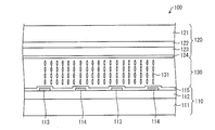
- FIG. 16 schematically shows the director distribution of the liquid crystal molecules in the liquid crystal cell when no voltage is applied in a typical liquid crystal panel using a display method in which a horizontal electric field is applied to the vertically aligned liquid crystal cell.
- FIG. 17 is a diagram schematically showing the director distribution of liquid crystal molecules in the liquid crystal cell when a voltage is applied.
- the liquid crystal cell 105 in the liquid crystal panel 100 using the display method typically has a liquid crystal layer 130 having a positive dielectric anisotropy sandwiched between a pair of substrates 110 and 120.
- One substrate 110 is provided with an insulating layer 112, a comb-like common electrode 113, a pixel electrode 114, and an alignment film 115 in this order on a glass substrate 111, and the other substrate 120 is provided on a glass substrate 121.
- the color filter 122, the dielectric layer 123, and the alignment film 124 are provided.
- alignment films 115 and 124 vertical alignment films for aligning the liquid crystal molecules 131 with the substrates 110 and 120 in the vertical direction when no voltage is applied are used.
- a voltage is applied between the common electrode 113 and the pixel electrode 114 that form a pair, thereby bending the liquid crystal panel.
- a two-domain different in director direction from each other by approximately 180 degrees is formed between the adjacent common electrode 113 and the pixel electrode 114, and accordingly, a wide viewing angle characteristic is formed. Can be realized.
- the liquid crystal panel 100 has the advantages of being able to obtain high-speed response based on bend alignment, a wide viewing angle due to a self-compensating arrangement, and high contrast due to vertical alignment, and has a simple structure and can be manufactured. It has the advantage of being easy and inexpensive to manufacture.
- Japanese Patent Publication Japanese Patent Laid-Open No. 11-316383 (published on November 16, 1999)”
- liquid crystal molecules in a region near the substrate 110 are easily affected by an electric field, but liquid crystal molecules in a region far from the substrate 110 are not easily affected by an electric field. Therefore, in order to influence the electric field on the liquid crystal molecules in the region far from the substrate 110, there arises a problem that the drive voltage must be increased.
- the present invention has been made in view of the above problems, and an object of the present invention is to improve the responsiveness of liquid crystal molecules in a liquid crystal panel and increase the transmittance without increasing the driving voltage.
- a liquid crystal panel according to the present invention is sandwiched between a first substrate and a second substrate that are arranged to face each other, and the first substrate and the second substrate.
- a liquid crystal panel wherein a common electrode and a pixel electrode are provided on the first substrate, and the liquid crystal layer is driven by an electric field generated between the common electrode and the pixel electrode.
- a first alignment film that orients liquid crystal molecules on the first substrate side of the liquid crystal layer obliquely with respect to the first substrate when no voltage is applied to a surface of the first substrate facing the second substrate.
- the liquid crystal molecules on the second substrate side of the liquid crystal layer are aligned perpendicularly to the second substrate when no voltage is applied.
- a second alignment film is provided.
- the present invention it is possible to improve the responsiveness of the liquid crystal molecules without increasing the driving voltage, and to realize a high transmittance of the liquid crystal panel and the liquid crystal display device.
- FIG. 1 is an exploded cross-sectional view schematically showing a schematic configuration of a liquid crystal display device according to Embodiment 1 of the present invention. It is a top view which shows an example of schematic structure of each electrode in the liquid crystal cell concerning Embodiment 1 of this invention, (a) is a top view which shows an example of schematic structure of the common electrode in an array substrate, (b) FIG. 3 is a plan view showing an example of a schematic configuration of pixel electrodes on an array substrate. 6 is a graph showing voltage-transmittance characteristics of Example 1 and a conventional example.
- FIG. 3 is a plan view showing an example of a schematic configuration of pixel electrodes on an array substrate. It is a graph which shows the voltage-transmittance characteristic of Example 2 and a prior art example.
- FIG. 1 It is a top view which shows an example of schematic structure of each electrode in the liquid crystal cell concerning the modification of this invention
- (a) is a top view which shows schematic structure of the common electrode in an array board
- (b) is a pixel in an array board
- FIG. 2B is a plan view showing an example of a schematic configuration of a pixel electrode in an array substrate
- FIG. 6 is a graph showing voltage-transmittance characteristics of Example 3 and a conventional example. It is sectional drawing which shows typically schematic structure of the liquid crystal cell in the liquid crystal panel concerning the modification of this invention with the director distribution of the liquid crystal molecule at the time of no voltage application.
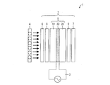
- FIG. 2 is an exploded sectional view schematically showing a schematic configuration of the liquid crystal display device according to the present embodiment.
- the liquid crystal display device 1 As shown in FIG. 2, the liquid crystal display device 1 according to the present embodiment is provided on the back side of the liquid crystal panel 2 (liquid crystal display panel, liquid crystal display element), the drive circuit 3 that drives the liquid crystal panel 2, and the liquid crystal panel 2. And a backlight 4 (illuminating device) for irradiating the liquid crystal panel 2 with light from the back side of the liquid crystal panel 2.
- the liquid crystal panel 2 liquid crystal display panel, liquid crystal display element
- the drive circuit 3 that drives the liquid crystal panel 2
- the liquid crystal panel 2 liquid crystal panel 2
- a backlight 4 illumination device for irradiating the liquid crystal panel 2 with light from the back side of the liquid crystal panel 2.
- the configurations of the drive circuit 3 and the backlight 4 are the same as the conventional ones. Therefore, the description of these configurations is omitted.
- the liquid crystal panel 2 includes a liquid crystal cell 5, polarizing plates 6 and 7, and retardation plates 8 and 9 as necessary.
- the liquid crystal panel 2 is formed by bonding polarizing plates 6 and 7 and, if necessary, retardation plates 8 and 9 to the liquid crystal cell 5.
- the polarizing plates 6 and 7 are respectively provided on the surfaces of the substrates 10 and 20 opposite to the surface facing the liquid crystal layer 30. Further, as shown in FIG. 2, the retardation plates 8 and 9 are provided between the substrates 10 and 20 and the polarizing plates 6 and 7 as necessary.
- the phase difference plates 8 and 9 may be provided only on one surface of the liquid crystal panel 2. Further, in the case of a display device using only front transmitted light, the retardation plates 8 and 9 are not necessarily essential.
- the polarizing plates 6 and 7 are, for example, electrode portions (branch electrodes) adjacent to each other through the slits in the electrodes having the transmission axes of the polarizing plates 6 and 7 orthogonal to each other and having slits provided in the liquid crystal cell 5. Are arranged such that the direction in which each is stretched and the transmission axis of the polarizing plates 6 and 7 form an angle of 45 °.
- the liquid crystal panel 2 is a vertical alignment type liquid crystal panel that is driven using a horizontal electric field as a horizontal electric field driving method. That is, the liquid crystal panel 2 includes a common electrode and a pixel electrode as a pair of electrodes on at least one of a pair of substrates provided to face each other, and is driven by an electric field generated in the lateral direction between the pair of electrodes. Is done. Further, in the liquid crystal panel 2, when no voltage is applied, in the liquid crystal cell 5, liquid crystal molecules located in the vicinity of the substrate having the common electrode and the pixel electrode are aligned (inclined) with a pretilt angle (initial alignment). At the same time, other liquid crystal molecules are aligned perpendicular to the substrate surface.
- the “vertical” includes “substantially vertical”.
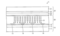
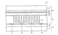
- FIG. 1 is a cross-sectional view schematically showing a schematic configuration of a main part of a liquid crystal cell 5 in a liquid crystal panel 2 according to the present embodiment, together with a director distribution of liquid crystal molecules when no voltage is applied.
- the liquid crystal cell 5 includes a pair of substrates 10 and 20 arranged to face each other as an array substrate (electrode substrate) and a counter substrate.
- a liquid crystal layer 30 is sandwiched between the substrates 10 and 20 as a display medium layer.
- At least one of these substrates 10 and 20, that is, at least the substrate on the viewer side, is a translucent substrate such as a glass substrate, preferably a transparent substrate, as an insulating substrate (liquid crystal layer holding member, base substrate). It has.
- a translucent substrate such as a glass substrate, preferably a transparent substrate, as an insulating substrate (liquid crystal layer holding member, base substrate). It has.
- a glass substrate is used as an insulating substrate will be described as an example, but this embodiment is not limited to this.
- the display surface side (observer side) substrate is described as the upper substrate, the other substrate is described as the lower substrate, and an array substrate is used as the lower substrate 10, and the upper substrate is used.
- a case where a counter substrate is used as the substrate 20 will be described as an example.
- the counter substrate may be a lower substrate and the array substrate may be an upper substrate.
- the substrate 10 (first substrate) is an array substrate as described above.
- a TFT substrate provided with a TFT (thin film transistor) as a switching element (not shown) can be used.
- an oxide semiconductor TFT (IGZO or the like) is preferably used for the TFT (thin film transistor) from the viewpoint of the transmittance improvement effect.
- An oxide semiconductor shows higher carrier mobility than amorphous silicon.
- the configuration of this embodiment is a vertical alignment mode using a lateral electric field driving method, and is particularly restricted by a display effective region in a pixel driven by liquid crystal molecules, so that the area of a transistor occupying one pixel is reduced.
- the substrate 10 includes, for example, an insulating layer 12 provided on a glass substrate 11, a common electrode 13 and a pixel electrode 14 provided on the insulating layer 12, and an alignment film 15 so as to cover these electrodes. (First alignment film) is provided.
- the common electrode 13 and the pixel electrode 14, which are a pair of electrodes, are electrodes each having a slit (space portion), and have a patterned electrode portion (electrode line) and a space portion (electrode non-forming portion). ing.
- the structures (shapes) of the common electrode 13 and the pixel electrode 14 will be described in detail later.
- the insulating layer 12 is formed in a solid shape over the entire display area of the substrate 10 so as to cover the substrate 10.
- the alignment film 15 is a so-called divided alignment film that aligns liquid crystal molecules 31 in the vicinity of the substrate 10 in the liquid crystal layer 30 obliquely with respect to the substrate surface when no voltage is applied.
- the alignment direction of the liquid crystal molecules 31 when no voltage is applied substantially coincides with the alignment direction when a voltage is applied.
- the alignment film 15 is formed in a solid shape on the insulating layer 12 so as to cover the common electrode 13 and the pixel electrode 14.
- the substrate 20 (second substrate) is a counter substrate. As shown in FIG. 1, the substrate 20 has a configuration in which, for example, a color filter 22, a dielectric layer 23, and an alignment film 24 (second alignment film) are stacked in this order on a glass substrate 21.
- the color filter 22 is provided with a color filter of each color such as R (red), G (green), and B (blue), a black matrix, and the like. That is, the substrate 20 may be a color filter substrate.
- the alignment film 24 is a so-called vertical alignment film that aligns liquid crystal molecules 31 adjacent to the substrate 20 in the liquid crystal layer 30 perpendicularly to the substrate surface when no voltage is applied. In the same manner that the alignment film 15 is formed in a solid shape over the entire display region of the substrate 10, the alignment film 24 is formed in a solid shape over the entire display region of the substrate 20.
- the substrates 10 and 20 may include an undercoat film or an overcoat film (not shown).
- the color filter 22 may be provided on the substrate 10 (first substrate, array substrate).
- ⁇ Liquid crystal layer 30> In the liquid crystal cell 5 in the liquid crystal panel 2, for example, the substrate 10 and the substrate 20 are bonded together by a sealant (not shown) through a spacer (not shown), and a liquid crystal is placed in the gap between the substrates 10 and 20. It is formed by enclosing a medium containing a material.
- the liquid crystal material may be a p (positive) type liquid crystal material or an n (negative) type liquid crystal material.
- the liquid crystal molecules in FIG. 1 show the case of a p (positive) type liquid crystal material.
- the liquid crystal panel 2 and the liquid crystal display device 1 form a distribution of electric field strength in the liquid crystal cell 5 by applying a voltage, thereby realizing a bend arrangement of the liquid crystal material.
- the liquid crystal material does not limit the values of the refractive index anisotropy ⁇ n and the dielectric anisotropy ⁇ , but preferably the refractive index anisotropy ⁇ n and the dielectric anisotropy ⁇ .
- the product ( ⁇ n ⁇ ⁇ ) is preferably 1.3 to 3.1.
- the common electrode 13 and the pixel electrode 14 for example, a transparent electrode material such as ITO (Indium / Tin / Oxide) or IZO (Indium / Zinc / Oxide) is preferably used.
- the substrate 10 is used as the substrate on the back side as described above, the common electrode 13 and the pixel electrode 14 are not necessarily transparent electrodes, and may be made of a metal electrode such as aluminum. Further, these electrodes may be formed of the same electrode material, or may be formed of different electrode materials.
- the method for forming (laminating) these electrodes is not particularly limited, and various conventionally known methods such as sputtering, vacuum deposition, and plasma CVD can be applied. Further, a method for patterning the common electrode 13 and the pixel electrode 14 is not particularly limited, and a known patterning method such as photolithography can be used.
- the film thickness of these electrodes is not particularly limited, but is preferably set within a range of 100 mm to 2000 mm.
- the film thickness of the insulating layer 12 depends on the type of the insulating layer 12 (for example, whether it is an inorganic insulating film or an organic insulating film), but is set, for example, within a range of 1000 to 30000 mm.
- the film thickness of the insulating layer 12 may be appropriately set according to the type of the insulating layer 12 and is not particularly limited, but the thinner one can be easily formed. However, the thickness of the insulating layer 12 is preferably 1000 mm or more from the viewpoint of preventing poor insulation due to defects and uneven film thickness.
- the method of forming (stacking) the insulating layer 12 is not particularly limited, and various conventionally known methods may be applied depending on the insulating material used, such as sputtering, vacuum deposition, plasma CVD, coating, and the like. Can do.
- the alignment film 15 is, for example, a polymer that can maintain the alignment control force of the alignment film material or the liquid crystal molecules having the split alignment control force so as to cover the common electrode 13 and the pixel electrode 14 on the insulating layer 12. It can form by apply
- the alignment film 24 can be formed, for example, by applying an alignment film material having a vertical alignment regulating force on the dielectric layer 23.
- each of the common electrode 13 and the pixel electrode 14 is a slit electrode having a slit (space portion), and has a patterned electrode portion (electrode line) and a space portion (electrode non-forming portion). is doing.
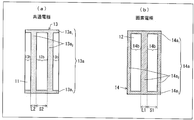
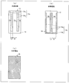
- FIG. 3A is a plan view showing a schematic configuration of the common electrode 13 and FIG. 3B is a schematic configuration of the pixel electrode 14.
- a so-called comb electrode having a comb-like structure is used as the common electrode 13 and the pixel electrode 14, respectively.
- the present embodiment is not limited to this.
- the common electrode 13 is a comb electrode having a patterned electrode portion 13a and a space portion 13b (slit), more specifically, a stem electrode. 13a 1 (stem line) and a branch electrode 13a 2 (branch line) corresponding to the teeth of a comb and extending from the stem electrode 13a 1 , and the branch electrode 13a 2 is spaced at a constant interval across the space portion 13b. It has the structure provided in. In FIG. 1, a cross section of the branch electrode 13 a 2 is illustrated as a cross section of the electrode portion 13 a of the common electrode 13.
- the pixel electrode 14 is a comb electrode having a patterned electrode portion 14a and a space portion 14b (slit), more specifically, It is composed of a stem electrode 14a 1 (stem line) and a branch electrode 14a 2 (branch line) corresponding to the teeth of a comb and extending from the stem electrode 14a 1 , and the branch electrode 14a 2 is constant across the space portion 14b. It has the structure provided by this space
- a cross section of the branch electrode 14 a 2 is illustrated as a cross section of the electrode portion 14 a of the pixel electrode 14.
- the electrode portion 14 a (particularly the branch electrode 14 a 2 ) of the pixel electrode 14 is disposed in the space portion 13 b of the common electrode 13.
- the electrode part 13 a (particularly the branch electrode 13 a 2 ) of the common electrode 13 is disposed in the space part 14 b of the pixel electrode 14.
- the electrode portion 13a (particularly the branch electrode 13a 2 ) of the common electrode 13 and the electrode portion 14a (particularly the branch electrode 14a 2 ) of the pixel electrode 14 are formed in positions and sizes that do not overlap each other.
- the number of teeth of the common electrode 13 and the pixel electrode 14 (that is, the branch electrodes 13a 2 and 14a 2 constituting the electrode portions 13a and 14a) provided in one pixel is not particularly limited, It is determined in relation to each L / S in the common electrode 13 and the pixel electrode 14.
- L is the electrode width of the line electrode, and indicates the electrode width of each of the branch electrodes 13a 2 and 14a 2 .
- S is an electrode interval, and indicates an electrode interval between adjacent branch electrodes 13a 2 and 13a 2 or an electrode interval between adjacent branch electrodes 14a 2 and 14a 2 . That is, S indicates the width of the space portions 13b and 14b.
- the liquid crystal molecules 31 above the common electrode 13 and the pixel electrode 14 are hardly affected by the electric field, and therefore light does not pass through the display principle. For this reason, it is preferable that the electrode width L1 of the branch electrode 14a 2 and the electrode width L2 of the branch electrode 13a 2 are smaller. However, the case where the common electrode 13 or the pixel electrode 14 is a solid electrode is excluded.
- the smallest electrode width that can be produced is technically 2 ⁇ m. Therefore, the electrode widths L1 and L2 are preferably in the range of 2 ⁇ m to 5 ⁇ m, more preferably in the range of 2 ⁇ m to 3 ⁇ m in consideration of errors. However, in the future, the lower limit of the electrode widths L1 and L2 is not limited to this.
- the electrode spacings S1 and S2 are not particularly limited, but are preferably 4 ⁇ m or more and 12 ⁇ m or less from the viewpoint of the aperture ratio.
- the electrode spacing S1 is not limited to the above range as long as sufficient substantial transmittance can be obtained even if it exceeds 12 ⁇ m, for example.
- Each of the branch electrodes 13a 2 and 14a 2 may be formed in a straight line, or may be formed in a V shape or a zigzag shape.
- the liquid crystal panel 2 according to the present embodiment is a vertical alignment type liquid crystal panel that is driven using a lateral electric field.
- the liquid crystal panel 2 has a configuration in which a split alignment film is provided as the alignment film 15 on the surface of the substrate 10 and a vertical alignment film is provided as the alignment film 24 on the surface of the substrate 20.
- a split alignment film is provided as the alignment film 15 on the surface of the substrate 10
- a vertical alignment film is provided as the alignment film 24 on the surface of the substrate 20.
- the self-director has a central portion of the branch electrode 13a 2 that is an electrode line in the common electrode 13 and a central portion of the branch electrode 14a 2 that is an electrode line in the pixel electrode 14 Are arranged so as to compensate for cancellation.
- the liquid crystal panel 2 is caused by the high-speed response based on the bend alignment, which is an effect peculiar to the vertical alignment type liquid crystal panel using the horizontal electric field driving method, the wide viewing angle due to the self-director canceling compensation arrangement, and the vertical alignment High contrast can be realized.
- the common electrode 13 and the pixel electrode 14 which are a pair of electrodes are provided on the same substrate, and the liquid crystal molecules 31 near the substrate 10 have a pretilt angle when no voltage is applied. Since the liquid crystal molecules are easily moved when a voltage is applied, the responsiveness of the liquid crystal molecules 31 in the liquid crystal panel 2 is improved as a whole liquid crystal layer. Therefore, the transmittance can be increased while lowering the voltage.
- the pixel electrode 14 is a drain electrode (not shown) and is connected to a signal line and a switching element such as a TFT (including an oxide semiconductor TFT), and a signal corresponding to the video signal is applied.
- a switching element such as a TFT (including an oxide semiconductor TFT), and a signal corresponding to the video signal is applied.
- the common electrode 13 is set to 0 V, and the voltage applied to the pixel electrode 14 is changed. Note that each of the branch electrodes 14a 2 of the pixel electrodes 14 are all the same voltage is applied.
- liquid crystal panel 2 display is performed by applying a potential difference between the common electrode 13 and the pixel electrode 14. Due to this potential difference, a horizontal electric field is generated between the pixel electrode 14 and the common electrode 13, and the lines of electric force between the pixel electrode 14 and the common electrode 13 are curved in a semicircular shape.
- the liquid crystal molecules 31 are arranged according to the electric field strength distribution in the liquid crystal cell 5 and the binding force from the interface.
- the liquid crystal molecules 31 are rotated by the horizontal electric field generated between the pixel electrode 14 and the common electrode 13, thereby controlling the amount of light transmitted through the liquid crystal panel 2 and performing display. .
- ⁇ Orientation control method> Hereinafter, in the liquid crystal panel 2, a method for controlling the alignment (divided alignment) of the liquid crystal molecules 31 in the vicinity of the substrate 10 when no voltage is applied will be specifically described.
- an alignment film material diluted in a solvent is applied on a substrate by a printing method, an ink jet method, a spin coater method or the like so as to obtain a desired film thickness. Thereafter, the substrate is heated in an atmosphere necessary for solvent drying to form an alignment film. Thereafter, the substrate on which the alignment film is formed is irradiated with polarized light that reacts with the photoreactive functional group from a desired direction so that the liquid crystal molecules 31 are inclined in the same direction as the electric field is applied. Do it once.
- the desired gap is maintained and the liquid crystal layer 30 is sandwiched. Thereby, only the liquid crystal molecules 31 near the substrate 10 are divided and aligned when no voltage is applied.
- substrate 10 should just be irradiation of 1 J / cm ⁇ 2 > @ 335 nm or less using the high pressure mercury lamp etc. which generate
- vision orientation method 2 Further, another method using an alignment film having a photoreactive functional group such as a cinnamate group (chemical structure 1) in the side chain of the side chain polymer as the alignment film 15 and exhibiting vertical alignment will be described below. .
- an alignment film material diluted in a solvent is applied on a substrate by a printing method, an ink jet method, a spin coater method or the like so as to obtain a desired film thickness. Thereafter, the substrate is heated in an atmosphere necessary for solvent drying, and an alignment film 15 made of a side chain polymer having a photoreactive functional group in the side chain is formed on the substrate.
- the liquid crystal panel 2 is formed while holding a desired gap and sandwiching the liquid crystal layer 30.
- the alignment film 15 made of a side chain polymer having a photoreactive functional group in the side chain is used to irradiate light that reacts with the photoreactive functional group, and the vicinity of the substrate 10
- the liquid crystal molecules 31 are processed so as to maintain the alignment. Thereby, only the liquid crystal molecules 31 near the substrate 10 are divided and aligned when no voltage is applied.
- the light irradiated to the liquid crystal panel 2 should just be irradiation of 1 J / cm ⁇ 2 > @ 335 nm or less using the high pressure mercury lamp etc. which generate
- a vertical alignment film material diluted in a solvent is applied on a substrate by a printing method, an ink jet method, a spin coater method or the like so as to have a desired film thickness. Thereafter, the substrate is heated in a temperature atmosphere necessary for solvent drying to form an alignment film 15 exhibiting vertical alignment on the substrate.
- the substrate 10 on which the alignment film 15 is formed and the substrate 20 opposite to the substrate 10 are used to hold a liquid crystal layer 30 containing a photoreactive monomer (for example, chemical structure 2) while maintaining a desired gap.
- a photoreactive monomer for example, chemical structure 2
- a voltage is applied to the common electrode 13 and the pixel electrode 14 of the liquid crystal panel 2. Then, in a state where this voltage is applied, light that reacts with the photoreactive monomer is irradiated to perform the treatment so as to maintain the alignment of the liquid crystal molecules 31 in the vicinity of the substrate 10 (PSA treatment). Thereby, only the liquid crystal molecules 31 near the substrate 10 are divided and aligned.
- the light irradiated to the liquid crystal panel 2 by PSA processing should just be irradiation of 1 J / cm ⁇ 2 > @ 335 nm or less using the high pressure mercury lamp etc. which generate
- the light for reacting the photoreactive functional group or photoreactive monomer may be irradiated from either the substrate 10 or the substrate 20 side.
- SiN silicon nitride
- each of branch electrodes 14a 2 of the pixel electrode 14 to form the pixel electrode 14 so as to be positioned at the center between the branch electrodes 13a 2 of the common electrode 13.
- the photo-alignment film having the above-described vertical alignment was applied on the insulating layer 12 by a spin coating method so as to cover the common electrode 13 and the pixel electrode 14. Then, the board
- SiN silicon nitride
- a photo-alignment film having a vertical alignment similar to that on the substrate 10 side was applied on the dielectric layer 23 by a spin coating method. Thereafter, the substrate 20 having the alignment film 24 as a vertical alignment film provided on the dielectric layer 23 was formed by baking at about 200 ° C. for about 2 hours.
- the dry film thicknesses of the alignment films 15 and 24 were both about 1000 mm.
- plastic beads were dispersed as spacers on one of the substrates 10 and 20.
- an epoxy thermosetting resin was printed as a sealing agent on the other substrate facing the one substrate.
- the substrates 10 and 20 were bonded to each other and baked at about 150 ° C. for about 1 hour, thereby producing a liquid crystal cell 5.
- the retardation (d ⁇ ⁇ n) was set so as to be approximately 1 / 2 ⁇ .
- the pretilt angle of the liquid crystal molecules 31 in the vicinity of the substrate 10 was controlled to 88.5 °, and the pretilt angle of the liquid crystal molecules 31 in the vicinity of the substrate 20 was controlled to 90 °.
- the liquid crystal panel 2 thus fabricated was mounted on the backlight 4 and driven as shown in FIG. 2, and the change in voltage-transmittance on the front surface of the liquid crystal panel 2 was measured with a luminance meter. .
- the transmittance was obtained from the luminance of the liquid crystal panel 2 / the luminance of the backlight 4.
- FIG. 4 is a graph of voltage-transmittance characteristics showing the measurement results.
- SiN silicon nitride
- a photo-alignment film having a vertical alignment property was applied on the insulating layer 112 by a spin coat method so as to cover the common electrode 113 and the pixel electrode 114. Then, the board
- SiN silicon nitride
- the substrate 120 was formed by forming an alignment film 124 as a vertical alignment film on the dielectric layer 123 by the same material and the same process as the alignment film 115.
- the dry thickness of the alignment films 115 and 124 thus obtained was about 1000 mm.
- plastic resin beads were dispersed as spacers on one of the substrates 110 and 120 in the same manner as in Example 1.
- an epoxy-based thermosetting resin as a sealing resin was printed as a sealing agent on the other substrate facing the one substrate.
- the substrates 110 and 120 were bonded together and baked at about 150 ° C. for about 1 hour as in Example 1 to fabricate the liquid crystal cell 105.
- the retardation (d ⁇ ⁇ n) was set so as to be approximately a 1 / 2 ⁇ condition as in Example 1.
- the pretilt angle of all the liquid crystal molecules 31 was 90 °.
- a polarizing plate (not shown) similar to that of Example 1 is formed on the front and back surfaces of the liquid crystal cell 105, the transmission axis of the polarizing plate is orthogonal, and the direction in which each branch electrode is extended and the polarizing plate Bonding was performed so that the transmission axis formed an angle of 45 °.
- a comparative (conventional) liquid crystal panel 100 liquid crystal display element having the configuration shown in FIG. 16 was produced.
- the liquid crystal panel 100 thus manufactured was measured in the same manner as in Example 1.
- the graph of FIG. 4 shows voltage-transmittance characteristics indicating the measurement results of the conventional example.
- the transmittance when 5 V is applied is 16.0% in the liquid crystal panel 100 of the conventional example, whereas 23.4 in the liquid crystal panel 2 of the first embodiment. %, And the transmittance was improved by 7.4%.
- the applied voltage for obtaining a transmittance of 5% is 4.3 V in the liquid crystal panel 100 of the conventional example, whereas it is 3.2 V in the liquid crystal panel 2 of the first embodiment. It decreased by 1V.
- the liquid crystal panel of Example 1 it was confirmed that high transmittance and low voltage can be realized.
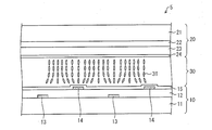
- FIG. 5 is a cross-sectional view schematically showing the schematic configuration of the main part of the liquid crystal cell 5 of the liquid crystal panel 2 according to the present embodiment, together with the director distribution of liquid crystal molecules when no voltage is applied.
- FIG. 6A is a plan view showing a schematic configuration of the common electrode 13 which is a lower layer electrode
- FIG. 6B is a plan view showing a schematic configuration of the pixel electrode 14 which is an upper layer electrode.
- the liquid crystal panel 2 according to the present embodiment is common to the substrate 10 below the pixel electrode 14 in the liquid crystal panel 2 shown in FIG.
- the electrode 13 has a configuration with a solid common electrode. That is, the substrate 10 is provided with a solid common electrode 13, an insulating layer 12, a comb-like pixel electrode 114, and an alignment film 15 in this order on a glass substrate 11. That is, in the substrate 10, the insulating layer 12 is provided between the common electrode 13 and the pixel electrode 14, the common electrode 13 is provided on the lower layer side of the insulating layer 12, and the pixel electrode 14 is provided on the upper layer side of the insulating layer 12. It has been.
- the cross section of the branch electrode 14 a 2 is illustrated as the cross section of the electrode portion 14 a of the pixel electrode 14.
- the branch electrode 14a 2 may be formed in a straight line shape, or may be formed in a V shape or a zigzag shape.
- Example 2 In Example 1, instead of the comb-like common electrode 12, except that the solid common electrode 12 made of ITO was formed on the entire surface of one side of the glass substrate 11 with a thickness of 1400 mm by sputtering. This is the same as the liquid crystal panel 2 of the first embodiment.
- the retardation (d ⁇ ⁇ n) was set so as to be approximately 1 / 2 ⁇ .
- the pretilt angle of the liquid crystal molecules 31 in the vicinity of the substrate 10 was controlled to 88.5 °, and the pretilt angle of the liquid crystal molecules 31 in the vicinity of the substrate 20 was controlled to 90 °.
- the liquid crystal panel 2 produced in this manner was measured in the same manner as in Example 1.
- FIG. 7 is a graph of voltage-transmittance characteristics showing the measurement results.
- the graph of FIG. 7 also shows the voltage-transmittance characteristics showing the measurement results of the conventional example.
- Example 2 a table summarizing numerical values obtained by reading the transmittance when the applied voltage is 5 V and the applied voltage at which the transmittance is 5% in Example 2 and the conventional example in the graph shown in FIG. 7 is shown below.
- the transmittance when 5 V is applied is 15.2% in the liquid crystal panel 100 of the conventional example, whereas 17.5 in the liquid crystal panel 2 of the second embodiment. %, And the transmittance was improved by 2.3%.
- the applied voltage for obtaining a transmittance of 5% is 2.44 V in the liquid crystal panel 100 of the conventional example, whereas it is 2.14 V in the liquid crystal panel 2 of the second embodiment, and the applied voltage is 0. It decreased by 3V.
- the common electrode 13 and the pixel electrode 14 are slit electrodes each having a slit (space portion), and are patterned electrode portions (electrode lines) and A comb electrode having a space portion (electrode non-forming portion) may be used.
- the common electrode 13 and the pixel electrode 14 may be an electrode having an opening (slit) at the center of a solid electrode (surface electrode) as an electrode having a slit (space part). This specific example will be described below.
- FIG. 8A is a plan view showing a schematic configuration of the common electrode 13 and FIG. 8B is a schematic configuration of the pixel electrode 14, and FIG. 9 is a cross-sectional view of the liquid crystal panel 2 of the present modification.
- the common electrode 13 and the pixel electrode 14 shown in FIGS. 3A and 3B are formed as a space portion at one end by making a plurality of cuts in the solid electrode from one end to the other opposite end.
- the common electrode 13 and the pixel electrode 14 shown in FIGS. 8A and 8B have a comb-like shape having a plurality of notches (slits). A plurality of openings (opening windows, slits) are provided as space portions, and each end portion is connected.
- the common electrode 13 in this modification includes a frame-shaped (frame-shaped) stem electrode 13a 1 and a frame-shaped stem electrode as patterned electrode portions 13a.
- 13a 1 has a striped branch electrode 13a 2 (branch line) extending from one end to the other opposite end, and the branch electrode 13a 2 is provided at a constant electrode interval across the space portion 13b. is doing.
- the pixel electrode 14 in the present modification as shown in FIG. 8 (b), as patterned electrode portions 14a, and the stem electrodes 14a 1 of the frame-shaped (frame-shaped), the frame-shaped stem
- the electrode 14a 1 has a striped branch electrode 14a 2 (branch line) extending from one end to the other opposite end, and the branch electrode 14a 2 is provided at a constant electrode interval with the space portion 14b interposed therebetween.
- the branch electrode 14a 2 of the pixel electrode 14 is disposed in the space 13b of the common electrode 13, and the position and size (electrode width) of the common electrode 13 that do not overlap with the branch electrode 13a 2 Is formed.
- each of the branch electrodes 13a 2 and 14a 2 may be formed in a linear shape, or may be formed in a V shape or a zigzag shape.
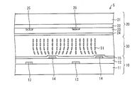
- FIG. 10 is a cross-sectional view schematically showing the schematic configuration of the main part of the liquid crystal cell 5 of the liquid crystal panel 2 according to the present embodiment, together with the director distribution of liquid crystal molecules when no voltage is applied.
- FIG. 11A is a plan view showing a schematic configuration of the common electrode 13
- FIG. 11B is a plan view showing a schematic configuration of the pixel electrode 14
- FIG. 3 is a plan view showing a schematic configuration of a substrate side electrode (counter electrode) 25.
- FIG. 11A is a plan view showing a schematic configuration of the common electrode 13
- FIG. 11B is a plan view showing a schematic configuration of the pixel electrode 14
- FIG. 3 is a plan view showing a schematic configuration of a substrate side electrode (counter electrode) 25.
- the liquid crystal panel 2 according to the present embodiment is similar to the liquid crystal panel 2 shown in FIG. 1 according to the first embodiment, as shown in FIGS.
- the counter electrode 25 includes a solid electrode. That is, the substrate 20 is provided with a color filter 22, a solid counter electrode 25, a dielectric layer 23, and an alignment film 24 in this order on a glass substrate 21.
- the cross sections of the branch electrode 13 a 2 and the branch electrode 14 a 2 are illustrated as cross sections of the electrode portion 13 a of the common electrode 13 and the electrode portion 14 a of the pixel electrode 14.
- the branch electrode 13a 2 and the branch electrode 14a 2 may be formed in a straight line shape, or may be formed in a V shape or a zigzag shape.
- a voltage is applied to the common electrode 13 and the pixel electrode 14, and an intermediate voltage value of the voltage applied to the common electrode 13 and the pixel electrode 14 is applied to the counter electrode 25.
- the state where this voltage is applied light that reacts with the photoreactive monomer is irradiated to perform the treatment so as to maintain the alignment of the liquid crystal molecules 31 in the vicinity of the substrate 10 (PSA treatment).
- PSA treatment light that reacts with the photoreactive monomer is irradiated to perform the treatment so as to maintain the alignment of the liquid crystal molecules 31 in the vicinity of the substrate 10
- the liquid crystal panel 2 in which only the alignment of 31 is divided and formed is prepared.
- a configuration in which no voltage is applied to the counter electrode 25 may be employed.
- Example 3 In Example 1, the same as the liquid crystal panel 2 of Example 1 except that the solid counter electrode 25 made of ITO was formed by sputtering on the color filter 22 of the glass substrate 20 with a thickness of 1400 mm. It is. In the liquid crystal panel 2 of Example 3, the retardation (d ⁇ ⁇ n) was set so as to be approximately 1 / 2 ⁇ . Further, as in Example 1, the pretilt angle of the liquid crystal molecules 31 in the vicinity of the substrate 10 was controlled to 88.5 °, and the pretilt angle of the liquid crystal molecules 31 in the vicinity of the substrate 20 was controlled to 90 °.
- the liquid crystal panel 2 produced in this manner was measured in the same manner as in Example 1.
- FIG. 12 is a graph of voltage-transmittance characteristics showing the measurement results.
- the graph of FIG. 12 also shows voltage-transmittance characteristics indicating the measurement results of the conventional example.
- Example 3 a table summarizing numerical values obtained by reading the transmittance when the applied voltage is 5 V and the applied voltage at which the transmittance is 5% in Example 3 and the conventional example in the graph shown in FIG. 12 is shown below.
- the transmittance when 5 V is applied is 14.6% in the liquid crystal panel 100 of the conventional example, whereas 23.7 in the liquid crystal panel 2 of the third embodiment. %, And the transmittance was improved by 9.1%.
- the applied voltage for obtaining a transmittance of 5% is 3.3 V in the liquid crystal panel 100 of the conventional example, whereas it is 2.0 V in the liquid crystal panel 2 of Example 3, and the applied voltage is 1. It decreased by 3V.
- the liquid crystal panel of Example 3 it was confirmed that high transmittance and low voltage can be realized.
- the counter electrode 25 includes the common electrode 13 and the pixel electrode 15.
- a configuration using comb electrodes may be used.
- the branch electrode 25a 2 of the counter electrode 25 is disposed immediately above the branch electrode 13a 2 of the common electrode 13, and the position and size (electrode width) of the pixel electrode 14 that do not overlap with the branch electrode 14a 2 Formed.
- 14A is a plan view showing a schematic configuration of the common electrode 13
- FIG. 14B is a plan view showing a schematic configuration of the pixel electrode 14
- FIG. 14C is a counter electrode 25. As shown in FIG. It is a top view which shows schematic structure of these.
- the liquid crystal panel 2 of FIG. 13 may have a configuration in which the common electrode 13 is provided below the pixel electrode 14.
- the branch electrode 13a 2 of the common electrode 13 is disposed directly below the center of the space portion 14b of the pixel electrode 14 (directly below the center of the opening), and does not overlap with the branch electrode 14a 2 of the pixel electrode 14.
- it is formed in a size (electrode width).
- a liquid crystal panel according to the present invention includes a first substrate and a second substrate disposed to face each other, and a liquid crystal layer sandwiched between the first substrate and the second substrate.
- a liquid crystal panel in which a common electrode and a pixel electrode are provided on the substrate, and the liquid crystal layer is driven by an electric field generated between the common electrode and the pixel electrode, and the second substrate in the first substrate A first alignment film for obliquely aligning liquid crystal molecules on the first substrate side in the liquid crystal layer with respect to the first substrate when no voltage is applied to the surface facing the second substrate;
- a second alignment film for aligning liquid crystal molecules on the second substrate side of the liquid crystal layer perpendicularly to the second substrate when no voltage is applied is provided on a surface of the liquid crystal layer facing the first substrate. It is the composition which is.
- the liquid crystal panel has a high-speed response based on the bend alignment, which is an effect peculiar to the vertical alignment type liquid crystal panel using the lateral electric field driving method, a wide viewing angle due to the self-director canceling compensation arrangement, and a vertical High contrast resulting from orientation can be realized.
- liquid crystal panel a common electrode and a pixel electrode which are a pair of electrodes are provided on a first substrate, and liquid crystal molecules near the first substrate are obliquely aligned when no voltage is applied (pretilt). Therefore, the liquid crystal molecules easily move when a voltage is applied, and the responsiveness of the liquid crystal molecules in the liquid crystal panel is improved as a whole liquid crystal layer. Therefore, the transmittance can be increased while lowering the voltage.
- the first alignment film preferably aligns liquid crystal molecules on the first substrate side in a direction of an electric field generated when a voltage is applied when no voltage is applied.
- the common electrode and the pixel electrode may be provided in the same layer in the first substrate.
- an insulating layer is provided between the common electrode and the pixel electrode in the first substrate, the common electrode is provided on a lower layer side of the insulating layer, and the pixel electrode is insulated from the insulating layer. It may be provided on the upper layer side of the layer.
- a counter electrode is provided on the second substrate, and the liquid crystal layer is driven by an electric field generated between the pixel electrode, the common electrode, and the counter electrode.
- the liquid crystal molecules in the region close to the second substrate are easily affected by the electric field, so that the voltage can be further reduced.
- the counter electrode may be provided between the color filter and the dielectric layer.
- the liquid crystal molecules may have a positive dielectric anisotropy.
- the first alignment film is preferably a photo-alignment film having a photoreactive functional group in the side chain of the side chain polymer.
- the photo-reactive functional group of the first alignment film is irradiated with polarized light that reacts with the photo-reactive functional group of the first alignment film, or the voltage is applied to the liquid crystal panel including the first alignment film.
- polarized light that reacts with the photo-reactive functional group of the first alignment film
- the voltage is applied to the liquid crystal panel including the first alignment film.
- a polymer layer that maintains the alignment regulating force of liquid crystal molecules may be formed on the side of the first alignment film in contact with the liquid crystal layer.
- the liquid crystal molecules in the vicinity of the first substrate can be subjected to alignment treatment (alignment control).
- the polymer layer may be formed of a photoreactive monomer mixed in a liquid crystal material.
- the above-mentioned photoreactive monomer reacts with the light that reacts, and the liquid crystal on the side in contact with the liquid crystal layer in the first alignment film
- the molecules can be subjected to orientation treatment (orientation control).
- each of the common electrode and the pixel electrode is a slit electrode in which a plurality of branch electrodes extending from the trunk electrode are provided with a constant electrode interval across the slit, and is viewed from a direction perpendicular to each substrate. It is preferable that the branch electrode in the common electrode is disposed between adjacent branch electrodes in the pixel electrode.
- the slit electrode may be a comb electrode.
- the pixel electrode is a slit electrode in which a plurality of branch electrodes extending from the stem electrode are provided at a constant electrode interval across the slit, and the slit electrode includes a frame-shaped stem electrode and a frame-shaped electrode And a striped branch electrode extending from one end of the main electrode to the opposite opposite end, and the branch electrode may be a slit electrode provided at a constant electrode interval with a slit interposed therebetween.
- the common electrode may be a solid electrode.
- the liquid crystal display device includes any of the liquid crystal panels described above.
- the liquid crystal panel and the liquid crystal display device according to the present invention have high liquid crystal molecule responsiveness and high transmittance at a practical driving voltage. Moreover, wide viewing angle characteristics equivalent to those of the MVA mode and IPS mode, high-speed response comparable to or higher than the OCB mode, and high contrast characteristics can be realized at the same time. Therefore, it can be particularly suitably used for public bulletin boards for outdoor use, mobile devices such as mobile phones and PDAs.
Landscapes
- Physics & Mathematics (AREA)
- Nonlinear Science (AREA)
- Mathematical Physics (AREA)
- Chemical & Material Sciences (AREA)
- Crystallography & Structural Chemistry (AREA)
- General Physics & Mathematics (AREA)
- Optics & Photonics (AREA)
- Geometry (AREA)
- Spectroscopy & Molecular Physics (AREA)
- Liquid Crystal (AREA)
Abstract
液晶パネル(2)は、基板(10)に、電圧無印加時に基板(10)側の液晶分子(31)を斜めに配向させる分割配向膜(15)が設けられ、基板(20)に垂直配向膜(24)が設けられている。
Description
本発明は液晶パネルおよび液晶表示装置に関するものであり、より詳しくは、電圧無印加時に液晶分子が基板垂直方向に配向する垂直配向型の液晶セルに横電界を印加することで光の透過を制御する液晶パネルおよび該液晶パネルを備えた液晶表示装置に関するものである。
液晶表示装置は、各種表示装置のなかでも薄型で軽量かつ消費電力が小さいといった利点を有している。このため、近年、CRT(陰極線管)に代わって、TV(テレビション)、モニタ、携帯電話等のモバイル機器等の様々な分野で広く用いられている。
液晶表示装置の表示方式は、液晶セル内で液晶をどのように配列させるかによって決定される。液晶表示装置の表示方式としては、各種表示方式が知られている。
そのなかの一つとして、画素構成が単純で、かつ、優れた視野角特性を有し、垂直配向による高コントラスト性を得ることができる表示方式として、電圧無印加時に液晶分子が基板に垂直方向に配向する垂直配向型の液晶セルを使用し、同一基板上に形成された第1電極および第2電極に電圧を印加して電位差を与えることで生じる電気場によって液晶分子を再配列させて表示を行う表示方式が知られている(例えば、特許文献1)。
以下に、このように同一基板上に形成された第1電極と第2電極との間に生じる横向きの電界(横電界)により表示を行ういわゆる横電界駆動方式を用いた垂直配向型の液晶パネルにおける典型的なセル構成について説明する。
図16は、このように垂直配向型の液晶セルに横電界を印加する表示方式を用いた典型的な液晶パネルにおいて、電圧無印加時の液晶セル内の液晶分子のダイレクタ分布を模式的に示す図であり、図17は、電圧印加時の液晶セル内の液晶分子のダイレクタ分布を模式的に示す図である。
図17に示すように、上記表示方式を用いた液晶パネル100における液晶セル105は、典型的には、一対の基板110・120間に、誘電率異方性が正の液晶層130が挟持され、一方の基板110は、ガラス基板111上に、絶縁層112、櫛歯状の共通電極113および画素電極114、配向膜115がこの順に設けられ、他方の基板120は、ガラス基板121上に、カラーフィルタ122、誘電体層123および配向膜124が設けられた構成を有している。
配向膜115・124には、電圧無印加時に液晶分子131を基板110・120に垂直方向に配向させる垂直配向膜が使用される。
上記したように横電界駆動方式を用いた垂直配向型の液晶パネル100においては、図17に示すように、対となる共通電極113と画素電極114との間に電圧を印加することで、ベンド状(弓なり状)の電界が形成され、隣り合う共通電極113と画素電極114との間に、互いにダイレクタ方位が略180度異なる2つのドメインが形成されるとともに、これに伴い、広い視野角特性を実現することができる。
したがって、液晶パネル100は、ベンド配向に基づく高速応答性、自己補償型配列による広視野角、垂直配向に起因する高コントラストを得ることができるという利点を有するとともに、構造がシンプルであり、製造が容易で、安価に製造することができるという利点を有している。
しかしながら、このような液晶パネル100では、アレイ基板である一方の基板110に設けられた対の電極間のみで電界を発生させている。
このため、基板110に近い領域の液晶分子は電界の影響を受け易いが、基板110から遠い領域の液晶分子は電界の影響を受け難い。よって、基板110から遠い領域の液晶分子に対しても電界の影響を与えるためには、駆動電圧を高めなければならないという問題が生じる。
本発明は、上記問題点に鑑みなされたものであり、その目的は、駆動電圧を高めることなく、液晶パネルにおける液晶分子の応答性を向上させて高透過率化を実現することにある。
本発明にかかる液晶パネルは、上記の課題を解決するために、互いに対向配置された第1の基板および第2の基板と、上記第1の基板と第2の基板との間に挟持された液晶層とを備え、上記第1の基板に共通電極および画素電極が設けられ、上記液晶層が上記共通電極と画素電極との間に発生する電界で駆動される液晶パネルであって、上記第1の基板における上記第2の基板に対向する面に、電圧無印加時に上記液晶層における該第1の基板側の液晶分子を該第1の基板に対して斜めに配向させる第1の配向膜が設けられ、上記第2の基板における上記第1の基板に対向する面に、電圧無印加時に上記液晶層における該第2の基板側の液晶分子を該第2の基板に対して垂直に配向させる第2の配向膜が設けられていることを特徴とする。
本発明によれば、駆動電圧を高めることなく液晶分子の応答性を向上させ、液晶パネルおよび液晶表示装置の高透過率化を実現することができる。
以下に、本発明について詳細に説明する。
〔実施の形態1〕
本発明の実施の一形態について図1~図4に基づいて説明すれば以下の通りである。
本発明の実施の一形態について図1~図4に基づいて説明すれば以下の通りである。
<液晶表示装置の概略構成>
まず、本実施の形態にかかる液晶表示装置の全体の概略構成について説明する。
まず、本実施の形態にかかる液晶表示装置の全体の概略構成について説明する。
図2は、本実施の形態にかかる液晶表示装置の概略構成を模式的に示す分解断面図である。
本実施の形態にかかる液晶表示装置1は、図2に示すように、液晶パネル2(液晶表示パネル、液晶表示素子)、液晶パネル2を駆動する駆動回路3、液晶パネル2の背面側に設けられ、液晶パネル2の背面側から液晶パネル2に光を照射するバックライト4(照明装置)を備えている。
なお、駆動回路3およびバックライト4の構成は従来と同じである。したがって、これらの構成については、その説明を省略する。
<液晶パネル2の概略構成>
次に、液晶パネル2の全体の概略構成について説明する。
次に、液晶パネル2の全体の概略構成について説明する。
図2に示すように、液晶パネル2は、液晶セル5と、偏光板6・7と、必要に応じて位相差板8・9と、を備えている。液晶パネル2は、液晶セル5に、偏光板6・7および必要に応じて位相差板8・9を貼り合わせることにより形成される。
偏光板6・7は、基板10・20における液晶層30との対向面とは反対側の面にそれぞれ設けられる。また、位相差板8・9は、図2に示すように、例えば、基板10・20と偏光板6・7との間に、必要に応じて設けられる。なお、位相差板8・9は、液晶パネル2の一方の面にのみ設けられていてもよい。また、正面透過光のみを利用する表示装置の場合には、位相差板8・9は必ずしも必須ではない。
偏光板6・7は、例えば、偏光板6・7の透過軸が互いに直交し、かつ、液晶セル5に設けられたスリットを有する電極における、スリットを介して隣り合う各電極部(枝電極)がそれぞれ延伸される方向と偏光板6・7の透過軸とが45゜の角度をなすように配置される。
液晶パネル2は、横電界駆動方式として横電界を用いて駆動を行う垂直配向型の液晶パネルである。すなわち、液晶パネル2は、互いに対向して設けられた対の基板のうち少なくとも一方の基板に対の電極として共通電極および画素電極を備え、これら対の電極間に横方向に発生する電界によって駆動される。また、液晶パネル2は、電圧無印加時に、液晶セル5において、共通電極および画素電極を備えた基板の近傍に位置する液晶分子がプレチルト角を有して(斜めに)配向(初期配向)するとともに、それ以外の液晶分子が基板面に垂直に配向している。なお、上記「垂直」には「略垂直」も含まれる。
以下に、液晶セル5の概略構成について説明する。
<液晶セル5の概略構成>
図1は、本実施の形態にかかる液晶パネル2における液晶セル5の要部の概略構成を、電圧無印加時における液晶分子のダイレクタ分布と併せて模式的に示す断面図である。
図1は、本実施の形態にかかる液晶パネル2における液晶セル5の要部の概略構成を、電圧無印加時における液晶分子のダイレクタ分布と併せて模式的に示す断面図である。
図1に示すように、液晶セル5は、アレイ基板(電極基板)および対向基板として、互いに対向して配置された一対の基板10・20を備えている。これら基板10・20間には、表示用の媒質層として液晶層30が挟持されている。
これら基板10・20のうち少なくとも一方の基板、つまり、少なくとも観察者側の基板は、絶縁基板(液晶層保持部材、ベース基板)として、ガラス基板等の透光性基板、好適には透明基板、を備えている。以下、本実施の形態では、絶縁基板として、それぞれガラス基板を用いた場合を例に挙げて説明するが、本実施の形態はこれに限定されるものではない。
また、以下の説明では、表示面側(観察者側)の基板を上側の基板とし、他方の基板を下側の基板として説明するとともに、下側の基板10としてアレイ基板を使用し、上側の基板20として対向基板を使用した場合を例に挙げて説明する。
しかしながら、本実施の形態はこれに限定されるものではなく、対向基板を下側の基板とし、アレイ基板を上側の基板としても構わない。
次に、液晶セル5における各構成について説明する。
<基板10>
基板10(第1の基板)は上記したようにアレイ基板である。基板10としては、例えば、図示しないスイッチング素子としてTFT(薄膜トランジスタ)が設けられたTFT基板等を用いることができる。
基板10(第1の基板)は上記したようにアレイ基板である。基板10としては、例えば、図示しないスイッチング素子としてTFT(薄膜トランジスタ)が設けられたTFT基板等を用いることができる。
なお、TFT(薄膜トランジスタ)には、透過率改善効果の観点から酸化物半導体TFT(IGZO等)を用いることが好ましい。酸化物半導体は、アモルファスシリコンよりも高いキャリア移動度を示す。これにより、1画素に占めるトランジスタの面積を小さくすることができるため開口率が増加し、1画素あたりの光の透過率を高めることが可能となる。そして、本実施の形態の構成は、横電界駆動方式を用いた垂直配向型モードであり、液晶分子が駆動する画素中の表示有効領域に特に制約を受けるため、1画素に占めるトランジスタの面積を小さくできる酸化物半導体TFTを用いることで透過率改善効果をより顕著に得ることができる。
基板10は、図1に示すように、例えば、ガラス基板11上に絶縁層12が設けられ、絶縁層12上に共通電極13および画素電極14が設けられ、これら電極を覆うように配向膜15(第1の配向膜)が設けられて構成されている。
対の電極である共通電極13および画素電極14は、それぞれ、スリット(スペース部)を有する電極であり、パターン化された電極部(電極ライン)とスペース部(電極非形成部)とを有している。なお、共通電極13および画素電極14の構造(形状)については、後で詳述する。
絶縁層12は、基板10を覆うように、基板10における表示領域全体にベタ状に形成されている。
配向膜15は、電圧無印加時に、液晶層30における基板10近傍の液晶分子31を基板面に対して斜めに配向させる、いわゆる分割配向膜である。なお、電圧無印加時の上記液晶分子31の配向方向は、電圧印加時の配向方向と略一致する。配向膜15は、共通電極13および画素電極14を覆うように、絶縁層12上にベタ状に形成されている。
<基板20>
基板20(第2の基板)は対向基板である。基板20は、図1に示すように、例えば、ガラス基板21上に、カラーフィルタ22、誘電体層23および配向膜24(第2の配向膜)がこの順に積層した構成を有している。
基板20(第2の基板)は対向基板である。基板20は、図1に示すように、例えば、ガラス基板21上に、カラーフィルタ22、誘電体層23および配向膜24(第2の配向膜)がこの順に積層した構成を有している。
カラーフィルタ22には、例えば、R(赤)、G(緑)、B(青)等の各色のカラーフィルタおよびブラックマトリクス等が設けられている。すなわち、基板20は、カラーフィルタ基板であってもよい。
配向膜24は、電圧無印加時に、液晶層30における基板20に近接する液晶分子31を基板面に対して垂直に配向させる、いわゆる垂直配向膜である。配向膜15が、基板10における表示領域全体にベタ状に形成されているのと同様に、配向膜24は、基板20における表示領域全体にベタ状に形成されている。
なお、基板10・20が、図示しないアンダーコート膜やオーバーコート膜等を備えていてもよいことは言うまでも無い。
また、カラーフィルタ22は、基板10(第1の基板、アレイ基板)に設けられていてもよい。
<液晶層30>
液晶パネル2における液晶セル5は、例えば、基板10と基板20とを、スペーサ(図示せず)を介してシール剤(図示せず)によって貼り合わせ、両基板10・20間の空隙に、液晶材料を含む媒質を封入することにより形成される。液晶材料は、p(ポジ)型の液晶材料であってもよく、n(ネガ)型の液晶材料であってもよい。なお、図1の液晶分子は、p(ポジ)型の液晶材料の場合を示したものである。
液晶パネル2における液晶セル5は、例えば、基板10と基板20とを、スペーサ(図示せず)を介してシール剤(図示せず)によって貼り合わせ、両基板10・20間の空隙に、液晶材料を含む媒質を封入することにより形成される。液晶材料は、p(ポジ)型の液晶材料であってもよく、n(ネガ)型の液晶材料であってもよい。なお、図1の液晶分子は、p(ポジ)型の液晶材料の場合を示したものである。
液晶パネル2および液晶表示装置1は、電圧の印加により、液晶セル5内に電界強度の分布を形成し、液晶材料のベンド配列を実現するものである。
また、本実施の形態において、液晶材料は、屈折率異方性Δnや誘電率異方性Δεの値を限定するものではないが、好ましくは屈折率異方性Δnと誘電率異方性Δεの積(Δn×Δε)の値が、1.3~3.1であることが望ましい。
<基板10・20における各層の材料並びにその形成方法>
次に、基板10・20における各層の材料並びにその形成方法の一例について説明する。但し、以下に示す各構成要素の寸法、材質、形状、並びに、その相対配置等はあくまで一実施形態に過ぎず、これらによって本発明の範囲が限定解釈されるべきではない。
次に、基板10・20における各層の材料並びにその形成方法の一例について説明する。但し、以下に示す各構成要素の寸法、材質、形状、並びに、その相対配置等はあくまで一実施形態に過ぎず、これらによって本発明の範囲が限定解釈されるべきではない。
共通電極13および画素電極14には、例えば、ITO(Indium Tin Oxide:インジウム錫酸化物)、IZO(Indium Zinc Oxide:インジウム亜鉛酸化物)等の透明電極材料が好適に用いられる。但し、上記したように基板10を背面側の基板として用いる場合、共通電極13および画素電極14は、必ずしも透明電極である必要はなく、アルミニウム等の金属電極からなっていてもよい。また、これら電極は、互いに同じ電極材料にて形成されていてもよく、それぞれ異なる電極材料にて形成されていてもよい。
これら電極を形成(積層)する方法は特に限定されるものではなく、スパッタリング法、真空蒸着法、プラズマCVD法等、従来公知の各種方法を適用することができる。また、共通電極13および画素電極14をパターン形成する方法も特に限定されるものではなく、フォトリソグラフィ等の公知のパターニング方法を用いることができる。
これら電極の膜厚は特に限定されるものではないが、好適には100Å~2000Åの範囲内において設定される。
また、絶縁層12としては、例えば、後述する窒化シリコン(SiN)(比誘電率ε=6.9)等の無機絶縁材料からなる無機絶縁膜を用いることができる。しかしながら、本実施の形態はこれに限定されるものではなく、アクリル系樹脂(例えば比誘電率ε=3.7)等の有機絶縁材料からなる有機絶縁膜を用いても構わない。
絶縁層12の膜厚は、絶縁層12の種類(例えば無機絶縁膜であるか有機絶縁膜であるか等)にもよるが、例えば、1000Å~30000Åの範囲内において設定される。
絶縁層12の膜厚は、絶縁層12の種類に応じて適宜設定すればよく、特に限定されるものではないが、薄い方が、容易に形成することができる。但し、欠陥による絶縁性不良および膜厚ムラの防止の観点からは、絶縁層12の膜厚は、1000Å以上であることが好ましい。
絶縁層12を形成(積層)する方法は、特に限定されるものではなく、スパッタリング法、真空蒸着法、プラズマCVD、塗布等、用いる絶縁材料等に応じて、従来公知の各種方法を適用することができる。
また、配向膜15は、例えば、絶縁層12上に、共通電極13および画素電極14を覆うように、分割配向規制力を有する配向膜材料あるいは液晶分子の配向規制力を維持することができるポリマー層を形成しうる配向膜材料を塗布することで形成することができる。また、配向膜24は、例えば、誘電体層23上に、垂直配向規制力を有する配向膜材料を塗布することで形成することができる。
<共通電極13および画素電極14の電極構成>
上記したように、共通電極13および画素電極14は、それぞれ、スリット(スペース部)を有するスリット電極であり、パターン化された電極部(電極ライン)とスペース部(電極非形成部)とを有している。
上記したように、共通電極13および画素電極14は、それぞれ、スリット(スペース部)を有するスリット電極であり、パターン化された電極部(電極ライン)とスペース部(電極非形成部)とを有している。
図3の(a)は共通電極13、(b)は画素電極14の概略構成を示す平面図である。以下、本実施の形態では、図3の(a)および(b)に示すように、共通電極13および画素電極14として、それぞれ、櫛歯状構造を有する、いわゆる櫛歯電極を用いた場合を例に挙げて説明するが、本実施の形態はこれに限定されるものではない。
図1および図3の(a)に示すように、共通電極13は、パターン化された電極部13aとスペース部13b(スリット)とを有する櫛歯電極であり、より具体的には、幹電極13a1(幹ライン)と、櫛歯の歯にあたる、幹電極13a1から延びる枝電極13a2(分岐ライン)とで構成されており、枝電極13a2が、スペース部13bを挟んで一定の間隔で設けられた構成を有している。なお、図1では、共通電極13の電極部13aの断面として、枝電極13a2の断面が図示されている。
また、図1および図3の(b)に示すように、画素電極14は、パターン化された電極部14aとスペース部14b(スリット)とを有する櫛歯電極であり、より具体的には、幹電極14a1(幹ライン)と、櫛歯の歯にあたる、幹電極14a1から延びる枝電極14a2(分岐ライン)とで構成されており、枝電極14a2が、スペース部14bを挟んで一定の間隔で設けられた構成を有している。なお、図1では、画素電極14の電極部14aの断面として、枝電極14a2の断面が図示されている。
本実施の形態では、画素電極14の電極部14a(特に枝電極14a2)は、共通電極13のスペース部13bに配置されている。言い換えれば、共通電極13の電極部13a(特に枝電極13a2)は、画素電極14のスペース部14bに配置されている。
共通電極13の電極部13a(特に枝電極13a2)と画素電極14の電極部14a(特に枝電極14a2)とは、互いに重畳しない位置並びに大きさに形成されている。
なお、1つの画素内に設けられる共通電極13および画素電極14の歯(つまり、電極部13a・14aを構成する各枝電極13a2・14a2)の数は特に限定されず、画素ピッチと、共通電極13および画素電極14における各L/Sとの関係等において決定される。
ここで、Lは、ライン電極の電極幅であり、各枝電極13a2・14a2の電極幅を示す。また、Sは、電極間隔であり、隣り合う枝電極13a2・13a2間の電極間隔、または隣り合う枝電極14a2・14a2間の電極間隔を示す。すなわち、Sは、スペース部13b・14bの幅を示す。
なお、上記液晶パネル2において、表示原理上、共通電極13および画素電極14の上部の液晶分子31は電界の影響をほとんど受けないため、光が透過しない。このため、枝電極14a2の電極幅L1と、枝電極13a2の電極幅L2は、小さければ小さいほど好ましい。但し、共通電極13あるいは画素電極14がベタ状の電極である場合を除く。
現状では、作製できる最も小さな電極幅は技術的に2μmとされている。このため、電極幅L1・L2は、誤差を考慮して2μm~5μmの範囲内であることが好ましく、2μm~3μmの範囲内であることがより好ましい。但し、将来的には、電極幅L1・L2の下限は、この限りではない。
一方、電極間隔S1・S2は、特に限定されるものではないが、開口率の観点から、4μm以上、12μm以下であることが好ましい。但し、電極間隔S1は、例えば12μmを超えても十分な実質透過率を得ることができれば、上記範囲内にのみ限定されるものではない。
なお、各枝電極13a2・14a2は、それぞれ、直線状に形成されていてもよく、V字状あるいはジグザグ状に形成されていてもよい。
<液晶パネル2の表示方式>
次に、上記液晶パネル2の表示方式について説明する。
次に、上記液晶パネル2の表示方式について説明する。
本実施の形態にかかる液晶パネル2は、横電界を用いて駆動を行う垂直配向型の液晶パネルである。
液晶パネル2は、上記のように、基板10の表面に配向膜15として分割配向膜が設けられ、基板20の表面に配向膜24として垂直配向膜が設けられた構成を有しており、電圧無印加時(電源OFF時)に、基板10近傍の液晶分子31が基板面に対して斜め(電圧印加時の配向方向)に配向し、基板20近傍の液晶分子31が基板面に対して垂直に配向する。また、電圧印加時(電源ON時)には、自己ダイレクタが、共通電極13における電極ラインである枝電極13a2の中央部分、および、画素電極14における電極ラインである枝電極14a2の中央部分を中心に相殺補償するように配列する。
これにより、液晶パネル2は、横電界駆動方式を用いた垂直配向型の液晶パネル特有の効果であるベンド配向に基づく高速応答性、自己ダイレクタの相殺補償型配列による広視野角、垂直配向に起因する高コントラストを実現することができる。
また、上記液晶パネル2では、同一の基板に対の電極である共通電極13と画素電極14とが設けられており、基板10付近の液晶分子31が電圧無印加時にプレチルト角を有している(初期配向している)ため、電圧を印加したときに液晶分子が動きやすくなり、液晶パネル2中の液晶分子31の応答性が液晶層全体として向上する。よって、低電圧化を図りつつ透過率を高めることができる。
本実施の形態において、画素電極14は、図示しないドレイン電極で、信号線およびTFT(酸化物半導体TFT含む)等のスイッチング素子に接続されており、映像信号に応じた信号が印加される。
本実施の形態では、例えば、共通電極13を0Vに設定し、画素電極14に印加する電圧を変化させている。なお、画素電極14における各枝電極14a2には、何れも同じ電圧が印加される。
液晶パネル2において、表示は、共通電極13と画素電極14との間に電位差が与えられることで行われる。この電位差により、画素電極14と共通電極13との間に横電界が発生し、画素電極14と共通電極13との間の電気力線が半円状に湾曲する。液晶分子31は、液晶セル5内の電界強度分布、および界面からの束縛力に応じて配列する。
このように、液晶パネル2においては、画素電極14と共通電極13との間に発生する横電界により液晶分子31を回転させることで、液晶パネル2を透過する光量を制御して表示が行われる。
<配向制御方法>
以下、液晶パネル2において、電圧無印加時に基板10近傍の液晶分子31を配向制御(分割配向)するための方法について具体的に説明する。
<配向制御方法>
以下、液晶パネル2において、電圧無印加時に基板10近傍の液晶分子31を配向制御(分割配向)するための方法について具体的に説明する。
(分割配向方法1)
配向膜15として、側鎖型ポリマーの側鎖に光反応性官能基、例えばシンナメート基(化学構造1)を有し、垂直配向性を示す配向膜(光配向膜)を用いた場合(光配向法;特表2009-520702参考)について以下に示す。
配向膜15として、側鎖型ポリマーの側鎖に光反応性官能基、例えばシンナメート基(化学構造1)を有し、垂直配向性を示す配向膜(光配向膜)を用いた場合(光配向法;特表2009-520702参考)について以下に示す。

まず、溶剤に希釈された配向膜材料を、基板上に、所望の膜厚となるように印刷法・インクジェット法・スピンコーター法などにより塗布する。その後、この基板を溶剤乾燥に必要な温度雰囲気にて加熱し、配向膜を形成する。その後、電界が加わるのと同じ方向に液晶分子31が傾くように、配向膜が形成された基板にマスクを用いて光反応性官能基が反応する偏光を所望の方向より照射し、これを複数回行う。
そして、分割配向能を有する配向膜15が形成された基板10と、これに対向する基板20とを用いて、所望のギャップを保持し液晶層30を挟持する。これにより、電圧無印加時に、基板10近傍の液晶分子31のみが分割配向する。
なお、基板10に照射する光は、光反応性官能基が反応する紫外線を発生する高圧水銀ランプなどを用い、1J/cm2@335nm以下の照射であればよい。
(分割配向方法2)
また、配向膜15として、側鎖型ポリマーの側鎖に光反応性官能基、例えばシンナメート基(化学構造1)を有し、垂直配向性を示す配向膜を用いた別の方法を以下に示す。
また、配向膜15として、側鎖型ポリマーの側鎖に光反応性官能基、例えばシンナメート基(化学構造1)を有し、垂直配向性を示す配向膜を用いた別の方法を以下に示す。
まず、溶剤に希釈された配向膜材料を、基板上に、所望の膜厚となるように印刷法・インクジェット法・スピンコーター法などにより塗布する。その後、この基板を溶剤乾燥に必要な温度雰囲気にて加熱し、側鎖に光反応性官能基を有する側鎖型ポリマーからなる配向膜15を基板上に形成する。
次に、配向膜15が形成された基板10と、これに対向する基板20とを用いて、所望のギャップを保持し液晶層30を挟持して液晶パネル2を作成する。
次に、液晶パネル2の共通電極13と画素電極14に電圧を印加する。そして、この電圧が印加された状態で、側鎖に光反応性官能基を有する側鎖型ポリマーからなる配向膜15を用いて光反応性官能基が反応する光を照射して、基板10近傍の液晶分子31の配向を維持するように処理を施す。これにより、電圧無印加時に、基板10近傍の液晶分子31のみが分割配向する。
なお、液晶パネル2に照射する光は、光反応性官能基が反応する紫外線を発生する高圧水銀ランプなどを用い、1J/cm2@335nm以下の照射であればよい。
(分割配向方法3)
液晶材料として、光反応性モノマーを含む液晶材料を用いた場合(PSA法:Polymer Sustained Alignment)を以下に示す。
液晶材料として、光反応性モノマーを含む液晶材料を用いた場合(PSA法:Polymer Sustained Alignment)を以下に示す。
まず、溶剤に希釈された垂直配向膜材料を、基板上に、所望の膜厚となるように印刷法・インクジェット法・スピンコーター法などにより塗布する。その後、この基板を溶剤乾燥に必要な温度雰囲気にて加熱し、垂直配向性を示す配向膜15を基板上に形成する。
次に、配向膜15が形成された基板10と、これに対向する基板20とを用いて、所望のギャップを保持し光反応性モノマー(例えば化学構造2)を含む液晶層30を挟持して液晶パネル2を作成する。

次に、液晶パネル2の共通電極13と画素電極14に電圧を印加する。そして、この電圧が印加された状態で、光反応性モノマーが反応する光を照射して、基板10近傍の液晶分子31の配向を維持するように処理を施す(PSA処理)。これにより、基板10近傍の液晶分子31のみが分割配向する。
なお、PSA処理により液晶パネル2に照射する光は、光反応性モノマーが反応する紫外線を発生する高圧水銀ランプなどを用い、1J/cm2@335nm以下の照射であればよい。
また、分割配向方法2、3において、光反応性官能基あるいは光反応性モノマーを反応させる光は、基板10あるいは基板20いずれの基板側からの照射でもよい。
<実施例および比較例>
以下、実施例および比較例を用いて液晶パネル2の製造方法についてより具体的に説明するとともに、上記効果について実験により立証を行う。
以下、実施例および比較例を用いて液晶パネル2の製造方法についてより具体的に説明するとともに、上記効果について実験により立証を行う。
〔実施例1〕
まず、図1に示すように、ガラス基板11上に、スパッタリング法により、比誘電率ε=6.9の窒化シリコン(SiN)膜を成膜した。これにより、ガラス基板11上に、SiNからなる、膜厚3000Åの絶縁層12(誘電体層)を形成した。
まず、図1に示すように、ガラス基板11上に、スパッタリング法により、比誘電率ε=6.9の窒化シリコン(SiN)膜を成膜した。これにより、ガラス基板11上に、SiNからなる、膜厚3000Åの絶縁層12(誘電体層)を形成した。
続いて、絶縁層12上に、スパッタリング法により、ITOからなる櫛歯状の共通電極13を、厚み=1400Å、電極幅L2=2.5μm、電極間隔S2=8.0μmにて形成するとともに、ITOからなる櫛歯状の画素電極14を、厚み=1400Å、電極幅L1=2.5μm、電極間隔S1=8μmにて形成した。このとき、画素電極14の各枝電極14a2が、共通電極13の各枝電極13a2間の中央に位置するように画素電極14を形成した。
次いで、絶縁層12上に、共通電極13および画素電極14を覆うように、前述の垂直配向性を有する光配向膜を、スピンコート法にて塗布した。その後、約200℃にて2時間程度焼成することにより、絶縁層12上に配向膜15が設けられた基板10を形成した。その後、前述の分割配向方法1にて分割配向膜を形成した。
一方、ガラス基板11と同様のガラス基板21上に、カラーフィルタ22を形成し、その後、スパッタリング法により、比誘電率ε=3.7の窒化シリコン(SiN)膜を成膜した。これにより、SiNからなる、膜厚1500Åの誘電体層23を形成した。
続いて、誘電体層23上に、基板10側と同様の垂直配向性を有する光配向膜を、スピンコート法にて塗布した。その後、約200℃にて2時間程度焼成することにより、誘電体層23上に垂直配向膜である配向膜24が設けられた基板20を形成した。配向膜15・24の乾燥膜厚は何れも約1000Åであった。
その後、上記基板10・20のうち一方の基板に、スペーサとして、プラスチック製ビーズを分散させた。一方、上記一方の基板に対峙する他方の基板上に、シール剤として、エポキシ系熱硬化型樹脂を印刷した。
次に、上記基板10・20を貼り合わせ、約150℃で1時間程度焼成することにより、液晶セル5を作製した。
その後、上記液晶セル5に、液晶材料として、ポジ型液晶材料(Δε=22、Δn=0.15)を真空注入法にて封入することにより、液晶層30を形成した。なお、リタデーション(d・Δn)を概ね1/2λ条件となるように設定した。このとき、基板10近傍の液晶分子31のプレチルト角を88.5°に配向制御し、基板20近傍の液晶分子31のプレチルト角を90°に配向制御した。
続いて、上記液晶セル5の表裏面に、偏光板6・7を、偏光板6・7の透過軸が直交し、かつ各枝電極13a2・14a2が延伸される方向と偏光板6・7の透過軸とが45゜の角度をなすように貼合した。これにより、図1に示す構成を有する液晶パネル2(液晶表示素子)を作製した。
このようにして作製した液晶パネル2を、図2に示すようにバックライト4上に載置して駆動することにより、該液晶パネル2の正面の電圧-透過率変化を、輝度計で測定した。なお、透過率は、液晶パネル2の輝度/バックライト4の輝度により求めた。
図4は、上記測定結果を示す電圧-透過率特性のグラフである。
〔従来例〕
実施例1の比較対象として、図16に示す従来の液晶パネルについて説明する。
実施例1の比較対象として、図16に示す従来の液晶パネルについて説明する。
まず、図16に示すように、ガラス基板11と同様のガラス基板111上に、スパッタリング法により、実施例1と同じ比誘電率ε=6.9の窒化シリコン(SiN)膜を成膜した。これにより、ガラス基板111上に、SiNからなる、膜厚3000Åの絶縁層112(誘電体層)を形成した。
続いて、絶縁層112上に、実施例1と同様、ITOからなる櫛歯状の共通電極113および画素電極114を、厚み=1400Å、電極幅L=2.5μm、電極間隔S=8.0μmにて形成した。このとき、画素電極114の各枝電極が、共通電極113の各枝電極間の中央に位置するように画素電極114を形成した。
次いで、絶縁層112上に、共通電極113および画素電極114を覆うように、垂直配向性を有する光配向膜を、スピンコート法にて塗布した。その後、約200℃にて2時間程度焼成することにより、絶縁層112上に、垂直配向膜である配向膜115が設けられた基板110を形成した。
一方、ガラス基板21と同様のガラス基板121上に、カラーフィルタ122を形成し、その後、スパッタリング法により、比誘電率ε=3.7の窒化シリコン(SiN)膜を成膜した。これにより、SiNからなる、膜厚1500Åの誘電体層123を形成した。
続いて、誘電体層123上に、配向膜115と同じ材料、同じプロセスにて、垂直配向膜である配向膜124を成膜することにより、基板120を形成した。このようにして得られた配向膜115・124の乾燥膜厚は何れも約1000Åであった。
その後、上記基板110・120のうち一方の基板に、スペーサとして、実施例1と同じくプラスチック製樹脂ビーズを分散させた。一方、上記一方の基板に対峙する他方の基板上に、シール剤として、実施例1と同じくシール樹脂としてエポキシ系熱硬化型樹脂を印刷した。
次に、上記基板110・120を貼り合わせ、実施例1と同じく約150℃で1時間程度焼成することにより、液晶セル105を作製した。
その後、上記液晶セル105に、液晶材料として、実施例1と同じポジ型液晶材料(Δε=22、Δn=0.15)を真空注入法にて封入することにより、液晶層130を形成した。なお、リタデーション(d・Δn)を実施例1と同様、概ね1/2λ条件となるように設定した。このとき、全ての液晶分子31のプレチルト角は90°であった。
続いて、上記液晶セル105の表裏面に、実施例1と同様の偏光板(図示せず)を、該偏光板の透過軸が直交し、かつ各枝電極が延伸される方向と偏光板の透過軸とが45゜の角度をなすように貼合した。これにより、図16に示す構成を有する比較用(従来)の液晶パネル100(液晶表示素子)を作製した。
このようにして作製した液晶パネル100について、実施例1と同様にして測定した。図4のグラフには、従来例の測定結果を示す電圧-透過率特性を示している。
また、図4に示すグラフにおける実施例1および従来例において、印加電圧が5Vのときの透過率と、透過率が5%となる印加電圧とを読み取った数値をまとめた表を以下に示す。

図4および表1に示すように、例えば5Vを印加したときの透過率は、従来例の液晶パネル100では16.0%であるのに対して、実施例1の液晶パネル2では23.4%であり、透過率が7.4%向上した。また、透過率5%を得るための印加電圧は、従来例の液晶パネル100では4.3Vであるのに対して、実施例1の液晶パネル2では3.2Vであり、印加電圧が1.1V低下した。このように、実施例1の液晶パネルによれば、高透過率化および低電圧化を実現できることが確認できた。
〔実施の形態2〕
本発明の実施の一形態について図5~図9に基づいて説明すれば以下の通りである。なお、本実施の形態では、前記実施の形態1との相違点について説明するものとし、特に言及しない構成については、実施の形態1と同じ説明が適用されるものとする。また、説明の便宜上、前記実施の形態1と同様の機能を有する構成要素には同一の番号を付し、その説明を省略する。
本発明の実施の一形態について図5~図9に基づいて説明すれば以下の通りである。なお、本実施の形態では、前記実施の形態1との相違点について説明するものとし、特に言及しない構成については、実施の形態1と同じ説明が適用されるものとする。また、説明の便宜上、前記実施の形態1と同様の機能を有する構成要素には同一の番号を付し、その説明を省略する。
<液晶セル5の概略構成>
図5は、本実施の形態にかかる液晶パネル2の液晶セル5の要部の概略構成を、電圧無印加時における液晶分子のダイレクタ分布と併せて模式的に示す断面図である。
図5は、本実施の形態にかかる液晶パネル2の液晶セル5の要部の概略構成を、電圧無印加時における液晶分子のダイレクタ分布と併せて模式的に示す断面図である。
また、図6の(a)は下層電極である共通電極13の概略構成を示す平面図であり、図6の(b)は上層電極である画素電極14の概略構成を示す平面図である。
本実施の形態にかかる液晶パネル2は、図5および図6の(a)に示すように、実施の形態1における図1に示す液晶パネル2において、画素電極14の下層に、基板10における共通電極13として、ベタ状の共通電極を備えた構成を有している。すなわち、基板10は、ガラス基板11上に、ベタ状の共通電極13、絶縁層12、櫛歯状の画素電極114、配向膜15がこの順に設けられている。すなわち、基板10において、共通電極13および画素電極14の間には絶縁層12が設けられ、共通電極13は絶縁層12の下層側に設けられ、画素電極14は絶縁層12の上層側に設けられている。
なお、本実施の形態でも、図5では、画素電極14の電極部14aの断面として、枝電極14a2の断面が図示されている。
なお、本実施の形態でも、枝電極14a2は、直線状に形成されていてもよく、V字状あるいはジグザグ状に形成されていてもよい。
<実施例および比較例>
以下、実施例および比較例を用いて上記液晶パネル2の製造方法についてより具体的に説明するとともに、上記効果について実験により立証を行う。
以下、実施例および比較例を用いて上記液晶パネル2の製造方法についてより具体的に説明するとともに、上記効果について実験により立証を行う。
〔実施例2〕
実施例1において、櫛歯状の共通電極12に代えて、ITOからなるベタ状の共通電極12を、スパッタ法にて、ガラス基板11の片面全面に、厚み1400Åで形成した点を除けば、実施例1の液晶パネル2と同一である。なお、実施例2の液晶パネル2では、リタデーション(d・Δn)を、概ね1/2λ条件となるように設定した。また、実施例1と同様、基板10近傍の液晶分子31のプレチルト角を88.5°に配向制御し、基板20近傍の液晶分子31のプレチルト角を90°に配向制御した。
実施例1において、櫛歯状の共通電極12に代えて、ITOからなるベタ状の共通電極12を、スパッタ法にて、ガラス基板11の片面全面に、厚み1400Åで形成した点を除けば、実施例1の液晶パネル2と同一である。なお、実施例2の液晶パネル2では、リタデーション(d・Δn)を、概ね1/2λ条件となるように設定した。また、実施例1と同様、基板10近傍の液晶分子31のプレチルト角を88.5°に配向制御し、基板20近傍の液晶分子31のプレチルト角を90°に配向制御した。
このようにして作製した液晶パネル2について、実施例1と同様にして測定した。
図7は、上記測定結果を示す電圧-透過率特性のグラフである。図7のグラフには、従来例の測定結果を示す電圧-透過率特性も併せて示している。
また、図7に示すグラフにおける実施例2および従来例において、印加電圧が5Vのときの透過率と、透過率が5%となる印加電圧とを読み取った数値をまとめた表を以下に示す。

図7および表2に示すように、例えば5Vを印加したときの透過率は、従来例の液晶パネル100では15.2%であるのに対して、実施例2の液晶パネル2では17.5%であり、透過率が2.3%向上した。また、透過率5%を得るための印加電圧は、従来例の液晶パネル100では2.44Vであるのに対して、実施例2の液晶パネル2では2.14Vであり、印加電圧が0.3V低下した。このように、実施例2の液晶パネルによれば、高透過率化および低電圧化を実現できることが確認できた。
<変形例>
本実施の形態では、上記したように、共通電極13としてベタ電極を用いた場合を例に挙げて説明した。
本実施の形態では、上記したように、共通電極13としてベタ電極を用いた場合を例に挙げて説明した。
しかしながら、共通電極13および画素電極14は、実施の形態1(図3)に示したように、それぞれ、スリット(スペース部)を有するスリット電極であり、パターン化された電極部(電極ライン)とスペース部(電極非形成部)とを有する櫛歯電極を用いてもよい。
また、共通電極13および画素電極14は、スリット(スペース部)を有する電極として、ベタ状の電極(面電極)の中央部に開口部(スリット)が設けられてなる電極を用いてもよい。この具体例について以下に説明する。
なお、以下の説明においては、画素電極14および共通電極13の電極構成における変更点について説明するものとし、特に言及しない構成については、同じ説明が適用されるものとする。また、説明の便宜上、本実施形態で既に説明した構成要素と同じ機能を有する構成要素については、同じ符号を付記し、その説明を省略する。
<画素電極14および共通電極13の電極構成>
図8の(a)は共通電極13、(b)は画素電極14の概略構成を示す平面図であり、図9は、本変形例の液晶パネル2の断面図である。
図8の(a)は共通電極13、(b)は画素電極14の概略構成を示す平面図であり、図9は、本変形例の液晶パネル2の断面図である。
図3の(a)および(b)に示す共通電極13および画素電極14は、ベタ状の電極に、その一端から対向する他端に向かって複数の切り込みを入れることでその一端にスペース部として複数の切欠き(スリット)を有する櫛歯形状を有しているのに対し、図8の(a)および(b)に示す共通電極13および画素電極14は、ベタ状の電極の中央部にスペース部として複数の開口部(開口窓、スリット)が設けられ、各端部が繋がった形状を有している。
すなわち、本変形例における共通電極13は、図8の(a)に示すように、パターン化された電極部13aとして、枠状(額縁状)の幹電極13a1と、該枠状の幹電極13a1の一端から対向する他端に延びる縞状の枝電極13a2(分岐ライン)とを有し、枝電極13a2が、スペース部13bを挟んで一定の電極間隔で設けられた構成を有している。
同様に、本変形例における画素電極14は、図8の(b)に示すように、パターン化された電極部14aとして、枠状(額縁状)の幹電極14a1と、該枠状の幹電極14a1の一端から対向する他端に延びる縞状の枝電極14a2(分岐ライン)とを有し、枝電極14a2が、スペース部14bを挟んで一定の電極間隔で設けられた構成を有している。
なお、本変形例でも、画素電極14における枝電極14a2は、共通電極13のスペース部13bに配置されており、共通電極13における枝電極13a2とは重畳しない位置並びに大きさ(電極幅)に形成されている。
なお、本変形例でも、各枝電極13a2・14a2は、それぞれ、直線状に形成されていてもよく、V字状あるいはジグザグ状に形成されていてもよいことは言うまでもない。
〔実施の形態3〕
本発明の実施の一形態について図10~図15に基づいて説明すれば以下の通りである。なお、本実施の形態では、前記実施の形態1との相違点について説明するものとし、特に言及しない構成については、実施の形態1と同じ説明が適用されるものとする。また、説明の便宜上、前記実施の形態1と同様の機能を有する構成要素には同一の番号を付し、その説明を省略する。
本発明の実施の一形態について図10~図15に基づいて説明すれば以下の通りである。なお、本実施の形態では、前記実施の形態1との相違点について説明するものとし、特に言及しない構成については、実施の形態1と同じ説明が適用されるものとする。また、説明の便宜上、前記実施の形態1と同様の機能を有する構成要素には同一の番号を付し、その説明を省略する。
<液晶セル5の概略構成>
図10は、本実施の形態にかかる液晶パネル2の液晶セル5の要部の概略構成を、電圧無印加時における液晶分子のダイレクタ分布と併せて模式的に示す断面図である。
図10は、本実施の形態にかかる液晶パネル2の液晶セル5の要部の概略構成を、電圧無印加時における液晶分子のダイレクタ分布と併せて模式的に示す断面図である。
また、図11の(a)は共通電極13の概略構成を示す平面図であり、図11の(b)は画素電極14の概略構成を示す平面図であり、図11の(c)は対向基板側電極(対向電極)25の概略構成を示す平面図である。
本実施の形態にかかる液晶パネル2は、図10および図11の(c)に示すように、実施の形態1における図1に示す液晶パネル2において、基板20のカラーフィルタ22と誘電体層23との間に、対向電極25として、ベタ状の電極を備えた構成を有している。すなわち、基板20は、ガラス基板21上に、カラーフィルタ22、ベタ状の対向電極25、誘電体層23および配向膜24がこの順に設けられている。
なお、本実施の形態でも、図10では、共通電極13の電極部13aおよび画素電極14の電極部14aの断面として、枝電極13a2および枝電極14a2の断面が図示されている。
なお、本実施の形態でも、枝電極13a2および枝電極14a2は、直線状に形成されていてもよく、V字状あるいはジグザグ状に形成されていてもよい。
本実施の形態の電極構成においては、共通電極13と画素電極14に電圧を印加し、対向電極25には、共通電極13および画素電極14に印加した電圧の中間電圧値を印加する。この電圧が印加された状態で、光反応性モノマーが反応する光を照射して、基板10近傍の液晶分子31の配向を維持するように処理を施し(PSA処理)、基板10近傍の液晶分子31の配向のみが分割配向した液晶パネル2を作成する。なお、対向電極25に電圧を印加しない構成(フロート状態)としてもよい。
<実施例および比較例>
以下、実施例および比較例を用いて上記液晶パネル2の製造方法についてより具体的に説明するとともに、上記効果について実験により立証を行う。
以下、実施例および比較例を用いて上記液晶パネル2の製造方法についてより具体的に説明するとともに、上記効果について実験により立証を行う。
〔実施例3〕
実施例1において、ITOからなるベタ状の対向電極25を、スパッタ法にて、ガラス基板20のカラーフィルタ22上に、厚み1400Åで形成した点を除けば、実施例1の液晶パネル2と同一である。なお、実施例3の液晶パネル2では、リタデーション(d・Δn)を、概ね1/2λ条件となるように設定した。また、実施例1と同様、基板10近傍の液晶分子31のプレチルト角を88.5°に配向制御し、基板20近傍の液晶分子31のプレチルト角を90°に配向制御した。
実施例1において、ITOからなるベタ状の対向電極25を、スパッタ法にて、ガラス基板20のカラーフィルタ22上に、厚み1400Åで形成した点を除けば、実施例1の液晶パネル2と同一である。なお、実施例3の液晶パネル2では、リタデーション(d・Δn)を、概ね1/2λ条件となるように設定した。また、実施例1と同様、基板10近傍の液晶分子31のプレチルト角を88.5°に配向制御し、基板20近傍の液晶分子31のプレチルト角を90°に配向制御した。
このようにして作製した液晶パネル2について、実施例1と同様にして測定した。
図12は、上記測定結果を示す電圧-透過率特性のグラフである。図12のグラフには、従来例の測定結果を示す電圧-透過率特性も併せて示している。
また、図12に示すグラフにおける実施例3および従来例において、印加電圧が5Vのときの透過率と、透過率が5%となる印加電圧とを読み取った数値をまとめた表を以下に示す。

図12および表3に示すように、例えば5Vを印加したときの透過率は、従来例の液晶パネル100では14.6%であるのに対して、実施例3の液晶パネル2では23.7%であり、透過率が9.1%向上した。また、透過率5%を得るための印加電圧は、従来例の液晶パネル100では3.3Vであるのに対して、実施例3の液晶パネル2では2.0Vであり、印加電圧が1.3V低下した。このように、実施例3の液晶パネルによれば、高透過率化および低電圧化を実現できることが確認できた。
<変形例>
本実施の形態では、上記したように、対向電極25としてベタ状電極を用いた場合を例に挙げて説明したが、図13に示すように、対向電極25は、共通電極13および画素電極15と同様に、櫛歯電極を用いた構成としてもよい。この場合、対向電極25の枝電極25a2は、共通電極13の枝電極13a2の真上に配置されており、画素電極14における枝電極14a2とは重畳しない位置並びに大きさ(電極幅)に形成される。図14の(a)は共通電極13の概略構成を示す平面図であり、図14の(b)は画素電極14の概略構成を示す平面図であり、図14の(c)は対向電極25の概略構成を示す平面図である。
本実施の形態では、上記したように、対向電極25としてベタ状電極を用いた場合を例に挙げて説明したが、図13に示すように、対向電極25は、共通電極13および画素電極15と同様に、櫛歯電極を用いた構成としてもよい。この場合、対向電極25の枝電極25a2は、共通電極13の枝電極13a2の真上に配置されており、画素電極14における枝電極14a2とは重畳しない位置並びに大きさ(電極幅)に形成される。図14の(a)は共通電極13の概略構成を示す平面図であり、図14の(b)は画素電極14の概略構成を示す平面図であり、図14の(c)は対向電極25の概略構成を示す平面図である。
さらに、図15に示すように、図13の液晶パネル2において、共通電極13を画素電極14の下層に設けた構成としても良い。この場合、共通電極13の枝電極13a2は、画素電極14のスペース部14bの中央の真下(開口部中央の真下)に配置されており、画素電極14における枝電極14a2とは重畳しない位置並びに大きさ(電極幅)に形成される。
本発明にかかる液晶パネルは、互いに対向配置された第1の基板および第2の基板と、上記第1の基板と第2の基板との間に挟持された液晶層とを備え、上記第1の基板に共通電極および画素電極が設けられ、上記液晶層が上記共通電極と画素電極との間に発生する電界で駆動される液晶パネルであって、上記第1の基板における上記第2の基板に対向する面に、電圧無印加時に上記液晶層における該第1の基板側の液晶分子を該第1の基板に対して斜めに配向させる第1の配向膜が設けられ、上記第2の基板における上記第1の基板に対向する面に、電圧無印加時に上記液晶層における該第2の基板側の液晶分子を該第2の基板に対して垂直に配向させる第2の配向膜が設けられている構成である。
上記の構成によれば、液晶パネルは、横電界駆動方式を用いた垂直配向型の液晶パネル特有の効果であるベンド配向に基づく高速応答性、自己ダイレクタの相殺補償型配列による広視野角、垂直配向に起因する高コントラストを実現することができる。
また、上記液晶パネルでは、第1の基板に対の電極である共通電極と画素電極とが設けられており、第1の基板付近の液晶分子が電圧無印加時に斜めに配向している(プレチルト角を有している)ため、電圧を印加したときに液晶分子が動きやすくなり、液晶パネル中の液晶分子の応答性が液晶層全体として向上する。よって、低電圧化を図りつつ透過率を高めることができる。
上記液晶パネルでは、上記第1の配向膜は、電圧無印加時に、上記第1の基板側の液晶分子を、電圧印加時に発生する電界の方向に配向させることが好ましい。
これにより、電圧を印加したときに液晶分子が動きやすくなり、液晶パネル中の液晶分子の応答性が液晶層全体として向上する。
上記液晶パネルでは、上記第1の基板において、上記共通電極および画素電極は同一層内に設けられていてもよい。
上記液晶パネルでは、上記第1の基板において、上記共通電極および画素電極の間には絶縁層が設けられており、上記共通電極は上記絶縁層の下層側に設けられ、上記画素電極は上記絶縁層の上層側に設けられていてもよい。
上記液晶パネルでは、上記第2の基板に、対向電極が設けられており、上記液晶層が、上記画素電極と、上記共通電極および上記対向電極との間に発生する電界で駆動される構成とすることもできる。
これにより、第2の基板に近い領域の液晶分子まで電界の影響を受け易くなるため、より低電圧化を図ることができる。
上記液晶パネルでは、上記対向電極は、カラーフィルタと誘電体層の間に設けられていてもよい。
上記液晶パネルでは、上記液晶分子は、誘電率異方性が正である構成とすることもできる。
上記液晶パネルでは、上記第1の配向膜は、側鎖型ポリマーの側鎖に光反応性官能基を有する光配向膜であることが好ましい。
これにより、第1の配向膜の光反応性官能基が反応する偏光を照射する、あるいは、第1の配向膜を備えた液晶パネルに電圧を印加しながら第1の配向膜の光反応性官能基が反応する偏光を照射することで、第1の基板近傍の液晶分子を配向処理(配向制御)することができる。
上記液晶パネルでは、上記第1の配向膜における上記液晶層と接する側に、液晶分子の配向規制力を維持したポリマー層が形成されていてもよい。
これにより、第1の基板近傍の液晶分子を配向処理(配向制御)することができる。
上記液晶パネルでは、上記ポリマー層は、液晶材料に混合された光反応性モノマーにより形成されていてもよい。
これにより、光反応性モノマーを含む液晶材料を注入した液晶パネルに電界を印加しながら、上述の光反応性モノマーが反応する光を照射し、第1の配向膜における液晶層と接する側の液晶分子を配向処理(配向制御)することができる。
上記液晶パネルでは、上記共通電極および画素電極は、それぞれ、幹電極から延びる複数の枝電極がスリットを挟んで一定の電極間隔で設けられたスリット電極であり、上記各基板に垂直な方向から見たときに、上記共通電極における枝電極が、上記画素電極における隣り合う枝電極間に配置されていることが好ましい。
上記液晶パネルでは、上記スリット電極が櫛歯電極であってもよい。
上記液晶パネルでは、上記画素電極は、幹電極から延びる複数の枝電極がスリットを挟んで一定の電極間隔で設けられたスリット電極であり、上記スリット電極は、枠状の幹電極と、枠状の幹電極の一端から対向する他端に延びる縞状の枝電極とを備え、上記枝電極がスリットを挟んで一定の電極間隔で設けられたスリット電極であってもよい。
上記液晶パネルでは、上記共通電極はベタ状に形成された電極であってもよい。
本発明にかかる液晶表示装置は、上述した何れかの液晶パネルを備えている。
したがって、本発明によれば、駆動電圧を高めることなく液晶パネルにおける液晶分子の応答性が向上された高透過率の液晶表示装置を提供することができる。
本発明は上述した各実施形態に限定されるものではなく、請求項に示した範囲で種々の変更が可能であり、また、異なる実施形態にそれぞれ開示された技術的手段を適宜組み合わせて得られる実施形態についても本発明の技術的範囲に含まれる。
本発明にかかる液晶パネルおよび液晶表示装置は、液晶分子の応答性が高く、実用的な駆動電圧で、高い透過率を有している。また、MVAモードやIPSモードと同等の広視野角特性と、OCBモード並、あるいはそれ以上の高速応答性と、高コントラスト特性とを同時に実現することができる。したがって、アウトドアユースの公共掲示板や、携帯電話、PDA等のモバイル機器等に特に好適に用いることができる。
1 液晶表示装置
2 液晶パネル
3 駆動回路
4 バックライト
5 液晶セル
6 偏光板
7 偏光板
8 位相差板
9 位相差板
10 基板
11 ガラス基板(第1の基板)
12 絶縁層
13 共通電極
13a 電極部
13a1 幹電極
13a2 枝電極
13b スペース部(スリット)
14 画素電極
14a 電極部
14a1 幹電極
14a2 枝電極
14b スペース部(スリット)
15 配向膜(第1の配向膜)
20 基板(第2の基板)
21 ガラス基板
22 カラーフィルタ
23 誘電体層
24 配向膜(第2の配向膜)
25 対向電極
30 液晶層
31 液晶分子
2 液晶パネル
3 駆動回路
4 バックライト
5 液晶セル
6 偏光板
7 偏光板
8 位相差板
9 位相差板
10 基板
11 ガラス基板(第1の基板)
12 絶縁層
13 共通電極
13a 電極部
13a1 幹電極
13a2 枝電極
13b スペース部(スリット)
14 画素電極
14a 電極部
14a1 幹電極
14a2 枝電極
14b スペース部(スリット)
15 配向膜(第1の配向膜)
20 基板(第2の基板)
21 ガラス基板
22 カラーフィルタ
23 誘電体層
24 配向膜(第2の配向膜)
25 対向電極
30 液晶層
31 液晶分子
Claims (15)
- 互いに対向配置された第1の基板および第2の基板と、上記第1の基板と第2の基板との間に挟持された液晶層とを備え、上記第1の基板に共通電極および画素電極が設けられ、上記液晶層が上記共通電極と画素電極との間に発生する電界で駆動される液晶パネルであって、
上記第1の基板における上記第2の基板に対向する面に、電圧無印加時に上記液晶層における該第1の基板側の液晶分子を該第1の基板に対して斜めに配向させる第1の配向膜が設けられ、
上記第2の基板における上記第1の基板に対向する面に、電圧無印加時に上記液晶層における該第2の基板側の液晶分子を該第2の基板に対して垂直に配向させる第2の配向膜が設けられていることを特徴とする液晶パネル。 - 上記第1の配向膜は、電圧無印加時に、上記第1の基板側の液晶分子を、電圧印加時に発生する電界の方向に配向させることを特徴とする請求項1に記載の液晶パネル。
- 上記第1の基板において、上記共通電極および画素電極は同一層内に設けられていることを特徴とする請求項1または2に記載の液晶パネル。
- 上記第1の基板において、上記共通電極および画素電極の間には絶縁層が設けられており、
上記共通電極は上記絶縁層の下層側に設けられ、上記画素電極は上記絶縁層の上層側に設けられていることを特徴とする請求項1または2に記載の液晶パネル。 - 上記第2の基板に、対向電極が設けられており、
上記液晶層が、上記画素電極と、上記共通電極および上記対向電極との間に発生する電界で駆動されることを特徴とする請求項1~4の何れか1項に記載の液晶パネル。 - 上記対向電極は、カラーフィルタと誘電体層の間に設けられていることを特徴とする請求項5に記載の液晶パネル。
- 上記液晶分子は、誘電率異方性が正であることを特徴とする請求項1~6の何れか1項に記載の液晶パネル。
- 上記第1の配向膜は、側鎖型ポリマーの側鎖に光反応性官能基を有する光配向膜であることを特徴とする請求項1~7の何れか1項に記載の液晶パネル。
- 上記第1の配向膜における上記液晶層と接する側に、液晶分子の配向規制力を維持したポリマー層が形成されていることを特徴とする請求項1~7の何れか1項に記載の液晶パネル。
- 上記ポリマー層は、液晶材料に混合された光反応性モノマーにより形成されていることを特徴とする請求項9に記載の液晶パネル。
- 上記共通電極および画素電極は、それぞれ、幹電極から延びる複数の枝電極がスリットを挟んで一定の電極間隔で設けられたスリット電極であり、
上記各基板に垂直な方向から見たときに、上記共通電極における枝電極が、上記画素電極における隣り合う枝電極間に配置されていることを特徴とする請求項1~10の何れか1項に記載の液晶パネル。 - 上記スリット電極が櫛歯電極であることを特徴とする請求項11に記載の液晶パネル。
- 上記画素電極は、幹電極から延びる複数の枝電極がスリットを挟んで一定の電極間隔で設けられたスリット電極であり、
上記スリット電極は、枠状の幹電極と、枠状の幹電極の一端から対向する他端に延びる縞状の枝電極とを備え、上記枝電極がスリットを挟んで一定の電極間隔で設けられたスリット電極であることを特徴とする請求項4に記載の液晶パネル。 - 上記共通電極はベタ状に形成された電極であることを特徴とする請求項4に記載の液晶パネル。
- 請求項1~14の何れか1項に記載の液晶パネルを備えていることを特徴とする液晶表示装置。
Applications Claiming Priority (2)
| Application Number | Priority Date | Filing Date | Title |
|---|---|---|---|
| JP2011237996 | 2011-10-28 | ||
| JP2011-237996 | 2011-10-28 |
Publications (1)
| Publication Number | Publication Date |
|---|---|
| WO2013061806A1 true WO2013061806A1 (ja) | 2013-05-02 |
Family
ID=48167639
Family Applications (1)
| Application Number | Title | Priority Date | Filing Date |
|---|---|---|---|
| PCT/JP2012/076536 Ceased WO2013061806A1 (ja) | 2011-10-28 | 2012-10-12 | 液晶パネルおよび液晶表示装置 |
Country Status (1)
| Country | Link |
|---|---|
| WO (1) | WO2013061806A1 (ja) |
Citations (3)
| Publication number | Priority date | Publication date | Assignee | Title |
|---|---|---|---|---|
| JPH11316383A (ja) * | 1997-11-03 | 1999-11-16 | Samsung Electronics Co Ltd | 液晶表示装置 |
| JP2010244082A (ja) * | 2001-08-31 | 2010-10-28 | Sharp Corp | 液晶表示装置及びその製造方法 |
| JP2011027886A (ja) * | 2009-07-23 | 2011-02-10 | Seiko Epson Corp | 液晶装置の製造方法、液晶装置、電子機器 |
-
2012
- 2012-10-12 WO PCT/JP2012/076536 patent/WO2013061806A1/ja not_active Ceased
Patent Citations (3)
| Publication number | Priority date | Publication date | Assignee | Title |
|---|---|---|---|---|
| JPH11316383A (ja) * | 1997-11-03 | 1999-11-16 | Samsung Electronics Co Ltd | 液晶表示装置 |
| JP2010244082A (ja) * | 2001-08-31 | 2010-10-28 | Sharp Corp | 液晶表示装置及びその製造方法 |
| JP2011027886A (ja) * | 2009-07-23 | 2011-02-10 | Seiko Epson Corp | 液晶装置の製造方法、液晶装置、電子機器 |
Similar Documents
| Publication | Publication Date | Title |
|---|---|---|
| CN104160326B (zh) | 液晶显示装置 | |
| US7940359B2 (en) | Liquid crystal display comprising a dielectric layer having a first opening surrounding a patterned structure and exposing a portion of a first pixel electrode and a second pixel electrode formed on the dielectric layer | |
| TWI383204B (zh) | 多顯示域垂直配向型之液晶顯示面板及其製造方法 | |
| US9612486B2 (en) | Liquid crystal display device | |
| US9678393B2 (en) | Liquid crystal display panel, display apparatus and method for driving the display apparatus | |
| CN110673412A (zh) | 显示面板和显示装置 | |
| WO2011043103A1 (ja) | 液晶パネルおよび液晶表示装置 | |
| KR102039682B1 (ko) | 액정 표시 장치의 제조 방법 | |
| TWI422931B (zh) | 液晶顯示面板 | |
| WO2017199953A1 (ja) | 液晶表示パネル、及び、液晶表示装置 | |
| JP2009103828A (ja) | 液晶表示装置 | |
| CN104678654A (zh) | 液晶显示装置及取向膜材料 | |
| WO2012017931A1 (ja) | 液晶パネルおよび液晶表示装置 | |
| KR101358328B1 (ko) | 액정 표시 장치 및 이의 제조 방법 | |
| JP6406869B2 (ja) | 液晶組成物、液晶表示装置、及び液晶表示装置の製造方法 | |
| WO2012086666A1 (ja) | 液晶パネルおよび液晶表示装置 | |
| US20150015817A1 (en) | Liquid crystal display device | |
| US9904117B2 (en) | Display panel manufacturing method and liquid crystal display device | |
| CN113631997A (zh) | 液晶面板及显示装置 | |
| JP2013117700A (ja) | 液晶表示装置 | |
| WO2012011443A1 (ja) | 液晶パネルおよび液晶表示装置 | |
| US8284359B2 (en) | Liquid crystal panel and liquid crystal display device | |
| CN103376603A (zh) | 横向电场型液晶显示装置 | |
| US11487149B2 (en) | Curved display device | |
| JP4920617B2 (ja) | 表示装置 |
Legal Events
| Date | Code | Title | Description |
|---|---|---|---|
| 121 | Ep: the epo has been informed by wipo that ep was designated in this application |
Ref document number: 12842887 Country of ref document: EP Kind code of ref document: A1 |
|
| NENP | Non-entry into the national phase |
Ref country code: DE |
|
| 122 | Ep: pct application non-entry in european phase |
Ref document number: 12842887 Country of ref document: EP Kind code of ref document: A1 |
|
| NENP | Non-entry into the national phase |
Ref country code: JP |