WO2013058036A1 - シリコンブロックの検査方法および製造方法、シリコンブロック、シリコンウェハの製造方法、シリコンウェハ、太陽電池素子ならびに太陽電池モジュール - Google Patents
シリコンブロックの検査方法および製造方法、シリコンブロック、シリコンウェハの製造方法、シリコンウェハ、太陽電池素子ならびに太陽電池モジュール Download PDFInfo
- Publication number
- WO2013058036A1 WO2013058036A1 PCT/JP2012/073282 JP2012073282W WO2013058036A1 WO 2013058036 A1 WO2013058036 A1 WO 2013058036A1 JP 2012073282 W JP2012073282 W JP 2012073282W WO 2013058036 A1 WO2013058036 A1 WO 2013058036A1
- Authority
- WO
- WIPO (PCT)
- Prior art keywords
- silicon
- silicon block
- oxygen concentration
- lifetime
- block
- Prior art date
- Legal status (The legal status is an assumption and is not a legal conclusion. Google has not performed a legal analysis and makes no representation as to the accuracy of the status listed.)
- Ceased
Links
Images

Classifications
-
- G—PHYSICS
- G01—MEASURING; TESTING
- G01N—INVESTIGATING OR ANALYSING MATERIALS BY DETERMINING THEIR CHEMICAL OR PHYSICAL PROPERTIES
- G01N22/00—Investigating or analysing materials by the use of microwaves or radio waves, i.e. electromagnetic waves with a wavelength of one millimetre or more
-
- Y—GENERAL TAGGING OF NEW TECHNOLOGICAL DEVELOPMENTS; GENERAL TAGGING OF CROSS-SECTIONAL TECHNOLOGIES SPANNING OVER SEVERAL SECTIONS OF THE IPC; TECHNICAL SUBJECTS COVERED BY FORMER USPC CROSS-REFERENCE ART COLLECTIONS [XRACs] AND DIGESTS
- Y02—TECHNOLOGIES OR APPLICATIONS FOR MITIGATION OR ADAPTATION AGAINST CLIMATE CHANGE
- Y02E—REDUCTION OF GREENHOUSE GAS [GHG] EMISSIONS, RELATED TO ENERGY GENERATION, TRANSMISSION OR DISTRIBUTION
- Y02E10/00—Energy generation through renewable energy sources
- Y02E10/50—Photovoltaic [PV] energy
- Y02E10/546—Polycrystalline silicon PV cells
Definitions
- the present invention relates to a silicon block inspection method, a silicon block manufacturing method and a silicon block manufactured through the inspection method, a silicon wafer manufacturing method and a silicon wafer manufactured through the inspection method, and the silicon wafer.
- the present invention relates to a manufactured solar cell element and a solar cell module.
- silicon used in silicon solar cells is cut into a silicon block of a certain size, which is obtained by solidifying molten silicon in the crucible in one direction from the bottom side, and the block is thinned with a processing machine such as a multi-wire saw.
- a silicon wafer obtained by slicing is used.
- Most of the silicon wafers manufactured by such a method are polycrystalline, but some of the silicon wafers are partially single crystal by using a single crystal seed crystal.
- P-type crystalline silicon wafers doped with B (boron) are widely used for solar cells.
- Non-Patent Document 1 J. Schmidt and A.M. Cuevas, J. et al. Appl. Phys. 86, 3175 (1999) (Non-Patent Document 1), it is known that a solar cell manufactured using a B-doped silicon wafer is deteriorated by light. This is presumably because B—O pairs that become traps of electrons that are minority carriers are generated by light irradiation. Therefore, the photodegradation rate is a function of B concentration and O (oxygen) concentration.
- the B concentration can be easily evaluated from impurity analysis such as ICP and simple resistance measurement, but the oxygen concentration can be measured in the wafer state after the slice is completed, or it is measured near the block or from the block to the thin plate. It was necessary to cut out a sample (approx. 2 mm thick is appropriate), perform polishing, etching, etc., and then evaluate it with a Fourier transform infrared spectrometer (FT-IR).
- FT-IR Fourier transform infrared spectrometer
- the following problems occur in the oxygen concentration measurement as described above. If the oxygen concentration is measured in a wafer state after slicing, and the oxygen concentration is higher than a specified value, the cost of processing the slice and the cost of silicon material that has become a kerf loss will be a significant cost increase factor. In addition, when preparing and evaluating a thin plate sample, it takes time to produce the sample, which again increases the cost.
- the present invention has been made to avoid the above-described problems, and an object of the present invention is to provide a silicon block inspection method capable of simply evaluating the oxygen concentration in silicon in a silicon block state. .
- the present inventor has found that there is a correlation between the minimum value of the bottom side of the minority carrier lifetime of the silicon block and the oxygen concentration at the height position, leading to the present invention.
- the present invention is an inspection method of a silicon block cut out from a polycrystalline silicon ingot formed by unidirectional solidification, in a lifetime measuring step for measuring the lifetime of minority carriers in the silicon block, and in the lifetime measuring step An oxygen concentration calculating step for calculating the oxygen concentration of a silicon block from the measured lifetime is provided.
- the lifetime measurement step is a step of measuring the minority carrier lifetime at a plurality of positions in the height direction of the silicon block, and the oxygen concentration calculation step is the height direction.
- the step of calculating the oxygen concentration at the reference position that takes the minimum value from the minimum value of the lifetime excluding the bottommost portion of the lifetime measured at the bottom half position divided into two.
- the oxygen concentration attenuation characteristics in the height direction from the bottom portion to the top portion of the silicon block, which are derived in advance according to the manufacturing conditions of the polycrystalline silicon ingot, are calculated in the oxygen concentration calculation step. It is preferable to further include a non-use area determination step of determining a non-use area of the silicon block using the oxygen concentration at the reference position.
- the present invention also includes a step of preparing a silicon block, and a step of inspecting the silicon block by the above-described silicon block inspection method and cutting away the unused region determined in the unused region determination step.
- a method of manufacturing a block and a silicon block manufactured by the manufacturing method are provided.
- the present invention also provides a step of preparing a silicon block, a step of inspecting the silicon block by the above-described silicon block inspection method, cutting away the unused region determined in the unused region determination step, and the unused region.
- the present invention provides a solar cell element including the above-described silicon wafer and a solar cell module in which a plurality of such solar cell elements are electrically connected.
- the oxygen concentration can be calculated by a simple method, the silicon block and the silicon wafer having an oxygen concentration equal to or lower than a predetermined value, and a solar cell element comprising such a silicon wafer And a solar cell module can be provided at low cost.
- the silicon block inspection method of the present invention includes a lifetime measurement step for measuring the lifetime of minority carriers in the silicon block, and an oxygen concentration calculation step for calculating the oxygen concentration of the silicon block from the lifetime measured in the lifetime measurement step. ,including. According to the present invention, the oxygen concentration can be calculated by a simple method of lifetime measurement without directly measuring the oxygen concentration.
- silicon block forming process One mode of the silicon block forming process will be described. First, the silicon raw material is charged into the melting crucible, the silicon raw material in the melting crucible is melted by heating means, and after all the silicon raw material in the melting crucible is melted, the crucible is tilted to the upper edge of the melting crucible. A silicon melt is poured into a mold from a certain pouring port. After pouring, the silicon in the mold is cooled from the bottom part and solidified in one direction in the height direction from the bottom part to the top part, and then gradually cooled while controlling the temperature to a temperature that can be taken out of the furnace. Take it out of the furnace. In this way, a rectangular polycrystalline silicon ingot is formed.
- a rectangular polycrystalline silicon block is cut out from the polycrystalline silicon ingot using a band saw or the like. You may perform finishing processes, such as dimensioning and an etching, with respect to the cut-out silicon block as needed.
- the lifetime measurement method uses a lifetime measurement device WT-2000 manufactured by Semilab at a plurality of positions in the height direction of the side surface of the silicon block. Measurement is performed by irradiating a laser beam at a laser wavelength of 904 nm, a pulse width of 200 ns, a laser spot of 1 mm 2 , a laser output of 1.2 ⁇ 10 13 (photons), a TimeRange of 0.1 ms, and a sensitivity of 100 mV.
- One line may be measured, but in order to improve accuracy, the silicon block is scanned in the width direction at predetermined intervals, and the average value of a plurality of measured values at the same height position is calculated as the life at that height. Time.
- the predetermined interval for scanning and the number of measurement values can be appropriately determined according to the size of the silicon block. For example, a silicon block with a width of 156 mm is scanned at 20 mm intervals in the width direction and measured with 8 lines, and the average value of the measured values with 8 lines at a certain height is defined as the lifetime at that height. be able to.
- the measurement interval of the lifetime in the height direction in each line is not limited, but can be set to 2 mm, for example.
- the oxygen concentration of the silicon block is calculated from the lifetime measured in the lifetime measurement step.
- the oxygen concentration of the silicon block is preferably calculated as the oxygen concentration at each height position.
- the calculated oxygen concentration of the silicon block is useful for evaluating the silicon block. For example, when a silicon wafer is manufactured by slicing a silicon block, a region where the oxygen concentration is within a predetermined range is selected based on the calculated oxygen concentration, and the region is used, so that the oxygen concentration is not directly measured. However, a silicon wafer having an oxygen concentration within a predetermined range can be produced.
- an example of the relationship between the lifetime and the oxygen concentration, and a non-use region determination step performed using the relationship will be described.
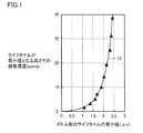
- FIG. 1 shows the measurement of the side lifetime of 10 silicon block samples, and then slicing the silicon block into a plurality of wafers and measuring the oxygen concentration of the wafer whose height was the minimum value. It is a graph obtained by plotting measurement data.
- the oxygen concentration was measured by an infrared absorption method using a Fourier transform infrared spectrometer (FT-IR).
- FT-IR Fourier transform infrared spectrometer
- the horizontal axis shows the minimum value of the lifetime in the bottom half of the silicon block
- the vertical axis shows the oxygen concentration at the height at which the lifetime becomes the minimum value.
- the lifetime is measured at a pitch of 2 mm at a position in the height direction at least on the bottom side in the lifetime measurement step.
- the oxygen concentration can also be measured by an inert gas melting method or SIMS (secondary ion mass spectrometry), but FIG. 1 shows the oxygen concentration measured by the infrared absorption method using FT-IR. The value of is used.
- the oxygen concentration value measured by FT-IR is a value measured by Nicolet 6700FT-IR manufactured by Thermo Fisher Scientific, 4 cm ⁇ 1 for wave number resolution, and 128 scans.
- the oxygen concentration at the height of the silicon block to be inspected can be derived from the minimum value of the lifetime of the bottom half of the silicon block by using the relationship shown by the curve 10 in FIG. .
- the reason why the lifetime data of minority carriers increases as the oxygen concentration increases is not necessarily clear.
- the lifetime killer iron This is thought to be because the impurity concentration in the silicon crystal is lowered by gettering (trapping) such as oxygen precipitation.
- Example of oxygen concentration calculation method at each position in the height direction In the silicon block cut out from the polycrystalline silicon ingot, the oxygen concentration attenuates in the height direction from the bottom portion to the top portion. Such attenuation follows a specific attenuation characteristic according to the manufacturing conditions of the polycrystalline silicon ingot. In carrying out the inspection method of the present invention, it is preferable that this attenuation characteristic is derived in advance.
- the attenuation characteristic of the oxygen concentration in the height direction depends on the manufacturing conditions of the polycrystalline silicon ingot, that is, the equipment and growth conditions used when manufacturing the polycrystalline silicon ingot.
- the damping characteristics may vary depending on the vacuum leak of the apparatus and the temperature at which the silicon raw material is melted. If the oxygen concentration at a certain height is calculated based on the attenuation characteristic of the oxygen concentration in the height direction derived in advance, the oxygen concentration at other heights can also be calculated. That is, the oxygen concentration in the entire silicon block can be calculated from the oxygen concentration at the reference position where the lifetime becomes the minimum value.
- the unused area determination step can be performed after the oxygen concentration calculation step.
- the lifetime of the side surface of the silicon block is measured to determine the minimum value of the lifetime on the bottom side, and the minimum value of the lifetime is shown in FIG.
- the oxygen concentration at the height is calculated by applying the relationship to the curve 10, and the height at which the oxygen concentration becomes a predetermined concentration is calculated by applying the oxygen concentration to the oxygen concentration attenuation characteristic in the height direction derived in advance. decide. For example, a region where the oxygen concentration is lower than a predetermined concentration can be used, and a region where the oxygen concentration is higher than a predetermined concentration can be used.
- the predetermined concentration can be appropriately determined according to the intended use of the silicon block, desired performance, and the like.
- the unused area of the silicon block determined in this way is preferably excised from the silicon block.
- the minimum value of the lifetime based on the measurement in the lifetime measurement step is a predetermined value or more, it is determined that the oxygen concentration is high in the oxygen concentration calculation step.
- the predetermined value of the lifetime can be set to 2 ⁇ s, for example.
- rough screening can be performed using the inspection method of the present invention.
- the silicon block of the present invention includes a step of preparing a silicon block, and a step of inspecting the silicon block by the above-described inspection method, and preferably cutting away the unused area determined in the unused area determining step. Manufactured by.
- the silicon wafer of the present invention includes a step of preparing a silicon block, and a step of inspecting the silicon block by the above-described inspection method, and preferably cutting away the unused area determined in the unused area determining step.
- the silicon block manufactured by the above method is used and sliced with a multi-wire saw or the like.
- a solar cell element After forming a pn junction using the silicon wafer of the present invention, a solar cell element is formed by attaching an antireflection film and an electrode. As described above, the solar cell element of the present invention is useful for reducing the cost because it can prepare and manufacture a silicon wafer that satisfies the specifications without incurring additional cost for the oxygen concentration test.
- a solar cell module is formed by electrically connecting a plurality of the solar cell elements of the present invention.
- the solar cell module of the present invention can be prepared and manufactured with a silicon wafer that satisfies the specifications without incurring additional costs for the oxygen concentration test, and thus is useful for reducing the cost.
- a silicon wafer is produced from a silicon block, and the oxygen concentration specification of the silicon wafer is less than 10 ppma.
- Example 1 A silicon block is cut out using a band saw from a silicon ingot formed by unidirectional solidification in the height direction from the bottom part to the top part, and two rectangular silicon blocks having a height of 20 cm (silicon block A, silicon block B). ) Prepared.
- the silicon block was inspected as follows according to the method of the present invention, and the region where the oxygen concentration was less than 10 ppma was used as the silicon block use region in accordance with the specifications of the silicon wafer to be produced.
- the relationship between the position in the height direction of the silicon block formed according to the manufacturing conditions of this example and the oxygen concentration is such that the position in the height direction of the bottom portion is 0 cm, and the position in the height direction is the distance from the bottom portion X (Cm), it was confirmed in advance using a plurality of silicon blocks having the same manufacturing conditions that the oxygen concentration Ox (ppma) at the position X (cm) in the height direction can be well fitted by the following equation (1). . Therefore, the relationship represented by the equation (1) is the oxygen concentration attenuation characteristic of the silicon block of this embodiment.
- Ox oxygen concentration in the bottom part / (X + 0.8) 0.7 formula (1)
- the relationship shown in Expression (1) reflects the property that the oxygen concentration attenuates in the height direction from the bottom portion to the top portion.
- the lifetimes of the height positions on the side surfaces were measured.
- a lifetime measuring device WT-2000 manufactured by Semilab was used. Measured by irradiating a laser beam at a laser wavelength of 904 nm, a pulse width of 200 ns, a laser spot of 1 mm 2 , a laser output of 1.2 ⁇ 10 13 (photons), a TimeRange of 0.1 ms, and a sensitivity of 100 mV. The average value of the measured values at the position of was taken as the lifetime at that height.
- the lifetime on the side surface of the silicon block was measured every 2 mm from the bottom position.
- 2A and 2B are graphs plotting the measurement results of the silicon blocks A and B, respectively.
- the horizontal axis represents the height of the silicon block
- the vertical axis represents the lifetime at each height.
- the horizontal axis indicates the height by the distance from the center, the center is 0, a higher position is indicated by plus, and a lower position is indicated by minus.
- the left side from the center is the bottom half of the silicon block
- the right side from the center is the top half of the silicon block.
- the minimum value excluding the measurement value at the bottom of the lifetime measurement values at the bottom half from the center of the silicon block is 1 at a position of 2 mm in height. 0.6 ⁇ s and 2.3 ⁇ s at a height of 17 mm.
- the oxygen concentration at the position where the lifetime becomes the minimum value of 1.6 ⁇ s is 5
- the oxygen concentration at the position where the lifetime was a minimum value of 2.3 ⁇ s was 25.3 ppma.
- the oxygen concentration in the bottom part with the highest oxygen concentration is 5.1 ppma, so that the oxygen concentration is less than 10 ppma in the entire region of the silicon block.
- the silicon block was sliced with a multi-wire saw to produce a silicon wafer satisfying the oxygen concentration specification.
- silicon block B 48.0 ppma, which is the oxygen concentration at the bottom, was substituted into equation (1) to determine the height of the silicon block at which the oxygen concentration was 10 ppma. It was calculated to be a position where the oxygen concentration was 10 ppma. As can be seen from the equation (1), the oxygen concentration is higher than 10 ppma at a position lower than this position. Therefore, a region having a height of 8.6 cm or less was excised and used for manufacturing a silicon wafer. A silicon wafer that satisfies the oxygen concentration specification was manufactured by slicing a silicon block that had been partially cut with a multi-wire saw. Table 1 summarizes the above results for block A and block B.
- Example 1 A silicon block is cut out using a band saw from a silicon ingot formed by unidirectional solidification in the height direction from the bottom portion to the top portion in the same manner as in Example 1, and a rectangular silicon block having a height of 20 cm (silicon Block C) was prepared.
- the silicon block was inspected as follows, and the region where the oxygen concentration was less than 10 ppma was used as the working region according to the specifications of the silicon wafer to be manufactured.
- the thickness of the thin piece is ideally about 2 mm. Therefore, in this comparative example, the thickness of the thin piece was cut to 2.5 mm with a band saw, the surface of the thin piece was polished, and then the thickness was reduced to 0. Etching was performed 5 mm to remove the damaged layer on the surface.
- the interstitial oxygen concentration was measured by FT-IR at a pitch of 5 mm in the same direction as the height direction of the silicon block C from the position corresponding to the bottom of the silicon block C. The oxygen concentration at the corresponding position of the flake was defined as the oxygen concentration in the height direction of the silicon block C.
- the oxygen concentration was 10 ppma or more at 25 mm from the bottom, and cutting was necessary. Therefore, a 25 mm region from the bottom of the silicon block C was cut out and used to manufacture a silicon wafer.
- a silicon wafer that satisfies the oxygen concentration specification was fabricated by slicing the silicon block, which had been partially cut, with a multi-wire saw.
- Example 2 A silicon block is cut out using a band saw from a silicon ingot formed by unidirectional solidification in the height direction from the bottom portion to the top portion in the same manner as in Example 1, and a rectangular silicon block having a height of 20 cm (silicon Block D) was prepared.
- the oxygen concentration is not inspected in the silicon block state, but the oxygen concentration is inspected after the silicon wafer is manufactured. The oxygen concentration is less than 10 ppma, and the oxygen concentration is 10 ppma or more. Were considered defective.
- the silicon wafer manufactured by the manufacturing method of this comparative example, or a solar cell and a solar cell module manufactured using the silicon wafer are manufactured using the silicon wafer manufactured by the manufacturing method of Example 1 or a solar cell manufactured using the silicon wafer. In comparison with the solar cell module, the cost is increased.
- the present invention since a silicon wafer that satisfies the specifications can be manufactured at low cost, the present invention can be suitably used in the solar cell field.
Landscapes
- Physics & Mathematics (AREA)
- Electromagnetism (AREA)
- Health & Medical Sciences (AREA)
- Life Sciences & Earth Sciences (AREA)
- Chemical & Material Sciences (AREA)
- Analytical Chemistry (AREA)
- Biochemistry (AREA)
- General Health & Medical Sciences (AREA)
- General Physics & Mathematics (AREA)
- Immunology (AREA)
- Pathology (AREA)
- Photovoltaic Devices (AREA)
- Testing Or Measuring Of Semiconductors Or The Like (AREA)
Abstract
本発明は、一方向凝固により形成された多結晶シリコンインゴットから切り出されたシリコンブロックの検査方法であって、シリコンブロックの少数キャリアのライフタイムを測定するライフタイム測定工程と、ライフタイム測定工程において測定したライフタイムからシリコンブロックの酸素濃度を算出する酸素濃度算出工程と、を含むシリコンブロックの検査方法を提供する。
Description
本発明は、シリコンブロックの検査方法、当該検査方法を経て製造されるシリコンブロックの製造方法およびシリコンブロック、当該検査方法を経て製造されるシリコンウェハの製造方法およびシリコンウェハ、当該シリコンウェハを用いて製造される太陽電池素子および太陽電池モジュールに関する。
環境問題から石油などの代替として自然エネルギーの利用が注目されている。太陽電池は大きな設備を必要とせず、稼働時に騒音などが出ないこともあり、日本や欧州などで特に積極的に導入されてきている。太陽電池の中ではカドミウムテルルなどの化合物半導体からなるものが登場してきたものの、物質自体の安全性やこれまでの実績、またコストパフォーマンスの面から、結晶系シリコンを基板として用いたシリコン太陽電池が大きなシェアを占めている。結晶系シリコンの基板は、さらに単結晶型、多結晶型に分類される。
シリコン太陽電池に用いられるシリコンの大部分は、坩堝内の溶融シリコンをボトム側から一方向に凝固させたシリコンインゴットを所定サイズのシリコンブロックに切り出し、そのブロックをマルチワイヤーソーなどの加工機で薄くスライスして得られたシリコンウェハが用いられている。このような方法で製造されたシリコンウェハは大部分が多結晶であるが、一部単結晶の種結晶を利用するなどして部分的に単結晶であるものなども製造されている。太陽電池には、B(ホウ素)をドーピングしたP型結晶シリコンウェハが広く使われている。
一方、J.Schmidt and A.Cuevas,J.Appl.Phys.86,3175(1999)(非特許文献1)に記載の通り、Bドープシリコンウェハを用いて作製された太陽電池では、光により太陽電池が劣化することが知られている。これは光照射により少数キャリアである電子のトラップとなるB-O対が生成されるためであると考えられる。そのため、光劣化率はB濃度、O(酸素)濃度の関数となっている。
したがって、結晶系シリコンウェハから製造した太陽電池の光劣化率を規定値以下に抑えるためにはウェハ中のB濃度、O濃度を評価する必要がある。B濃度はICP等の不純物分析や簡便な抵抗測定からも簡易評価可能であるが、酸素濃度は、スライスまで行った後にウェハの状態で測定を行うか、あるいはブロックに近い位置、あるいはブロックから薄板サンプル(約2mm厚程度が適当)を切り出し、研磨、エッチング処理等行った後にフーリエ変換赤外分光装置(FT-IR)などで評価する必要があった。
J.Schmidt and A.Cuevas,J.Appl.Phys.86,3175(1999)
しかしながら、上述のような酸素濃度測定では、以下のような問題が生じる。スライスまで行ないウェハ状態で酸素濃度を測定し、酸素濃度が規定値よりも高かった場合、スライスの加工費やカーフロスとなってしまったシリコン材料費など大きなコストアップ要因となる。また薄板サンプルを準備し評価する場合には、サンプル作製に手間がかかりやはりこの場合もコストアップ要因となる。
本発明は、上記問題点を回避するために行ったものであり、シリコンブロックの状態で、シリコン中の酸素濃度を簡便に評価することができるシリコンブロックの検査方法を提供することを目的とする。
本発明者は鋭意研究の結果、シリコンブロックの少数キャリアライフタイムのボトム側最小値とその高さ位置での酸素濃度との間に相関があることを見出し、本発明に至った。
本発明は、一方向凝固により形成された多結晶シリコンインゴットから切り出されたシリコンブロックの検査方法であって、シリコンブロックの少数キャリアのライフタイムを測定するライフタイム測定工程と、ライフタイム測定工程において測定したライフタイムからシリコンブロックの酸素濃度を算出する酸素濃度算出工程と、を含むシリコンブロックの検査方法を提供する。
本発明の検査方法の一実施形態においては、ライフタイム測定工程は、シリコンブロックの高さ方向の複数の位置で少数キャリアのライフタイムを測定する工程であり、酸素濃度算出工程は、高さ方向に二分したボトム側半分の位置で測定したライフタイムの内、最ボトム部を除いたライフタイムの最小値から、当該最小値をとる基準位置の酸素濃度を算出する工程を含む。
本発明の検査方法においては、多結晶シリコンインゴットの製造条件に応じて予め導き出された、シリコンブロックのボトム部からトップ部への高さ方向の酸素濃度の減衰特性と、酸素濃度算出工程で算出した基準位置の酸素濃度とを用いて、シリコンブロックの不使用領域を決定する不使用領域決定工程をさらに含むことが好ましい。
また本発明は、シリコンブロックを準備する工程と、上述のシリコンブロックの検査方法により当該シリコンブロックの検査を行ない、上記不使用領域決定工程で決定した不使用領域を切除する工程と、を含むシリコンブロックの製造方法およびかかる製造方法により製造されたシリコンブロックを提供する。
また本発明は、シリコンブロックを準備する工程と、上述のシリコンブロックの検査方法によりシリコンブロックの検査を行ない、上記不使用領域決定工程で決定した不使用領域を切除する工程と、上記不使用領域を切除したシリコンブロックをスライスしてシリコンウェハを作製する工程と、を含むシリコンウェハの製造方法およびかかる製造方法により製造されたシリコンウェハを提供する。
さらに本発明は、上述のシリコンウェハを備える太陽電池素子、およびかかる太陽電池素子の複数が電気的に接続されてなる太陽電池モジュールを提供する。
本発明のシリコンブロックの検査方法によると、簡易な方法で酸素濃度を算出することができ、酸素濃度が所定値以下であるシリコンブロックおよびシリコンウェハ、さらにはこのようなシリコンウェハからなる太陽電池素子および太陽電池モジュールを低コストで提供することができる。
[シリコンブロックの検査方法]
本発明のシリコンブロックの検査方法は、シリコンブロックの少数キャリアのライフタイムを測定するライフタイム測定工程と、ライフタイム測定工程において測定したライフタイムからシリコンブロックの酸素濃度を算出する酸素濃度算出工程と、を含む。本発明によると、酸素濃度を直接測定しなくても、ライフタイムの測定という簡便な方法により酸素濃度を算出することができる。
本発明のシリコンブロックの検査方法は、シリコンブロックの少数キャリアのライフタイムを測定するライフタイム測定工程と、ライフタイム測定工程において測定したライフタイムからシリコンブロックの酸素濃度を算出する酸素濃度算出工程と、を含む。本発明によると、酸素濃度を直接測定しなくても、ライフタイムの測定という簡便な方法により酸素濃度を算出することができる。
(シリコンブロックの形成工程)
シリコンブロックの形成工程の一形態を説明する。まず、溶融坩堝内にシリコン原料を投入し、加熱手段により溶融坩堝内のシリコン原料を溶融させ、その後、溶融坩堝内のシリコン原料がすべて溶融した後に、坩堝を傾けて溶融坩堝の上縁部にある注湯口から鋳型にシリコン融液を注湯する。注湯後は、鋳型内のシリコンをボトム部から冷却してボトム部からトップ部まで高さ方向に一方向凝固させた後、炉外に取り出せる温度まで温度制御しながら徐冷し、最終的に炉外に取り出す。このようにして、四角形型の多結晶シリコンインゴットを形成する。
シリコンブロックの形成工程の一形態を説明する。まず、溶融坩堝内にシリコン原料を投入し、加熱手段により溶融坩堝内のシリコン原料を溶融させ、その後、溶融坩堝内のシリコン原料がすべて溶融した後に、坩堝を傾けて溶融坩堝の上縁部にある注湯口から鋳型にシリコン融液を注湯する。注湯後は、鋳型内のシリコンをボトム部から冷却してボトム部からトップ部まで高さ方向に一方向凝固させた後、炉外に取り出せる温度まで温度制御しながら徐冷し、最終的に炉外に取り出す。このようにして、四角形型の多結晶シリコンインゴットを形成する。
そして、多結晶シリコンインゴットから、バンドソーなどを用いて、四角形型の多結晶シリコンブロックを切り出す。切り出したシリコンブロックに対して、必要に応じて、寸法出し、エッチングなどの仕上げ工程を行なってもよい。
(ライフタイム測定工程)
本明細書では、μPCD法(マイクロ波光導電率減衰法)による少数キャリアのライフタイムを用いた例を示すが、他の方法も使用可能である。本明細書におけるライフタイムの測定方法は、シリコンブロックの側面の高さ方向における複数の位置で、Semilab社製ライフタイム測定装置WT-2000を用いて測定を行なう。レーザー波長904nm、パルス幅200ns、レーザースポット1mm2、レーザー出力1.2×10¹³(photons)、TimeRange0.1ms、Sensitivity100mVでレーザー光を照射して測定する。測定するラインは1ラインでもよいが、より精度を上げるためには、シリコンブロックを幅方向に所定間隔でスキャンし、同一の高さの位置における複数の測定値の平均値をその高さにおけるライフタイムとする。スキャンを行なう所定間隔および測定値の数はシリコンブロックのサイズに応じて適宜決定することができる。たとえば、幅が156mmのシリコンブロックに対して、幅方向に20mm間隔でスキャンを行ない8ラインで測定し、ある高さでの8ラインでの測定値の平均値をその高さにおけるライフタイムとすることができる。各ラインにおける高さ方向のライフタイムの測定間隔は限定されないが、たとえば2mm間隔とすることができる。
本明細書では、μPCD法(マイクロ波光導電率減衰法)による少数キャリアのライフタイムを用いた例を示すが、他の方法も使用可能である。本明細書におけるライフタイムの測定方法は、シリコンブロックの側面の高さ方向における複数の位置で、Semilab社製ライフタイム測定装置WT-2000を用いて測定を行なう。レーザー波長904nm、パルス幅200ns、レーザースポット1mm2、レーザー出力1.2×10¹³(photons)、TimeRange0.1ms、Sensitivity100mVでレーザー光を照射して測定する。測定するラインは1ラインでもよいが、より精度を上げるためには、シリコンブロックを幅方向に所定間隔でスキャンし、同一の高さの位置における複数の測定値の平均値をその高さにおけるライフタイムとする。スキャンを行なう所定間隔および測定値の数はシリコンブロックのサイズに応じて適宜決定することができる。たとえば、幅が156mmのシリコンブロックに対して、幅方向に20mm間隔でスキャンを行ない8ラインで測定し、ある高さでの8ラインでの測定値の平均値をその高さにおけるライフタイムとすることができる。各ラインにおける高さ方向のライフタイムの測定間隔は限定されないが、たとえば2mm間隔とすることができる。
なお、ライフタイムの測定に関しては、標準サンプルは存在しないため較正は各装置ごとに異なる。したがって、図1のグラフの縦軸は較正によって異なるため、予め各装置ごとに作成しておく必要がある。
(酸素濃度算出工程)
シリコンブロックのライフタイムと、酸素濃度との関係に基づき、ライフタイム測定工程で測定したライフタイムから、シリコンブロックの酸素濃度を算出する。シリコンブロックの酸素濃度は、各高さの位置での酸素濃度が算出されることが好ましい。算出されたシリコンブロックの酸素濃度は、シリコンブロックを評価する上で有用である。たとえば、シリコンブロックをスライスしてシリコンウェハを作製するに際して、算出した酸素濃度に基づいて酸素濃度が所定の範囲内である領域を選択し、使用領域とすることにより、酸素濃度を直接測定しなくても酸素濃度が所定の範囲内であるシリコンウェハを作製することができる。以下、ライフタイムと酸素濃度の関係の一例、およびその関係を用いて行なう不使用領域決定工程について説明する。
シリコンブロックのライフタイムと、酸素濃度との関係に基づき、ライフタイム測定工程で測定したライフタイムから、シリコンブロックの酸素濃度を算出する。シリコンブロックの酸素濃度は、各高さの位置での酸素濃度が算出されることが好ましい。算出されたシリコンブロックの酸素濃度は、シリコンブロックを評価する上で有用である。たとえば、シリコンブロックをスライスしてシリコンウェハを作製するに際して、算出した酸素濃度に基づいて酸素濃度が所定の範囲内である領域を選択し、使用領域とすることにより、酸素濃度を直接測定しなくても酸素濃度が所定の範囲内であるシリコンウェハを作製することができる。以下、ライフタイムと酸素濃度の関係の一例、およびその関係を用いて行なう不使用領域決定工程について説明する。
<ライフタイムと酸素濃度の関係の一例>
シリコンブロックの側面の複数の高さの位置で測定したライフタイムであって、シリコンブロックを高さ方向に二分したボトム側半分のライフタイムの測定値の内、高さ0の位置(最ボトム部)の測定値を除く最小値(以下、単に「ボトム側のライフタイムの最小値」ともいう)と、ライフタイムがかかる最小値となる高さ(本明細書においては「基準位置」ともいう)での酸素濃度との間に、図1の曲線10に示すような正の相関関係があることが見出された。なお、シリコンブロックにおいて、「高さ方向」は一方向凝固における凝固方向と一致する方向であり、「最ボトム部」は高さ方向において一方向凝固の起点の最も近くに位置する。
シリコンブロックの側面の複数の高さの位置で測定したライフタイムであって、シリコンブロックを高さ方向に二分したボトム側半分のライフタイムの測定値の内、高さ0の位置(最ボトム部)の測定値を除く最小値(以下、単に「ボトム側のライフタイムの最小値」ともいう)と、ライフタイムがかかる最小値となる高さ(本明細書においては「基準位置」ともいう)での酸素濃度との間に、図1の曲線10に示すような正の相関関係があることが見出された。なお、シリコンブロックにおいて、「高さ方向」は一方向凝固における凝固方向と一致する方向であり、「最ボトム部」は高さ方向において一方向凝固の起点の最も近くに位置する。
図1は、10個のシリコンブロックのサンプルについて側面のライフタイムを測定し、その後シリコンブロックをスライスして複数枚のウェハとし、ライフタイムが最小値であった高さのウェハの酸素濃度を測定し、測定データをプロットして得たグラフである。酸素濃度の測定は、フーリエ変換赤外分光装置(FT-IR)による赤外吸収法で行なった。
図1においては、横軸はシリコンブロックのボトム側半分におけるライフタイムの最小値を示し、縦軸はライフタイムが最小値となる高さでの酸素濃度を示す。なお、ボトム側半分のライフタイムの最小値を求めるためには、ライフタイム測定工程において、少なくともボトム側においては、高さ方向の位置において2mmのピッチでライフタイムが測定されることが好ましい。ボトム側半分のライフタイムの最小値を決定するに際して、最ボトム部の測定値を除いた理由としては、ライフタイムの試料端部でのデータが、入射ビームの当たり方の少しの変動に敏感で不安定になる傾向があるためである。
酸素濃度の測定方法としては、その他、不活性ガス溶融法やSIMS(二次イオン質量分析法)などで測定することもできるが、図1はFT-IRによる赤外吸収法で測定した酸素濃度の値を用いる。本明細書において、FT-IRで測定した酸素濃度値は、サーモフィッシャーサイエンティフィック社製Nicolet6700FT-IR、波数分解用4cm-1、スキャン回数128回で測定を行なった値である。
以上より、検査対象のシリコンブロックについて、シリコンブロックのボトム側半分のライフタイムの最小値から、図1の曲線10に示す関係を用いることにより、その高さでの酸素濃度が導き出されることがわかる。
なお、図1に示すように、酸素濃度が高いほど少数キャリアのライフタイムデータが高くなる理由は必ずしも明らかではないが、通常ボトム側の坩堝から凝固後に固相拡散してくるライフタイムキラー(鉄などの重金属)が、酸素析出などにゲッタリング(捕捉)されることで、シリコン結晶内部の不純物濃度が下がるためであると考えられる。
<高さ方向の各位置での酸素濃度の算出方法の一例>
多結晶シリコンインゴットから切り出されたシリコンブロックにおいて、酸素濃度は、ボトム部からトップ部の高さ方向に減衰する。かかる減衰は、多結晶シリコンインゴットの製造条件に応じた特定の減衰特性にしたがうものである。本発明の検査方法を実施するに際して、この減衰特性が予め導き出されていることが好ましい。
多結晶シリコンインゴットから切り出されたシリコンブロックにおいて、酸素濃度は、ボトム部からトップ部の高さ方向に減衰する。かかる減衰は、多結晶シリコンインゴットの製造条件に応じた特定の減衰特性にしたがうものである。本発明の検査方法を実施するに際して、この減衰特性が予め導き出されていることが好ましい。
高さ方向の酸素濃度の減衰特性は、多結晶シリコンインゴットの製造条件、すなわち多結晶シリコンインゴットを製造する際に用いる装置や成長条件などに依存する。装置の真空系リークや、シリコン原料溶融時の温度などによっても減衰特性が異なる場合がある。予め導き出された高さ方向の酸素濃度の減衰特性に基づくと、ある高さでの酸素濃度が算出されれば、他の高さでの酸素濃度も算出することができる。すなわち、ライフタイムが最小値となる基準位置での酸素濃度からシリコンブロック全域の酸素濃度を算出することができる。
(不使用領域決定工程)
本発明の検査方法においては、酸素濃度算出工程の後、不使用領域決定工程を行なうことができる。不使用領域決定工程を行なう場合、本発明の一実施形態においては、シリコンブロックの側面のライフタイムを測定してボトム側のライフタイムの最小値を決定し、ライフタイムの最小値を図1の曲線10に関係に当てはめてその高さでの酸素濃度を算出し、かかる酸素濃度を予め導き出された高さ方向の酸素濃度の減衰特性に当てはめて、酸素濃度が所定の濃度となる高さを決定する。そして、たとえば、酸素濃度が所定の濃度未満の領域を使用領域とし、所定の濃度以上の領域を不使用領域とすることができる。所定の濃度は、シリコンブロックの使用用途、所望の性能等に応じて適宜決定することができる。このように決定されたシリコンブロックの不使用領域は、好ましくはシリコンブロックから切除する。
本発明の検査方法においては、酸素濃度算出工程の後、不使用領域決定工程を行なうことができる。不使用領域決定工程を行なう場合、本発明の一実施形態においては、シリコンブロックの側面のライフタイムを測定してボトム側のライフタイムの最小値を決定し、ライフタイムの最小値を図1の曲線10に関係に当てはめてその高さでの酸素濃度を算出し、かかる酸素濃度を予め導き出された高さ方向の酸素濃度の減衰特性に当てはめて、酸素濃度が所定の濃度となる高さを決定する。そして、たとえば、酸素濃度が所定の濃度未満の領域を使用領域とし、所定の濃度以上の領域を不使用領域とすることができる。所定の濃度は、シリコンブロックの使用用途、所望の性能等に応じて適宜決定することができる。このように決定されたシリコンブロックの不使用領域は、好ましくはシリコンブロックから切除する。
本発明の検査方法の他の実施形態として、ライフタイム測定工程での測定に基づくライフタイムの最小値が所定の値以上である場合には、酸素濃度算出工程において酸素濃度が高いと判断し、酸素濃度が高いと判断されたシリコンブロックについてのみ詳細な評価を行なうようにする実施形態が挙げられる。ここでのライフタイムの所定の値は、たとえば2μsとすることができる。この実施形態においては、本発明の検査方法を用いて、大雑把なスクリーニングを行なうことができる。
[シリコンブロック]
本発明のシリコンブロックは、シリコンブロックを準備する工程と、上述の検査方法によりシリコンブロックの検査を行ない、好ましくは不使用領域決定工程において決定された不使用領域を切除する工程と、を含む方法により製造される。
本発明のシリコンブロックは、シリコンブロックを準備する工程と、上述の検査方法によりシリコンブロックの検査を行ない、好ましくは不使用領域決定工程において決定された不使用領域を切除する工程と、を含む方法により製造される。
このような製造方法により、酸素濃度を直接測定することなく、酸素濃度が所定の濃度未満の領域のみからなるシリコンブロックを調整することができる。したがって、酸素濃度を直接測定する場合に必要なコストをかける必要がないため、シリコンブロックおよびこれをスライスして作製するシリコンウェハの低価格化に有用である。
[シリコンウェハ]
本発明のシリコンウェハは、シリコンブロックを準備する工程と、上述の検査方法によりシリコンブロックの検査を行ない、好ましくは不使用領域決定工程において決定された不使用領域を切除する工程と、を含む方法により製造されたシリコンブロックを用い、これをマルチワイヤソーなどでスライスして作製する。
本発明のシリコンウェハは、シリコンブロックを準備する工程と、上述の検査方法によりシリコンブロックの検査を行ない、好ましくは不使用領域決定工程において決定された不使用領域を切除する工程と、を含む方法により製造されたシリコンブロックを用い、これをマルチワイヤソーなどでスライスして作製する。
[太陽電池素子]
本発明のシリコンウェハを使用してp-n接合を形成した後、反射防止膜、電極を取り付けることで太陽電池素子が形成される。本発明の太陽電池素子は、上述したように、酸素濃度検査に追加のコストをかけることになく仕様を満たしたシリコンウェハを準備して製造することができるので、低価格化に有用である。
本発明のシリコンウェハを使用してp-n接合を形成した後、反射防止膜、電極を取り付けることで太陽電池素子が形成される。本発明の太陽電池素子は、上述したように、酸素濃度検査に追加のコストをかけることになく仕様を満たしたシリコンウェハを準備して製造することができるので、低価格化に有用である。
[太陽電池モジュール]
本発明の太陽電池素子の複数を電気的に接続することにより、太陽電池モジュールが形成される。本発明の太陽電池モジュールは、上述したように、酸素濃度検査に追加のコストをかけることなく仕様を満たしたシリコンウェハを準備して製造することができるので、低価格化に有用である。
本発明の太陽電池素子の複数を電気的に接続することにより、太陽電池モジュールが形成される。本発明の太陽電池モジュールは、上述したように、酸素濃度検査に追加のコストをかけることなく仕様を満たしたシリコンウェハを準備して製造することができるので、低価格化に有用である。
以下、実施例を挙げて本発明をさらに詳しく説明するが、本発明はこれら実施例に限定されるものではない。以下の実施例、比較例においては、シリコンブロックからシリコンウェハを作製するが、シリコンウェハの酸素濃度の仕様は10ppma未満とする。
[実施例1]
ボトム部からトップ部への高さ方向の一方向凝固により形成したシリコンインゴットから、バンドソーを用いてシリコンブロックを切り出し、高さ20cmの四角形型のシリコンブロックを二つ(シリコンブロックA,シリコンブロックB)用意した。本実施例では、本発明の方法にしたがって以下のようにシリコンブロックの検査を行ない、作製するシリコンウェハの仕様に合わせて、酸素濃度が10ppma未満の領域をシリコンブロックの使用領域とした。
ボトム部からトップ部への高さ方向の一方向凝固により形成したシリコンインゴットから、バンドソーを用いてシリコンブロックを切り出し、高さ20cmの四角形型のシリコンブロックを二つ(シリコンブロックA,シリコンブロックB)用意した。本実施例では、本発明の方法にしたがって以下のようにシリコンブロックの検査を行ない、作製するシリコンウェハの仕様に合わせて、酸素濃度が10ppma未満の領域をシリコンブロックの使用領域とした。
本実施例の製造条件により形成されたシリコンブロックの高さ方向の位置と酸素濃度の関係は、ボトム部の高さ方向の位置を0cmとし、高さ方向の位置をボトム部からの距離でX(cm)とすると、高さ方向の位置X(cm)での酸素濃度Ox(ppma)は、以下の式(1)でよくフィッティングできることを、同一製造条件のシリコンブロックを複数用いて予め確認した。したがって、式(1)に示される関係を、本実施例のシリコンブロックの酸素濃度の減衰特性とする。
Ox=最ボトム部の酸素濃度/(X+0.8)0.7 式(1)
式(1)に示す関係には、ボトム部からトップ部の高さ方向に酸素濃度が減衰する性質が反映されている。
式(1)に示す関係には、ボトム部からトップ部の高さ方向に酸素濃度が減衰する性質が反映されている。
シリコンブロックA,Bについて、その側面の複数の高さの位置のライフタイムを測定した。測定には、Semilab社製ライフタイム測定装置WT-2000を用いた。レーザー波長904nm、パルス幅200ns、レーザースポット1mm2、レーザー出力1.2×10¹³(photons)、TimeRange0.1ms、Sensitivity100mVでレーザー光を照射して測定し、シリコンブロックの8ラインの同一の高さの位置における測定値の平均値をその高さにおけるライフタイムとした。シリコンブロックの側面におけるライフタイムは、最ボトムの位置から2mm毎に測定した。
図2(A)および図2(B)は、それぞれシリコンブロックA,Bの測定結果をプロットしたグラフである。図2(A)および図2(B)中、横軸はシリコンブロックの高さを表し、縦軸は各高さでのライフタイムを表している。なお、横軸は、中心からの距離で高さを示し、中心を0として、それより高い位置をプラスで、それより低い位置をマイナスで示す。すなわち、図2(A)および図2(B)の横軸において、中心より左側はシリコンブロックのボトム側半分であり、中心より右側はシリコンブロックのトップ側半分である。
シリコンブロックA,Bのライフタイムの測定結果から、シリコンブロックの中心よりボトム側半分のライフタイムの測定値の内、最ボトム部の測定値を除く最小値は、それぞれ高さ2mmの位置の1.6μsと、高さ17mmの位置の2.3μsであった。このボトム側半分のライフタイムの最小値から、図1に示す曲線10の関係に基づきその高さの酸素濃度を求めたところ、ライフタイムが最小値1.6μsとなる位置での酸素濃度は5.1ppmaであり、ライフタイムが最小値2.3μsとなる位置での酸素濃度は25.3ppmaであった。そして、ライフタイム最小値をとる高さ方向の位置(X)と、その位置での酸素濃度Oxを式(1)に代入して最ボトム部の酸素濃度を算出したところ、シリコンブロックA,Bにおいてそれぞれ5.1ppma(=5.1ppma×(0.2+0.8)0.7)と48.0ppma(=25.3ppma×(1.7+0.8)0.7)であった。シリコンブロックAでは、最も酸素濃度が高い最ボトム部の酸素濃度が5.1ppmaであるのでシリコンブロックの全領域において酸素濃度は10ppma未満であり、切除せずにそのままシリコンウェハの作製に用いた。シリコンブロックをマルチワイヤソーでスライス加工し、酸素濃度の仕様を満たすシリコンウェハを作製した。
シリコンブロックBについて、最ボトム部の酸素濃度である48.0ppmaを式(1)に代入して、酸素濃度が10ppmaとなるシリコンブロックの高さを求めたところ、高さ8.6cmの位置が酸素濃度10ppmaになる位置であると算出された。式(1)からわかるように、この位置より高さが低い位置は酸素濃度が10ppmaより高くなるので、高さ8.6cm以下の領域を切除して、シリコンウェハの作製に用いた。一部を切除したシリコンブロックをマルチワイヤソーでスライス加工し、酸素濃度の仕様を満たすシリコンウェハを作製した。表1は、ブロックAおよびブロックBの上述の結果をまとめたものである。

[比較例1]
実施例1と同様の方法により、ボトム部からトップ部への高さ方向の一方向凝固により形成したシリコンインゴットから、バンドソーを用いてシリコンブロックを切り出し、高さ20cmの四角形型のシリコンブロック(シリコンブロックC)を用意した。本比較例では、以下のようにシリコンブロックの検査を行ない、作製するシリコンウェハの仕様に合わせて、酸素濃度が10ppma未満の領域を使用領域とした。
実施例1と同様の方法により、ボトム部からトップ部への高さ方向の一方向凝固により形成したシリコンインゴットから、バンドソーを用いてシリコンブロックを切り出し、高さ20cmの四角形型のシリコンブロック(シリコンブロックC)を用意した。本比較例では、以下のようにシリコンブロックの検査を行ない、作製するシリコンウェハの仕様に合わせて、酸素濃度が10ppma未満の領域を使用領域とした。
本比較例では、シリコンブロックCを切り出した際に、シリコンインゴットのシリコンブロックCに隣接した位置から結晶成長方向に平行な酸素濃度測定用の薄片を切り出した。酸素濃度を測定する上で、薄片の厚さは2mm程度が理想的であるため、本比較例ではバンドソーで厚さ2.5mmに切断し、薄片の表面を研磨後、フッ硝酸にて0.5mmエッチングし、表面のダメージ層を除去した。このように処理した薄片について、シリコンブロックCの最ボトム部に対応する位置からシリコンブロックCの高さ方向と同じ方向に5mmピッチでFT-IRによって格子間酸素濃度を測定した。薄片の対応する位置の酸素濃度をシリコンブロックCの高さ方向の酸素濃度とした。
この測定の結果、最ボトム部から25mmでは酸素濃度が10ppma以上であり、切断が必要であることが分かった。したがって、シリコンブロックCの最ボトム部から25mmの領域を切除して、シリコンウェハの作製に用いた。一部を切除したシリコンブロックをマルチワイヤーソーでスライス加工し、酸素濃度の仕様を満たすシリコンウェハを作製した。
本比較例では、厚さ2.5mmの酸素濃度測定用の薄片を切り出すために、カーフロス約3mmのバンドソーにて加工を行なったため、薄片側と薄片が切り出されたシリコンインゴット側の厚さ合計6mmのシリコンがくずとなった。またその他に、バンドソー加工、薄片の研磨・エッチング加工、FT-IRの測定など手間・費用が発生した。したがって本比較例の製造方法により製造されるシリコンウェハ、またはこれを用いて作製する太陽電池、太陽電池モジュールは、実施例1の製造方法により製造されるシリコンウェハまたはこれを用いて作製する太陽電池、太陽電池モジュールと比較してコストアップとなる。
[比較例2]
実施例1と同様の方法により、ボトム部からトップ部への高さ方向の一方向凝固により形成したシリコンインゴットから、バンドソーを用いてシリコンブロックを切り出し、高さ20cmの四角形型のシリコンブロック(シリコンブロックD)を用意した。本比較例では、シリコンブロックの状態での酸素濃度の検査は行なわずに、シリコンウェハを作製してから酸素濃度の検査を行ない、酸素濃度が10ppma未満のものを良品とし、酸素濃度が10ppma以上のものを不良品とした。
実施例1と同様の方法により、ボトム部からトップ部への高さ方向の一方向凝固により形成したシリコンインゴットから、バンドソーを用いてシリコンブロックを切り出し、高さ20cmの四角形型のシリコンブロック(シリコンブロックD)を用意した。本比較例では、シリコンブロックの状態での酸素濃度の検査は行なわずに、シリコンウェハを作製してから酸素濃度の検査を行ない、酸素濃度が10ppma未満のものを良品とし、酸素濃度が10ppma以上のものを不良品とした。
シリコンブロックDをマルチワイヤソーでスライス加工し、ブロック最ボトム部に対応するシリコンウェハから15枚おきにFT-IR測定を行なった結果、最ボトムから90枚が酸素濃度の仕様を満たしていないことが分かった。そこで、該当の90枚を不良品として抜き取り、残りを酸素濃度の仕様を満たしているシリコンウェハとした。
本比較例では、最終的に不良品として処理される最ボトム部分から90枚をウェハ化するためのスライス処理、不良品として処理される90枚のウェハのスライス時に発生したシリコンくずの処理およびFT-IR測定処理の手間と費用、その他(90枚分の生産減分の固定費アップなど)の費用などがかかった。したがって本比較例の製造方法により製造されるシリコンウェハ、またはこれを用いて作製する太陽電池、太陽電池モジュールは、実施例1の製造方法により製造されるシリコンウェハまたはこれを用いて作製する太陽電池、太陽電池モジュールと比較してコストアップとなる。
本発明によれば、低コストで仕様を満たすシリコンウェハを製造することができるので、本発明は太陽電池分野に好適に利用することができる。
Claims (9)
- 一方向凝固により形成された多結晶シリコンインゴットから切り出されたシリコンブロックの検査方法であって、
前記シリコンブロックの少数キャリアのライフタイムを測定するライフタイム測定工程と、
前記ライフタイム測定工程において測定した前記ライフタイムから前記シリコンブロックの酸素濃度を算出する酸素濃度算出工程と、を含むシリコンブロックの検査方法。 - 前記ライフタイム測定工程は、前記シリコンブロックの高さ方向の複数の位置で少数キャリアのライフタイムを測定する工程であり、
前記酸素濃度算出工程は、前記高さ方向で二分したボトム側半分の位置で測定したライフタイムの内、最ボトム部を除いたライフタイムの最小値から、前記最小値をとる基準位置の酸素濃度を算出する工程を含む、請求項1に記載のシリコンブロックの検査方法。 - 前記多結晶シリコンインゴットの製造条件に応じて予め導き出された、前記シリコンブロックのボトム部からトップ部への高さ方向の酸素濃度の減衰特性と、前記酸素濃度算出工程で算出した前記基準位置の前記酸素濃度とを用いて、前記シリコンブロックの不使用領域を決定する不使用領域決定工程をさらに含む、請求項2に記載のシリコンブロックの検査方法。
- シリコンブロックを準備する工程と、
請求項3に記載のシリコンブロックの検査方法により前記シリコンブロックの検査を行ない、前記不使用領域を切除する工程と、を含むシリコンブロックの製造方法。 - 請求項4に記載の製造方法により製造されたシリコンブロック。
- シリコンブロックを準備する工程と、
請求項3に記載のシリコンブロックの検査方法により前記シリコンブロックの検査を行ない、前記不使用領域を切除する工程と、
前記不使用領域を切除した前記シリコンブロックをスライスしてシリコンウェハを作製する工程と、を含むシリコンウェハの製造方法。 - 請求項6に記載のシリコンウェハの製造方法により製造された、シリコンウェハ。
- 請求項7に記載のシリコンウェハを備える、太陽電池素子。
- 請求項8に記載の太陽電池素子の複数が電気的に接続されてなる、太陽電池モジュール。
Applications Claiming Priority (2)
| Application Number | Priority Date | Filing Date | Title |
|---|---|---|---|
| JP2011229529A JP5367796B2 (ja) | 2011-10-19 | 2011-10-19 | シリコンブロックの検査方法および製造方法、シリコンウェハの製造方法、太陽電池素子の製造方法ならびに太陽電池モジュールの製造方法 |
| JP2011-229529 | 2011-10-19 |
Publications (1)
| Publication Number | Publication Date |
|---|---|
| WO2013058036A1 true WO2013058036A1 (ja) | 2013-04-25 |
Family
ID=48140692
Family Applications (1)
| Application Number | Title | Priority Date | Filing Date |
|---|---|---|---|
| PCT/JP2012/073282 Ceased WO2013058036A1 (ja) | 2011-10-19 | 2012-09-12 | シリコンブロックの検査方法および製造方法、シリコンブロック、シリコンウェハの製造方法、シリコンウェハ、太陽電池素子ならびに太陽電池モジュール |
Country Status (2)
| Country | Link |
|---|---|
| JP (1) | JP5367796B2 (ja) |
| WO (1) | WO2013058036A1 (ja) |
Cited By (1)
| Publication number | Priority date | Publication date | Assignee | Title |
|---|---|---|---|---|
| CN117085967A (zh) * | 2023-09-01 | 2023-11-21 | 四川晶科能源有限公司 | 一种硅料分类方法 |
Citations (1)
| Publication number | Priority date | Publication date | Assignee | Title |
|---|---|---|---|---|
| JP2011138866A (ja) * | 2009-12-28 | 2011-07-14 | Mitsubishi Materials Corp | 多結晶シリコンブロック材の製造方法、多結晶シリコンウエハの製造方法及び多結晶シリコンブロック材 |
-
2011
- 2011-10-19 JP JP2011229529A patent/JP5367796B2/ja not_active Expired - Fee Related
-
2012
- 2012-09-12 WO PCT/JP2012/073282 patent/WO2013058036A1/ja not_active Ceased
Patent Citations (1)
| Publication number | Priority date | Publication date | Assignee | Title |
|---|---|---|---|---|
| JP2011138866A (ja) * | 2009-12-28 | 2011-07-14 | Mitsubishi Materials Corp | 多結晶シリコンブロック材の製造方法、多結晶シリコンウエハの製造方法及び多結晶シリコンブロック材 |
Non-Patent Citations (2)
| Title |
|---|
| FUTOSHI KUSUOKA: "Ga Dope Oyobi B Dope Takessho Silicon Ingot no Tokusei Hyoka", EXTENDED ABSTRACTS (THE 54TH SPRING MEETING, 2007); THE JAPAN SOCIETY OF APPLIED PHYSICS AND RELATED SOCIETIES NO.3, THE JAPAN SOCIETY OF APPLIED PHYSICS, no. 3, 2007 * |
| GATOS H. C. ET AL.: "Microdistribution of oxygen in silicon and its effects on electronic properties", NASA CONF PUBL, 1982, pages 163 - 169 * |
Cited By (1)
| Publication number | Priority date | Publication date | Assignee | Title |
|---|---|---|---|---|
| CN117085967A (zh) * | 2023-09-01 | 2023-11-21 | 四川晶科能源有限公司 | 一种硅料分类方法 |
Also Published As
| Publication number | Publication date |
|---|---|
| JP5367796B2 (ja) | 2013-12-11 |
| JP2013089794A (ja) | 2013-05-13 |
Similar Documents
| Publication | Publication Date | Title |
|---|---|---|
| TWI609177B (zh) | 晶圓成像及處理方法與裝置 | |
| WO2012027788A1 (en) | Systems and methods for detecting crystal defects in monocrystalline semiconductors | |
| Michl et al. | The impact of different diffusion temperature profiles on iron concentrations and carrier lifetimes in multicrystalline silicon wafers | |
| JP5630665B2 (ja) | 結晶シリコンインゴット及びその製造方法 | |
| Nguyen et al. | Microscopic distributions of defect luminescence from subgrain boundaries in multicrystalline silicon wafers | |
| Huster et al. | ECV doping profile measurements of aluminium alloyed back surface fields | |
| JP5367796B2 (ja) | シリコンブロックの検査方法および製造方法、シリコンウェハの製造方法、太陽電池素子の製造方法ならびに太陽電池モジュールの製造方法 | |
| JP6734150B2 (ja) | 多結晶シリコン柱 | |
| Sinton et al. | Evaluating silicon blocks and ingots with quasi-steady-state lifetime measurements | |
| CN203705326U (zh) | 承载碲锌镉样品的装置 | |
| CN103828064B (zh) | 太阳能电池用晶片、太阳能电池用晶片的生产方法、太阳能电池的生产方法和太阳能电池模块的生产方法 | |
| JP5885195B2 (ja) | Si結晶の結晶品質評価方法及び結晶品質評価装置 | |
| TWI641825B (zh) | GaAs crystal | |
| TW202120751A (zh) | 具有低氧濃度區之晶圓 | |
| CN103674841B (zh) | 承载碲锌镉样品的装置和测试碲锌镉中Zn组分的方法 | |
| Nosho et al. | Lateral uniformity in HgCdTe layers grown by molecular beam epitaxy | |
| Agaiby et al. | Stress and doping uniformity of laser crystallized amorphous silicon in thin film silicon solar cells | |
| Pavelka et al. | Carrier lifetime measurements in silicon for photovoltaic applications | |
| Oliveira et al. | Recombination activity of 2D extended defects in monolike silicon | |
| Berthod et al. | Experimental investigation of the optimal ingot resistivity for both the cell performances and the temperature coefficients for different cell architectures | |
| KR20210059739A (ko) | 반도체 샘플의 열 도너 농도를 결정하는 방법 | |
| JP2002148191A (ja) | 半導体の特性評価方法およびその装置 | |
| KR101502389B1 (ko) | 태양전지 광흡수층의 정량분석법 | |
| Chung et al. | Photoluminescence imaging for quality control in silicon solar cell manufacturing | |
| Hess et al. | Impact of the crystal structure on solar cell parameters of Ribbon Growth on Substrate (RGS) solar cells |
Legal Events
| Date | Code | Title | Description |
|---|---|---|---|
| 121 | Ep: the epo has been informed by wipo that ep was designated in this application |
Ref document number: 12841290 Country of ref document: EP Kind code of ref document: A1 |
|
| NENP | Non-entry into the national phase |
Ref country code: DE |
|
| 122 | Ep: pct application non-entry in european phase |
Ref document number: 12841290 Country of ref document: EP Kind code of ref document: A1 |