WO2013054487A1 - 色素増感型光電気化学セル用半導体光電極およびその製造方法ならびに色素増感型光電気化学セル - Google Patents
色素増感型光電気化学セル用半導体光電極およびその製造方法ならびに色素増感型光電気化学セル Download PDFInfo
- Publication number
- WO2013054487A1 WO2013054487A1 PCT/JP2012/006320 JP2012006320W WO2013054487A1 WO 2013054487 A1 WO2013054487 A1 WO 2013054487A1 JP 2012006320 W JP2012006320 W JP 2012006320W WO 2013054487 A1 WO2013054487 A1 WO 2013054487A1
- Authority
- WO
- WIPO (PCT)
- Prior art keywords
- dye
- porous
- photoelectrochemical cell
- semiconductor
- current collector
- Prior art date
- Legal status (The legal status is an assumption and is not a legal conclusion. Google has not performed a legal analysis and makes no representation as to the accuracy of the status listed.)
- Ceased
Links
Images


Classifications
-
- H—ELECTRICITY
- H01—ELECTRIC ELEMENTS
- H01G—CAPACITORS; CAPACITORS, RECTIFIERS, DETECTORS, SWITCHING DEVICES, LIGHT-SENSITIVE OR TEMPERATURE-SENSITIVE DEVICES OF THE ELECTROLYTIC TYPE
- H01G9/00—Electrolytic capacitors, rectifiers, detectors, switching devices, light-sensitive or temperature-sensitive devices; Processes of their manufacture
- H01G9/20—Light-sensitive devices
- H01G9/2027—Light-sensitive devices comprising an oxide semiconductor electrode
- H01G9/2031—Light-sensitive devices comprising an oxide semiconductor electrode comprising titanium oxide, e.g. TiO2
-
- H—ELECTRICITY
- H01—ELECTRIC ELEMENTS
- H01G—CAPACITORS; CAPACITORS, RECTIFIERS, DETECTORS, SWITCHING DEVICES, LIGHT-SENSITIVE OR TEMPERATURE-SENSITIVE DEVICES OF THE ELECTROLYTIC TYPE
- H01G9/00—Electrolytic capacitors, rectifiers, detectors, switching devices, light-sensitive or temperature-sensitive devices; Processes of their manufacture
- H01G9/20—Light-sensitive devices
- H01G9/2068—Panels or arrays of photoelectrochemical cells, e.g. photovoltaic modules based on photoelectrochemical cells
-
- H—ELECTRICITY
- H01—ELECTRIC ELEMENTS
- H01G—CAPACITORS; CAPACITORS, RECTIFIERS, DETECTORS, SWITCHING DEVICES, LIGHT-SENSITIVE OR TEMPERATURE-SENSITIVE DEVICES OF THE ELECTROLYTIC TYPE
- H01G9/00—Electrolytic capacitors, rectifiers, detectors, switching devices, light-sensitive or temperature-sensitive devices; Processes of their manufacture
- H01G9/20—Light-sensitive devices
- H01G9/2059—Light-sensitive devices comprising an organic dye as the active light absorbing material, e.g. adsorbed on an electrode or dissolved in solution
-
- Y—GENERAL TAGGING OF NEW TECHNOLOGICAL DEVELOPMENTS; GENERAL TAGGING OF CROSS-SECTIONAL TECHNOLOGIES SPANNING OVER SEVERAL SECTIONS OF THE IPC; TECHNICAL SUBJECTS COVERED BY FORMER USPC CROSS-REFERENCE ART COLLECTIONS [XRACs] AND DIGESTS
- Y02—TECHNOLOGIES OR APPLICATIONS FOR MITIGATION OR ADAPTATION AGAINST CLIMATE CHANGE
- Y02E—REDUCTION OF GREENHOUSE GAS [GHG] EMISSIONS, RELATED TO ENERGY GENERATION, TRANSMISSION OR DISTRIBUTION
- Y02E10/00—Energy generation through renewable energy sources
- Y02E10/50—Photovoltaic [PV] energy
- Y02E10/542—Dye sensitized solar cells
-
- Y—GENERAL TAGGING OF NEW TECHNOLOGICAL DEVELOPMENTS; GENERAL TAGGING OF CROSS-SECTIONAL TECHNOLOGIES SPANNING OVER SEVERAL SECTIONS OF THE IPC; TECHNICAL SUBJECTS COVERED BY FORMER USPC CROSS-REFERENCE ART COLLECTIONS [XRACs] AND DIGESTS
- Y02—TECHNOLOGIES OR APPLICATIONS FOR MITIGATION OR ADAPTATION AGAINST CLIMATE CHANGE
- Y02P—CLIMATE CHANGE MITIGATION TECHNOLOGIES IN THE PRODUCTION OR PROCESSING OF GOODS
- Y02P70/00—Climate change mitigation technologies in the production process for final industrial or consumer products
- Y02P70/50—Manufacturing or production processes characterised by the final manufactured product
Definitions
- the present invention relates to a semiconductor photoelectrode for a dye-sensitized photoelectrochemical cell, a method for producing the same, and a dye-sensitized photoelectrochemical cell.
- the power generation mechanism of a general dye-sensitized solar cell is as follows.
- the incident light is absorbed by the dye adsorbed on the porous semiconductor layer, causing electronic excitation, and the excited electrons move to the semiconductor (porous semiconductor layer), to the collector electrode (current collector).
- the electrons that have returned to the counter electrode via an external circuit connected to the current collecting electrode are guided to the dye that has lost the electrons via the electrolytic solution, and the dye is regenerated.
- Patent Documents 1 and 2 As a method for suppressing this leakage current, a technique of covering the surface of a metal wiring layer (current collector) electrically connected to a transparent conductive film with an insulating layer mainly composed of glass or heat-resistant ceramic is disclosed.
- Patent Documents 1 and 2 Also disclosed is a technique in which a metal wiring layer laminated on a transparent conductive layer is composed of two layers, an inner layer and an outer layer, and the outer layer is a self-assembled film containing a sulfur element in a terminal functional group that forms a bonding site with the inner layer.
- Patent Document 3 a technique in which a metal wiring layer laminated on a transparent conductive layer is composed of two layers, an inner layer and an outer layer, and the outer layer is a self-assembled film containing a sulfur element in a terminal functional group that forms a bonding site with the inner layer.
- a dye-sensitized solar cell in which the transparent conductive film is omitted, that is, a porous semiconductor layer is formed on a transparent substrate having no transparent conductive film on the light irradiation side A dye-sensitized solar cell in which a perforated current collecting electrode is disposed on a semiconductor layer has been widely studied.
- the porous collector electrode is required to have sufficient electrical connection with the porous semiconductor layer instead of the transparent conductive layer. For this reason, it has been difficult to apply the technique for suppressing the leakage current as described above.
- the present applicants disclose a technique of providing a thin film by a thin film forming method on a porous support layer made of a ceramic plate or the like as a porous conductive metal layer (current collector) on which a porous semiconductor layer is laminated.
- Patent Document 4 The porous support layer used here serves as a base material for forming the thin film, and also serves to support the thin film and reinforce the strength. However, it can be said that this porous support layer also functions as a protective film that suppresses leakage current.
- JP 2010-140910 A JP 2005-78857 A JP 2004-327226 A JP 2009-245750 A
- the problem to be solved is that the conventional dye-sensitized solar cell in which the transparent conductive film is omitted cannot sufficiently suppress the leakage current from the current collecting electrode.
- the present inventors have used a current collector made of a porous metal sheet having pores connected to the front and back sides, and attached a protective film to at least a part of the current collector. The inventors have found that the leakage current from the current collector to the electrolyte can be efficiently prevented, and have completed the present invention.
- the semiconductor photoelectrode for dye-sensitized photoelectrochemical cell adsorbs a current collector made of a porous metal sheet having pores communicating with the front and back, and a dye laminated on the current collector.
- a porous semiconductor layer It is characterized in that at least a part of the current collector other than the part in contact with the porous semiconductor layer is covered with a protective film.
- the semiconductor photoelectrode for dye-sensitized photoelectrochemical cell according to the present invention is preferably characterized in that the current collector is formed of titanium or a titanium alloy.
- the current collector is preferably a metal sintered body obtained by sintering a particulate metal.
- the protective film is a semiconductor having a negative conduction band larger than that of an insulator or a metal oxide of the porous metal sheet. It is characterized by being.
- the protective film is formed of a metal oxide containing at least one selected from silicon, aluminum, tantalum, niobium and zirconium. It is characterized by.
- the method for producing a semiconductor photoelectrode for dye-sensitized photoelectrochemical cell masks one side of a porous metal sheet, which is a current collector material, having pores communicating with the front and back, A first step of forming a protective film on the porous metal sheet; A second step of removing the mask; A third step of forming a porous semiconductor layer in which the dye is adsorbed on the one side from which the mask is removed; It is characterized by including.
- the dye-sensitized photoelectrochemical cell according to the present invention includes a transparent substrate, a conductive substrate serving as a cathode electrode, and a porous layer laminated on a current collector between the transparent substrate and the conductive substrate.
- a semiconductor layer is disposed close to or in contact with the transparent substrate, and includes the above-described semiconductor photoelectrode for dye-sensitized photoelectrochemical cell serving as an anode electrode, and an electrolyte is sealed. .
- the semiconductor photoelectrode for dye-sensitized photoelectrochemical cell according to the present invention is coated with a protective film at least a part of the current collector other than the part in contact with the porous semiconductor layer, the dye-sensitized When used in a type photoelectrochemical cell, leakage current from the current collector to the electrolyte can be efficiently prevented.
- the method for producing a semiconductor photoelectrode for dye-sensitized photoelectrochemical cell according to the present invention comprises a method of masking one side of a porous metal sheet, which is a current collector material, having pores communicating with the front and back surfaces, A first step of forming a protective film on the porous metal sheet, a second step of removing the mask, and a third step of forming a porous semiconductor layer having a dye adsorbed on one side from which the mask has been removed. Therefore, the semiconductor photoelectrode for dye-sensitized photoelectrochemical cell according to the present invention can be suitably obtained.
- the dye-sensitized photoelectrochemical cell according to the present invention includes the semiconductor photoelectrode for the dye-sensitized photoelectrochemical cell according to the present invention, the semiconductor for the dye-sensitized photoelectrochemical cell according to the present invention.
- the effect of the photoelectrode can be suitably obtained.
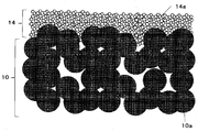
- FIG. 1 is a diagram schematically showing a semiconductor photoelectrode according to this embodiment in which a protective film is formed.
- FIG. 2 is a diagram schematically showing a conventional semiconductor photoelectrode in which no protective film is formed.
- FIG. 3 is a diagram schematically showing a dye-sensitized photoelectrochemical cell according to this embodiment.
- the semiconductor photoelectrode includes a current collector made of a porous metal sheet having pores communicating with the front and back surfaces, and a porous semiconductor layer adsorbed with a dye, which is laminated on the current collector.
- the current collector is covered with a protective film at least in part other than the portion in contact with the porous semiconductor layer.
- the porous metal sheet is a porous self-supporting metal substrate.
- a porous self-supporting metal substrate is a substrate made of a metal having sufficient strength and rigidity that can withstand the manufacturing process of forming a porous semiconductor thin film on the substrate as a substrate.
- the substrate has an appropriate thickness according to the species.
- the porous free-standing metal substrate is easy to handle as a current collector material. If the porous metal sheet is extremely porous, that is, extremely porous, the strength and rigidity may be impaired. On the other hand, if the porous metal sheet has an extremely low porosity, the liquid permeability of the electrolytic solution may be impaired.
- the porosity of the porous metal sheet is preferably in the range of 10 to 90%, more preferably in the range of 20 to 80%. Yes.
- the porous metal sheet has a thickness of preferably 5 ⁇ m or more, more preferably 25 ⁇ m, and even more preferably 100 ⁇ m or more. However, if the thickness is too thick, the cost is increased and cracks are liable to occur. Therefore, the thickness is preferably 10 mm or less.
- the porous metal sheet has an average pore diameter of preferably 5 ⁇ m to 25 ⁇ m, more preferably 5 ⁇ m to 15 ⁇ m.
- the average pore diameter of the porous metal sheet is significantly less than 5 ⁇ m, when used in a dye-sensitized photoelectrochemical cell, the flow resistance of the electrolyte inside the porous metal sheet increases, The flowability and diffusibility of the electrolyte inside or between both surfaces are deteriorated, which may impair the uniform penetration of the electrolyte into the porous metal sheet.
- the average pore diameter of the porous metal sheet greatly exceeds 25 ⁇ m, the strength may be impaired.
- the average pore diameter is excessively large, the area of the non-voided portion is also increased, so that the uniform distribution of the electrolyte inside the porous metal sheet and the opening of the porous metal sheet to the porous semiconductor layer Uniform diffusion may be hindered.
- the average pore diameter is a value when measured by a mercury intrusion method.
- Mercury intrusion type pore distribution measuring device (Pascal I 140 and Pascal by CARLOERBA INSTRUMENTS) 440, measurable range: specific surface area 0.1 m 2 / g or more, pore distribution 0.0034 to 400 ⁇ m), pressure range 0.3 to 400 kPa, and 0.1 to 400 MPa
- the cylindrical pore model it is calculated as a side area, integrated and measured.
- the porosity is calculated from the thickness of the porous metal sheet, the volume (A) calculated from the area, the mass (W), and the true density ( ⁇ ) by the following equation.
- the porous metal sheet is not particularly limited as long as the metal species has conductivity, but pure metals such as titanium, tantalum, niobium, zirconium and the like, which are metal species having higher conductivity, and those It is preferable to select and use an alloy containing at least one of them, or a material coated with these metals. Of these, titanium and titanium alloys are more preferred because of their high corrosion resistance, acid resistance, and oxidation resistance.
- the porous metal sheet a non-porous metal sheet subjected to mechanical or chemical hole machining or a wire mesh can be used.
- a metal sintered body obtained by sintering particulate metal or wire-like metal so-called sponge metal or anodized metal, and among these, it is more preferable to use a particulate metal sintered body.
- the metal sintered body can easily obtain an appropriate porosity, and can be made thin, and fine pores are uniformly distributed over the entire surface of the sheet.
- the electrolyte solution has more uniform and good liquid permeability when used in a dye-sensitized photoelectrochemical cell. It can be suitably obtained.
- the metal sintered body has a larger surface roughness than that of a metal mesh or the like, the adhesion strength between the porous metal sheet (metal sintered body) and the protective film is high.
- the porosity and surface roughness of a metal sintered compact can be adjusted, for example by pressurization or extending
- the porous semiconductor layer as a material, but can be used for ZnO or SnO 2 or the like as appropriate, TiO 2 is preferred.
- the shape and particle size of fine particles of TiO 2 and the like are not particularly limited, but are preferably about 1 nm to 100 nm.
- a dye is adsorbed on the surface of the fine particles constituting the porous semiconductor layer.
- the dye has absorption in at least a part of a wavelength region of 400 nm to 1000 nm, and examples thereof include metal complexes such as ruthenium dye and phthalocyanine dye, and organic dyes such as cyanine dye.
- the protective film is a film that can suppress a leakage current from the current collector.
- an insulator a semiconductor having a conduction band negatively larger than that of the metal oxide of the porous metal sheet, metal fine particles that can be in a surface plasmon excited state, and the like can be used.
- a semiconductor having a negative conduction band larger than that of the metal oxide of the porous metal sheet is used.
- the latter semiconductor is formed by forming a film having a higher energy level than the oxide film formed on the surface of the porous metal sheet, thereby making it more difficult for electrons to move between the porous metal sheet and the electrolyte. Leakage current from the electric body can be suppressed.
- the insulator examples include ceramics such as silicon oxide and aluminum oxide silica alumina, and polymers such as polyethylene and polypropylene.
- the metal species of the porous metal sheet is titanium, tantalum oxide, niobium oxide, and oxide having a larger conduction band than titanium oxide are used as the semiconductor having a larger conduction band than the metal oxide of the porous metal sheet. Zirconium etc. are mentioned. Further, the present invention is not limited to this, and composite compounds and non-oxides can be used.
- the protective film may be a combination of an insulator and a semiconductor. For example, tantalum oxide and polyethylene can be used in combination.
- the protective film is preferably an oxide containing at least one selected from silicon, aluminum, tantalum, niobium and zirconium.
- the thickness of the protective film is preferably 1 nm to 5000 nm, more preferably 10 nm to 2000 nm. If the thickness of the protective film is less than 1 nm, the effect of the protective film may be impaired. On the other hand, even if the thickness exceeds 5000 nm, it is not necessarily expected that the effect of the protective film is further increased.
- the protective film covers all portions other than the portion in contact with the porous semiconductor layer of the current collector. That is, not only the surface of the current collector on the side opposite to the side in contact with the porous semiconductor layer, but also the wall of the pores inside the current collector, in other words, for example, in the case of a sintered body, the entire particle surface
- a protective film it is desirable that all parts in contact with the electrolytic solution when used in a dye-sensitized photoelectrochemical cell are covered with a protective film.
- a coating may be cumbersome, and the entire surface coating may not dramatically improve the leakage current suppression effect. It is sufficient to cover a part of the area.
- the current collector coverage of the protective film is suitably 80% or more, for example.
- a photoelectrode (semiconductor photoelectrode) according to the present embodiment in which a protective film is formed is schematically shown in FIG. 1, and together with this, a conventional photoelectrode without a protective film is schematically shown in FIG.
- reference numeral 10 denotes a current collector made of a particle sintered body
- reference numeral 10a denotes a particle constituting the current collector
- reference numeral 12 denotes a protective film covering the particles constituting the current collector.
- Reference numeral 14 represents a porous semiconductor layer
- reference numeral 14a represents a semiconductor particle constituting the porous semiconductor layer.
- the pores that are the gaps between the particles 10a constituting the current collector surface and the current collector inside the current collector are in contact with the electrolytic solution.
- the protective film 12 separates the surface of the current collector 10 and the particles 10a constituting the current collector inside the current collector from the electrolytic solution.
- the semiconductor photoelectrode for dye-sensitized photoelectrochemical cell according to the present embodiment described above has sufficient electrical connection with the porous semiconductor layer when used in a dye-sensitized photoelectrochemical cell. In addition, the generation of leakage current from the current collector to the electrolyte can be efficiently suppressed.
- the semiconductor photoelectrode for dye-sensitized photoelectrochemical cell according to the present embodiment when the current collector is provided on the porous support layer made of a ceramic plate or the like as described in Patent Document 4, It is not sufficient in that the wall portion of the pores inside the current collector is not protected and the liquid permeability of the electrolyte is impaired due to the liquid flow resistance of the porous support layer.
- the semiconductor photoelectrode for dye-sensitized photoelectrochemical cell according to this embodiment which can suitably obtain the semiconductor photoelectrode for dye-sensitized photoelectrochemical cell according to this embodiment.
- a manufacturing method will be described.
- the method for producing a semiconductor photoelectrode for a dye-sensitized photoelectrochemical cell masks one side of a porous metal sheet, which is a current collector material, having pores communicating with the front and back, A first step of forming a protective film on the porous metal sheet; a second step of removing the mask; and a third step of forming a porous semiconductor layer having a dye adsorbed on one side from which the mask has been removed. Including.
- porous metal sheet used in the first step is the same as that described for the semiconductor photoelectrode for dye-sensitized photoelectrochemical cell according to the present embodiment, a redundant description is omitted.
- the mask is preferably a resin film that can be easily removed mechanically or chemically, but is not limited to this, and a liquid mask such as a resin varnish or resin ink can be used.
- a thermoplastic resin such as a polyimide resin and its precursor, a polyvinyl resin, a polyester resin, a polyether resin, a polyamide resin, a fluorine resin, an ionomer resin, a solder resist film, or the like is used.
- the resin ink it is possible to use a varnish obtained by dissolving the thermosetting resin or a precursor thereof in an organic solvent, a solder resist ink, or the like.
- a resin film that decomposes during heat treatment when forming the protective film because the manufacturing process can be shortened.
- a resin paste may be applied to the current collector by screen printing or the like.
- the method for forming the protective film on the porous metal sheet is not particularly limited, but it is preferable to use a method in which the porous metal sheet is impregnated with the protective film raw material liquid. It is also preferable to use an atomic layer deposition method, a CVD method, a PVD method, or the like as a method or a plating method or a dry method.
- the protective film raw material liquid impregnated with the porous metal sheet is a metal salt of the protective film material described for the semiconductor photoelectrode for dye-sensitized photoelectrochemical cell according to the present embodiment, for example, alcohol or the like Those dissolved in the above solvent can be used.
- the porous metal sheet impregnated with the protective film raw material liquid is dried, for example, at a temperature of about 150 ° C. for about one hour in a high temperature drying chamber, thereby volatilizing the solvent component of the protective film raw material liquid.
- heat treatment is performed at a temperature of about 500 ° C. for about 1 hour, thereby forming an oxide film of a protective film material metal.
- post-coating post-treatment similar to the above is also performed in wet methods other than the impregnation method. On the other hand, in the case of the dry method, such post-treatment is not necessary.
- the drying of the porous metal sheet in the second step is performed, for example, at a temperature of about 150 ° C. for about 1 hour in a high-temperature drying chamber, thereby volatilizing the solvent component of the protective film raw material liquid.
- heat treatment is performed at a temperature of about 500 ° C. for about 1 hour, thereby forming an oxide film of a protective film material metal.
- Removal of the mask may be performed after the precursor of the protective film is applied and before the precursor is heated, or may be performed after the precursor is heated.
- a chemical removal method a dissolution peeling method using a chemical such as an acid, an alkali, or an organic solvent can be used.
- the porous metal sheet and the porous semiconductor layer are reliably brought into contact with each other. Therefore, instead of forming a protective film on a desired portion of the porous metal sheet by the above-described methods, a protective film is formed on the entire surface of the porous metal sheet, and then a part of the protective film is scraped off to form a metal.
- a method of exposing the surface can also be used. Examples of the scraping method include mechanical polishing such as a grindstone, sand blasting, and laser scribing.
- porous semiconductor layer used in the third step is the same as that described for the semiconductor photoelectrode for dye-sensitized photoelectrochemical cell according to the present embodiment, a redundant description is omitted.
- a porous semiconductor layer is obtained by firing at a temperature of 300 to 550 ° C., for example.
- the method of adsorption onto the porous semiconductor layer is not particularly limited.
- a so-called dye solution is impregnated with a porous metal sheet in which the porous semiconductor layer 1 is formed, and the dye is chemically adsorbed on the surface of semiconductor fine particles such as TiO 2.
- An impregnation method can be used.
- the semiconductor photoelectrode for dye-sensitized photoelectrochemical cell according to this embodiment is suitably obtained by the method for manufacturing a semiconductor photoelectrode for dye-sensitized photoelectrochemical cell according to this embodiment described above. be able to.
- a dye-sensitized photoelectrochemical cell 16 according to the present embodiment schematically shown in FIG. 3 includes a transparent substrate 18, a conductive substrate (counter electrode) 20 serving as a cathode electrode, a transparent substrate 18, and a conductive substrate. 20, the porous semiconductor layer 22 laminated on the current collector 24 is disposed in the vicinity of or in contact with the transparent substrate 18, and serves as an anode electrode.
- the semiconductor photoelectrode 26 for chemical cells is provided.
- reference numeral 28 denotes a spacer
- reference numeral 30 denotes an electrolytic solution to be sealed
- reference numeral 32 denotes a conductive wire that is connected to the current collector 24 and serves as a lead electrode.
- the spacer 28 also functions as a strength auxiliary substrate for the semiconductor photoelectrode 26 for dye-sensitized photoelectrochemical cell.
- dye which provided the transparent conductive film in the transparent substrate 18 for the semiconductor photoelectrode for dye-sensitized photoelectrochemical cells which concerns on this Embodiment. Needless to say, application to a sensitized photoelectrochemical cell is not excluded.
- the transparent substrate 18 may be, for example, a glass plate or a plastic plate.
- a plastic plate When a plastic plate is used, flexibility can be imparted to the dye-sensitized solar cell, which is preferable.
- a plastic plate for example, PET, PEN, polyimide, a cured acrylic resin, a cured epoxy resin, a cured silicone resin, various engineering plastics, a cyclic polymer obtained by metathesis polymerization, and the like can be given.
- the transparent substrate 18 constitutes a part of a light-transmitting resin film that covers the entire cell.
- ITO indium oxide film doped with tin
- FTO fluorine doped, etc.
- flop tin oxide film), SnO 2 film, Ti, W, Mo may be used as the laminated Rh, Pt, a conductive film of a metal film of Ta or the like.
- the conductive substrate 20 is the same substrate as the transparent substrate 12, and is formed on, for example, an ITO, FTO, SnO 2 film, Ti, W, Mo, Rh, A conductive film such as a metal film such as Pt or Ta is laminated, and a catalyst film such as a platinum film is provided on the conductive film. Further, the transparent substrate may be omitted, and a catalyst film such as a platinum film may be provided on the metal foil.
- the metal foil is preferably Ti.
- the electrolytic solution 30 is not particularly limited, and includes, for example, iodine, lithium ions, ionic liquid, t-butylpyridine, and the like.
- iodine an oxidation-reduction body composed of a combination of iodide ions and iodine is used. be able to.
- a metal complex such as cobalt may be used as the redox pair.
- it contains a solvent capable of dissolving this redox substance, and examples thereof include acetonitrile, ⁇ -butyrolactone, propionitrile, ethylene carbonate, and ionic liquid.
- Maximum particle size, average particle size measurement method For maximum particle size and average particle size (50% particle size in the volume cumulative particle size distribution), use a laser diffraction particle size distribution analyzer (LA-300 manufactured by Beckman Coulter, Inc.) and put the measurement sample into the flow cell. And measured. (Thickness measurement method) The thickness of the obtained porous titanium thin film (rectangular shape) was measured at three places at equal intervals in three directions, for a total of nine places, and the average value was obtained. The three directions are the central portion, the upper side portion, and the lower side portion of the porous titanium thin film.
- a porous titanium metal plate having a planar size of 5 ⁇ 20 mm and a thickness of 200 ⁇ m (Typorus 45 manufactured by Osaka Titanium Co., Ltd., an average particle size of 25 ⁇ m, an average pore size of about 10 ⁇ m) is used as a current collector.
- Infiltrate the coating solution (Symmetrics, MOD coating solution, diluted to 0.1M), and dry at 150 ° C. for 1 hour, and then heat-treat in air at 500 ° C. for 1 hour.
- a protective film made of a metal oxide was formed on the surface of the porous titanium metal substrate.
- heat treatment was performed at 500 ° C. for 1 hour without using a coating solution.
- the purity of the protective film material metal (main component) shown in Table 1 is about 90% by mass or more.
- electrochemical measurement was performed by the following method.
- a 3 mm edge on the surface of the porous titanium metal substrate on which the protective film was formed was polished with a file to remove the protective film, and stopped with a hook clip to obtain a working electrode.
- the counter electrode was a Pt wire.
- An electrolyte solution was prepared by dissolving 0.1M lithium iodide, 0.05M iodine, and 0.62M dimethylpropylimidazolium iodide in a solvent of acetonitrile.
- the measurement was performed with a potentiostat bipolar.
- the tip 1 cm 2 of the working electrode was brought into contact with the electrolyte solution.
- the potential was swept between 0V and -0.8V, and the leakage current and the ability to suppress the current leakage were examined by measuring the cathode current in which electrons flow from the porous titanium metal substrate to iodine in the electrolyte. The results are shown in Table 1.
- the aluminum oxide and silicon oxide of Examples 1 and 2 are insulators.
- Niobium oxide, tantalum oxide and zirconium oxide of Example 3-5 are semiconductors having a negative conduction band larger than that of titanium oxide.
- the conduction band of bismuth oxide of Comparative Example 2 is more positive than the conduction band of titanium oxide. It can be seen that any of Examples 1 to 5 has a smaller cathode current than Comparative Example 1 without a protective film, and has an effect of preventing leakage current from the current collector. Further, it can be seen that Comparative Example 2 has a larger cathode current than Examples 1-5 and Comparative Example 1, and has no effect of preventing leakage current from the substrate.
- thermoplastic resin film After pasting a thermoplastic resin film on one side of a porous titanium metal plate having a planar size of 20 ⁇ 30 mm and a thickness of 100 ⁇ m (Typorus 45 manufactured by Osaka Titanium Co., Ltd., average particle diameter of 25 ⁇ m, average pore diameter of about 10 ⁇ m), A coating solution (manufactured by Symmetrics, MOD coating solution, diluted to 0.1 M) in which the protective film material metal shown was soaked and dried at 150 ° C. for 1 hour, and then the thermoplastic resin film was peeled off. Then, a metal oxide protective film was formed on the surface of the porous titanium metal substrate by heat treatment in air at 500 ° C. for 1 hour.
- a Ti-Nanoxide-D paste was applied in a range of 5 mm ⁇ 20 mm on the surface of the porous titanium metal substrate on which the thermoplastic film was peeled off, and baked in air at 400 ° C. for 30 minutes. This was repeated 3 to 4 times to form a TiO 2 layer (porous semiconductor layer).
- the N719 dye was adsorbed on the TiO 2 layer by a so-called impregnation method in which the N719 dye was immersed in a solvent in which the N719 dye was dissolved.
- a PET substrate, an adhesive sheet composed of an ionomer resin, an insulating layer, and a Pt / ITO / PET counter electrode are laminated.
- the solvent is acetonitrile and lithium iodide 0.1M, iodine 0.05M, dimethylpropyl iodide
- a dye-sensitized photoelectrochemical cell was prepared by injecting imidazolium 0.62M and t-butylpyridine to a concentration of 0.5M and dissolving the electrolyte.
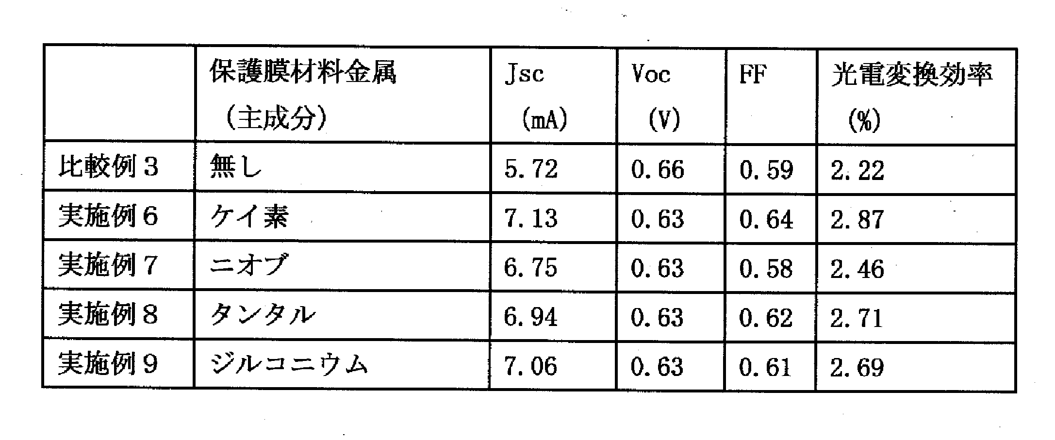
- Table 2 shows the results of photoelectric conversion efficiency and the like of the dye-sensitized photoelectrochemical cell obtained by irradiating simulated solar light of AM1.5, 1SUN (100 mW / cm 2 ) using a solar simulator. Show.
Landscapes
- Engineering & Computer Science (AREA)
- Power Engineering (AREA)
- Microelectronics & Electronic Packaging (AREA)
- Chemical & Material Sciences (AREA)
- Chemical Kinetics & Catalysis (AREA)
- Electrochemistry (AREA)
- Hybrid Cells (AREA)
- Photovoltaic Devices (AREA)
Abstract
集電電極からの漏れ電流を十分に抑制できる、色素増感型光電気化学セル用半導体光電極およびこれを用いた、透明導電膜を省略した色素増感型光電気化学セルを提供する。 色素増感型光電気化学セルに用いる半導体光電極は、表裏に連通する細孔を持つ多孔質金属シートからなる集電体10と、集電体10に積層される、色素を吸着した多孔質半導体層14を含み、集電体10の多孔質半導体層14と接する部分を除く他の部分の少なくとも一部が保護膜12で被覆される。色素増感型光電気化学セルは、透明基板と、カソード極となる導電性基板の間に、多孔質半導体層14を透明基板に近接してまたは接触して配置され、アノード極となる半導体光電極を備える。
Description
本発明は、色素増感型光電気化学セル用半導体光電極およびその製造方法ならびに色素増感型光電気化学セルに関する。
一般的な色素色素増感太陽電池(色素増感型光電気化学セル)の発電メカニズムは、以下のとおりである。
入射した光を、多孔質半導体層に吸着された色素が吸収し、電子励起を引き起こし、その励起した電子が半導体(多孔質半導体層)へと移動し、集電電極(集電体)へと導かれる。ついで、集電電極に接続される外部回路を介して対極に戻った電子は電解液を介して電子を失った色素へと導かれ、色素が再生される。
しかし、このとき、集電電極へ導かれた電子が、外部回路に移動せず、電解液中に漏れてしまう、いわゆる漏れ電流を発生する問題があった。
入射した光を、多孔質半導体層に吸着された色素が吸収し、電子励起を引き起こし、その励起した電子が半導体(多孔質半導体層)へと移動し、集電電極(集電体)へと導かれる。ついで、集電電極に接続される外部回路を介して対極に戻った電子は電解液を介して電子を失った色素へと導かれ、色素が再生される。
しかし、このとき、集電電極へ導かれた電子が、外部回路に移動せず、電解液中に漏れてしまう、いわゆる漏れ電流を発生する問題があった。
一般に、半導体材料を加熱して多孔質半導体層を形成する際に、多孔質半導体層が積層される集電電極表面には酸化膜ができるために、漏れ電流はある程度は抑制される。しかし、酸化膜の微小な欠陥等に起因する小さな漏れ電流でも、電圧やフィルファクターおよび効率の低化を招く。特に、集電電極が大型化または大表面積化した場合には、効率の低下は顕著になると考えられる。
この漏れ電流を抑制する方法として、透明導電膜に電気的に接続された金属配線層(集電体)の表面をガラスや耐熱セラミックを主成分とする絶縁層で被覆する技術が開示されている(特許文献1、2)。また、透明導電層に積層した金属配線層を内層と外層の2層で構成し、外層を内層との結合部位をなす末端の官能基に硫黄元素を含む自己組織化膜等とする技術が開示されている(特許文献3)。
これに対して、光透過を高めるために、透明導電膜を省略した色素増感太陽電池、すなわち、光照射側となる透明導電膜を持たない透明基板に多孔質半導体層を形成し、多孔質半導体層の上に有孔集電電極を配置した色素増感太陽電池が広く検討されている。この透明導電膜を持たない色素増感太陽電池では、有孔集電電極が、上記透明導電層の代わりとして多孔質半導体層との十分な電気的接続を図ることが求められる。このため、上記のような漏れ電流を抑制する技術は適用が困難であった。
ところで、本出願人らは、多孔質半導体層が積層される多孔質導電性金属層(集電体)として、薄膜形成法による薄膜をセラミック板等からなる多孔質支持層上に設ける技術を開示している(特許文献4)。ここで用いる多孔質支持層は薄膜を形成する際の基材の役割を果たすとともに、薄膜を支持して強度を補強する役割を果たすものである。しかし、この多孔質支持層は、結果的に、漏れ電流を抑制する保護膜としても機能しているといえる。
解決しようとする問題点は、従来の透明導電膜を省略した色素増感太陽電池では、集電電極からの漏れ電流を十分に抑制できない点である。
本発明者らは、上記課題を解決するために鋭意検討した結果、裏表につながる細孔を持つ多孔質金属シートからなる集電体を用い、その集電体の少なくとも一部に保護膜を付けると、集電体から電解質への漏れ電流を効率良く防止されることを見出し、本発明を完成するに至った。
本発明に係る色素増感型光電気化学セル用半導体光電極は、表裏に連通する細孔を持つ多孔質金属シートからなる集電体と、該集電体に積層される、色素を吸着した多孔質半導体層を含み、
該集電体の該多孔質半導体層と接する部分を除く他の部分の少なくとも一部が保護膜で被覆されてなることを特徴とする。
該集電体の該多孔質半導体層と接する部分を除く他の部分の少なくとも一部が保護膜で被覆されてなることを特徴とする。
また、本発明に係る色素増感型光電気化学セル用半導体光電極は、好ましくは、前記集電体がチタンまたはチタン合金で形成されてなることを特徴とする。
また、本発明に係る色素増感型光電気化学セル用半導体光電極は、好ましくは、前記集電体が粒子状の金属を焼結させた金属焼結体であることを特徴とする。
また、本発明に係る色素増感型光電気化学セル用半導体光電極は、好ましくは、前記保護膜が絶縁体または前記多孔質金属シートの金属の酸化物よりも伝導帯が負に大きい半導体であることを特徴とする。
また、本発明に係る色素増感型光電気化学セル用半導体光電極は、好ましくは、前記保護膜がケイ素、アルミニウム、タンタル、ニオブおよびジルコニウムから選ばれる少なくとも一種を含む金属の酸化物で形成されてなることを特徴とする。
また、本発明に係る色素増感型光電気化学セル用半導体光電極の製造方法は、表裏に連通する細孔を持つ、集電体材料である多孔質金属シートの片面をマスクした後、該多孔質金属シートに保護膜を形成する第一の工程と、
該マスクを除去する第二の工程と、
マスクを除去した該片面に色素を吸着した多孔質半導体層を形成する第三の工程と、
を含むことを特徴とする。
該マスクを除去する第二の工程と、
マスクを除去した該片面に色素を吸着した多孔質半導体層を形成する第三の工程と、
を含むことを特徴とする。
また、本発明に係る色素増感型光電気化学セルは、透明基板と、カソード極となる導電性基板と、該透明基板と該導電性基板の間に、集電体に積層される多孔質半導体層を該透明基板に近接してまたは接触して配置され、アノード極となる上記の色素増感型光電気化学セル用半導体光電極を備え、電解質が封止されてなることを特徴とする。
本発明に係る色素増感型光電気化学セル用半導体光電極は、集電体の多孔質半導体層と接する部分を除く他の部分の少なくとも一部が保護膜で被覆されるため、色素増感型光電気化学セルに用いたときに、集電体から電解質への漏れ電流を効率良く防止することができる。
また、本発明に係る色素増感型光電気化学セル用半導体光電極の製造方法は、表裏に連通する細孔を持つ、集電体材料である多孔質金属シートの片面をマスクした後、多孔質金属シートに保護膜を形成する第一の工程と、マスクを除去する第二の工程と、マスクを除去した片面に色素を吸着した多孔質半導体層を形成する第三の工程と、を含むため、本発明に係る色素増感型光電気化学セル用半導体光電極を好適に得ることができる。
また、本発明に係る色素増感型光電気化学セルは、本発明に係る色素増感型光電気化学セル用半導体光電極を備えるため、本発明に係る色素増感型光電気化学セル用半導体光電極の効果を好適に得ることができる。
また、本発明に係る色素増感型光電気化学セル用半導体光電極の製造方法は、表裏に連通する細孔を持つ、集電体材料である多孔質金属シートの片面をマスクした後、多孔質金属シートに保護膜を形成する第一の工程と、マスクを除去する第二の工程と、マスクを除去した片面に色素を吸着した多孔質半導体層を形成する第三の工程と、を含むため、本発明に係る色素増感型光電気化学セル用半導体光電極を好適に得ることができる。
また、本発明に係る色素増感型光電気化学セルは、本発明に係る色素増感型光電気化学セル用半導体光電極を備えるため、本発明に係る色素増感型光電気化学セル用半導体光電極の効果を好適に得ることができる。
本発明の実施の形態(以下、本実施の形態例という。)について、以下に説明する。
まず、本実施の形態例に係る色素増感型光電気化学セル用半導体光電極(以下、これを単に半導体光電極ということがある。)について説明する。
半導体光電極は、表裏に連通する細孔を持つ多孔質金属シートからなる集電体と、集電体に積層される、色素を吸着した多孔質半導体層を含む。集電体は多孔質半導体層と接する部分を除く他の部分の少なくとも一部が保護膜で被覆される。
多孔質金属シートは、言い換えれば、多孔性自立金属基板である。多孔性自立金属基板は、基板としてその上に多孔質半導体薄膜を形成する製造プロセスに耐えうる充分な強度や剛性を持つ金属でできた基板をいい、この特性を発現するのに必要な、金属種に応じた適宜の厚みを持つ基板である。多孔性自立金属基板は、集電体の材料としてのハンドリングも容易である。
多孔質金属シートは、極端に多孔質、すなわち極端に空隙率の高いものであると、強度や剛性が損なわれるおそれがある。一方、多孔質金属シートは、極端に空隙率の低いものであると、電解液の通液性が損なわれるおそれがある。このため、多孔質金属シートは、空隙率を10~90%の範囲とすることが好ましく、20~80%の範囲がより好ましい。い。また、多孔質金属シートは、厚みを、好ましくは5μm以上、より好ましくは25μm、さらに好ましくは100μm以上とする。ただし、厚みが極端に厚すぎるとコストが高くなり、またクラックを生じやすくなるので、10mm以下の厚さとすることが好ましい。
多孔質金属シートは、極端に多孔質、すなわち極端に空隙率の高いものであると、強度や剛性が損なわれるおそれがある。一方、多孔質金属シートは、極端に空隙率の低いものであると、電解液の通液性が損なわれるおそれがある。このため、多孔質金属シートは、空隙率を10~90%の範囲とすることが好ましく、20~80%の範囲がより好ましい。い。また、多孔質金属シートは、厚みを、好ましくは5μm以上、より好ましくは25μm、さらに好ましくは100μm以上とする。ただし、厚みが極端に厚すぎるとコストが高くなり、またクラックを生じやすくなるので、10mm以下の厚さとすることが好ましい。
また、多孔質金属シートは、平均細孔径が、好ましくは5μm~25μmであり、さらに好ましくは5μm~15μmである。多孔質金属シートの平均細孔径が5μmを大きく下回ると、色素増感型光電気化学セルに用いたときに、多孔質金属シート内部での電解液の流動抵抗が大きくなって多孔質金属シートの内部あるいは両面間での電解質の流通性や拡散性が悪くなり、これにより、多孔質金属シートへの電解質の均一な浸透が損なわれるおそれがある。一方、多孔質金属シートの平均空孔直径が25μmを大きく上回ると、強度が損なわれおそれがある。また、平均空孔直径が過度に大きくなると、非空孔部の面積も大きくなるので、多孔質金属シート内部の電解質の均一な流通および多孔質金属シートの開口から多孔質半導体層への電解質の均一な拡散が阻害されるおそれがある。
なお、平均空孔直径は、水銀圧入法により測定するときの値である。水銀圧入式細孔分布測定装置(CARLOERBA INSTRUMENTS社製PascaI 140およびPascal
440、測定可能範囲:比表面積0.1m2/g以上、細孔分布0.0034~400μm)を用いて、圧力範囲0.3~400kPa、および0.1~400MPaの範囲で、圧入体積を円筒細孔モデルに従って、側面積として計算し積算して測定する。
また、空隙率は、多孔質金属シートの厚さと、面積から計算した体積(A)と、質量(W)と、真密度(ρ)より下式により算出する。
空隙率(%)=(1-W/Aρ)×100=(A-W/ρ)/A×100
440、測定可能範囲:比表面積0.1m2/g以上、細孔分布0.0034~400μm)を用いて、圧力範囲0.3~400kPa、および0.1~400MPaの範囲で、圧入体積を円筒細孔モデルに従って、側面積として計算し積算して測定する。
また、空隙率は、多孔質金属シートの厚さと、面積から計算した体積(A)と、質量(W)と、真密度(ρ)より下式により算出する。
空隙率(%)=(1-W/Aρ)×100=(A-W/ρ)/A×100
多孔質金属シートは、金属種としては、導電性を有するものであれば特に限定するものではないが、より高い導電性を有する金属種であるチタン、タンタル、ニオブ、ジルコニウムなどの純金属およびそれらのうちの少なくとも一つを含む合金、さらにはこれらの金属を被覆した材料の中から適宜選択して用いることが好ましい。中でもチタンおよびチタン合金は耐腐食性や耐酸性、耐酸化性が高いので、より好ましい。
多孔質金属シートは、非孔質金属シートに機械的あるいは化学的な孔加工を施したものや金網を用いることができる。ただし、粒子状の金属やワイヤ状の金属を焼結させた金属焼結体、いわゆるスポンジ金属あるいは陽極酸化金属を用いることが好ましく、このうち粒子状の金属の焼結体を用いることがより好ましい。金属焼結体は、金網等に比べて、適度の空隙率を容易に得ることができ、また、厚みを薄くすることができるとともに、微細な細孔がシート全面に均一に分布し、かつ細孔が表裏に連通するだけでなく面方向にも連通する三次元網目構造状であるため、色素増感型光電気化学セルに用いたときに電解液の均一でかつ良好な通液性をより好適に得ることができる。また、金属焼結体は、金網等に比べて表面粗度が大きいため、多孔質金属シート(金属焼結体)と保護膜との密着強度が高い。なお、金属焼結体の空隙率や表面粗度は、例えば加圧や、延伸することで調整できる。
多孔質半導体層は、材料として、ZnOやSnO2等適宜のものを用いることができるが、TiO2が好ましい。TiO2等の微粒子形状や粒径は特に限定するものではないが、1nm~100nm程度が好ましい。
多孔質半導体層を構成する微粒子の表面に、色素を吸着する。色素は、400nm~1000nmの波長領域の少なくとも一部に吸収を持つものであり、例えば、ルテニウム色素、フタロシアニン色素などの金属錯体、シアニン色素などの有機色素を挙げることができる。
多孔質半導体層を構成する微粒子の表面に、色素を吸着する。色素は、400nm~1000nmの波長領域の少なくとも一部に吸収を持つものであり、例えば、ルテニウム色素、フタロシアニン色素などの金属錯体、シアニン色素などの有機色素を挙げることができる。
保護膜は、集電体からの漏れ電流を抑制することができる膜である。保護膜は、絶縁体、多孔質金属シートの金属の酸化物よりも伝導帯が負に大きい半導体、表面プラズモン励起状態になり得る金属微粒子等を用いることができるが、好ましくは、絶縁体または多孔質金属シートの金属の酸化物よりも伝導帯が負に大きい半導体を用いる。後者の半導体は、多孔質金属シート表面に形成される酸化膜よりもエネルギー準位の高い膜を形成することで、多孔質金属シートと電解液間の電子の移動を一層困難とすることにより集電体からの漏れ電流を抑制することができる。
絶縁体としては酸化ケイ素や酸化アルミニウムシリカアルミナなどのセラミックやポリエチレンやポリプロピレンなどのポリマー等が挙げられる。
多孔質金属シートの金属の酸化物よりも伝導帯が負に大きい半導体としては、例えば多孔質金属シートの金属種がチタンの場合、酸化チタンより伝導帯が負に大きい酸化タンタル、酸化ニオブおよび酸化ジルコニウムなどが挙げられる。また、これに限らず、複合化合物や非酸化物を用いることができる。
保護膜は、絶縁体と半導体の組み合わせであってもよく、例えば、酸化タンタルとポリエチレンを組み合わせて用いることができる。また、熱安定性や耐薬品性を考慮すると、保護膜は、ケイ素、アルミニウム、タンタル、ニオブおよびジルコニウムから選ばれる少なくとも一種を含む酸化物が望ましい。
保護膜の厚みは、1nm~5000nmが好ましく、10nm~2000nmがさらに好ましい。保護膜の厚みが1nmを下回ると保護膜の効果が損なわれるおそれがあり、一方、5000nmを上回っても保護膜の効果がさらに増すことは必ずしも期待できない。
絶縁体としては酸化ケイ素や酸化アルミニウムシリカアルミナなどのセラミックやポリエチレンやポリプロピレンなどのポリマー等が挙げられる。
多孔質金属シートの金属の酸化物よりも伝導帯が負に大きい半導体としては、例えば多孔質金属シートの金属種がチタンの場合、酸化チタンより伝導帯が負に大きい酸化タンタル、酸化ニオブおよび酸化ジルコニウムなどが挙げられる。また、これに限らず、複合化合物や非酸化物を用いることができる。
保護膜は、絶縁体と半導体の組み合わせであってもよく、例えば、酸化タンタルとポリエチレンを組み合わせて用いることができる。また、熱安定性や耐薬品性を考慮すると、保護膜は、ケイ素、アルミニウム、タンタル、ニオブおよびジルコニウムから選ばれる少なくとも一種を含む酸化物が望ましい。
保護膜の厚みは、1nm~5000nmが好ましく、10nm~2000nmがさらに好ましい。保護膜の厚みが1nmを下回ると保護膜の効果が損なわれるおそれがあり、一方、5000nmを上回っても保護膜の効果がさらに増すことは必ずしも期待できない。
保護膜は、集電体の多孔質半導体層と接する部分以外の部分を全て被覆するものであることが望ましい。すなわち、集電体の多孔質半導体層と接する側と反対側の表面のみでなく、集電体の内部の細孔の壁部言い換えれば例えば焼結体の場合であれば粒子表面の全てが、すなわち、色素増感型光電気化学セルに用いたときに電解液に接する全ての部分が保護膜で被覆されることが望ましい。ただし、このような被覆を行うことは処理が煩雑となる場合があり、また、全面被覆を行うことで漏れ電流の抑制効果が飛躍的に向上するとも限らないため、煩雑とならない処理法で可能な範囲で部分的に被覆すれば足りる。保護膜の集電体被覆率は、例えば、80%以上とすることが適当である。
保護膜を形成した本実施の形態例に係る光電極(半導体光電極)を模式的に図1に示し、これと合わせて、保護膜を形成していない従来の光電極を模式的に図2に示す。図1および図2中、参照符号10は粒子焼結体からなる集電体を、参照符号10aは集電体を構成する粒子を、参照符号12は集電体を構成する粒子を覆う保護膜を、参照符号14は多孔質半導体層を、参照符号14aは多孔質半導体層を構成する半導体粒子を、それぞれ示す。
光電極を色素増感型光電気化学セルに組み込んだ状態において、集電体10の表面および集電体内部の集電体を構成する粒子10a間の隙間である細孔は電解液に接するが、図1の光電極では保護膜12により集電体10の表面および集電体内部の集電体を構成する粒子10aは電解液と隔てられる。
保護膜を形成した本実施の形態例に係る光電極(半導体光電極)を模式的に図1に示し、これと合わせて、保護膜を形成していない従来の光電極を模式的に図2に示す。図1および図2中、参照符号10は粒子焼結体からなる集電体を、参照符号10aは集電体を構成する粒子を、参照符号12は集電体を構成する粒子を覆う保護膜を、参照符号14は多孔質半導体層を、参照符号14aは多孔質半導体層を構成する半導体粒子を、それぞれ示す。
光電極を色素増感型光電気化学セルに組み込んだ状態において、集電体10の表面および集電体内部の集電体を構成する粒子10a間の隙間である細孔は電解液に接するが、図1の光電極では保護膜12により集電体10の表面および集電体内部の集電体を構成する粒子10aは電解液と隔てられる。
以上説明した本実施の形態例に係る色素増感型光電気化学セル用半導体光電極は、色素増感型光電気化学セルに用いたときに、多孔質半導体層との電気的接続を十分に確保したうえで、集電体から電解質への漏れ電流の発生を効率良く抑制することができる。
なお、本実施の形態例に係る色素増感型光電気化学セル用半導体光電極において、前記した特許文献4のように集電体をセラミック板等からなる多孔質支持層上に設けた場合、集電体の内部の細孔の壁部が保護されず、また、多孔質支持層の通液抵抗により電解液の通液性が損なわれる点において十分ではない。
なお、本実施の形態例に係る色素増感型光電気化学セル用半導体光電極において、前記した特許文献4のように集電体をセラミック板等からなる多孔質支持層上に設けた場合、集電体の内部の細孔の壁部が保護されず、また、多孔質支持層の通液抵抗により電解液の通液性が損なわれる点において十分ではない。
つぎに、上記本実施の形態例に係る色素増感型光電気化学セル用半導体光電極を好適に得ることができる本実施の形態例に係る色素増感型光電気化学セル用半導体光電極の製造方法について説明する。
本実施の形態例に係る色素増感型光電気化学セル用半導体光電極の製造方法は、表裏に連通する細孔を持つ、集電体材料である多孔質金属シートの片面をマスクした後、多孔質金属シートに保護膜を形成する第一の工程と、マスクを除去する第二の工程と、マスクを除去した片面に色素を吸着した多孔質半導体層を形成する第三の工程と、を含む。
本実施の形態例に係る色素増感型光電気化学セル用半導体光電極の製造方法は、表裏に連通する細孔を持つ、集電体材料である多孔質金属シートの片面をマスクした後、多孔質金属シートに保護膜を形成する第一の工程と、マスクを除去する第二の工程と、マスクを除去した片面に色素を吸着した多孔質半導体層を形成する第三の工程と、を含む。
第一の工程で用いる多孔質金属シートは、本実施の形態例に係る色素増感型光電気化学セル用半導体光電極について説明したものと同様であるため、重複する説明を省く。
マスクは、機械的にあるいは化学的に容易に除去可能な樹脂フィルムを用いることが好ましいが、これに限らず、樹脂ワニス、樹脂インク等の液状マスク等を用いることができる。
樹脂フィルムの樹脂として、ポリイミド系樹脂およびその前駆体、ポリビニル系樹脂、ポリエステル系樹脂、ポリエーテル系樹脂、ポリアミド系樹脂、フッ素系樹脂等の熱可塑性樹脂やアイオノマー樹脂、ソルダーレジストフィルム等を用いることができる。また、樹脂インクとして、上記熱硬化性樹脂またはこれらの前駆体を有機溶剤に溶解させたワニス、ソルダーレジストインク等を用いることができる。なお、保護膜を形成する際の熱処理時に分解するような樹脂フィルムを用いると、製造工程を短縮することができるので好ましい。樹脂フィルムを集電体に貼付する代わりに、樹脂ペーストをスクリーン印刷などで集電体に塗布してもよい。
樹脂フィルムのフロー性により、あるいは液状マスクの浸透性を制御することにより、集電体の細孔の奥深くまでマスクできる。
樹脂フィルムの樹脂として、ポリイミド系樹脂およびその前駆体、ポリビニル系樹脂、ポリエステル系樹脂、ポリエーテル系樹脂、ポリアミド系樹脂、フッ素系樹脂等の熱可塑性樹脂やアイオノマー樹脂、ソルダーレジストフィルム等を用いることができる。また、樹脂インクとして、上記熱硬化性樹脂またはこれらの前駆体を有機溶剤に溶解させたワニス、ソルダーレジストインク等を用いることができる。なお、保護膜を形成する際の熱処理時に分解するような樹脂フィルムを用いると、製造工程を短縮することができるので好ましい。樹脂フィルムを集電体に貼付する代わりに、樹脂ペーストをスクリーン印刷などで集電体に塗布してもよい。
樹脂フィルムのフロー性により、あるいは液状マスクの浸透性を制御することにより、集電体の細孔の奥深くまでマスクできる。
多孔質金属シートに保護膜を形成する方法は、特に限定するものではないが、多孔質金属シートに保護膜原料液を含浸する方法を用いることが好ましく、また、湿式法として、スプレー法、塗布法あるいはメッキ法等や、さらに乾式法として、アトミックレーヤーデポジション法、CVD法、PVD法等を用いることも好ましい。
含浸法の場合、多孔質金属シートを含浸する保護膜原料液は、本実施の形態例に係る色素増感型光電気化学セル用半導体光電極について説明した保護膜材料の金属塩を例えばアルコール等の溶媒に溶解したものを用いることができる。多孔質金属シートを例えば室温℃程度の温度の保護膜原料液に例えば0.1時間程度含浸することで、集電体の細孔の奥深くまで保護膜原料液を浸透させることができる。
この場合、保護膜原料液を含浸した多孔質金属シートを、例えば、高温乾燥室内で150℃程度の温度で1時間程度乾燥して、これにより保護膜原料液の溶媒成分を揮発する。ついで、500℃程度の温度で1時間程度熱処理して、これにより保護膜材料金属の酸化膜を形成する。
なお、含浸法以外の湿式法においても上記に準じた塗布後の後処理を行うことになる。一方、乾式法の場合はこのような後処理は不要である。
含浸法の場合、多孔質金属シートを含浸する保護膜原料液は、本実施の形態例に係る色素増感型光電気化学セル用半導体光電極について説明した保護膜材料の金属塩を例えばアルコール等の溶媒に溶解したものを用いることができる。多孔質金属シートを例えば室温℃程度の温度の保護膜原料液に例えば0.1時間程度含浸することで、集電体の細孔の奥深くまで保護膜原料液を浸透させることができる。
この場合、保護膜原料液を含浸した多孔質金属シートを、例えば、高温乾燥室内で150℃程度の温度で1時間程度乾燥して、これにより保護膜原料液の溶媒成分を揮発する。ついで、500℃程度の温度で1時間程度熱処理して、これにより保護膜材料金属の酸化膜を形成する。
なお、含浸法以外の湿式法においても上記に準じた塗布後の後処理を行うことになる。一方、乾式法の場合はこのような後処理は不要である。
第二の工程での多孔質金属シートの乾燥は、例えば、高温乾燥室内で150℃程度の温度で1時間程度行い、これにより保護膜原料液の溶媒成分を揮発する。ついで、500℃程度の温度で1時間程度熱処理して、これにより保護膜材料金属の酸化膜を形成する。
マスク(樹脂フィルム)の除去は、保護膜の前駆体を塗布した後前駆体を加熱する前に行ってもよく、また、前駆体を加熱した後に行ってもよい。
マスクの除去を化学的除去法で行う場合、酸、アルカリ、有機溶剤等の薬品による溶解剥離法を用いることができる。
マスクの除去を化学的除去法で行う場合、酸、アルカリ、有機溶剤等の薬品による溶解剥離法を用いることができる。
なお、本実施の形態例に係る色素増感型光電気化学セル用半導体光電極の製造方法からは外れるが、第二の工程で、多孔質金属シートと多孔質半導体層の接触を確実に図るために上記した各方法で多孔質金属シートの所望の部分に保護膜を形成することに代えて、多孔質金属シートの全面に保護膜を形成した後、保護膜の一部を削り落として金属面を露出させる方法を用いることもできる。削り落とす方法は、例えば、砥石のような機械的研磨、サンドブラスト、レーザースクライビング等がある。
第三の工程で用いる多孔質半導体層は、本実施の形態例に係る色素増感型光電気化学セル用半導体光電極について説明したものと同様であるため、重複する説明を省く。
TiO2等の半導体ペーストの薄膜をマスクを除去した多孔質金属シートの片面に形成した後に、例えば300~550℃の温度で焼成することで多孔質半導体層を得る。
多孔質半導体層への吸着の方法は特に限定されず、例えば、色素溶液に多孔質半導体層1を形成した多孔質金属シートを含浸し、TiO2等の半導体微粒子表面に色素を化学吸着させるいわゆる含浸法を用いることができる。
TiO2等の半導体ペーストの薄膜をマスクを除去した多孔質金属シートの片面に形成した後に、例えば300~550℃の温度で焼成することで多孔質半導体層を得る。
多孔質半導体層への吸着の方法は特に限定されず、例えば、色素溶液に多孔質半導体層1を形成した多孔質金属シートを含浸し、TiO2等の半導体微粒子表面に色素を化学吸着させるいわゆる含浸法を用いることができる。
以上説明した本実施の形態例に係る色素増感型光電気化学セル用半導体光電極の製造方法により、本実施の形態例に係る色素増感型光電気化学セル用半導体光電極を好適に得ることができる。
つぎに、本実施の形態例に係る色素増感型光電気化学セル(色素増感太陽電池)について説明する。
図3に模式的に示す本実施の形態例に係る色素増感型光電気化学セル16は、透明基板18と、カソード極となる導電性基板(対極)20と、透明基板18と導電性基板20の間に、集電体24に積層される多孔質半導体層22を透明基板18に近接してまたは接触して配置され、アノード極となる本実施の形態例に係る色素増感型光電気化学セル用半導体光電極26を備える。図3中、参照符号28はスペーサを、参照符号30は封止される電解液を、参照符号32は集電体24に接続されて引き出し電極とされる導線を、それぞれ示す。スペーサ28は、色素増感型光電気化学セル用半導体光電極26の強度補助基板としても作用する。
なお、上記の色素増感型光電気化学セルの構成に代えて、本実施の形態例に係る色素増感型光電気化学セル用半導体光電極を、透明基板18に透明導電膜を設けた色素増感型光電気化学セルに適用することを排除するものではないことは言うまでも無い。
図3に模式的に示す本実施の形態例に係る色素増感型光電気化学セル16は、透明基板18と、カソード極となる導電性基板(対極)20と、透明基板18と導電性基板20の間に、集電体24に積層される多孔質半導体層22を透明基板18に近接してまたは接触して配置され、アノード極となる本実施の形態例に係る色素増感型光電気化学セル用半導体光電極26を備える。図3中、参照符号28はスペーサを、参照符号30は封止される電解液を、参照符号32は集電体24に接続されて引き出し電極とされる導線を、それぞれ示す。スペーサ28は、色素増感型光電気化学セル用半導体光電極26の強度補助基板としても作用する。
なお、上記の色素増感型光電気化学セルの構成に代えて、本実施の形態例に係る色素増感型光電気化学セル用半導体光電極を、透明基板18に透明導電膜を設けた色素増感型光電気化学セルに適用することを排除するものではないことは言うまでも無い。
透明基板18は、例えば、ガラス板であってもよくあるいはプラスチック板であってもよい。プラスチック板を用いた場合、色素増感太陽電池に柔軟性を付与できるため、好ましい。プラスチック板を用いる場合、例えば、PET、PEN、ポリイミド、硬化アクリル樹脂、硬化エポキシ樹脂、硬化シリコーン樹脂、各種エンジニアリングプラスチックス、メタセシス重合で得られる環状ポリマー等が挙げられる。図3では、透明基板18はセル全体を覆う光透過性樹脂膜の一部を構成する。
なお、透明基板18に透明導電膜を設ける場合、透明基板18の電解液30に向けた面の一部または全面に、例えば、ITO(スズをドープした酸化インジウム膜)、FTO(フッ素をド一プした酸化スズ膜)、SnO2膜、Ti、W、Mo、Rh、Pt、Ta等の金属膜等の導電膜を積層したものを用いることができる。
導電性基板20は、透明基板12と同様の基板を用い、基板の電解液30に向けた面の一部または全面に、例えば、ITO、FTO、SnO2膜、Ti、W、Mo、Rh、Pt、Ta等の金属膜等の導電膜を積層し、さらに導電膜の上に例えば白金膜等の触媒膜を設ける。また、透明基板を省略し、金属箔に白金膜等の触媒膜を設けても良い。金属箔は、好ましくは、Tiである。
なお、透明基板18に透明導電膜を設ける場合、透明基板18の電解液30に向けた面の一部または全面に、例えば、ITO(スズをドープした酸化インジウム膜)、FTO(フッ素をド一プした酸化スズ膜)、SnO2膜、Ti、W、Mo、Rh、Pt、Ta等の金属膜等の導電膜を積層したものを用いることができる。
導電性基板20は、透明基板12と同様の基板を用い、基板の電解液30に向けた面の一部または全面に、例えば、ITO、FTO、SnO2膜、Ti、W、Mo、Rh、Pt、Ta等の金属膜等の導電膜を積層し、さらに導電膜の上に例えば白金膜等の触媒膜を設ける。また、透明基板を省略し、金属箔に白金膜等の触媒膜を設けても良い。金属箔は、好ましくは、Tiである。
電解液30は、特に限定されないが、例えば、ヨウ素、リチウムイオン、イオン液体、t-ブチルピリジン等を含むものであり、ヨウ素の場合、ヨウ化物イオンおよびヨウ素の組み合わせからのなる酸化還元体を用いることができる。また、コバルト等の金属錯体を酸化還元対として用いてもよい。また、この酸化還元体を溶解可能な溶媒を含むものであり、例えば、アセトニトリル、γブチロラクトン、プロピオニトリル、エチレンカーボネート、イオン性液体等が挙げられる。
以上説明した本実施の形態例に係る色素増感型光電気化学セル16によれば、集電体24に導かれた電子が電解液30中に漏れることによる漏れ電流の発生が抑制され、電子が効率的に集電体24から導線32に導かれるので、高い光電変換効率を得ることができる。
以下、実施例および比較例により本発明をさらに詳細に説明するが、本発明はこの実施例に限定されるものではない。
(最大粒径、平均粒径の測定方法)
最大粒径、平均粒径(体積積算粒度分布における積算粒度で50%の粒径)は、レーザー回折式粒度分布測定装置(ベックマン・コールター社製LA-300)を用い、フローセルに測定試料を投入して測定した。
(厚さの測定方法)
マイクロメータで、得られた多孔質チタン薄膜(長方形)を3方向に等間隔で3箇所、合計9箇所の厚さを測定し、その平均値を求めた。3方向とは、多孔質チタン薄膜の中央部、上辺部、下辺部である。
最大粒径、平均粒径(体積積算粒度分布における積算粒度で50%の粒径)は、レーザー回折式粒度分布測定装置(ベックマン・コールター社製LA-300)を用い、フローセルに測定試料を投入して測定した。
(厚さの測定方法)
マイクロメータで、得られた多孔質チタン薄膜(長方形)を3方向に等間隔で3箇所、合計9箇所の厚さを測定し、その平均値を求めた。3方向とは、多孔質チタン薄膜の中央部、上辺部、下辺部である。
(半導体光電極の集電体調製例:実施例1-5、比較例1および2)
平面寸法5×20mm、厚み200μmの多孔質チタン金属板(大阪チタニウム株式会社製タイポラス45、平均粒径25μm、平均細孔径約10μm)を集電体とし、これに表1に示す保護膜材料金属が溶解した塗布液(シンメトリックス社製、MOD塗布液、0.1Mに希釈)を染みこませて、150℃で1時間乾燥させ、ついで、空気中で500℃で1時間熱処理することで、多孔質チタン金属基板の表面に金属酸化物からなる保護膜を形成した。また、比較例1では、塗布液を使用せずに500℃で1時間熱処理した。
なお、表1に示す保護膜材料金属(主成分)の純度はいずれも約90質量%以上である。
平面寸法5×20mm、厚み200μmの多孔質チタン金属板(大阪チタニウム株式会社製タイポラス45、平均粒径25μm、平均細孔径約10μm)を集電体とし、これに表1に示す保護膜材料金属が溶解した塗布液(シンメトリックス社製、MOD塗布液、0.1Mに希釈)を染みこませて、150℃で1時間乾燥させ、ついで、空気中で500℃で1時間熱処理することで、多孔質チタン金属基板の表面に金属酸化物からなる保護膜を形成した。また、比較例1では、塗布液を使用せずに500℃で1時間熱処理した。
なお、表1に示す保護膜材料金属(主成分)の純度はいずれも約90質量%以上である。
つぎに、保護膜の漏れ電流抑制能力を調べるために電気化学的測定を以下の方法で行った。
保護膜を形成した多孔質チタン金属基板表面の端3mmをヤスリで磨いて保護膜を除去し、鰐口クリップで止めて作用極とした。対極はPtワイヤを用いた。溶媒がアセトニトリルでヨウ化リチウム0.1M、ヨウ素0.05M、ヨウ化ジメチルプロピルイミダゾリウム0.62Mを溶解した電解質溶液を調製した。この電解液にさらにt-ブチルピリジンを濃度0.5Mになるように添加し溶解したものを電解液とした。
測定はポテンショスタットの2極式で行った。作用極の先端1cm2が電解質溶液に接触するようにした。電位を0V~-0.8Vの間でスイープして、多孔質チタン金属基板から電解液中のヨウ素に電子が流れるカソード電流を測定することで漏れ電流およびその電流漏れの抑制能力を調べた。結果を表1に合わせて示す。
保護膜を形成した多孔質チタン金属基板表面の端3mmをヤスリで磨いて保護膜を除去し、鰐口クリップで止めて作用極とした。対極はPtワイヤを用いた。溶媒がアセトニトリルでヨウ化リチウム0.1M、ヨウ素0.05M、ヨウ化ジメチルプロピルイミダゾリウム0.62Mを溶解した電解質溶液を調製した。この電解液にさらにt-ブチルピリジンを濃度0.5Mになるように添加し溶解したものを電解液とした。
測定はポテンショスタットの2極式で行った。作用極の先端1cm2が電解質溶液に接触するようにした。電位を0V~-0.8Vの間でスイープして、多孔質チタン金属基板から電解液中のヨウ素に電子が流れるカソード電流を測定することで漏れ電流およびその電流漏れの抑制能力を調べた。結果を表1に合わせて示す。
表1中、実施例1と2の酸化アルミニウムと酸化ケイ素は絶縁体である。実施例3-5の酸化ニオブ、酸化タンタルおよび酸化ジルコニウムは酸化チタンより伝導帯が負に大きい半導体である。また、比較例2の酸化ビスマスの伝導帯は酸化チタンの伝導帯よりも正である。実施例1~5のいずれも保護膜のない比較例1よりもカソード電流が小さく、集電体からの漏れ電流防止効果があることがわかる。また、比較例2は、実施例1-5および比較例1よりもカソード電流が大きく、基板からの漏れ電流防止効果がないことがわかる。

(色素増感型光電気化学セル調製例:実施例6-9、比較例3)
平面寸法20×30mm、厚み100μmの多孔質チタン金属板(大阪チタニウム株式会社製タイポラス45、平均粒径25μm、平均細孔径約10μm)の片面に熱可塑性樹脂フィルムを貼り付けた後、表2に示す保護膜材料金属が溶解した塗布液(シンメトリックス社製、MOD塗布液、0.1Mに希釈)を染みこませて、150℃で1時間乾燥させた後、熱可塑性樹脂フィルムを剥離した。ついで、空気中で500℃1時間熱処理することで、多孔質チタン金属基板表面に金属酸化物の保護膜を形成した。
平面寸法20×30mm、厚み100μmの多孔質チタン金属板(大阪チタニウム株式会社製タイポラス45、平均粒径25μm、平均細孔径約10μm)の片面に熱可塑性樹脂フィルムを貼り付けた後、表2に示す保護膜材料金属が溶解した塗布液(シンメトリックス社製、MOD塗布液、0.1Mに希釈)を染みこませて、150℃で1時間乾燥させた後、熱可塑性樹脂フィルムを剥離した。ついで、空気中で500℃1時間熱処理することで、多孔質チタン金属基板表面に金属酸化物の保護膜を形成した。
多孔質チタン金属基板の熱可塑性フィルムを剥離した側の面の5mm×20mmの範囲にTi-Nanoxide-Dペーストを塗布し、400℃、30分空気中で焼成した。これを3~4回繰り返しTiO2層(多孔質半導体層)を形成した。N719色素を溶解した溶媒に浸漬させるいわゆる含浸法にて、TiO2層にN719色素を吸着した。PET基板、アイオノマ―樹脂で構成される接着シート、絶縁層、Pt/ITO/PET対極を積層し、基板間に、溶媒がアセトニトリルでヨウ化リチウム0.1M、ヨウ素0.05M、ヨウ化ジメチルプロピルイミダゾリウム0.62M、t-ブチルピリジンを濃度0.5Mになるように添加し溶解した電解質を注入し、色素増感型光電気化学セルを作製した。
ソーラシミュレータを用いてAM1.5、1SUN(100mW/cm2)の擬似太陽光を照射して測定した得られた色素増感型光電気化学セルの光電変換効率等の結果を、表2に合わせて示す。
ソーラシミュレータを用いてAM1.5、1SUN(100mW/cm2)の擬似太陽光を照射して測定した得られた色素増感型光電気化学セルの光電変換効率等の結果を、表2に合わせて示す。
10、24 集電体
10a 集電体を構成する粒子
12 保護膜
14、22 多孔質半導体層
14a 多孔質半導体層を構成する半導体粒子
16 色素増感型光電気化学セル
18 透明基板
20 導電性基板
26 色素増感型光電気化学セル用半導体光電極
28 スペーサ
30 電解液
32 導線
10a 集電体を構成する粒子
12 保護膜
14、22 多孔質半導体層
14a 多孔質半導体層を構成する半導体粒子
16 色素増感型光電気化学セル
18 透明基板
20 導電性基板
26 色素増感型光電気化学セル用半導体光電極
28 スペーサ
30 電解液
32 導線
Claims (7)
- 表裏に連通する細孔を持つ多孔質金属シートからなる集電体と、該集電体に積層される、色素を吸着した多孔質半導体層を含み、
該集電体の該多孔質半導体層と接する部分を除く他の部分の少なくとも一部が保護膜で被覆されてなることを特徴とする色素増感型光電気化学セル用半導体光電極。 - 前記集電体がチタンまたはチタン合金で形成されてなることを特徴とする請求項1記載の色素増感型光電気化学セル用半導体光電極。
- 前記集電体が粒子状の金属を焼結させた金属焼結体であることを特徴とする請求項1記載の色素増感型光電気化学セル用半導体光電極。
- 前記保護膜が絶縁体または前記多孔質金属シートの金属の酸化物よりも伝導帯が負に大きい半導体であることを特徴とする請求項1記載の色素増感型光電気化学セル用半導体光電極。
- 前記保護膜がケイ素、アルミニウム、タンタル、ニオブおよびジルコニウムから選ばれる少なくとも一種を含む金属の酸化物で形成されてなることを特徴とする請求項1記載の色素増感型光電気化学セル用半導体光電極。
- 表裏に連通する細孔を持つ、集電体材料である多孔質金属シートの片面をマスクした後、該多孔質金属シートに保護膜を形成する第一の工程と、
該マスクを除去する第二の工程と、
マスクを除去した該片面に色素を吸着した多孔質半導体層を形成する第三の工程と、
を含むことを特徴とする色素増感型光電気化学セル用半導体光電極の製造方法。 - 透明基板と、カソード極となる導電性基板と、該透明基板と該導電性基板の間に、集電体に積層される多孔質半導体層を該透明基板に近接してまたは接触して配置され、アノード極となる請求項1~5のいずれか1項に記載の色素増感型光電気化学セル用半導体光電極を備え、電解質が封止されてなることを特徴とする色素増感型光電気化学セル。
Applications Claiming Priority (2)
| Application Number | Priority Date | Filing Date | Title |
|---|---|---|---|
| JP2011225392 | 2011-10-13 | ||
| JP2011-225392 | 2011-10-13 |
Publications (1)
| Publication Number | Publication Date |
|---|---|
| WO2013054487A1 true WO2013054487A1 (ja) | 2013-04-18 |
Family
ID=48081558
Family Applications (1)
| Application Number | Title | Priority Date | Filing Date |
|---|---|---|---|
| PCT/JP2012/006320 Ceased WO2013054487A1 (ja) | 2011-10-13 | 2012-10-03 | 色素増感型光電気化学セル用半導体光電極およびその製造方法ならびに色素増感型光電気化学セル |
Country Status (3)
| Country | Link |
|---|---|
| JP (1) | JPWO2013054487A1 (ja) |
| TW (1) | TW201330289A (ja) |
| WO (1) | WO2013054487A1 (ja) |
Citations (6)
| Publication number | Priority date | Publication date | Assignee | Title |
|---|---|---|---|---|
| JP2004039471A (ja) * | 2002-07-04 | 2004-02-05 | Sumitomo Osaka Cement Co Ltd | 色素増感型太陽電池 |
| JP2007073505A (ja) * | 2005-08-09 | 2007-03-22 | Sumitomo Chemical Co Ltd | 光電変換素子 |
| JP2009245750A (ja) * | 2008-03-31 | 2009-10-22 | Nippon Steel Chem Co Ltd | 色素増感太陽電池およびその製造方法 |
| JP2010021091A (ja) * | 2008-07-14 | 2010-01-28 | National Institute Of Advanced Industrial & Technology | 半導体電極およびこれを用いた色素増感型光電気化学セル |
| JP2010267557A (ja) * | 2009-05-18 | 2010-11-25 | Peccell Technologies Inc | 色素増感型光電変換素子 |
| WO2010150461A1 (ja) * | 2009-06-24 | 2010-12-29 | 新日鐵化学株式会社 | 色素増感太陽電池 |
-
2012
- 2012-10-03 WO PCT/JP2012/006320 patent/WO2013054487A1/ja not_active Ceased
- 2012-10-03 JP JP2013538427A patent/JPWO2013054487A1/ja active Pending
- 2012-10-03 TW TW101136449A patent/TW201330289A/zh unknown
Patent Citations (6)
| Publication number | Priority date | Publication date | Assignee | Title |
|---|---|---|---|---|
| JP2004039471A (ja) * | 2002-07-04 | 2004-02-05 | Sumitomo Osaka Cement Co Ltd | 色素増感型太陽電池 |
| JP2007073505A (ja) * | 2005-08-09 | 2007-03-22 | Sumitomo Chemical Co Ltd | 光電変換素子 |
| JP2009245750A (ja) * | 2008-03-31 | 2009-10-22 | Nippon Steel Chem Co Ltd | 色素増感太陽電池およびその製造方法 |
| JP2010021091A (ja) * | 2008-07-14 | 2010-01-28 | National Institute Of Advanced Industrial & Technology | 半導体電極およびこれを用いた色素増感型光電気化学セル |
| JP2010267557A (ja) * | 2009-05-18 | 2010-11-25 | Peccell Technologies Inc | 色素増感型光電変換素子 |
| WO2010150461A1 (ja) * | 2009-06-24 | 2010-12-29 | 新日鐵化学株式会社 | 色素増感太陽電池 |
Also Published As
| Publication number | Publication date |
|---|---|
| JPWO2013054487A1 (ja) | 2015-03-30 |
| TW201330289A (zh) | 2013-07-16 |
Similar Documents
| Publication | Publication Date | Title |
|---|---|---|
| JP5678345B2 (ja) | 色素増感太陽電池およびその製造方法 | |
| Tang et al. | A microporous platinum counter electrode used in dye-sensitized solar cells | |
| JP5458271B2 (ja) | 色素増感太陽電池およびその製造方法 | |
| JP5252488B2 (ja) | 半導体電極およびこれを用いた色素増感型光電気化学セル | |
| JP5185550B2 (ja) | 光電変換素子およびその製造方法 | |
| JP5797555B2 (ja) | 色素増感太陽電池 | |
| Li et al. | Highly-flexible, low-cost, all stainless steel mesh-based dye-sensitized solar cells | |
| JP2013084551A (ja) | 色素増感太陽電池用集電体およびその材料の製造方法ならびに色素増感太陽電池 | |
| JP2006073488A (ja) | 色素増感太陽電池及びその製造方法 | |
| JP2008153180A (ja) | 光電変換素子および光電変換素子用の対極の製造方法 | |
| JP2015069824A (ja) | 積層体、色素増感太陽電池用アノード電極および色素増感太陽電池ならびに積層体の製造方法 | |
| JPWO2013054487A1 (ja) | 色素増感型光電気化学セル用半導体光電極およびその製造方法ならびに色素増感型光電気化学セル | |
| JP5485425B2 (ja) | 光電変換素子 | |
| JP2005085491A (ja) | 色素増感太陽電池及びその製造方法 | |
| JP6538018B2 (ja) | 色素増感型太陽電池モジュール | |
| JP4932200B2 (ja) | 電極及びその製造方法、並びに光電変換素子 | |
| KR101386148B1 (ko) | 무소결 TiO₂ 전극의 제조방법 및 이에 의해 제조된 TiO₂ 전극 | |
| TW201507183A (zh) | 太陽能電池及染料敏化太陽能電池的製造方法 | |
| KR20130014792A (ko) | 염료 감응 태양 전지의 상대 전극용 탄소나노튜브/금속 복합 페이스트 조성물 | |
| JP2009009722A (ja) | 色素増感太陽電池および色素増感太陽電池封入体 | |
| JP2006302618A (ja) | 色素増感型太陽電池 | |
| JP2014056739A (ja) | 色素増感太陽電池 | |
| JP2015211123A (ja) | 光電変換素子 | |
| JP2009037883A (ja) | 色素増感太陽電池および色素増感太陽電池封入体 | |
| JP2009117215A (ja) | 色素増感太陽電池封入体 |
Legal Events
| Date | Code | Title | Description |
|---|---|---|---|
| 121 | Ep: the epo has been informed by wipo that ep was designated in this application |
Ref document number: 12840580 Country of ref document: EP Kind code of ref document: A1 |
|
| DPE1 | Request for preliminary examination filed after expiration of 19th month from priority date (pct application filed from 20040101) | ||
| ENP | Entry into the national phase |
Ref document number: 2013538427 Country of ref document: JP Kind code of ref document: A |
|
| NENP | Non-entry into the national phase |
Ref country code: DE |
|
| 122 | Ep: pct application non-entry in european phase |
Ref document number: 12840580 Country of ref document: EP Kind code of ref document: A1 |