WO2013044527A1 - 液晶显示装置及其驱动方法 - Google Patents
液晶显示装置及其驱动方法 Download PDFInfo
- Publication number
- WO2013044527A1 WO2013044527A1 PCT/CN2011/080583 CN2011080583W WO2013044527A1 WO 2013044527 A1 WO2013044527 A1 WO 2013044527A1 CN 2011080583 W CN2011080583 W CN 2011080583W WO 2013044527 A1 WO2013044527 A1 WO 2013044527A1
- Authority
- WO
- WIPO (PCT)
- Prior art keywords
- scan
- shift register
- type
- signal
- pin
- Prior art date
- Legal status (The legal status is an assumption and is not a legal conclusion. Google has not performed a legal analysis and makes no representation as to the accuracy of the status listed.)
- Ceased
Links
Images




Classifications
-
- G—PHYSICS
- G02—OPTICS
- G02F—OPTICAL DEVICES OR ARRANGEMENTS FOR THE CONTROL OF LIGHT BY MODIFICATION OF THE OPTICAL PROPERTIES OF THE MEDIA OF THE ELEMENTS INVOLVED THEREIN; NON-LINEAR OPTICS; FREQUENCY-CHANGING OF LIGHT; OPTICAL LOGIC ELEMENTS; OPTICAL ANALOGUE/DIGITAL CONVERTERS
- G02F1/00—Devices or arrangements for the control of the intensity, colour, phase, polarisation or direction of light arriving from an independent light source, e.g. switching, gating or modulating; Non-linear optics
- G02F1/01—Devices or arrangements for the control of the intensity, colour, phase, polarisation or direction of light arriving from an independent light source, e.g. switching, gating or modulating; Non-linear optics for the control of the intensity, phase, polarisation or colour
- G02F1/13—Devices or arrangements for the control of the intensity, colour, phase, polarisation or direction of light arriving from an independent light source, e.g. switching, gating or modulating; Non-linear optics for the control of the intensity, phase, polarisation or colour based on liquid crystals, e.g. single liquid crystal display cells
- G02F1/133—Constructional arrangements; Operation of liquid crystal cells; Circuit arrangements
- G02F1/1333—Constructional arrangements; Manufacturing methods
- G02F1/1343—Electrodes
- G02F1/134309—Electrodes characterised by their geometrical arrangement
- G02F1/134336—Matrix
-
- G—PHYSICS
- G02—OPTICS
- G02F—OPTICAL DEVICES OR ARRANGEMENTS FOR THE CONTROL OF LIGHT BY MODIFICATION OF THE OPTICAL PROPERTIES OF THE MEDIA OF THE ELEMENTS INVOLVED THEREIN; NON-LINEAR OPTICS; FREQUENCY-CHANGING OF LIGHT; OPTICAL LOGIC ELEMENTS; OPTICAL ANALOGUE/DIGITAL CONVERTERS
- G02F1/00—Devices or arrangements for the control of the intensity, colour, phase, polarisation or direction of light arriving from an independent light source, e.g. switching, gating or modulating; Non-linear optics
- G02F1/01—Devices or arrangements for the control of the intensity, colour, phase, polarisation or direction of light arriving from an independent light source, e.g. switching, gating or modulating; Non-linear optics for the control of the intensity, phase, polarisation or colour
- G02F1/13—Devices or arrangements for the control of the intensity, colour, phase, polarisation or direction of light arriving from an independent light source, e.g. switching, gating or modulating; Non-linear optics for the control of the intensity, phase, polarisation or colour based on liquid crystals, e.g. single liquid crystal display cells
- G02F1/133—Constructional arrangements; Operation of liquid crystal cells; Circuit arrangements
- G02F1/1333—Constructional arrangements; Manufacturing methods
- G02F1/1343—Electrodes
- G02F1/134309—Electrodes characterised by their geometrical arrangement
- G02F1/134345—Subdivided pixels, e.g. for grey scale or redundancy
-
- G—PHYSICS
- G02—OPTICS
- G02F—OPTICAL DEVICES OR ARRANGEMENTS FOR THE CONTROL OF LIGHT BY MODIFICATION OF THE OPTICAL PROPERTIES OF THE MEDIA OF THE ELEMENTS INVOLVED THEREIN; NON-LINEAR OPTICS; FREQUENCY-CHANGING OF LIGHT; OPTICAL LOGIC ELEMENTS; OPTICAL ANALOGUE/DIGITAL CONVERTERS
- G02F1/00—Devices or arrangements for the control of the intensity, colour, phase, polarisation or direction of light arriving from an independent light source, e.g. switching, gating or modulating; Non-linear optics
- G02F1/01—Devices or arrangements for the control of the intensity, colour, phase, polarisation or direction of light arriving from an independent light source, e.g. switching, gating or modulating; Non-linear optics for the control of the intensity, phase, polarisation or colour
- G02F1/13—Devices or arrangements for the control of the intensity, colour, phase, polarisation or direction of light arriving from an independent light source, e.g. switching, gating or modulating; Non-linear optics for the control of the intensity, phase, polarisation or colour based on liquid crystals, e.g. single liquid crystal display cells
- G02F1/133—Constructional arrangements; Operation of liquid crystal cells; Circuit arrangements
- G02F1/136—Liquid crystal cells structurally associated with a semi-conducting layer or substrate, e.g. cells forming part of an integrated circuit
- G02F1/1362—Active matrix addressed cells
- G02F1/136286—Wiring, e.g. gate line, drain line
-
- G—PHYSICS
- G09—EDUCATION; CRYPTOGRAPHY; DISPLAY; ADVERTISING; SEALS
- G09G—ARRANGEMENTS OR CIRCUITS FOR CONTROL OF INDICATING DEVICES USING STATIC MEANS TO PRESENT VARIABLE INFORMATION
- G09G2300/00—Aspects of the constitution of display devices
- G09G2300/04—Structural and physical details of display devices
- G09G2300/0421—Structural details of the set of electrodes
- G09G2300/0426—Layout of electrodes and connections
-
- G—PHYSICS
- G09—EDUCATION; CRYPTOGRAPHY; DISPLAY; ADVERTISING; SEALS
- G09G—ARRANGEMENTS OR CIRCUITS FOR CONTROL OF INDICATING DEVICES USING STATIC MEANS TO PRESENT VARIABLE INFORMATION
- G09G2300/00—Aspects of the constitution of display devices
- G09G2300/04—Structural and physical details of display devices
- G09G2300/0439—Pixel structures
- G09G2300/0443—Pixel structures with several sub-pixels for the same colour in a pixel, not specifically used to display gradations
- G09G2300/0447—Pixel structures with several sub-pixels for the same colour in a pixel, not specifically used to display gradations for multi-domain technique to improve the viewing angle in a liquid crystal display, such as multi-vertical alignment [MVA]
-
- G—PHYSICS
- G09—EDUCATION; CRYPTOGRAPHY; DISPLAY; ADVERTISING; SEALS
- G09G—ARRANGEMENTS OR CIRCUITS FOR CONTROL OF INDICATING DEVICES USING STATIC MEANS TO PRESENT VARIABLE INFORMATION
- G09G2310/00—Command of the display device
- G09G2310/02—Addressing, scanning or driving the display screen or processing steps related thereto
- G09G2310/0262—The addressing of the pixel, in a display other than an active matrix LCD, involving the control of two or more scan electrodes or two or more data electrodes, e.g. pixel voltage dependent on signals of two data electrodes
-
- G—PHYSICS
- G09—EDUCATION; CRYPTOGRAPHY; DISPLAY; ADVERTISING; SEALS
- G09G—ARRANGEMENTS OR CIRCUITS FOR CONTROL OF INDICATING DEVICES USING STATIC MEANS TO PRESENT VARIABLE INFORMATION
- G09G2310/00—Command of the display device
- G09G2310/02—Addressing, scanning or driving the display screen or processing steps related thereto
- G09G2310/0264—Details of driving circuits
- G09G2310/0286—Details of a shift registers arranged for use in a driving circuit
-
- G—PHYSICS
- G09—EDUCATION; CRYPTOGRAPHY; DISPLAY; ADVERTISING; SEALS
- G09G—ARRANGEMENTS OR CIRCUITS FOR CONTROL OF INDICATING DEVICES USING STATIC MEANS TO PRESENT VARIABLE INFORMATION
- G09G3/00—Control arrangements or circuits, of interest only in connection with visual indicators other than cathode-ray tubes
- G09G3/20—Control arrangements or circuits, of interest only in connection with visual indicators other than cathode-ray tubes for presentation of an assembly of a number of characters, e.g. a page, by composing the assembly by combination of individual elements arranged in a matrix no fixed position being assigned to or needed to be assigned to the individual characters or partial characters
- G09G3/34—Control arrangements or circuits, of interest only in connection with visual indicators other than cathode-ray tubes for presentation of an assembly of a number of characters, e.g. a page, by composing the assembly by combination of individual elements arranged in a matrix no fixed position being assigned to or needed to be assigned to the individual characters or partial characters by control of light from an independent source
- G09G3/36—Control arrangements or circuits, of interest only in connection with visual indicators other than cathode-ray tubes for presentation of an assembly of a number of characters, e.g. a page, by composing the assembly by combination of individual elements arranged in a matrix no fixed position being assigned to or needed to be assigned to the individual characters or partial characters by control of light from an independent source using liquid crystals
- G09G3/3607—Control arrangements or circuits, of interest only in connection with visual indicators other than cathode-ray tubes for presentation of an assembly of a number of characters, e.g. a page, by composing the assembly by combination of individual elements arranged in a matrix no fixed position being assigned to or needed to be assigned to the individual characters or partial characters by control of light from an independent source using liquid crystals for displaying colours or for displaying grey scales with a specific pixel layout, e.g. using sub-pixels
-
- G—PHYSICS
- G09—EDUCATION; CRYPTOGRAPHY; DISPLAY; ADVERTISING; SEALS
- G09G—ARRANGEMENTS OR CIRCUITS FOR CONTROL OF INDICATING DEVICES USING STATIC MEANS TO PRESENT VARIABLE INFORMATION
- G09G3/00—Control arrangements or circuits, of interest only in connection with visual indicators other than cathode-ray tubes
- G09G3/20—Control arrangements or circuits, of interest only in connection with visual indicators other than cathode-ray tubes for presentation of an assembly of a number of characters, e.g. a page, by composing the assembly by combination of individual elements arranged in a matrix no fixed position being assigned to or needed to be assigned to the individual characters or partial characters
- G09G3/34—Control arrangements or circuits, of interest only in connection with visual indicators other than cathode-ray tubes for presentation of an assembly of a number of characters, e.g. a page, by composing the assembly by combination of individual elements arranged in a matrix no fixed position being assigned to or needed to be assigned to the individual characters or partial characters by control of light from an independent source
- G09G3/36—Control arrangements or circuits, of interest only in connection with visual indicators other than cathode-ray tubes for presentation of an assembly of a number of characters, e.g. a page, by composing the assembly by combination of individual elements arranged in a matrix no fixed position being assigned to or needed to be assigned to the individual characters or partial characters by control of light from an independent source using liquid crystals
- G09G3/3611—Control of matrices with row and column drivers
- G09G3/3648—Control of matrices with row and column drivers using an active matrix
-
- G—PHYSICS
- G09—EDUCATION; CRYPTOGRAPHY; DISPLAY; ADVERTISING; SEALS
- G09G—ARRANGEMENTS OR CIRCUITS FOR CONTROL OF INDICATING DEVICES USING STATIC MEANS TO PRESENT VARIABLE INFORMATION
- G09G3/00—Control arrangements or circuits, of interest only in connection with visual indicators other than cathode-ray tubes
- G09G3/20—Control arrangements or circuits, of interest only in connection with visual indicators other than cathode-ray tubes for presentation of an assembly of a number of characters, e.g. a page, by composing the assembly by combination of individual elements arranged in a matrix no fixed position being assigned to or needed to be assigned to the individual characters or partial characters
- G09G3/34—Control arrangements or circuits, of interest only in connection with visual indicators other than cathode-ray tubes for presentation of an assembly of a number of characters, e.g. a page, by composing the assembly by combination of individual elements arranged in a matrix no fixed position being assigned to or needed to be assigned to the individual characters or partial characters by control of light from an independent source
- G09G3/36—Control arrangements or circuits, of interest only in connection with visual indicators other than cathode-ray tubes for presentation of an assembly of a number of characters, e.g. a page, by composing the assembly by combination of individual elements arranged in a matrix no fixed position being assigned to or needed to be assigned to the individual characters or partial characters by control of light from an independent source using liquid crystals
- G09G3/3611—Control of matrices with row and column drivers
- G09G3/3674—Details of drivers for scan electrodes
- G09G3/3677—Details of drivers for scan electrodes suitable for active matrices only
Definitions
- the present invention relates to the field of liquid crystal display, and more particularly to a liquid crystal display device capable of realizing reverse scanning without increasing cost and a driving method thereof.
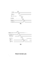
- FIG. 2 is a waveform diagram of the driving signal of the scanning line shown in FIG. 1.
- each pixel is connected to a scan line (such as GATE_N, GATE_N+1, GATE_N+2).
- the drive waveform of the scan line is shown in Figure 2.
- the scan lines are sequentially turned on, and the waveform of each scan line is shown.
- the width is approximately 10-20us.
- the connection between the scan line and the pixel is as shown in FIG. 3, and each pixel in the figure is connected to two scan lines, one of which scans the pixel.
- the charging voltage is referred to herein as the first type of scanning line, such as GATE_N, GATE_N+1, and GATE_N+2; the other scanning line controls the charge sharing of the sub-pixels of the pixel, which is referred to herein as the second type of scanning line, such as SHARING_N. , SHARING_N+1, SHARING_N+2.
- the first type of scan line is the nth scan line (such as GATE_N)
- the second type of scan line is the n+1th scan line (such as SHARING_N), where SHARING_N is the next scan line of GATE_N.
- the second type of scan line is the n+2 A scan line (such as SHARING_N), where SHARING_N is the next two scan lines of GATE_N.
- the second type of scan line can also be the n+mth scan line (m is a positive integer greater than 2).
- Fig. 5 is a driving waveform diagram of a scanning line of a liquid crystal display device having a multi-region design.
- the first type of scan lines GATE_N, GATE_N+1, GATE_N+2
- the second type of scan lines SHARING_N, SHARING_N+1, SHARING_N+2 are sequentially opened, each scan The line has a waveform width of 10-20us.
- the sub-pixels can work normally, and the opening time of the second type of scanning lines must be later than the opening time of the first type of scanning lines.
- the driving waveform of the scanning line is as shown in FIG. 6.
- the opening time of the second type of scanning line is earlier than the opening time of the first type of scanning line.
- the multi-zone design of the liquid crystal display should have the driving effect.
- An object of the present invention is to provide a reverse scanning liquid crystal display device and a driving method thereof without increasing the cost. In order to solve the technical problem that the conventional liquid crystal display device cannot maintain the proper driving effect when the reverse scanning drive is employed.
- the present invention provides a liquid crystal display device including: a scan driving module for generating a first scan signal; a data driving module for generating a gray scale signal; and a pixel for displaying the gray according to the first scan signal a signal, each pixel comprising at least two sub-pixels and a pixel capacitance that redistributes the gray signal of the sub-pixel; a data line, respectively connected to the data driving module and the pixel, for controlling a charging voltage of the pixel according to the gray signal; a shift register module, configured to generate a second scan signal corresponding to the first scan signal according to the first scan signal; and a scan line, including: a first type of scan line, and the scan drive module and the a pixel connection for controlling a charging time of the pixel according to the first scan signal; and a second type of scan line connected to the pixel, configured to control a sub-pixel of the pixel according to the second scan signal Driving time; the shift register module is respectively connected to the first type of scan line and the second type of
- the present invention relates to a liquid crystal display device, comprising: a scan driving module for generating a first scan signal; a data driving module for generating a gray scale signal; and a pixel for displaying the gray light according to the first scan signal a signal, each pixel comprising at least two sub-pixels and a pixel capacitance for reallocating a gray signal of the sub-pixel; a data line: respectively connected to the data driving module and the pixel, for The level signal controls a charging voltage of the pixel; a shift registering module: configured to generate a second scan signal corresponding to the first scan signal according to the first scan signal; and a scan line: comprising: a first type of scan line Connecting to the scan driving module and the pixel, respectively, for controlling a charging time of the pixel according to the first scanning signal; and a second type of scanning line: connecting with the pixel, according to the first a second scan signal controlling a driving time of the sub-pixels of the pixel; the shift register module is respectively associated with the
- the first type of scan lines and the second type of scan lines are spaced apart, and the first type of scan lines and the corresponding second type of scan lines are spaced apart by A scan lines.
- A is a positive integer greater than zero.
- the time at which the shift register module receives the first scan signal is t
- the time at which the shift register module generates the second scan signal corresponding to the first scan signal is t+T, where T is the predetermined delay time.
- the shift register module is a single shift register, and the shift register includes a signal input pin, a clock input pin, an output pin, and a feedback pin, and the signal input tube
- the pin is connected to the first type of scan line, and the output pin and the feedback pin are respectively connected to the second type of scan line, and the clock input pin is used to input the predetermined delay time T.
- the shift register module includes a plurality of shift registers serially connected in series, the shift register including a signal input pin, a clock input pin, an output pin, and a feedback tube.
- the signal input pin is connected to an output pin of a shift register of a previous stage, and the output pin is respectively connected to a signal input pin of a shift register of a next stage and a shift register of a previous stage a feedback pin connection
- the clock input pin is configured to input the predetermined delay time T;
- a signal input pin of the shift register of the first stage is connected to the first type of scan line, and a shift register of the last stage
- the output pins are respectively connected to the second type of scan line connection and the feedback pin of the shift register of the previous stage.
- the waveform width of the first scan signal and the second scan signal is 10-20 us.
- the present invention also relates to a driving method of a liquid crystal display device, wherein the liquid crystal display device comprises: a scan driving module, a shift register module, and a scan line, comprising: a first type of scan line for controlling a charging time of the pixel; a second type of scan line for controlling the driving time of the sub-pixels of the pixel; when the liquid crystal display device scans, the steps include the following steps: S10, the scan driving module generates a first scan signal to drive the first class a scan line; S20, the shift register module generates a second scan signal corresponding to the first scan signal according to the first scan signal; S30, driving and the first type of scan according to the second scan signal The corresponding second type of scan line for the line.
- the time at which the shift register module receives the first scan signal is t, and the shift register module generates a second scan signal corresponding to the first scan signal.
- the time is t+T, where T is the predetermined delay time.
- the first type of scanning lines and the second type of scanning lines are spaced apart, and the first type of scanning lines and the corresponding second type of scanning lines are spaced apart by A Scan line, where A is a positive integer greater than zero.
- the shift register module is a single shift register, and the shift register includes a signal input pin, a clock input pin, an output pin, and a feedback pin, a signal input pin is connected to the first type of scan line, the output pin and the feedback pin are respectively connected to the second type of scan line, and the clock input pin is used to input the predetermined delay time T.
- the shift register module includes a plurality of shift registers serially connected in series, the shift register including a signal input pin, a clock input pin, and an output pin. And a feedback pin, wherein the signal input pin is connected to an output pin of the shift register of the upper stage, and the output pin is respectively shifted from the signal input pin of the shift register of the next stage and the upper stage a feedback pin of the bit register is connected, the clock input pin is for inputting the predetermined delay time T; a signal input pin of the shift register of the first stage is connected to the first type of scan line, and the last stage is The output pins of the shift register are respectively connected to the second type of scan line connection and the feedback pin of the shift register of the previous stage.
- the waveform width of the first scan signal and the second scan signal is 10-20 us.
- the liquid crystal display device and the driving method thereof can realize reverse scanning of any liquid crystal display device without increasing device cost, and solve the technology that the existing liquid crystal display device cannot maintain the proper driving effect when using reverse scanning driving. problem.
- FIG. 1 is a schematic structural view of a scanning line and a pixel of a conventional liquid crystal display device
- FIG. 2 is a waveform diagram of driving signals of the scanning line shown in FIG. 1;
- FIG. 3 is a schematic structural view of a scanning line and a pixel of a liquid crystal display device of a conventional multi-region design
- FIG. 4 is a second schematic structural view of a scanning line and a pixel of a liquid crystal display device of a multi-region design
- FIG. 5 is a waveform diagram of driving signals of scan lines of a liquid crystal display device of a conventional multi-region design
- FIG. 6 is a waveform diagram of driving signals of scan lines in a reverse scanning of a conventional multi-region design liquid crystal display device
- FIG. 7 is a schematic structural view of a scanning line and a pixel of a liquid crystal display device of the present invention.
- FIG. 8 is a schematic structural view of a single shift register of a liquid crystal display device of the present invention.
- FIG. 9 is a schematic diagram showing the connection of a plurality of shift registers of the liquid crystal display device of the present invention.
- FIG. 10 is a second schematic structural view of a scanning line and a pixel of a liquid crystal display device of the present invention.
- the liquid crystal display device includes a scan driving module 710, a data driving module (not shown), a pixel 720, and a data line 730.
- the scan driver module 710 is configured to generate a first scan signal.
- the data drive module is used to generate grayscale signals.
- the pixel 720 is configured to display a gray signal according to the first scan signal, and each of the pixels 720 includes at least two sub-pixels and a pixel capacitance for reallocating the gray signal of the sub-pixel.
- Data lines 730 are coupled to data drive modules and pixels 720, respectively, for controlling the charging voltage of the pixels based on the gray scale signals.
- the shift register module 740 is configured to generate a second scan signal corresponding to the first scan signal according to the first scan signal (wherein the waveform width of the first scan signal and the second scan signal is preferably 10-20 us).
- the scan line 750 includes a first type of scan lines (GATE_N, GATE_N+1, GATE_N+2) and a second type of scan lines (SHARING_N, SHARING_N+1, SHARING_N+2), and the first type of scan lines are respectively associated with the scan driving module 710 and
- the pixel 720 is connected for controlling the charging time of the pixel 720 according to the first scan signal;
- the second type of scan line is respectively connected to the shift register module 740 and the pixel 720 for controlling the driving of the sub-pixel of the pixel 720 according to the second scan signal. time.
- the first type of scan lines are connected to the corresponding second type of scan lines by a shift register module 740.
- the liquid crystal display device of the present invention connects the first type of scan lines and the second type of scan lines corresponding to the first type of scan lines through the shift register module 740 (the second type of scan lines are connected to the corresponding first type of scan lines) The same pixel 720).
- a predetermined delay time T is first set in the shift register module 740, and the first scan signal of the first type of scan line (such as GATE_N) is received by the shift register module 740 (assuming that the time is t), at this time, the first type of scan line charges the pixel 720 according to the first scan signal and the gray signal (where the first scan signal controls the charging time, the gray signal controls the charging voltage); and the shift register module 740 After delaying the predetermined delay time T (time t+T), generating a second scan signal corresponding to the first scan signal, and transmitting the second scan signal to the second type of scan line corresponding to the first type of scan line (such as SHARING_N), at this time, since the corresponding pixel 720 has completed the charging operation, the second type of scanning line drives the sub-pixel according to the second scanning signal and the pixel capacitance (where the second scanning signal controls the driving time, the pixel capacitance control) Grayscale signal size of different sub-pixels
- the second scan signal in the second type of scan line is always later than the first scan signal in the corresponding first type of scan line by a predetermined delay time T. Therefore, when the liquid crystal display device of the present invention adopts reverse scanning, it is also ensured that the turn-on time of the second type of scan lines is later than the turn-on time of the corresponding first type of scan lines, and the delay time can be changed by changing the predetermined delay time T Make adjustments so that they are exactly the same as when scanning forward. Under this design, the liquid crystal display device of the present invention realizes the reverse scanning function of the liquid crystal display device by adding a shift register module 740 to the existing liquid crystal display device, thereby increasing the competitiveness of the product.
- FIG. 8 is a schematic structural diagram of a single shift register of the liquid crystal display device of the present invention.
- the shift register module is a single shift register, and the shift register includes a signal input pin Input and a clock input pin CLK.
- the output pin Out and the feedback pin FB wherein the signal input pin Input is connected to the first type of scan line, the output pin Output and the feedback pin FB are respectively connected to the second type scan line, and the clock input pin CLK is used. Enter the predetermined delay time T.
- the signal input pin Input receives the first scan signal of the first type of scan line as a trigger, and at this time, the input end of the signal input pin is at a high level, so that the potential of the Q point rises, and then turns on.
- T1 causes the output pin Output to output the CLK signal, at which time CLK is low.
- the first scan signal is off, the input terminal of the signal input pin is low, so that T2 is turned off, but the potential of Q is still high, then CLK is high, so the output pin Output is output high.
- the second scan signal is played.
- the feedback pin FB receives the high level signal of the second type of scan line after a certain delay, turns on T3 and T4, pulls the potentials of the output pin Output and Q point low, and then closes the output of the output pin Output, thereby A duty cycle of the shift register is completed.
- the shift register module includes a plurality of shift registers serially connected in series to a plurality of stages, the shift register including signals The input pin ST, the clock input pin CLK, the output pin Out, and the feedback pin FB, the signal input pin ST is connected to the output pin Out of the shift register of the previous stage, and the output pin Out is respectively separated from the next stage.
- the signal input pin ST of the shift register is connected to the feedback pin FB of the shift register of the previous stage, and the clock input pin CLK is used to input the predetermined delay time T; the shift register of the first stage
- the signal input pin ST is connected to the first type of scan line, and the output pin Out of the shift register of the last stage is respectively connected to the second type of scan line and the feedback pin FB of the shift register of the previous stage. connection.
- a better and more precise adjustment of the predetermined delay time T can be achieved by using the above-described plurality of shift registers connected in series. The operation of a single shift register is the same as described above.
- the first type of scanning lines GATE_N, GATE_N+1, GATE_N+2
- the second type of scan lines SHARING_N, SHARING_N+1, SHARING_N+2 are arranged at intervals, and the scan lines of the first type and the corresponding scan lines of the second type are separated by A scan lines, wherein A is a positive integer greater than 0.
- a shown in FIG. 10 is 2, and of course, other positive integers greater than 0 may be used.
- the liquid crystal display device of the present invention can be modified and implemented on a liquid crystal display device of any existing multi-region design, and only the first type of scan lines and the corresponding second type of scan lines need to be connected by using a shift register module.
- the present invention also relates to a driving method of a liquid crystal display device, wherein the liquid crystal display device comprises: a scan driving module, a shift register module, and a scan line: comprising: a first type of scan line for controlling charging time of the pixel; Class scan line: The drive time for controlling the sub-pixels of the pixel.
- the steps include the following steps: S10, the scan driving module generates a first scan signal to drive the first type of scan lines; S20, the shift register module generates according to the first scan signal. a second scan signal corresponding to the first scan signal; S30, driving a second type of scan line corresponding to the first type of scan line according to the second scan signal.
- the time when the shift register module receives the first scan signal is t, and the time when the shift register module generates the second scan signal corresponding to the first scan signal is t+T, where T is a predetermined delay.
- the second scan signal of the second type of scan line in the driving method of the liquid crystal display device of the present invention can be fixedly delayed by the corresponding first scan signal time T, thereby ensuring the normal display effect when the liquid crystal display device is driven in the forward direction, that is, the first The two scan signals are not activated earlier than the corresponding first scan signal.
Landscapes
- Physics & Mathematics (AREA)
- Nonlinear Science (AREA)
- Geometry (AREA)
- Mathematical Physics (AREA)
- Chemical & Material Sciences (AREA)
- Crystallography & Structural Chemistry (AREA)
- General Physics & Mathematics (AREA)
- Optics & Photonics (AREA)
- Control Of Indicators Other Than Cathode Ray Tubes (AREA)
- Liquid Crystal Display Device Control (AREA)
Abstract
一种液晶显示装置及其驱动方法,其中液晶显示装置包括扫描驱动模块(710)、数据驱动模块、像素(720)、数据线(730)、移位寄存模块(740)以及扫描线(750),扫描线(750)包括第一类扫描线(GATE_N)与第二类扫描线(SHARING_N),第一类扫描线(GATE_N)与扫描驱动模块(710)和像素(720)连接,用于根据第一扫描信号控制像素(720)的充电时间;第二类扫描线(SHARING_N)与移位寄存模块(740)和像素(720)连接,用于根据第二扫描信号控制像素(720)的子像素的驱动时间。不用增加装置成本即可实现反向扫描,解决了现有的液晶显示装置在采用反向扫描驱动时无法保持应有的驱动效果的技术问题。
Description
本发明涉及液晶显示领域,特别是涉及一种不增加成本即可实现反向扫描的液晶显示装置及其驱动方法。
现在的液晶显示装置一般采用图1所示的扫描线与像素之间连接方式进行驱动,图2为图1所示的扫描线的驱动信号波形图。如图1所示,每个像素连接到一条扫描线(如GATE_N、GATE_N+1、GATE_N+2),扫描线的驱动波形如图2所示,扫描线依序打开,每条扫描线的波形宽度大约为10-20us。
当液晶显示装置具有多区域(multi-domain)设计时,扫描线与像素之间的连接方式如图3所示,图中每个像素都连接到两条扫描线上,其中一条扫描线控制像素充电的电压,这里称其为第一类扫描线,如GATE_N、GATE_N+1、GATE_N+2;另一条扫描线控制像素的子像素的电荷共享,这里称其为第二类扫描线,如SHARING_N、SHARING_N+1、SHARING_N+2。图中第一类扫描线为第n条扫描线(如GATE_N),第二类扫描线为第n+1条扫描线(如SHARING_N),其中SHARING_N为GATE_N的下一条扫描线。
图4为图3所示的扫描线与像素之间的连接方式的变形,不同之处为第一类扫描线为第n条扫描线(如GATE_N),第二类扫描线为第n+2条扫描线(如SHARING_N),其中SHARING_N为GATE_N的下两条扫描线。依次类推,第二类扫描线也可以为第n+m条扫描线(m为大于2的正整数)。
图5所示的为具有多区域设计的液晶显示装置的扫描线的驱动波形图。从图中可以看到,第一类扫描线(GATE_N、GATE_N+1、GATE_N+2)和第二类扫描线(SHARING_N、SHARING_N+1、SHARING_N+2)都是依序打开的,每条扫描线的波形宽度均为10-20us。为了满足多区域设计的应有效果,使得子像素可以正常的工作,第二类扫描线的打开时间必须晚于第一类扫描线的打开时间。但是这样的设计在显示器采用反向扫描的驱动时,其扫描线的驱动波形图如图6所示,第二类扫描线的打开时间就会早于第一类扫描线的打开时间造成无法保持多区域设计的液晶显示器应有的驱动效果。
故,有必要提供一种液晶显示装置及其驱动方法,以解决现有技术所存在的问题。
本发明的目的在于提供一种不增加成本即可实现反向扫描液晶显示装置及其驱动方法 ,
以解决现有的液晶显示装置在采用反向扫描驱动时无法保持应有的驱动效果的技术问题。
本发明设计一种液晶显示装置,其中包括:扫描驱动模块,用于产生第一扫描信号;数据驱动模块,用于产生灰度信号;像素,用于根据所述第一扫描信号显示所述灰度信号,每个像素包括至少两个子像素和对所述子像素的灰度信号进行重新分配的像素电容;
数据线,分别与所述数据驱动模块和所述像素连接,用于根据所述灰度信号控制所述像素的充电电压;
移位寄存模块,用于根据所述第一扫描信号产生与所述第一扫描信号相应的第二扫描信号;以及扫描线,包括:第一类扫描线,分别与所述扫描驱动模块和所述像素连接,用于根据所述第一扫描信号控制所述像素的充电时间;以及第二类扫描线,与所述像素连接,用于根据所述第二扫描信号控制所述像素的子像素的驱动时间;所述移位寄存模块分别与所述第一类扫描线以及与所述第一类扫描线相应的第二类扫描线连接;所述第一类扫描线和所述第二类扫描线间隔排列,所述第一类扫描线和相应的第二类扫描线之间间隔A条扫描线,其中A为大于0的正整数;所述移位寄存模块接收所述第一扫描信号的时间为t,所述移位寄存模块产生与所述第一扫描信号相应的第二扫描信号的时间为t+T,其中T为预定延迟时间。
本发明涉及一种液晶显示装置,其中包括:扫描驱动模块,用于产生第一扫描信号;数据驱动模块,用于产生灰度信号;像素:用于根据所述第一扫描信号显示所述灰度信号,每个像素包括至少两个子像素和对所述子像素的灰度信号进行重新分配的像素电容;数据线:分别与所述数据驱动模块和所述像素连接,用于根据所述灰度信号控制所述像素的充电电压;移位寄存模块:用于根据所述第一扫描信号产生与所述第一扫描信号相应的第二扫描信号;以及扫描线:包括:第一类扫描线:分别与所述扫描驱动模块和所述像素连接,用于根据所述第一扫描信号控制所述像素的充电时间;以及第二类扫描线:与所述像素连接,用于根据所述第二扫描信号控制所述像素的子像素的驱动时间;所述移位寄存模块分别与所述第一类扫描线以及与所述第一类扫描线相应的第二类扫描线连接。
在本发明的液晶显示装置中,所述第一类扫描线和所述第二类扫描线间隔排列,所述第一类扫描线和相应的第二类扫描线之间间隔A条扫描线,其中A为大于0的正整数。
在本发明的液晶显示装置中,所述移位寄存模块接收所述第一扫描信号的时间为t,所述移位寄存模块产生与所述第一扫描信号相应的第二扫描信号的时间为t+T,其中T为预定延迟时间。
在本发明的液晶显示装置中,所述移位寄存模块为单一移位寄存器,所述移位寄存器包括信号输入管脚、时钟输入管脚、输出管脚以及反馈管脚,所述信号输入管脚与所述第一类扫描线连接,所述输出管脚和所述反馈管脚分别与所述第二类扫描线连接,所述时钟输入管脚用于输入所述预定延迟时间T。
在本发明的液晶显示装置中,所述移位寄存模块包括依次串联成多级的多个移位寄存器,所述移位寄存器包括信号输入管脚、时钟输入管脚、输出管脚以及反馈管脚,所述信号输入管脚与上一级的移位寄存器的输出管脚连接,所述输出管脚分别与下一级的移位寄存器的信号输入管脚和上一级的移位寄存器的反馈管脚连接,所述时钟输入管脚用于输入所述预定延迟时间T;第一级的移位寄存器的信号输入管脚与所述第一类扫描线连接,最后一级的移位寄存器的输出管脚分别与所述第二类扫描线连接和上一级的移位寄存器的反馈管脚连接。
在本发明的液晶显示装置中,所述第一扫描信号和所述第二扫描信号的波形宽度为10-20us。
本发明还涉及一种液晶显示装置的驱动方法,其中所述液晶显示装置包括:扫描驱动模块,移位寄存模块,以及扫描线,包括:第一类扫描线,用于控制像素的充电时间;第二类扫描线,用于控制所述像素的子像素的驱动时间;当所述液晶显示装置扫描时,包括步骤如下:S10、所述扫描驱动模块产生第一扫描信号驱动所述第一类扫描线;S20、所述移位寄存模块根据所述第一扫描信号产生与所述第一扫描信号相应的第二扫描信号;S30、根据所述第二扫描信号驱动与所述第一类扫描线相应的第二类扫描线。
在本发明的液晶显示装置的驱动方法中,所述移位寄存模块接收所述第一扫描信号的时间为t,所述移位寄存模块产生与所述第一扫描信号相应的第二扫描信号的时间为t+T,其中T为预定延迟时间。
在本发明的液晶显示装置的驱动方法中,所述第一类扫描线和所述第二类扫描线间隔排列,所述第一类扫描线和相应的第二类扫描线之间间隔A条扫描线,其中A为大于0的正整数。
在本发明的液晶显示装置的驱动方法中,所述移位寄存模块为单一移位寄存器,所述移位寄存器包括信号输入管脚、时钟输入管脚、输出管脚以及反馈管脚,所述信号输入管脚与所述第一类扫描线连接,所述输出管脚和所述反馈管脚分别与所述第二类扫描线连接,所述时钟输入管脚用于输入所述预定延迟时间T。
在本发明的液晶显示装置的驱动方法中,所述移位寄存模块包括依次串联成多级的多个移位寄存器,所述移位寄存器包括信号输入管脚、时钟输入管脚、输出管脚以及反馈管脚,所述信号输入管脚与上一级的移位寄存器的输出管脚连接,所述输出管脚分别与下一级的移位寄存器的信号输入管脚和上一级的移位寄存器的反馈管脚连接,所述时钟输入管脚用于输入所述预定延迟时间T;第一级的移位寄存器的信号输入管脚与所述第一类扫描线连接,最后一级的移位寄存器的输出管脚分别与所述第二类扫描线连接和上一级的移位寄存器的反馈管脚连接。
在本发明的液晶显示装置的驱动方法中,所述第一扫描信号和所述第二扫描信号的波形宽度为10-20us。
本发明的液晶显示装置及其驱动方法不用增加装置成本即可实现任何液晶显示装置的反向扫描,解决了现有的液晶显示装置在采用反向扫描驱动时无法保持应有的驱动效果的技术问题。
图1为现有的液晶显示装置的扫描线和像素的结构示意图;
图2为图1所示扫描线的驱动信号波形图;
图3为现有的多区域设计的液晶显示装置的扫描线和像素的结构示意图之一;
图4为现有的多区域设计的液晶显示装置的扫描线和像素的结构示意图之二;
图5为现有的多区域设计的液晶显示装置的扫描线的驱动信号波形图;
图6为现有的多区域设计的液晶显示装置反向扫描时的扫描线的驱动信号波形图;
图7为本发明的液晶显示装置的扫描线和像素的结构示意图之一;
图8为本发明的液晶显示装置的单一移位寄存器的结构示意图;
图9为本发明的液晶显示装置的多个移位寄存器的连接示意图;
图10为本发明的液晶显示装置的扫描线和像素的结构示意图之二。
以下各实施例的说明是参考附加的图式,用以例示本发明可用以实施的特定实施例。本发明所提到的方向用语,例如「上」、「下」、「前」、「后」、「左」、「右」、「内」、「外」、「侧面」等,仅是参考附加图式的方向。因此,使用的方向用语是用以说明及理解本发明,而非用以限制本发明。
在图中,结构相似的单元是以相同标号表示。
在图7所示的本发明的液晶显示装置的扫描线和像素的结构示意图中,所述液晶显示装置包括扫描驱动模块710、数据驱动模块(图中未示出)、像素720、数据线730、移位寄存模块740以及扫描线750。扫描驱动模块710用于产生第一扫描信号。数据驱动模块用于产生灰度信号。像素720用于根据第一扫描信号显示灰度信号,每个像素720均包括至少两个子像素以及对子像素的灰度信号进行重新分配的像素电容。数据线730分别与数据驱动模块和像素720连接,用于根据灰度信号控制像素的充电电压。移位寄存模块740用于根据第一扫描信号产生与第一扫描信号相应的第二扫描信号(其中第一扫描信号和第二扫描信号的波形宽度优选为10-20us)。扫描线750包括第一类扫描线(GATE_N、GATE_N+1、GATE_N+2)以及第二类扫描线(SHARING_N、SHARING_N+1、SHARING_N+2),第一类扫描线分别与扫描驱动模块710和像素720连接,用于根据第一扫描信号控制像素720的充电时间;第二类扫描线分别与移位寄存模块740和像素720连接,用于根据第二扫描信号控制像素720的子像素的驱动时间。第一类扫描线通过移位寄存模块740与相应的第二类扫描线连接。
本发明的液晶显示装置通过移位寄存模块740将第一类扫描线以及与第一类扫描线相应的第二类扫描线连接(该第二类扫描线与相应的第一类扫描线连接到同一像素720)。本发明的液晶显示装置使用时,首先在移位寄存模块740中设定预定延迟时间T,当移位寄存模块740接收到第一类扫描线(如GATE_N)的第一扫描信号(假设时间为t),这时第一类扫描线根据第一扫描信号和灰度信号对像素720进行充电操作(其中第一扫描信号控制充电时间,灰度信号控制充电电压);同时移位寄存模块740会在延迟预定延迟时间T后(时间为t+T)产生一个与第一扫描信号相应的第二扫描信号,并把该第二扫描信号发送给与第一类扫描线相应的第二类扫描线(如SHARING_N),这时由于相应的像素720已经完成了充电操作,第二类扫描线根据第二扫描信号和像素电容对子像素进行驱动操作(其中第二扫描信号控制驱动时间,像素电容控制不同子像素的灰度信号大小)。
上述可见,第二类扫描线中的第二扫描信号始终晚于相应的第一类扫描线中的第一扫描信号预定延迟时间T。因此本发明的液晶显示装置在采用反向扫描时,同样可以确保第二类扫描线的开启时间晚于相应的第一类扫描线的开启时间,并且对于延迟的时间可以通过改变预定延迟时间T进行调整,这样和正向扫描时是完全一样的。在这种设计下,本发明的液晶显示装置仅通过在现有的液晶显示装置上增加一移位寄存模块740就实现了液晶显示装置的反向扫描功能,增加了产品的竞争力。
在图8所示本发明的液晶显示装置的单一移位寄存器的结构示意图,图中可见移位寄存模块为单一移位寄存器,所述移位寄存器包括信号输入管脚Input、时钟输入管脚CLK、输出管脚Out以及反馈管脚FB,其中信号输入管脚Input与第一类扫描线连接,输出管脚Output与反馈管脚FB分别与第二类扫描线连接,时钟输入管脚CLK用于输入预定延迟时间T。本移位寄存器工作时,信号输入管脚Input接收到第一类扫描线的第一扫描信号作为触发,这时信号输入管脚Input端为高电平,使得Q点的电位升高,进而打开T1,使得输出管脚Output输出CLK信号,这时CLK为低电平。当第一扫描信号关闭时,信号输入管脚Input端为低电平,使得T2关闭,但是Q点电位依然保持高电平,这时CLK为高电平,于是输出管脚Output输出高电平打出第二扫描信号。同时反馈管脚FB在一定延迟后接收到第二类扫描线的高电平信号,开启T3和T4,将输出管脚Output和Q点的电位拉低,进而关闭输出管脚Output的输出,从而完成了移位寄存器的一个工作周期。
在图9所示的本发明的液晶显示装置的多个移位寄存器的连接示意图中,图中可见移位寄存模块包括依次串联成多级的多个移位寄存器,所述移位寄存器包括信号输入管脚ST、时钟输入管脚CLK、输出管脚Out以及反馈管脚FB,信号输入管脚ST与上一级的移位寄存器的输出管脚Out连接,输出管脚Out分别与下一级的移位寄存器的信号输入管脚ST和上一级的移位寄存器的反馈管脚FB连接,所述时钟输入管脚CLK用于输入所述预定延迟时间T;第一级的移位寄存器的信号输入管脚ST与所述第一类扫描线连接,最后一级的移位寄存器的输出管脚Out分别与所述第二类扫描线连接和上一级的移位寄存器的反馈管脚FB连接。采用上述的串联成多级的多个移位寄存器可以对预定延迟时间T进行更好、更精确的调整。单一的移位寄存器的工作原理与上述的相同。
作为本发明的液晶显示装置的优选实施例,如图10所示的本发明的液晶显示装置的扫描线和像素的结构示意图中,第一类扫描线(GATE_N、GATE_N+1、GATE_N+2)和第二类扫描线(SHARING_N、SHARING_N+1、SHARING_N+2)间隔排列,第一类扫描线和相应的第二类扫描线之间间隔A条扫描线,其中A为大于0的正整数,其中图10所示的A为2,当然也可为其他的大于0的正整数。本发明的液晶显示装置可以在现有的任意多区域设计的液晶显示装置上进行改造实现,只需要将第一类扫描线和相应的第二类扫描线使用移位寄存模块连接即可。
本发明还涉及一种液晶显示装置的驱动方法,其中液晶显示装置包括:扫描驱动模块,移位寄存模块,以及扫描线:包括:第一类扫描线,用于控制像素的充电时间;第二类扫描线:用于控制所述像素的子像素的驱动时间。当所述液晶显示装置扫描时,包括步骤如下:S10、所述扫描驱动模块产生第一扫描信号驱动所述第一类扫描线;S20、所述移位寄存模块根据所述第一扫描信号产生与所述第一扫描信号相应的第二扫描信号;S30、根据所述第二扫描信号驱动与所述第一类扫描线相应的第二类扫描线。
其中所述移位寄存模块接收所述第一扫描信号的时间为t,所述移位寄存模块产生与所述第一扫描信号相应的第二扫描信号的时间为t+T,其中T为预定延迟时间。
本发明的液晶显示装置的驱动方法中的第二类扫描线的第二扫描信号可固定延迟于相应的第一扫描信号时间T,保证了液晶显示装置正向驱动时的正常显示效果,即第二扫描信号不会早于相应的第一扫描信号启动。
综上所述,虽然本发明已以优选实施例揭露如上,但上述优选实施例并非用以限制本发明,本领域的普通技术人员,在不脱离本发明的精神和范围内,均可作各种更动与润饰,因此本发明的保护范围以权利要求界定的范围为准。
Claims (15)
- 一种液晶显示装置,其特征在于,包括:扫描驱动模块,用于产生第一扫描信号;数据驱动模块,用于产生灰度信号;像素,用于根据所述第一扫描信号显示所述灰度信号,每个像素包括至少两个子像素和对所述子像素的灰度信号进行重新分配的像素电容;数据线,分别与所述数据驱动模块和所述像素连接,用于根据所述灰度信号控制所述像素的充电电压;移位寄存模块,用于根据所述第一扫描信号产生与所述第一扫描信号相应的第二扫描信号;以及扫描线,包括:第一类扫描线,分别与所述扫描驱动模块和所述像素连接,用于根据所述第一扫描信号控制所述像素的充电时间;以及第二类扫描线,与所述像素连接,用于根据所述第二扫描信号控制所述像素的子像素的驱动时间;所述移位寄存模块分别与所述第一类扫描线以及与所述第一类扫描线相应的第二类扫描线连接;所述第一类扫描线和所述第二类扫描线间隔排列,所述第一类扫描线和相应的第二类扫描线之间间隔A条扫描线,其中A为大于0的正整数;所述移位寄存模块接收所述第一扫描信号的时间为t,所述移位寄存模块产生与所述第一扫描信号相应的第二扫描信号的时间为t+T,其中T为预定延迟时间。
- 一种液晶显示装置,其特征在于,包括:扫描驱动模块,用于产生第一扫描信号;数据驱动模块,用于产生灰度信号;像素,用于根据所述第一扫描信号显示所述灰度信号,每个像素包括至少两个子像素和对所述子像素的灰度信号进行重新分配的像素电容;数据线,分别与所述数据驱动模块和所述像素连接,用于根据所述灰度信号控制所述像素的充电电压;移位寄存模块,用于根据所述第一扫描信号产生与所述第一扫描信号相应的第二扫描信号;以及扫描线,包括:第一类扫描线,分别与所述扫描驱动模块和所述像素连接,用于根据所述第一扫描信号控制所述像素的充电时间;以及第二类扫描线,与所述像素连接,用于根据所述第二扫描信号控制所述像素的子像素的驱动时间;所述移位寄存模块分别与所述第一类扫描线以及与所述第一类扫描线相应的第二类扫描线连接。
- 根据权利要求2所述的液晶显示装置,其特征在于,所述第一类扫描线和所述第二类扫描线间隔排列,所述第一类扫描线和相应的第二类扫描线之间间隔A条扫描线,其中A为大于0的正整数。
- 根据权利要求2所述的液晶显示装置,其特征在于,所述移位寄存模块接收所述第一扫描信号的时间为t,所述移位寄存模块产生与所述第一扫描信号相应的第二扫描信号的时间为t+T,其中T为预定延迟时间。
- 根据权利要求4所述的液晶显示装置,其特征在于,所述移位寄存模块为单一移位寄存器,所述移位寄存器包括信号输入管脚、时钟输入管脚、输出管脚以及反馈管脚,所述信号输入管脚与所述第一类扫描线连接,所述输出管脚和所述反馈管脚分别与所述第二类扫描线连接,所述时钟输入管脚用于输入所述预定延迟时间T。
- 根据权利要求4所述的液晶显示装置,其特征在于,所述移位寄存模块包括依次串联成多级的多个移位寄存器,所述移位寄存器包括信号输入管脚、时钟输入管脚、输出管脚以及反馈管脚,所述信号输入管脚与上一级的移位寄存器的输出管脚连接,所述输出管脚分别与下一级的移位寄存器的信号输入管脚和上一级的移位寄存器的反馈管脚连接,所述时钟输入管脚用于输入所述预定延迟时间T;第一级的移位寄存器的信号输入管脚与所述第一类扫描线连接,最后一级的移位寄存器的输出管脚分别与所述第二类扫描线连接和上一级的移位寄存器的反馈管脚连接。
- 根据权利要求2所述的液晶显示装置,其特征在于,所述第一扫描信号和所述第二扫描信号的波形宽度为10-20us。
- 一种液晶显示装置的驱动方法,其特征在于,所述液晶显示装置包括:扫描驱动模块,移位寄存模块,以及扫描线,包括:第一类扫描线,用于控制像素的充电时间;第二类扫描线,用于控制所述像素的子像素的驱动时间;当所述液晶显示装置扫描时,包括步骤如下:S10、所述扫描驱动模块产生第一扫描信号驱动所述第一类扫描线;S20、所述移位寄存模块根据所述第一扫描信号产生与所述第一扫描信号相应的第二扫描信号;S30、根据所述第二扫描信号驱动与所述第一类扫描线相应的第二类扫描线。
- 根据权利要求8所述的液晶显示装置的驱动方法,其特征在于,所述移位寄存模块接收所述第一扫描信号的时间为t,所述移位寄存模块产生与所述第一扫描信号相应的第二扫描信号的时间为t+T,其中T为预定延迟时间。
- 根据权利要求8所述的液晶显示装置的驱动方法,其特征在于,所述第一类扫描线和所述第二类扫描线间隔排列,所述第一类扫描线和相应的第二类扫描线之间间隔A条扫描线,其中A为大于0的正整数。
- 根据权利要求9所述的液晶显示装置的驱动方法,其特征在于,所述移位寄存模块为单一移位寄存器,所述移位寄存器包括信号输入管脚、时钟输入管脚、输出管脚以及反馈管脚,所述信号输入管脚与所述第一类扫描线连接,所述输出管脚和所述反馈管脚分别与所述第二类扫描线连接,所述时钟输入管脚用于输入所述预定延迟时间T。
- 根据权利要求9所述的液晶显示装置的驱动方法,其特征在于,所述移位寄存模块包括依次串联成多级的多个移位寄存器,所述移位寄存器包括信号输入管脚、时钟输入管脚、输出管脚以及反馈管脚,所述信号输入管脚与上一级的移位寄存器的输出管脚连接,所述输出管脚分别与下一级的移位寄存器的信号输入管脚和上一级的移位寄存器的反馈管脚连接,所述时钟输入管脚用于输入所述预定延迟时间T;第一级的移位寄存器的信号输入管脚与所述第一类扫描线连接,最后一级的移位寄存器的输出管脚分别与所述第二类扫描线连接和上一级的移位寄存器的反馈管脚连接。
- 根据权利要求10所述的液晶显示装置的驱动方法,其特征在于,所述移位寄存模块为单一移位寄存器,所述移位寄存器包括信号输入管脚、时钟输入管脚、输出管脚以及反馈管脚,所述信号输入管脚与所述第一类扫描线连接,所述输出管脚和所述反馈管脚分别与所述第二类扫描线连接,所述时钟输入管脚用于输入所述预定延迟时间T。
- 根据权利要求10所述的液晶显示装置的驱动方法,其特征在于,所述移位寄存模块包括依次串联成多级的多个移位寄存器,所述移位寄存器包括信号输入管脚、时钟输入管脚、输出管脚以及反馈管脚,所述信号输入管脚与上一级的移位寄存器的输出管脚连接,所述输出管脚分别与下一级的移位寄存器的信号输入管脚和上一级的移位寄存器的反馈管脚连接,所述时钟输入管脚用于输入所述预定延迟时间T;第一级的移位寄存器的信号输入管脚与所述第一类扫描线连接,最后一级的移位寄存器的输出管脚分别与所述第二类扫描线连接和上一级的移位寄存器的反馈管脚连接。
- 根据权利要求8所述的液晶显示装置的驱动方法,其特征在于,所述第一扫描信号和所述第二扫描信号的波形宽度为10-20us。
Priority Applications (1)
| Application Number | Priority Date | Filing Date | Title |
|---|---|---|---|
| US13/378,270 US8928707B2 (en) | 2011-09-27 | 2011-10-09 | Liquid crystal display device and driving method thereof |
Applications Claiming Priority (2)
| Application Number | Priority Date | Filing Date | Title |
|---|---|---|---|
| CN2011102977296A CN102324224B (zh) | 2011-09-27 | 2011-09-27 | 液晶显示装置及其驱动方法 |
| CN201110297729.6 | 2011-09-27 |
Publications (1)
| Publication Number | Publication Date |
|---|---|
| WO2013044527A1 true WO2013044527A1 (zh) | 2013-04-04 |
Family
ID=45451958
Family Applications (1)
| Application Number | Title | Priority Date | Filing Date |
|---|---|---|---|
| PCT/CN2011/080583 Ceased WO2013044527A1 (zh) | 2011-09-27 | 2011-10-09 | 液晶显示装置及其驱动方法 |
Country Status (2)
| Country | Link |
|---|---|
| CN (1) | CN102324224B (zh) |
| WO (1) | WO2013044527A1 (zh) |
Cited By (1)
| Publication number | Priority date | Publication date | Assignee | Title |
|---|---|---|---|---|
| CN106128384A (zh) * | 2016-08-25 | 2016-11-16 | 深圳市华星光电技术有限公司 | 栅极驱动装置以及显示面板 |
Families Citing this family (6)
| Publication number | Priority date | Publication date | Assignee | Title |
|---|---|---|---|---|
| CN102938245A (zh) * | 2012-11-22 | 2013-02-20 | 深圳市华星光电技术有限公司 | 液晶显示面板及液晶显示装置 |
| CN103943083B (zh) * | 2014-03-27 | 2017-02-15 | 京东方科技集团股份有限公司 | 一种栅极驱动电路及其驱动方法、显示装置 |
| CN103928010A (zh) * | 2014-05-04 | 2014-07-16 | 深圳市华星光电技术有限公司 | 用于驱动液晶面板的数据驱动电路及液晶面板的驱动方法 |
| CN105045009B (zh) * | 2015-08-24 | 2018-04-10 | 深圳市华星光电技术有限公司 | 一种液晶显示面板及其阵列基板 |
| CN105609077B (zh) * | 2016-01-28 | 2018-03-30 | 深圳市华星光电技术有限公司 | 像素驱动电路 |
| CN110033737B (zh) * | 2019-05-31 | 2021-10-26 | 上海天马有机发光显示技术有限公司 | 一种扫描电路、显示面板及显示装置 |
Citations (5)
| Publication number | Priority date | Publication date | Assignee | Title |
|---|---|---|---|---|
| CN101017265A (zh) * | 2007-03-12 | 2007-08-15 | 友达光电股份有限公司 | 像素控制装置及应用该像素控制装置的显示装置 |
| CN101364017A (zh) * | 2007-08-10 | 2009-02-11 | 群康科技(深圳)有限公司 | 薄膜晶体管基板及其制造方法、液晶显示装置及其驱动方法 |
| US20100157185A1 (en) * | 2008-12-18 | 2010-06-24 | Samsung Electronics Co., Ltd. | Liquid crystal display |
| CN101819365A (zh) * | 2009-11-13 | 2010-09-01 | 友达光电股份有限公司 | 液晶显示面板及其像素列的驱动方法 |
| TW201101279A (en) * | 2009-06-16 | 2011-01-01 | Au Optronics Corp | Liquid crystal display panel and pixel driving method thereof |
Family Cites Families (4)
| Publication number | Priority date | Publication date | Assignee | Title |
|---|---|---|---|---|
| EP1808844B1 (en) * | 2006-01-13 | 2012-10-31 | Semiconductor Energy Laboratory Co., Ltd. | Display device |
| KR20070121318A (ko) * | 2006-06-22 | 2007-12-27 | 삼성전자주식회사 | 액정표시장치 및 이의 구동방법 |
| CN201477335U (zh) * | 2009-05-14 | 2010-05-19 | 福建华映显示科技有限公司 | 液晶显示装置 |
| CN202258266U (zh) * | 2011-09-27 | 2012-05-30 | 深圳市华星光电技术有限公司 | 液晶显示装置 |
-
2011
- 2011-09-27 CN CN2011102977296A patent/CN102324224B/zh not_active Expired - Fee Related
- 2011-10-09 WO PCT/CN2011/080583 patent/WO2013044527A1/zh not_active Ceased
Patent Citations (5)
| Publication number | Priority date | Publication date | Assignee | Title |
|---|---|---|---|---|
| CN101017265A (zh) * | 2007-03-12 | 2007-08-15 | 友达光电股份有限公司 | 像素控制装置及应用该像素控制装置的显示装置 |
| CN101364017A (zh) * | 2007-08-10 | 2009-02-11 | 群康科技(深圳)有限公司 | 薄膜晶体管基板及其制造方法、液晶显示装置及其驱动方法 |
| US20100157185A1 (en) * | 2008-12-18 | 2010-06-24 | Samsung Electronics Co., Ltd. | Liquid crystal display |
| TW201101279A (en) * | 2009-06-16 | 2011-01-01 | Au Optronics Corp | Liquid crystal display panel and pixel driving method thereof |
| CN101819365A (zh) * | 2009-11-13 | 2010-09-01 | 友达光电股份有限公司 | 液晶显示面板及其像素列的驱动方法 |
Cited By (2)
| Publication number | Priority date | Publication date | Assignee | Title |
|---|---|---|---|---|
| CN106128384A (zh) * | 2016-08-25 | 2016-11-16 | 深圳市华星光电技术有限公司 | 栅极驱动装置以及显示面板 |
| CN106128384B (zh) * | 2016-08-25 | 2019-11-26 | 深圳市华星光电技术有限公司 | 栅极驱动装置以及显示面板 |
Also Published As
| Publication number | Publication date |
|---|---|
| CN102324224A (zh) | 2012-01-18 |
| CN102324224B (zh) | 2013-03-27 |
Similar Documents
| Publication | Publication Date | Title |
|---|---|---|
| EP3828875B1 (en) | Shift register unit and driving method therefor, gate driving circuit and display apparatus | |
| US10043477B2 (en) | GOA circuit | |
| WO2013044527A1 (zh) | 液晶显示装置及其驱动方法 | |
| US10262615B2 (en) | Shift register, driving method, and gate electrode drive circuit | |
| US10223993B2 (en) | Shift register and driving method thereof, gate driving circuit and display apparatus | |
| US10186221B2 (en) | Shift register, driving method thereof, gate driving circuit and display device | |
| US10019929B2 (en) | Gate drive circuit and display device using the same | |
| US9875709B2 (en) | GOA circuit for LTPS-TFT | |
| JP4713246B2 (ja) | 液晶表示素子 | |
| KR101157241B1 (ko) | 게이트 드라이버 및 그 구동 방법 | |
| CN103534747B (zh) | 扫描信号线驱动电路、显示装置以及扫描信号线的驱动方法 | |
| US20190156778A1 (en) | Shift register unit, gate driving circuit, and driving method | |
| US10049639B2 (en) | CMOS gate drive on array (GOA) circuit structure and liquid crystal display panel | |
| CN112309322B (zh) | 移位寄存器及其驱动方法、栅极驱动电路和显示装置 | |
| US10121442B2 (en) | Driving methods and driving devices of gate driver on array (GOA) circuit | |
| US20130235026A1 (en) | Scanning signal line drive circuit and display device equipped with same | |
| US20170309243A1 (en) | Shift register unit and driving method thereof, gate driving apparatus and display apparatus | |
| WO2016058352A1 (zh) | 栅极驱动电路、显示电路及驱动方法和显示装置 | |
| WO2019062287A1 (zh) | 移位寄存器单元、栅极驱动电路及驱动方法、显示装置 | |
| CN105810170A (zh) | 移位寄存器单元及其驱动方法、栅线驱动电路和阵列基板 | |
| KR20110102627A (ko) | 쉬프트 레지스터와 이를 이용한 표시장치 | |
| US11393402B2 (en) | OR logic operation circuit and driving method, shift register unit, gate drive circuit, and display device | |
| US20190103067A1 (en) | Gate driving circuit and display device using the same | |
| WO2017113447A1 (zh) | 栅极驱动电路及显示装置 | |
| US20180218686A1 (en) | Goa circuit |
Legal Events
| Date | Code | Title | Description |
|---|---|---|---|
| WWE | Wipo information: entry into national phase |
Ref document number: 13378270 Country of ref document: US |
|
| 121 | Ep: the epo has been informed by wipo that ep was designated in this application |
Ref document number: 11873470 Country of ref document: EP Kind code of ref document: A1 |
|
| NENP | Non-entry into the national phase |
Ref country code: DE |
|
| 122 | Ep: pct application non-entry in european phase |
Ref document number: 11873470 Country of ref document: EP Kind code of ref document: A1 |