WO2013021808A1 - 発光素子、面光源装置、表示装置および照明装置 - Google Patents
発光素子、面光源装置、表示装置および照明装置 Download PDFInfo
- Publication number
- WO2013021808A1 WO2013021808A1 PCT/JP2012/068640 JP2012068640W WO2013021808A1 WO 2013021808 A1 WO2013021808 A1 WO 2013021808A1 JP 2012068640 W JP2012068640 W JP 2012068640W WO 2013021808 A1 WO2013021808 A1 WO 2013021808A1
- Authority
- WO
- WIPO (PCT)
- Prior art keywords
- light
- mirror
- light source
- led
- source device
- Prior art date
- Legal status (The legal status is an assumption and is not a legal conclusion. Google has not performed a legal analysis and makes no representation as to the accuracy of the status listed.)
- Ceased
Links
Images


























Classifications
-
- G—PHYSICS
- G02—OPTICS
- G02B—OPTICAL ELEMENTS, SYSTEMS OR APPARATUS
- G02B6/00—Light guides; Structural details of arrangements comprising light guides and other optical elements, e.g. couplings
- G02B6/0001—Light guides; Structural details of arrangements comprising light guides and other optical elements, e.g. couplings specially adapted for lighting devices or systems
- G02B6/0011—Light guides; Structural details of arrangements comprising light guides and other optical elements, e.g. couplings specially adapted for lighting devices or systems the light guides being planar or of plate-like form
- G02B6/0033—Means for improving the coupling-out of light from the light guide
- G02B6/005—Means for improving the coupling-out of light from the light guide provided by one optical element, or plurality thereof, placed on the light output side of the light guide
- G02B6/0051—Diffusing sheet or layer
-
- G—PHYSICS
- G02—OPTICS
- G02B—OPTICAL ELEMENTS, SYSTEMS OR APPARATUS
- G02B6/00—Light guides; Structural details of arrangements comprising light guides and other optical elements, e.g. couplings
- G02B6/0001—Light guides; Structural details of arrangements comprising light guides and other optical elements, e.g. couplings specially adapted for lighting devices or systems
- G02B6/0011—Light guides; Structural details of arrangements comprising light guides and other optical elements, e.g. couplings specially adapted for lighting devices or systems the light guides being planar or of plate-like form
- G02B6/0013—Means for improving the coupling-in of light from the light source into the light guide
- G02B6/0015—Means for improving the coupling-in of light from the light source into the light guide provided on the surface of the light guide or in the bulk of it
- G02B6/002—Means for improving the coupling-in of light from the light source into the light guide provided on the surface of the light guide or in the bulk of it by shaping at least a portion of the light guide, e.g. with collimating, focussing or diverging surfaces
-
- G—PHYSICS
- G02—OPTICS
- G02B—OPTICAL ELEMENTS, SYSTEMS OR APPARATUS
- G02B6/00—Light guides; Structural details of arrangements comprising light guides and other optical elements, e.g. couplings
- G02B6/0001—Light guides; Structural details of arrangements comprising light guides and other optical elements, e.g. couplings specially adapted for lighting devices or systems
- G02B6/0011—Light guides; Structural details of arrangements comprising light guides and other optical elements, e.g. couplings specially adapted for lighting devices or systems the light guides being planar or of plate-like form
- G02B6/0033—Means for improving the coupling-out of light from the light guide
- G02B6/005—Means for improving the coupling-out of light from the light guide provided by one optical element, or plurality thereof, placed on the light output side of the light guide
- G02B6/0055—Reflecting element, sheet or layer
-
- G—PHYSICS
- G02—OPTICS
- G02F—OPTICAL DEVICES OR ARRANGEMENTS FOR THE CONTROL OF LIGHT BY MODIFICATION OF THE OPTICAL PROPERTIES OF THE MEDIA OF THE ELEMENTS INVOLVED THEREIN; NON-LINEAR OPTICS; FREQUENCY-CHANGING OF LIGHT; OPTICAL LOGIC ELEMENTS; OPTICAL ANALOGUE/DIGITAL CONVERTERS
- G02F1/00—Devices or arrangements for the control of the intensity, colour, phase, polarisation or direction of light arriving from an independent light source, e.g. switching, gating or modulating; Non-linear optics
- G02F1/01—Devices or arrangements for the control of the intensity, colour, phase, polarisation or direction of light arriving from an independent light source, e.g. switching, gating or modulating; Non-linear optics for the control of the intensity, phase, polarisation or colour
- G02F1/13—Devices or arrangements for the control of the intensity, colour, phase, polarisation or direction of light arriving from an independent light source, e.g. switching, gating or modulating; Non-linear optics for the control of the intensity, phase, polarisation or colour based on liquid crystals, e.g. single liquid crystal display cells
- G02F1/133—Constructional arrangements; Operation of liquid crystal cells; Circuit arrangements
- G02F1/1333—Constructional arrangements; Manufacturing methods
- G02F1/1335—Structural association of cells with optical devices, e.g. polarisers or reflectors
- G02F1/1336—Illuminating devices
- G02F1/133602—Direct backlight
-
- G—PHYSICS
- G02—OPTICS
- G02F—OPTICAL DEVICES OR ARRANGEMENTS FOR THE CONTROL OF LIGHT BY MODIFICATION OF THE OPTICAL PROPERTIES OF THE MEDIA OF THE ELEMENTS INVOLVED THEREIN; NON-LINEAR OPTICS; FREQUENCY-CHANGING OF LIGHT; OPTICAL LOGIC ELEMENTS; OPTICAL ANALOGUE/DIGITAL CONVERTERS
- G02F1/00—Devices or arrangements for the control of the intensity, colour, phase, polarisation or direction of light arriving from an independent light source, e.g. switching, gating or modulating; Non-linear optics
- G02F1/01—Devices or arrangements for the control of the intensity, colour, phase, polarisation or direction of light arriving from an independent light source, e.g. switching, gating or modulating; Non-linear optics for the control of the intensity, phase, polarisation or colour
- G02F1/13—Devices or arrangements for the control of the intensity, colour, phase, polarisation or direction of light arriving from an independent light source, e.g. switching, gating or modulating; Non-linear optics for the control of the intensity, phase, polarisation or colour based on liquid crystals, e.g. single liquid crystal display cells
- G02F1/133—Constructional arrangements; Operation of liquid crystal cells; Circuit arrangements
- G02F1/1333—Constructional arrangements; Manufacturing methods
- G02F1/1335—Structural association of cells with optical devices, e.g. polarisers or reflectors
- G02F1/1336—Illuminating devices
- G02F1/133602—Direct backlight
- G02F1/133603—Direct backlight with LEDs
-
- G—PHYSICS
- G02—OPTICS
- G02F—OPTICAL DEVICES OR ARRANGEMENTS FOR THE CONTROL OF LIGHT BY MODIFICATION OF THE OPTICAL PROPERTIES OF THE MEDIA OF THE ELEMENTS INVOLVED THEREIN; NON-LINEAR OPTICS; FREQUENCY-CHANGING OF LIGHT; OPTICAL LOGIC ELEMENTS; OPTICAL ANALOGUE/DIGITAL CONVERTERS
- G02F1/00—Devices or arrangements for the control of the intensity, colour, phase, polarisation or direction of light arriving from an independent light source, e.g. switching, gating or modulating; Non-linear optics
- G02F1/01—Devices or arrangements for the control of the intensity, colour, phase, polarisation or direction of light arriving from an independent light source, e.g. switching, gating or modulating; Non-linear optics for the control of the intensity, phase, polarisation or colour
- G02F1/13—Devices or arrangements for the control of the intensity, colour, phase, polarisation or direction of light arriving from an independent light source, e.g. switching, gating or modulating; Non-linear optics for the control of the intensity, phase, polarisation or colour based on liquid crystals, e.g. single liquid crystal display cells
- G02F1/133—Constructional arrangements; Operation of liquid crystal cells; Circuit arrangements
- G02F1/1333—Constructional arrangements; Manufacturing methods
- G02F1/1335—Structural association of cells with optical devices, e.g. polarisers or reflectors
- G02F1/1336—Illuminating devices
- G02F1/133602—Direct backlight
- G02F1/133605—Direct backlight including specially adapted reflectors
-
- F—MECHANICAL ENGINEERING; LIGHTING; HEATING; WEAPONS; BLASTING
- F21—LIGHTING
- F21Y—INDEXING SCHEME ASSOCIATED WITH SUBCLASSES F21K, F21L, F21S and F21V, RELATING TO THE FORM OR THE KIND OF THE LIGHT SOURCES OR OF THE COLOUR OF THE LIGHT EMITTED
- F21Y2115/00—Light-generating elements of semiconductor light sources
- F21Y2115/10—Light-emitting diodes [LED]
-
- H—ELECTRICITY
- H10—SEMICONDUCTOR DEVICES; ELECTRIC SOLID-STATE DEVICES NOT OTHERWISE PROVIDED FOR
- H10H—INORGANIC LIGHT-EMITTING SEMICONDUCTOR DEVICES HAVING POTENTIAL BARRIERS
- H10H20/00—Individual inorganic light-emitting semiconductor devices having potential barriers, e.g. light-emitting diodes [LED]
- H10H20/80—Constructional details
- H10H20/85—Packages
- H10H20/855—Optical field-shaping means, e.g. lenses
- H10H20/856—Reflecting means
Definitions
- the present invention relates to a light emitting element, a surface light source device, a display device, and an illumination device.
- Patent Document 1 discloses a concave case having a concave reflecting surface inside, a lead structure provided so that an element mount portion is positioned at the center of the opening side of the concave case, and an element mount portion of the lead structure. And a light-emitting element disposed on the reflective LED.
- the reflection type LED described in Patent Document 1 a part of the light emitted from the light emitting element and reflected by the reflection surface hits the lead structure, so that a portion where the light is not irradiated is generated in the region where the lead structure is arranged.
- the reflection type LED is used as a light source of the surface light source device (for example, when the reflection type LED is arranged on the end face of the light guide), it is guided at least by the size of the reflection surface of the reflection type LED.
- the thickness of the light body is required. Therefore, the thickness of the light guide cannot be sufficiently reduced in the surface light source device.
- An object of an aspect of the present invention is to provide a light-emitting element capable of suppressing generation of a non-irradiation part.
- An object of the present invention is to provide a surface light source device capable of reducing the thickness of a light guide. It is an object of the present invention to provide a display device and an illumination device provided with this type of surface light source device.
- a light-emitting element includes a light source and a reflection mirror that reflects light emitted from the light source, and the reflection mirror includes a concave mirror having a concave reflection surface therein.
- the light source is disposed in the vicinity of the focal point of the reflection mirror, and the light from the light source is transmitted to the reflection mirror. It is emitted toward the reflecting surface.
- the reflection mirror may have a shape in which the concave mirror is cut along one plane.
- the reflection mirror may have a shape cut by two planes where the concave mirror intersects each other.
- the reflection mirror may have a shape in which the concave mirror is cut by two planes orthogonal to each other.
- At least a part of a surface cut by the plane of the reflection mirror may be a reflection surface that reflects light emitted from the light source.
- a surface light source device includes a plurality of the light emitting elements and a light guide that receives light emitted from the plurality of light emitting elements and propagates the light inside to extract the light to the outside.
- the plurality of light emitting elements are disposed on the end surface of the light guide.
- the light guide causes the light emitted from at least one of the plurality of light emitting elements to be totally reflected and propagated inside, and the light extraction to extract the light to the outside.
- a plurality of inclined surfaces having different angles with respect to the surface on which the light extraction region is provided, and each of the plurality of light emitting elements includes the plurality of inclined surfaces. It may be fixed to each of these.
- a plurality of the plurality of light emitting elements including the light emitting element may be arranged in a planar region.
- the planar area has a rectangular shape when viewed from the normal direction of the planar area, and the concave mirror that is not cut by the plane is included in the planar area.
- a non-cutting mirror having a shape cut by at least one of the planes may be disposed so as to contact each other.
- the non-cutting mirror has a polygonal shape when viewed from the normal direction of the plane region, and the cutting mirror is cut before being cut by the plane.
- the original shape is the same as that of the polygonal non-cutting mirror as viewed from the normal direction of the plane region, and the polygonal non-cutting mirror is adjacent to the plane region.
- the polygonal non-cutting mirror is disposed in close contact with the square non-cutting mirror, and the original shape is the same as the polygonal non-cutting mirror.
- the polygonal non-cutting mirror and the cutting mirror may be arranged in the planar area by arranging the shape of the cutting mirror in close contact with the polygonal non-cutting mirror.
- the non-cutting mirror may have a circular shape when viewed from the normal direction of the planar region.
- the cutting mirror has an original shape that is the same as the shape of the circular non-cutting mirror when viewed from the normal direction of the planar region before being cut by the plane.
- the circular non-cutting mirror In the flat area, the circular non-cutting mirror is disposed in contact with the adjacent circular non-cutting mirror, and the circular non-cutting mirror of the flat area is not disposed.
- the circular shape of the non-cutting mirror and the cutting mirror are obtained by arranging the cutting mirror having the same shape as the shape of the non-cutting mirror having a circular shape in contact with the circular non-cutting mirror. May be arranged in the planar region.
- a surface light source device includes a light source and a reflection mirror that reflects light emitted from the light source, and the reflection mirror includes a concave reflection surface inside,
- the light source includes a plurality of light emitting elements arranged near the focal point of the reflecting mirror, and configured to emit light from the light source toward the reflecting surface of the reflecting mirror, and the plurality of light emitting elements are planar. It arrange
- the reflection mirror has a polygonal shape when viewed from the normal direction of the planar region, and the polygonal reflection mirror is in the planar region. It may be arranged in close contact with the adjacent polygonal reflecting mirror.
- the reflection mirror has a circular shape when viewed from the normal direction of the planar region, and the circular reflection mirror is adjacent to the planar region. You may arrange
- a display device includes the surface light source device and a display element that performs display using light emitted from the surface light source device.
- An illumination device includes the surface light source device.
- a light emitting element capable of achieving uniform luminance distribution when a plurality of light emitting elements are arranged in a rectangular planar region. be able to.
- FIG. 1 is a perspective view showing an LED (light emitting element) according to a first embodiment of the present invention.
- 2A to 2C are diagrams showing a method for manufacturing the LED of this embodiment.
- 3A to 3B are schematic views of the LED of this embodiment, and
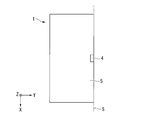
- FIG. 3A is a plan view of the LED of this embodiment.
- FIG. 3B is a side view of the LED of the present embodiment.
- FIGS. 2A to 2C an example in which the LED is manufactured by a process of cutting the LED will be described.
- the present invention is not limited to this.
- various production methods can be used as appropriate, such as production using a mold.
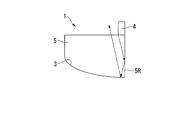
- LED1 light emitting element of this embodiment is provided with the package 2, the reflective mirror 3, the LED chip 4 (light source), and the sealing material 5, as shown in FIG.1 and FIG.3A and FIG.3B. Yes.
- a concave portion 6 having an inner wall surface in a parabolic shape is formed on the upper surface of the substantially rectangular parallelepiped package 2.
- FIG. 3A when the package 2 is viewed from above (Z direction), the outer shape of the package 2 is a rectangle.
- a metal film having high light reflectivity, a dielectric multilayer film, or the like is formed along the inner wall surface of the recess 6, and a reflection mirror 3 made of the metal film, the dielectric multilayer film, or the like is formed.
- the package 2 is made of an inorganic material or an organic material such as ceramics or metal.
- the LED chip 4 is arranged so that the light emission end face 4a faces the reflection mirror 3 as shown in FIG. 3B.
- the planar shape of the LED chip 4 is a rectangle.
- the planar shape of the LED chip 4 is not limited to a rectangle, and various shapes can be appropriately employed.
- the LED chip 4 may emit white light, or may emit monochromatic light such as red light, green light, and blue light.
- a portion of the LED 1 where the LED chip 4 on the upper surface of the sealing material 5 is not disposed is a light emission region of the LED 1.
- the recess 6 of the package 2 is filled with a sealing material 5 so that dust does not adhere to the reflection mirror 3.
- the LED chip 4 is positioned on the upper surface of the sealing material 5. It is desirable to use a material with high light transmittance for the sealing material 5, for example, epoxy resin, glass or the like.
- the sealing material 5 is filled in the recessed part 6, it is not restricted to this.
- the LED 1 is provided with wiring and the like for driving the LED chip 4.
- the wiring or the like is routed from an area other than the light emission area of the LED 1 (right side of the LED chip 4 shown in FIG. 3A).
- the configuration for driving the LED chip 4 is not limited to this, and for example, a configuration in which a wiring made of a transparent conductive film is formed on the upper surface of the sealing material 5 may be used.
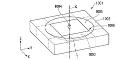
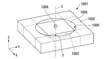
- FIG. 2A is a perspective view showing the original LED 1001 before the LED 1 of the present embodiment is cut.
- the LED 1001 before cutting includes a package 1002, a reflection mirror 1003, an LED chip 1004, and a sealing material 1005.
- the shape of the reflecting mirror 1003 is a rotationally symmetric parabolic mirror (concave mirror) centering on the central axis C shown in FIG. 2A.
- the shape of the reflection mirror 1003 is circular when viewed from above (Z direction). Circular light is emitted from the LED 1001 before cutting when viewed from above (Z direction).
- a reflection mirror 1003 having a circular shape in plan view is formed on a part (center portion) of a cubic package 1002. Therefore, a portion where light is not irradiated is generated at the end of the package 1002 outside the reflection mirror 1003.
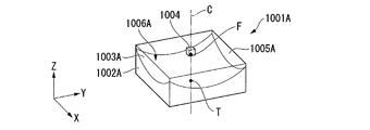
- FIG. 2B is a perspective view showing the LED 1001A obtained by cutting the LED 1001 along four sides of a square smaller than the circular reflection mirror 1003 in plan view.
- the LED 1001A cut along the four sides includes a package 1002A, a reflection mirror 1003A, an LED chip 1004, and a sealing material 1005A.
- the shape of the reflecting mirror 1003A is a rotationally symmetric parabolic mirror (concave mirror) centering on the central axis C shown in FIG. 2B.
- the shape of the reflecting mirror 1003A is a square when viewed from above (Z direction).
- FIG. 2C is a perspective view showing a shape obtained by cutting the LED 1001A along one plane S including the focal point F and the apex T of the concave mirror 1003A and passing through the midpoints of two opposite sides of the square.
- the LED 1001A is cut along the plane S to be divided into two substantially rectangular parallelepiped LEDs.
- the plane S that cuts the concave mirror 1003A includes the focal point F and the vertex T.
- the present invention is not limited to this, and includes a point slightly deviated from the focal point F and a point slightly deviated from the vertex T. You may go out. That is, the plane S only needs to include a point near the focal point and a point near the vertex. Note that the range in the vicinity may be within a range that satisfies the required directivity.
- the LED 1 of the present embodiment is one of the two substantially rectangular parallelepiped LEDs shown in FIG. 2C.
- the LED 1 of the present embodiment has a reflecting mirror 3 having a shape in which a rotationally symmetric parabolic mirror centered on a central axis C is cut in half by the plane S.
- the central axis C extending in the vertical direction of the paper surface of FIG. 3B is defined as the z axis, and is perpendicular to the z axis and is one side of the package (side extending in the horizontal direction of the paper surface of FIG. 3B).
- An axis extending parallel to the y axis is defined as a y axis, and an axis perpendicular to the z axis and the y axis is defined as an x axis.
- the LED chip 4 is arranged in such a posture that the light emission end face 4a is perpendicular to the central axis C (parallel to the xy plane).
- the LED chip 4 has a configuration in which a light emitting portion in which a light emitting layer, an electrode, and the like are laminated is formed on a semiconductor substrate.
- the LED chip 4 is disposed at the focal point F of the concave mirror 1003A.
- the present invention is not limited thereto, and the LED chip 4 may be disposed at a position slightly deviated from the focal point F. That is, it is only necessary that the LED chip is disposed in the vicinity of the focal point. Note that the range in the vicinity may be within a range that satisfies the required directivity.
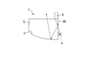
- FIG. 4A and 4B are schematic diagrams for explaining the operation of the LED 1 of the present embodiment.
- FIG. 4A is a diagram illustrating a case where light from the LED chip 4 reaches the upper part of the cut surface (reflection surface).
- FIG. 4B is a diagram illustrating a case where light from the LED chip 4 reaches the lower part of the cut surface.
- the cut surface of the LED 1 of the present embodiment is a reflecting surface 5R that reflects the light emitted from the LED chip 4, as shown in FIGS. 4A and 4B.
- a metal film having a high light reflectance is formed on the cut surface of the LED 1 of the present embodiment. Therefore, the light from the LED chip 4 is reflected by the reflecting surface 5R even if it reaches any position on the cut surface. Therefore, the light traveling from the LED chip 4 toward the cut portion does not leak to the outside, and there is no light loss.
- the present invention is not limited thereto.
- the upper part of the cutting part may be a reflecting surface so as to reflect light reaching from the LED chip 4 to the upper part of the cutting surface. That is, it is only necessary that a portion where light emitted from the LED chip 4 leaks outside without satisfying the total reflection condition at the interface with the air on the cut surface is a reflection surface.
- FIGS. 4A to 5B illustration of the package is omitted for convenience.
- the LED 2001 of the comparative example has a configuration in which the cut surface of the LED 2001 is not a reflective surface (a configuration in which the cut surface of the LED faces an external air layer). Reaching light is refracted and leaks outside. As a result, light loss occurs. That is, when the incident angle of light reaching the cut surface from the LED chip 2004 is smaller than the critical angle, the light passes through the interface. As shown in FIG. 5B, light reaching the lower part of the cut surface from the LED chip 2004 is totally reflected at the interface with air, so that no light loss occurs. That is, when the incident angle of light reaching the cut surface from the LED chip 2004 is larger than the critical angle, the light is totally reflected at the interface.
- the reflection type LED of Patent Document 1 since a part of the light emitted from the light emitting element and reflected by the reflection surface hits the lead structure (opaque wiring), the light is emitted in the region where the lead structure is arranged. The part which was not irradiated had arisen. Further, when the reflection type LED is used as a light source of the surface light source device (for example, when the reflection type LED is arranged on the end face of the light guide), it is guided at least by the size of the reflection surface of the reflection type LED. The thickness of the light body is required. Therefore, the thickness of the light guide cannot be sufficiently reduced in the surface light source device.
- the opaque wiring is not provided in the light emission area as in Patent Document 1. Therefore, the light reflected by the reflection mirror 3 is not blocked by the wiring. Therefore, LED1 which can suppress that a non-irradiation part arises can be provided.
- LED1 of this embodiment is used as a light source of a surface light source device (for example, when LED1 is arrange
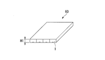
- FIG. 7A to 7B are schematic diagrams for explaining the operation of the surface light source device 60 including the LED 1 of the present embodiment.
- FIG. 7A is a perspective view for explaining the operation of the surface light source device 60 of the present embodiment.
- FIG. 7B is a perspective view for explaining the operation of the surface light source device 1060 of the comparative example.
- a plurality of cut LEDs 1 are arranged on the end face of the light guide of the surface light source device 60 of the present embodiment.
- the cut LED 1 corresponds to the LED 1 shown in FIG. Therefore, the thickness H1 of the light guide can be made substantially equal to the length of the cut LED 1 in the short direction.
- a plurality of uncut LEDs 1061 are arranged on the end face of the light guide of the surface light source device 1060 of the comparative example.
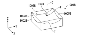
- the uncut LED 1061 corresponds to the LED 1001B shown in FIG. 6B. Therefore, the thickness H2 of the light guide is approximately equal to the length of one side of the non-cut LED 1061.
- the thickness of the light guide is reduced compared to a configuration in which non-cut LEDs are arranged. be able to. Therefore, the surface light source device 60 as a whole can be thinned.
- the surface light source device 60 that can obtain light having high directivity and can be thinned.
- the high directivity equivalent to LED which has a LED chip and a parabolic mirror of a rotational symmetry type centering on a central axis can be maintained.
- the LED 1 of the present embodiment light from the LED chip 4 is emitted toward the reflection mirror 3. That is, the light from the LED chip 4 does not directly enter the light guide, but is once reflected by the reflection mirror 3 and enters the light guide. Therefore, light with high directivity can be obtained as compared with a configuration in which light from the LED chip is directly incident on the light guide.
- the reflection mirror 3 is formed by forming a metal film or the like having a high light reflectance along the inner wall surface of the recess 6, but the metal film is formed up to the end of the cut surface. It does not have to be. In other words, the end of the reflection mirror 3 and the end of the cut surface do not necessarily coincide with each other.
- FIG. 8 is a diagram showing a simulation result of the LED 1 of the present embodiment.
- the direction of the central axis C of the LED 1 normal direction of the light emitting surface
- the directions parallel to the light emitting surface with respect to the normal direction were +90 degrees and ⁇ 90 degrees. 8 corresponds to the x-axis (direction perpendicular to the light propagation direction) in the plan view of FIG.
- the y-axis in FIG. 8 corresponds to the y-axis (perpendicular to the light propagation direction in the plan view of FIG. 3A).
- Direction the length of the rectangular parallelepiped LED 1 in the longitudinal (X) direction is 4 mm, the length in the short side (Y) direction is 2 mm, and the thickness in the Z direction (between the upper surface of the sealing material 5 and the lower surface of the package 2).
- the distance between the focal point F and the apex T was 1.5 mm.
- the length of the rectangular parallelepiped LED chip 4 in the longitudinal (X) direction was 0.32 mm
- the length in the short (Y) direction was 0.16 mm
- the thickness in the Z direction was 0.32 mm.
- the light emitted from the LED 1 has high directivity within a full width at half maximum of 16 degrees in both the x-axis direction and the y-axis direction. From this, it is estimated that the emitted light from the LED 1 has high directivity in all azimuth angles, not limited to the x-axis direction and the y-axis direction.
- FIG. 9 is a diagram showing a simulation result of the LED 2001 of the comparative example.
- LED1001A The shape of the planar view of the reflective mirror 1003A is a square LED shown in FIG. 2B is used.
- the angle of the emitted light is 0 degree in the central axis C direction (normal direction of the light emitting surface) of the LED 1001A, and +90 degrees and -90 degrees in directions parallel to the light emitting surface with respect to the normal direction. It was. 9 corresponds to the x-axis (direction perpendicular to the light propagation direction) in the perspective view of FIG. 2B, and the y-axis of FIG.
- the length of the LED 1001A in the X direction is 4 mm
- the length in the Y direction is 4 mm
- the thickness in the Z direction is 2 mm
- the focal point F and the vertex T was 1.5 mm.
- the length of one side of the cubic LED chip 1004 was set to 0.32 mm.
- the light emitted from the LED 1001A has high directivity within a full width at half maximum of 16 degrees in both the x-axis direction and the y-axis direction.
- the LED 1 having the reflection mirror 3 having the shape in which the rotationally symmetric parabolic mirror centered on the central axis C as shown in the present embodiment is cut by the plane S is used. It was confirmed that a high directivity equivalent to that of the LED 1001A having the reflection mirror 1003A having a shape before being cut by the plane S as shown can be obtained.
- disconnecting the reflective mirror 3 by the plane S demonstrated that it was a parabolic mirror
- the shape of the concave mirror that can be used in the present embodiment can be called a conical curved surface as a concept including a paraboloid.
- a curve indicating the shape of a cross section passing through the apex of a conical curved surface is called a quadratic curve, and is a curve obtained from a cross section obtained by cutting a cone on an arbitrary plane.
- the quadratic curve can be expressed by the following formulas (1) and (2).
- An example of the shape of the quadratic curve is shown in FIG. In FIG. 10, a broken line indicates a hyperbola, a thick solid line indicates a parabola, a one-dot chain line indicates an elliptic curve (short axis), a thin solid line indicates a circle, and a two-dot chain line indicates an ellipse (major axis). .
- curvature is the same in a plurality of quadratic curves.
- a concave mirror having a cross-sectional shape of these quadratic curves can be used as the concave mirror before the reflecting mirror 3 is cut along the plane S.
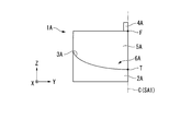
- FIG. 11 is a perspective view showing an LED 1A according to the second embodiment of the present invention.
- 12A and 12B are schematic views of the LED 1A of the present embodiment.
- FIG. 12A is a plan view of the LED 1A of the present embodiment.
- FIG. 12B is a side view of the LED 1A of the present embodiment.
- the basic configuration of the LED 1A of this embodiment is the same as that of the first embodiment, and the number of cut surfaces is different from that of the first embodiment. Therefore, the description of the basic configuration of the LED 1A is omitted in this embodiment.
- the LED 1A of the present embodiment includes a package 2A, a reflection mirror 3A, an LED chip 4A, and a sealing material 5A, as shown in FIGS. 11, 12A, and 12B.
- a recess 6A having an inner wall surface in a parabolic shape is formed.
- the outer shape of the package 2A is a square.
- the reflecting mirror 3 has a shape in which a rotationally symmetric parabolic mirror centered on the central axis C is cut by a single plane S including the focal point F and the apex T of the parabolic mirror.
- the reflecting mirror 3A is a rotationally symmetric parabolic mirror centered on the central axis C, and the focal point F and the vertex T of the parabolic mirror.
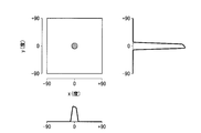
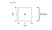
- FIG. 13 is a diagram showing a simulation result of the LED 1A of the present embodiment.
- the central axis C direction of the LED 1A normal direction of the light emitting surface
- the directions parallel to the light emitting surface with respect to the normal direction were +90 degrees and -90 degrees. 13 corresponds to the x-axis (direction perpendicular to the light propagation direction) in the plan view of FIG.
- the y-axis of FIG. 13 corresponds to the y-axis (perpendicular to the light propagation direction in the plan view of FIG. 12A).
- Direction the length of one side of the cubic LED 1A was 2 mm, and the distance between the focal point F and the vertex T was 1.5 mm.
- the LED chip 4A has a length in the X direction of 0.16 mm, a length in the Y direction of 0.16 mm, and a thickness in the Z direction of 0.32 mm.
- the light emitted from the LED 1A has high directivity within a full width at half maximum of 16 degrees in both the x-axis direction and the y-axis direction. From this, it is estimated that the emitted light from LED1A has high directivity not only in the x-axis direction and the y-axis direction but in all azimuth angles.
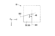
- FIG. 14 is a plan view showing LED 1B of the third embodiment of the present invention corresponding to FIG. 12A.
- the basic configuration of the LED 1B of the present embodiment is the same as that of the second embodiment, and the angles of the two planes that cut the rotationally symmetric parabolic mirror about the central axis C are different from those of the second embodiment. Therefore, the description of the basic configuration of the LED 1B is omitted in this embodiment.
- the reflecting mirror 3A has a shape in which a rotationally symmetric parabolic mirror centered on the central axis C is cut by two planes SA1 and SA2 orthogonal to each other.
- the reflecting mirror 3B is cut by two planes SB1 and SB2 where rotationally symmetric parabolic mirrors around the central axis C intersect with each other, as shown in FIG. It has a different shape.
- the angle ⁇ formed by the first plane SB1 and the second plane SB2 is an angle of less than 90 degrees.
- the angle ⁇ formed by the first plane SB1 and the second plane SB2 that are cut surfaces of the reflection mirror 3B is less than 90 degrees.
- the angle ⁇ formed by the first plane SB1 and the second plane SB2 may be greater than 90 degrees. That is, it is only necessary that the angle ⁇ formed by the first plane SB1 and the second plane SB2 is an angle other than at least 90 degrees.
- FIG. 15 is a perspective view showing an LED 1C according to the fourth embodiment of the present invention.
- 16A to 16C are diagrams showing a method for manufacturing the LED 1C of the present embodiment.
- the basic configuration of the LED 1C of this embodiment is the same as that of the second embodiment, and the shape of the reflection mirror 3C in plan view is different from that of the second embodiment. Therefore, the description of the basic configuration of the LED 1C is omitted in this embodiment.
- FIG. 16A is a perspective view showing the original LED 3001 before the LED 1C of the present embodiment is cut.
- the LED 3001 before cutting includes a package 3002, a reflection mirror 3003, an LED chip 3004, and a sealing material 3005.
- the shape of the reflection mirror 3003 is a rotationally symmetric parabolic mirror (concave mirror) centered on the central axis C shown in FIG. 16A.
- the shape of the reflection mirror 3003 is circular when viewed from above (Z direction). Circular light as seen from above (Z direction) is emitted from the LED 3001 before cutting.
- a reflection mirror 3003 having a circular shape in plan view is formed on a part (center portion) of a cubic package 3002. Therefore, a portion where light is not irradiated is generated at the end portion of the package 3002 outside the reflection mirror 3003.
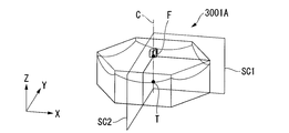
- FIG. 16B is a perspective view showing the LED 3001A obtained by cutting the LED 3001 along six sides of a regular hexagon smaller than the circular reflection mirror 3003 in plan view.
- the LED 3001A cut along the six sides includes a package 3002A, a reflection mirror 3003A, an LED chip 3004, and a sealing material 3005A.
- the shape of the reflection mirror 3003A is a rotationally symmetric parabolic mirror (concave mirror) centering on the central axis C shown in FIG. 16B.
- the shape of the reflection mirror 3003A is a regular hexagon when viewed from above (Z direction).
- FIG. 16C shows an LED 3001A including a plane SC1 including the focal point F and the vertex T of the concave mirror 3003A and passing through the regular hexagonal vertex, and a plane SC2 orthogonal to the plane SC1 (including the focal point F and the vertex T of the concave mirror 3003A).
- FIG. 6 is a perspective view showing a shape cut by a plane that passes through the midpoint of one side of a regular hexagon. As shown in FIG. 16C, the LED 3001A is cut at the planes SC1 and SC2 to obtain the LED 1C shown in FIG.
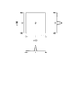
- the LED 1C includes a package 2C, a reflection mirror 3C, an LED chip 4C, and a sealing material 5C.
- a recess 6C having an inner wall surface formed in a parabolic shape is formed.
- the shape of the reflection mirror 3A in plan view is a square.
- the reflecting mirror 3C includes a rotationally symmetric planar hexagonal parabolic mirror centered on the central axis C and includes the focal point F and the apex T of the parabolic mirror. It has a shape cut by a first plane SC1 and a second plane SC2 orthogonal to the first plane.
- the LED 1C capable of obtaining light with high directivity can be realized.
- the LED 1C is defined as a surface light source, and the upper surface of the sealing material 5C is a light emission surface.
- FIG. 17 is a diagram showing a simulation result of the LED 1C of the present embodiment.
- the direction of the central axis C of the LED 1C (the normal direction of the light emitting surface) was 0 degree, and the directions parallel to the light emitting surface with respect to the normal direction were +90 degrees and ⁇ 90 degrees. 17 corresponds to the x axis (perpendicular to the light propagation direction) in the perspective view of FIG. 15, and the y axis of FIG. 17 corresponds to the y axis (perpendicular to the light propagation direction of FIG. 15).
- Direction the direction of the central axis C of the LED 1C (the normal direction of the light emitting surface) was 0 degree, and the directions parallel to the light emitting surface with respect to the normal direction were +90 degrees and ⁇ 90 degrees. 17 corresponds to the x axis (perpendicular to the light propagation direction) in the perspective view of FIG. 15, and the y axis of FIG. 17 corresponds to the y axi
- the thickness of the LED 1C was 1.7 mm, and the distance between the focal point F and the vertex T was 1.5 mm.
- the LED chip 4C has a length in the X direction of 0.16 mm, a length in the Y direction of 0.16 mm, and a thickness in the Z direction of 0.32 mm.
- the light emitted from the LED 1 ⁇ / b> C has high directivity within a full width at half maximum of 6 degrees in both the x-axis direction and the y-axis direction. From this, it is estimated that the emitted light from LED1C has high directivity not only in the x-axis direction and the y-axis direction but in all azimuth angles.
- FIG. 18 is a diagram showing a simulation result of the LED 3001A of the comparative example.
- LED3001A of a comparative example LED3001A shown in FIG. 16B (LED of which the shape of the reflection 1003A in plan view is a regular hexagon) is used.
- the angle of the emitted light is 0 degree in the central axis C direction (normal direction of the light emitting surface) of the LED 3001A, and +90 degrees and -90 degrees in directions parallel to the light emitting surface with respect to the normal direction. It was.
- the x axis in FIG. 18 corresponds to the x axis (direction perpendicular to the light propagation direction) in the perspective view of FIG.
- the length of one side of the hexagonal LED 3001A is 2.8 mm
- the thickness in the Z direction is 1.7 mm
- the distance from T was 1.5 mm.
- the length of one side of the cubic LED chip 3004 was set to 0.32 mm.
- the light emitted from the LED 3001A has a high directivity within a full width at half maximum of 6 degrees in both the x-axis direction and the y-axis direction.
- the first rotationally symmetric planar hexagonal parabolic mirror centering on the central axis C as shown in the present embodiment includes the focal point F and the apex T of the parabolic mirror.
- the shape of the reflection mirror 3003A as shown in the comparative example is a regular hexagon. It was confirmed that high directivity equivalent to that of a certain LED 3001A can be obtained.
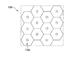
- FIG. 19A and 19B are diagrams showing a surface light source device 10A1 according to a fifth embodiment of the present invention.
- FIG. 19A is a perspective view of the surface light source device 10A1.
- FIG. 19B is a plan view of the surface light source device 10A1.
- the surface light source device 10A of this embodiment includes a plurality of LEDs 11Aa and a transparent plate 17.
- the transparent plate 17 is a plate made of a resin having optical transparency such as acrylic resin. As shown in FIG. 19A, of the six surfaces of the transparent plate 17, two main surfaces 17a and 17b facing each other are parallel. A plurality of LEDs 11 ⁇ / b> Aa are arranged on one main surface (planar region) 17 b of the transparent plate 17. In the present embodiment, the one surface 17b of the transparent plate is described as the planar region, but the present invention is not limited to this. For example, a configuration in which a transparent plate is not provided (a configuration in which a plurality of LEDs 11Aa are arranged in a predetermined plane region) may be used.
- the main surface 17b of the transparent plate 17 has a rectangular shape when viewed from the normal direction of the main surface 17b.
- an LED 11Aa having a reflection mirror having a regular hexagonal shape in a plan view of a parabolic mirror is arranged in close contact so that the sides of the regular hexagon are in contact with each other.
- 12 LEDs 11Aa are arranged.
- the surface light source device 10A1 capable of making the luminance distribution uniform.
- the planar view shape of the reflecting mirror is a regular hexagon
- the present invention is not limited thereto.
- the shape of the reflection mirror in plan view may be a triangle, a quadrangle, a pentagon, or a polygon that is a heptagon or more.
- FIG. 20 is a plan view showing a surface light source device 1010 of a comparative example corresponding to FIG. 19B.
- the gap portion is a portion that is not irradiated with light, as shown in FIG. Therefore, the luminance distribution cannot be made uniform.
- FIG. 21A and 21B are views showing a first modification of the surface light source device of the fifth embodiment of the present invention
- FIG. 21A is a perspective view showing a first modification of the surface light source device of the fifth embodiment
- FIG. 21B is a plan view showing a first modification of the surface light source device of the fifth embodiment.
- the basic configuration of the surface light source device 110A of the present modification is the same as that of the fifth embodiment, and is different from the fifth embodiment in that a transparent plate is not provided. Therefore, the description of the basic configuration of the surface light source device 110A is omitted in this modification.
- the surface light source device 110A of the present modification includes a plurality of LEDs 11Aa as shown in FIGS. 21A and 21B.
- the plurality of LEDs 11Aa are arranged in a predetermined plane area 110SA.
- the surface light source device 110A capable of achieving uniform luminance distribution. Furthermore, since a transparent plate is not required, the number of parts can be reduced and a simple configuration can be achieved.
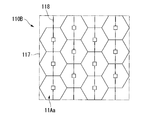
- the basic configuration of the surface light source device 110B of this modification is the same as that of the fifth embodiment, and is different from the fifth embodiment in that transparent wiring is formed on the transparent plate 117. Therefore, the description of the basic configuration of the surface light source device 110B is omitted in this modification.
- the surface light source device 110B of this modification includes a plurality of LEDs 11Aa and a transparent plate 117 as shown in FIGS. 22A and 22B.
- a wiring 118 made of a transparent conductive film is formed on one main surface (planar region) 117 b of the transparent plate 117. That is, the surface light source device 110B of the present modification has a configuration in which the wiring 118 for driving the LED chip constituting the LED 11Aa is routed on the transparent substrate 117.
- the surface light source device 110B capable of making the luminance distribution uniform. Furthermore, since the wiring 118 for driving the LED chip is formed on the transparent plate 117, the wiring can be arranged in an orderly manner.
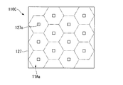
- the basic configuration of the surface light source device 110C of the present modification is the same as that of the fifth embodiment, and is different from the fifth embodiment in that a housing portion for housing the LED chip is formed on the transparent plate 117. Therefore, the description of the basic configuration of the surface light source device 110C is omitted in this modification.
- the surface light source device 110C of this modification includes a plurality of LEDs 11Aa and a transparent plate 127 as shown in FIGS. 23A and 23B.
- an accommodating portion 127c for accommodating the LED chip is formed on the side of one main surface (planar region) 127b of the transparent plate 127.
- the accommodating portion 127 c is a recess formed in the transparent plate 127. That is, in the surface light source device 110 ⁇ / b> C of this modification, the LED chip is positioned in the recess 127 c formed in the transparent substrate 127.
- the surface light source device 110C capable of making the luminance distribution uniform. Further, since the recess 127c is formed in the transparent substrate 127, the LED chip can be easily positioned.
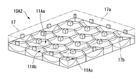
- FIG. 24A and 24B are views showing a surface light source device 10A2 according to a sixth embodiment of the present invention.
- FIG. 24A is a perspective view showing the surface light source device 10A2.
- FIG. 24B is a plan view showing the surface light source device 10A2.
- the basic configuration of the surface light source device 10A2 of this embodiment is the same as that of the fifth embodiment, and is different from the fifth embodiment in that LEDs are also arranged in the gaps of the transparent plate 17. Therefore, the description of the basic configuration of the surface light source device 10A2 is omitted in the present embodiment.
- the surface light source device 10A2 of the present embodiment includes a plurality of LEDs 11Aa, 11Ab, 11Ac, and a transparent plate 17.
- the main surface 17b of the transparent plate 17 includes a non-cutting LED 11Aa having a non-cutting mirror having a regular hexagonal shape in a plan view of a parabolic mirror, and the non-cutting mirror includes a focal point and a vertex of the noncutting mirror
- a first LED 11Ab having a shape cut by two planes and a second LED 11Ac having a shape by which the non-cutting mirror is cut by two planes orthogonal to each other are spread.
- the first LED 11Ab is an LED having a reflection mirror having the same shape as that of a non-cutting mirror whose original shape is a regular hexagon before being cut in one plane.
- the second LED 11Ac is an LED having a cutting mirror (reflection mirror) having the same shape as that of a non-cutting mirror whose original shape is a regular hexagon before being cut by two planes.
- the uncut LED 11Aa corresponds to the LED 11Aa shown in FIG. 19
- the second LED 11Ac corresponds to the LED 1C of the fourth embodiment shown in FIG.
- the non-cut LED 11Aa is disposed in close contact with the adjacent non-cut LED 11Aa.
- the first LED 11Ab and the second LED 11Ac are disposed in close contact with the non-cut LED 11Aa at a portion of the main surface 17b of the transparent plate 17 where the non-cut LED 11Aa is not disposed (end portion of the main surface 17b of the transparent plate 17).
- a total of 24 LEDs are arranged, with 12 uncut LEDs 11Aa, 10 first LEDs 11Ab, and 2 second LEDs 11Ac.
- the surface light source device 10A2 that can achieve uniform luminance distribution. Furthermore, since no gap is formed on the main surface 17b of the transparent plate 17, the LED arrangement density can be increased. As a result, the light extraction efficiency can be increased.
- a plurality of regular hexagonal non-cutting packages are prepared in advance by, for example, die molding, and cut by at least one plane as necessary.
- a cutting mirror according to this embodiment can be manufactured by forming a reflective film on the package cut in this way by vapor deposition or the like. That is, it is not necessary to prepare a cutting mirror mold separately from the non-cutting mirror mold, and the cutting mirror can be manufactured by cutting at least one plane. Therefore, the surface light source device 10 can be easily manufactured.
- planar view shape of the non-cutting mirror is a regular hexagon
- the present invention is not limited thereto.
- the planar shape of the non-cutting mirror may be a triangle, a quadrangle, a pentagon, or a polygon that is a heptagon or more.
- FIG. 25 is a plan view showing a surface light source device 10B1 according to a seventh embodiment of the present invention.
- illustration of a transparent plate is abbreviate
- the basic configuration of the surface light source device 10B1 of this embodiment is the same as that of the fifth embodiment, and only the shape of the reflection mirror in plan view is different from that of the fifth embodiment. Therefore, in this embodiment, the description of the basic configuration of the surface light source device 10B1 is omitted.
- the surface light source device 10B1 of the present embodiment includes a plurality of LEDs 11Ba and a transparent plate 17.
- the shape of the non-cutting mirror in plan view is a regular hexagon.
- the shape of the non-cutting mirror in plan view is circular.
- the main surface 17b of the transparent plate 17 is laid with LEDs 11Ba having a reflection mirror whose shape of a parabolic mirror in a plan view is circular. Specifically, the LED 11Ba is disposed on the main surface 17b of the transparent plate 17 in contact with the adjacent LED 11Ba. In the present embodiment, 18 LEDs 11Ba are arranged.
- the luminance distribution uniform it is possible to make the luminance distribution uniform.
- the surface light source device 10B1 capable of obtaining light with high directivity can be realized.
- planar view shape of a reflective mirror was circular
- planar view shape of the reflection mirror may be an ellipse
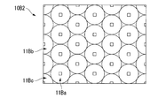
- FIG. 26 is a plan view showing a surface light source device 10B2 according to an eighth embodiment of the present invention.
- the transparent plate is not shown for convenience.
- the basic configuration of the surface light source device 10B2 of the present embodiment is the same as that of the seventh embodiment, and is different from the seventh embodiment in that LEDs are also arranged in the gap portions of the transparent plate 17. Therefore, in this embodiment, the description of the basic configuration of the surface light source device 10B2 is omitted.
- the surface light source device 10B2 of this embodiment includes a plurality of LEDs 11Ba, 11Bb, 11Bc, and a transparent plate 17.
- the main surface 17b of the transparent plate 17 includes a non-cutting LED 11Ba having a non-cutting mirror whose shape of a parabolic mirror in a plan view is circular, and the non-cutting mirror includes a focal point and a vertex of the non-cutting mirror.
- a first LED 11Bb having a shape cut by a plane and a second LED 11Bc having a shape by which the non-cutting mirror is cut by two planes orthogonal to each other are spread.
- the first LED 11Bb is an LED having a reflection mirror having the same shape as that of a non-cutting mirror whose original shape is cut in one plane.
- the second LED 11Bc is an LED having a reflection mirror having the same shape as that of a circular non-cutting mirror whose original shape before being cut by two planes.
- the non-cut LED 11Ba is arranged on the main surface 17b of the transparent plate 17 in contact with the adjacent non-cut LED 11Ba.
- the non-cutting LEDs 11Ba are arranged in a state shifted by a half pitch from the non-cutting LEDs 11Ba in the adjacent row.
- the first LED 11Bb and the second LED 11Bc are disposed in contact with the non-cut LED 11Ba at a portion of the main surface 17b of the transparent plate 17 where the non-cut LED 11Ba is not disposed (end portion of the main surface 17b of the transparent plate 17).
- a total of 32 LEDs are arranged, with 18 non-cut LEDs 11Ba, 10 first LEDs 11Bb, and 4 second LEDs 11Bc.
- the luminance distribution uniform it is possible to make the luminance distribution uniform.
- the surface light source device 10B2 capable of obtaining light with high directivity can be realized.
- the gap at the end of the main surface 17b of the transparent plate 17 can be reduced, the LED arrangement density can be increased. As a result, the light extraction efficiency can be increased.
- the shape of the non-cutting mirror and the original shape of the cutting mirror are the same, a plurality of regular hexagonal non-cutting mirrors are prepared in advance, for example, by die molding, and cut by at least one plane as necessary.
- the cutting mirror according to this embodiment can be manufactured. That is, it is not necessary to prepare a cutting mirror mold separately from the non-cutting mirror mold, and the cutting mirror can be manufactured by cutting at least one plane. Therefore, the surface light source device 10A can be easily manufactured.
- the example in which the original shape of the LED disposed in the gap at the end of the main surface 17b of the transparent plate 17 is the same circular shape as the circular non-cutting mirror is described.
- the original shape of the LEDs arranged in the gap at the end of the main surface 17b of the transparent plate 17 may be a polygon such as a regular hexagon, or may be an ellipse.
- planar view shape of the non-cutting mirror is circular
- present invention is not limited thereto.
- planar view shape of the non-cutting mirror may be elliptical.
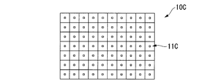
- FIGS. 27A to 27C are plan views for explaining the operation of the surface light source device 10C according to the ninth embodiment of the present invention.
- FIG. 27A is a plan view showing a surface light source device 10C of the ninth embodiment.
- FIG. 27B is a plan view showing a surface light source device 10D according to a first modification of the ninth embodiment.
- FIG. 27C is a plan view showing a surface light source device 2010 of a comparative example.
- the transparent plate is not shown for convenience.
- the basic configuration of the surface light source device 10C of this embodiment is the same as that of the fifth embodiment, and only the shape of the reflection mirror in plan view is different from that of the fifth embodiment. Therefore, in the present embodiment, the description of the basic configuration of the surface light source device 10C is omitted.
- the surface light source device 10C of this embodiment includes a plurality of LEDs 11C and a transparent plate 17.
- LEDs 11C having a square shape in a plan view of a parabolic mirror are laid.
- the LED 11C corresponds to the LED 1001A illustrated in FIG.
- the non-irradiation part is eliminated by adjusting the size of the LED 11C having a square shape in plan view with respect to the size of the main surface of the transparent plate 17.
- the LED 11C is disposed in close contact with the adjacent LEDC. In the present embodiment, a total of 35 LEDs 11C are arranged.
- the surface light source device 10C that can achieve uniform luminance distribution. Furthermore, since no gap is formed on the main surface 17b of the transparent plate 17, the LED arrangement density can be increased. As a result, the light extraction efficiency can be increased.
- the surface light source device 10D of the first modified example of the present embodiment includes a plurality of LEDs 11Da and 11Db, and a transparent plate 17.
- the main surface 17b of the transparent plate 17 includes a non-cutting LED 11Da having a non-cutting mirror having a square shape in a plan view of a parabolic mirror, and the non-cutting mirror includes a focal point and a vertex of the non-cutting mirror.
- Cut LEDs 11Db having a shape cut by a plane are laid.
- the cut LED 11Db is an LED having a reflective mirror whose shape is the same as that of a non-cut mirror whose square is cut in one plane.
- the uncut LED 11Da corresponds to the LED 1001A shown in FIG. 2B
- the cut LED 11Db corresponds to the LED 1 of the first embodiment shown in FIG.
- the non-cut LED 11Da is disposed in close contact with the adjacent non-cut LED 11Da on the main surface 17b of the transparent plate 17.
- the cut LED 11Db is disposed in close contact with the non-cut LED 11Da at the portion of the main surface 17b of the transparent plate 17 where the non-cut LED 11Da is not disposed (the lower end of the main surface 17b of the transparent plate 17).
- a total of 20 LEDs are arranged, with 15 non-cutting LEDs 11Da and 5 cutting LEDs 11Db.
- the surface light source device 10D that can achieve uniform luminance distribution. Furthermore, since no gap is formed on the main surface 17b of the transparent plate 17, the LED arrangement density can be increased. As a result, the light extraction efficiency can be increased.
- the shape of the non-cutting mirror and the original shape of the cutting mirror are the same, a plurality of square non-cutting packages are prepared in advance by, for example, die molding, and cut by at least one plane as necessary.
- the cutting mirror according to this embodiment can be manufactured. That is, it is not necessary to prepare a cutting mirror mold separately from the non-cutting mirror mold, and the cutting mirror can be manufactured by cutting at least one plane. Therefore, the surface light source device 10D can be easily manufactured.
- a configuration is considered in which LEDs 2011 having a reflecting mirror with a parabolic mirror in plan view having a square shape are arranged with a gap.
- an LED 2011 having a reflection mirror with a parabolic mirror in a plan view is arranged in contact with the upper end portion of the main surface 17 b of the transparent plate 17. Although there is a region where the LED 2011 is not disposed at the lower end portion of the main surface 17b of the transparent plate 17, a gap is generated. Thus, when the LED 2011 of the surface light source device 2010 of the comparative example is arranged with a gap, the gap portion is a portion that is not irradiated with light. Therefore, the luminance distribution cannot be made uniform.
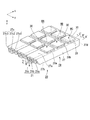
- FIG. 28 is a perspective view showing the surface light source device 20 of the present embodiment.
- FIGS. 29A to 29C are diagrams for explaining the principle in which light is emitted from each of the light extraction regions RA, RB, RC in the surface light source device 20 of the present embodiment.
- FIG. 29A shows a case where light is emitted from the first light extraction area RA.
- FIG. 29B shows a case where light is emitted from the second light extraction region RB.
- FIG. 29C shows a case where light is emitted from the third light extraction region RC.
- each of the plurality of light extraction regions has a dimming function, and the surface light source device 20 as a whole emits light only in a specific light extraction region or does not emit light. Can be.
- the amount of light emitted from a specific light extraction region can be changed with respect to the amount of light emitted from another light extraction region.
- the surface light source device 20 of the present embodiment is composed of three backlight units 24 all having the same dimensions, shape and configuration as shown in FIG.
- the three backlight units 24 are arranged adjacent to each other in a direction (y-axis direction) orthogonal to the direction in which the three light extraction regions RA, RB, RC of the light guide 27 are arranged.
- the surface light source device 20 has a total of nine light extraction regions RA, RB, RC.
- Each backlight unit 24 includes an illumination unit 21 and a light guide 27.
- the illumination unit 21 includes a plurality (three in the present embodiment) of LEDs 21a, 21b, and 21c (light sources) according to the above-described embodiment.
- the light guide 27 is composed of a parallel plate made of a resin having light permeability such as acrylic resin.
- the surface light source device 20 shows the example comprised from the three backlight units 24 by which the light guide was made into the different body here, a total of nine light extraction area
- the light guide body may have an integral structure. Even with this structure, it is possible to select the light extraction areas RA, RB, RC from which light is emitted by using the highly directional LEDs 21a, 21b, 21c according to the above-described embodiments.
- Three LEDs 21 a, 21 b, and 21 c are installed on one end face of the light guide 27 with the light emission side facing the light guide 27.
- the light guide 27 receives the light emitted from the LEDs 21a, 21b, and 21c, totally reflects the light internally, and at the opposite end surface ( ⁇ x) from the end surface side where the LEDs 21a, 21b, and 21c are installed. It has a function of propagating from the direction toward the + x direction) and taking out to the external space in the meantime. Further, the three LEDs 21a, 21b, and 21c can be individually turned on and off, and can control the amount of emitted light. Although not shown in FIG.
- the surface light source device 20 includes a printed wiring board on which the LEDs 21a, 21b, and 21c are mounted, a control unit that includes a driving IC for driving and controlling the LEDs 21a, 21b, and 21c, and the like. Is provided.
- a plurality (three in this embodiment) of light extraction regions RA, RB, and RC are arranged along the longitudinal direction (x-axis direction) of the light guide 27 on the main surface 27a of the two main surfaces of the light guide 27. Is provided.
- low refractive index bodies 28a and 28b having a refractive index lower than the refractive index of the light guide 27 and a refractive index body having a refractive index equal to the refractive index of the light guide 27 are provided.
- 29 and the low-refractive-index bodies 28a and 28b and the light-scattering body 30 that scatters the light emitted from the refractive-index body 29 are stacked in this order.
- the respective light extraction areas are directed from the side closer to the LEDs 21a, 21b, and 21c toward the side farther from the first light extraction area RA, the second light extraction area RB, and the third light extraction area RC.
- the main surface of the light guide 27 provided with the light extraction regions RA, RB, RC is the first main surface 27a
- the main surface opposite to the first main surface 27a is the second main surface 27b
- the end face of the light guide 27 provided with 21c is referred to as a first end face 27c
- the end face opposite to the first end face 27c is referred to as a second end face 27d.
- the low refractive index bodies 28 a and 28 b both have a refractive index lower than that of the light guide 27.
- the refractive index body 29 has a refractive index equal to the refractive index of the light guide body 27.
- the low refractive index bodies 28a and 28b and the refractive index body 29 have different refractive indexes.
- the low refractive index bodies 28a and 28b and the refractive index body 29 are arranged along the propagation direction of light emitted from the LEDs 21a, 21b and 21c and incident on the light extraction regions RA, RB and RC ( ⁇ x direction). From the relatively low refractive index to the relatively high refractive index.
- the refractive index nWG of the light guide 27 is 1.5, whereas the refractive index nA of the first low refractive index body 28a provided in the first light extraction region RA is 1.3.
- the refractive index nB of the second low refractive index body 28b provided in the second light extraction region RB is 1.4, and the refractive index nC of the refractive index body 29 provided in the third light extraction region RC is 1.5. Is set.
- a light scatterer 30 is stacked on the low refractive index bodies 28 a and 28 b and the refractive index body 29.
- the light scatterer 30 has a function of scattering the light incident from the low refractive index bodies 28 a and 28 b and the refractive index body 29 and extracting it to the external space of the surface light source device 20.
- a commercially available light scattering film in which scattering beads or the like are coated on the base film can be used, and the light is scattered on the low refractive index bodies 28 a and 28 b and the refractive index body 29.
- the light scatterer 30 can be formed by sticking a scattering film.
- the first end surface 27c of the light guide 27 is divided into three in the short direction (y-axis direction) of the light guide 27, and the first main surface 27a
- Three inclined surfaces 27c1, 27c2, and 27c3 having different angles are formed.
- a light guide body in which the angle between the first main surface 27a and the end surface is a right angle is prepared, and the end surface is divided into three regions. It can be formed by a method such as grinding at an angle so as to form a different angle with respect to one principal surface 27a.
- LED21a, 21b, 21c is being fixed to the approximate center of each inclined surface 27c1, 27c2, 27c3 one by one with an optical adhesive agent. Therefore, in the entire first end face 27 c, the three LEDs 21 a, 21 b, 21 c are arranged in the short direction of the light guide 27.
- the inclined surface (right side in FIG. 28) having the smallest angle with respect to the first main surface 27a is defined as the first incident end surface 27c1.
- the inclined surface (center in FIG. 28) having the next smallest angle with respect to the first main surface 27a is the second incident end surface 27c2, and the inclined surface (left side in FIG. 28) having the largest angle with respect to the first main surface 27a is the third incident end surface. 27c3.
- the LED provided on the first incident end face 27c1 is referred to as a first LED 21a
- the LED provided on the second incident end face 27c2 is referred to as a second LED 21b
- the LED provided on the third incident end face 27c3 is referred to as a third LED 21c.
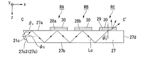
- FIG. 29A shows a cross-sectional view along the line AA ′ of FIG.
- FIG. 29B shows a cross-sectional view along the line BB ′ of FIG.
- FIG. 29C shows a sectional view taken along the line CC ′ of FIG.
- the angle beta A between the first entrance end face 27c1 and the first main surface 27a is set to 55 °.
- the angle ⁇ B formed by the second incident end face 27c2 and the first main surface 27a is set to 65 °.
- the angle ⁇ C formed between the third incident end face 27c3 and the first main surface 27a is set to 75 °.
- Each LED 21a, 21b, 21c is fixed so that light La, Lb, Lc is incident perpendicularly to each incident end face 27c1, 27c2, 27c3, and light La, Lb emitted from each LED 21a, 21b, 21c. , Lc are propagated from the first end surface 27c side to the second end surface 27d side while repeating total reflection between the first main surface 27a and the second main surface 27b of the light guide 27.
- the propagation angle ⁇ A of the light La from the first LED 21a is 35 ° as shown in FIG. 29A. It becomes.
- the propagation angle phi B light Lb from the 2LED21b becomes 25 °.
- propagation angle phi C of the light Lc from the first 3LED21c becomes 15 °. Therefore, while each light La, Lb, Lc is propagated from the first end face 27c side to the second end face 27d side, the first light extraction area RA, the second light extraction area RB, and the third light extraction area RC. In this order, the light enters the light extraction areas RA, RB, RC.
- the illumination unit 21 of the present embodiment includes three LEDs 21a, 21b, and 21c.
- the illuminating unit 21 receives light La, Lb, Lc from each LED 21a, 21b, 21c at an incident angle including an incident angle at which the light La, Lb, Lc can be extracted from each light extraction area RA, RB, RC.
- the light enters the extraction areas RA, RB, RC.
- the light La, Lb, Lc from each LED 21a, 21b, 21c is the interface between the light guide 27, the low refractive index bodies 28a, 28b, and the refractive index body 29 in each light extraction area RA, RB, RC.
- the critical angle when incident on is the critical angle when incident on.
- the two low refractive index bodies 28a, 28b and the refractive index body 29 provided in the three light extraction areas RA, RB, RC of the present embodiment are incident on the light extraction areas RA, RB, RC.
- the light is arranged in the order of relatively low refractive index to relatively high refractive index.
- the three light extraction regions RA, RB, and RC have different incident angle ranges in which light can be extracted to the outside.
- the three light extraction areas RA, RB, and RC have a relatively narrow incident angle range that can be extracted from a light extraction area that has a relatively narrow incident angle range along the propagation direction of incident light.
- incident angle range that can be extracted in the first light extraction region RA is less than 60.1 °
- incident angle range that can be extracted in the second light extraction region RB is less than 69.0 °
- third light The range of incident angles that can be extracted in the extraction region RC is arranged in the order of all angle ranges).
- the angle beta A between the first entrance end face 27c1 and the first main surface 27a is 55 °.
- the incident angle theta A with respect to the first main surface 27a of the light La from the 1LED21a becomes 55 °.
- the light guide 27 according to the present embodiment is formed of a parallel plate, the incident angle ⁇ A with respect to the first main surface 27a is always 55 ° no matter how many times the light La from the first LED 21a repeats total reflection. It is.
- the criticality here Since the angle ⁇ A is 60.1 °, the light La passes through the interface between the light guide 27 and the first low-refractive-index body 28a and is incident on the first low-refractive-index body 28a. It is scattered at 30 and taken out to the outside. In this way, substantially the entire amount of light La emitted from the first LED 21a can be extracted from the first light extraction area RA.
- the angle ⁇ B formed by the second incident end face 27c2 and the first main surface 27a is turned on. Is 65 °.
- Light Lb from the 2LED21b in order to perpendicularly incident on the second incident end face 27c2, the incident angle theta B with respect to the first main surface 27a of the light Lb from the 2LED21b becomes 65 °.
- the criticality here Since the angle ⁇ A is 60.1 °, the light Lb cannot be transmitted through the interface between the light guide 27 and the first low refractive index body 8a, and is totally reflected.
- the light La emitted from the first LED 21a is incident on the second light extraction region RB, the light La is emitted from the second light extraction region RB in order to satisfy the condition that the incident angle is smaller than the critical angle. It can be taken out. However, since almost the entire amount of the light La emitted from the first LED 21a is extracted in the first light extraction area RA before reaching the second light extraction area RB, it can almost reach the second light extraction area RB. Absent. Therefore, actually, the light La emitted from the first LED 21a is not extracted from the second light extraction region RB, and the light Lb emitted from the second LED 21b is extracted from the second light extraction region RB.
- the surface light source device 20 of the present embodiment can extract light emitted from a predetermined LED from only a predetermined light extraction region based on such a principle.
- the light Lc from the second LED 21c reaches the first light extraction area RA or the second light extraction area RB, and the interface between the light guide 27 and the first low refractive index body 28a or the second low refractive index body 28b.
- the incident angle ⁇ C 75 °
- the incident angle ⁇ C is larger than the critical angle ⁇ A and the critical angle ⁇ B , so that the light Lc cannot be transmitted through each interface and is totally reflected.
- the light Lc from the third LED 21c reaches the third light extraction region RC
- the light Lc passes through the interface between the light guide 27 and the refractive index body 29 and is incident on the refractive index body 29, and then light scattering. It is taken out from the body 30 to the outside. In this way, substantially the entire amount of the light Lc emitted from the third LED 21c can be extracted from the third light extraction region RC.
- the three light extraction areas RA depending on which of the three LEDs 21a, 21b, 21c of each backlight unit 24 is lit. It is possible to select as appropriate from which light extraction region of RB and RC light is extracted, that is, which light extraction region RA, RB, and RC emit light. Further, by controlling the amount of light emitted from each LED 21a, 21b, 21c, the amount of light extracted from the selected light extraction area RA, RB, RC, that is, the brightness of the selected light extraction area is controlled. Can be adjusted.
- the LEDs 21 a, 21 b, and 21 c according to the above-described embodiments are employed in the illumination unit 21, light with high directivity can be guided through the light guide body 27. Further, as shown in FIGS. 30A and 30B, the thickness of the light guide 27 can be reduced, and the surface light source device 20 as a whole can be reduced in thickness.
- FIGS. 30A and 30B are schematic diagrams for explaining the operation of the surface light source device 20 of the present embodiment.
- FIG. 30A is a perspective view for explaining the operation of the surface light source device 20 of the present embodiment.
- FIG. 30B is a perspective view for explaining the operation of the surface light source device 1020 of the comparative example.
- a plurality of cut LEDs 21 are arranged on the end face of the light guide of the surface light source device 20 of the present embodiment.
- the cut LED 21 corresponds to the LED 11Bb shown in FIG. Therefore, the thickness H1 of the light guide can be made substantially equal to the radius (length in the short direction) of the cut LED 21.
- a plurality of uncut LEDs 1021 are arranged on the end face of the light guide of the surface light source device 1020 of the comparative example.
- the uncut LED 1021 corresponds to the LED 11Ba shown in FIG. Therefore, the thickness H2 of the light guide is approximately equal to the diameter of the uncut LED.
- the thickness of the light guide is reduced compared to the configuration in which the non-cut LEDs are arranged. be able to. Therefore, the surface light source device 20 as a whole can be reduced in thickness.
- the first end surface 27c of the light guide 27 is different from the first to third incident end surfaces 27c1, 27c2, 27c3, which have different inclination angles with respect to the first main surface 27a.
- the configuration in which the LEDs 21a, 21b, and 21c are fixed to the incident end faces 27c1, 27c2, and 27c3 has been described as an example, but is not limited thereto.
- any shape can be adopted as long as it can guide light having high directivity through the light guide 27.
- the first end surface 27c of the light guide 27 in each backlight unit 24 is a surface perpendicular to the first main surface 27a, and the first end surface 27c has a short direction (y-axis direction) of the light guide 27.
- the three LEDs 27c1, 27c2, and 27c3 may be fixed so as to line up along the line.
- the second end face 27d of the light guide 27 is divided into three in the short direction of the light guide 27, and three inclined faces having different angles with respect to the first main face 27a are formed.
- FIG. 31 is a perspective view showing the surface light source device 40 of the present embodiment.
- 32A and 32B are cross-sectional views of the surface light source device 40 of the present embodiment.
- the surface light source device 40 of the present embodiment includes a plurality of LEDs 41 a and 41 b (light sources) according to the above-described embodiments, a light guide 47, and a plurality of reflecting units 50.
- Each reflection unit 50 includes a mirror lens 51, a light transmission unit 54, and a low refractive index unit 55.
- the light guide 47 has a function of allowing light emitted from the LEDs 41a and 41b to enter and propagating the inside while totally reflecting between the first main surface 47a and the second main surface 47b.
- the reflection unit 50 reflects a part of the light emitted from the second main surface 47b out of the light propagating through the light guide 47, changes the traveling direction of the light, and re-enters the light guide 47. And has a function of injecting from the first main surface 47a.
- 14 reflecting portions 50 are shown on the light guide 47 in the drawing, but actually, a larger number of reflecting portions 50 are provided.
- the light guide 47 is a plate made of a resin having optical transparency such as acrylic resin. As shown in FIG. 31, of the six surfaces of the light guide 47, the two main surfaces 47a and 47b facing each other are parallel to each other. Of the two end faces 47c and 47d facing each other, one end face 47c of the light guide 47 is cut obliquely with respect to the two main faces 47a and 47b.
- the first end surface 47c of the light guide 47 is divided into six in the short direction (y-axis direction) of the light guide, and two kinds of inclined surfaces having different tip angles ⁇ 1A and ⁇ 1B formed by the second main surface 47b. 47c1 and 47c2.
- the inclined surfaces 47c1 and 47c2 are alternately arranged along the short direction (y-axis direction) of the light guide 47.
- a light guide body in which the angle between the second main surface and the first end surface is a right angle is prepared, and the first end surface is divided into six regions divided into six regions.
- the two principal surfaces can be formed by a method such as grinding obliquely so as to form different angles.
- the LEDs 41 a and 41 b are arranged so that the light exit surface faces the end surface 47 c of the light guide 47.
- the LEDs 41a and 41b of the present embodiment have high directivity because they employ the LEDs according to the above-described embodiments. Therefore, the LEDs 41a and 41b emit light having a luminance distribution peak in a direction substantially perpendicular to its own light exit surface.
- Each LED 41a, 41b is fixed to the approximate center of each inclined surface 47c1, 47c2 via an optical adhesive. Therefore, six LEDs 41 a and 41 b are arranged in the short direction of the light guide 47 on the entire first end face 47 c. Moreover, lighting / extinction can be individually controlled for each of the LEDs 41a and 41b installed on the different inclined surfaces 47c1 and 47c2. With the above configuration, the surface light source device 40 of the present embodiment can propagate light at two different propagation angles inside the light guide 47.
- a plurality of reflecting portions 50 are provided on one main surface 47 b.
- the planar shape of the reflecting portion 50 viewed from the normal direction of the main surface 47b is a circle.
- the plurality of reflecting portions 50 are two-dimensionally arranged in two directions (x-axis direction and y-axis direction) orthogonal to each other in the plane of the main surface 47b. If the distance between the centers of the adjacent reflecting portions 50 is 1 pitch, the plurality of reflecting portions 50 in adjacent rows are arranged at positions shifted by 1 ⁇ 2 pitch in the row direction. Further, as shown in FIG.
- the other main surface 47a of the light guide 47 is a light emitting surface on which the light L reflected by the plurality of reflecting portions 50 is emitted.
- the main surface 47a on the side where the reflecting portion 50 is not provided is referred to as a first main surface
- the main surface 47b on the side where the reflecting portion 50 is provided is referred to as a second main surface.
- the light propagation direction in the first main surface 47a of the light guide 47 is the x-axis direction
- the direction orthogonal to the light propagation direction is the y-axis direction
- the first main surface 47a is orthogonal.
- the direction (thickness direction of the light guide 47) is defined as the z-axis direction. Therefore, the “light propagation direction” in the present embodiment refers to the direction in which light (indicated by the dashed line arrow L) propagates while reflecting in the xz section of the light guide 47 shown in FIGS. 32A and 32B. It does not mean, but means a direction (indicated by a solid arrow X) in which light propagates when viewed from the normal direction of the first main surface 47a of the light guide 47.
- each reflecting portion 50 includes a mirror lens 51 including a convex lens 52 and a concave mirror 53, a light transmitting portion 54, and a low refractive index portion 55.
- the convex lens 52 is made of a resin having optical transparency such as acrylic resin.
- the convex lens 52 is a so-called plano-convex lens in which one surface 52a is a flat surface (light emitting surface) and the other surface 52b is a parabolic surface (reflecting surface).
- the concave mirror 53 is composed of a metal thin film with high reflectivity, such as aluminum, formed along the parabolic surface 52 b of the convex lens 52.
- the shape of the top part into which the light L injects is a paraboloid shape
- the shape of a side part is a cylindrical shape.
- the concave mirror 53 may have at least a parabolic shape in which the light L is incident through the light transmitting portion 54, but the entire concave mirror 53 may have a parabolic shape.
- the concave mirror 53 has a paraboloid at least in part, it has a focal point P.
- the light transmission part 54 is a columnar member made of a resin having light permeability such as acrylic resin.
- the light transmissive resin constituting the light transmissive portion 54 the same type as the light transmissive resin constituting the light guide 47 is used. For this reason, the light transmission portion 54 has a refractive index equal to the refractive index of the light guide 47.
- the light transmissive resin constituting the light transmissive portion 54 may be of a different type from the light transmissive resin constituting the light guide 47.
- the light transmitting portion 54 may have a refractive index higher than that of the light guide 47.
- the light transmissive resin constituting the light transmissive portion 54 may be the same type as the light transmissive resin constituting the convex lens 52 or may be a different type.
- the light transmission part 54 may have a refractive index equal to the refractive index of the convex lens 52 or may have a refractive index higher than that of the convex lens 52.
- the light transmission part 54 has a function of connecting the light guide 47 and the mirror lens 51 and guiding the light L propagating through the light guide 47 to the mirror lens 51.
- the mirror lens 51 is fixed to the light guide 47 in a posture in which the flat surface 52 a side of the convex lens 52 is opposed to the second main surface 47 b of the light guide 47.
- the diameter of the light transmission part 54 is sufficiently smaller than the diameter of the mirror lens 51.
- the light transmission part 54 is provided only at the focal point P of the concave mirror 53 and its vicinity, as shown in FIGS.
- the focal point P of the concave mirror 53 is preferably located at the interface between the light transmission part 54 and the mirror lens 51, but may be located inside the light transmission part 54, or may be guided to the light transmission part 54. It may be located at the interface with the light body 47.
- a low-refractive-index part 55 is provided in a part of the region sandwiched between the flat surface 5 a of the convex lens 52 and the second main surface 47 b of the light guide 47 and surrounding the light transmission part 54.
- the low refractive index portion 55 is made of a positive type ultraviolet curable resin.
- the ultraviolet curable resin constituting the low refractive index portion 55 has a refractive index lower than that of the light guide 47.
- the refractive index of each part when the refractive index of the light guide 47 is 1.5, the refractive index of the light transmission part 54 is 1.5, the refractive index of the low refractive index part 55 is 1.3, The refractive index of the convex lens 52 is 1.5.
- the constituent material of each part can mention an acrylic resin as a constituent material of the light guide 47, for example.
- the material of the light transmitting portion 54 and the convex lens 52 include a liquid material of methacrylic resin “Parapet (optical grade)” (registered trademark, refractive index: 1.49) manufactured by Kuraray Co., Ltd.
- the material of the low refractive index portion 55 include a liquid material of amorphous fluororesin “AF1600” (registered trademark, refractive index: 1.3) manufactured by DuPont.
- an inclined surface having a large tip angle with the second main surface 47b (for example, the second inclined surface from the right in FIG. 31).
- An inclined surface having a small tip angle formed by the first incident end surface 47c1 and the second main surface 47b (for example, the rightmost inclined surface in FIG. 31) is referred to as a second incident end surface 47c2.
- the LED provided on the first incident end face 47c1 is referred to as a first LED 41a
- the LED provided on the second incident end face 47c2 is referred to as a second LED 41b.
- FIG. 32A shows a cross-sectional view taken along the line D-D ′ of FIG.
- FIG. 32B shows a cross-sectional view along the line E-E ′ of FIG. 31.
- the tip angle ⁇ 1A formed by the first incident end face 47c1 and the second main surface 47b is set to 65 °
- a tip angle ⁇ 1B formed by the end surface 47c2 and the second main surface 47b is set to 55 °.
- Each LED 41a, 41b is fixed so that light La, Lb is incident perpendicularly to each incident end face 47c1, 47c2.
- each LED 41a, 41b repeats total reflection between the first main surface 47a and the second main surface 47b of the light guide 47 and is second from the first end surface 47c side. Propagated toward the end face 47d side.
- the first LED 41a is turned on and the second LED 41b is turned off.
- the incident angle ⁇ 1A of the light La with respect to the second main surface 47b of the light guide 47 is 65 °.
- the first main surface 47a of the light guide 47 is an interface between a substance having a refractive index of 1.5 and air having a refractive index of 1.0.
- the critical angle of the first major surface 47a of the light guide 47 is about 42 °. That is, light having an incident angle ⁇ 1 of 42 ° or more with respect to the first main surface 47a of the light guide 47 is totally reflected on the first main surface 47a of the light guide 47. The same applies to the second main surface 47b of the light guide 47.
- the region where the low refractive index portion 55 exists is an interface between a substance having a refractive index of 1.5 and a substance having a refractive index of 1.3.
- the critical angle at the interface between the second major surface 47b of the light guide 47 and the low refractive index portion 55 is about 60.1 °. That is, light having an incident angle ⁇ of 60.1 ° or more with respect to the interface between the second main surface 47b of the light guide 47 and the low refractive index portion 55 is totally reflected on the second main surface 47b of the light guide 47.
- the critical angle at the interface between the second main surface 47b of the light guide 47 and the low refractive index portion 55 is about 60.1 °
- the second main surface 3b of the light guide 47 and the low refractive index portion 55 Light having an incident angle ⁇ with respect to the interface of 60.1 ° or more is totally reflected at the second main surface 3 b of the light guide 47. Therefore, when the light La emitted from the first LED 41 a reaches the interface between the second main surface 47 b of the light guide 47 and the low refractive index portion 55, the light La is totally reflected at the interface and is incident on the low refractive index portion 55. There is nothing.
- the critical angle at the interface between the second main surface 47 b of the light guide 47 and the low refractive index portion 55 is about 60.1 °
- the light Lb emitted from the second LED 41 b is the second main surface of the light guide 47.
- the light Lb passes through a position greatly deviated from the focal point P of the concave mirror 53, the light Lb travels in various directions that are not perpendicular to the second main surface 47b of the light guide 47 after being reflected by the concave mirror 53. .
- the second LED 41b is selectively turned on, light having high directivity cannot be obtained, and light having a wide angle range can be obtained.
- a mode in which light having high directivity is obtained and a mode in which light having a wide angle range is obtained depending on which of the first LED 41a and the second LED 41b is turned on. Can be switched.
- this surface light source device 40 is used as a backlight of a liquid crystal display device, a mode in which highly directional light can be obtained from the viewpoint of energy saving, privacy protection, and the like may be used when viewing the display by one person.
- a mode in which light having a wide angle range can be obtained so that anyone can easily see the display may be used.
- the first LED 41a and the second LED 41b according to the above-described embodiments are employed, light having high directivity can be guided through the light guide 47. Moreover, the thickness of the light guide 47 can be reduced, and the surface light source device 40 as a whole can be reduced in thickness.
- FIG. 33A and 33B are diagrams showing the simulation results.
- the angle of the emitted light is the front direction when viewed from the first main surface of the light guide, that is, the normal direction of the first main surface is 0 degree, and the direction parallel to the first main surface with respect to the normal direction is +90. Degree and -90 degrees.
- 33A and 33B corresponds to the x-axis (light propagation direction) in the perspective view of FIG. 33A and 33B correspond to the y-axis (direction perpendicular to the light propagation direction) in the perspective view of FIG.
- the simulation conditions were such that the diameter of the mirror lens 51 was 100 ⁇ m, the radius of curvature of the paraboloid of the mirror lens 51 was 50 ⁇ m, and the diameter of the cylindrical body of the light transmitting portion 54 was 5 ⁇ m.
- FIG. 34 is a cross-sectional view of the liquid crystal display device 100 of the present embodiment.
- the liquid crystal display device 100 (display device) of this embodiment includes a backlight 102 (surface light source device), a first polarizing plate 103, a liquid crystal panel 104, and a second polarizing plate according to the above-described embodiment.
- the liquid crystal display body 106 (display body) which has 105, and the viewing angle expansion film 107 are comprised.
- the liquid crystal panel 104 is schematically illustrated as a single plate.
- the observer views the display from the upper side of the liquid crystal display device 100 in FIG. 34 in which the viewing angle widening film 107 is arranged. Therefore, in the following description, the side on which the viewing angle widening film 107 is disposed is referred to as a viewing side, and the side on which the backlight 102 is disposed is referred to as a back side.
- the light emitted from the backlight 102 is modulated by the liquid crystal panel 104, and a predetermined image, character, or the like is displayed by the modulated light. Further, when the light emitted from the liquid crystal panel 104 passes through the viewing angle widening film 107, the angle distribution of the emitted light becomes wider than before entering the viewing angle widening film 107, and the light is widened. Is injected from. Thereby, the observer can visually recognize the display with a wide viewing angle.
- an active matrix transmissive liquid crystal panel is described as an example, but a liquid crystal panel applicable to the present embodiment is not limited to an active matrix transmissive liquid crystal panel.
- the liquid crystal panel applicable to the present embodiment may be, for example, a transflective (transmission / reflection type) liquid crystal panel or a reflection type liquid crystal panel, and each pixel has a switching thin film transistor (Thin Film Transistor, hereinafter). Or a simple matrix type liquid crystal panel that is not provided with TFT).
- the backlight 102 includes the LED 136 according to the above-described embodiment, and a light guide plate 137 that emits light toward the liquid crystal panel 104 using internal reflection of light emitted from the LED 136.
- the backlight 102 may be an edge light type in which LEDs are disposed on the end face of the light guide, or may be a direct type in which a light source is disposed directly under the light guide.
- a so-called directional backlight which has a directivity by controlling the light emission direction, is used.
- the base 139 is arranged on the viewing side, so that the surface with the smaller area of the two opposing surfaces of the truncated cone-shaped light diffusion portion 140 is The light exit end face, and the surface with the larger area becomes the light incident end face.
- the inclination angle of the side surface of the light diffusing unit 140 (angle formed between the light emitting end surface and the side surface) is about 80 ° as an example.
- the inclination angle of the side surface of the light diffusing unit 140 is not particularly limited as long as it is an angle that can sufficiently diffuse incident light when exiting from the viewing angle widening film 107.
- the backlight 102 since the backlight 102 according to the above-described embodiment is employed, collimated or substantially collimated light can be incident on the light diffusion portion of the viewing angle widening film 107. The light is diffused in all directions by the viewing angle widening film 107. Therefore, a good image with little color change can be obtained when viewed from any direction.
- the thickness of the backlight 102 can be reduced, and the entire liquid crystal display device 100 can be reduced in thickness.
- the display device 200 of the present embodiment includes a backlight 242 (surface light source device), a liquid crystal element 243 (light modulation element), and a light emitting element 244 similar to that of the above embodiment. It is equipped with.
- a red sub-pixel 245R that performs display using red light
- a green sub-pixel 245G that performs display using green light
- a blue sub-pixel 245B that performs display using blue light are disposed adjacent to each other.
- These three subpixels 245R, 45G, and 45B constitute one pixel that is a minimum unit that constitutes a display.
- the backlight 242 emits excitation light L1 that excites the phosphor layers 246R, 46G, and 46B of the light emitting element 244, and emits ultraviolet light or blue light as the excitation light L1 in this embodiment.
- the liquid crystal element 243 modulates the transmittance of the excitation light L1 emitted from the backlight 242 for each of the subpixels 245R, 245G, and 245B.
- the light emitting element 244 receives the excitation light L1 modulated by the liquid crystal element 243, and the phosphor layers 246R, 246G, and 246B are excited and emitted light is emitted to the outside. Therefore, in the present embodiment, the upper side of the display device 200 shown in FIG. 35 is the viewing side where the user views the display.
- the liquid crystal element 243 has a configuration in which a liquid crystal layer 249 is sandwiched between a first transparent substrate 247 and a second transparent substrate 248.
- the second transparent substrate 248 located on the front side as viewed from the user also serves as the substrate of the light emitting element in the above embodiment.
- a first polarizing plate 251 is provided on the outer surface of the first transparent substrate 247 (the surface opposite to the liquid crystal layer side).
- the first transparent substrate 247 a substrate that can transmit excitation light, such as glass, quartz, or plastic, can be used.
- a transparent conductive material such as indium tin oxide (hereinafter abbreviated as ITO) is used.
- ITO indium tin oxide
- the first polarizing plate 251 a conventional general external polarizing plate can be used.
- a phosphor layer 246 and a first light absorption layer 259 are laminated in this order from the substrate side on the inner surface (surface on the liquid crystal layer 249 side) of the second transparent substrate 248.
- the phosphor material constituting the phosphor layer 246 has a different emission wavelength band for each subpixel.
- the red subpixel 245R is provided with a phosphor layer 246R made of a phosphor material that absorbs ultraviolet light and emits red light, and the green subpixel 245G.
- a phosphor layer 246G made of a phosphor material that absorbs ultraviolet light and emits green light
- the blue subpixel 245B has a fluorescence made of a phosphor material that absorbs ultraviolet light and emits blue light.
- a body layer 246B is provided.
- the red subpixel 245R and the green subpixel 245G are made of phosphor materials that absorb ultraviolet light and emit red light and green light, respectively.
- the blue subpixel 245B is provided with a light diffusion layer that diffuses the blue light, which is excitation light, without converting the wavelength and emits the light to the outside instead of the phosphor layer.
- a second polarizing plate 253 is formed on the inner surface of the second transparent substrate 248 so as to cover the first light absorption layer 259, and a second transparent electrode 254 and an alignment film (not shown) are formed on the surface of the second polarizing plate 253. ) Are stacked.
- the second polarizing plate 253 is a so-called in-cell polarizing plate that is formed using a coating technique or the like in the manufacturing process of the liquid crystal element 243.
- a transparent conductive material such as ITO is used for the second transparent electrode 254.
- the method of the liquid crystal element 243 is not particularly limited, and for example, an active matrix method including a switching element such as a thin film transistor (hereinafter abbreviated as TFT) for each subpixel may be employed. A passive matrix method without a TFT may be adopted.
- the mode of the liquid crystal layer 249 is not particularly limited, and various liquid crystal modes such as a TN (Twisted Nematic) mode, a VA (Vertical Alignment) mode, and an IPS (In-Plane Switching) mode can be employed.
- the phosphor layers 246R, 46G, and 46B, the first light absorption layer 59, the second polarizing plate 253, and the second transparent electrode 254 are laminated in this order from the substrate side on the inner surface side of the second transparent substrate 248. Further, a second light absorption layer 260 is formed on the outer surface side of the second transparent substrate 248.
- the first light absorption layer 259 is for suppressing a decrease in contrast due to leakage of the excitation light L1 from the backlight 242.
- the 2nd light absorption layer 260 is for suppressing the contrast fall by external light.
- the first light absorption layer 259 and the second light absorption layer 260 may be made of the same phosphor material, or may be made of different phosphor materials in accordance with excitation light and external light.
- the backlight 242 since the backlight 242 according to the above-described embodiment is employed, collimated or substantially collimated light can be incident on the liquid crystal element 243.
- the excitation light modulated by the liquid crystal element 243 is color-converted by the phosphor layer 246 and isotropically emitted to the outside. Therefore, a good image with little color change can be obtained when viewed from any direction. Further, the thickness of the backlight 242 can be reduced, and the display device 200 as a whole can be reduced in thickness.
- FIGS. 36A and 36B are diagrams illustrating a configuration example of a lighting device.
- FIG. 36A is a plan view of the lighting device.
- 36B is a cross-sectional view taken along the line FF ′ of FIG. 36A.
- a character portion 301 written “SHARP” is formed on one surface of the light guide 27.
- a first low refractive index body 28a having a refractive index of 1.3 is formed on the first main surface 27a side of the light guide 27, and the character portion 301 is formed.
- the first low-refractive-index body 28a is not formed in the other portions.
- a light scatterer 30 is stacked on the first low refractive index body 28a. That is, the character portion 301 is a light extraction area in the above embodiment.
- FIG. 36B only one first end surface 27c is shown, but in reality, another one first end surface having a different angle with respect to the first main surface 27a is formed in the depth direction of the paper surface. Although only one LED 21a is shown in the drawing, actually, another LED is installed in the depth direction of the paper surface.
- this illumination device 300 light is emitted from the character portion 301 or light is emitted from other than the character portion 301 depending on which of the two LEDs provided on the first end surface 27c of the light guide 27 is turned on. Can be switched. Therefore, according to this structure, the illuminating device which can be utilized as a digital signage which can blink the character part 301, for example is realizable.
- the aspect of the present invention can be used in the fields of light-emitting elements, surface light source devices, display devices, and illumination devices.
Landscapes
- Physics & Mathematics (AREA)
- General Physics & Mathematics (AREA)
- Optics & Photonics (AREA)
- Nonlinear Science (AREA)
- Mathematical Physics (AREA)
- Chemical & Material Sciences (AREA)
- Crystallography & Structural Chemistry (AREA)
- Planar Illumination Modules (AREA)
- Liquid Crystal (AREA)
- Led Device Packages (AREA)
- Light Guides In General And Applications Therefor (AREA)
- Optical Couplings Of Light Guides (AREA)
Abstract
発光素子は、光源と、前記光源から射出された光を反射させる反射ミラーと、を含む。前記反射ミラーは、内部に凹面形状の反射面を有する凹面ミラーが前記凹面ミラーの焦点近傍の点と頂点近傍の点とを含む少なくとも1つの平面で切断された形状を有し、前記光源は前記反射ミラーの前記焦点近傍に配置され、前記光源からの光が前記反射ミラーの前記反射面に向けて射出される。
Description
本発明は、発光素子、面光源装置、表示装置および照明装置に関するものである。
本願は、2011年8月5日に、日本に出願された特願2011-171768号に基づき優先権を主張し、その内容をここに援用する。
本願は、2011年8月5日に、日本に出願された特願2011-171768号に基づき優先権を主張し、その内容をここに援用する。
指向性を有する光を射出可能な発光ダイオード(Light Emitting Diode,以下、LEDと略記する)が提案されている。例えば、特許文献1には、内部に凹面形状の反射面を有する凹状ケースと、凹状ケースの開口部側中央に素子マウント部が位置するように設けられたリード構造と、リード構造の素子マウント部に配置された発光素子と、を備えた反射型LEDが開示されている。
特許文献1に記載の反射型LEDにおいては、発光素子から射出されて反射面により反射された光の一部がリード構造に当たるため、前記リード構造が配置された領域において光が照射されない部分が生じる。
また、前記反射型LEDを面光源装置の光源として用いた場合(例えば前記反射型LEDを導光体の端面に配置した場合)においては、少なくとも反射型LEDの反射面の大きさの分だけ導光体の厚みが必要になる。そのため、面光源装置において導光体の厚みを十分に薄くすることができない。
また、前記反射型LEDを面光源装置の光源として用いた場合(例えば前記反射型LEDを導光体の端面に配置した場合)においては、少なくとも反射型LEDの反射面の大きさの分だけ導光体の厚みが必要になる。そのため、面光源装置において導光体の厚みを十分に薄くすることができない。
本発明の態様は、非照射部が生じることを抑制することが可能な発光素子を提供することを目的とする。導光体の薄型化を図ることが可能な面光源装置を提供することを目的とする。この種の面光源装置を備えた表示装置および照明装置を提供することを目的とする。
本発明の一態様における発光素子は、光源と、前記光源から射出された光を反射させる反射ミラーと、を含み、前記反射ミラーは、内部に凹面形状の反射面を有する凹面ミラーが前記凹面ミラーの焦点近傍の点と頂点近傍の点とを含む少なくとも1つの平面で切断された形状を有し、前記光源は前記反射ミラーの前記焦点近傍に配置され、前記光源からの光が前記反射ミラーの前記反射面に向けて射出される。
本発明の一態様における発光素子において、前記反射ミラーは、前記凹面ミラーが1つの前記平面で切断された形状を有してもよい。
本発明の一態様における発光素子において、前記反射ミラーは、前記凹面ミラーが互いに交差する2つの前記平面で切断された形状を有してもよい。
本発明の一態様における発光素子において、前記反射ミラーは、前記凹面ミラーが互いに直交する2つの前記平面で切断された形状を有してもよい。
本発明の一態様における発光素子において、前記反射ミラーの前記平面で切断された面の少なくとも一部が前記光源から射出された光を反射させる反射面となっていてもよい。
本発明の他の態様における面光源装置は、複数の上記発光素子と、前記複数の発光素子から射出された光が入射され、前記光を内部で伝播させて前記光を外部に取り出す導光体と、を備え、前記導光体の端面には、前記複数の発光素子が配置されている。
本発明の他の態様における面光源装置において、前記導光体は、前記複数の発光素子の少なくとも一つから射出された光を内部で全反射させて伝播させ、前記光を外部に取り出す光取出領域を有し、前記導光体の端面には、前記光取出領域が設けられた面に対する角度が互いに異なる複数の傾斜面が設けられ、前記複数の発光素子の各々が、前記複数の傾斜面の各々に固定されていてもよい。
本発明の他の態様における面光源装置において、上記発光素子を含み、前記複数の発光素子が、平面領域に複数配置されていてもよい。
本発明の他の態様における面光源装置において、前記平面領域は、前記平面領域の法線方向から見て矩形状となっており、前記平面領域には、前記平面で切断されていない前記凹面ミラーを有する非切断ミラーと、少なくとも1つの前記平面で切断された形状を有する前記反射ミラーとしての切断ミラーとが互いに接するよう配置されていてもよい。
本発明の他の態様における面光源装置において、前記非切断ミラーは、前記平面領域の法線方向から見た形状が多角形となっており、前記切断ミラーは、前記平面で切断される前のもとの形状が前記平面領域の法線方向から見て多角形の前記非切断ミラーの形状と同一の形状となっており、前記平面領域には、多角形の前記非切断ミラーが隣り合う多角形の前記非切断ミラーと密着して配置され、前記平面領域の多角形の前記非切断ミラーが配置されていない部分には、もとの形状が多角形の前記非切断ミラーの形状と同一の形状の前記切断ミラーが多角形の前記非切断ミラーと密着して配置されることにより、多角形の前記非切断ミラーと前記切断ミラーとが前記平面領域に配置されていてもよい。
本発明の他の態様における面光源装置において、前記非切断ミラーは、前記平面領域の法線方向から見た形状が円形となっていてもよい。
本発明の他の態様における面光源装置において、前記切断ミラーは前記平面で切断される前のもとの形状が前記平面領域の法線方向から見て円形の前記非切断ミラーの形状と同一の形状となっており、前記平面領域には、円形の前記非切断ミラーが隣り合う円形の前記非切断ミラーと接して配置され、前記平面領域の円形の前記非切断ミラーが配置されていない部分には、もとの形状が円形の前記非切断ミラーの形状と同一の形状の前記切断ミラーが円形の前記非切断ミラーと接して配置されることにより、円形の前記非切断ミラーと前記切断ミラーとが前記平面領域に配置されていてもよい。
本発明のさらに他の態様における面光源装置は、光源と、前記光源から射出された光を反射させる反射ミラーと、を含み、前記反射ミラーは、内部に凹面形状の反射面を有し、前記光源は前記反射ミラーの焦点近傍に配置され、前記光源からの光が前記反射ミラーの前記反射面に向けて射出される構成とされた複数の発光素子を備え、前記複数の発光素子が、平面領域に互いに接するように配置されている。
本発明のさらに他の態様における面光源装置において、前記反射ミラーは、前記平面領域の法線方向から見た形状が多角形となっており、前記平面領域には、多角形の前記反射ミラーが隣り合う多角形の前記反射ミラーと密着して配置されていてもよい。
本発明のさらに他の態様における面光源装置において、前記反射ミラーは、前記平面領域の法線方向から見た形状が円形となっており、前記平面領域には、円形の前記反射ミラーが隣り合う円形の前記反射ミラーと接して配置されていてもよい。
本発明のさらに他の態様における表示装置は、上記面光源装置と、前記面光源装置から射出される光を用いて表示を行う表示素子と、を備える。
本発明のさらに他の態様における照明装置は、上記面光源装置を備える。
本発明の態様によれば、矩形状の平面領域に複数の発光素子を配置する場合において、輝度分布の均一化を図ることが可能な発光素子、面光源装置、表示装置および照明装置を提供することができる。
以下に実施形態及び実施例を挙げ、本発明の態様を更に詳細に説明するが、本発明の態様はこれらの実施形態及び実施例に限定されるものではない。
なお、以下の全ての図面においては、各構成要素を見やすくするため、構成要素によって寸法の縮尺を異ならせて示すことがある。
なお、以下の全ての図面においては、各構成要素を見やすくするため、構成要素によって寸法の縮尺を異ならせて示すことがある。
[第1実施形態]
図1は、本発明の第1実施形態のLED(発光素子)を示す斜視図である。図2A~図2Cは、本実施形態のLEDの作製方法を示す図である。図3A~図3Bは、本実施形態のLEDの模式図であり、図3Aは本実施形態のLEDの平面図である。図3Bは、本実施形態のLEDの側面図である。なお、図2A~図2Cにおいては、LEDを切断していくとういうプロセスで作製する例を挙げて説明するが、これに限らない。例えば、金型を用いて作製するなど、適宜種々の作製方法を用いることができる。
図1は、本発明の第1実施形態のLED(発光素子)を示す斜視図である。図2A~図2Cは、本実施形態のLEDの作製方法を示す図である。図3A~図3Bは、本実施形態のLEDの模式図であり、図3Aは本実施形態のLEDの平面図である。図3Bは、本実施形態のLEDの側面図である。なお、図2A~図2Cにおいては、LEDを切断していくとういうプロセスで作製する例を挙げて説明するが、これに限らない。例えば、金型を用いて作製するなど、適宜種々の作製方法を用いることができる。
本実施形態のLED1(発光素子)は、図1および図3A及び図3Bに示すように、パッケージ2と、反射ミラー3と、LEDチップ4(光源)と、封止材5と、を備えている。略直方体状のパッケージ2の上面に、内壁面が放物面形状となった凹部6が形成されている。図3Aに示すように、パッケージ2を上方(Z方向)から見ると、パッケージ2の外形形状は長方形である。凹部6の内壁面に沿って光反射率の高い金属膜、誘電体多層膜等が形成されており、これら金属膜、誘電体多層膜等からなる反射ミラー3が形成されている。パッケージ2は、例えばセラミックス、金属等の無機材料もしくは有機材料で構成されている。
LEDチップ4は、図3Bに示すように、光射出端面4aが反射ミラー3に対向するように配置されている。本実施形態では、図3Aに示すように、LEDチップ4の平面形状は長方形である。なお、LEDチップ4の平面形状は長方形に限られず、適宜種々の形状を採用することができる。LEDチップ4は、白色光を射出するものであっても良いし、赤色光、緑色光、青色光等の単色光を射出するものであっても良い。なお、LED1において封止材5上面のLEDチップ4が配置されていない部分が、LED1の光射出領域となる。
パッケージ2の凹部6内には、反射ミラー3に塵が付着しないように封止材5が充填されている。封止材5の上面にはLEDチップ4が位置決めされている。封止材5には光透過率が高い材料を用いることが望ましく、例えばエポキシ樹脂、ガラス等が用いられる。
なお、本実施形態では、凹部6内に封止材5が充填されているが、これに限らない。例えば、凹部6内が中空であってもよい。凹部6内が中空の場合、凹部6内の屈折率と外部の空気の屈折率とが等しくなる(n=1)。そのため、LED1から射出される光の指向性を維持することができる。
その他、図示を省略するが、LED1には、LEDチップ4を駆動するための配線等が備えられている。例えば、配線等はLED1の光射出領域以外の領域(図3Aに示すLEDチップ4右側)から引き回されている。なお、LEDチップ4を駆動するための構成はこれに限らず、例えば封止材5の上面に透明導電膜からなる配線が形成された構成であってもよい。
なお、本実施形態では、凹部6内に封止材5が充填されているが、これに限らない。例えば、凹部6内が中空であってもよい。凹部6内が中空の場合、凹部6内の屈折率と外部の空気の屈折率とが等しくなる(n=1)。そのため、LED1から射出される光の指向性を維持することができる。
その他、図示を省略するが、LED1には、LEDチップ4を駆動するための配線等が備えられている。例えば、配線等はLED1の光射出領域以外の領域(図3Aに示すLEDチップ4右側)から引き回されている。なお、LEDチップ4を駆動するための構成はこれに限らず、例えば封止材5の上面に透明導電膜からなる配線が形成された構成であってもよい。
図2Aは、本実施形態のLED1が切断される前のもとのLED1001を示した斜視図である。図2Aに示すように、切断前のLED1001は、パッケージ1002と、反射ミラー1003と、LEDチップ1004と、封止材1005と、を備えている。反射ミラー1003の形状は、図2Aに示す中心軸Cを中心とした回転対称形の放物面ミラー(凹面ミラー)である。反射ミラー1003の形状は上方(Z方向)から見ると円形である。切断前のLED1001からは上方(Z方向)から見て円形の光が射出される。当該LED1001では、立方体形状のパッケージ1002の一部(中心部分)に平面視円形の反射ミラー1003が形成されている。そのため、反射ミラー1003の外側のパッケージ1002の端部において光が照射されない部分が生じる。
図2Bは、LED1001を、平面視円形の反射ミラー1003よりも小さい正方形の4辺で切断したLED1001Aを示した斜視図である。図2Bに示すように、前記4辺で切断したLED1001Aは、パッケージ1002Aと、反射ミラー1003Aと、LEDチップ1004と、封止材1005Aと、を備えている。反射ミラー1003Aの形状は、図2Bに示す中心軸Cを中心とした回転対称形の放物面ミラー(凹面ミラー)である。反射ミラー1003Aの形状は上方(Z方向)から見ると正方形である。このように、切断前のLED1001を平面視円形の反射ミラー1003よりも小さい正方形の4辺で切断することによって、パッケージ1002Aの反射ミラー1003Aと平面視重ならない部分が切り落とされる。そのため、前記4辺で切断後のLED1001Aにおいては、切断前のパッケージ1002の端部に相当する部分がない。よって、光が照射されない部分が生じない。
なお、本実施形態では、LED1001を、平面視円形の反射ミラー1003よりも小さい正方形の4辺で切断したLED1001Aを示したが、これに限らない。例えば、図6A~図6Cに示すように、LED1001を、平面視円形の反射ミラー1003に内接する正方形の4辺で切断したLED1001Bにおいても本実施形態を適用することができる。
なお、本実施形態では、LED1001を、平面視円形の反射ミラー1003よりも小さい正方形の4辺で切断したLED1001Aを示したが、これに限らない。例えば、図6A~図6Cに示すように、LED1001を、平面視円形の反射ミラー1003に内接する正方形の4辺で切断したLED1001Bにおいても本実施形態を適用することができる。
図2Cは、LED1001Aを、凹面ミラー1003Aの焦点Fと頂点Tとを含み正方形の対向する2辺の中点を通る1つの平面Sで切断した形状を示した斜視図である。
図2Cに示すように、LED1001Aが当該平面Sで切断されることにより、二つの略直方体状のLEDに分割される。
なお、本実施形態では凹面ミラー1003Aを切断する平面Sが焦点Fと頂点Tとを含んでいるが、これに限らず、焦点Fから少しずれた点と頂点Tから少しずれた点とを含んでいてもよい。すなわち、平面Sが焦点近傍の点と頂点近傍の点とを含んでいればよい。
なお、近傍の範囲は要求される指向性を満足させるような範囲内であればよい。
図2Cに示すように、LED1001Aが当該平面Sで切断されることにより、二つの略直方体状のLEDに分割される。
なお、本実施形態では凹面ミラー1003Aを切断する平面Sが焦点Fと頂点Tとを含んでいるが、これに限らず、焦点Fから少しずれた点と頂点Tから少しずれた点とを含んでいてもよい。すなわち、平面Sが焦点近傍の点と頂点近傍の点とを含んでいればよい。
なお、近傍の範囲は要求される指向性を満足させるような範囲内であればよい。
本実施形態のLED1は、図2Cに示す分割された二つの略直方体状のLEDのうちの一方のLEDである。本実施形態のLED1は、中心軸Cを中心とした回転対称形の放物面ミラーが前記平面Sで半分に切断された形状の反射ミラー3を有している。以下の説明では、図3Bの紙面の縦方向に延びる中心軸Cをz軸と定義し、z軸に対して垂直であって、かつパッケージの一辺(図3Bの紙面の横方向に延びる辺)に平行に延びる軸をy軸、z軸およびy軸に垂直な軸をx軸、と定義する。
LEDチップ4は、光射出端面4aが中心軸Cに垂直(xy平面に対して平行)になる姿勢で配置されている。詳細には、LEDチップ4は、発光層や電極等が積層されてなる発光部が半導体基板上に形成された構成である。
なお、本実施形態ではLEDチップ4が凹面ミラー1003Aの焦点Fに配置されているが、これに限らず、焦点Fから少しずれた位置に配置されていてもよい。すなわち、LEDチップが焦点近傍に配置されていればよい。なお、近傍の範囲は要求される指向性を満足させるような範囲内であればよい。
なお、本実施形態ではLEDチップ4が凹面ミラー1003Aの焦点Fに配置されているが、これに限らず、焦点Fから少しずれた位置に配置されていてもよい。すなわち、LEDチップが焦点近傍に配置されていればよい。なお、近傍の範囲は要求される指向性を満足させるような範囲内であればよい。
図4A及び図4Bは、本実施形態のLED1の作用を説明するための模式図である。図4Aは、LEDチップ4からの光が切断面(反射面)の上部に届いた場合を示す図である。図4Bは、LEDチップ4からの光が切断面の下部に届いた場合を示す図である。
本実施形態のLED1の切断面は、図4A及び図4Bに示すように、LEDチップ4から射出された光を反射させる反射面5Rとなっている。例えば、本実施形態のLED1の切断面には、光反射率の高い金属膜が形成されている。そのため、LEDチップ4からの光は切断面のいずれの位置に届いた場合であっても反射面5Rで反射される。よって、LEDチップ4から切断部に向かう光は外部に漏れることがなく、光の損失がない。
なお、本実施形態においては、LED1の切断面の全面を反射面5Rとした例を挙げて説明したが、これに限らない。例えば、LEDチップ4から切断面の上部に届く光を反射させるよう切断部の上部のみが反射面となっていてもよい。すなわち、LEDチップ4から射出された光が切断面における空気との界面で全反射条件を満足せずに外部に漏れてしまう部分のみが反射面となっていればよい。
ここで、比較例のLED2001として切断面が反射面となっていない構成(LEDの切断面が外部の空気層に面する構成)を考える。
図5A及び図5Bは、比較例のLED2001の作用を説明するための模式図である。図5Aは、LEDチップ2004からの光が切断面の上部に届いた場合を示す図である。図5Bは、LEDチップ2004からの光が切断面の下部に届いた場合を示す図である。なお、図4A~図5Bにおいては、便宜上パッケージの図示を省略している。
図5A及び図5Bは、比較例のLED2001の作用を説明するための模式図である。図5Aは、LEDチップ2004からの光が切断面の上部に届いた場合を示す図である。図5Bは、LEDチップ2004からの光が切断面の下部に届いた場合を示す図である。なお、図4A~図5Bにおいては、便宜上パッケージの図示を省略している。
比較例のLED2001の切断面が反射面となっていない構成(LEDの切断面が外部の空気層に面する構成)であると、図5Aに示すように、LEDチップ2004から切断面の上部に届く光は屈折して外部に漏れてしまう。そのため、光の損失が生じる。つまり、LEDチップ2004から切断面に届く光の入射角が臨界角よりも小さいときは光が界面を透過してしまう。なお、図5Bに示すように、LEDチップ2004から切断面の下部に届く光は空気との界面で全反射するため、光の損失は生じない。つまり、LEDチップ2004から切断面に届く光の入射角が臨界角よりも大きいときは光が界面で全反射する。
ところで、特許文献1の反射型LEDにおいては、発光素子から射出されて反射面により反射された光の一部がリード構造(不透明の配線)に当たるため、前記リード構造が配置された領域において光が照射されない部分が生じていた。
また、前記反射型LEDを面光源装置の光源として用いた場合(例えば前記反射型LEDを導光体の端面に配置した場合)においては、少なくとも反射型LEDの反射面の大きさの分だけ導光体の厚みが必要になる。そのため、面光源装置において導光体の厚みを十分に薄くすることができない。
また、前記反射型LEDを面光源装置の光源として用いた場合(例えば前記反射型LEDを導光体の端面に配置した場合)においては、少なくとも反射型LEDの反射面の大きさの分だけ導光体の厚みが必要になる。そのため、面光源装置において導光体の厚みを十分に薄くすることができない。
これに対して、本実施形態のLED1では、特許文献1のように光射出領域に不透明の配線が設けられていない。そのため、反射ミラー3で反射された光が配線に遮られることがない。よって、非照射部が生じることを抑制することが可能なLED1を提供することができる。
また、本実施形態のLED1を面光源装置の光源として用いた場合(例えばLED1を導光体の端面に配置した場合)においては、図7に示すように、導光体の厚みを小さくすることができ、面光源装置60全体として薄型化を図ることができる。
図7A~図7Bは、本実施形態のLED1を備えた面光源装置60の作用を説明するための模式図である。図7Aは、本実施形態の面光源装置60の作用を説明するための斜視図である。図7Bは、比較例の面光源装置1060の作用を説明するための斜視図である。
図7Aに示すように、本実施形態の面光源装置60の導光体の端面には複数の切断LED1が配置されている。なお、切断LED1は、図1に示すLED1に相当する。そのため、導光体の厚みH1を切断LED1の短手方向の長さと概ね等しくすることができる。
図7Bに示すように、比較例の面光源装置1060の導光体の端面には複数の非切断LED1061が配置されている。なお、非切断LED1061は、図6Bに示すLED1001Bに相当する。そのため、導光体の厚みH2は非切断LED1061の一辺の長さと概ね等しくなる。
このように、本実施形態においては、面光源装置60の導光体の端面に複数の切断LED1を配置することにより、非切断LEDを配置した構成に比べて、導光体の厚みを小さくすることができる。よって、面光源装置60全体として薄型化を図ることができる。
このように、本実施形態によれば指向性の高い光を得るとともに薄型化を図ることが可能な面光源装置60を実現できる。
また、本実施形態のLED1の形状であっても、LEDチップと中心軸を中心とした回転対称形の放物面ミラーとを有するLEDと同等の高い指向性を維持することができる。
また、本実施形態のLED1においては、LEDチップ4からの光が反射ミラー3に向けて射出される。すなわち、LEDチップ4からの光は、直接導光体内に入射するのではなく、一旦反射ミラー3で反射されて導光体内に入射する。そのため、LEDチップからの光が直接導光体内に入射する構成に比べて、指向性の高い光を得ることができる。
なお、本実施形態においては、凹部6の内壁面に沿って光反射率の高い金属膜等が形成されることにより反射ミラー3が形成されているが、金属膜は切断面の端部まで形成されていなくてもよい。すなわち、反射ミラー3の端部と切断面の端部が必ずしも一致している必要はない。
本実施形態のLED1の効果を実証するため、シミュレーションによりLED1から射出される光の角度-輝度プロファイルを求めた。ただし、LED1は面光源として定義しており、封止材5の上面が光射出面となっている。
図8は、本実施形態のLED1のシミュレーション結果を示す図である。射出光の角度は、LED1の中心軸C方向(光射出面の法線方向)を0度とし、法線方向を基準として光射出面に平行な方向を+90度および-90度とした。図8のx軸は図3Aの平面図におけるx軸(光の伝播方向に垂直な方向)に対応し、図8のy軸は図3Aの平面図におけるy軸(光の伝播方向に垂直な方向)に対応している。シミュレーションの条件として、直方体形状のLED1の長手(X)方向の長さを4mm、短手(Y)方向の長さを2mm、Z方向の厚み(封止材5上面とパッケージ2下面との間の距離)を2mm、焦点Fと頂点Tとの間の距離を1.5mmとした。また、直方体形状のLEDチップ4の長手(X)方向の長さを0.32mm、短手(Y)方向の長さを0.16mm、Z方向の厚みを0.32mmとした。
図8は、本実施形態のLED1のシミュレーション結果を示す図である。射出光の角度は、LED1の中心軸C方向(光射出面の法線方向)を0度とし、法線方向を基準として光射出面に平行な方向を+90度および-90度とした。図8のx軸は図3Aの平面図におけるx軸(光の伝播方向に垂直な方向)に対応し、図8のy軸は図3Aの平面図におけるy軸(光の伝播方向に垂直な方向)に対応している。シミュレーションの条件として、直方体形状のLED1の長手(X)方向の長さを4mm、短手(Y)方向の長さを2mm、Z方向の厚み(封止材5上面とパッケージ2下面との間の距離)を2mm、焦点Fと頂点Tとの間の距離を1.5mmとした。また、直方体形状のLEDチップ4の長手(X)方向の長さを0.32mm、短手(Y)方向の長さを0.16mm、Z方向の厚みを0.32mmとした。
図8に示すように、LED1からの射出光は、x軸方向、y軸方向の双方ともに、半値全幅16度以内の高い指向性を持つことが確認された。このことから、LED1からの射出光は、x軸方向、y軸方向に限らず、全ての方位角において高い指向性を持つことが推測される。
図9は、比較例のLED2001のシミュレーション結果を示す図である。なお、比較例のLEDとしては、図2Bに示すLED1001A(反射ミラー1003Aの平面視の形状が正方形のLED)を用いる。図9において、射出光の角度は、LED1001Aの中心軸C方向(光射出面の法線方向)を0度とし、法線方向を基準として光射出面に平行な方向を+90度および-90度とした。図9のx軸は図2Bの斜視図におけるx軸(光の伝播方向に垂直な方向)に対応し、図9のy軸は図2Bの斜視図におけるy軸(光の伝播方向に垂直な方向)に対応している。シミュレーションの条件として、LED1001AのX方向の長さを4mm、Y方向の長さを4mm、Z方向の厚み(封止材上面とパッケージ下面との間の距離)を2mm、焦点Fと頂点Tとの間の距離を1.5mmとした。また、立方体形状のLEDチップ1004の一辺の長さを0.32mmとした。
図9に示すように、LED1001Aからの射出光は、x軸方向、y軸方向の双方ともに、半値全幅16度以内の高い指向性を持つことが確認された。
以上のことから、本実施形態に示すような中心軸Cを中心とした回転対称形の放物面ミラーが平面Sで切断された形状の反射ミラー3を有するLED1であっても、比較例に示すような平面Sで切断する前の形状の反射ミラー1003Aを有するLED1001Aと同等な高い指向性を得ることができることが確認された。
なお、本実施形態においては、反射ミラー3を平面Sで切断する前の凹面ミラーの形状が放物面ミラーであると説明したが、これに限らない。例えば、本実施形態で用いることが可能な凹面ミラーの形状は、放物面を含む概念として円錐曲面ということができる。円錐曲面の頂点を通る断面の形状を示す曲線は二次曲線と呼ばれ、円錐を任意の平面で切り取った断面から得られる曲線である。二次曲線は下記の(1)式、(2)式で表すことができる。


(1)式、(2)式におけるコーニック係数kの値によって二次曲線は形を変える。二次曲線は、例えばk=0のときに円となり、-1<k<0のときに楕円曲線となり、k=-1のときに放物線となり、k<-1のときに双曲線となる。二次曲線の形状の例を図10に示す。図10において、破線が双曲線を示し、太い実線が放物線を示し、1点鎖線が楕円曲線(短軸)を示し、細い実線が円を示し、二点鎖線が楕円(長軸)を示している。
なお、複数の二次曲線において曲率は同じである。本実施形態では、反射ミラー3を平面Sで切断する前の凹面ミラーとして、これらの二次曲線を断面形状とする凹面ミラーを用いることもできる。
なお、複数の二次曲線において曲率は同じである。本実施形態では、反射ミラー3を平面Sで切断する前の凹面ミラーとして、これらの二次曲線を断面形状とする凹面ミラーを用いることもできる。
[第2実施形態]
図11は、本発明の第2実施形態のLED1Aを示す斜視図である。図12A及び図12Bは、本実施形態のLED1Aの模式図である。図12Aは、、本実施形態のLED1Aの平面図である。図12Bは、、本実施形態のLED1Aの側面図である。
図11は、本発明の第2実施形態のLED1Aを示す斜視図である。図12A及び図12Bは、本実施形態のLED1Aの模式図である。図12Aは、、本実施形態のLED1Aの平面図である。図12Bは、、本実施形態のLED1Aの側面図である。
本実施形態のLED1Aの基本構成は第1実施形態と同様であり、切断面の数が第1実施形態と異なる。そのため、本実施形態ではLED1Aの基本構成の説明は省略する。
本実施形態のLED1Aは、図11、図12A、及び図12Bに示すように、パッケージ2Aと、反射ミラー3Aと、LEDチップ4Aと、封止材5Aと、を備えている。パッケージ2Aの上面に、内壁面が放物面形状となった凹部6Aが形成されている。図12Aに示すように、パッケージ2Aを光射出側から見ると、パッケージ2Aの外形形状は正方形である。
第1実施形態では、反射ミラー3が、中心軸Cを中心とした回転対称形の放物面ミラーが前記放物面ミラーの焦点Fと頂点Tとを含む1つの平面Sで切断された形状を有していた。これに対して、本実施形態では、反射ミラー3Aが、図12Aに示すように、中心軸Cを中心とした回転対称形の放物面ミラーが前記放物面ミラーの焦点Fと頂点Tとを含む第1の平面SA1と前記第1の平面SA1に直交する第2の平面SA2とで切断された形状を有している。
本実施形態においても、輝度分布の均一化を図ることが可能となる。また、指向性の高い光を得ることが可能なLED1Aを実現できる。
本発明者らは、本実施形態のLED1Aの効果を実証するため、シミュレーションによりLED1Aから射出される光の角度-輝度プロファイルを求めた。ただし、LED1Aは面光源として定義しており、封止材5Aの上面が光射出面となっている。
図13は、本実施形態のLED1Aのシミュレーション結果を示す図である。射出光の角度は、LED1Aの中心軸C方向(光射出面の法線方向)を0度とし、法線方向を基準として光射出面に平行な方向を+90度および-90度とした。図13のx軸は図12Aの平面図におけるx軸(光の伝播方向に垂直な方向)に対応し、図13のy軸は図12Aの平面図におけるy軸(光の伝播方向に垂直な方向)に対応している。シミュレーションの条件として、立方体形状のLED1Aの一辺の長さを2mm、焦点Fと頂点Tとの間の距離を1.5mmとした。また、LEDチップ4AのX方向の長さを0.16mm、Y方向の長さを0.16mm、Z方向の厚みを0.32mmとした。
図13は、本実施形態のLED1Aのシミュレーション結果を示す図である。射出光の角度は、LED1Aの中心軸C方向(光射出面の法線方向)を0度とし、法線方向を基準として光射出面に平行な方向を+90度および-90度とした。図13のx軸は図12Aの平面図におけるx軸(光の伝播方向に垂直な方向)に対応し、図13のy軸は図12Aの平面図におけるy軸(光の伝播方向に垂直な方向)に対応している。シミュレーションの条件として、立方体形状のLED1Aの一辺の長さを2mm、焦点Fと頂点Tとの間の距離を1.5mmとした。また、LEDチップ4AのX方向の長さを0.16mm、Y方向の長さを0.16mm、Z方向の厚みを0.32mmとした。
図13に示すように、LED1Aからの射出光は、x軸方向、y軸方向の双方ともに、半値全幅16度以内の高い指向性を持つことが確認された。このことから、LED1Aからの射出光は、x軸方向、y軸方向に限らず、全ての方位角において高い指向性を持つことが推測される。
以上のことから、本実施形態に示すような中心軸Cを中心とした回転対称形の放物面ミラーが互いに直交する2つの平面SA1,SA2で切断された形状の反射ミラー3Aを有するLED1Aであっても、比較例に示すような平面Sで切断する前の形状の反射ミラー1003Aを有するLED1001Aと同等な高い指向性を得ることができることが確認された。
[第3実施形態]
図14は、図12Aに対応した、本発明の第3実施形態のLED1Bを示す平面図である。
図14は、図12Aに対応した、本発明の第3実施形態のLED1Bを示す平面図である。
本実施形態のLED1Bの基本構成は第2実施形態と同様であり、中心軸Cを中心とした回転対称形の放物面ミラーを切断する2つの平面の角度が第2実施形態と異なる。そのため、本実施形態ではLED1Bの基本構成の説明は省略する。
第2実施形態では、反射ミラー3Aが、中心軸Cを中心とした回転対称形の放物面ミラーが互いに直交する2つの平面SA1,SA2で切断された形状を有していた。これに対して、本実施形態では、反射ミラー3Bが、図14に示すように、中心軸Cを中心とした回転対称形の放物面ミラーが互いに交差する2つの平面SB1,SB2で切断された形状を有している。本実施形態では第1の平面SB1と第2の平面SB2とのなす角度θが90度未満の角度となっている。
本実施形態においても、輝度分布の均一化を図ることが可能となる。また、指向性の高い光を得ることが可能なLED1Bを実現できる。
なお、本実施形態においては、反射ミラー3Bの切断面となる第1の平面SB1と第2の平面SB2とのなす角度θが90度未満の角度となっている例を挙げて説明したが、これに限らない。例えば、第1の平面SB1と第2の平面SB2とのなす角度θが90度より大きくなっていてもよい。すなわち、第1の平面SB1と第2の平面SB2とのなす角度θが少なくとも90度以外の角度となっていればよい。
[第4実施形態]
図15は、本発明の第4実施形態のLED1Cを示す斜視図である。図16A~図16Cは、本実施形態のLED1Cの作製方法を示す図である。
図15は、本発明の第4実施形態のLED1Cを示す斜視図である。図16A~図16Cは、本実施形態のLED1Cの作製方法を示す図である。
本実施形態のLED1Cの基本構成は第2実施形態と同様であり、反射ミラー3Cの平面視の形状が第2実施形態と異なる。そのため、本実施形態ではLED1Cの基本構成の説明は省略する。
図16Aは、本実施形態のLED1Cが切断される前のもとのLED3001を示した斜視図である。図16Aに示すように、切断前のLED3001は、パッケージ3002と、反射ミラー3003と、LEDチップ3004と、封止材3005と、を備えている。反射ミラー3003の形状は、図16Aに示す中心軸Cを中心とした回転対称形の放物面ミラー(凹面ミラー)である。反射ミラー3003の形状は上方(Z方向)から見ると円形である。切断前のLED3001からは上方(Z方向)から見て円形の光が射出される。前記LED3001では、立方体形状のパッケージ3002の一部(中心部分)に平面視円形の反射ミラー3003が形成されている。そのため、反射ミラー3003の外側のパッケージ3002の端部において光が照射されない部分が生じる。
図16Bは、LED3001を、平面視円形の反射ミラー3003よりも小さい正六角形の6辺で切断したLED3001Aを示した斜視図である。図16Bに示すように、前記6辺で切断したLED3001Aは、パッケージ3002Aと、反射ミラー3003Aと、LEDチップ3004と、封止材3005Aと、を備えている。反射ミラー3003Aの形状は、図16Bに示す中心軸Cを中心とした回転対称形の放物面ミラー(凹面ミラー)である。反射ミラー3003Aの形状は上方(Z方向)から見ると正六角形である。このように、切断前のLED3001を平面視円形の反射ミラー1003よりも小さい正六角形の6辺で切断することによって、パッケージ3002Aの反射ミラー3003Aと平面視重ならない部分が切り落とされる。そのため、前記6辺で切断後のLED3001Aにおいては、切断前のパッケージ3002の端部に相当する部分がない。
よって、光が照射されない部分が生じない。
なお、本実施形態では、LED3001を、平面視円形の反射ミラー3003よりも小さい正六角形の6辺で切断したLED3001Aを示したが、これに限らない。例えば、LED3001を、平面視円形の反射ミラー3003に内接する正六角形の6辺で切断したLEDにおいても本発明を適用することができる。
よって、光が照射されない部分が生じない。
なお、本実施形態では、LED3001を、平面視円形の反射ミラー3003よりも小さい正六角形の6辺で切断したLED3001Aを示したが、これに限らない。例えば、LED3001を、平面視円形の反射ミラー3003に内接する正六角形の6辺で切断したLEDにおいても本発明を適用することができる。
図16Cは、LED3001Aを、凹面ミラー3003Aの焦点Fと頂点Tとを含み正六角形の頂点を通る平面SC1と、前記平面SC1に直交する平面SC2(凹面ミラー3003Aの焦点Fと頂点Tとを含み正六角形の1辺の中点を通る平面)と、で切断した形状を示した斜視図である。図16Cに示すように、LED3001Aが当該平面SC1とSC2とで切断されることにより、図15に示すLED1Cが得られる。
本実施形態のLED1Cは、図15に示すように、パッケージ2Cと、反射ミラー3Cと、LEDチップ4Cと、封止材5Cと、を備えている。パッケージ2Cの上面に、内壁面が放物面形状となった凹部6Cが形成されている。
第2実施形態では、反射ミラー3Aの平面視の形状が正方形であった。これに対して、本実施形態では、反射ミラー3Cが、中心軸Cを中心とした回転対称形の平面視正六角形の放物面ミラーが前記放物面ミラーの焦点Fと頂点Tとを含む第1の平面SC1と前記第1の平面に直交する第2の平面SC2とで切断された形状を有している。
本実施形態においても、指向性の高い光を得ることが可能なLED1Cを実現できる。
本実施形態のLED1Cの効果を実証するため、シミュレーションによりLED1Cから射出される光の角度-輝度プロファイルを求めた。ただし、LED1Cは面光源として定義しており、封止材5Cの上面が光射出面となっている。
図17は、本実施形態のLED1Cのシミュレーション結果を示す図である。射出光の角度は、LED1Cの中心軸C方向(光射出面の法線方向)を0度とし、法線方向を基準として光射出面に平行な方向を+90度および-90度とした。図17のx軸は図15の斜視図におけるx軸(光の伝播方向に垂直な方向)に対応し、図17のy軸は図15の斜視図におけるy軸(光の伝播方向に垂直な方向)に対応している。シミュレーションの条件として、LED1Cの厚みを1.7mm、焦点Fと頂点Tとの間の距離を1.5mmとした。また、LEDチップ4CのX方向の長さを0.16mm、Y方向の長さを0.16mm、Z方向の厚みを0.32mmとした。
図17に示すように、LED1Cからの射出光は、x軸方向、y軸方向の双方ともに、半値全幅6度以内の高い指向性を持つことが確認された。このことから、LED1Cからの射出光は、x軸方向、y軸方向に限らず、全ての方位角において高い指向性を持つことが推測される。
図18は、比較例のLED3001Aのシミュレーション結果を示す図である。なお、比較例のLED3001Aとしては、図16Bに示すLED3001A(反射1003Aの平面視の形状が正六角形のLED)を用いる。図18において、射出光の角度は、LED3001Aの中心軸C方向(光射出面の法線方向)を0度とし、法線方向を基準として光射出面に平行な方向を+90度および-90度とした。図18のx軸は図16Bの斜視図におけるx軸(光の伝播方向に垂直な方向)に対応し、図18のy軸は図16Bの斜視図におけるy軸(光の伝播方向に垂直な方向)に対応している。シミュレーションの条件として、六角柱形状のLED3001Aの六角形の一辺の長さを2.8mm、Z方向の厚み(封止材上面とパッケージ下面との間の距離)を1.7mm、焦点Fと頂点Tとの間の距離を1.5mmとした。また、立方体形状のLEDチップ3004の一辺の長さを0.32mmとした。
図18に示すように、LED3001Aからの射出光は、x軸方向、y軸方向の双方ともに、半値全幅6度以内の高い指向性を持つことが確認された。
以上のことから、本実施形態に示すような中心軸Cを中心とした回転対称形の平面視正六角形の放物面ミラーが前記放物面ミラーの焦点Fと頂点Tとを含む第1の平面と前記第1の平面に直交する第2の平面とで切断された形状の反射ミラー3Cを有するLED1Cであっても、比較例に示すような反射ミラー3003Aの平面視の形状が正六角形であるLED3001Aと同等な高い指向性を得ることができることが確認された。
[第5実施形態]
本実施形態では、例えば液晶表示装置のバックライトとして用いて好適な面光源装置の一例を示す。
図19A及び図19Bは、本発明の第5実施形態の面光源装置10A1を示す図である。図19Aは、面光源装置10A1の斜視図である。図19Bは、面光源装置10A1平面図である。
本実施形態では、例えば液晶表示装置のバックライトとして用いて好適な面光源装置の一例を示す。
図19A及び図19Bは、本発明の第5実施形態の面光源装置10A1を示す図である。図19Aは、面光源装置10A1の斜視図である。図19Bは、面光源装置10A1平面図である。
本実施形態の面光源装置10Aは、複数のLED11Aaと、透明板17と、を備えている。
透明板17は、例えばアクリル樹脂等の光透過性を有する樹脂からなる板体である。図19Aに示すように、透明板17の6つの面のうち、互いに対向する2つの主面17a,17bは平行である。透明板17の一つの主面(平面領域)17bには、複数のLED11Aaが配置されている。なお、本実施形態では平面領域として透明板の一面17bを挙げて説明しているが、これに限らない。例えば、透明板が設けられていない構成(所定の平面領域に複数のLED11Aaが配置された構成)であってもよい。
透明板17の主面17bは、前記主面17bの法線方向から見て矩形状になっている。
透明板17の主面17bには、放物面ミラーの平面視の形状が正六角形の反射ミラーを有するLED11Aaが正六角形の辺どうしが接するように密着して配置されている。本実施形態においては、LED11Aaが12個配置されている。
透明板17の主面17bには、放物面ミラーの平面視の形状が正六角形の反射ミラーを有するLED11Aaが正六角形の辺どうしが接するように密着して配置されている。本実施形態においては、LED11Aaが12個配置されている。
本実施形態においては輝度分布の均一化を図ることが可能な面光源装置10A1を実現できる。
なお、本実施形態においては、反射ミラーの平面視形状が正六角形である例を挙げて説明したが、これに限らない。例えば、反射ミラーの平面視形状が三角形、四角形、五角形、及び7角形以上の多角形であってもよい。
ここで、比較例の面光源装置1010として放物面ミラーの平面視の形状が正六角形の反射ミラーを有するLED1011が隙間を有して配置されている構成を考える。
図20は、図19Bに対応した、比較例の面光源装置1010を示す平面図である。
図20は、図19Bに対応した、比較例の面光源装置1010を示す平面図である。
比較例の面光源装置1010のLED1011が隙間を有して配置されている構成であると、図20に示すように、前記隙間部分は光が照射されない部分となる。そのため、輝度分布の均一化を図ることができない。
[第5実施形態の第1変形例]
図21A及び図21Bは、本発明の第5実施形態の面光源装置の第1変形例を示す図であり、図21Aは、第5実施形態の面光源装置の第1変形例を示す斜視図、図21Bは、第5実施形態の面光源装置の第1変形例を示す平面図である。
図21A及び図21Bは、本発明の第5実施形態の面光源装置の第1変形例を示す図であり、図21Aは、第5実施形態の面光源装置の第1変形例を示す斜視図、図21Bは、第5実施形態の面光源装置の第1変形例を示す平面図である。
本変形例の面光源装置110Aの基本構成は第5実施形態と同様であり、透明板が設けられていない点が第5実施形態と異なる。そのため、本変形例では面光源装置110Aの基本構成の説明は省略する。
本変形例の面光源装置110Aは、図21A及び図21Bに示すように、複数のLED11Aaを備えている。複数のLED11Aaは、所定の平面領域110SAに配置されている。
本変形例においても輝度分布の均一化を図ることが可能な面光源装置110Aを実現できる。さらに、透明板を必要としないため、部品点数を少なくし簡素な構成とすることができる。
[第5実施形態の第2変形例]
本変形例の面光源装置110Bの基本構成は第5実施形態と同様であり、透明板117に透明な配線が形成されている点が第5実施形態と異なる。そのため、本変形例では面光源装置110Bの基本構成の説明は省略する。
本変形例の面光源装置110Bは、図22A及び図22Bに示すように、複数のLED11Aaと、透明板117と、を備えている。透明板117の一つの主面(平面領域)117bには、透明導電膜からなる配線118が形成されている。すなわち、本変形例の面光源装置110Bは、透明基板117にLED11Aaを構成するLEDチップを駆動するための配線118が引き回された構成となっている。
本変形例においても輝度分布の均一化を図ることが可能な面光源装置110Bを実現できる。さらに、透明板117にLEDチップを駆動するための配線118が形成されているため、配線の引き回しを整然とすることができる。
[第5実施形態の第3変形例]
本変形例の面光源装置110Cの基本構成は第5実施形態と同様であり、透明板117にLEDチップを収容するための収容部が形成されている点が第5実施形態と異なる。そのため、本変形例では面光源装置110Cの基本構成の説明は省略する。
本変形例の面光源装置110Cは、図23A及び図23Bに示すように、複数のLED11Aaと、透明板127と、を備えている。透明板127の一つの主面(平面領域)127bの側には、LEDチップを収容するための収容部127cが形成されている。本変形例において、収容部127cは、透明板127に形成された窪みである。すなわち、本変形例の面光源装置110Cは、透明基板127に形成された窪み127cにLEDチップが位置決めされている。
本変形例においても輝度分布の均一化を図ることが可能な面光源装置110Cを実現できる。さらに、透明基板127に窪み127cが形成されているため、LEDチップの位置決めが容易となる。
[第6実施形態]
図24A及び図24Bは、本発明の第6実施形態の面光源装置10A2を示す図である。図24Aは、面光源装置10A2を示す斜視図である。図24Bは、面光源装置10A2を示す平面図である。
図24A及び図24Bは、本発明の第6実施形態の面光源装置10A2を示す図である。図24Aは、面光源装置10A2を示す斜視図である。図24Bは、面光源装置10A2を示す平面図である。
本実施形態の面光源装置10A2の基本構成は第5実施形態と同様であり、透明板17の隙間部分にもLEDが配置されている点が第5実施形態と異なる。そのため、本実施形態では面光源装置10A2の基本構成の説明は省略する。
本実施形態の面光源装置10A2は、複数のLED11Aa,11Ab,11Acと、透明板17と、を備えている。
透明板17の主面17bには、放物面ミラーの平面視の形状が正六角形の非切断ミラーを有する非切断LED11Aaと、前記非切断ミラーが前記非切断ミラーの焦点と頂点とを含む1つの平面で切断された形状を有する第1LED11Abと、前記非切断ミラーが互いに直交する2つの平面で切断された形状を有する第2LED11Acと、が敷き詰められている。第1LED11Abは、1つの平面で切断される前のもとの形状が正六角形の非切断ミラーの形状と同一の形状の反射ミラーを有するLEDである。第2LED11Acは、2つの平面で切断される前のもとの形状が正六角形の非切断ミラーの形状と同一の形状の切断ミラー(反射ミラー)を有するLEDである。なお、本実施形態において、非切断LED11Aaは、図19に示すLED11Aaに相当し、第2LED11Acは、図15に示す第4実施形態のLED1Cに相当する。
具体的には、透明板17の主面17bには、非切断LED11Aaが隣り合う非切断LED11Aaと密着して配置されている。透明板17の主面17bの非切断LED11Aaが配置されていない部分(透明板17の主面17bの端部)には、第1LED11Abおよび第2LED11Acが非切断LED11Aaと密着して配置されている。本実施形態においては、非切断LED11Aaが12、第1LED11Abが10、第2LED11Acが2つ、の計24のLEDが配置されている。
本実施形態においても輝度分布の均一化を図ることが可能な面光源装置10A2を実現できる。さらに、透明板17の主面17bに隙間が生じないため、LEDの配置密度を高めることができる。その結果、光の取り出し効率を高めることができる。
また、非切断ミラーの形状と切断ミラーのもとの形状が同一なので、予め正六角形の非切断パッケージを例えば金型成形で複数作製しておき、そのうち必要な分だけ少なくとも1つの平面で切断して切断されたパッケージに反射膜を蒸着等で成膜することにより本実施形態に係る切断ミラーを作製することができる。つまり、非切断ミラー用の金型とは別に切断ミラー用の金型を準備する必要がなく、少なくとも1つの平面で切断するだけで切断ミラーを作製することができる。よって、面光源装置10を容易に作製することができる。
なお、本実施形態においては、非切断ミラーの平面視形状が正六角形である例を挙げて説明したが、これに限らない。例えば、非切断ミラーの平面視形状が三角形、四角形、五角形、及び7角形以上の多角形であってもよい。
[第7実施形態]
図25は、本発明の第7実施形態の面光源装置10B1を示す平面図である。なお、図25においては、便宜上、透明板の図示を省略している。
図25は、本発明の第7実施形態の面光源装置10B1を示す平面図である。なお、図25においては、便宜上、透明板の図示を省略している。
本実施形態の面光源装置10B1の基本構成は第5実施形態と同様であり、反射ミラーの平面視の形状が第5実施形態と異なるのみである。そのため、本実施形態では面光源装置10B1の基本構成の説明は省略する。
本実施形態の面光源装置10B1は、複数のLED11Baと、透明板17と、を備えている。
第5実施形態では、非切断ミラーの平面視の形状が正六角形であった。これに対して、本実施形態では、非切断ミラーの平面視の形状が円形である。
透明板17の主面17bには、放物面ミラーの平面視の形状が円形の反射ミラーを有するLED11Baが敷き詰められている。具体的には、透明板17の主面17bには、LED11Baが隣り合うLED11Baと接して配置されている。本実施形態においては、LED11Baが18個配置されている。
本実施形態においても輝度分布の均一化を図ることが可能となる。また、指向性の高い光を得ることが可能な面光源装置10B1を実現できる。
なお、本実施形態においては、反射ミラーの平面視形状が円形である例を挙げて説明したが、これに限らない。例えば、反射ミラーの平面視形状が楕円形であってもよい。
[第8実施形態]
図26は、本発明の第8実施形態の面光源装置10B2を示す平面図である。なお、図26においては、便宜上、透明板の図示を省略している。
図26は、本発明の第8実施形態の面光源装置10B2を示す平面図である。なお、図26においては、便宜上、透明板の図示を省略している。
本実施形態の面光源装置10B2の基本構成は第7実施形態と同様であり、透明板17の隙間部分にもLEDが配置されている点が第7実施形態と異なる。そのため、本実施形態では面光源装置10B2の基本構成の説明は省略する。
本実施形態の面光源装置10B2は、複数のLED11Ba,11Bb,11Bcと、透明板17と、を備えている。
透明板17の主面17bには、放物面ミラーの平面視の形状が円形の非切断ミラーを有する非切断LED11Baと、前記非切断ミラーが当該非切断ミラーの焦点と頂点とを含む1つの平面で切断された形状を有する第1LED11Bbと、前記非切断ミラーが互いに直交する2つの平面で切断された形状を有する第2LED11Bcと、が敷き詰められている。第1LED11Bbは、1つの平面で切断される前のもとの形状が円形の非切断ミラーの形状と同一の形状の反射ミラーを有するLEDである。第2LED11Bcは、2つの平面で切断される前のもとの形状が円形の非切断ミラーの形状と同一の形状の反射ミラーを有するLEDである。
具体的には、透明板17の主面17bには、非切断LED11Baが隣り合う非切断LED11Baと接して配置されている。非切断LED11Baは、隣の列の非切断LED11Baと半ピッチだけずれた状態で配置されている。透明板17の主面17bの非切断LED11Baが配置されていない部分(透明板17の主面17bの端部)には、第1LED11Bbおよび第2LED11Bcが非切断LED11Baと接して配置されている。本実施形態においては、非切断LED11Baが18、第1LED11Bbが10、第2LED11Bcが4つ、の計32のLEDが配置されている。
本実施形態においても輝度分布の均一化を図ることが可能となる。また、指向性の高い光を得ることが可能な面光源装置10B2を実現できる。さらに、透明板17の主面17bの端部の隙間を小さくすることができるため、LEDの配置密度を高めることができる。その結果、光の取り出し効率を高めることができる。
また、非切断ミラーの形状と切断ミラーのもとの形状が同一なので、予め正六角形の非切断ミラーを例えば金型成形で複数作製しておき、そのうち必要な分だけ少なくとも1つの平面で切断することにより本実施形態に係る切断ミラーを作製することができる。つまり、非切断ミラー用の金型とは別に切断ミラー用の金型を準備する必要がなく、少なくとも1つの平面で切断するだけで切断ミラーを作製することができる。よって、面光源装置10Aを容易に作製することができる。
なお、本実施形態においては、透明板17の主面17bの端部に隙間に配置するLEDのもとの形状を円形の非切断ミラーの形状と同一の円形とした例を挙げて説明したが、これに限らない。例えば、透明板17の主面17bの端部に隙間に配置するLEDのもとの形状を正六角形などの多角形にしてもよいし、楕円形にしてもよい。
このような構成においても、輝度分布の均一化を図るとともに、指向性の高い光を得ることが可能な面光源装置を実現できる。
なお、本実施形態においては、非切断ミラーの平面視形状が円形である例を挙げて説明したが、これに限らない。例えば、非切断ミラーの平面視形状が楕円形であってもよい。
[第9実施形態]
図27A~図27Cは、本発明の第9実施形態の面光源装置10Cの作用を説明するための平面図である。図27Aは、第9実施形態の面光源装置10Cを示す平面図である。図27Bは、第9実施形態の第1変形例の面光源装置10Dを示す平面図である。図27Cは、比較例の面光源装置2010を示す平面図である。なお、図27A~図27Cにおいては、便宜上、透明板の図示を省略している。
図27A~図27Cは、本発明の第9実施形態の面光源装置10Cの作用を説明するための平面図である。図27Aは、第9実施形態の面光源装置10Cを示す平面図である。図27Bは、第9実施形態の第1変形例の面光源装置10Dを示す平面図である。図27Cは、比較例の面光源装置2010を示す平面図である。なお、図27A~図27Cにおいては、便宜上、透明板の図示を省略している。
図27Aに示すように、本実施形態の面光源装置10Cの基本構成は第5実施形態と同様であり、反射ミラーの平面視の形状が第5実施形態と異なるのみである。そのため、本実施形態では面光源装置10Cの基本構成の説明は省略する。
本実施形態の面光源装置10Cは、複数のLED11Cと、透明板17と、を備えている。
透明板17の主面17bには、放物面ミラーの平面視の形状が正方形のLED11Cが敷き詰められている。なお、本実施形態において、LED11Cは、図2(B)に示すLED1001Aに相当に相当する。
具体的には、透明板17の主面の大きさに対して平面視の形状が正方形のLED11Cの大きさを調整することで、非照射部を無くしている。透明板17の主面17bには、LED11Cが隣り合うLEDCと密着して配置されている。本実施形態においては、計35のLED11Cが配置されている。
本実施形態においても輝度分布の均一化を図ることが可能な面光源装置10Cを実現できる。さらに、透明板17の主面17bに隙間が生じないため、LEDの配置密度を高めることができる。その結果、光の取り出し効率を高めることができる。
図27Bに示すように、本実施形態の第1変形例の面光源装置10Dは、複数のLED11Da,11Dbと、透明板17と、を備えている。
透明板17の主面17bには、放物面ミラーの平面視の形状が正方形の非切断ミラーを有する非切断LED11Daと、前記非切断ミラーが当該非切断ミラーの焦点と頂点とを含む1つの平面で切断された形状を有する切断LED11Dbと、が敷き詰められている。切断LED11Dbは、1つの平面で切断される前のもとの形状が正方形の非切断ミラーの形状と同一の形状の反射ミラーを有するLEDである。なお、本実施形態において、非切断LED11Daは、図2Bに示すLED1001Aに相当し、切断LED11Dbは、図1に示す第1実施形態のLED1に相当する。
具体的には、透明板17の主面17bには、非切断LED11Daが隣り合う非切断LED11Daと密着して配置されている。透明板17の主面17bの非切断LED11Daが配置されていない部分(透明板17の主面17bの下端部)には、切断LED11Dbが非切断LED11Daと密着して配置されている。本実施形態においては、非切断LED11Daが15、切断LED11Dbが5つ、の計20のLEDが配置されている。
本実施形態においても輝度分布の均一化を図ることが可能な面光源装置10Dを実現できる。さらに、透明板17の主面17bに隙間が生じないため、LEDの配置密度を高めることができる。その結果、光の取り出し効率を高めることができる。
また、非切断ミラーの形状と切断ミラーのもとの形状が同一なので、予め正方形の非切断パッケージを例えば金型成形で複数作製しておき、そのうち必要な分だけ少なくとも1つの平面で切断して切断されたパッケージに反射膜を蒸着等で成膜することにより本実施形態に係る切断ミラーを作製することができる。つまり、非切断ミラー用の金型とは別に切断ミラー用の金型を準備する必要がなく、少なくとも1つの平面で切断するだけで切断ミラーを作製することができる。よって、面光源装置10Dを容易に作製することができる。
ここで、比較例の面光源装置2010として放物面ミラーの平面視の形状が正方形の反射ミラーを有するLED2011が隙間を有して配置されている構成を考える。
比較例の面光源装置2010は、図27Cに示すように、放物面ミラーの平面視の形状が正方形の反射ミラーを有するLED2011が透明板17の主面17bの上端部に接して配置されているものの、透明板17の主面17bの下端部にはLED2011が配置されていない領域があり隙間が生じている。このように、比較例の面光源装置2010のLED2011が隙間を有して配置されている構成であると、前記隙間部分は光が照射されない部分となる。そのため、輝度分布の均一化を図ることができない。
[第10実施形態]
図28は、本実施形態の面光源装置20を示す斜視図である。図29A~図29Cは、本実施形態の面光源装置20において各光取出領域RA,RB,RCから光が射出する原理を説明するための図である。図29Aは、第1光取出領域RAから光が射出する場合を示している。図29Bは、第2光取出領域RBから光が射出する場合を示している。図29Cは、第3光取出領域RCから光が射出する場合を示している。
図28は、本実施形態の面光源装置20を示す斜視図である。図29A~図29Cは、本実施形態の面光源装置20において各光取出領域RA,RB,RCから光が射出する原理を説明するための図である。図29Aは、第1光取出領域RAから光が射出する場合を示している。図29Bは、第2光取出領域RBから光が射出する場合を示している。図29Cは、第3光取出領域RCから光が射出する場合を示している。
本実施形態の面光源装置20は、導光体27の全面から光が均一に射出される訳ではなく、全面を複数個(本実施形態では9個)に分割した光取出領域毎に、射出される光の量を制御できるようになっている。すなわち、本実施形態の面光源装置20は複数の光取出領域の各々が調光機能を有しており、面光源装置20全体として、特定の光取出領域だけ光を射出させたり、射出させなかったりすることができる。あるいは、特定の光取出領域から射出される光の量を他の光取出領域から射出される光の量に対して変化させることができる。
本実施形態の面光源装置20は、図28に示すように、寸法、形状、構成が全て同一の3個のバックライトユニット24から構成されている。3個のバックライトユニット24は、導光体27の3つの光取出領域RA,RB,RCが並ぶ方向と直交する方向(y軸方向)に互いに隣接して配置されている。面光源装置20は、合計9個の光取出領域RA,RB,RCを有している。各バックライトユニット24は照明部21と導光体27とから構成されている。
照明部21は複数(本実施形態では3個)の上記実施形態に係るLED21a,21b,21c(光源)から構成されている。導光体27は、例えばアクリル樹脂等の光透過性を有する樹脂からなる平行平板で構成されている。なお、ここでは、面光源装置20が、導光体が別体とされた3個のバックライトユニット24から構成されている例を示すが、合計9個の光取出領域RA,RB,RCを有する導光体が一体の構造であっても良い。この構造であっても、上述した実施形態に係る指向性の高いLED21a,21b,21cを用いることで光を射出させる光取出領域RA,RB,RCを選択することが可能である。
導光体27の1つの端面に、3個のLED21a,21b,21cが光射出側を導光体27側に向けて設置されている。導光体27は、各LED21a,21b,21cから射出された光が入射され、その光を内部で全反射させつつ、LED21a,21b,21cが設置された端面側から反対側の端面(-x方向から+x方向)に向けて伝播させ、その間に外部空間に取り出す機能を有している。また、3個のLED21a,21b,21cは、個々に独立して点灯、消灯が制御でき、さらに射出光量が制御できる構成となっている。なお、図28では図示を省略したが、面光源装置20には、LED21a,21b,21cが実装されるプリント配線板、LED21a,21b,21cの駆動および制御を担う駆動用ICを含む制御部などが備えられている。
導光体27の2つの主面のうち主面27aには、複数(本実施形態では3つ)の光取出領域RA,RB,RCが導光体27の長手方向(x軸方向)に沿って設けられている。各光取出領域RA,RB,RCには、導光体27の屈折率よりも低い屈折率を有する低屈折率体28a,28bおよび導光体27の屈折率と等しい屈折率を有する屈折率体29と、各低屈折率体28a,28bおよび屈折率体29から射出された光を散乱させる光散乱体30と、がこの順に積層されている。なお、以下の説明では、便宜上、各光取出領域を、LED21a,21b,21cに近い側から遠い側に向けて、第1光取出領域RA、第2光取出領域RB、第3光取出領域RC、と称する。また、光取出領域RA,RB,RCが設けられた導光体27の主面を第1主面27a、第1主面27aの反対側の主面を第2主面27b、LED21a,21b,21cが設けられた導光体27の端面を第1端面27c、第1端面27cの反対側の端面を第2端面27d、と称する。
低屈折率体28a,28bは、いずれも導光体27の屈折率よりも低い屈折率を有する。屈折率体29は、導光体27の屈折率と等しい屈折率を有している。低屈折率体28a,28bおよび屈折率体29はそれぞれ異なる屈折率を有している。また、低屈折率体28a,28bおよび屈折率体29は、各LED21a,21b,21cから射出されて各光取出領域RA,RB,RCに入射される光の伝播方向に沿って(-x方向から+x方向に向けて)、屈折率が相対的に低いものから屈折率が相対的に高いものの順に配列されている。本実施形態の一例として、導光体27の屈折率nWGが1.5であるのに対し、第1光取出領域RAに設けられた第1低屈折率体28aの屈折率nAが1.3、第2光取出領域RBに設けられた第2低屈折率体28bの屈折率nBが1.4、第3光取出領域RCに設けられた屈折率体29の屈折率nCが1.5に設定されている。
低屈折率体28a,28bおよび屈折率体29上には光散乱体30が積層されている。
光散乱体30は、低屈折率体28a,28bおよび屈折率体29から入射された光を散乱させて面光源装置20の外部空間に取り出す機能を有している。具体的には、光散乱体30としては、ベースフィルム上に散乱ビーズ等がコーティングされた市販の光散乱フィルムを使用することができ、低屈折率体28a,28bおよび屈折率体29上に光散乱フィルムを貼付することで光散乱体30を形成することができる。本実施形態の光散乱体30としては、光散乱能の高い光散乱フィルムを用いることが望ましい。
光散乱体30は、低屈折率体28a,28bおよび屈折率体29から入射された光を散乱させて面光源装置20の外部空間に取り出す機能を有している。具体的には、光散乱体30としては、ベースフィルム上に散乱ビーズ等がコーティングされた市販の光散乱フィルムを使用することができ、低屈折率体28a,28bおよび屈折率体29上に光散乱フィルムを貼付することで光散乱体30を形成することができる。本実施形態の光散乱体30としては、光散乱能の高い光散乱フィルムを用いることが望ましい。
図28に示すように、各バックライトユニット24において、導光体27の第1端面27cは導光体27の短手方向(y軸方向)において3つに分割され、第1主面27aに対する角度が互いに異なる3つの傾斜面27c1,27c2,27c3となっている。これらの傾斜面27c1,27c2,27c3は、例えば第1主面27aと端面とのなす角度が直角となった導光体を用意しておき、その端面を、3つに分割した領域毎に第1主面27aに対して異なる角度をなすように斜めに研削する等の方法で形成できる。そして、各傾斜面27c1,27c2,27c3の略中央に、LED21a,21b,21cが1個ずつ光学接着剤を介して固定されている。したがって、第1端面27cの全体では、3個のLED21a,21b,21cが導光体27の短手方向に並べられている。
なお、以下の説明では、便宜上、第1端面27cの3つの傾斜面27c1,27c2,27c3のうち、第1主面27aに対する角度が最も小さい傾斜面(図28の右側)を第1入射端面27c1、第1主面27aに対する角度が次に小さい傾斜面(図28の中央)を第2入射端面27c2、第1主面27aに対する角度が最も大きい傾斜面(図28の左側)を第3入射端面27c3、と称する。また、第1入射端面27c1に設けられたLEDを第1LED21a、第2入射端面27c2に設けられたLEDを第2LED21b、第3入射端面27c3に設けられたLEDを第3LED21c、と称する。
図29Aは、図28のA-A’線に沿う断面図を示している。図29Bは、図28のB-B’線に沿う断面図を示している。図29Cは、図28のC-C’線に沿う断面図、を示している。本実施形態の場合、一例として、図29Aに示すように、第1入射端面27c1と第1主面27aとのなす角度βAが55°に設定されている。図29Bに示すように、第2入射端面27c2と第1主面27aとのなす角度βBが65°に設定されている。図29Cに示すように、第3入射端面27c3と第1主面27aとのなす角度βCが75°、に設定されている。各LED21a,21b,21cは各入射端面27c1,27c2,27c3に対して垂直に光La,Lb,Lcが入射するように固定されており、各LED21a,21b,21cから射出された光La,Lb,Lcは、導光体27の第1主面27aと第2主面27bとの間で全反射を繰り返しつつ、第1端面27c側から第2端面27d側に向けて伝播される。
ここで、導光板の厚さ方向の中心を通る仮想水平面に対する光軸のなす角度を伝播角度φと定義すると、図29Aに示すように、第1LED21aからの光Laの伝播角度φAは35°となる。図29Bに示すように、第2LED21bからの光Lbの伝播角度φBは25°となる。図29Cに示すように、第3LED21cからの光Lcの伝播角度φCは15°となる。よって、各光La,Lb,Lcは、第1端面27c側から第2端面27d側に向けて伝播される間、第1光取出領域RA、第2光取出領域RB、第3光取出領域RCの順に、各光取出領域RA,RB,RCに入射する。
本実施形態の照明部21は、3個のLED21a,21b,21cを備えておる。照明部21は、各LED21a,21b,21cからの光La,Lb,Lcを、各光取出領域RA,RB,RCから光La,Lb,Lcを取り出し可能な入射角を含む入射角で各光取出領域RA,RB,RCに入射させる。また、照明部21は、1つの光取出領域RA,RB,RCに対して3種類の異なる入射角θ(θA=55°、θB=65°、θC=75°)で入射させるように、いずれのLED21a,21b,21cを点灯させるかを切り換えることにより、導光体27の内部における光の伝播角度φ(φA=35°、φB=25°、φC=15°)を切り換える機能を有している。
ここで、各LED21a,21b,21cからの光La,Lb,Lcが、各光取出領域RA,RB,RCにおける導光体27と各低屈折率体28a,28bおよび屈折率体29との界面に入射する際の臨界角を考慮する。
第1光取出領域RAでの導光体27と第1低屈折率体28aとの界面は、屈折率nWG=1.5の導光体と屈折率nA=1.3の第1低屈折率体28aとの界面となるので、Snellの法則より、臨界角γAは60.1°となる。したがって、第1光取出領域RAでは、入射角が60.1°未満で入射した光は界面を透過し、入射角が60.1°以上で入射した光は界面で全反射する。同様に、第2光取出領域RBでの導光体27と第2低屈折率体28bとの界面は、屈折率nWG=1.5の導光体27と屈折率nB=1.4の第2低屈折率体28bとの界面となるので、臨界角γBは69.0°となる。したがって、第2光取出領域RBでは、入射角が69.0°未満で入射した光は界面を透過し、入射角が69.0°以上で入射した光は界面で全反射する。これに対して、第3光取出領域RCでの導光体27と屈折率体29との界面は、屈折率nWG=1.5の導光体と屈折率nC=1.5の屈折率体29との界面となるので、全ての入射角において光は界面を透過する。
このように、本実施形態の3つの光取出領域RA,RB,RCに設けられた2つの低屈折率体28a,28bおよび屈折率体29は、光取出領域RA,RB,RCに入射される光の伝播方向に沿って、屈折率が相対的に低いものから屈折率が相対的に高いものの順に配列されている。このような屈折率の違いに基づき、3つの光取出領域RA,RB,RCは、光を外部に取り出し可能な入射角範囲が異なっている。さらに、3つの光取出領域RA,RB,RCは、入射される光の伝播方向に沿って、取り出し可能な入射角範囲が相対的に狭い光取出領域から取り出し可能な入射角範囲が相対的に広い光取出領域(第1光取出領域RAでの取出可能な入射角範囲は60.1°未満、第2光取出領域RBでの取出可能な入射角範囲は69.0°未満、第3光取出領域RCでの取出可能な入射角範囲は全角度範囲)の順に配列されている。
このとき、図29Aに示すように、第1入射端面27c1に固定された第1LED21aを点灯させたとすると、第1入射端面27c1と第1主面27aとのなす角度βAが55°である。第1LED21aからの光Laは、第1入射端面27c1に対して垂直に入射するため、第1LED21aからの光Laの第1主面27aに対する入射角θAは55°となる。また、本実施形態の導光体27は平行平板で構成されているため、第1LED21aからの光Laが何回全反射を繰り返しても、第1主面27aに対する入射角θAは常に55°である。第1LED21aからの光Laが第1光取出領域RAに到達し、導光体27と第1低屈折率体28aとの界面に対して入射角θA=55°で入射すると、ここでの臨界角γAは60.1°であるから、光Laは導光体27と第1低屈折率体28aとの界面を透過して第1低屈折率体28aに入射され、その後、光散乱体30で散乱して外部に取り出される。このようにして、第1LED21aから射出された光Laの略全量を第1光取出領域RAから取り出すことができる。
次に、図29Bに示すように、第1LED21aを消灯させ、第2入射端面27c2に固定された第2LED21bを点灯させたとすると、第2入射端面27c2と第1主面27aとのなす角度βBが65°である。第2LED21bからの光Lbは、第2入射端面27c2に対して垂直に入射するため、第2LED21bからの光Lbの第1主面27aに対する入射角θBは65°となる。第2LED21bからの光Lbが第1光取出領域RAに到達し、導光体27と第1低屈折率体28aとの界面に対して入射角θB=65°で入射すると、ここでの臨界角γAは60.1°であるから、光Lbは導光体27と第1低屈折率体8aとの界面を透過できず、全反射する。次に、第2LED21bからの光Lbが第2光取出領域RBに到達し、導光体27と第2低屈折率体28bとの界面に対して入射角θB=65°で入射すると、ここでの臨界角γBは69.0°であるから、光Lbは導光体27と第2低屈折率体28bとの界面を透過して第2低屈折率体28bに入射され、その後、光散乱体30から外部に取り出される。このようにして、第2LED21bから射出された光Lbの略全量を第2光取出領域RBから取り出すことができる。
仮に第1LED21aから射出された光Laが第2光取出領域RBに入射したとすると、この場合も入射角が臨界角よりも小さいという条件を満たすため、この光Laを第2光取出領域RBから取り出すことができる。しかしながら、第1LED21aから射出された光Laは第2光取出領域RBに到達する前に第1光取出領域RAで略全量が取り出されてしまうため、ほとんど第2光取出領域RBに到達することがない。したがって、実際には第1LED21aから射出された光Laが第2光取出領域RBから取り出されることはなく、第2LED21bから射出された光Lbが第2光取出領域RBから取り出されることになる。本実施形態の面光源装置20は、このような原理に基づいて所定のLEDから射出された光を所定の光取出領域のみから取り出すことができる。
次に、図29Cに示すように、第2LED21bを消灯させ、第3入射端面27c3に固定された第3LED21cを点灯させたとすると、第3入射端面27c3と第1主面27aとのなす角度βCが75°である。第3LED21cからの光Lcは、第3入射端面27c3に対して垂直に入射するため、第3LED21cからの光Lcの第1主面27aに対する入射角θCは75°となる。第2LED21cからの光Lcが第1光取出領域RAもしくは第2光取出領域RBに到達し、導光体27と第1低屈折率体28aもしくは第2低屈折率体28bとの界面に対して入射角θC=75°で入射すると、この入射角θCは臨界角γAおよび臨界角γBよりも大きいため、光Lcは各界面を透過できず、全反射する。その後、第3LED21cからの光Lcが第3光取出領域RCに到達すると、光Lcは導光体27と屈折率体29との界面を透過して屈折率体29に入射され、その後、光散乱体30から外部に取り出される。
このようにして、第3LED21cから射出された光Lcの略全量を第3光取出領域RCから取り出すことができる。
このようにして、第3LED21cから射出された光Lcの略全量を第3光取出領域RCから取り出すことができる。
上述したように、本実施形態の面光源装置20によれば、各バックライトユニット24の3個のLED21a,21b,21cのうちのいずれのLEDを点灯させるかによって、3つの光取出領域RA,RB,RCのうちのいずれの光取出領域から光を取り出すか、すなわち、いずれの光取出領域RA,RB,RCを発光させるかを適宜選択することができる。また、各LED21a,21b,21cから射出される光の量を制御することにより、選択された光取出領域RA,RB,RCから取り出す光の量、すなわち、選択された光取出領域の明るさを調整することができる。
本実施形態においては、照明部21において上述した実施形態に係るLED21a,21b,21cを採用しているので、導光体27中を指向性の高い光を導光させることができる。
また、図30A及び図30Bに示すように、導光体27の厚みを小さくすることができ、面光源装置20全体として薄型化を図ることができる。
また、図30A及び図30Bに示すように、導光体27の厚みを小さくすることができ、面光源装置20全体として薄型化を図ることができる。
図30A及び図30Bは、本実施形態の面光源装置20の作用を説明するための模式図である。図30Aは、本実施形態の面光源装置20の作用を説明するための斜視図である。図30Bは、比較例の面光源装置1020の作用を説明するための斜視図である。
図30Aに示すように、本実施形態の面光源装置20の導光体の端面には複数の切断LED21が配置されている。なお、切断LED21は、図26に示すLED11Bbに相当する。そのため、導光体の厚みH1を切断LED21の半径(短手方向の長さ)と概ね等しくすることができる。
図30Bに示すように、比較例の面光源装置1020の導光体の端面には複数の非切断LED1021が配置されている。なお、非切断LED1021は、図26に示すLED11Baに相当する。そのため、導光体の厚みH2は非切断LEDの直径と概ね等しくなる。
このように、本実施形態においては、面光源装置20の導光体の端面に複数の切断LEDを配置することにより、非切断LEDを配置した構成に比べて、導光体の厚みを小さくすることができる。よって、面光源装置20全体として薄型化を図ることができる。
なお、本実施形態においては、各バックライトユニット24において、導光体27の第1端面27cは、第1主面27aに対する傾斜角度がそれぞれ異なる第1~第3入射端面27c1,27c2,27c3とされ、各入射端面27c1,27c2,27c3にLED21a,21b,21cが固定された構成を例に挙げて説明したが、これに限らない。
導光体27の形状としては、当該導光体27中を指向性の高い光を導光させることができる形状であれば任意の形状を採用することができる。
導光体27の形状としては、当該導光体27中を指向性の高い光を導光させることができる形状であれば任意の形状を採用することができる。
例えば、各バックライトユニット24における導光体27の第1端面27cは第1主面27aに対して垂直な面とし、第1端面27cには導光体27の短手方向(y軸方向)に沿って3個のLED27c1,27c2,27c3が並ぶように固定されていてもよい。
この場合、導光体27の第2端面27dは導光体27の短手方向に3つに分割され、第1主面27aに対する角度が互いに異なる3つの傾斜面とされる。
この場合、導光体27の第2端面27dは導光体27の短手方向に3つに分割され、第1主面27aに対する角度が互いに異なる3つの傾斜面とされる。
[第11実施形態]
図31は、本実施形態の面光源装置40を示す斜視図である。図32A及び図32Bは本実施形態の面光源装置40の断面図である。
図31は、本実施形態の面光源装置40を示す斜視図である。図32A及び図32Bは本実施形態の面光源装置40の断面図である。
本実施形態の面光源装置40は、図31に示すように、複数の上記実施形態に係るLED41a,41b(光源)と、導光体47と、複数の反射部50と、を備えている。各反射部50は、ミラーレンズ51と、光透過部54と、低屈折率部55と、から構成されている。導光体47は、LED41a,41bから射出された光を入射させ、第1主面47aと第2主面47bとの間で全反射させつつ内部を伝播させる機能を有する。反射部50は、導光体47の内部を伝播する光のうち、第2主面47bから射出される一部の光を反射させて光の進行方向を変え、導光体47に再度入射させて第1主面47aから射出させる機能を有する。なお、図面を見やすくするため、図面では導光体47上に14個の反射部50のみを示しているが、実際にはより多数の反射部50が設けられている。
導光体47は、アクリル樹脂等の光透過性を有する樹脂からなる板体である。図31に示すように、導光体47の6つの面のうち、互いに対向する2つの主面47a,47bは互いに平行である。互いに対向する2つの端面47c,47dのうち、導光体47の一つの端面47cは、2つの主面47a,47bに対して斜めにカットされている。
導光体47の第1端面47cは導光体の短手方向(y軸方向)において6個に分割され、第2主面47bとのなす先端角β1A、β1Bが互いに異なる2種類の傾斜面47c1,47c2となっている。傾斜面47c1,47c2は、導光体47の短手方向(y軸方向)に沿って交互に並んでいる。これらの傾斜面47c1,47c2は、例えば第2主面と第1端面とのなす角度が直角となった導光体を用意しておき、第1端面を、6個に分割した領域毎に第2主面に対して異なる角度をなすように斜めに研削する等の方法で形成できる。
各LED41a,41bは、光射出面が導光体47の端面47cに対向するように配置されている。本実施形態のLED41a,41bは上述した実施形態に係るLEDを採用しているため高い指向性を有している。したがって、LED41a,41bは、自身の光射出面に対して略垂直な方向に輝度分布のピークを有する光を射出する。
各傾斜面47c1,47c2の略中央に、LED41a,41bが1個ずつ光学接着剤を介して固定されている。したがって、第1端面47cの全体では、6個のLED41a,41bが導光体47の短手方向に並べられている。また、異なる傾斜面47c1,47c2に設置されたLED41a,41b毎に、点灯/消灯が個別に制御できるようになっている。以上の構成により、本実施形態の面光源装置40は、導光体47の内部で光を2種類の異なる伝播角度で伝播させることができる。
導光体47の2つの主面47a,47bのうち、一方の主面47bには複数の反射部50が設けられている。図31に示すように、主面47bの法線方向から見た反射部50の平面形状は円形である。複数の反射部50は、主面47bの面内において直交する2つの方向(x軸方向、y軸方向)に2次元的に配置されている。隣り合う反射部50の中心間の距離を1ピッチとすると、隣り合う行の複数の反射部50は、行方向に1/2ピッチずつずれた位置に配置されている。また、導光体47の他方の主面47aは、図32に示すように、複数の反射部50で反射した光Lを射出させる光射出面となる。以下、反射部50が設けられていない側の主面47aを第1主面と称し、反射部50が設けられた側の主面47bを第2主面と称する。
なお、本実施形態において、導光体47の第1主面47aの面内における光の伝播方向をx軸方向、光の伝播方向と直交する方向をy軸方向、第1主面47aと直交する方向(導光体47の厚み方向)をz軸方向、と定義する。したがって、本実施形態における「光の伝播方向」とは、図32A及び図32Bに示す導光体47のxz断面内で光(1点鎖線の矢印Lで示す)が反射しつつ伝播する方向を意味するのではなく、導光体47の第1主面47aの法線方向から見て光が伝播する方向(実線の矢印Xで示す)を意味する。
各反射部50は、図32A及び図32Bに示すように、凸レンズ52と凹面ミラー53とからなるミラーレンズ51と、光透過部54と、低屈折率部55と、から構成されている。凸レンズ52は、例えばアクリル樹脂等の光透過性を有する樹脂から構成されている。凸レンズ52は、一方の面52aが平面(光射出面)、他方の面52bが放物面(反射面)となったレンズ、いわゆる平凸レンズである。
凹面ミラー53は、凸レンズ52の放物面52bに沿って形成されたアルミニウム等の反射率が高い金属薄膜から構成されている。本実施形態では、xz平面で切断した凹面ミラー53のうち、光Lが入射する頂部の形状は放物面状であり、側部の形状は円筒状である。このように、凹面ミラー53のうち、光透過部54を通して光Lが入射する範囲が少なくとも放物面状であれば良いが、凹面ミラー53の全体が放物面状であっても良い。このように、凹面ミラー53は、少なくとも一部に放物面を有しているため、焦点Pを有している。
光透過部54は、アクリル樹脂等の光透過性を有する樹脂からなる円柱状の部材である。光透過部54を構成する光透過性樹脂には、導光体47を構成する光透過性樹脂と同じ種類のものが用いられる。そのため、光透過部54は、導光体47の屈折率と等しい屈折率を有している。なお、光透過部54を構成する光透過性樹脂には、導光体47を構成する光透過性樹脂と異なる種類のものを用いても良い。光透過部54は、導光体47の屈折率よりも高い屈折率を有していても良い。また、光透過部54を構成する光透過性樹脂は、凸レンズ52を構成する光透過性樹脂と同じ種類であっても良いし、異なる種類であっても良い。光透過部54は、凸レンズ52の屈折率と等しい屈折率を有していても良いし、凸レンズ52の屈折率よりも高い屈折率を有していても良い。
光透過部54は、導光体47とミラーレンズ51とを連結するとともに、導光体47の内部を伝播する光Lをミラーレンズ51に導く機能を有している。ミラーレンズ51は、凸レンズ52の平面52a側を導光体47の第2主面47bに対向させた姿勢で導光体47に固定されている。図31に示すように、光透過部54の直径はミラーレンズ51の直径に比べて十分に小さい。光透過部54は、図A及び図32Bに示すように、凹面ミラー53の焦点Pとその近傍のみに設けられている。凹面ミラー53の焦点Pは、光透過部54とミラーレンズ51との界面に位置していることが望ましいが、光透過部54の内部に位置していても良いし、光透過部54と導光体47との界面に位置していても良い。
凸レンズ52の平面5aと導光体47の第2主面47bとに挟まれた領域のうち、光透過部54の周囲にあたる部分には低屈折率部55が設けられている。低屈折率部55は、ポジ型の紫外線硬化性を有する樹脂から構成されている。低屈折率部55を構成する紫外線硬化性樹脂は、導光体47の屈折率よりも低い屈折率を有している。
各部の屈折率の一例として、導光体47の屈折率を1.5としたとき、光透過部54の屈折率を1.5とし、低屈折率部55の屈折率を1.3とし、凸レンズ52の屈折率を1.5とする。このとき、各部の構成材料は、導光体47の構成材料として、例えばアクリル樹脂を挙げることができる。光透過部54および凸レンズ52の材料として、クラレ社製のメタクリル樹脂「パラペット(光学グレード)」(登録商標、屈折率:1.49)の液状体を挙げることができる。低屈折率部55の材料として、デュポン社製の非晶性フッ素樹脂「AF1600」(登録商標、屈折率:1.3)の液状体を挙げることができる。
なお、以下の説明では、便宜上、第1端面47cの2種類の傾斜面47c1,47c2のうち、第2主面47bとのなす先端角が大きい傾斜面(例えば図31の右から2番目の傾斜面)を第1入射端面47c1、第2主面47bとのなす先端角が小さい傾斜面(例えば図31の最も右端の傾斜面)を第2入射端面47c2、と称する。また、第1入射端面47c1に設けられたLEDを第1LED41a、第2入射端面47c2に設けられたLEDを第2LED41b、と称する。
図32Aは、図31のD-D’線に沿う断面図を示している。図32Bは、図31のE-E’線に沿う断面図を示している。本実施形態の場合、一例として、図32Aに示すように、第1入射端面47c1と第2主面47bとのなす先端角β1Aが65°に設定され、図32Bに示すように、第2入射端面47c2と第2主面47bとのなす先端角β1Bが55°に設定されている。各LED41a,41bは各入射端面47c1,47c2に対して垂直に光La,Lbが入射するように固定されている。そのため、各LED41a,41bから射出された光La,Lbは、導光体47の第1主面47aと第2主面47bとの間で全反射を繰り返しつつ、第1端面47c側から第2端面47d側に向けて伝播される。
ここで、第1LED41aを点灯させ、第2LED41bを消灯させたとする。図32Aに示すように、導光体47の第1主面47aおよび第2主面47bに平行な仮想水平面xyに対する光軸のなす角度を伝播角度φ1と定義すると、第1LED41aから射出される光の伝播角度φ1Aは25°となる。したがって、第1LED41aからの光Laは、導光体47の第1主面47aと第2主面47bとの間で全反射を繰り返しながら、伝播角度φ1A=25°で進行する。このとき、導光体47の第2主面47bに対する光Laの入射角θ1Aは65°となる。
導光体47の屈折率が1.5であるから、導光体47の第1主面47aは屈折率が1.5の物質と屈折率が1.0の空気との界面となる。この場合、Snellの法則より、導光体47の第1主面47aにおける臨界角は約42°となる。すなわち、導光体47の第1主面47aに対する入射角θ1が42°以上の光は、導光体47の第1主面47aにおいて全反射する。導光体47の第2主面47bについても同様である。ただし、導光体47の第2主面47bのうち、低屈折率部55が存在する領域は屈折率が1.5の物質と屈折率が1.3の物質との界面となる。この場合、Snellの法則より、導光体47の第2主面47bと低屈折率部55との界面における臨界角は約60.1°となる。すなわち、導光体47の第2主面47bと低屈折率部55との界面に対する入射角θが60.1°以上の光は、導光体47の第2主面47bにおいて全反射する。
導光体47の第2主面47bと低屈折率部55との界面における臨界角は約60.1°であるから、導光体47の第2主面3bと低屈折率部55との界面に対する入射角θが60.1°以上の光は、導光体47の第2主面3bにおいて全反射する。したがって、第1LED41aから射出された光Laは、導光体47の第2主面47bと低屈折率部55との界面に到達すると、界面で全反射し、低屈折率部55に入射されることはない。
ところが、光Laは、導光体47と光透過部54との界面に到達すると、双方の屈折率が等しい導光体47と光透過部54との界面では全反射が生じない。したがって、図32に示すように、光透過部54に到達した光Laのみが、光透過部54を透過して、ミラーレンズ51に入射することができる。この光は、凹面ミラー53の焦点Pおよびその近傍を通っているため、凹面ミラー53で反射した後、導光体47の第2主面47bに対して略垂直な方向に進行する。その結果、第1LED41aを選択的に点灯させると、導光体47の第1主面47aの法線方向に指向性の高い光を得ることができる。
逆に、第2LED41bを点灯させ、第1LED41aを消灯させたとする。この場合、図32Bに示すように、第2LED41bから射出される光Lbの伝播角度φB1は35°となる。したがって、第2LED41bからの光Lbは、導光体47の第1主面47aと第2主面47bとの間で全反射を繰り返しながら、伝播角度φB=35°で進行する。このとき、導光体47の第2主面47bに対する光Lbの入射角θB1は55°となる。
導光体47の第2主面47bと低屈折率部55との界面における臨界角は約60.1°であるから、第2LED41bから射出された光Lbは、導光体47の第2主面47bと低屈折率部55との界面に入射角θB=55°で入射すると、この界面を透過する。その後、光Lbは、低屈折率部55を透過して、ミラーレンズ51に入射し、凹面ミラー53で反射する。光Lbは、凹面ミラー53の焦点Pから大きく外れた位置を通っているため、凹面ミラー53で反射した後、導光体47の第2主面47bに対して垂直でない種々の方向に進行する。その結果、第2LED41bを選択的に点灯させると、指向性の高い光は得られず、広い角度範囲を持った光を得ることができる。
このように、本実施形態の面光源装置40によれば、第1LED41a、第2LED41bのいずれを点灯させるかにより、指向性の高い光が得られるモードと広い角度範囲を持った光が得られるモードを切り替えることができる。例えばこの面光源装置40を液晶表示装置のバックライトとして用いる場合、1人で表示を見るときには、省エネルギー、プライバシー保護等の観点から、指向性の高い光が得られるモードを用いれば良い。また、複数人で表示を見るときには、誰からも表示が見やすいように、広い角度範囲を持った光が得られるモードを用いれば良い。
また、本実施形態においては、上述した実施形態に係る第1LED41aおよび第2LED41bを採用しているので、導光体47中を指向性の高い光を導光させることができる。また、導光体47の厚みを小さくすることができ、面光源装置40全体として薄型化を図ることができる。
本実施形態の面光源装置40の効果を実証するため、シミュレーションにより面光源装置40から射出される光の角度-輝度プロファイルを求めた。
図33A及び図33Bは、そのシミュレーション結果を示す図である。図33Aは、第1LED41aを点灯させた場合(光の伝播角度φ1A=25°)を示す。図33Bは、第2LED41bを点灯させた場合(光の伝播角度φ1B=35°)を示す。
図33A及び図33Bは、そのシミュレーション結果を示す図である。図33Aは、第1LED41aを点灯させた場合(光の伝播角度φ1A=25°)を示す。図33Bは、第2LED41bを点灯させた場合(光の伝播角度φ1B=35°)を示す。
射出光の角度は、導光体の第1主面から見て正面方向、すなわち第1主面の法線方向を0度とし、法線方向を基準として第1主面に平行な方向を+90度および-90度とした。図33A及び図33Bのx軸は、図31の斜視図におけるx軸(光の伝播方向)に対応する。図33A及び図33Bのy軸は、図31の斜視図におけるy軸(光の伝播方向に垂直な方向)に対応している。シミュレーションの条件として、ミラーレンズ51の直径を100μm、ミラーレンズ51の放物面の曲率半径を50μm、光透過部54の円柱体の直径を5μm、とした。
図33Aに示すように、第1LED41aを点灯させた場合には、導光体47からの射出光は、x軸方向、y軸方向で半値全幅10°以内の高い指向性を持つことが確認された。このことから、導光体47からの射出光は、x軸方向、y軸方向に限らず、全ての方位角において高い指向性を持つことが推測される。一方、図33Bに示すように、第2LED41bを点灯させた場合には、導光体47からの射出光は、x軸方向、y軸方向ともに広い範囲の角度分布を持つことが確認された。
[第12実施形態]
図34は本実施形態の液晶表示装置100の断面図である。
本実施形態の液晶表示装置100(表示装置)は、図34に示すように、上述した実施形態に係るバックライト102(面光源装置)と第1偏光板103と液晶パネル104と第2偏光板105とを有する液晶表示体106(表示体)と、視野角拡大フィルム107と、から構成されている。図34では、液晶パネル104を模式的に1枚の板状に図示している。観察者は、視野角拡大フィルム107が配置された図34における液晶表示装置100の上側から表示を見ることになる。よって、以下の説明では、視野角拡大フィルム107が配置された側を視認側と称し、バックライト102が配置された側を背面側と称する。
図34は本実施形態の液晶表示装置100の断面図である。
本実施形態の液晶表示装置100(表示装置)は、図34に示すように、上述した実施形態に係るバックライト102(面光源装置)と第1偏光板103と液晶パネル104と第2偏光板105とを有する液晶表示体106(表示体)と、視野角拡大フィルム107と、から構成されている。図34では、液晶パネル104を模式的に1枚の板状に図示している。観察者は、視野角拡大フィルム107が配置された図34における液晶表示装置100の上側から表示を見ることになる。よって、以下の説明では、視野角拡大フィルム107が配置された側を視認側と称し、バックライト102が配置された側を背面側と称する。
本実施形態の液晶表示装置100においては、バックライト102から射出された光を液晶パネル104で変調し、変調した光によって所定の画像や文字等を表示する。また、液晶パネル104から射出された光が視野角拡大フィルム107を透過すると、射出光の角度分布が視野角拡大フィルム107に入射する前よりも広がった状態となって光が視野角拡大フィルム107から射出される。これにより、観察者は広い視野角を持って表示を視認できる。
本実施形態では、アクティブマトリクス方式の透過型液晶パネルを一例に挙げて説明するが、本実施形態に適用可能な液晶パネルはアクティブマトリクス方式の透過型液晶パネルに限るものではない。本実施形態に適用可能な液晶パネルは、例えば半透過型(透過・反射兼用型)液晶パネルや反射型液晶パネルであっても良く、更には、各画素がスイッチング用薄膜トランジスタ(Thin Film Transistor,以下、TFTと略記する)を備えていない単純マトリクス方式の液晶パネルであっても良い。
図34に示すように、バックライト102は、上記実施形態に係るLED136と、LED136から射出された光の内部反射を利用して液晶パネル104に向けて射出させる導光板137と、を有している。なお、バックライト102は、LEDが導光体の端面に配置されたエッジライト型でも良く、光源が導光体の直下に配置された直下型でも良い。
本実施形態で用いるバックライト102には、光の射出方向を制御して指向性を持たせたバックライト、いわゆる指向性バックライトを用いる。
本実施形態で用いるバックライト102には、光の射出方向を制御して指向性を持たせたバックライト、いわゆる指向性バックライトを用いる。
視野角拡大フィルム107は、図34に示したように、基材139が視認側に配置されるため、円錐台状の光拡散部140の2つの対向面のうち、面積の小さい方の面が光射出端面となり、面積の大きい方の面が光入射端面となる。また、光拡散部140の側面の傾斜角(光射出端面と側面とのなす角)は一例として80°程度である。ただし、光拡散部140の側面の傾斜角度は、視野角拡大フィルム107から射出する際に入射光を十分に拡散することが可能な角度であれば、特に限定されない。
本実施形態によれば、上述した実施形態に係るバックライト102を採用しているので、視野角拡大フィルム107の光拡散部にコリメートまたは略コリメートした光を入射させることができる。前記光は視野角拡大フィルム107により全方位に拡散される。よって、どの方向から見ても色変化の少ない良好な画像を得ることができる。また、バックライト102の厚みを小さくすることができ、液晶表示装置100全体として薄型化を図ることができる。
[第13実施形態]
以下、本発明の第13実施形態の表示装置200を示す断面図である。
本実施形態の表示装置200は、図35に示すように、上記実施形態に係るバックライト242(面光源装置)と、液晶素子243(光変調素子)、上記実施形態と同様の発光素子244と、を備えている。本実施形態の表示装置200は、赤色光による表示を行う赤色用サブピクセル245R、緑色光による表示を行う緑色用サブピクセル245G、青色光による表示を行う青色用サブピクセル245Bが隣接して配置されており、これら3つのサブピクセル245R,45G,45Bにより表示を構成する最小単位である1つのピクセルが構成されている。
以下、本発明の第13実施形態の表示装置200を示す断面図である。
本実施形態の表示装置200は、図35に示すように、上記実施形態に係るバックライト242(面光源装置)と、液晶素子243(光変調素子)、上記実施形態と同様の発光素子244と、を備えている。本実施形態の表示装置200は、赤色光による表示を行う赤色用サブピクセル245R、緑色光による表示を行う緑色用サブピクセル245G、青色光による表示を行う青色用サブピクセル245Bが隣接して配置されており、これら3つのサブピクセル245R,45G,45Bにより表示を構成する最小単位である1つのピクセルが構成されている。
バックライト242は、発光素子244の蛍光体層246R,46G,46Bを励起させる励起光L1を射出するものであり、本実施形態では励起光L1として紫外光や青色光を射出する。液晶素子243は、バックライト242から射出された励起光L1の透過率を上記のサブピクセル245R,245G,245B毎に変調するものである。発光素子244には、液晶素子243により変調された励起光L1が入射され、蛍光体層246R,246G,246Bが励起されて発光した光が外部に射出される。したがって、本実施形態では、図35に示す表示装置200の上方側が、使用者が表示を見る視認側となる。
液晶素子243は、第1透明基板247と第2透明基板248との間に液晶層249が挟持された構成となっている。本実施形態の場合、使用者から見て前面側に位置する第2透明基板248は、上記実施形態における発光素子の基板を兼ねている。第1透明基板247の内面(液晶層249側の面)には、サブピクセル毎に第1透明電極250が形成され、第1透明電極250を覆うように配向膜(図示略)が形成されている。第1透明基板247の外面(液晶層側と反対側の面)には第1偏光板251が設けられている。第1透明基板247には、例えばガラス、石英、プラスチック等からなる励起光を透過し得る基板を用いることができる。第1透明電極250には、例えばインジウム錫酸化物(Indium Tin Oxide,以下、ITOと略記する)等の透明導電性材料が用いられる。第1偏光板251には、従来一般の外付けの偏光板を用いることができる。
一方、第2透明基板248の内面(液晶層249側の面)には、蛍光体層246、第1光吸収層259が基板側からこの順に積層されている。蛍光体層246を構成する蛍光体材料は、サブピクセル毎に発光波長帯域が異なっている。バックライト242からの励起光が紫外光である場合、赤色用サブピクセル245Rには紫外光を吸収して赤色光を発光する蛍光体材料からなる蛍光体層246Rが設けられ、緑色用サブピクセル245Gには紫外光を吸収して緑色光を発光する蛍光体材料からなる蛍光体層246Gが設けられ、青色用サブピクセル245Bには紫外光を吸収して青色光を発光する蛍光体材料からなる蛍光体層246Bが設けられる。
もしくは、バックライト242からの励起光が青色光である場合には、赤色用サブピクセル245R、緑色用サブピクセル245Gには紫外光を吸収して赤色光、緑色光をそれぞれ発光する蛍光体材料からなる蛍光体層が設けられ、青色用サブピクセル245Bには、蛍光体層に代えて、励起光である青色光を波長変換することなく拡散させて外部に射出させる光拡散層が設けられる。さらに、第2透明基板248の内面には、第1光吸収層259を覆うように第2偏光板253が形成され、第2偏光板253の表面に第2透明電極254、配向膜(図示略)が積層されている。第2偏光板253は、液晶素子243の製造過程で塗布技術等を用いて作り込まれる偏光板であり、いわゆるイン・セル偏光板である。第2透明電極254には、第1透明電極250と同様、ITO等の透明導電性材料が用いられる。
液晶素子243の方式は特に限定されるものではなく、例えばサブピクセル毎に薄膜トランジスタ(Thin Film Transistor,以下、TFTと略記する)等のスイッチング素子を備えたアクティブマトリクス方式を採用しても良いし、TFTを持たないパッシブマトリクス方式を採用しても良い。また、液晶層249のモードも特に限定されるものではなく、TN(Twisted Nematic)モード、VA(Vertical Alighment)モード、IPS(In-Plane Switching)モード等、種々の液晶モードを採用できる。
第2透明基板248の内面側に蛍光体層246R,46G,46B、第1光吸収層59、第2偏光板253、第2透明電極254が基板側からこの順に積層されている。さらに、第2透明基板248の外面側には第2光吸収層260が形成されている。第1光吸収層259は、バックライト242からの励起光L1の漏れによるコントラスト低下を抑制するためのものである。第2光吸収層260は、外光によるコントラスト低下を抑制するためのものである。第1光吸収層259と第2光吸収層260とは同じ蛍光体材料により構成されていても良いし、励起光、外光のそれぞれに合わせて異なる蛍光体材料により構成されていても良い。
本実施形態の表示装置200によれば、上述した実施形態に係るバックライト242を採用しているので、液晶素子243にコリメートまたは略コリメートした光を入射させることができる。液晶素子243により変調された励起光は蛍光体層246で色変換されて外部に等方的に射出される。よって、どの方向から見ても色変化の少ない良好な画像を得ることができる。また、バックライト242の厚みを小さくすることができ、表示装置200全体として薄型化を図ることができる。
[照明装置の構成例]
以下、照明装置の構成例について、図36A及び図36Bを用いて説明する。
図36A及び図36Bは、照明装置の構成例を示す図である。図36Aは、照明装置の平面図である。図36Bは、図36AのF-F’線に沿う断面図である。
以下、照明装置の構成例について、図36A及び図36Bを用いて説明する。
図36A及び図36Bは、照明装置の構成例を示す図である。図36Aは、照明装置の平面図である。図36Bは、図36AのF-F’線に沿う断面図である。
図36Aに示す照明装置300では、導光体27の一面に「SHARP」と書かれた文字部301が形成されている。文字部301に対応して、図36Bに示すように、導光体27の第1主面27a側に屈折率が1.3の第1低屈折率体28aが形成されており、文字部301以外の部分には第1低屈折率体28aが形成されていない。また、第1低屈折率体28a上には光散乱体30が積層されている。すなわち、文字部301が上記実施形態における光取出領域となっている。
なお、図36Bでは一つの第1端面27cしか図示していないが、実際には紙面の奥行き方向に第1主面27aに対する角度が異なる他の一つの第1端面が形成されている。LEDについても、一つのLED21aしか図示していないが、実際には紙面の奥行き方向に他の一つのLEDが設置されている。
この照明装置300において、導光体27の第1端面27cに設けられた2つのLEDのうち、いずれのLEDを点灯させるかによって、文字部301から光を射出させるか、文字部301以外から光を射出させるかを切り換えることができる。したがって、本構成によれば、例えば文字部301の点滅が可能なデジタルサイネージとして利用可能な照明装置を実現できる。
本発明の態様は、発光素子、面光源装置、表示装置および照明装置の分野に利用することができる。
1,1A,1B,1C…LED(発光素子)、3,3A,3B,3C…反射ミラー、4,4A,4B,4C…LEDチップ(光源)、5R…反射面、10A1,10A2,10B1,10B2,20,40…面光源装置、17,27,47…導光体、17b…導光体の主面、27c,47c…導光体の端面、27c1,27c2,27c3…傾斜面、100,200…表示装置、300…照明装置、F…凹面ミラーの焦点、R…反射面、RA,RB,RC…光取出領域、S,SA1,SA2,SB1,SB2…平面、T…凹面ミラーの頂点
Claims (17)
- 光源と、
前記光源から射出された光を反射させる反射ミラーと、を含み、
前記反射ミラーは、内部に凹面形状の反射面を有する凹面ミラーが前記凹面ミラーの焦点近傍の点と頂点近傍の点とを含む少なくとも1つの平面で切断された形状を有し、
前記光源は前記反射ミラーの前記焦点近傍に配置され、前記光源からの光が前記反射ミラーの前記反射面に向けて射出される発光素子。 - 前記反射ミラーは、前記凹面ミラーが1つの前記平面で切断された形状を有する請求項1に記載の発光素子。
- 前記反射ミラーは、前記凹面ミラーが互いに交差する2つの前記平面で切断された形状を有する請求項1に記載の発光素子。
- 前記反射ミラーは、前記凹面ミラーが互いに直交する2つの前記平面で切断された形状を有する請求項3に記載の発光素子。
- 前記反射ミラーの前記平面で切断された面の少なくとも一部が前記光源から射出された光を反射させる反射面となっている請求項1に記載の発光素子。
- 複数の請求項1に記載の発光素子と、
複数の前記発光素子から射出された光が入射され、前記光を内部で伝播させて前記光を外部に取り出す導光体と、を備え、
前記導光体の端面には、複数の前記発光素子が配置されている面光源装置。 - 前記導光体は、複数の前記発光素子の少なくとも一つから射出された光を内部で全反射させて伝播させ、前記光を外部に取り出す光取出領域を有し、
前記導光体の端面には、前記光取出領域が設けられた面に対する角度が互いに異なる複数の傾斜面が設けられ、
前記複数の発光素子の各々が、前記複数の傾斜面の各々に固定されている請求項6に記載の面光源装置。 - 複数の請求項1に記載の発光素子を含み、前記複数の発光素子が、平面領域に複数配置されている面光源装置。
- 前記平面領域は、前記平面領域の法線方向から見て矩形状となっており、
前記平面領域には、前記平面で切断されていない前記凹面ミラーを有する非切断ミラーと、少なくとも1つの前記平面で切断された形状を有する前記反射ミラーとしての切断ミラーとが互いに接するように配置されている請求項8に記載の面光源装置。 - 前記非切断ミラーは、前記平面領域の法線方向から見た形状が多角形となっており、
前記切断ミラーは、前記平面で切断される前のもとの形状が前記平面領域の法線方向から見て多角形の前記非切断ミラーの形状と同一の形状となっており、
前記平面領域には、多角形の前記非切断ミラーが隣り合う多角形の前記非切断ミラーと密着して配置され、
前記平面領域の多角形の前記非切断ミラーが配置されていない部分には、もとの形状が多角形の前記非切断ミラーの形状と同一の形状の前記切断ミラーが多角形の前記非切断ミラーと密着して配置されることにより、多角形の前記非切断ミラーと前記切断ミラーとが前記平面領域に配置されている請求項9に記載の面光源装置。 - 前記非切断ミラーは、前記平面領域の法線方向から見た形状が円形となっている請求項9に記載の面光源装置。
- 前記切断ミラーは前記平面で切断される前のもとの形状が前記平面領域の法線方向から見て円形の前記非切断ミラーの形状と同一の形状となっており、
前記平面領域には、円形の前記非切断ミラーが隣り合う円形の前記非切断ミラーと接して配置され、
前記平面領域の円形の前記非切断ミラーが配置されていない部分には、もとの形状が円形の前記非切断ミラーの形状と同一の形状の前記切断ミラーが円形の前記非切断ミラーと接して配置されることにより、円形の前記非切断ミラーと前記切断ミラーとが前記平面領域に配置されている請求項11に記載の面光源装置。 - 光源と、前記光源から射出された光を反射させる反射ミラーと、を含み、
前記反射ミラーは、内部に凹面形状の反射面を有し、
前記光源は前記反射ミラーの焦点近傍に配置され、前記光源からの光が前記反射ミラーの前記反射面に向けて射出される構成とされた複数の発光素子を備え、
複数の前記発光素子が、平面領域に互いに接するように配置されている面光源装置。 - 前記反射ミラーは、前記平面領域の法線方向から見た形状が多角形となっており、
前記平面領域には、多角形の前記反射ミラーが隣り合う多角形の前記反射ミラーと密着して配置されている請求項13に記載の面光源装置。 - 前記反射ミラーは、前記平面領域の法線方向から見た形状が円形となっており、
前記平面領域には、円形の前記反射ミラーが隣り合う円形の前記反射ミラーと接して配置されている請求項13に記載の面光源装置。 - 請求項6に記載の面光源装置と、
前記面光源装置から射出される光を用いて表示を行う表示素子と、
を備える表示装置。 - 請求項6に記載の面光源装置を備える照明装置。
Applications Claiming Priority (2)
| Application Number | Priority Date | Filing Date | Title |
|---|---|---|---|
| JP2011171768A JP2014197567A (ja) | 2011-08-05 | 2011-08-05 | 発光素子、面光源装置、表示装置および照明装置 |
| JP2011-171768 | 2011-08-05 |
Publications (1)
| Publication Number | Publication Date |
|---|---|
| WO2013021808A1 true WO2013021808A1 (ja) | 2013-02-14 |
Family
ID=47668324
Family Applications (1)
| Application Number | Title | Priority Date | Filing Date |
|---|---|---|---|
| PCT/JP2012/068640 Ceased WO2013021808A1 (ja) | 2011-08-05 | 2012-07-24 | 発光素子、面光源装置、表示装置および照明装置 |
Country Status (2)
| Country | Link |
|---|---|
| JP (1) | JP2014197567A (ja) |
| WO (1) | WO2013021808A1 (ja) |
Families Citing this family (1)
| Publication number | Priority date | Publication date | Assignee | Title |
|---|---|---|---|---|
| CN113296315A (zh) * | 2021-06-02 | 2021-08-24 | 睿合科技有限公司 | 一种高效超薄直下式背光设备 |
Citations (3)
| Publication number | Priority date | Publication date | Assignee | Title |
|---|---|---|---|---|
| JP2005537665A (ja) * | 2002-08-30 | 2005-12-08 | ゲルコアー リミテッド ライアビリティ カンパニー | Led平面型光源及びこれを備えた薄型ヘッドライト |
| JP2006520518A (ja) * | 2003-01-24 | 2006-09-07 | ディジタル・オプティクス・インターナショナル・コーポレイション | 高密度照明システム |
| JP2007194276A (ja) * | 2006-01-17 | 2007-08-02 | Fujinon Corp | 半導体発光素子及び光源モジュール及びプロジェクタ |
-
2011
- 2011-08-05 JP JP2011171768A patent/JP2014197567A/ja not_active Withdrawn
-
2012
- 2012-07-24 WO PCT/JP2012/068640 patent/WO2013021808A1/ja not_active Ceased
Patent Citations (3)
| Publication number | Priority date | Publication date | Assignee | Title |
|---|---|---|---|---|
| JP2005537665A (ja) * | 2002-08-30 | 2005-12-08 | ゲルコアー リミテッド ライアビリティ カンパニー | Led平面型光源及びこれを備えた薄型ヘッドライト |
| JP2006520518A (ja) * | 2003-01-24 | 2006-09-07 | ディジタル・オプティクス・インターナショナル・コーポレイション | 高密度照明システム |
| JP2007194276A (ja) * | 2006-01-17 | 2007-08-02 | Fujinon Corp | 半導体発光素子及び光源モジュール及びプロジェクタ |
Also Published As
| Publication number | Publication date |
|---|---|
| JP2014197567A (ja) | 2014-10-16 |
Similar Documents
| Publication | Publication Date | Title |
|---|---|---|
| US12320974B2 (en) | Light control apparatus, passive light-emitting image source and head-up display system | |
| US9063261B2 (en) | Light-controlling element, display device and illumination device | |
| JP2013213932A (ja) | 表示装置 | |
| CN106159105B (zh) | 光学膜结构与显示器结构 | |
| CN110389469B (zh) | 显示装置及其显示方法 | |
| TWI646511B (zh) | 拼接顯示裝置 | |
| KR20160072049A (ko) | 복합 광학 시트, 이를 이용한 액정 표시 장치 및 그 제조방법 | |
| WO2011065053A1 (ja) | 導光板、導光ユニット、照明装置、及び表示装置 | |
| JP2016127019A (ja) | 超集光導光フィルム及びこれを利用した平板表示装置に使用する薄膜型バックライトユニット | |
| US9910205B2 (en) | Light-emitting device and display device | |
| CN108885302A (zh) | 照明装置和显示装置 | |
| US20190064595A1 (en) | Display system | |
| JP2014135120A (ja) | 面光源装置、表示装置および照明装置 | |
| WO2012161212A1 (ja) | 面光源装置およびその製造方法、表示装置、照明装置 | |
| WO2013081038A1 (ja) | 光源装置、面光源装置、表示装置および照明装置 | |
| WO2012060266A1 (ja) | 調光素子、表示装置および照明装置 | |
| WO2013021808A1 (ja) | 発光素子、面光源装置、表示装置および照明装置 | |
| CN119225062A (zh) | 显示装置及其制造方法 | |
| WO2013035660A1 (ja) | 面光源装置、表示装置および照明装置 | |
| JP2014150082A (ja) | 発光素子、調光素子、表示装置および照明装置 | |
| WO2012081569A1 (ja) | 発光素子、調光素子、表示装置および照明装置 | |
| US20160363762A1 (en) | Display device | |
| WO2012147646A1 (ja) | 光源装置、面光源装置、表示装置および照明装置 | |
| WO2013089172A1 (ja) | 光源装置、面光源装置、表示装置および照明装置 | |
| US11796155B2 (en) | Backlight assembly and display device |
Legal Events
| Date | Code | Title | Description |
|---|---|---|---|
| 121 | Ep: the epo has been informed by wipo that ep was designated in this application |
Ref document number: 12822147 Country of ref document: EP Kind code of ref document: A1 |
|
| NENP | Non-entry into the national phase |
Ref country code: DE |
|
| 122 | Ep: pct application non-entry in european phase |
Ref document number: 12822147 Country of ref document: EP Kind code of ref document: A1 |
|
| NENP | Non-entry into the national phase |
Ref country code: JP |