WO2013018698A1 - Manufacturing method for assembly of capacitance type touch panel, and display device provided with same - Google Patents
Manufacturing method for assembly of capacitance type touch panel, and display device provided with same Download PDFInfo
- Publication number
- WO2013018698A1 WO2013018698A1 PCT/JP2012/069145 JP2012069145W WO2013018698A1 WO 2013018698 A1 WO2013018698 A1 WO 2013018698A1 JP 2012069145 W JP2012069145 W JP 2012069145W WO 2013018698 A1 WO2013018698 A1 WO 2013018698A1
- Authority
- WO
- WIPO (PCT)
- Prior art keywords
- touch panel
- film
- cover film
- forming
- capacitive touch
- Prior art date
Links
Images


Classifications
-
- G—PHYSICS
- G06—COMPUTING; CALCULATING OR COUNTING
- G06F—ELECTRIC DIGITAL DATA PROCESSING
- G06F3/00—Input arrangements for transferring data to be processed into a form capable of being handled by the computer; Output arrangements for transferring data from processing unit to output unit, e.g. interface arrangements
- G06F3/01—Input arrangements or combined input and output arrangements for interaction between user and computer
- G06F3/03—Arrangements for converting the position or the displacement of a member into a coded form
- G06F3/041—Digitisers, e.g. for touch screens or touch pads, characterised by the transducing means
- G06F3/044—Digitisers, e.g. for touch screens or touch pads, characterised by the transducing means by capacitive means
- G06F3/0446—Digitisers, e.g. for touch screens or touch pads, characterised by the transducing means by capacitive means using a grid-like structure of electrodes in at least two directions, e.g. using row and column electrodes
-
- G—PHYSICS
- G06—COMPUTING; CALCULATING OR COUNTING
- G06F—ELECTRIC DIGITAL DATA PROCESSING
- G06F2203/00—Indexing scheme relating to G06F3/00 - G06F3/048
- G06F2203/041—Indexing scheme relating to G06F3/041 - G06F3/045
- G06F2203/04103—Manufacturing, i.e. details related to manufacturing processes specially suited for touch sensitive devices
Definitions
- the present invention relates to a method of manufacturing a capacitive touch panel assembly for detecting an input operation using a change in capacitance.
- the present invention also relates to a display device provided with such a capacitive touch panel assembly.
- a touch panel liquid crystal display device includes liquid crystal display means and a touch panel assembly disposed on the surface side of the liquid crystal display means, and as this touch panel assembly, one using a capacitive touch panel assembly is known. (See, for example, Non-Patent Document 1).
- Such a capacitive touch panel assembly includes a capacitive touch panel and an exterior member disposed on the surface side of the touch panel, and the exterior member is formed of transparent plastic, transparent glass, or the like.
- the capacitive touch panel includes a resin sheet having electrical insulation, and a first conductive pattern (for example, a pattern for detecting a lateral position) is provided in a matrix on one side of the resin sheet, and the other A second conductive pattern (for example, a pattern for detecting the position in the vertical direction) is provided in a matrix on the surface, and a weak current is supplied to the first and second conductive patterns.
- the charge on the touch panel surface changes, for example, the charge state on the first conductive pattern side
- the position in the lateral direction can be detected, and the change in charge on the side of the second conductive pattern can be detected to detect the position in the vertical direction.
- An object of the present invention is to provide a method of manufacturing a capacitive touch panel assembly capable of easily manufacturing a touch panel film having a predetermined shape from a film material for capacitive type panel.
- Another object of the present invention is to provide a method of manufacturing a capacitive touch panel assembly in which an input operation unit can be provided also on the side surface of the capacitive touch panel.
- Still another object of the present invention is to provide a display device which can make its configuration relatively simple in connection with a capacitive touch panel.
- a first intermediate touch panel film is formed by forming a touch panel film material in which a conductive pattern is formed on a transparent or translucent film. And a touch panel film trimming step of performing trimming on the first intermediate touch panel film after the touch panel film forming step.
- the first intermediate touch panel film is trimmed to form a second intermediate touch panel film. It is characterized by
- the convex molding die after the first or second intermediate touch panel film is attached to a convex molding die, the convex molding die and It is characterized in that an insert molding step is carried out in which a resin molding is carried out by pouring a molten resin into a cavity defined between the two with a concave molding die clamped.
- a forming process is performed on a cover film material having an opening area defined by a non-transparent layer provided on one side of a transparent to translucent film. And forming a first intermediate cover film, and a cover film trimming step of trimming the first intermediate cover film after the cover film forming step. .
- the first intermediate cover film is trimmed to form a second intermediate cover film. It is characterized by
- the first or second intermediate cover film is mounted on the concave mold and the convex mold is mounted on the convex mold.
- Insert molding in which resin molding is performed by pouring a molten resin into a cavity defined between the concave mold and the convex mold in a state in which the first or second intermediate touch panel film is mounted and clamping the concave mold and the convex mold. It is characterized by performing a process.
- the film material for a touch panel is formed between a convex forming die and a concave forming die.
- the first intermediate touch panel film is formed by interposing a forming process, and the first intermediate touch panel film includes a top wall, a side wall extending from an outer peripheral portion of the top wall, and a flange extending outward from the side wall
- the conductive pattern includes first and second electrode pads formed in a matrix, and the first and second electrode pads are at least the top wall and the side wall of the first intermediate touch panel film. It is characterized in that it is arranged in part.
- the cover film material having an open area defined by the non-transparent layer provided on one side of the transparent to translucent film is convexly formed.
- the method further includes a cover film forming step of forming a first intermediate cover film by forming a forming process by being interposed between a second forming mold and a second forming mold, the first intermediate cover film having a ceiling wall,
- the side wall extending from the outer peripheral portion of the ceiling wall, at least a part of the connecting portion between the ceiling wall and the side wall has an R shape, and the opening region is located at the connection portion having the R shape And a part of the first and second electrode pads of the first intermediate touch panel film.
- a functional layer for causing the cover film to have a function is provided on the other surface of the cover film material. It is characterized by
- the conductive pattern includes a connection terminal, and the connection terminal is coated with carbon ink.
- a touch panel display device is a capacitive touch panel assembly manufactured by the manufacturing method according to any one of claims 1 to 11, and the capacitive touch panel assembly. And display means disposed on the lower side.
- an input operation unit is provided on at least a part of the front surface and the side surface of the display device main body.
- connection portion between the front surface and the side surface of the display device main body has an R shape, and the input operation portion to the connection portion having the R shape. are provided.
- touch panel forming processing is performed on a film material for a touch panel to form a first intermediate touch panel film (touch panel film forming step), and (1) Since the touch panel trimming process is performed on the intermediate touch panel film (touch panel film trimming step), it is possible to easily form a capacitive touch panel of a predetermined shape used for the capacitive touch panel assembly. Further, in this touch panel forming process, for example, by forming the first intermediate touch panel film having the top wall and the side wall, the surface and the side surface of the capacitive touch panel can function as an input operation unit, and the touch panel operation of the side surface becomes possible. .
- the first intermediate touch panel film is trimmed to form the second intermediate touch panel film.
- the capacitive touch panel having a predetermined shape can be easily formed, and the capacitive touch panel assembly can be easily manufactured using the second intermediate touch panel film.
- the convex is formed in a state where the first intermediate touch panel film (or the second intermediate touch panel film) is attached to the convex molding die.
- the resin mold is formed by pouring a molten resin into a ring-shaped mold and a concave-shaped mold together and performing resin molding (insert molding step), so that the capacitive touch panel whose surface side is covered with the resin layer is easily molded It is possible to improve the design of the design. Moreover, by molding in this manner, the resin layer on the surface side and the capacitive touch panel can be integrated, and the thickness and weight of the capacitive touch panel assembly can be reduced. In addition, after performing insert molding using a 1st intermediate
- the cover film material is subjected to forming processing to form a first intermediate cover film (cover film forming step), Thereafter, a cover film trimming process is applied to the first intermediate cover film (cover film trimming step), so that an exterior cover of a predetermined shape used for the capacitive touch panel assembly can be easily manufactured, and has a seamless three-dimensional shape. This makes it easy to take a structure with dust and water proofing functions.
- the cover film trimming step the first intermediate cover film is trimmed to form the second intermediate cover film.
- the exterior cover having a predetermined shape can be easily formed, and the capacitive touch panel assembly can be easily manufactured using this second intermediate cover film.
- the first intermediate cover film (or the second intermediate cover film) is attached to the concave molding die and the convex molding gold is With the first intermediate touch panel film (or second intermediate touch panel film) attached to the mold, the concave mold and the convex mold are clamped, and the molten resin is poured into the cavity defined therebetween. Since an insert molding process for resin molding is performed, a capacitive touch panel assembly provided with an exterior cover via a resin layer on the surface side of the capacitive touch panel can be easily formed, and a capacitive touch panel And the exterior cover can be integrated through the resin layer. In addition, by manufacturing in this manner, the production efficiency can be enhanced, the production cost can be reduced, and the thickness and weight of the capacitive touch panel assembly can be further reduced. .
- a film material for a touch panel is interposed between the convex forming die and the concave forming die. Since the first intermediate touch panel film is formed by forming the first intermediate touch panel film, the first intermediate touch panel film subjected to the forming process has a shape having a top wall, a side wall, and a flange.
- the first and second electrode pads are disposed on at least a part of the top wall and the side wall of the first intermediate touch panel film, at least a part of the surface and the side of the capacitive touch panel is used as the input operation unit
- the touch panel can be operated and touch panel operation can be performed also on the side surface in addition to the surface of the capacitance touch panel, and a multifunctional touch panel assembly with improved operability can be provided.
- At least a part of the connecting portion between the top wall and the side wall of the first intermediate cover film has an R shape and the opening Since the region is located at the connecting portion having the R shape and corresponds to a part of the first and second electrode pads of the first intermediate touch panel film, the touch panel operation becomes possible even at the connecting portion between the top wall and the side wall. It is possible to provide a multifunctional touch panel assembly with improved properties.
- the exterior cover of the capacitive touch panel assembly can have various functions.
- the film can have a scratch preventing function, and by providing an antireflection layer, the film can have an antireflection function, and an antifouling layer can be provided. Antifouling function can be provided.
- the touch panel display device according to claim 11 of the present invention includes the capacitive touch panel assembly manufactured by the manufacturing method according to any one of claims 1 to 10, Weight reduction and thickness reduction of the display device can be achieved in relation to the touch panel.
- the input operation unit is provided on the surface of the display device main body and at least a part of the side surface of the display device main body.
- the connection portion since the input operation unit is provided at the connection portion between the front surface and the side surface of the display device main body, the connection portion also has an operation function.
- the input operation unit is provided at the connection portion between the front surface and the side surface of the display device main body, the connection portion also has an operation function.
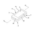
- FIG. 1 is a perspective view schematically illustrating an embodiment of a touch panel display device. Sectional drawing by the II-II line in FIG. FIG. 2 is a cross-sectional view showing a capacitive touch panel assembly of the display device of FIG. 1.
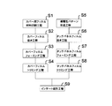
- FIG. 4 is a manufacturing process diagram showing a flow of manufacturing the capacitive touch panel assembly of FIG. 3;
- FIG. 7 is a simplified view for explaining a cover film material printing step in the manufacturing step of FIG. 4;
- the simplification figure for demonstrating a cover film extraction process.
- the simplification figure for explaining a cover film trimming process The figure which shows the film material for touch panels used for the manufacturing process of FIG. 4 simply.
- FIG. 7 is a simplified view for illustrating a state in which the second intermediate cover film is attached to the concave molding die and the second intermediate touch panel film is attached to the convex molding die in the insert molding step in the manufacturing process of FIG. 4;
- the manufacturing-process figure which shows the other example of the flow of manufacture of an electrostatic capacitance type touch panel assembly.
- FIG. 10 is a perspective view schematically showing another embodiment of the touch panel display device.
- FIG. 10 is a perspective view schematically showing another embodiment of the touch panel display device.
- the present invention is applied to a liquid crystal display device as a display device, but the present invention can be similarly applied to display devices of other forms such as an organic EL display device.
- the liquid crystal display device 2 shown in the figure includes a rectangular display device main body 3, and a display window 5 is provided on the surface (upper surface in FIG. 1) of the display device main body 3. It applies to the terminal etc.
- the liquid crystal display device 2 includes a rectangular device housing 4 having an open upper surface, the liquid crystal display means 6 is built in the device housing 4, and a capacitive touch panel assembly is provided on the surface side of the liquid crystal display means 6.
- a capacitive touch panel assembly 8 is mounted so as to cover the top opening of the device housing 4.
- the liquid crystal display means 6 may be known per se for displaying various information.
- the illustrated capacitive touch panel assembly 8 includes a capacitive touch panel 10, a resin layer 12, and an exterior cover 14.
- the capacitive touch panel 10 is configured of a touch panel film
- the first electrode pad 15M (FIGS. 9 to 10) is substantially entirely on one side (for example, the upper surface in FIGS. 2 and 3) of the touch panel film. 13) are provided in a matrix
- the first electrode pads 15M are positioned, for example, in the lateral direction (horizontal direction in FIGS. 9 to 12) based on the change in charge when the input operation is performed with a finger or the like of the hand.
- the second electrode pads 17M see FIG.
- the second electrode pads 17M are provided in a matrix form substantially over the other surface (the lower surface in FIG. 2), the second electrode pads 17M are subjected to an input operation using a finger or the like. Based on the change in charge, for example, the position in the vertical direction (vertical direction in FIGS. 9 to 13) is detected, and the electrostatic capacitance is detected based on the detected positions of the first and second electrode pads 15M and 17M. It is possible to detect the input operation position of the mold touch panel 10.
- the touch panel film of the capacitive touch panel 10 is formed of a transparent to translucent resin material, such as polyethylene terephthalate (PET), polycarbonate (PC), acrylic resin, etc., and the first and second electrode pads 15M and 17M are It is formed of a transparent conductive material such as indium tin oxide (ITO), polyethylenedioxyphene (PEDOT) as a conductive polymer which is an alternative to ITO, silver nanowire ink, silver halide particles and the like.
- a transparent to translucent resin material such as polyethylene terephthalate (PET), polycarbonate (PC), acrylic resin, etc.
- ITO indium tin oxide
- PEDOT polyethylenedioxyphene
- the capacitive touch panel 10 in which the first electrode pad 15M is provided on one side of the touch panel film and the second electrode pad 17M is provided on the other side is used.
- the first electrode pad may be provided in the first specific area on one side of the touch panel film, and the second electrode pad may be provided in another second specific area on this side, or one side of the touch panel film may be used.
- the first electrode pad may be provided, and the second electrode pad may be provided on the surface side of the first electrode pad via the electrically insulating layer.
- this capacitive touch panel 10 has a top wall 16 covering the surface side of the liquid crystal display means 6 and a circumferential side wall 18 extending from the outer peripheral portion of the top wall 16 to the liquid crystal display means 6 side.
- An extension 19 extends from a portion of the circumferential side wall 18 (the side wall 18a shown on the left side in FIG. 2).
- the first and second electrode pads 15M and 17M are provided on substantially the entire area of the top wall 16 of the capacitive touch panel 10, as will be understood from the description to be described later, and the circumferential side walls thereof.
- the first and second connection terminals (electrical connection portions) 15T and 17T electrically connected to the first and second electrode pads 15M and 17M are also provided in the extension portion 19 (see FIG. 10).
- the first and second connection terminals 15T and 17T are connected to a control substrate (not shown) of the liquid crystal display device 2. Therefore, it is possible to detect the position of a finger or the like who has performed an input operation and the movement of the finger by using the change in charge on the top wall 16 and the circumferential wall 18 of the capacitive touch panel 10.
- Such first and second electrode pads 15M and 17M do not need to be provided substantially over the entire area of the ceiling wall 16 and the circumferential side wall 18, and the top wall 16 corresponding to the input operation unit operated by a finger or the like. It may be provided on a part and part of the circumferential side wall 18, and even with this configuration, the desired effects described later can be achieved.
- the exterior cover 14 is formed of a cover film, has a rectangular shape corresponding to the shape of the device housing 4, and covers the top wall 20 covering the surface side of the top wall 16 of the capacitive touch panel 10. And a peripheral side wall 22 extending from the outer peripheral portion to the liquid crystal display means 6 side.
- the outer shape of the outer cover 14 is somewhat larger than the outer shape of the capacitive touch panel 10, and the resin layer 12 is interposed between the outer cover 14 (cover film) and the capacitive touch panel 10 (touch panel film). Ru.
- the resin layer 12 is formed by pouring a molten resin into the gap between the exterior cover 14 (cover film) and the capacitive touch panel 10 (touch panel film).
- the cover film of the exterior cover 14 is formed of a transparent to translucent resin material, such as polyethylene terephthalate (PET), polycarbonate (PC), acrylic resin, etc., similarly to the capacitive touch panel 10.
- a transparent to translucent resin material such as polyethylene terephthalate (PET), polycarbonate (PC), acrylic resin, etc.
- an opening area 24 (functioning as an input operation unit) is formed in a predetermined area of the inner surface of the exterior cover 14 (specifically, substantially the entire outer peripheral edge of the ceiling wall 20 and the entire peripheral wall 22).
- a printing layer 26 is provided. Accordingly, an open area 24 defined by the printing layer 26 is exposed from the outside of the exterior cover 14, and the open area 24 functions as the display window 5 of the liquid crystal display device 2. Thus, the capacitive touch panel 10 is operated to input.
- resin (resin of resin layer 12) used for insert molding transparent or translucent resin material, for example, acrylic resin, polycarbonate (PC), ABS resin etc. can be used.
- the exterior cover 14 (cover film) and the capacitive touch panel 10 (touch panel film) are manufactured prior to performing insert molding.
- printing is performed on one side of the transparent to translucent cover film material 32 to form the print layer 26 (cover film material printing step S ⁇ b> 1).
- cover film material 32 as described above, for example, a film of polyethylene terephthalate (PET) can be used.
- PET polyethylene terephthalate
- the cover film material printing step S1 as shown in FIG. 5, for example, printing of black, white, metallic tone, etc. is performed on a substantially rectangular annular predetermined area 34 which is somewhat larger than the top wall 20 of the exterior cover 14. And print in this manner to form a transparent to semitransparent rectangular opening area 24 at the center of the predetermined area 34, and this opening area 24 is a window of the exterior cover 14 (that is, the display of the liquid crystal display device 2). Act as a window 5).
- the print layer 26 of a predetermined area is formed at eight places at intervals in one film material 32 for a cover, but an appropriate number corresponding to the size of the film material 32 for a cover may be used. It can be made to print at one time.
- Such a printing layer 26 can be printed by an appropriate printing method such as screen printing or offset printing.
- cover film material 32 is punched to form the cover film piece 36 including the predetermined area 34 (cover film extraction step S2), and the thus-formed cover film becomes a cover film having the opening area 24. .
- this cover film removing step S2 for example, it can be performed by die cutting using a press die (not shown) or the like, and by die cutting as shown by a dashed dotted line 40 in FIG. A cover film piece 36 shown in FIG.
- cover film piece 36 shown in FIG. 6 is subjected to forming processing to form a first intermediate cover film 52 shown in FIG. 7 (cover film forming step S3).
- the cover film piece 36 is preheated to a predetermined temperature range, and the cover film piece 36 thus heated is set in a press die (not shown) and subjected to a forming process using a press die. That is, a convex forming die and a concave forming die are used as a press die, and a cover film piece 36 is interposed between both forming dies, and forming is performed by the convex forming die and the concave forming die, By this processing, the first intermediate cover film 52 having the shape shown in FIG. 7 is formed.
- This forming process can be processed by vacuum forming, pressure forming, or a combination thereof in addition to the above-described heat press forming.
- the first intermediate cover film 52 has a rising portion 54 extending upward (a portion corresponding to the circumferential side wall 22 of the exterior cover 14) and a flat portion 56 extending in a planar manner inward from the upper end portion of the rising portion 54.
- the predetermined area 34 provided with the print layer 26 includes the rising portion 54 and the annular flange 58 extending outward from the lower end portion of the rising portion 54). It extends to the outer peripheral edge of the flat portion 56 following the rising portion 54.
- trimming processing is performed on the first intermediate cover film 52 shown in FIG. 7 to remove unnecessary portions, and the second intermediate cover film 60 as shown in FIG. 8 is formed (cover film trimming step S4). Also in the cover film trimming step S4, similarly to the cover film removing step S2, for example, using a press die (not shown) or the like, the first intermediate cover film 52 is die-cut by this press die, and outward The second intermediate cover film 60 shown in FIG.
- the second intermediate cover film 60 is formed in substantially the same shape as the exterior cover 14 and has a rising portion 54 corresponding to the circumferential side wall 22 of the exterior cover 14 and a flat portion 56 corresponding to the top wall 20 thereof.
- the exterior cover 14 cover film
- the capacitive touch panel 10 can be manufactured in substantially the same manner as the exterior cover 14 as follows, for example.
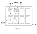
- the conductive pattern PT is formed on a transparent to semitransparent film material 62 for a touch panel.
- the conductive pattern PT includes the first and second conductive patterns 15 and 17.
- the first conductive pattern 15 is formed on one side of the touch panel film material 62.
- the second conductive pattern 17 is a touch panel film material 62.
- a film material 62 for a touch panel as described above, for example, a film of polyethylene terephthalate (PET) can be used.
- PET polyethylene terephthalate
- the first conductive pattern 15 is formed on a predetermined region R (a region surrounded by a dashed dotted line 66) of one side of the film material 62 ( Only a part of the first conductive pattern 15 is shown in FIGS. As shown in FIG. 10, the first conductive pattern 15 includes a plurality of first electrode pads 15M arranged in a matrix, a plurality of first connection terminals 15T, and a plurality of second connection terminals 17T.
- the predetermined region R has a region Ra and a region Rb (the boundary between the region Ra and the region Rb is shown by a dotted line 66a), and the first electrode pad 15M is formed substantially throughout the region Ra.
- the second connection terminals 15T and 17T are arranged in a line on one end side of the region Rb.
- the second conductive pattern 17 is formed on the other surface of the predetermined region R (note that, in FIGS. 9 and 10, a part of the second conductive pattern 17 is shown).
- the second conductive pattern 17 a large number of second electrode pads 17 M formed in a matrix over substantially the entire area on the other surface side of the region Ra and a third wiring 17 Lb connected to the second electrode pads are included. Inclusion, all of which are formed of transparent conductive materials as described above.
- through holes TH are formed in predetermined places of the film material 62 for a touch panel, and filling printing using a conductive material is performed on these through holes TH, thereby forming the second wiring 17Lb and the third wiring 17Lb corresponding to the second wiring 17Lb. Connect electrically. Further, carbon printing is performed on the first and second connection terminals 15T and 17T to apply carbon ink to the first and second connection terminals 15T and 17T. As described above, by applying the carbon ink to the first and second connection terminals 15T and 17T, the first and second connection terminals 15T and 17T are protected by the carbon ink, and the occurrence of the migration phenomenon is prevented.
- the sheet-like touch panel film material 62 is used, but a roll-like touch panel film material may be used.
- all the electrical connection portions are formed on one side of the film material 62 for touch panel, the electrical connection portions are formed on both sides of the film material 62 for touch panel.
- the second connection terminal 17T and the second wiring 17La are formed on the other surface of the touch panel film material 62, and the second wiring 17La and the third wiring 17Lb are formed in the through holes TH. It may be configured to be directly connected without interposing, and the formation of the through holes TH is not necessary.
- touch panel film material 62 is punched to form a touch panel film piece 64 (touch panel film removing step S6), and the touch panel film formed in this manner becomes a touch panel film.
- this touch panel film removing step S6 for example, it can be performed by a die cutting process using a press die (not shown) or the like, and as shown by an alternate long and short dash line 66 in FIG.
- the first conductive pattern 15 is present on one side of the touch panel film piece 64, and the second conductive pattern 17 is present on the other side.
- touch panel film piece 64 shown in FIG. 11 is subjected to forming processing to form a first intermediate touch panel film 68 shown in FIG. 12 (touch panel film forming step S7).
- touch panel film forming step S7 the touch panel film piece 64 is preheated to a predetermined temperature range, and the touch panel film piece 64 thus heated is set in a press mold (not shown) and subjected to forming processing by the press mold.
- a convex forming die and a concave forming die are used as a press die, and a touch panel film piece 64 is interposed between both forming dies, and forming is performed by the convex forming die and the concave forming die, By this processing, the first intermediate touch panel film 68 having the shape shown in FIG. 12 is formed.
- This forming process can be processed by vacuum forming, pressure forming, or a combination thereof in addition to the above-described heat press forming.
- the first intermediate touch panel film 68 has a rising portion 70 (portion corresponding to the circumferential side wall 18 of the capacitive touch panel 10) extending upward and a planar shape extending in a planar manner inward from the upper end portion of the rising portion 70.
- Portion 72 portion corresponding to the top wall 16 of the capacitive touch panel 10) and an annular flange 74 extending outward from the lower end portion of the rising portion 70, and the conductive pattern PT has a rising portion 70, a flat surface
- the first and second electrode pads 15 and 17M are present on the rising portion 70 and the flat portion 70, and the first and second connection terminals 15T are formed. , 17T are present on the annular flange 74.
- trimming processing is performed on the first intermediate touch panel film 68 shown in FIG. 12 to remove unnecessary portions, and the second intermediate touch panel film 76 as shown in FIG. 13 is formed (touch panel film trimming step S8).
- touch panel film trimming step S8 similarly to the touch panel film removing step S6, for example, using a press die (not shown) or the like, the first intermediate touch panel film 68 is die-cut by this press die, and outward
- the second intermediate touch panel film 76 shown in FIG. 13 is formed by removing a part (the part where the first and second connection terminals 15T and 17T are formed) leaving the annular flange 74 extending in the middle.
- the second intermediate touch panel film 76 is formed in substantially the same shape as the capacitive touch panel 10, and has a rising portion 70 corresponding to the circumferential side wall 18 of the capacitive touch panel 10 and a planar shape corresponding to the top wall 16 thereof. A portion 72 and a residual flange 78 corresponding to the extension 19 extending from the circumferential side wall 18 are formed, and thus, the capacitive touch panel 10 (touch panel film) is formed.
- the second intermediate cover film 60 (the outer cover 14) and the second intermediate touch panel film 76 (the capacitive touch panel 10) are insert-molded using a molding die (insert molding step S9).
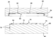
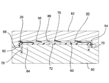
- a second intermediate touch panel film is formed on the convex portion 84 of the convex molding die 80.
- the second intermediate cover film 60 is attached to the concave portion 86 of the concave molding die 82 while mounting 76, and in a state in which these are mounted, insert molding is performed to mold the above-described capacitive touch panel assembly 8.
- the convex molding die 80 is provided with a convex portion 84 corresponding to the inner surface side shape of the second intermediate touch panel film 76, and the second intermediate touch panel film 76 is mounted so as to cover the convex portion 84. Be done.
- the convex molding die 80 is provided with a groove portion into which the lower end portion of the rising portion 70 of the second intermediate touch panel film 76 and the residual flange 78 are inserted.
- the concave molding die 82 is provided with a concave portion 86 corresponding to the outer surface shape of the second intermediate cover film 60, and the second intermediate cover film 60 is mounted so as to be fitted into the concave portion 86. .
- the convex molding die 80 to which the second intermediate touch panel film 76 is attached and the concave molding die 82 to which the second intermediate cover film 60 is attached are clamped to form an injection port (not shown).
- Molten resin is injected into the cavity 92, and the molten resin injected into the cavity 92 is cooled and solidified to insert-mold the capacitive touch panel assembly 8 described above.
- the residual flange 78 on which the first and second connection terminals 15T and 17T are formed is inserted into the groove portion provided in the convex molding die 80, the residual flange 78 is formed.
- the molten resin does not go to the (first and second connection terminals 15T and 17T), and the flexible state is maintained.
- the capacitive touch panel assembly 8 manufactured in this manner is fixed to the surface side of the liquid crystal display means 6 by, for example, an OCA tape 94 as shown in FIG. 2, and thus the capacitive touch panel assembly
- the liquid crystal display device 2 provided with 8 is manufactured.
- this electrostatic capacitance type touch panel 8 can be configured as follows.
- the other surface of the outer cover 14 is used as a functional layer
- a hard coat layer may be provided, and in order to provide an antireflective function, an antireflective layer may be provided as a functional layer on the other surface of the exterior cover 14 and an antifouling function is provided.
- an antifouling layer as a functional layer may be provided on the other surface of the exterior cover 14, and a plurality of functional layers may be provided in layers to provide these plural functions.
- Such functional layers may be carried out before the cover film material printing step S1 or the cover film material printing step S1 and the cover film removing step S2 It can be simply and easily implemented by providing a functional layer at the stage of such a cover film.
- the print layer 26 is provided on one side of the exterior cover 14 to define the opening area 24.
- a vapor deposition layer by vapor deposition is provided instead of the print layer 26.
- 24 may be defined, or a design layer (design film) having a desired design pattern or the like may be formed instead of the print layer 26 or the like or together with the print layer 26 or the like.
- the flat portion 56 (corresponding to the top wall 20), the annular rising portion 54 (corresponding to the circumferential side wall 22) and the annular flange in the cover film forming step S3.
- the first intermediate cover film 52 having the 58 is formed, it is not limited to such a configuration, and it is not necessary to form the annular rising portion 54 and the annular flange 58 in an annular shape, and some of them are cut. It can also be formed as an integral part.
- the capacitive touch panel 10 also has a flat portion 72 (corresponding to the top wall 16), an annular rising portion 70 (corresponding to the circumferential side wall 18) and an annular flange 74 in the touch panel film forming step S7.
- the intermediate touch panel film 68 is formed, it is not limited to such a configuration, and it is not necessary to form the annular rising portion 70 and the annular flange 74 in an annular shape, and some of them may be cut away. It can also be formed into
- the second intermediate cover film 60 subjected to the trimming processing for the exterior cover 14 is trimmed for the capacitive touch panel 10.
- the insert molding is performed using the second intermediate touch panel film 76 subjected to the above-described method.
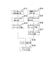
- it can be manufactured according to the manufacturing process shown in FIG.
- the first intermediate cover film 52 is manufactured by performing the cover film material printing step S 11, the cover film removing step S 12 and the cover film forming step S 13, and the capacitive touch panel 10.
- a second intermediate touch panel film 76 is manufactured by performing the conductive pattern forming step S14, the touch panel film removing step S15, the touch panel film forming step S15, and the touch panel film trimming step S17.
- the first intermediate cover film 52 after the cover film forming step S13 and the second intermediate touch panel film 76 after the touch panel film trimming step S17 are insert-molded to produce an intermediate touch panel assembly (insert molding step S18), and then the intermediate touch panel The first intermediate cover film of the assembly is trimmed to remove unnecessary portions of the first intermediate cover film 52 (cover film trimming step S19), and the capacitive touch panel assembly 10 can be manufactured in this manner as well. .
- the second intermediate cover film 60 is manufactured by performing the film material printing process for the cover, the cover film removing process, the cover film forming process, and the cover film trimming process.
- the first intermediate touch panel film 68 is manufactured by performing the conductive pattern forming process, the touch panel film removing process, and the touch panel film forming process.
- the second intermediate cover film 60 after the cover film trimming process and the first intermediate touch panel film 68 after the touch panel film forming process are insert-molded to produce an intermediate touch panel assembly (insert molding process).
- a trimming process is performed on the intermediate touch panel film to remove an unnecessary portion of the first intermediate touch panel film 68 (touch panel film trimming step), and the capacitive touch panel assembly 10 can be manufactured also in this manner.
- the manufacturing process related to the exterior cover 14 (cover film) and the capacitive touch panel 10 (touch panel film) can be improved. That is, for the exterior cover 14 (cover film), the first intermediate cover film 52 is manufactured by performing the film material printing process for the cover, the cover film removing process and the cover film forming process, and the capacitive touch panel 10 ( As for the touch panel film, the first intermediate touch panel film 68 is manufactured by performing the conductive pattern forming step, the touch panel film removing step and the touch panel film forming step. Then, the first intermediate cover film 52 after the cover film forming process and the first intermediate touch panel film 68 after the touch panel film forming process are insert-molded to produce an intermediate touch panel assembly (insert molding process).
- the cover film 52 and the first intermediate touch panel film 68 are subjected to trimming processing to simultaneously remove unnecessary portions of the first intermediate cover film 52 and the first intermediate touch panel film 68 (cover film trimming step and touch panel film trimming step)
- the capacitive touch panel assembly 10 can be manufactured.
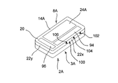
- the opening area 24 of the exterior cover 14 functions as an input operation unit (input operation screen), but the top wall 16 and the periphery of the capacitive pattern film 10 in this embodiment Since the side walls 18 are provided with the first and second electrode pads 15M and 17M in the form of a matrix, at least a part of the top wall 16 and the peripheral side surface of the capacitive touch panel 10 is used.
- at least a partial area of the circumferential side wall 22 can function as an input operation unit, and can be configured, for example, as shown in FIG.
- the first sub opening region 94 is on the right side in FIG.
- the second sub opening region 96 is provided on the lower side in FIG.
- the main opening area 24A functions as a display window and an input operation unit equivalent to the opening area 24 in the embodiment described above.
- the first sub opening area 94 is an input operation area 102 (input operation unit) provided on the side wall 22x of the exterior cover 14A (the side wall adjacent to the first sub opening area 94 and the side wall of the display device main body 3A).
- Function is provided to display the operation content of the input operation area 102, and the input operation is performed on the portion of the side wall 22x corresponding to the operation information displayed in the first sub opening area 94.
- the input operation can be detected by the change in charge on the side wall (not shown) of the capacitive touch panel (the side wall located inside the side wall 22x of the exterior cover 14A).
- notations such as symbols and figures indicating the contents of the operation may be added.
- the symbol 102 is used as an input unit such as "volume loud”, “zoom expansion”, “forward”, etc.
- the symbol 104 can be used as an input unit such as “volume reduction”, “zoom reduction”, “backward” and the like, and the symbol 106 can be used as an input unit such as “on / off of sound”.
- An LED or the like can be easily incorporated inside the operation unit, and the operation state can be visually recognized by turning on / off the operation unit.
- the first sub opening area 94 may be provided on the side wall 22 x of the exterior cover 14 A.
- the first sub opening area 94 functions as a display window and an input operation unit.
- the operation information displayed on the screen is directly input and operated from the first sub opening area 94.
- the second sub opening area 94 corresponds to an input operation area (not shown) (functioning as an input operation unit) provided on the side wall 22 y of the exterior cover 14 A (side wall adjacent to the second sub opening area 96). , And is for displaying the operation content of the input operation area, and the input operation is performed by inputting the portion of the side wall 22y corresponding to the operation information displayed in the second sub opening area 96.
- the input operation can be detected by the change in charge on the side wall (not shown) of the capacitive touch panel (the side wall located inside the side wall 22y of the exterior cover 14A).
- the second sub opening area 96 may also be provided on the side wall 22y of the exterior cover 14A.
- the second sub opening area 96 functions as a display window and an input operation unit.
- the operation information displayed in the opening area 96 is directly input and operated from the second sub opening area 96.
- the liquid crystal display device 2A since the first and second sub opening regions 94 and 96 are provided in addition to the main opening region 24A, the liquid crystal display device 2A can have more functions. The operability at the time of operating those functions can be improved, and the liquid crystal display device 2A more convenient can be provided. In addition, one or three or more sub-opening regions may be provided, and the arrangement can also be provided at an appropriate site in consideration of usage and the like.
- Such a liquid crystal display device 2A can be applied to a smartphone, a tablet terminal, a digital camera, etc., and when the touch panel operation function is provided on the side, input operation such as volume, zoom, channel switching, power ON / OFF, etc. Can be set on the side surface of the display device main body 3A without individually setting the operation button or the like.
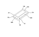
- the main opening area 24A, the first sub opening area 94, and the second sub opening area 96 are flat surfaces of the exterior cover 14A of the capacitive touch panel assembly 8A (ie, Although provided on the top wall 20 and the side walls 22x and 22y), the opening region can also be provided on a curved surface, and can be configured, for example, as shown in FIG.
- the connecting portion between the top wall 20 and the side wall 22x of the exterior cover 14B has a relatively large R shape, and the first sub opening region 94B is provided along the R shape. .
- the connecting portion between the top wall 20 and the side wall 22y has a relatively large R shape, and the second sub opening region 96B is provided along the R shape.
- the first and second sub opening regions 94B and 96B function as a display window and an input operation unit (touch panel input operation unit), and the operation information displayed in the first and second sub opening regions 94B and 96B is Direct operation is performed from the first and second sub opening regions 94B and 96B.
- the first and second sub aperture regions 94B and 96B are provided, so that the liquid crystal display device 2B can have many functions. The operability at the time of operating those functions can be improved, and a more convenient liquid crystal display device 2B can be provided. Also in this case, one or three or more sub opening regions may be provided. When the sub opening region is provided at the connecting portion between the top wall 20 and the circumferential side wall 22 as described above, the shape of the liquid crystal display means 6 may be made to correspond to the R shape of the connecting portion.
- the surface (upper surface) is formed in a flat shape, but it may be a curved surface, and / or the top wall 20 and the circumferential side wall 22.
- the connection portion with the above can also be made a relatively large R shape, regardless of the presence or absence of the sub opening region.
- the shape of the liquid crystal display device is not limited to this, and may be, for example, another shape such as a circle, an ellipse, or a polygon. It can also be done.
- Such a capacitive touch panel assembly can also be manufactured, for example, as follows, using the capacitive touch panel (after the touch panel film trimming process) manufactured as described above. .
- the exterior cover 14 (second intermediate cover film 60) and the capacitive touch panel 10 (second intermediate touch panel film 76) are simultaneously insert-molded in one step, as follows. Can also be made in one step.
- the capacitive touch panel 10 (second intermediate touch panel film 76) is attached to the convex portion of the first convex molding die, and A film having a design pattern or the like is provided on the concave portion side of the concave molding die, and in such a state, the first convex molding die and the first concave molding die are clamped to insert the capacitive touch panel 10 as an insert.
- in-mold molding in which a design pattern of a film or the like is applied to the surface of the resin layer formed by molding at the same time as this insert molding is carried out.
- the capacitive touch panel assembly can be manufactured.
- an exterior cover can be abbreviate
- the exterior cover is omitted, but the capacitive touch panel 10 (second intermediate touch panel film 76) is molded in-mold as described above and the resin layer 12 is formed on the surface thereof.
- the outer cover is formed by the above-described in-mold molding, and in-mold formed on the resin layer 12 on the surface side of the capacitive touch panel 10 via OCA (Optical Clear Adhesive) (for example, OCA tape)
- OCA Optical Clear Adhesive
- the exterior cover may be attached.
- the capacitive touch panel assembly may be manufactured by insert molding and pasting.
- the exterior cover 14 (second intermediate cover film 60) manufactured as described above (or another manufacturing method in advance) It can manufacture using the exterior cover and the electrostatic capacitance type touch panel 10 (2nd intermediate
- the capacitive touch panel 10 (second intermediate touch panel film 76) is mounted on the convex portion of the convex molding die, and the convex molding gold is thus mounted
- the mold and the concave mold are clamped, and the capacitive touch panel 10 is insert-molded to form the resin layer 12 on the surface side.
- the exterior cover 14 (second intermediate cover film 60) is attached by OCA to the surface side (surface side of the insert-molded resin layer 12) of the capacitive touch panel 10 (second intermediate touch panel film 76). Even in such a case, the capacitive touch panel assembly including the capacitive touch panel 10 can be manufactured.
- the exterior cover 14 is provided in the embodiment described above, the exterior cover 14 is not necessarily required, and the resin layer 12 can also function as the exterior cover.
- the capacitive touch panel 10 (second intermediate touch panel film 76) is mounted on the convex portion of the convex molding die, and the convex is formed in the mounted state.
- Mold mold and concave mold are clamped, and the capacitive touch panel 10 is insert molded to form the resin layer 12 on the surface side, and printing, painting on the surface side of the insert molded resin layer 12,
- a design pattern or the like may be added by secondary processing such as vapor deposition, or a functional layer (anti-scratching function, anti-reflection function, anti-staining function, etc.) may be added.
- a capacitive touch panel assembly including the capacitive touch panel 10 can be manufactured.
- the resin layer 12 is formed by insert molding on the surface side of the capacitive touch panel 10 (second intermediate touch panel film 76), but as the resin layer 12 instead of insert molding.
- a functional resin three-dimensional plate (or a resin three-dimensional sheet) may be attached to the capacitive touch panel 10 (second intermediate touch panel film 76).
- a three-dimensional resin plate (or three-dimensional resin sheet) is formed in advance three-dimensionally by molding so as to correspond to the outer shape of the capacitive touch panel 10, and formed.
- a design pattern or the like is added to, for example, the back side (or the front side) of the three-dimensional sheet), and a functional layer (such as a scratch prevention mechanism) is further added to the front side.
- a resin-made three-dimensional plate (or a resin-made three-dimensional sheet) may be attached by OCA on the surface side of the intermediate touch panel film 76), and even in this case, the static type provided with the capacitive touch panel 10 Capacitive touch panel assemblies can be manufactured.
- a resin-made three-dimensional plate (or a resin-made three-dimensional sheet) that functions as the resin layer 12 is formed in advance as described above, and this resin-made three-dimensional plate ( Alternatively, the capacitive touch panel 10 (second intermediate touch panel film 76) and the exterior cover 14 (second intermediate cover film 60) may be attached to a resin-made three-dimensional sheet.
- a resin-made three-dimensional plate (or resin-made three-dimensional sheet) is attached to the surface side of the capacitive touch panel 10 (second intermediate touch panel film 76) with OCA, and this resin-made three-dimensional plate (or The exterior cover 14 (second intermediate cover film 60) may be attached to the surface side of the resin three-dimensional sheet via the OCA, and even in this way, the capacitive touch panel assembly including the capacitive touch panel 10 Can be manufactured.
Abstract
Provided is a manufacturing method for an assembly of a capacitance type touch panel that allows easy manufacturing of a touch panel film of a predetermined shape from film materials for a capacitance type panel. The present invention includes the following steps: a touch panel film forming step (S7) for forming a first intermediate touch panel film by applying a forming process to a film material for a touch panel in which a first conductive pattern and a second conductive pattern are formed on a transparent or semi-transparent film; and a touch panel film trimming step (S8) for applying a trimming process to the first intermediate touch panel film after the touch panel film forming step (S7). In the touch panel film trimming step (S8), a second intermediate touch panel film is formed by applying a trimming process to the first intermediate touch panel film.
Description
本発明は、静電容量の変化を利用して入力操作を検知するための静電容量型タッチパネルアセンブリの製造方法に関する。また、本発明は、このような静電容量型タッチパネルアセンブリを備えた表示装置に関する。
The present invention relates to a method of manufacturing a capacitive touch panel assembly for detecting an input operation using a change in capacitance. The present invention also relates to a display device provided with such a capacitive touch panel assembly.
例えば、タッチパネル式液晶表示装置は、液晶表示手段と、この液晶表示手段の表面側に配設されたタッチパネルアセンブリとを備え、このタッチパネルアセンブリとして、静電容量型タッチパネルアセンブリを用いたものが知られている(例えば、非特許文献1参照)。
For example, a touch panel liquid crystal display device includes liquid crystal display means and a touch panel assembly disposed on the surface side of the liquid crystal display means, and as this touch panel assembly, one using a capacitive touch panel assembly is known. (See, for example, Non-Patent Document 1).
このような静電容量型タッチパネルアセンブリは、静電容量型タッチパネルと、このタッチパネルの表面側に配設された外装部材とを備え、外装部材が透明プラスチック、透明ガラスなどから形成されている。静電容量型タッチパネルは、電気的絶縁性を有する樹脂シートを備え、この樹脂シートの片面にマトリックス状に第1導電パターン(例えば、横方向の位置を検出するためのパターン)が設けられ、その他面にマトリックス状に第2導電パターン(例えば、縦方向の位置を)検出するためのパターン)が設けられ、これら第1及び第2導電パターンに微弱の電流が供給される。
Such a capacitive touch panel assembly includes a capacitive touch panel and an exterior member disposed on the surface side of the touch panel, and the exterior member is formed of transparent plastic, transparent glass, or the like. The capacitive touch panel includes a resin sheet having electrical insulation, and a first conductive pattern (for example, a pattern for detecting a lateral position) is provided in a matrix on one side of the resin sheet, and the other A second conductive pattern (for example, a pattern for detecting the position in the vertical direction) is provided in a matrix on the surface, and a weak current is supplied to the first and second conductive patterns.
このような微弱電流の供給状態において、タッチパネルアセンブリの表面(外装部材の表面)を指などで入力操作すると、タッチパネル表面の電荷が変化し、例えば、第1導電パターン側の電荷の状態を検知して横方向の位置を検出することができ、また第2導電パターン側の電荷の変化を検知して縦方向の位置を検出することができる。
When the surface of the touch panel assembly (the surface of the exterior member) is subjected to an input operation with a finger or the like in such a weak current supply state, the charge on the touch panel surface changes, for example, the charge state on the first conductive pattern side Thus, the position in the lateral direction can be detected, and the change in charge on the side of the second conductive pattern can be detected to detect the position in the vertical direction.
このような静電容量型タッチパネルアセンブリでは、タッチパネル及び外装部材がプレート状に形成されているために、外観意匠のデザインの自由度が少なく、また入力操作面もタッチパネルアセンブリの上面のみとなって操作性に優れてなく、操作性の面での改善が望まれている。また、外装部材が透明ガラスである場合、重量が重く、割れやすいという問題があり、また透明プラスチックである場合、単品毎に切削にて生産されており、生産性が低くなるという問題がある。
In such a capacitive touch panel assembly, since the touch panel and the exterior member are formed in a plate shape, the degree of freedom in design of appearance design is small, and the input operation surface is also operated only on the upper surface of the touch panel assembly It is not excellent in quality, and improvement in terms of operability is desired. Further, when the exterior member is transparent glass, there is a problem that the weight is heavy and it is easily broken, and when it is a transparent plastic, it is produced by cutting for each single product, and there is a problem that productivity is lowered.
本発明の目的は、静電容量型パネル用フィルム材料から所定形状のタッチパネルフィルムを容易に製造することができる静電容量型タッチパネルアセンブリの製造方法を提供することである。
An object of the present invention is to provide a method of manufacturing a capacitive touch panel assembly capable of easily manufacturing a touch panel film having a predetermined shape from a film material for capacitive type panel.
本発明の他の目的は、静電容量型タッチパネルの側面にも入力操作部を設けることができる静電容量型タッチパネルアセンブリの製造方法を提供することである。
Another object of the present invention is to provide a method of manufacturing a capacitive touch panel assembly in which an input operation unit can be provided also on the side surface of the capacitive touch panel.
また、本発明の更に他の目的は、静電容量型タッチパネルに関連してその構成を比較的簡単にすることができる表示装置を提供することである。
Still another object of the present invention is to provide a display device which can make its configuration relatively simple in connection with a capacitive touch panel.
本発明の請求項1に記載の静電容量型タッチパネルアセンブリの製造方法は、透明乃至半透明フィルムに導電性パターンが形成されたタッチパネル用フィルム材料にフォーミング加工を施して第1中間タッチパネルフィルムを形成するタッチパネルフィルムフォーミング工程と、前記タッチパネルフィルムフォーミング工程後の前記第1中間タッチパネルフィルムにトリミング加工を施すタッチパネルフィルムトリミング工程と、を含むことを特徴とする。
In the method of manufacturing a capacitive touch panel assembly according to claim 1 of the present invention, a first intermediate touch panel film is formed by forming a touch panel film material in which a conductive pattern is formed on a transparent or translucent film. And a touch panel film trimming step of performing trimming on the first intermediate touch panel film after the touch panel film forming step.
また、本発明の請求項2に記載の静電容量型タッチパネルアセンブリの製造方法では、前記タッチパネルフィルムトリミング工程では、前記第1中間タッチパネルフィルムにトリミング加工を施して第2中間タッチパネルフィルムを形成することを特徴とする。
In the method of manufacturing a capacitive touch panel assembly according to claim 2 of the present invention, in the touch panel film trimming step, the first intermediate touch panel film is trimmed to form a second intermediate touch panel film. It is characterized by
また、本発明の請求項3に記載の静電容量型タッチパネルアセンブリの製造方法では、凸状成形金型に前記第1又は前記第2中間タッチパネルフィルムを装着した後に、前記凸状成形金型と凹状成形金型とを型締めしてこれら両者間に規定されるキャビティに溶融樹脂を流し込んで樹脂成形を行うインサート成型工程を行うことを特徴とする。
Further, in the method of manufacturing a capacitive touch panel assembly according to a third aspect of the present invention, after the first or second intermediate touch panel film is attached to a convex molding die, the convex molding die and It is characterized in that an insert molding step is carried out in which a resin molding is carried out by pouring a molten resin into a cavity defined between the two with a concave molding die clamped.
また、本発明の請求項4に記載の静電容量型タッチパネルアセンブリの製造方法では、透明乃至半透明フィルムの片面に設けた非透明層によって規定される開口領域を有するカバー用フィルム材料にフォーミング加工を施して第1中間カバーフィルムを形成するカバーフィルムフォーミング工程と、前記カバーフィルムフォーミング工程の後に前記第1中間カバーフィルムにトリミング加工を施すカバーフィルムトリミング工程とを更に含んでいることを特徴とする。
In the method of manufacturing a capacitive touch panel assembly according to claim 4 of the present invention, a forming process is performed on a cover film material having an opening area defined by a non-transparent layer provided on one side of a transparent to translucent film. And forming a first intermediate cover film, and a cover film trimming step of trimming the first intermediate cover film after the cover film forming step. .
また、本発明の請求項5に記載の静電容量型タッチパネルアセンブリの製造方法では、前記カバーフィルムトリミング工程では、前記第1中間カバーフィルムにトリミング加工を施して第2中間カバーフィルムを形成することを特徴とする。
In the method of manufacturing a capacitive touch panel assembly according to claim 5 of the present invention, in the cover film trimming step, the first intermediate cover film is trimmed to form a second intermediate cover film. It is characterized by
また、本発明の請求項6に記載の静電容量型タッチパネルアセンブリの製造方法では、前記凹状成形型に前記第1又は前記第2中間カバーフィルムを装着し且つ前記凸状成形金型に前記第1又は第2中間タッチパネルフィルムを装着した状態にて、前記凹状成形型と前記凸状成形型とを型締めしてこれら両者間に規定されるキャビティに溶融樹脂を流し込んで樹脂成形を行うインサート成形工程を行うことを特徴とする。
In the method of manufacturing a capacitive touch panel assembly according to a sixth aspect of the present invention, the first or second intermediate cover film is mounted on the concave mold and the convex mold is mounted on the convex mold. Insert molding in which resin molding is performed by pouring a molten resin into a cavity defined between the concave mold and the convex mold in a state in which the first or second intermediate touch panel film is mounted and clamping the concave mold and the convex mold. It is characterized by performing a process.
また、本発明の請求項7に記載の静電容量型タッチパネルアセンブリの製造方法では、前記タッチパネルフィルムフォーミング工程においては、凸状フォーミング金型と凹状フォーミング金型との間に前記タッチパネル用フィルム材料を介在させてフォーミング加工を施して前記第1中間タッチパネルフィルムを形成し、前記第1中間タッチパネルフィルムは、天壁と、前記天壁の外周部から延びる側壁と、前記側壁から外方に延びるフランジを有し、前記導電性パターンは、マトリックス状に形成された第1及び第2電極パッドを含み、前記第1及び第2電極パッドは、前記第1中間タッチパネルフィルムの前記天壁及び前記側壁の少なくとも一部に配置されていることを特徴とする。
In the method of manufacturing a capacitive touch panel assembly according to claim 7 of the present invention, in the touch panel film forming step, the film material for a touch panel is formed between a convex forming die and a concave forming die. The first intermediate touch panel film is formed by interposing a forming process, and the first intermediate touch panel film includes a top wall, a side wall extending from an outer peripheral portion of the top wall, and a flange extending outward from the side wall And the conductive pattern includes first and second electrode pads formed in a matrix, and the first and second electrode pads are at least the top wall and the side wall of the first intermediate touch panel film. It is characterized in that it is arranged in part.
また、本発明の請求項8に記載の静電容量型タッチパネルアセンブリの製造方法では、透明乃至半透明フィルムの片面に設けた非透明層によって規定される開口領域を有するカバー用フィルム材料を、凸状フォーミング金型と凹状フォーミング金型との間に介在させてフォーミング加工を施すことにより第1中間カバーフィルムを形成するカバーフィルムフォーミング工程を更に含み、前記第1中間カバーフィルムは、天壁と、前記天壁の外周部から延びる側壁とを有し、前記天壁と前記側壁との接続部の少なくとも一部はR形状を有し、前記開口領域は前記R形状を有する前記接続部に位置すると共に前記第1中間タッチパネルフィルムの前記第1及び第2電極パッドの一部に対応することを特徴とする。
In the method of manufacturing a capacitive touch panel assembly according to claim 8 of the present invention, the cover film material having an open area defined by the non-transparent layer provided on one side of the transparent to translucent film is convexly formed. The method further includes a cover film forming step of forming a first intermediate cover film by forming a forming process by being interposed between a second forming mold and a second forming mold, the first intermediate cover film having a ceiling wall, The side wall extending from the outer peripheral portion of the ceiling wall, at least a part of the connecting portion between the ceiling wall and the side wall has an R shape, and the opening region is located at the connection portion having the R shape And a part of the first and second electrode pads of the first intermediate touch panel film.
また、本発明の請求項9に記載の静電容量型タッチパネルアセンブリの製造方法では、前記カバー用フィルム材料の他面には、前記カバー用フィルムに機能を持たせるための機能層が設けられていることを特徴とする。
In the method of manufacturing a capacitive touch panel assembly according to a ninth aspect of the present invention, a functional layer for causing the cover film to have a function is provided on the other surface of the cover film material. It is characterized by
また、本発明の請求項10に記載の静電容量型タッチパネルアセンブリの製造方法では、前記導電性パターンは接続端子を含み、前記接続端子にはカーボンインクが塗布されていることを特徴とする。
In the method of manufacturing a capacitive touch panel assembly according to claim 10 of the present invention, the conductive pattern includes a connection terminal, and the connection terminal is coated with carbon ink.
また、本発明の請求項11に記載のタッチパネル式表示装置は、請求項1~11のいずれかに記載の製造方法により製造された静電容量型タッチパネルアセンブリと、前記静電容量型タッチパネルアセンブリの下側に配設された表示手段と、を備えたことを特徴とする。
A touch panel display device according to claim 11 of the present invention is a capacitive touch panel assembly manufactured by the manufacturing method according to any one of claims 1 to 11, and the capacitive touch panel assembly. And display means disposed on the lower side.
更に、本発明の請求項12に記載のタッチパネル式表示装置では、表示装置本体の表面及び側面の少なくとも一部に入力操作部が設けられていることを特徴とする。
Furthermore, in the touch panel display device according to a twelfth aspect of the present invention, an input operation unit is provided on at least a part of the front surface and the side surface of the display device main body.
更に、本発明の請求項13に記載のタッチパネル式表示装置では、表示装置本体の表面と側面との接続部の少なくとも一部はR形状を有し、前記R形状を有する接続部に入力操作部が設けられていることを特徴とする。
Furthermore, in the touch panel display device according to claim 13 of the present invention, at least a part of the connection portion between the front surface and the side surface of the display device main body has an R shape, and the input operation portion to the connection portion having the R shape. Are provided.
本発明の請求項1に記載の静電容量型タッチパネルアセンブリの製造方法によれば、タッチパネル用フィルム材料にタッチパネルフォーミング加工を施して第1中間タッチパネルフィルムを形成し(タッチパネルフィルムフォーミング工程)、その後第1中間タッチパネルフィルムにタッチパネルトリミング加工を施す(タッチパネルフィルムトリミング工程)ので、静電容量型タッチパネルアセンブリに用いる所定形状の静電容量型タッチパネルを容易に形成することができる。また、このタッチパネルフォーミング工程において、例えば天壁及び側壁を有する第1中間タッチパネルフィルム形成することにより、静電容量型タッチパネルの表面及び側面を入力操作部として機能させ、側面のタッチパネル操作が可能となる。
According to the method of manufacturing a capacitive touch panel assembly according to claim 1 of the present invention, touch panel forming processing is performed on a film material for a touch panel to form a first intermediate touch panel film (touch panel film forming step), and (1) Since the touch panel trimming process is performed on the intermediate touch panel film (touch panel film trimming step), it is possible to easily form a capacitive touch panel of a predetermined shape used for the capacitive touch panel assembly. Further, in this touch panel forming process, for example, by forming the first intermediate touch panel film having the top wall and the side wall, the surface and the side surface of the capacitive touch panel can function as an input operation unit, and the touch panel operation of the side surface becomes possible. .
また、本発明の請求項2に記載の静電容量型タッチパネルアセンブリの製造方法によれば、タッチパネルフィルムトリミング工程では、第1中間タッチパネルフィルムにトリミング加工を施して第2中間タッチパネルフィルムを形成するので、所定形状の静電容量型タッチパネルを容易につくることができるとともに、この第2中間タッチパネルフィルムを用いて静電容量型タッチパネルアセンブリを容易に製作することができる。
Further, according to the method of manufacturing a capacitive touch panel assembly according to claim 2 of the present invention, in the touch panel film trimming step, the first intermediate touch panel film is trimmed to form the second intermediate touch panel film. The capacitive touch panel having a predetermined shape can be easily formed, and the capacitive touch panel assembly can be easily manufactured using the second intermediate touch panel film.
また、本発明の請求項3に記載の静電容量型タッチパネルアセンブリの製造方法によれば、凸状成形金型に第1中間タッチパネルフィルム(又は第2中間タッチパネルフィルム)を装着した状態にて凸状成形金型と凹状成形金型とを合わせてこれら両者間に溶融樹脂を流し込んで樹脂成形を行う(インサート成形工程)ので、表面側が樹脂層で覆われた静電容量型タッチパネルを容易に成型することができるとともに、その意匠のデザイン性を高めることができる。また、このように成形することによって、表面側の樹脂層と静電容量型タッチパネルとを一体化することができ、静電容量型タッチパネルアセンブリの薄型化、軽量化を図ることができる。尚、第1中間タッチパネルフィルムを用いてインサート成形を行った後は、このインサート工程の後にタッチパネルフィルムトリミング工程を行うのが望ましい。
Further, according to the method of manufacturing a capacitive touch panel assembly according to claim 3 of the present invention, the convex is formed in a state where the first intermediate touch panel film (or the second intermediate touch panel film) is attached to the convex molding die. The resin mold is formed by pouring a molten resin into a ring-shaped mold and a concave-shaped mold together and performing resin molding (insert molding step), so that the capacitive touch panel whose surface side is covered with the resin layer is easily molded It is possible to improve the design of the design. Moreover, by molding in this manner, the resin layer on the surface side and the capacitive touch panel can be integrated, and the thickness and weight of the capacitive touch panel assembly can be reduced. In addition, after performing insert molding using a 1st intermediate | middle touch-panel film, it is desirable to perform a touch-panel film trimming process after this insertion process.
また、本発明の請求項4に記載の静電容量型タッチパネルアセンブリの製造方法によれば、カバー用フィルム材料にフォーミング加工を施して第1中間カバーフィルムを形成する(カバーフィルムフォーミング工程)し、その後第1中間カバーフィルムにカバーフィルムトリミング加工を施す(カバーフィルムトリミング工程)ので、静電容量型タッチパネルアセンブリに用いる所定形状の外装カバーを容易に製作することができ、またシームレスな立体形状を持たせることができ、防塵や防水などの機能を持たせた構造がとりやすくなる。
Further, according to the method of manufacturing a capacitive touch panel assembly according to claim 4 of the present invention, the cover film material is subjected to forming processing to form a first intermediate cover film (cover film forming step), Thereafter, a cover film trimming process is applied to the first intermediate cover film (cover film trimming step), so that an exterior cover of a predetermined shape used for the capacitive touch panel assembly can be easily manufactured, and has a seamless three-dimensional shape. This makes it easy to take a structure with dust and water proofing functions.
また、本発明の請求項5に記載の静電容量型タッチパネルアセンブリの製造方法によれば、カバーフィルムトリミング工程では、第1中間カバーフィルムにトリミング加工を施して第2中間カバーフィルムを形成するので、所定形状の外装カバーを容易につくることができるとともに、この第2中間カバーフィルムを用いて静電容量型タッチパネルアセンブリを容易に製作することができる。
Further, according to the method of manufacturing a capacitive touch panel assembly according to claim 5 of the present invention, in the cover film trimming step, the first intermediate cover film is trimmed to form the second intermediate cover film. The exterior cover having a predetermined shape can be easily formed, and the capacitive touch panel assembly can be easily manufactured using this second intermediate cover film.
また、本発明の請求項6に記載の静電容量型タッチパネルアセンブリの製造方法によれば、凹状成形金型に第1中間カバーフィルム(又は第2中間カバーフィルム)を装着し且つ凸状成形金型に第1中間タッチパネルフィルム(又は第2中間タッチパネルフィルム)を装着した状態にて、凹状成形型と凸状成形型とを型締めしてこれら両者間に規定されるキャビティに溶融樹脂を流し込んで樹脂成形を行うインサート成形工程を行うので、静電容量型タッチパネルの表面側に樹脂層を介して外装カバーを設けた静電容量型タッチパネルアセンブリを容易につくることができるとともに、静電容量型タッチパネルと外装カバーとを樹脂層を介して一体化することができる。また、このようにして製作することによって、生産効率を高めることができるとともに、生産コストの低減を図ることができ、更に静電容量型タッチパネルアセンブリの更なる薄型化、軽量化を図ることができる。
Further, according to the method of manufacturing a capacitive touch panel assembly according to the sixth aspect of the present invention, the first intermediate cover film (or the second intermediate cover film) is attached to the concave molding die and the convex molding gold is With the first intermediate touch panel film (or second intermediate touch panel film) attached to the mold, the concave mold and the convex mold are clamped, and the molten resin is poured into the cavity defined therebetween. Since an insert molding process for resin molding is performed, a capacitive touch panel assembly provided with an exterior cover via a resin layer on the surface side of the capacitive touch panel can be easily formed, and a capacitive touch panel And the exterior cover can be integrated through the resin layer. In addition, by manufacturing in this manner, the production efficiency can be enhanced, the production cost can be reduced, and the thickness and weight of the capacitive touch panel assembly can be further reduced. .
尚、第1中間タッチパネルフィルム及び第2中間カバーフィルムを用いてインサート成形を行った場合、このインサート成形の後に第1中間タッチパネルフィルムをトリミング加工するタッチパネルフィルムトリミング工程を行うのが望ましく、また第2中間タッチパネルフィルム及び第1中間カバーフィルムを用いてインサート成形を行った場合、このインサート形成の後に第1中間カバーフィルムをトリミング加工するカバーフィルムトリミング工程を行うのが好ましく、更に、第1中間タッチパネルフィルム及び第1中間カバーフィルムを用いてインサート成形を行った場合、このインサート成形の後に上述のタッチパネルフィルムトリミング工程及びカバーフィルムトリミング工程を同時に行うのが望ましい。
When insert molding is performed using the first intermediate touch panel film and the second intermediate cover film, it is desirable to perform a touch panel film trimming step of trimming the first intermediate touch panel film after the insert molding, and the second When insert molding is performed using the intermediate touch panel film and the first intermediate cover film, it is preferable to perform a cover film trimming step of trimming the first intermediate cover film after the insert formation, and further, the first intermediate touch panel film And when performing insert molding using a 1st intermediate cover film, it is desirable to perform the above-mentioned touch panel film trimming process and cover film trimming process simultaneously after this insert molding.
また、本発明の請求項7に記載の静電容量型タッチパネルアセンブリの製造方法によれば、タッチパネルフィルムフォーミング工程において、凸状フォーミング金型と凹状フォーミング金型との間にタッチパネル用フィルム材料を介在させてフォーミング加工を施して第1中間タッチパネルフィルムをつくるので、フォーミング加工した第1中間タッチパネルフィルムは、天壁、側壁及びフランジを有する形状となる。そして、この第1中間タッチパネルフィルムの天壁及び側壁の少なくとも一部に第1及び第2電極パッドが配置されているので、静電容量型タッチパネルの表面及び側面の少なくとも一部を入力操作部として機能させることができ、静電容量型タッチパネルの表面に加えて側面においてもタッチパネル操作が可能となり、操作性の向上した多機能の静電容量型タッチパネルアセンブリを提供することができる。
Further, according to the method of manufacturing a capacitive touch panel assembly according to claim 7 of the present invention, in the touch panel film forming step, a film material for a touch panel is interposed between the convex forming die and the concave forming die. Since the first intermediate touch panel film is formed by forming the first intermediate touch panel film, the first intermediate touch panel film subjected to the forming process has a shape having a top wall, a side wall, and a flange. Then, since the first and second electrode pads are disposed on at least a part of the top wall and the side wall of the first intermediate touch panel film, at least a part of the surface and the side of the capacitive touch panel is used as the input operation unit The touch panel can be operated and touch panel operation can be performed also on the side surface in addition to the surface of the capacitance touch panel, and a multifunctional touch panel assembly with improved operability can be provided.
また、本発明の請求項8に記載の静電容量型タッチパネルアセンブリの製造方法によれば、第1中間カバーフィルムの天壁と側壁との接続部の少なくとも一部はR形状を有し、開口領域はR形状を有する接続部に位置すると共に第1中間タッチパネルフィルムの第1及び第2電極パッドの一部に対応するので、天壁と側壁との接続部においてもタッチパネル操作が可能となり、操作性の向上した多機能の静電容量型タッチパネルアセンブリを提供することができる。
Further, according to the method of manufacturing a capacitive touch panel assembly according to claim 8 of the present invention, at least a part of the connecting portion between the top wall and the side wall of the first intermediate cover film has an R shape and the opening Since the region is located at the connecting portion having the R shape and corresponds to a part of the first and second electrode pads of the first intermediate touch panel film, the touch panel operation becomes possible even at the connecting portion between the top wall and the side wall. It is possible to provide a multifunctional touch panel assembly with improved properties.
また、本発明の請求項9に記載の静電容量型タッチパネルアセンブリの製造方法によれば、カバー用フィルム材料の他面に機能層が設けられているので、静電容量型タッチパネルアセンブリの外装カバーに各種機能を持たせることができる。例えば、バードコート層を設けることにより、フィルムに傷付防止機能を持たせることができ、反射防止層を設けることにより、フィルムに反射防止機能を持たせることができ、また防汚層を設けることにより防汚機能を持たせることができる。尚、この機能層の付与は、インサート成形前に行うのが望ましい。
Further, according to the method of manufacturing a capacitive touch panel assembly according to claim 9 of the present invention, since the functional layer is provided on the other surface of the cover film material, the exterior cover of the capacitive touch panel assembly Can have various functions. For example, by providing a bird coat layer, the film can have a scratch preventing function, and by providing an antireflection layer, the film can have an antireflection function, and an antifouling layer can be provided. Antifouling function can be provided. In addition, it is desirable to carry out the application of this functional layer before insert molding.
また、本発明の請求項10に記載の静電容量型タッチパネルアセンブリの製造方法によれば、接続端子にはカーボンインクが塗布されているので、マイグレーション現象の発生を防止できると共に、接続端子の強度を上げてこれを保護することができる。
Further, according to the method of manufacturing a capacitive touch panel assembly according to claim 10 of the present invention, since carbon ink is applied to the connection terminal, the occurrence of the migration phenomenon can be prevented and the strength of the connection terminal can be prevented. To protect it.
また、本発明の請求項11に記載のタッチパネル式表示装置は、請求項1~10のいずれかに記載の製造方法により製造された静電容量型タッチパネルアセンブリを備えているので、静電容量型タッチパネルに関連して表示装置の軽量化、薄型化を達成することができる。
In addition, since the touch panel display device according to claim 11 of the present invention includes the capacitive touch panel assembly manufactured by the manufacturing method according to any one of claims 1 to 10, Weight reduction and thickness reduction of the display device can be achieved in relation to the touch panel.
更に、本発明の請求項12に記載のタッチパネル式表示装置によれば、表示装置本体の表面及び前記表示装置本体の側面の少なくとも一部に入力操作部が設けられているので、その表面に加えて側面にも操作機能を持たせることができ、従来に比してより多用途に適合し且つ使用勝手の向上した表示装置を提供することができる。
Furthermore, according to the touch panel display device according to claim 12 of the present invention, the input operation unit is provided on the surface of the display device main body and at least a part of the side surface of the display device main body. Thus, it is possible to provide an operation function to the side surface as well, and it is possible to provide a display device which is more versatile than before and is improved in usability.
更に、本発明の請求項13に記載のタッチパネル式表示装置によれば、表示装置本体の表面と側面との接続部に入力操作部が設けられているので、当該接続部にも操作機能を持たせることができ、従来に比してより多用途に適合し且つ使用勝手の向上した表示装置を提供することができる。
Furthermore, according to the touch panel display device of claim 13 of the present invention, since the input operation unit is provided at the connection portion between the front surface and the side surface of the display device main body, the connection portion also has an operation function. Thus, it is possible to provide a display device which is more versatile than before and is improved in usability.
以下、添付図面を参照して、本発明に従う静電容量型タッチパネルアセンブリの製造方法及びこれを備えたタッチパネル式表示装置について説明する。尚、この実施形態では、表示装置としての液晶表示装置に適用して説明するが、有機EL表示装置などの他の形態の表示装置にも同様に適用することができる。
Hereinafter, with reference to the accompanying drawings, a method of manufacturing a capacitive touch panel assembly according to the present invention and a touch panel display including the same will be described. In this embodiment, the present invention is applied to a liquid crystal display device as a display device, but the present invention can be similarly applied to display devices of other forms such as an organic EL display device.
図1及び図2において、図示の液晶表示装置2は、矩形状の表示装置本体3を備え、この表示装置本体3の表面(図1において上面)に表示窓5が設けられ、例えばスマートフォン、タブレット端末などに適用される。この液晶表示装置2は、上面が開放された矩形状の装置ハウジング4を備え、この装置ハウジング4内に液晶表示手段6が内蔵され、この液晶表示手段6の表面側に静電容量型タッチパネルアセンブリ8が配設され、この静電容量型タッチパネルアセンブリ8は、装置ハウジング4の上面開口を被うように装着されている。液晶表示手段6は各種情報を表示するためのそれ自体周知のものでよい。
1 and 2, the liquid crystal display device 2 shown in the figure includes a rectangular display device main body 3, and a display window 5 is provided on the surface (upper surface in FIG. 1) of the display device main body 3. It applies to the terminal etc. The liquid crystal display device 2 includes a rectangular device housing 4 having an open upper surface, the liquid crystal display means 6 is built in the device housing 4, and a capacitive touch panel assembly is provided on the surface side of the liquid crystal display means 6. A capacitive touch panel assembly 8 is mounted so as to cover the top opening of the device housing 4. The liquid crystal display means 6 may be known per se for displaying various information.
図3をも参照して、図示の静電容量型タッチパネルアセンブリ8は、静電容量型タッチパネル10と、樹脂層12と、外装カバー14とを備えている。静電容量型タッチパネル10は、後述するように、タッチパネルフィルムから構成され、このタッチパネルフィルムの片面(例えば、図2及び図3において上面)の実質上全域に、第1電極パッド15M(図9~図13参照)がマトリックス状に設けられ、第1電極パッド15Mは、手の指などで入力操作したときの電荷の変化に基づいて、例えば横方向(図9~図12において左右方向)の位置を検知し、その他面(図2において下面)の実質上全域に、第2電極パッド17M(図9参照)がマトリックス状に設けられ、第2電極パッド17Mは、指などで入力操作したときの電荷の変化に基づいて、例えば縦方向(図9~図13において上下方向)の位置を検知し、第1及び第2電極パッド15M,17Mの検知位置に基づいて、静電容量型タッチパネル10の入力操作位置を検出することができる。
Referring also to FIG. 3, the illustrated capacitive touch panel assembly 8 includes a capacitive touch panel 10, a resin layer 12, and an exterior cover 14. As described later, the capacitive touch panel 10 is configured of a touch panel film, and the first electrode pad 15M (FIGS. 9 to 10) is substantially entirely on one side (for example, the upper surface in FIGS. 2 and 3) of the touch panel film. 13) are provided in a matrix, and the first electrode pads 15M are positioned, for example, in the lateral direction (horizontal direction in FIGS. 9 to 12) based on the change in charge when the input operation is performed with a finger or the like of the hand. When the second electrode pads 17M (see FIG. 9) are provided in a matrix form substantially over the other surface (the lower surface in FIG. 2), the second electrode pads 17M are subjected to an input operation using a finger or the like. Based on the change in charge, for example, the position in the vertical direction (vertical direction in FIGS. 9 to 13) is detected, and the electrostatic capacitance is detected based on the detected positions of the first and second electrode pads 15M and 17M. It is possible to detect the input operation position of the mold touch panel 10.
静電容量型タッチパネル10のタッチパネルフィルムは、透明乃至半透明の樹脂材料、例えばポリエチレンテレフタレート(PET)、ポリカーボネート(PC)、アクリル樹脂などから形成され、第1及び第2電極パッド15M,17Mは、透明導電性材料、例えば酸化インジウムスズ(ITO)、ITO代替素材である導電性高分子のポリエチレンジオキシオフェン(PEDOT)、銀ナノワイヤーインク、ハロゲン化銀粒子などから形成される。
The touch panel film of the capacitive touch panel 10 is formed of a transparent to translucent resin material, such as polyethylene terephthalate (PET), polycarbonate (PC), acrylic resin, etc., and the first and second electrode pads 15M and 17M are It is formed of a transparent conductive material such as indium tin oxide (ITO), polyethylenedioxyphene (PEDOT) as a conductive polymer which is an alternative to ITO, silver nanowire ink, silver halide particles and the like.
この実施形態では、タッチパネルフィルムの片面に第1電極パッド15Mを設け、その他面に第2電極パッド17Mを設けた静電容量型タッチパネル10を用いているが、このような形態のものに限定されず、タッチパネルフィルムの片面の第1特定領域に第1電極パッドを設け、この片面の他の第2特定領域に第2電極パッドを設けたものを用いるようにしてもよく、或いはタッチパネルフィルムの片面に第1電極パッドを設けるとともに、この第1電極パッドの表面側に電気的絶縁層を介して第2電極パッドを設けたものを用いるようにしてもよい。
In this embodiment, the capacitive touch panel 10 in which the first electrode pad 15M is provided on one side of the touch panel film and the second electrode pad 17M is provided on the other side is used. Alternatively, the first electrode pad may be provided in the first specific area on one side of the touch panel film, and the second electrode pad may be provided in another second specific area on this side, or one side of the touch panel film may be used. The first electrode pad may be provided, and the second electrode pad may be provided on the surface side of the first electrode pad via the electrically insulating layer.
この静電容量型タッチパネル10は、後に説明するように、液晶表示手段6の表面側を覆う天壁16と、この天壁16の外周部から液晶表示手段6側に延びる周側壁18とを有し、周側壁18の一部(図2において左側に示す側壁18a)から延長部19が延びている。この形態では、第1及び第2電極パッド15M,17Mは、後述する記載から理解されるように、静電容量型タッチパネル10の天壁16の実質上全域に設けられているとともに、その周側壁18にも設けられ、またその延長部19には第1及び第2電極パッド15M,17Mに電気的に接続された第1及び第2接続端子(電気的接続部)15T,17T(図10参照)が設けられ、この第1及び第2接続端子15T,17Tは、液晶表示装置2の制御基板(図示せず)に接続される。従って、静電容量タッチパネル10の天壁16及び周側壁18における電荷の変化を利用して、入力操作した指などの位置及び指の動きを検知することが可能となる。
As will be described later, this capacitive touch panel 10 has a top wall 16 covering the surface side of the liquid crystal display means 6 and a circumferential side wall 18 extending from the outer peripheral portion of the top wall 16 to the liquid crystal display means 6 side. An extension 19 extends from a portion of the circumferential side wall 18 (the side wall 18a shown on the left side in FIG. 2). In this embodiment, the first and second electrode pads 15M and 17M are provided on substantially the entire area of the top wall 16 of the capacitive touch panel 10, as will be understood from the description to be described later, and the circumferential side walls thereof. The first and second connection terminals (electrical connection portions) 15T and 17T electrically connected to the first and second electrode pads 15M and 17M are also provided in the extension portion 19 (see FIG. 10). , And the first and second connection terminals 15T and 17T are connected to a control substrate (not shown) of the liquid crystal display device 2. Therefore, it is possible to detect the position of a finger or the like who has performed an input operation and the movement of the finger by using the change in charge on the top wall 16 and the circumferential wall 18 of the capacitive touch panel 10.
尚、このような第1及び第2電極パッド15M,17Mは、天壁16及び周側壁18の実質上全域に設ける必要はなく、指などで入力操作する入力操作部に対応する天壁16の一部及び周側壁18の一部に設けるようにしてもよく、このように構成しても、後述する所望の効果を達成することができる。
Such first and second electrode pads 15M and 17M do not need to be provided substantially over the entire area of the ceiling wall 16 and the circumferential side wall 18, and the top wall 16 corresponding to the input operation unit operated by a finger or the like. It may be provided on a part and part of the circumferential side wall 18, and even with this configuration, the desired effects described later can be achieved.
また、外装カバー14は、カバーフィルムから構成され、装置ハウジング4の形状に対応した矩形状であり、静電容量型タッチパネル10の天壁16の表面側を覆う天壁20と、この天壁20の外周部から液晶表示手段6側に延びる周側壁22とを有している。この外装カバー14の外形は、静電容量型タッチパネル10の外形よりも幾分大きく、外装カバー14(カバーフィルム)と静電容量型タッチパネル10(タッチパネルフィルム)との間に樹脂層12が介在される。この実施形態では、後に説明するように、外装カバー14(カバーフィルム)と静電容量型タッチパネル10(タッチパネルフィルム)との間の間隙に溶融樹脂を流し込んで樹脂層12が形成される。
Further, the exterior cover 14 is formed of a cover film, has a rectangular shape corresponding to the shape of the device housing 4, and covers the top wall 20 covering the surface side of the top wall 16 of the capacitive touch panel 10. And a peripheral side wall 22 extending from the outer peripheral portion to the liquid crystal display means 6 side. The outer shape of the outer cover 14 is somewhat larger than the outer shape of the capacitive touch panel 10, and the resin layer 12 is interposed between the outer cover 14 (cover film) and the capacitive touch panel 10 (touch panel film). Ru. In this embodiment, as described later, the resin layer 12 is formed by pouring a molten resin into the gap between the exterior cover 14 (cover film) and the capacitive touch panel 10 (touch panel film).
この外装カバー14のカバーフィルムは、静電容量型タッチパネル10と同様に、透明乃至半透明の樹脂材料、例えばポリエチレンテレフタレート(PET)、ポリカーボネート(PC)、アクリル樹脂などから形成される。
The cover film of the exterior cover 14 is formed of a transparent to translucent resin material, such as polyethylene terephthalate (PET), polycarbonate (PC), acrylic resin, etc., similarly to the capacitive touch panel 10.
この形態では、外装カバー14の内面の所定領域(具体的には、天壁20の外周縁部及び周側壁22の実質上全域)に、開口領域24(入力操作部として機能する)を形成するための印刷層26が設けられている。従って、この外装カバー14の外側からは、印刷層26によって規定される開口領域24が露呈し、この開口領域24が液晶表示装置2の表示窓5として機能し、かかる開口領域24を介して指などによって静電容量型タッチパネル10を入力操作するようになる。
In this embodiment, an opening area 24 (functioning as an input operation unit) is formed in a predetermined area of the inner surface of the exterior cover 14 (specifically, substantially the entire outer peripheral edge of the ceiling wall 20 and the entire peripheral wall 22). A printing layer 26 is provided. Accordingly, an open area 24 defined by the printing layer 26 is exposed from the outside of the exterior cover 14, and the open area 24 functions as the display window 5 of the liquid crystal display device 2. Thus, the capacitive touch panel 10 is operated to input.
インサート成形に用いる樹脂(樹脂層12の樹脂)としては、透明乃至半透明の樹脂材料、例えば、アクリル樹脂、ポリカーボネート(PC)、ABS樹脂などを用いることができる。
As resin (resin of resin layer 12) used for insert molding, transparent or translucent resin material, for example, acrylic resin, polycarbonate (PC), ABS resin etc. can be used.
次に、図4とともに図5~図15を参照して、上述した静電容量型タッチパネルアセンブリ8の製造方法について説明する。尚、以下の説明においては、図1~図3と同じ部材には同一の参照番号を付して説明する。
Next, a method of manufacturing the above-described capacitive touch panel assembly 8 will be described with reference to FIGS. 5 to 15 together with FIG. In the following description, the same members as those in FIGS. 1 to 3 are described with the same reference numerals.
図4において、静電容量タッチパネルアセンブリ8を製作するには、インサート成形を行うに先立って、外装カバー14(カバーフィルム)及び静電容量型タッチパネル10(タッチパネルフィルム)を製作する。外装カバー14を製作するには、透明乃至半透明のカバー用フィルム材料32の片面に印刷を施して印刷層26を形成する(カバー用フィルム材料印刷工程S1)。例えば、カバー用フィルム材料32としては、上述したように、例えばポリエチレンテレフタレート(PET)のフィルムなどを用いることができる。このカバー用フィルム材料印刷工程S1では、図5に示すように、外装カバー14の天壁20よりも幾分大きい略矩形環状の所定領域34に、例えば、黒色、白色、メタリック調などの印刷を施し、このように印刷を施して所定領域34の中央部に透明乃至半透明の矩形状の開口領域24を形成し、この開口領域24が外装カバー14の窓(即ち、液晶表示装置2の表示窓5)として機能する。
In FIG. 4, in order to manufacture the capacitive touch panel assembly 8, the exterior cover 14 (cover film) and the capacitive touch panel 10 (touch panel film) are manufactured prior to performing insert molding. In order to manufacture the exterior cover 14, printing is performed on one side of the transparent to translucent cover film material 32 to form the print layer 26 (cover film material printing step S <b> 1). For example, as the cover film material 32, as described above, for example, a film of polyethylene terephthalate (PET) can be used. In the cover film material printing step S1, as shown in FIG. 5, for example, printing of black, white, metallic tone, etc. is performed on a substantially rectangular annular predetermined area 34 which is somewhat larger than the top wall 20 of the exterior cover 14. And print in this manner to form a transparent to semitransparent rectangular opening area 24 at the center of the predetermined area 34, and this opening area 24 is a window of the exterior cover 14 (that is, the display of the liquid crystal display device 2). Act as a window 5).
この実施形態では、一つのカバー用フィルム材料32に、間隔をおいて8箇所に所定領域の印刷層26を形成しているが、このカバー用フィルム材料32の大きさに対応した適宜の数を一度に印刷するようにすることができる。尚、このような印刷層26は、スクリーン印刷、オフセット印刷などの適宜の印刷方式によって印刷することができる。
In this embodiment, the print layer 26 of a predetermined area is formed at eight places at intervals in one film material 32 for a cover, but an appropriate number corresponding to the size of the film material 32 for a cover may be used. It can be made to print at one time. Such a printing layer 26 can be printed by an appropriate printing method such as screen printing or offset printing.
次に、カバー用フィルム材料32に抜き加工を施して所定領域34を含むカバーフィルム片36を形成し(カバーフィルム抜き工程S2)、このように形成したものが開口領域24を有するカバーフィルムとなる。
Next, the cover film material 32 is punched to form the cover film piece 36 including the predetermined area 34 (cover film extraction step S2), and the thus-formed cover film becomes a cover film having the opening area 24. .
このカバーフィルム抜き工程S2においては、例えば、プレス型(図示せず)などを用いた型抜き加工で行うことができ、図5に一点鎖線40で示すように型抜き加工することによって、図6に示すカバーフィルム片36が形成される。
In this cover film removing step S2, for example, it can be performed by die cutting using a press die (not shown) or the like, and by die cutting as shown by a dashed dotted line 40 in FIG. A cover film piece 36 shown in FIG.
その後、図6に示すカバーフィルム片36にフォーミング加工を施して図7に示す第1中間カバーフィルム52を形成する(カバーフィルムフォーミング工程S3)。このカバーフィルムフォーミング工程S3においては、カバーフィルム片36を所定温度範囲にプレヒートし、このように加熱したカバーフィルム片36をプレス型(図示せず)にセットし、プレス型によるフォーミング加工を施す。即ち、プレス型として凸状フォーミング金型及び凹状フォーミング金型を用い、これら両フォーミング金型の間にカバーフィルム片36を介在させ、凸状フォーミング金型及び凹状フォーミング金型によってフォーミング加工を施し、かく加工することによって、図7に示す形状の第1中間カバーフィルム52が形成される。このフォーミング加工は上記の熱プレス成形の他に真空成形、圧空成形、もしくはこれらの組み合わせにより加工することができる。
Thereafter, the cover film piece 36 shown in FIG. 6 is subjected to forming processing to form a first intermediate cover film 52 shown in FIG. 7 (cover film forming step S3). In the cover film forming step S3, the cover film piece 36 is preheated to a predetermined temperature range, and the cover film piece 36 thus heated is set in a press die (not shown) and subjected to a forming process using a press die. That is, a convex forming die and a concave forming die are used as a press die, and a cover film piece 36 is interposed between both forming dies, and forming is performed by the convex forming die and the concave forming die, By this processing, the first intermediate cover film 52 having the shape shown in FIG. 7 is formed. This forming process can be processed by vacuum forming, pressure forming, or a combination thereof in addition to the above-described heat press forming.
この第1中間カバーフィルム52は、上方に延びる立上り部54(外装カバー14の周側壁22に対応する部分)と、この立上り部54の上端部から内方に平面状に延びる平面状部56(外装カバー14の天壁20に対応する部分)と、立上り部54の下端部から外方に延びる環状フランジ58とを有し、印刷層26が設けられた所定領域34は、立上り部54及びこの立上り部54に続く平面状部56の外周縁部まで延びている。
The first intermediate cover film 52 has a rising portion 54 extending upward (a portion corresponding to the circumferential side wall 22 of the exterior cover 14) and a flat portion 56 extending in a planar manner inward from the upper end portion of the rising portion 54. The predetermined area 34 provided with the print layer 26 includes the rising portion 54 and the annular flange 58 extending outward from the lower end portion of the rising portion 54). It extends to the outer peripheral edge of the flat portion 56 following the rising portion 54.
次に、図7に示す第1中間カバーフィルム52にトリミング加工を施して不要な部分を除去して、図8に示す通りの第2中間カバーフィルム60を形成する(カバーフィルムトリミング工程S4)。このカバーフィルムトリミング工程S4においても、カバーフィルム抜き工程S2と同様に、例えば、プレス型(図示せず)などを用い、このプレス型によって型抜き加工を第1中間カバーフィルム52に施し、外方に延びる環状フランジ58を除去することによって、図8に示す第2中間カバーフィルム60が形成される。
Next, trimming processing is performed on the first intermediate cover film 52 shown in FIG. 7 to remove unnecessary portions, and the second intermediate cover film 60 as shown in FIG. 8 is formed (cover film trimming step S4). Also in the cover film trimming step S4, similarly to the cover film removing step S2, for example, using a press die (not shown) or the like, the first intermediate cover film 52 is die-cut by this press die, and outward The second intermediate cover film 60 shown in FIG.
この第2中間カバーフィルム60は、外装カバー14とほぼ同じ形状に形成され、外装カバー14の周側壁22に対応する立上り部54及びその天壁20に対応する平面状部56を有し、このようにして外装カバー14(カバーフィルム)が形成される。
The second intermediate cover film 60 is formed in substantially the same shape as the exterior cover 14 and has a rising portion 54 corresponding to the circumferential side wall 22 of the exterior cover 14 and a flat portion 56 corresponding to the top wall 20 thereof. Thus, the exterior cover 14 (cover film) is formed.
また、静電容量型タッチパネル10は、外装カバー14と略同様にして、例えば次のようにして製作することができる。静電容量型タッチパネル10を製作するには、まず、透明乃至半透明のタッチパネル用フィルム材料62に導電性パターンPTを形成する。この導電性パターンPTは第1及び第2導電性パターン15,17を含み、第1導電性パターン15はタッチパネル用フィルム材料62の片面に形成され、第2導電性パターン17はタッチパネル用フィルム材料62の他面に形成される(導電性パターン形成工程S5)。例えば、タッチパネル用フィルム材料62としては、上述したように、例えばポリエチレンテレフタレート(PET)のフィルムなどを用いることができる。
The capacitive touch panel 10 can be manufactured in substantially the same manner as the exterior cover 14 as follows, for example. In order to manufacture the capacitive touch panel 10, first, the conductive pattern PT is formed on a transparent to semitransparent film material 62 for a touch panel. The conductive pattern PT includes the first and second conductive patterns 15 and 17. The first conductive pattern 15 is formed on one side of the touch panel film material 62. The second conductive pattern 17 is a touch panel film material 62. Formed on the other surface (conductive pattern forming step S5). For example, as the film material 62 for a touch panel, as described above, for example, a film of polyethylene terephthalate (PET) can be used.
この導電性パターン形成工程S5では、まず、図9に示すように、このフィルム材料62の片面の所定領域R(一点鎖線66で囲まれた領域)に第1導電性パターン15が形成される(図9~図13において、第1導電性パターン15の一部のみを示す)。図10に示す様に、この第1導電性パターン15には、マトリックス状に配列された多数の第1電極パッド15Mと、複数個の第1接続端子15Tと、複数個の第2接続端子17Tと、第1電極パッド15Mと接続端子15Tとを接続する複数本の第1配線15Lと、複数個の接続端子17Tの各々に接続された複数本の第2配線17Laとが含まれ、これらは全て上述したような透明導電性材料で形成される。また、所定領域Rは領域Raと領域Rbとを有し(領域Raと領域Rbとの境界を点線66aで示す)、第1電極パッド15Mは、領域Raの実質上全域に形成され、第1及び第2接続端子15T,17Tは、領域Rbの一端側に一列に配列されて形成される。
In the conductive pattern forming step S5, first, as shown in FIG. 9, the first conductive pattern 15 is formed on a predetermined region R (a region surrounded by a dashed dotted line 66) of one side of the film material 62 ( Only a part of the first conductive pattern 15 is shown in FIGS. As shown in FIG. 10, the first conductive pattern 15 includes a plurality of first electrode pads 15M arranged in a matrix, a plurality of first connection terminals 15T, and a plurality of second connection terminals 17T. And a plurality of first wires 15L connecting the first electrode pads 15M and the connection terminals 15T, and a plurality of second wires 17La connected to the plurality of connection terminals 17T, respectively, All are formed of the transparent conductive material as described above. The predetermined region R has a region Ra and a region Rb (the boundary between the region Ra and the region Rb is shown by a dotted line 66a), and the first electrode pad 15M is formed substantially throughout the region Ra. The second connection terminals 15T and 17T are arranged in a line on one end side of the region Rb.
次に、所定領域Rの他面に第2導電性パターン17が形成される(尚、図9及び図10において、第2導電性パターン17の一部を示す)。この第2導電性パターン17には、領域Raの他面側の実質上全域にマトリックス状に形成された多数の第2電極パッド17Mと、第2電極パッドに接続された第3配線17Lbとが含まれ、これらは全て上述したような透明導電性材料で形成される。
Next, the second conductive pattern 17 is formed on the other surface of the predetermined region R (note that, in FIGS. 9 and 10, a part of the second conductive pattern 17 is shown). In the second conductive pattern 17, a large number of second electrode pads 17 M formed in a matrix over substantially the entire area on the other surface side of the region Ra and a third wiring 17 Lb connected to the second electrode pads are included. Inclusion, all of which are formed of transparent conductive materials as described above.
次に、タッチパネル用フィルム材料62の所定箇所に貫通孔THを形成し、これら貫通孔THに導電性材料を用いた充填印刷を施すことにより、第2配線17Lbと対応する第3配線17Lbとを電気的に接続する。また、第1及び第2接続端子15T,17Tにカーボン印刷を行うことにより、第1及び第2接続端子15T,17Tにカーボンインクを塗布する。このように、第1及び第2接続端子15T,17Tにカーボンインクを塗布することにより、第1及び第2接続端子15T,17Tがカーボンインクにより保護され、マイグレーション現象の発生が防止される。
Next, through holes TH are formed in predetermined places of the film material 62 for a touch panel, and filling printing using a conductive material is performed on these through holes TH, thereby forming the second wiring 17Lb and the third wiring 17Lb corresponding to the second wiring 17Lb. Connect electrically. Further, carbon printing is performed on the first and second connection terminals 15T and 17T to apply carbon ink to the first and second connection terminals 15T and 17T. As described above, by applying the carbon ink to the first and second connection terminals 15T and 17T, the first and second connection terminals 15T and 17T are protected by the carbon ink, and the occurrence of the migration phenomenon is prevented.
尚、この実施形態では、シート状のタッチパネル用フィルム材料62を用いているが、ロール状のタッチパネル用フィルム材料を用いるようにしてもよい。また、ここではタッチパネル用フィルム材料62の片面に全ての電気的接続部(第1及び第2接続端子15T,17T)を形成する構成としているが、タッチパネル用フィルム材料62の両面に電気的接続部を形成することもでき、この場合には第2接続端子17Tと第2配線17Laとをタッチパネル用フィルム材料62の他面に形成し、第2配線17Laと第3配線17Lbとを貫通孔THを介さずに直接的に接続させる構成とすれば良く、貫通孔THの形成は不要となる。
In this embodiment, the sheet-like touch panel film material 62 is used, but a roll-like touch panel film material may be used. Further, although here, all the electrical connection portions (first and second connection terminals 15T and 17T) are formed on one side of the film material 62 for touch panel, the electrical connection portions are formed on both sides of the film material 62 for touch panel In this case, the second connection terminal 17T and the second wiring 17La are formed on the other surface of the touch panel film material 62, and the second wiring 17La and the third wiring 17Lb are formed in the through holes TH. It may be configured to be directly connected without interposing, and the formation of the through holes TH is not necessary.
次に、タッチパネル用フィルム材料62に抜き加工を施してタッチパネルフィルム片64を形成し(タッチパネルフィルム抜き工程S6)、このように形成したものがタッチパネルフィルムとなる。
Next, the touch panel film material 62 is punched to form a touch panel film piece 64 (touch panel film removing step S6), and the touch panel film formed in this manner becomes a touch panel film.
このタッチパネルフィルム抜き工程S6においては、例えば、プレス型(図示せず)などを用いた型抜き加工で行うことができ、図9に一点鎖線66で示すように型抜き加工することによって、図11に示すタッチパネルフィルム片64が形成され、第1導電性パターン15は、このタッチパネルフィルム片64の片面に存在し、第2導電性パターン17は、その他面に存在する。
In this touch panel film removing step S6, for example, it can be performed by a die cutting process using a press die (not shown) or the like, and as shown by an alternate long and short dash line 66 in FIG. The first conductive pattern 15 is present on one side of the touch panel film piece 64, and the second conductive pattern 17 is present on the other side.
その後、図11に示すタッチパネルフィルム片64にフォーミング加工を施して図12に示す第1中間タッチパネルフィルム68を形成する(タッチパネルフィルムフォーミング工程S7)。このタッチパネルフィルムフォーミング工程S7においては、タッチパネルフィルム片64を所定温度範囲にプレヒートし、このように加熱したタッチパネルフィルム片64をプレス型(図示せず)にセットし、プレス型によるフォーミング加工を施す。即ち、プレス型として凸状フォーミング金型及び凹状フォーミング金型を用い、これら両フォーミング金型の間にタッチパネルフィルム片64を介在させ、凸状フォーミング金型及び凹状フォーミング金型によってフォーミング加工を施し、かく加工することによって、図12に示す形状の第1中間タッチパネルフィルム68が形成される。このフォーミング加工は上記の熱プレス成形の他に真空成形、圧空成形、もしくはこれらの組み合わせにより加工することができる。
Thereafter, the touch panel film piece 64 shown in FIG. 11 is subjected to forming processing to form a first intermediate touch panel film 68 shown in FIG. 12 (touch panel film forming step S7). In the touch panel film forming step S7, the touch panel film piece 64 is preheated to a predetermined temperature range, and the touch panel film piece 64 thus heated is set in a press mold (not shown) and subjected to forming processing by the press mold. That is, a convex forming die and a concave forming die are used as a press die, and a touch panel film piece 64 is interposed between both forming dies, and forming is performed by the convex forming die and the concave forming die, By this processing, the first intermediate touch panel film 68 having the shape shown in FIG. 12 is formed. This forming process can be processed by vacuum forming, pressure forming, or a combination thereof in addition to the above-described heat press forming.
この第1中間タッチパネルフィルム68は、上方に延びる立上り部70(静電容量型タッチパネル10の周側壁18に対応する部分)と、この立上り部70の上端部から内方に平面状に延びる平面状部72(静電容量型タッチパネル10の天壁16に対応する部分)と、立上り部70の下端部から外方に延びる環状フランジ74とを有し、導電性パターンPTは、立上り部70、平面状部72、及び環状フランジ74に存在するようになり、より具体的に第1及び第2電極パッド15,17Mは立上がり部70及び平面状部70に存在し、第1及び第2接続端子15T,17Tは環状フランジ74に存在する。
The first intermediate touch panel film 68 has a rising portion 70 (portion corresponding to the circumferential side wall 18 of the capacitive touch panel 10) extending upward and a planar shape extending in a planar manner inward from the upper end portion of the rising portion 70. Portion 72 (portion corresponding to the top wall 16 of the capacitive touch panel 10) and an annular flange 74 extending outward from the lower end portion of the rising portion 70, and the conductive pattern PT has a rising portion 70, a flat surface The first and second electrode pads 15 and 17M are present on the rising portion 70 and the flat portion 70, and the first and second connection terminals 15T are formed. , 17T are present on the annular flange 74.
次に、図12に示す第1中間タッチパネルフィルム68にトリミング加工を施して不要な部分を除去して、図13に示す通りの第2中間タッチパネルフィルム76を形成する(タッチパネルフィルムトリミング工程S8)。このタッチパネルフィルムトリミング工程S8においても、タッチパネルフィルム抜き工程S6と同様に、例えば、プレス型(図示せず)などを用い、このプレス型によって型抜き加工を第1中間タッチパネルフィルム68に施し、外方に延びる環状フランジ74を一部(第1及び第2接続端子15T,17Tが形成された部分)残して除去することによって、図13に示す第2中間タッチパネルフィルム76が形成される。
Next, trimming processing is performed on the first intermediate touch panel film 68 shown in FIG. 12 to remove unnecessary portions, and the second intermediate touch panel film 76 as shown in FIG. 13 is formed (touch panel film trimming step S8). Also in the touch panel film trimming step S8, similarly to the touch panel film removing step S6, for example, using a press die (not shown) or the like, the first intermediate touch panel film 68 is die-cut by this press die, and outward The second intermediate touch panel film 76 shown in FIG. 13 is formed by removing a part (the part where the first and second connection terminals 15T and 17T are formed) leaving the annular flange 74 extending in the middle.
この第2中間タッチパネルフィルム76は、静電容量型タッチパネル10とほぼ同じ形状に形成され、静電容量型タッチパネル10の周側壁18に対応する立上り部70と、その天壁16に対応する平面状部72と、その周側壁18から延びる延長部19に対応する残留フランジ78とを有し、このようにして静電容量型タッチパネル10(タッチパネルフィルム)が形成される。
The second intermediate touch panel film 76 is formed in substantially the same shape as the capacitive touch panel 10, and has a rising portion 70 corresponding to the circumferential side wall 18 of the capacitive touch panel 10 and a planar shape corresponding to the top wall 16 thereof. A portion 72 and a residual flange 78 corresponding to the extension 19 extending from the circumferential side wall 18 are formed, and thus, the capacitive touch panel 10 (touch panel film) is formed.
その後、成形型を用いて第2中間カバーフィルム60(外装カバー14)及び第2中間タッチパネルフィルム76(静電容量型タッチパネル10)をインサート成形する(インサート成形工程S9)。このインサート成形工程S9においては、図14及び図15に示すように、凸状成形金型80及び凹状成形金型82を用い、凸状成形金型80の凸状部84に第2中間タッチパネルフィルム76を装着するとともに、凹状成形金型82の凹状部86に第2中間カバーフィルム60を装着し、これらを装着した状態でインサート成形して上述した静電容量型タッチパネルアセンブリ8を成形する。
Thereafter, the second intermediate cover film 60 (the outer cover 14) and the second intermediate touch panel film 76 (the capacitive touch panel 10) are insert-molded using a molding die (insert molding step S9). In the insert molding step S9, as shown in FIG. 14 and FIG. 15, using the convex molding die 80 and the concave molding die 82, a second intermediate touch panel film is formed on the convex portion 84 of the convex molding die 80. The second intermediate cover film 60 is attached to the concave portion 86 of the concave molding die 82 while mounting 76, and in a state in which these are mounted, insert molding is performed to mold the above-described capacitive touch panel assembly 8.
凸状成形金型80には、第2中間タッチパネルフィルム76の内面側形状に対応した凸状部84が設けられており、第2中間タッチパネルフィルム76は、かかる凸状部84に被せるように装着される。尚、この凸状成形金型80には、第2中間タッチパネルフィルム76の立上り部70の下端部及び残留フランジ78が挿入される溝部が設けられる。
The convex molding die 80 is provided with a convex portion 84 corresponding to the inner surface side shape of the second intermediate touch panel film 76, and the second intermediate touch panel film 76 is mounted so as to cover the convex portion 84. Be done. The convex molding die 80 is provided with a groove portion into which the lower end portion of the rising portion 70 of the second intermediate touch panel film 76 and the residual flange 78 are inserted.
また、凹状成形金型82には、第2中間カバーフィルム60の外面形状に対応した凹状部86が設けられており、第2中間カバーフィルム60は、かかる凹状部86にはめ込むように装着される。
Further, the concave molding die 82 is provided with a concave portion 86 corresponding to the outer surface shape of the second intermediate cover film 60, and the second intermediate cover film 60 is mounted so as to be fitted into the concave portion 86. .
インサート成形に際し両成形金型80,82の型接合面88,90を接合した状態においては、図15に示すように、凸状成形金型80の凸状部84(これに装着された第2中間タッチパネルフィルム76)と凹状成形金型82の凹状部86(これに装着された第2中間カバーフィルム60)との間に、溶融樹脂が流入するキャビティ92が規定され、このキャビティ92が静電容量型タッチパネルアセンブリ8の樹脂層12の形状に対応する。
When the mold joining surfaces 88 and 90 of both molding dies 80 and 82 are joined at the time of insert molding, as shown in FIG. 15, the convex portion 84 of the convex molding die 80 (the second part attached to this) Between the intermediate touch panel film 76) and the concave portion 86 (the second intermediate cover film 60 attached thereto) of the concave molding die 82, a cavity 92 into which the molten resin flows is defined, and this cavity 92 is electrostatic It corresponds to the shape of the resin layer 12 of the capacitive touch panel assembly 8.
インサート成形工程S9においては、第2中間タッチパネルフィル76を装着した凸状成形金型80と、第2中間カバーフィルム60を装着した凹状成形金型82とを型締めして注入口(図示せず)を通してキャビティ92内に溶融樹脂が注入され、キャビティ92内に注入された溶融樹脂が冷却固化されて上述した静電容量型タッチパネルアセンブリ8がインサート成形される。ここで、図15に示す様に、第1及び第2接続端子15T,17Tが形成された残留フランジ78は凸状成形金型80に設けられた溝部に挿入されているので、この残留フランジ78(第1及び第2接続端子15T,17T)へは溶融樹脂が回らず、フレキシブルな状態が維持される。
In the insert molding step S9, the convex molding die 80 to which the second intermediate touch panel film 76 is attached and the concave molding die 82 to which the second intermediate cover film 60 is attached are clamped to form an injection port (not shown). Molten resin is injected into the cavity 92, and the molten resin injected into the cavity 92 is cooled and solidified to insert-mold the capacitive touch panel assembly 8 described above. Here, as shown in FIG. 15, since the residual flange 78 on which the first and second connection terminals 15T and 17T are formed is inserted into the groove portion provided in the convex molding die 80, the residual flange 78 is formed. The molten resin does not go to the (first and second connection terminals 15T and 17T), and the flexible state is maintained.
このようにして製作した静電容量型タッチパネルアセンブリ8は、図2に示すように、例えばOCAテープ94などによって、液晶表示手段6の表面側に固定され、このようにして静電容量型タッチパネルアセンブリ8を備えた液晶表示装置2が製作される。
The capacitive touch panel assembly 8 manufactured in this manner is fixed to the surface side of the liquid crystal display means 6 by, for example, an OCA tape 94 as shown in FIG. 2, and thus the capacitive touch panel assembly The liquid crystal display device 2 provided with 8 is manufactured.
この静電容量型タッチパネル8に各種機能を持たせるためには、例えば、次のように構成することができる。例えば、外装カバー14(カバーフィルム)の他面(印刷層26が設けられた面と反対側の面)に傷付防止機能を持たせるためには、この外装カバー14の他面に機能層としてハードコート層を設けるようにすればよく、反射防止機能を持たせるためには、この外装カバー14の他面に機能層として反射防止層を設けるようにすればよく、また防汚機能を持たせるためには、この外装カバー14の他面に機能層としての防汚層を設けるようにすればよく、これらの複数の機能を持たせるために機能層を複数重ねて設けるようにしてもよい。
In order to give various functions to this electrostatic capacitance type touch panel 8, for example, it can be configured as follows. For example, in order to give a scratch preventing function to the other surface of the outer cover 14 (cover film) (the surface opposite to the surface on which the print layer 26 is provided), the other surface of the outer cover 14 is used as a functional layer A hard coat layer may be provided, and in order to provide an antireflective function, an antireflective layer may be provided as a functional layer on the other surface of the exterior cover 14 and an antifouling function is provided. For this purpose, an antifouling layer as a functional layer may be provided on the other surface of the exterior cover 14, and a plurality of functional layers may be provided in layers to provide these plural functions.
このような機能層(ハードコート層、反射防止層、防汚層など)の形成は、カバー用フィルム材料印刷工程S1の前に、又はこのカバー用フィルム材料印刷工程S1とカバーフィルム抜き工程S2との間で行うことができ、このようなカバーフィルムの段階において機能層を設けることによって、簡単に且つ容易に設けることができる。
The formation of such functional layers (hard coat layer, antireflective layer, antifouling layer, etc.) may be carried out before the cover film material printing step S1 or the cover film material printing step S1 and the cover film removing step S2 It can be simply and easily implemented by providing a functional layer at the stage of such a cover film.
以上、本発明に従う静電容量型タッチパネルアセンブリの製造方法及びこれを備えた液晶表示装置の実施形態について説明したが、本発明はこれら実施形態に限定されるものではなく、本発明の範囲を逸脱することなく種々の変更乃至修正が可能である。
The embodiments of the method of manufacturing the capacitive touch panel assembly and the liquid crystal display device including the same according to the present invention have been described above, but the present invention is not limited to these embodiments and deviates from the scope of the present invention Various changes and modifications are possible without the need to
例えば、上述した実施形態では、外装カバー14の片面に印刷層26を設けて開口領域24を規定しているが、印刷層26に代えて、蒸着による蒸着層を設け、この蒸着層によって開口領域24を規定するようにしてもよく、或いは印刷層26などに代えて、又は印刷層26などとともに、所望の意匠模様などを施した意匠層(意匠膜)を形成するようにしてもよい。
For example, in the embodiment described above, the print layer 26 is provided on one side of the exterior cover 14 to define the opening area 24. However, instead of the print layer 26, a vapor deposition layer by vapor deposition is provided. 24 may be defined, or a design layer (design film) having a desired design pattern or the like may be formed instead of the print layer 26 or the like or together with the print layer 26 or the like.
また、例えば、上述した実施形態では、外装カバー14について、カバーフィルムフォーミング工程S3において平面状部56(天壁20に対応する)、環状の立上り部54(周側壁22に対応する)及び環状フランジ58を有する第1中間カバーフィルム52を形成しているが、このような構成に限定されず、環状の立上り部54及び環状フランジ58については環状に形成する必要はなく、それらの一部が切り欠かれたように形成することもできる。また、静電容量型タッチパネル10についても、タッチパネルフィルムフォーミング工程S7において平面状部72(天壁16に対応する)、環状の立上り部70(周側壁18に対応する)及び環状フランジ74を有する第1中間タッチパネルフィルム68を形成しているが、このような構成に限定されず、環状の立上り部70及び環状フランジ74については環状に形成する必要はなく、それらの一部が切り欠かれたように形成することもできる。
Also, for example, in the embodiment described above, for the exterior cover 14, the flat portion 56 (corresponding to the top wall 20), the annular rising portion 54 (corresponding to the circumferential side wall 22) and the annular flange in the cover film forming step S3. Although the first intermediate cover film 52 having the 58 is formed, it is not limited to such a configuration, and it is not necessary to form the annular rising portion 54 and the annular flange 58 in an annular shape, and some of them are cut. It can also be formed as an integral part. Further, the capacitive touch panel 10 also has a flat portion 72 (corresponding to the top wall 16), an annular rising portion 70 (corresponding to the circumferential side wall 18) and an annular flange 74 in the touch panel film forming step S7. Although the intermediate touch panel film 68 is formed, it is not limited to such a configuration, and it is not necessary to form the annular rising portion 70 and the annular flange 74 in an annular shape, and some of them may be cut away. It can also be formed into
また、上述した実施形態では、静電容量型タッチパネルアセンブリ8を製作するのに、外装カバー14についてはトリミング加工を施した第2中間カバーフィルム60を、また静電容量型タッチパネル10についてはトリミング加工を施した第2中間タッチパネルフィルム76を用いてインサート成形しているが、このような製造方法に代えて、例えば図16に示す製造工程に従っても製造することができる。
Further, in the embodiment described above, in order to manufacture the capacitive touch panel assembly 8, the second intermediate cover film 60 subjected to the trimming processing for the exterior cover 14 is trimmed for the capacitive touch panel 10. The insert molding is performed using the second intermediate touch panel film 76 subjected to the above-described method. However, instead of such a manufacturing method, for example, it can be manufactured according to the manufacturing process shown in FIG.
図16において、この製造工程では、外装カバー14(カバーフィルム)に関連する製造工程に改良が施されている。即ち、外装カバー14については、カバー用フィルム材料印刷工程S11、カバーフィルム抜き工程S12及びカバーフィルムフォーミング工程S13を遂行して第1中間カバーフィルム52を製作し、また静電容量型タッチパネル10については、導電性パターン形成工程S14、タッチパネルフィルム抜き工程S15、タッチパネルフィルムフォーミング工程S15及びタッチパネルフィルムトリミング工程S17を遂行して第2中間タッチパネルフィルム76を製作する。そして、カバーフィルムフォーミング工程S13後の第1中間カバーフィルム52及びタッチパネルフィルムトリミング工程S17後の第2中間タッチパネルフィルム76をインサート成形して中間タッチパネルアセンブリを製作し(インサート成形工程S18)、その後中間タッチパネルアセンブリの第1中間カバーフィルムにトリミング加工を施して第1中間カバーフィルム52の不要部分を取り除き(カバーフィルムトリミング工程S19)、このようにしても静電容量型タッチパネルアセンブリ10を製作することができる。
In FIG. 16, in this manufacturing process, an improvement is made on the manufacturing process related to the exterior cover 14 (cover film). That is, for the exterior cover 14, the first intermediate cover film 52 is manufactured by performing the cover film material printing step S 11, the cover film removing step S 12 and the cover film forming step S 13, and the capacitive touch panel 10. A second intermediate touch panel film 76 is manufactured by performing the conductive pattern forming step S14, the touch panel film removing step S15, the touch panel film forming step S15, and the touch panel film trimming step S17. Then, the first intermediate cover film 52 after the cover film forming step S13 and the second intermediate touch panel film 76 after the touch panel film trimming step S17 are insert-molded to produce an intermediate touch panel assembly (insert molding step S18), and then the intermediate touch panel The first intermediate cover film of the assembly is trimmed to remove unnecessary portions of the first intermediate cover film 52 (cover film trimming step S19), and the capacitive touch panel assembly 10 can be manufactured in this manner as well. .
また、上述した製造方法に代えて、静電容量型タッチパネル10(タッチパネルフィルム)に関連する製造工程に改良を施すこともできる。即ち、外装カバー14(カバーフィルム)については、カバー用フィルム材料印刷工程、カバーフィルム抜き工程、カバーフィルムフォーミング工程及びカバーフィルムトリミング工程を遂行して第2中間カバーフィルム60を製作し、また静電容量型タッチパネル10については、導電性パターン形成工程、タッチパネルフィルム抜き工程及びタッチパネルフィルムフォーミング工程を遂行して第1中間タッチパネルフィルム68を製作する。そして、カバーフィルムトリミング工程後の第2中間カバーフィルム60及びタッチパネルフィルムフォーミング工程後の第1中間タッチパネルフィルム68をインサート成形して中間タッチパネルアセンブリを製作し(インサート成形工程)、その後中間タッチパネルアセンブリの第1中間タッチパネルフィルムにトリミング加工を施して第1中間タッチパネルフィルム68の不要部分を取り除き(タッチパネルフィルムトリミング工程)、このようにしても静電容量型タッチパネルアセンブリ10を製作することができる。
Moreover, it can replace with the manufacturing method mentioned above and can also improve in the manufacturing process relevant to the electrostatic capacitance type touch panel 10 (touch panel film). That is, for the exterior cover 14 (cover film), the second intermediate cover film 60 is manufactured by performing the film material printing process for the cover, the cover film removing process, the cover film forming process, and the cover film trimming process. For the capacitive touch panel 10, the first intermediate touch panel film 68 is manufactured by performing the conductive pattern forming process, the touch panel film removing process, and the touch panel film forming process. Then, the second intermediate cover film 60 after the cover film trimming process and the first intermediate touch panel film 68 after the touch panel film forming process are insert-molded to produce an intermediate touch panel assembly (insert molding process). (1) A trimming process is performed on the intermediate touch panel film to remove an unnecessary portion of the first intermediate touch panel film 68 (touch panel film trimming step), and the capacitive touch panel assembly 10 can be manufactured also in this manner.
また、外装カバー14(カバーフィルム)及び静電容量型タッチパネル10(タッチパネルフィルム)に関連する製造工程に改良を施すこともできる。即ち、外装カバー14(カバーフィルム)については、カバー用フィルム材料印刷工程、カバーフィルム抜き工程及びカバーフィルムフォーミング工程を遂行して第1中間カバーフィルム52を製作し、また静電容量型タッチパネル10(タッチパネルフィルム)については、導電性パターン形成工程、タッチパネルフィルム抜き工程及びタッチパネルフィルムフォーミング工程を遂行して第1中間タッチパネルフィルム68を製作する。そして、カバーフィルムフォーミング工程後の第1中間カバーフィルム52及びタッチパネルフィルムフォーミング工程後の第1中間タッチパネルフィルム68をインサート成形して中間タッチパネルアセンブリを製作し(インサート成形工程)、その後中間タッチパネルアセンブリの第1カバーフィルム52及び第1中間タッチパネルフィルム68にトリミング加工を施して第1中間カバーフィルム52及び第1中間タッチパネルフィルム68の不要部分を同時に取り除き(カバーフィルムトリミング工程及びタッチパネルフィルムトリミング工程)、このようにしても静電容量型タッチパネルアセンブリ10を製作することができる。
Further, the manufacturing process related to the exterior cover 14 (cover film) and the capacitive touch panel 10 (touch panel film) can be improved. That is, for the exterior cover 14 (cover film), the first intermediate cover film 52 is manufactured by performing the film material printing process for the cover, the cover film removing process and the cover film forming process, and the capacitive touch panel 10 ( As for the touch panel film, the first intermediate touch panel film 68 is manufactured by performing the conductive pattern forming step, the touch panel film removing step and the touch panel film forming step. Then, the first intermediate cover film 52 after the cover film forming process and the first intermediate touch panel film 68 after the touch panel film forming process are insert-molded to produce an intermediate touch panel assembly (insert molding process). (1) The cover film 52 and the first intermediate touch panel film 68 are subjected to trimming processing to simultaneously remove unnecessary portions of the first intermediate cover film 52 and the first intermediate touch panel film 68 (cover film trimming step and touch panel film trimming step) However, the capacitive touch panel assembly 10 can be manufactured.
また、例えば、上述した実施形態では、外装カバー14の開口領域24を入力操作部(入力操作画面)として機能させているが、この実施形態における静電容量型パターンフィルム10の天壁16及び周側壁18には、マトリックス状の第1及び第2電極パッド15M,17Mが設けられているので、これら静電容量型タッチパネル10の天壁16及び周側面の少なくとも一部を利用し、外装カバー14の天壁20の全域又は一部領域に加えて周側壁22の少なくとも一部領域を入力操作部として機能させることができ、例えば、図17に示すように構成することができる。
Further, for example, in the above-described embodiment, the opening area 24 of the exterior cover 14 functions as an input operation unit (input operation screen), but the top wall 16 and the periphery of the capacitive pattern film 10 in this embodiment Since the side walls 18 are provided with the first and second electrode pads 15M and 17M in the form of a matrix, at least a part of the top wall 16 and the peripheral side surface of the capacitive touch panel 10 is used. In addition to the whole area or a partial area of the ceiling wall 20, at least a partial area of the circumferential side wall 22 can function as an input operation unit, and can be configured, for example, as shown in FIG.
図17において、この実施形態の液晶表示装置2Aでは、静電容量型タッチパネルアセンブリ8Aの外装カバー14Aの天壁20に主開口領域24Aに加えて、図17においてその右側に第1副開口領域94が設けられ、また図17においてその下側に第2副開口領域96が設けられている。主開口領域24Aは、上述した実施形態における開口領域24と同等の表示窓及び入力操作部として機能する。また、第1副開口領域94は、外装カバー14Aの側壁22x(第1副開口領域94に隣接する側壁であって、表示装置本体3Aの側壁)に設けられた入力操作領域102(入力操作部として機能する)に対応して設けられ、この入力操作領域102の操作内容を表示するためのものであり、第1副開口領域94に表示された操作情報に対応する側壁22xの部位を入力操作することによって、その入力操作を静電容量型タッチパネルの側壁(図示せず)(外装カバー14Aの側壁22xの内側に位置する側壁)における電荷の変化でもってその入力操作を検知することができる。
17, in addition to the main opening region 24A on the top wall 20 of the exterior cover 14A of the capacitive touch panel assembly 8A in the liquid crystal display device 2A of this embodiment, the first sub opening region 94 is on the right side in FIG. The second sub opening region 96 is provided on the lower side in FIG. The main opening area 24A functions as a display window and an input operation unit equivalent to the opening area 24 in the embodiment described above. The first sub opening area 94 is an input operation area 102 (input operation unit) provided on the side wall 22x of the exterior cover 14A (the side wall adjacent to the first sub opening area 94 and the side wall of the display device main body 3A). Function is provided to display the operation content of the input operation area 102, and the input operation is performed on the portion of the side wall 22x corresponding to the operation information displayed in the first sub opening area 94. By doing this, the input operation can be detected by the change in charge on the side wall (not shown) of the capacitive touch panel (the side wall located inside the side wall 22x of the exterior cover 14A).
この入力操作領域100に操作内容を示す記号・図形などの表記を付すようにしてもよく、例えば、記号102は「音量大」、「ズーム拡大」、「前送り」などの入力部として用い、記号104は「音量小」、「ズーム縮小」、「後戻し」などの入力部として用い、記号106は「音のON/OFF」などの入力部として用いることができ、さらにタッチパネルであるため、操作部の内側にLEDなどが組み込みやすく、操作部を点灯/非点灯させることにより操作状態を視覚的に認識することもできる。
In this input operation area 100, notations such as symbols and figures indicating the contents of the operation may be added. For example, the symbol 102 is used as an input unit such as "volume loud", "zoom expansion", "forward", etc. The symbol 104 can be used as an input unit such as “volume reduction”, “zoom reduction”, “backward” and the like, and the symbol 106 can be used as an input unit such as “on / off of sound”. An LED or the like can be easily incorporated inside the operation unit, and the operation state can be visually recognized by turning on / off the operation unit.
尚、この第1副開口領域94を外装カバー14Aの側壁22xに設けるようにしてもよく、この場合、第1副開口領域94が表示窓及び入力操作部として機能し、第1副開口領域94に表示された操作情報を第1副開口領域94から直接的に入力操作するようになる。
The first sub opening area 94 may be provided on the side wall 22 x of the exterior cover 14 A. In this case, the first sub opening area 94 functions as a display window and an input operation unit. The operation information displayed on the screen is directly input and operated from the first sub opening area 94.
また、第2副開口領域94は、外装カバー14Aの側壁22y(第2副開口領域96に隣接する側壁)に設けられた入力操作領域(図示せず)(入力操作部として機能する)に対応して設けられ、この入力操作領域の操作内容を表示するためのものであり、第2副開口領域96に表示された操作情報に対応する側壁22yの部位を入力操作することによって、その入力操作を静電容量型タッチパネルの側壁(図示せず)(外装カバー14Aの側壁22yの内側に位置する側壁)における電荷の変化でもってその入力操作を検知することができる。
Further, the second sub opening area 94 corresponds to an input operation area (not shown) (functioning as an input operation unit) provided on the side wall 22 y of the exterior cover 14 A (side wall adjacent to the second sub opening area 96). , And is for displaying the operation content of the input operation area, and the input operation is performed by inputting the portion of the side wall 22y corresponding to the operation information displayed in the second sub opening area 96. The input operation can be detected by the change in charge on the side wall (not shown) of the capacitive touch panel (the side wall located inside the side wall 22y of the exterior cover 14A).
尚、この第2副開口領域96についても、外装カバー14Aの側壁22yに設けるようにしてもよく、この場合、第2副開口領域96が表示窓及び入力操作部として機能し、この第2副開口領域96に表示された操作情報を第2副開口領域96から直接的に入力操作するようになる。
The second sub opening area 96 may also be provided on the side wall 22y of the exterior cover 14A. In this case, the second sub opening area 96 functions as a display window and an input operation unit. The operation information displayed in the opening area 96 is directly input and operated from the second sub opening area 96.
この液晶表示装置2Aでは、主開口領域24Aに加えて、第1及び第2副開口領域94,96が設けられているので、この液晶表示装置2Aにより多くの機能を持たせることができるとともに、それらの機能を操作する際の操作性の向上を図ることができ、より使い勝手のよい液晶表示装置2Aを提供することができる。尚、副開口領域については、一つ又は三つ以上設けるようにしてもよく、またその配置についても使い方などを考慮して適宜の部位に設けることができる。
In the liquid crystal display device 2A, since the first and second sub opening regions 94 and 96 are provided in addition to the main opening region 24A, the liquid crystal display device 2A can have more functions. The operability at the time of operating those functions can be improved, and the liquid crystal display device 2A more convenient can be provided. In addition, one or three or more sub-opening regions may be provided, and the arrangement can also be provided at an appropriate site in consideration of usage and the like.
このような液晶表示装置2Aは、スマートフォン、タブレット端末、デジタルカメラなどに適用することができ、側面にタッチパネル操作機能を持たせた場合、音量、ズーム、チャンネル切替、電源ON/OFFなどの入力操作を操作ボタンなどで個別に設定することなく、表示装置本体3Aの側面に設定することが可能となる。
Such a liquid crystal display device 2A can be applied to a smartphone, a tablet terminal, a digital camera, etc., and when the touch panel operation function is provided on the side, input operation such as volume, zoom, channel switching, power ON / OFF, etc. Can be set on the side surface of the display device main body 3A without individually setting the operation button or the like.
また、図17に示す液晶表示装置2Aでは、主開口領域24A、第1副開口領域94、及び第2副開口領域96は、静電容量型タッチパネルアセンブリ8Aの外装カバー14Aの平坦面(即ち、天壁20及び側壁22x,22y)に設けられているが、開口領域を曲面に設けることもでき、例えば、図18に示す様に構成することができる。
Further, in the liquid crystal display device 2A shown in FIG. 17, the main opening area 24A, the first sub opening area 94, and the second sub opening area 96 are flat surfaces of the exterior cover 14A of the capacitive touch panel assembly 8A (ie, Although provided on the top wall 20 and the side walls 22x and 22y), the opening region can also be provided on a curved surface, and can be configured, for example, as shown in FIG.
図18において、この液晶表示装置2Bでは、外装カバー14Bの天壁20と側壁22xとの接続部を比較的大きなR形状とし、このR形状に沿って第1副開口領域94Bが設けられている。同様に、天壁20と側壁22yとの接続部を比較的大きなR形状とし、このR形状に沿って第2副開口領域96Bが設けられている。これら第1及び第2副開口領域94B,96Bは、表示窓及び入力操作部(タッチパネル入力操作部)として機能し、この第1及び第2副開口領域94B,96Bに表示された操作情報を第1及び第2副開口領域94B,96Bからそれぞれ直接的に入力操作するようになる。
In FIG. 18, in the liquid crystal display device 2B, the connecting portion between the top wall 20 and the side wall 22x of the exterior cover 14B has a relatively large R shape, and the first sub opening region 94B is provided along the R shape. . Similarly, the connecting portion between the top wall 20 and the side wall 22y has a relatively large R shape, and the second sub opening region 96B is provided along the R shape. The first and second sub opening regions 94B and 96B function as a display window and an input operation unit (touch panel input operation unit), and the operation information displayed in the first and second sub opening regions 94B and 96B is Direct operation is performed from the first and second sub opening regions 94B and 96B.
この液晶表示装置2Bにおいても、主開口領域24Aに加えて、第1及び第2副開口領域94B,96Bが設けられているので、この液晶表示装置2Bにより多くの機能を持たせることができるとともに、それらの機能を操作する際の操作性の向上を図ることができ、より使い勝手のよい液晶表示装置2Bを提供することができる。この場合においても、副開口領域については、一つ又は三つ以上設けるようにしてもよい。尚、このように天壁20と周側壁22との接続部に副開口領域を設ける場合には、液晶表示手段6の形状も当該接続部のR形状に対応したものとすればよい。
Also in the liquid crystal display device 2B, in addition to the main aperture region 24A, the first and second sub aperture regions 94B and 96B are provided, so that the liquid crystal display device 2B can have many functions. The operability at the time of operating those functions can be improved, and a more convenient liquid crystal display device 2B can be provided. Also in this case, one or three or more sub opening regions may be provided. When the sub opening region is provided at the connecting portion between the top wall 20 and the circumferential side wall 22 as described above, the shape of the liquid crystal display means 6 may be made to correspond to the R shape of the connecting portion.
更に、上述した液晶表示装置2,2A,2Bにおいては、その表面(上面)が平面状に形成されているが、これを曲面とすることもでき、また/或いは、天壁20と周側壁22との接続部を、副開口領域の有無に係わらず、図18に示す液晶表示装置2Bにおける天壁20と側壁22yとの接続部と同様に、比較的大きなR形状とすることもできる。
Furthermore, in the liquid crystal display devices 2, 2A, 2B described above, the surface (upper surface) is formed in a flat shape, but it may be a curved surface, and / or the top wall 20 and the circumferential side wall 22. Similarly to the connection portion between the top wall 20 and the side wall 22y in the liquid crystal display device 2B shown in FIG. 18, the connection portion with the above can also be made a relatively large R shape, regardless of the presence or absence of the sub opening region.
また、上述した液晶表示装置2,2A,2Bは平面視矩形状とされているが、液晶表示装置の形状はこれに限定されず、例えば円形、楕円形、多角形等の他の形状とすることもできる。
Although the liquid crystal display devices 2, 2A, 2B described above have a rectangular shape in plan view, the shape of the liquid crystal display device is not limited to this, and may be, for example, another shape such as a circle, an ellipse, or a polygon. It can also be done.
このような静電容量型タッチパネルアセンブリは、上述した如くして製作された静電容量型タッチパネル(タッチパネルフィルムトリミング工程後のもの)を用いて、例えば、次のようにしても製造することができる。
Such a capacitive touch panel assembly can also be manufactured, for example, as follows, using the capacitive touch panel (after the touch panel film trimming process) manufactured as described above. .
〔第1の変形形態の製造方法〕
上述した製造方法では、外装カバー14(第2中間カバーフィルム60)と静電容量型タッチパネル10(第2中間タッチパネルフィルム76)とを一工程で同時にインサート成形しているが、次のようにしても一工程でつくることができる。 [Manufacturing method of first variant]
In the above-described manufacturing method, the exterior cover 14 (second intermediate cover film 60) and the capacitive touch panel 10 (second intermediate touch panel film 76) are simultaneously insert-molded in one step, as follows. Can also be made in one step.
第1凸状成形金型及び第1凹状成形金型を用い、第1凸状成形金型の凸状部に静電容量型タッチパネル10(第2中間タッチパネルフィルム76)を装着し、また第1凹状成形金型の凹状部側に意匠模様などを有するフィルムを設け、このような状態で第1凸状成形金型及び第1凹状成形金型を型締めして静電容量型タッチパネル10をインサート成形するとともに、このインサート成形時にフィルムの意匠模様などを、成形により形成される樹脂層の表面に施すインモールド成形を同時に行うようにし、このように成形しても静電容量型タッチパネル10を備えた静電容量型タッチパネルアセンブリを製造することができる。尚、このように成形した場合、外装カバーを省略することができ、静電容量型タッチパネル10の表面側の樹脂層12が外装カバーとしても機能する。
Using the first convex molding die and the first concave molding die, the capacitive touch panel 10 (second intermediate touch panel film 76) is attached to the convex portion of the first convex molding die, and A film having a design pattern or the like is provided on the concave portion side of the concave molding die, and in such a state, the first convex molding die and the first concave molding die are clamped to insert the capacitive touch panel 10 as an insert. At the same time as molding, in-mold molding in which a design pattern of a film or the like is applied to the surface of the resin layer formed by molding at the same time as this insert molding is carried out. The capacitive touch panel assembly can be manufactured. In addition, when it shape | molds in this way, an exterior cover can be abbreviate | omitted and the resin layer 12 of the surface side of the electrostatic capacitance type touch panel 10 functions also as an exterior cover.
この第1の変形形態では、外装カバーを省略しているが、静電容量型タッチパネル10(第2中間タッチパネルフィルム76)については、上述したようにインモールド成形してその表面に樹脂層12を形成し、また外装カバーについては、上述したインモールド成形により形成し、静電容量型タッチパネル10の表面側の樹脂層12にOCA(Optical Clear Adhesive)(例えば、OCAテープ)を介してインモールド成形した外装カバーを貼り付けるようにしてもよい。
In this first modification, the exterior cover is omitted, but the capacitive touch panel 10 (second intermediate touch panel film 76) is molded in-mold as described above and the resin layer 12 is formed on the surface thereof. The outer cover is formed by the above-described in-mold molding, and in-mold formed on the resin layer 12 on the surface side of the capacitive touch panel 10 via OCA (Optical Clear Adhesive) (for example, OCA tape) The exterior cover may be attached.
〔第2の変形形態の製造方法〕
インサート成形と貼付により静電容量型タッチパネルアセンブリを製造するようにしてもよく、この場合、上述したようにして製作した外装カバー14(第2中間カバーフィルム60)(又は予め他の製造方法で製作した外装カバー)と上述したように製作した静電容量型タッチパネル10(第2中間タッチパネルフィルム76)とを用いて製造することができる。 [Manufacturing method of the second modified embodiment]
The capacitive touch panel assembly may be manufactured by insert molding and pasting. In this case, the exterior cover 14 (second intermediate cover film 60) manufactured as described above (or another manufacturing method in advance) It can manufacture using the exterior cover and the electrostatic capacitance type touch panel 10 (2nd intermediate | middle touch panel film 76) which were manufactured as mentioned above.
凸状成形金型及び凹状成形金型を用い、凸状成形金型の凸状部に静電容量型タッチパネル10(第2中間タッチパネルフィルム76)を装着し、かく装着した状態で凸状成形金型及び凹状成形金型を型締めして静電容量型タッチパネル10をインサート成形してその表面側に樹脂層12を形成する。その後、静電容量型タッチパネル10(第2中間タッチパネルフィルム76)の表面側(インサート成形した樹脂層12の表面側)にOCAにて外装カバー14(第2中間カバーフィルム60)を貼り付け、このようにしても静電容量型タッチパネル10を備えた静電容量型タッチパネルアセンブリを製造することができる。
Using the convex molding die and the concave molding die, the capacitive touch panel 10 (second intermediate touch panel film 76) is mounted on the convex portion of the convex molding die, and the convex molding gold is thus mounted The mold and the concave mold are clamped, and the capacitive touch panel 10 is insert-molded to form the resin layer 12 on the surface side. Thereafter, the exterior cover 14 (second intermediate cover film 60) is attached by OCA to the surface side (surface side of the insert-molded resin layer 12) of the capacitive touch panel 10 (second intermediate touch panel film 76). Even in such a case, the capacitive touch panel assembly including the capacitive touch panel 10 can be manufactured.
〔第3の変形形態の製造方法〕
上述した実施形態では、外装カバー14を備えているが、この外装カバー14は必ずしも必要なものではなく、樹脂層12を外装カバーとして機能させることもできる。この場合、凸状成形金型及び凹状成形金型を用い、凸状成形金型の凸状部に静電容量型タッチパネル10(第2中間タッチパネルフィルム76)を装着し、かく装着した状態で凸状成形金型及び凹状成形金型を型締めして静電容量型タッチパネル10をインサート成形してその表面側に樹脂層12を形成し、インサート成形した樹脂層12の表面側に印刷、塗装、蒸着など二次加工で意匠模様などを付加するようにしてもよく、或いは機能層(傷付防止機能、反射防止機能、防汚機能など)を付加するようにしてもよく、このようにしても静電容量型タッチパネル10を備えた静電容量型タッチパネルアセンブリを製造することができる。 [Manufacturing method of the third modification]
Although theexterior cover 14 is provided in the embodiment described above, the exterior cover 14 is not necessarily required, and the resin layer 12 can also function as the exterior cover. In this case, using the convex molding die and the concave molding die, the capacitive touch panel 10 (second intermediate touch panel film 76) is mounted on the convex portion of the convex molding die, and the convex is formed in the mounted state. Mold mold and concave mold are clamped, and the capacitive touch panel 10 is insert molded to form the resin layer 12 on the surface side, and printing, painting on the surface side of the insert molded resin layer 12, A design pattern or the like may be added by secondary processing such as vapor deposition, or a functional layer (anti-scratching function, anti-reflection function, anti-staining function, etc.) may be added. A capacitive touch panel assembly including the capacitive touch panel 10 can be manufactured.
上述した実施形態では、外装カバー14を備えているが、この外装カバー14は必ずしも必要なものではなく、樹脂層12を外装カバーとして機能させることもできる。この場合、凸状成形金型及び凹状成形金型を用い、凸状成形金型の凸状部に静電容量型タッチパネル10(第2中間タッチパネルフィルム76)を装着し、かく装着した状態で凸状成形金型及び凹状成形金型を型締めして静電容量型タッチパネル10をインサート成形してその表面側に樹脂層12を形成し、インサート成形した樹脂層12の表面側に印刷、塗装、蒸着など二次加工で意匠模様などを付加するようにしてもよく、或いは機能層(傷付防止機能、反射防止機能、防汚機能など)を付加するようにしてもよく、このようにしても静電容量型タッチパネル10を備えた静電容量型タッチパネルアセンブリを製造することができる。 [Manufacturing method of the third modification]
Although the
〔第4の変形形態の製造方法〕
第3の変形形態の製造方法では、静電容量型タッチパネル10(第2中間タッチパネルフィルム76)の表面側に樹脂層12をインサート成形により形成しているが、インサート成形ではなく、樹脂層12として機能する樹脂製立体的プレート(又は樹脂製立体的シート)を静電容量型タッチパネル10(第2中間タッチパネルフィルム76)に貼り付けるようにしてもよい。この場合、立体的樹脂製プレート(又は立体的樹脂製シート)を静電容量型タッチパネル10の外形形状に対応するように予め成形により立体的に形成し、形成した樹脂製立体的プレート(又は樹脂製立体的シート)の例えば裏面側(表面側でもよい)に意匠模様などを付加し、更にその表面側に機能層(傷付防止機構など)を付加し、その後、静電容量タッチパネル10(第2中間タッチパネルフィルム76)の表面側にOCAにて樹脂製立体的プレート(又は樹脂製立体的シート)を貼り付けるようにしてもよく、このようにしても静電容量型タッチパネル10を備えた静電容量型タッチパネルアセンブリを製造することができる。 [Manufacturing method of the fourth modified embodiment]
In the manufacturing method of the third modification, theresin layer 12 is formed by insert molding on the surface side of the capacitive touch panel 10 (second intermediate touch panel film 76), but as the resin layer 12 instead of insert molding. A functional resin three-dimensional plate (or a resin three-dimensional sheet) may be attached to the capacitive touch panel 10 (second intermediate touch panel film 76). In this case, a three-dimensional resin plate (or three-dimensional resin sheet) is formed in advance three-dimensionally by molding so as to correspond to the outer shape of the capacitive touch panel 10, and formed. A design pattern or the like is added to, for example, the back side (or the front side) of the three-dimensional sheet), and a functional layer (such as a scratch prevention mechanism) is further added to the front side. (2) A resin-made three-dimensional plate (or a resin-made three-dimensional sheet) may be attached by OCA on the surface side of the intermediate touch panel film 76), and even in this case, the static type provided with the capacitive touch panel 10 Capacitive touch panel assemblies can be manufactured.
第3の変形形態の製造方法では、静電容量型タッチパネル10(第2中間タッチパネルフィルム76)の表面側に樹脂層12をインサート成形により形成しているが、インサート成形ではなく、樹脂層12として機能する樹脂製立体的プレート(又は樹脂製立体的シート)を静電容量型タッチパネル10(第2中間タッチパネルフィルム76)に貼り付けるようにしてもよい。この場合、立体的樹脂製プレート(又は立体的樹脂製シート)を静電容量型タッチパネル10の外形形状に対応するように予め成形により立体的に形成し、形成した樹脂製立体的プレート(又は樹脂製立体的シート)の例えば裏面側(表面側でもよい)に意匠模様などを付加し、更にその表面側に機能層(傷付防止機構など)を付加し、その後、静電容量タッチパネル10(第2中間タッチパネルフィルム76)の表面側にOCAにて樹脂製立体的プレート(又は樹脂製立体的シート)を貼り付けるようにしてもよく、このようにしても静電容量型タッチパネル10を備えた静電容量型タッチパネルアセンブリを製造することができる。 [Manufacturing method of the fourth modified embodiment]
In the manufacturing method of the third modification, the
〔第5の変形形態の製造方法〕
樹脂層12をインサート成形により形成するのではなく、樹脂層12として機能する樹脂製立体的プレート(又は樹脂製立体的シート)を上述したように予め成形により形成し、この樹脂製立体的プレート(又は樹脂製立体的シート)に静電容量型タッチパネル10(第2中間タッチパネルフィルム76)及び外装カバー14(第2中間カバーフィルム60)を貼り付けるようにしてもよい。この場合、静電容量型タッチパネル10(第2中間タッチパネルフィルム76)の表面側にOCAにて樹脂製立体的プレート(又は樹脂製立体的シート)を貼り付け、更にこの樹脂製立体的プレート(又は樹脂製立体的シート)の表面側にOCAを介して外装カバー14(第2中間カバーフィルム60)を貼り付ければよく、このようにしても静電容量タッチパネル10を備えた静電容量型タッチパネルアセンブリを製造することができる。 [Method of Manufacturing Fifth Modification]
Instead of forming theresin layer 12 by insert molding, a resin-made three-dimensional plate (or a resin-made three-dimensional sheet) that functions as the resin layer 12 is formed in advance as described above, and this resin-made three-dimensional plate ( Alternatively, the capacitive touch panel 10 (second intermediate touch panel film 76) and the exterior cover 14 (second intermediate cover film 60) may be attached to a resin-made three-dimensional sheet. In this case, a resin-made three-dimensional plate (or resin-made three-dimensional sheet) is attached to the surface side of the capacitive touch panel 10 (second intermediate touch panel film 76) with OCA, and this resin-made three-dimensional plate (or The exterior cover 14 (second intermediate cover film 60) may be attached to the surface side of the resin three-dimensional sheet via the OCA, and even in this way, the capacitive touch panel assembly including the capacitive touch panel 10 Can be manufactured.
樹脂層12をインサート成形により形成するのではなく、樹脂層12として機能する樹脂製立体的プレート(又は樹脂製立体的シート)を上述したように予め成形により形成し、この樹脂製立体的プレート(又は樹脂製立体的シート)に静電容量型タッチパネル10(第2中間タッチパネルフィルム76)及び外装カバー14(第2中間カバーフィルム60)を貼り付けるようにしてもよい。この場合、静電容量型タッチパネル10(第2中間タッチパネルフィルム76)の表面側にOCAにて樹脂製立体的プレート(又は樹脂製立体的シート)を貼り付け、更にこの樹脂製立体的プレート(又は樹脂製立体的シート)の表面側にOCAを介して外装カバー14(第2中間カバーフィルム60)を貼り付ければよく、このようにしても静電容量タッチパネル10を備えた静電容量型タッチパネルアセンブリを製造することができる。 [Method of Manufacturing Fifth Modification]
Instead of forming the
2,2A,2B 液晶表示装置
3,3A 表示装置本体
6 液晶表示手段
8 静電容量型タッチパネルアセンブリ
10 静電容量型タッチパネル
12 樹脂層
15 第1導電性パターン
15M 第1電極パッド
15T 第1接続端子
17 第2導電性パターン
17T 第2接続端子
17M 第2電極パッド
14,14A,14B 外装カバー
24,24A,94,96,94B,96B 開口領域
52 第1中間カバーフィルム
60 第2中間カバーフィルム
68 第1中間タッチパネルフィルム
76 第2中間タッチパネルフィルム 2, 2A, 2B Liquid Crystal Display Device 3, 3A Display Device Body 6 Liquid Crystal Display Means 8 Capacitive Touch Panel Assembly 10 Capacitive Touch Panel 12 Resin Layer 15 First Conductive Pattern 15 M First Electrode Pad 15 T First Connection Terminal 17 second conductive pattern 17T second connection terminal 17M second electrode pad 14, 14A, 14B exterior cover 24, 24A, 94, 96, 94B, 96B opening area 52 first intermediate cover film 60 second intermediate cover film 68 second 1 Intermediate touch panel film 76 2nd intermediate touch panel film
3,3A 表示装置本体
6 液晶表示手段
8 静電容量型タッチパネルアセンブリ
10 静電容量型タッチパネル
12 樹脂層
15 第1導電性パターン
15M 第1電極パッド
15T 第1接続端子
17 第2導電性パターン
17T 第2接続端子
17M 第2電極パッド
14,14A,14B 外装カバー
24,24A,94,96,94B,96B 開口領域
52 第1中間カバーフィルム
60 第2中間カバーフィルム
68 第1中間タッチパネルフィルム
76 第2中間タッチパネルフィルム 2, 2A, 2B Liquid
Claims (13)
- 透明乃至半透明フィルムに導電性パターンが形成されたタッチパネル用フィルム材料にフォーミング加工を施して第1中間タッチパネルフィルムを形成するタッチパネルフィルムフォーミング工程と、前記タッチパネルフィルムフォーミング工程後の前記第1中間タッチパネルフィルムにトリミング加工を施すタッチパネルフィルムトリミング工程と、を含むことを特徴とする静電容量型タッチパネルアセンブリの製造方法。 A touch panel film forming step of forming a first intermediate touch panel film by forming a touch panel film material having a conductive pattern formed on a transparent or translucent film to form a first intermediate touch panel film, and the first intermediate touch panel film after the touch panel film forming step And a touch panel film trimming step of performing trimming processing thereon.
- 前記タッチパネルフィルムトリミング工程では、前記第1中間タッチパネルフィルムにトリミング加工を施して第2中間タッチパネルフィルムを形成することを特徴とする請求項1に記載の静電容量型タッチパネルアセンブリの製造方法。 The method for manufacturing a capacitive touch panel assembly according to claim 1, wherein the first intermediate touch panel film is trimmed to form a second intermediate touch panel film in the touch panel film trimming step.
- 凸状成形金型に前記第1又は前記第2中間タッチパネルフィルムを装着した後に、前記凸状成形金型と凹状成形金型とを型締めしてこれら両者間に規定されるキャビティに溶融樹脂を流し込んで樹脂成形を行うインサート成型工程を行うことを特徴とする請求項1又は2に記載の静電容量型タッチパネルアセンブリの製造方法。 After the first or second intermediate touch panel film is mounted on the convex molding die, the convex molding die and the concave molding die are clamped, and a molten resin is placed in a cavity defined between the two. The method for manufacturing a capacitive touch panel assembly according to claim 1 or 2, wherein an insert molding step of casting and resin molding is performed.
- 透明乃至半透明フィルムの片面に設けた非透明層によって規定される開口領域を有するカバー用フィルム材料にフォーミング加工を施して第1中間カバーフィルムを形成するカバーフィルムフォーミング工程と、前記カバーフィルムフォーミング工程の後に前記第1中間カバーフィルムにトリミング加工を施すカバーフィルムトリミング工程とを更に含んでいることを特徴とする請求項1~3のいずれかに記載の静電容量型タッチパネルアセンブリの製造方法。 A cover film forming step of forming a first intermediate cover film by forming a cover film material having an open area defined by a non-transparent layer provided on one side of a transparent or translucent film, and the cover film forming step 4. The method of manufacturing a capacitive touch panel assembly according to claim 1, further comprising a cover film trimming step of trimming the first intermediate cover film after step b).
- 前記カバーフィルムトリミング工程では、前記第1中間カバーフィルムにトリミング加工を施して第2中間カバーフィルムを形成することを特徴とする請求項4に記載の静電容量型タッチパネルアセンブリの製造方法。 5. The method of manufacturing a capacitive touch panel assembly according to claim 4, wherein in the cover film trimming step, the first intermediate cover film is trimmed to form a second intermediate cover film.
- 前記凹状成形型に前記第1又は前記第2中間カバーフィルムを装着し且つ前記凸状成形金型に前記第1又は第2中間タッチパネルフィルムを装着した状態にて、前記凹状成形型と前記凸状成形型とを型締めしてこれら両者間に規定されるキャビティに溶融樹脂を流し込んで樹脂成形を行うインサート成形工程を行うことを特徴とする請求項4又は5に記載の静電容量型タッチパネルアセンブリの製造方法。 With the first or second intermediate cover film attached to the concave mold and the first or second intermediate touch panel film attached to the convex mold, the concave mold and the convex The capacitive touch panel assembly according to claim 4 or 5, characterized in that an insert molding step is performed, in which a mold is clamped and a molten resin is poured into a cavity defined between the two to perform resin molding. Manufacturing method.
- 前記タッチパネルフィルムフォーミング工程においては、凸状フォーミング金型と凹状フォーミング金型との間に前記タッチパネル用フィルム材料を介在させてフォーミング加工を施して前記第1中間タッチパネルフィルムを形成し、前記第1中間タッチパネルフィルムは、天壁と、前記天壁の外周部から延びる側壁と、前記側壁から外方に延びるフランジを有し、前記導電性パターンは、マトリックス状に形成された第1及び第2電極パッドを含み、前記第1及び第2電極パッドは、前記第1中間タッチパネルフィルムの前記天壁及び前記側壁の少なくとも一部に配置されていることを特徴とする請求項1に記載の静電容量型タッチパネルアセンブリの製造方法。 In the touch panel film forming step, the film material for a touch panel is interposed between a convex forming die and a concave forming die to be subjected to forming processing to form the first intermediate touch panel film, and the first intermediate The touch panel film has a top wall, a side wall extending from an outer peripheral portion of the top wall, and a flange extending outward from the side wall, and the conductive pattern includes first and second electrode pads formed in a matrix. The capacitance type according to claim 1, wherein the first and second electrode pads are disposed on at least a part of the top wall and the side wall of the first intermediate touch panel film. Method of manufacturing touch panel assembly.
- 透明乃至半透明フィルムの片面に設けた非透明層によって規定される開口領域を有するカバー用フィルム材料を、凸状フォーミング金型と凹状フォーミング金型との間に介在させてフォーミング加工を施すことにより第1中間カバーフィルムを形成するカバーフィルムフォーミング工程を更に含み、前記第1中間カバーフィルムは、天壁と、前記天壁の外周部から延びる側壁とを有し、前記天壁と前記側壁との接続部の少なくとも一部はR形状を有し、前記開口領域は前記R形状を有する前記接続部に位置すると共に前記第1中間タッチパネルフィルムの前記第1及び第2電極パッドの一部に対応することを特徴とする請求項7に記載の静電容量型タッチパネルアセンブリの製造方法。 By forming a cover film material having an open area defined by an opaque layer provided on one side of a transparent or translucent film between a convex forming mold and a concave forming mold The method further includes a cover film forming step of forming a first intermediate cover film, wherein the first intermediate cover film has a top wall and a side wall extending from an outer peripheral portion of the top wall, the top wall and the side wall At least a portion of the connection portion has an R shape, and the opening region is located at the connection portion having the R shape and corresponds to a portion of the first and second electrode pads of the first intermediate touch panel film The method of manufacturing a capacitive touch panel assembly according to claim 7,
- 前記カバー用フィルム材料の他面には、前記カバー用フィルムに機能を持たせるための機能層が設けられていることを特徴とする請求項3に記載の静電容量型タッチパネルアセンブリの製造方法。 The manufacturing method of the electrostatic capacitance type touch panel assembly according to claim 3, wherein a functional layer for giving a function to the cover film is provided on the other surface of the cover film material.
- 前記導電性パターンは接続端子を含み、前記接続端子にはカーボンインクが塗布されていることを特徴とする請求項1~9の何れかに記載の静電容量型タッチパネルアセンブリの製造方法。 The method of manufacturing a capacitive touch panel assembly according to any one of claims 1 to 9, wherein the conductive pattern includes a connection terminal, and the connection terminal is coated with carbon ink.
- 請求項1~10のいずれかに記載の製造方法により製造された静電容量型タッチパネルアセンブリと、前記静電容量型タッチパネルアセンブリの下側に配設された表示手段と、を備えたことを特徴とするタッチパネル式表示装置。 A capacitive touch panel assembly manufactured by the manufacturing method according to any one of claims 1 to 10, and display means disposed on the lower side of the capacitive touch panel assembly. Touch panel display device.
- 表示装置本体の表面及び側面の少なくとも一部に入力操作部が設けられていることを特徴とする請求項11に記載のタッチパネル式表示装置。 The touch panel display device according to claim 11, wherein an input operation unit is provided on at least a part of the front surface and the side surface of the display device main body.
- 表示装置本体の表面と側面との接続部の少なくとも一部はR形状を有し、前記R形状を有する接続部にタッチパネル入力操作部が設けられていることを特徴とする請求項11に記載のタッチパネル式表示装置。 12. The display device body according to claim 11, wherein at least a part of the connection portion between the surface and the side surface of the display device has an R shape, and the connection portion having the R shape is provided with a touch panel input operation portion. Touch panel display device.
Priority Applications (1)
| Application Number | Priority Date | Filing Date | Title |
|---|---|---|---|
| JP2013526885A JP5997158B2 (en) | 2011-07-29 | 2012-07-27 | Capacitive touch panel assembly and display device having the same |
Applications Claiming Priority (2)
| Application Number | Priority Date | Filing Date | Title |
|---|---|---|---|
| JP2011-166413 | 2011-07-29 | ||
| JP2011166413 | 2011-07-29 |
Publications (1)
| Publication Number | Publication Date |
|---|---|
| WO2013018698A1 true WO2013018698A1 (en) | 2013-02-07 |
Family
ID=47629222
Family Applications (1)
| Application Number | Title | Priority Date | Filing Date |
|---|---|---|---|
| PCT/JP2012/069145 WO2013018698A1 (en) | 2011-07-29 | 2012-07-27 | Manufacturing method for assembly of capacitance type touch panel, and display device provided with same |
Country Status (2)
| Country | Link |
|---|---|
| JP (1) | JP5997158B2 (en) |
| WO (1) | WO2013018698A1 (en) |
Cited By (8)
| Publication number | Priority date | Publication date | Assignee | Title |
|---|---|---|---|---|
| CN104331209A (en) * | 2014-11-27 | 2015-02-04 | 中环高科(天津)股份有限公司 | Method for manufacturing integrated touch capacitive screen by using conductive high molecular materials |
| CN104331207A (en) * | 2014-11-27 | 2015-02-04 | 中环高科(天津)股份有限公司 | Method for manufacturing integrated touch capacitive screen by using graphene materials |
| TWI494809B (en) * | 2013-05-09 | 2015-08-01 | Au Optronics Corp | Touch panel |
| JP2016118622A (en) * | 2014-12-19 | 2016-06-30 | エルジー ディスプレイ カンパニー リミテッド | Liquid crystal module and liquid crystal display device |
| JP2016194746A (en) * | 2015-03-31 | 2016-11-17 | 大日本印刷株式会社 | Intermediate member for touch panel sensor, and manufacturing method of touch panel sensor |
| WO2019142748A1 (en) * | 2018-01-16 | 2019-07-25 | 積水ポリマテック株式会社 | Capacitance sensor |
| JP2019164828A (en) * | 2013-11-15 | 2019-09-26 | 株式会社半導体エネルギー研究所 | Information processing apparatus |
| JP2019194891A (en) * | 2019-06-21 | 2019-11-07 | カシオ計算機株式会社 | Input device and electronic apparatus |
Citations (6)
| Publication number | Priority date | Publication date | Assignee | Title |
|---|---|---|---|---|
| JPS62154413A (en) * | 1985-12-26 | 1987-07-09 | 三菱レイヨン株式会社 | Manufacture of resin for transparent electrode with uneven surface |
| JP2001162619A (en) * | 1999-12-09 | 2001-06-19 | Nissha Printing Co Ltd | Insert molding sheet and insert molding using it |
| JP2009130283A (en) * | 2007-11-27 | 2009-06-11 | Alps Electric Co Ltd | External case for electronic apparatus, and manufacturing method thereof |
| JP2010086530A (en) * | 2008-10-02 | 2010-04-15 | Samsung Electronics Co Ltd | Electronic equipment case and method of manufacturing the same |
| WO2010058829A1 (en) * | 2008-11-21 | 2010-05-27 | 株式会社 翔栄 | Touch panel support structure and manufacturing method therefor |
| JP2010214601A (en) * | 2009-03-13 | 2010-09-30 | Shimada Precision Kk | Film insert molding, method for manufacturing the same, and liquid crystal display device including the same |
Family Cites Families (1)
| Publication number | Priority date | Publication date | Assignee | Title |
|---|---|---|---|---|
| US20090314550A1 (en) * | 2008-06-18 | 2009-12-24 | Layton Michael D | Touchpad designed in a planar configuration that can be molded to conform to a non-planar object |
-
2012
- 2012-07-27 JP JP2013526885A patent/JP5997158B2/en active Active
- 2012-07-27 WO PCT/JP2012/069145 patent/WO2013018698A1/en active Application Filing
Patent Citations (6)
| Publication number | Priority date | Publication date | Assignee | Title |
|---|---|---|---|---|
| JPS62154413A (en) * | 1985-12-26 | 1987-07-09 | 三菱レイヨン株式会社 | Manufacture of resin for transparent electrode with uneven surface |
| JP2001162619A (en) * | 1999-12-09 | 2001-06-19 | Nissha Printing Co Ltd | Insert molding sheet and insert molding using it |
| JP2009130283A (en) * | 2007-11-27 | 2009-06-11 | Alps Electric Co Ltd | External case for electronic apparatus, and manufacturing method thereof |
| JP2010086530A (en) * | 2008-10-02 | 2010-04-15 | Samsung Electronics Co Ltd | Electronic equipment case and method of manufacturing the same |
| WO2010058829A1 (en) * | 2008-11-21 | 2010-05-27 | 株式会社 翔栄 | Touch panel support structure and manufacturing method therefor |
| JP2010214601A (en) * | 2009-03-13 | 2010-09-30 | Shimada Precision Kk | Film insert molding, method for manufacturing the same, and liquid crystal display device including the same |
Cited By (13)
| Publication number | Priority date | Publication date | Assignee | Title |
|---|---|---|---|---|
| TWI494809B (en) * | 2013-05-09 | 2015-08-01 | Au Optronics Corp | Touch panel |
| US10755667B2 (en) | 2013-11-15 | 2020-08-25 | Semiconductor Energy Laboratory Co., Ltd. | Data processor |
| JP2019164828A (en) * | 2013-11-15 | 2019-09-26 | 株式会社半導体エネルギー研究所 | Information processing apparatus |
| JP2022002125A (en) * | 2013-11-15 | 2022-01-06 | 株式会社半導体エネルギー研究所 | Information processing apparatus |
| US11244648B2 (en) | 2013-11-15 | 2022-02-08 | Semiconductor Energy Laboratory Co., Ltd. | Data processor |
| US11626083B2 (en) | 2013-11-15 | 2023-04-11 | Semiconductor Energy Laboratory Co., Ltd. | Data processor |
| CN104331207A (en) * | 2014-11-27 | 2015-02-04 | 中环高科(天津)股份有限公司 | Method for manufacturing integrated touch capacitive screen by using graphene materials |
| CN104331209A (en) * | 2014-11-27 | 2015-02-04 | 中环高科(天津)股份有限公司 | Method for manufacturing integrated touch capacitive screen by using conductive high molecular materials |
| JP2016118622A (en) * | 2014-12-19 | 2016-06-30 | エルジー ディスプレイ カンパニー リミテッド | Liquid crystal module and liquid crystal display device |
| JP2016194746A (en) * | 2015-03-31 | 2016-11-17 | 大日本印刷株式会社 | Intermediate member for touch panel sensor, and manufacturing method of touch panel sensor |
| WO2019142748A1 (en) * | 2018-01-16 | 2019-07-25 | 積水ポリマテック株式会社 | Capacitance sensor |
| JPWO2019142748A1 (en) * | 2018-01-16 | 2020-01-23 | 積水ポリマテック株式会社 | Capacitance sensor |
| JP2019194891A (en) * | 2019-06-21 | 2019-11-07 | カシオ計算機株式会社 | Input device and electronic apparatus |
Also Published As
| Publication number | Publication date |
|---|---|
| JPWO2013018698A1 (en) | 2015-03-05 |
| JP5997158B2 (en) | 2016-09-28 |
Similar Documents
| Publication | Publication Date | Title |
|---|---|---|
| WO2013018698A1 (en) | Manufacturing method for assembly of capacitance type touch panel, and display device provided with same | |
| US9501102B2 (en) | Method of manufacturing surface panel | |
| JP6941732B2 (en) | Multipart device enclosure | |
| TWI529582B (en) | Touch panel with a function of fingerprint identification | |
| JP5066182B2 (en) | Insert molding laminate and manufacturing method thereof, insert molding product and manufacturing method thereof | |
| TWI395120B (en) | Integrally molded touch panel unit | |
| US9280241B2 (en) | Touch panel and method for manufacturing | |
| CN203982334U (en) | The contact panel with fingerprint identification function | |
| JP5225178B2 (en) | Capacitance sensor and manufacturing method thereof | |
| JP6047279B2 (en) | Capacitance sensor and manufacturing method thereof | |
| JPWO2005081210A1 (en) | Protective panel for electronic device display window and method for manufacturing protective panel | |
| CN102124428A (en) | Protective panel provided with touch input function and having excellent surface flatness, and electronic device having same protective panel | |
| JP2013114673A (en) | Method for manufacturing touch module | |
| JP2014026384A (en) | Three-dimensional touch control module and manufacturing method of the same | |
| JP2012043165A (en) | Molding member and light transmitting type input device | |
| CN108139832B (en) | Input device and method for manufacturing input device | |
| US20140055958A1 (en) | 3d touch module and its methode of manufacturing | |
| CN103369074B (en) | The manufacture method of mobile terminal and setting image module thereon | |
| JP3167028U (en) | Decorative frame for touch panel | |
| WO2013100161A1 (en) | Touch-panel unit | |
| JP2013221985A (en) | Display cover member and manufacturing method of the same | |
| JP5917354B2 (en) | Front panel with detection function | |
| JP2016173736A (en) | Sensor panel and manufacturing method therefor | |
| KR20140051055A (en) | Surface panel with detection function and method for manufacturing thereof | |
| JP6106468B2 (en) | Manufacturing method of capacitance sensor |
Legal Events
| Date | Code | Title | Description |
|---|---|---|---|
| 121 | Ep: the epo has been informed by wipo that ep was designated in this application |
Ref document number: 12819491 Country of ref document: EP Kind code of ref document: A1 |
|
| ENP | Entry into the national phase |
Ref document number: 2013526885 Country of ref document: JP Kind code of ref document: A |
|
| NENP | Non-entry into the national phase |
Ref country code: DE |
|
| 122 | Ep: pct application non-entry in european phase |
Ref document number: 12819491 Country of ref document: EP Kind code of ref document: A1 |