WO2013015597A2 - Appareil à led blanche - Google Patents
Appareil à led blanche Download PDFInfo
- Publication number
- WO2013015597A2 WO2013015597A2 PCT/KR2012/005889 KR2012005889W WO2013015597A2 WO 2013015597 A2 WO2013015597 A2 WO 2013015597A2 KR 2012005889 W KR2012005889 W KR 2012005889W WO 2013015597 A2 WO2013015597 A2 WO 2013015597A2
- Authority
- WO
- WIPO (PCT)
- Prior art keywords
- light
- led chip
- blue
- phosphor
- green
- Prior art date
Links
Images


Classifications
-
- H—ELECTRICITY
- H01—ELECTRIC ELEMENTS
- H01L—SEMICONDUCTOR DEVICES NOT COVERED BY CLASS H10
- H01L25/00—Assemblies consisting of a plurality of individual semiconductor or other solid state devices ; Multistep manufacturing processes thereof
- H01L25/03—Assemblies consisting of a plurality of individual semiconductor or other solid state devices ; Multistep manufacturing processes thereof all the devices being of a type provided for in the same subgroup of groups H01L27/00 - H01L33/00, or in a single subclass of H10K, H10N, e.g. assemblies of rectifier diodes
- H01L25/04—Assemblies consisting of a plurality of individual semiconductor or other solid state devices ; Multistep manufacturing processes thereof all the devices being of a type provided for in the same subgroup of groups H01L27/00 - H01L33/00, or in a single subclass of H10K, H10N, e.g. assemblies of rectifier diodes the devices not having separate containers
- H01L25/075—Assemblies consisting of a plurality of individual semiconductor or other solid state devices ; Multistep manufacturing processes thereof all the devices being of a type provided for in the same subgroup of groups H01L27/00 - H01L33/00, or in a single subclass of H10K, H10N, e.g. assemblies of rectifier diodes the devices not having separate containers the devices being of a type provided for in group H01L33/00
- H01L25/0753—Assemblies consisting of a plurality of individual semiconductor or other solid state devices ; Multistep manufacturing processes thereof all the devices being of a type provided for in the same subgroup of groups H01L27/00 - H01L33/00, or in a single subclass of H10K, H10N, e.g. assemblies of rectifier diodes the devices not having separate containers the devices being of a type provided for in group H01L33/00 the devices being arranged next to each other
-
- H—ELECTRICITY
- H01—ELECTRIC ELEMENTS
- H01L—SEMICONDUCTOR DEVICES NOT COVERED BY CLASS H10
- H01L2224/00—Indexing scheme for arrangements for connecting or disconnecting semiconductor or solid-state bodies and methods related thereto as covered by H01L24/00
- H01L2224/01—Means for bonding being attached to, or being formed on, the surface to be connected, e.g. chip-to-package, die-attach, "first-level" interconnects; Manufacturing methods related thereto
- H01L2224/42—Wire connectors; Manufacturing methods related thereto
- H01L2224/47—Structure, shape, material or disposition of the wire connectors after the connecting process
- H01L2224/48—Structure, shape, material or disposition of the wire connectors after the connecting process of an individual wire connector
- H01L2224/4805—Shape
- H01L2224/4809—Loop shape
- H01L2224/48091—Arched
-
- H—ELECTRICITY
- H01—ELECTRIC ELEMENTS
- H01L—SEMICONDUCTOR DEVICES NOT COVERED BY CLASS H10
- H01L2924/00—Indexing scheme for arrangements or methods for connecting or disconnecting semiconductor or solid-state bodies as covered by H01L24/00
- H01L2924/0001—Technical content checked by a classifier
- H01L2924/0002—Not covered by any one of groups H01L24/00, H01L24/00 and H01L2224/00
-
- H—ELECTRICITY
- H01—ELECTRIC ELEMENTS
- H01L—SEMICONDUCTOR DEVICES NOT COVERED BY CLASS H10
- H01L33/00—Semiconductor devices with at least one potential-jump barrier or surface barrier specially adapted for light emission; Processes or apparatus specially adapted for the manufacture or treatment thereof or of parts thereof; Details thereof
- H01L33/48—Semiconductor devices with at least one potential-jump barrier or surface barrier specially adapted for light emission; Processes or apparatus specially adapted for the manufacture or treatment thereof or of parts thereof; Details thereof characterised by the semiconductor body packages
- H01L33/50—Wavelength conversion elements
- H01L33/501—Wavelength conversion elements characterised by the materials, e.g. binder
- H01L33/502—Wavelength conversion materials
- H01L33/504—Elements with two or more wavelength conversion materials
Definitions
- the present invention relates to white LED devices used for full color displays, backlight units, sensibility and general lighting, and in particular, by implementing white light using LED chips and phosphors in a specific wavelength range, A white LED device.
- LED Light Emitting Diode
- Ga gallium
- P phosphorus
- As arsenic
- blue LEDs have been introduced by Dr. Shuji Nakamura, and research on white LED devices using them has been actively conducted.
- a white LED device which is spotlighted as a next generation lighting device, may be classified into a single chip type and a multichip type according to a method of implementing white light.
- the single chip type is composed of a blue LED chip and a YAG-based yellow phosphor, and more specifically, an encapsulant resin containing a YAG-based yellow phosphor has a structure surrounding the blue LED chip.
- the implementation of white light in a single chip is achieved in the following way. In other words, a part of the blue light emitted from the blue LED chip is absorbed by the YAG-based yellow phosphor, and the absorbed blue light is converted into a long wavelength yellow light through the YAG-based yellow phosphor and diverged. The unabsorbed blue light emitted from the light is combined to form white light.
- the white light implemented in this manner has a disadvantage in that the color reproduction is not natural because the long wavelength, that is, the intensity of the red light is low and shows a high color temperature.
- red light-enhancing phosphors excited by blue light and emitting long wavelength components (particularly red light) have been developed.
- the use of such red light-enhancing phosphors is preferable because it is possible to obtain white light having an improved correlated color temperature (CCT) and color rendering index (CRI) compared to the white light reproduced using only existing YAG-based phosphors.
- CCT correlated color temperature
- CRI color rendering index
- the overall luminance of the generated white light is about 50% lower than that of the YAG-based phosphors.
- the multi-chip type is a method of implementing white light by mixing three primary colors of light by mounting LED chips (RGB-LEDs) emitting blue, green, and red colors in one package.
- RGB-LEDs LED chips
- the manufacturing cost is high, and the current high efficiency green LED does not exist, there is a disadvantage that the actual epicarsis is lower than the single-chip type.
- the present invention has been made to solve the above-mentioned problems of the prior art, and has an object to provide a white LED device capable of realizing white light close to natural light having a high color rendering and low correlation color temperature.
- Another object of the present invention is to provide an LED device that can improve energy efficiency by minimizing non-luminous light output loss.
- the present invention provides a white LED device comprising an LED chip that emits light at a peak wavelength in the 440-560 nm wavelength band and a phosphor that is excited by the LED chip and emits light at a peak wavelength in the 560-670 nm wavelength band.
- the white LED device includes a blue LED chip emitting blue light, a yellow phosphor formed on the blue LED chip and excited by the blue light to emit yellow light, a green LED chip emitting green light, and the It is formed on the green LED chip, it may be configured to include a red phosphor is excited by the green light to emit red light.
- the white LED device may include a blue green LED chip emitting blue green light and a red phosphor formed on the blue green LED chip and excited by the blue green light to emit red light.
- the blue LED chip, the green LED chip and the blue green LED chip may have a thin film structure in which a p-type transparent oxide layer is deposited on a p-type nitride layer, and the p-type transparent oxide layer is arsenic doped. P-type ZnO layer or p-type BeZnO layer doped with arsenic.
- the yellow phosphor may be a YAG-based phosphor or a silicate-based phosphor
- the red phosphor may be at least one selected from a sulfide-based phosphor, a nitride-based phosphor, or an oxide-based phosphor.
- the yellow phosphor and the red phosphor may be powder, pellet or layered structure.
- the white LED device may further include a reflective cup in which the LED chip and the phosphor are accommodated, and a package body in which the reflective cup is installed.
- the white LED device may further include a PCB substrate on which the LED chip is mounted.
- the phosphor may be coated on the LED chip using a mold.
- the present invention it is possible to obtain high-quality white light suitable for sensitive lighting having a color rendering index close to natural light and a correlated color temperature in the range of 2000 to 7000K using LED chips and phosphors having a specific range of peak wavelengths.
- the present invention when applied to the indoor light it can provide a comfortable and cozy living environment due to the improved color rendering index and low color temperature.
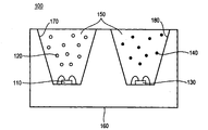
- FIG. 1 is a vertical cross-sectional view of a white LED device according to a preferred embodiment of the present invention
- FIGS. 2 and 3 are vertical cross-sectional view showing a laminated structure of the LED chip of the white LED device according to a preferred embodiment of the present invention
- FIG. 4 is a vertical sectional view of a white LED device according to another preferred embodiment of the present invention.
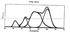
- FIG. 5 is a graph showing a white light spectrum of a white LED device according to a preferred embodiment of the present invention.
- FIG. 6 is a graph showing a white light spectrum of a white LED device according to another preferred embodiment of the present invention.
- a white LED device has a technical feature of implementing white light close to natural light by combining an LED chip having a peak wavelength of 440 to 560 nm and a phosphor having a peak wavelength of 560 to 670 nm. Specific embodiments of the present invention will be described in detail with reference to the accompanying drawings.
- FIG. 1 is a vertical sectional view of a white LED device according to a preferred embodiment of the present invention.
- a white LED device 100 includes a blue LED chip 110, a yellow phosphor 120, a green LED chip 130, and a red phosphor 140. It may be configured to include.
- the blue LED chip 110 emits blue light at a peak wavelength in the wavelength range of 440 ⁇ 490nm, and the yellow phosphor 120 absorbs a part of the blue light emitted from the blue LED chip 110 to be excited Yellow light is emitted at the peak wavelength of 560 ⁇ 615nm.
- the green LED chip 130 emits green light at a peak wavelength in a wavelength range of 500 to 560 nm
- the red phosphor 140 absorbs a part of the green light emitted from the green LED chip 130 and is excited. Red light is emitted at the peak wavelength of the 670 nm wavelength band.
- the blue and green light emitted from the blue LED chip 110 and the green LED chip 130, and the yellow phosphor 120 and the red excited by absorbing some of the blue light and green light Yellow light and red light emitted from the phosphor 140 are mixed to implement white light.
- the yellow phosphor 120 and the red phosphor 140 are processed in powder form so as to be excited by blue light and green light, respectively, and then uniformly mixed with the translucent resin 150 to allow the blue LED chip 110. And it is preferable that the green LED chip 130 is configured in a form surrounding the. Meanwhile, although the yellow phosphor 120 and the red phosphor 140 are illustrated in the form of powder, the form of the phosphor is not limited thereto, and may be variously modified to a pellet or a layered structure as necessary. It must be understood.
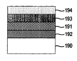
- 2 and 3 are vertical cross-sectional view showing the laminated structure of the LED chip of the white LED device according to a preferred embodiment of the present invention.
- the blue LED chip 110 and the green LED chip 130 may be manufactured using a nitride semiconductor such as AlInGaN.
- the nitride LED chip of the present invention is an active layer 191 for generating light as shown in Figure 2, and the n-type nitride layer formed on the lower portion of the active layer 191 to provide an electron (electron) 192 and a p-type nitride layer 193 stacked on top of the active layer 191 to provide a positron.
- reference numeral 190 denotes a substrate in FIGS. 2 and 3.
- the p-type ZnO layer 194 doped with As (arsenic) may be deposited on the p-type nitride layer 193 to form a thin film structure.
- the p-type ZnO layer 194 increases the light output by providing the active layer 191 with a positron that is relatively insufficient compared to the negative electron.
- green LED chips typically have an external quantum efficiency (EQE) of less than 30% and light output of less than 50% of a blue LED chip at the same injection current, which is known to have a very low light efficiency compared to a blue LED chip or a red LED chip. This is because the positron is not sufficiently supplied from the p-type nitride layer to the active layer.
- the process conditions are the same as those of the blue LED chip, the light output and the light efficiency can be increased, but the active layer, for example, Quantum Well, which generates green light due to the high deposition temperature It is destroyed and its effect cannot be achieved.
- the active layer for example, Quantum Well, which generates green light due to the high deposition temperature It is destroyed and its effect cannot be achieved.
- the light of the green LED chip 130 It is a stable improvement of output and light efficiency.
- the present invention if it has a sufficient positron concentration that can be provided to the active layer 191, and excellent transparency and high light transmittance, it is also possible to use a transparent oxide layer other than the p-type ZnO layer 194.
- a transparent oxide layer other than the p-type ZnO layer 194.
- a p-type BeZnO layer may be used as the transparent oxide layer, and such a configuration is preferable because the same effect as when using the p-type ZnO layer 194 may be obtained.
- indium tin oxide (ITO) having good transparency or metal (Metal) having good reflectivity may be deposited on the transparent oxide layer to form a good ohmic contact.
- the yellow phosphor 120 may include a YAG series containing a rare earth element such as Ce-doped ((YGd) 5 Al 5 O 3 ), or a silicate-based phosphor such as Eu-doped Sr 3 SiO 5 . Can be used.
- a rare earth element such as Ce-doped ((YGd) 5 Al 5 O 3 )
- a silicate-based phosphor such as Eu-doped Sr 3 SiO 5 .
- the red phosphor 140 may be selected from among a nitride series containing rare earth elements such as Eu-doped SrBaCaAlSiN 3 , an oxide series such as Eu-doped Y 2 O 3 , or a sulfide series such as Eu-doped CaS. have.
- the nitride series includes LxMyN ((2/3) x + (4/3) y): R or LxMyOzN ((2/3) x + (4/3) y- (2/3) z): R (
- R Y, La, Ce, Pr, Nd, Sm, Eu, Gd, Tb, Dy, Ho, Er, Lu, at least one or more selected from rare earth elements essential for Eu
- 6MgO) As 2 O 5 ): Mn
- (3.5MgO) 0.5MgF 2 ) (GeO 2 ): Mn
- Li 2 TiO 3 Mn
- LiAlO 2 Mn
- MS Eu (wherein M: Mg, Ca, Sr, Ba, Zn, and at least one or more of Group II elements consisting of Cd) can be used.
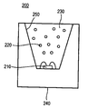
- FIG. 4 is a vertical sectional view of a white LED device according to another preferred embodiment of the present invention.
- the white LED device 200 may include a blue green LED chip 210 and a red phosphor 220.
- the bluish green LED chip 210 emits bluish green light at a peak wavelength of 490-550 nm, more preferably, 500-520 nm, and the red phosphor 220 emits light from the bluish green LED chip 210. After absorbing a part of the blue-green light and being excited, red light is emitted at a peak wavelength of 590 to 670 nm, more preferably 630 to 655 nm.
- the white LED device 200 when configured as described above and a current is applied through an electrode, blue green light is emitted from the blue green LED chip 210, and a part of the blue green light is absorbed by the red phosphor 220. do.
- the red phosphor 220 When a portion of the blue green light is absorbed as described above, the red phosphor 220 is excited to emit red light, and the red light and the unabsorbed blue green light emitted from the blue green LED chip 210 are mixed to emit white light.
- the red phosphor 220 is processed in a powder form so as to be excited by the blue green light, and then uniformly mixed with the translucent resin 230 is configured to surround the blue green LED chip 210.
- the red phosphor 220 may be mixed and used in a layered structure in the light transmitting resin 230 in the form of a thin mass, that is, a pellet, in addition to the powder form.
- the red phosphor 220 includes a nitride series containing rare earth elements (eg, Eu-doped SrBaCaAlSiN 3 ), an oxide series (eg, Eu-doped Y 2 O 3 ), or a sulfide series (eg, Eu-doped CaS). ) Can be used to choose an enemy.
- a nitride series containing rare earth elements eg, Eu-doped SrBaCaAlSiN 3
- an oxide series eg, Eu-doped Y 2 O 3
- a sulfide series eg, Eu-doped CaS
- the blue green LED chip 210 may be manufactured using a nitride semiconductor of AlInGaN, and more specifically, an active layer 191 for generating light and electrons in the active layer 191 as described with reference to FIG. 2.
- the n-type nitride layer 192 may be provided and the p-type nitride layer 193 may be configured to provide a positron to the active layer 191.
- a p-type ZnO layer 194 doped with As (arsenic) is deposited on the p-type nitride layer 193 to form a thin film structure, as described above.
- a positron may be additionally provided in the active layer 191 to improve light output.
- the white LED device according to another exemplary embodiment of the present invention has been described above. Hereinafter will be described the specific installation method of the present invention.
- the blue green LED chip 210 and the red phosphor 220 may be installed in the package body 240.
- the concave reflection cup 250 is formed inside the package body 240, the blue green LED chip 210 is mounted on the bottom surface of the reflection cup 250, and the red phosphor 220 is
- the transparent cup 230 is accommodated in the reflective cup 250 in a form of surrounding the bluish green LED chip 210.
- FIG. 4 for convenience of description, an electrode pattern or a lead frame electrically connected to the LED chip is not illustrated.
- FIG. 4 for convenience of description, an electrode pattern or a lead frame electrically connected to the LED chip is not illustrated.
- FIG. 4 for convenience of description, an installation method may be equally applied to the embodiment of FIG. 1.
- the blue green LED chip 210 and the red phosphor 220 may be directly mounted on a PCB substrate (not shown) using COB (Chip On Board) technology.
- the red phosphor 220 is applied together with the translucent resin on the bluish green LED chip 210 using a mold.
- the white light spectrum was measured by adjusting the emission peak wavelength of the LED chip and the phosphor, and the results are shown in FIG. 5. .
- a blue LED chip having a peak wavelength of 450 to 475 nm, a green LED chip having a peak wavelength of 525 to 535 nm, a yellow phosphor having a peak wavelength of 560 to 580 nm, and a peak wavelength of 625 to 660 nm When the red phosphor was used, white light having excellent color rendering properties was obtained.
- the correlation color temperature and the color rendering index of the white light emitted in the above-described peak wavelength range were measured, and the results are shown in Table 1 below compared with the case of a white LED manufactured using a conventional general YAG-based phosphor.
- the correlation color temperature was measured by using a known color temperature measuring instrument, and the color rendering index was determined by measuring the spectrum of white light and comparing the distribution of the emission spectrum of the standard light source.
- the external quantum efficiency and light output of the green LED chip are compared with the conventional green LED in Table 2 below.
- the present invention improves energy efficiency by minimizing non-luminescent light output loss generated when the phosphor is excited. It is expected to be possible.
- the white light spectrum was measured by adjusting the emission peak wavelength of the LED chip and the phosphor, and the results are shown in FIG. 6.
- white light having excellent color rendering was obtained when a blue green LED chip having a peak wavelength of 500 to 520 nm and a red phosphor having a peak wavelength of 590 to 670 nm were used.
Abstract
La présente invention concerne un appareil à LED blanche comprenant une puce LED bleue émettant une lumière bleue dans une bande de longueur d'onde de 440 nm à 490 nm, un corps fluorescent jaune formé sur la puce LED bleue et excité par la lumière bleue pour émettre une lumière jaune dans une bande de longueur d'onde de 560 nm à 615 nm, une puce LED verte émettant une lumière verte dans une bande de longueur d'onde de 500 nm à 560 nm et un corps fluorescent rouge formé sur la puce LED verte et excité par la lumière verte pour émettre une lumière rouge dans une bande de longueur d'onde de 615 nm à 670 nm, ou comprenant une puce LED vert bleuté émettant une lumière vert bleuté dans une bande de longueur d'onde de 490 nm à 550 nm, et un corps fluorescent rouge formé sur la puce LED vert bleuté et excité par la lumière vert bleuté pour émettre une lumière rouge dans une bande de longueur d'onde de 590 nm à 670 nm, cet appareil produisant une lumière blanche présentant un indice de rendu des couleurs élevé et une faible température de couleur proximale.
Priority Applications (1)
| Application Number | Priority Date | Filing Date | Title |
|---|---|---|---|
| US14/235,473 US20140209944A1 (en) | 2011-07-28 | 2012-07-24 | White led apparatus |
Applications Claiming Priority (4)
| Application Number | Priority Date | Filing Date | Title |
|---|---|---|---|
| KR20110074859 | 2011-07-28 | ||
| KR10-2011-0074859 | 2011-07-28 | ||
| KR1020120036210A KR101395432B1 (ko) | 2011-07-28 | 2012-04-06 | 백색 led 장치 |
| KR10-2012-0036210 | 2012-04-06 |
Publications (2)
| Publication Number | Publication Date |
|---|---|
| WO2013015597A2 true WO2013015597A2 (fr) | 2013-01-31 |
| WO2013015597A3 WO2013015597A3 (fr) | 2013-03-21 |
Family
ID=47601643
Family Applications (1)
| Application Number | Title | Priority Date | Filing Date |
|---|---|---|---|
| PCT/KR2012/005889 WO2013015597A2 (fr) | 2011-07-28 | 2012-07-24 | Appareil à led blanche |
Country Status (1)
| Country | Link |
|---|---|
| WO (1) | WO2013015597A2 (fr) |
Cited By (8)
| Publication number | Priority date | Publication date | Assignee | Title |
|---|---|---|---|---|
| US20140313234A1 (en) * | 2013-04-18 | 2014-10-23 | Hon Hai Precision Industry Co., Ltd. | Brightness control device and method |
| WO2016114598A1 (fr) * | 2015-01-15 | 2016-07-21 | 주식회사 엘엠에스 | Dispositif d'affichage |
| CN108843984A (zh) * | 2018-06-27 | 2018-11-20 | 朗昭创新控股(深圳)有限公司 | 一种全自然光谱led发光体及照明装置 |
| CN109000160A (zh) * | 2018-06-27 | 2018-12-14 | 朗昭创新控股(深圳)有限公司 | 一种准自然光led光源及照明装置 |
| WO2019050260A1 (fr) * | 2017-09-06 | 2019-03-14 | 지엘비텍 주식회사 | Module d'éclairage à del standard d50/d65 à rendu de couleur élevée et appareil d'éclairage |
| CN111795307A (zh) * | 2020-07-02 | 2020-10-20 | 中国计量大学 | 一种实现低蓝光危害、高显色的led装置 |
| US10982824B2 (en) | 2017-09-06 | 2021-04-20 | Glbtech Co., Ltd. | High color rendering D50/D65 standard LED illuminant module and lighting apparatus |
| CN113497012A (zh) * | 2020-03-20 | 2021-10-12 | 海迪科(南通)光电科技有限公司 | 一种类太阳光谱封装结构及其制备方法 |
Citations (4)
| Publication number | Priority date | Publication date | Assignee | Title |
|---|---|---|---|---|
| JP2007080880A (ja) * | 2005-09-09 | 2007-03-29 | Matsushita Electric Works Ltd | 発光装置 |
| US7227196B2 (en) * | 2003-05-20 | 2007-06-05 | Burgener Ii Robert H | Group II-VI semiconductor devices |
| KR20100012849A (ko) * | 2009-09-14 | 2010-02-08 | 서울반도체 주식회사 | 웜화이트 발광장치 및 그것을 포함하는 백라이트 모듈 |
| JP2010258479A (ja) * | 2010-08-16 | 2010-11-11 | Citizen Electronics Co Ltd | 発光装置 |
-
2012
- 2012-07-24 WO PCT/KR2012/005889 patent/WO2013015597A2/fr active Application Filing
Patent Citations (4)
| Publication number | Priority date | Publication date | Assignee | Title |
|---|---|---|---|---|
| US7227196B2 (en) * | 2003-05-20 | 2007-06-05 | Burgener Ii Robert H | Group II-VI semiconductor devices |
| JP2007080880A (ja) * | 2005-09-09 | 2007-03-29 | Matsushita Electric Works Ltd | 発光装置 |
| KR20100012849A (ko) * | 2009-09-14 | 2010-02-08 | 서울반도체 주식회사 | 웜화이트 발광장치 및 그것을 포함하는 백라이트 모듈 |
| JP2010258479A (ja) * | 2010-08-16 | 2010-11-11 | Citizen Electronics Co Ltd | 発光装置 |
Cited By (10)
| Publication number | Priority date | Publication date | Assignee | Title |
|---|---|---|---|---|
| US20140313234A1 (en) * | 2013-04-18 | 2014-10-23 | Hon Hai Precision Industry Co., Ltd. | Brightness control device and method |
| WO2016114598A1 (fr) * | 2015-01-15 | 2016-07-21 | 주식회사 엘엠에스 | Dispositif d'affichage |
| WO2019050260A1 (fr) * | 2017-09-06 | 2019-03-14 | 지엘비텍 주식회사 | Module d'éclairage à del standard d50/d65 à rendu de couleur élevée et appareil d'éclairage |
| US10982824B2 (en) | 2017-09-06 | 2021-04-20 | Glbtech Co., Ltd. | High color rendering D50/D65 standard LED illuminant module and lighting apparatus |
| CN108843984A (zh) * | 2018-06-27 | 2018-11-20 | 朗昭创新控股(深圳)有限公司 | 一种全自然光谱led发光体及照明装置 |
| CN109000160A (zh) * | 2018-06-27 | 2018-12-14 | 朗昭创新控股(深圳)有限公司 | 一种准自然光led光源及照明装置 |
| CN113497012A (zh) * | 2020-03-20 | 2021-10-12 | 海迪科(南通)光电科技有限公司 | 一种类太阳光谱封装结构及其制备方法 |
| CN113497012B (zh) * | 2020-03-20 | 2024-02-23 | 海迪科(南通)光电科技有限公司 | 一种类太阳光谱封装结构及其制备方法 |
| CN111795307A (zh) * | 2020-07-02 | 2020-10-20 | 中国计量大学 | 一种实现低蓝光危害、高显色的led装置 |
| CN111795307B (zh) * | 2020-07-02 | 2023-06-27 | 中国计量大学 | 一种实现低蓝光危害、高显色的led装置 |
Also Published As
| Publication number | Publication date |
|---|---|
| WO2013015597A3 (fr) | 2013-03-21 |
Similar Documents
| Publication | Publication Date | Title |
|---|---|---|
| KR101395432B1 (ko) | 백색 led 장치 | |
| WO2013015597A2 (fr) | Appareil à led blanche | |
| US8779455B2 (en) | Semiconductor light-emitting device, semiconductor light-emitting system and illumination fixture | |
| TWI289229B (en) | Light emitting device, and back light and liquid crystal display employing it | |
| KR100609830B1 (ko) | 녹색 및 적색형광체를 이용하는 백색 반도체 발광장치 | |
| KR100666265B1 (ko) | 형광체 및 이를 이용한 발광소자 | |
| CN101252159B (zh) | 白色发光器件 | |
| JP2023058559A (ja) | フルスペクトル白色発光デバイス | |
| WO2012077448A1 (fr) | Dispositif d'émission de lumière | |
| JP2008034188A (ja) | 照明装置 | |
| US8044410B2 (en) | White light-emitting diode and its light conversion layer | |
| JP2006527501A (ja) | 発光素子及び発光素子の蛍光体 | |
| US7834372B2 (en) | High luminous flux warm white solid state lighting device | |
| TW201010125A (en) | White light light-emitting diodes | |
| TW201143160A (en) | Light-emitting device | |
| JP2008235458A (ja) | 白色発光装置、これを用いてなるバックライトおよび表示装置並びに照明装置 | |
| CN201209828Y (zh) | 宽谱白光led | |
| US7026656B2 (en) | White light-emitting device | |
| KR100605212B1 (ko) | 형광체 및 이를 이용한 백색 발광다이오드 | |
| US7701124B2 (en) | White light-emitting device having a cap layer formed from a mixture of silicon and a phosphor blend | |
| TW572994B (en) | Method for manufacturing white light source | |
| KR100707871B1 (ko) | 조명용 백색 발광장치 | |
| KR20040088446A (ko) | 백색 발광소자 | |
| CN1919854A (zh) | 化合物、包含它的荧光粉组合物及发光装置 | |
| KR100647823B1 (ko) | 조명용 백색 발광장치 |
Legal Events
| Date | Code | Title | Description |
|---|---|---|---|
| 121 | Ep: the epo has been informed by wipo that ep was designated in this application |
Ref document number: 12818202 Country of ref document: EP Kind code of ref document: A2 |
|
| NENP | Non-entry into the national phase |
Ref country code: DE |
|
| WWE | Wipo information: entry into national phase |
Ref document number: 14235473 Country of ref document: US |
|
| 122 | Ep: pct application non-entry in european phase |
Ref document number: 12818202 Country of ref document: EP Kind code of ref document: A2 |