WO2013011845A1 - 実装基板用放熱積層材の製造方法 - Google Patents
実装基板用放熱積層材の製造方法 Download PDFInfo
- Publication number
- WO2013011845A1 WO2013011845A1 PCT/JP2012/067263 JP2012067263W WO2013011845A1 WO 2013011845 A1 WO2013011845 A1 WO 2013011845A1 JP 2012067263 W JP2012067263 W JP 2012067263W WO 2013011845 A1 WO2013011845 A1 WO 2013011845A1
- Authority
- WO
- WIPO (PCT)
- Prior art keywords
- mass
- less
- heat
- aluminum foil
- thickness
- Prior art date
- Legal status (The legal status is an assumption and is not a legal conclusion. Google has not performed a legal analysis and makes no representation as to the accuracy of the status listed.)
- Ceased
Links
Images



Classifications
-
- H—ELECTRICITY
- H05—ELECTRIC TECHNIQUES NOT OTHERWISE PROVIDED FOR
- H05K—PRINTED CIRCUITS; CASINGS OR CONSTRUCTIONAL DETAILS OF ELECTRIC APPARATUS; MANUFACTURE OF ASSEMBLAGES OF ELECTRICAL COMPONENTS
- H05K1/00—Printed circuits
- H05K1/02—Details
- H05K1/03—Use of materials for the substrate
- H05K1/05—Insulated conductive substrates, e.g. insulated metal substrate
-
- H—ELECTRICITY
- H05—ELECTRIC TECHNIQUES NOT OTHERWISE PROVIDED FOR
- H05K—PRINTED CIRCUITS; CASINGS OR CONSTRUCTIONAL DETAILS OF ELECTRIC APPARATUS; MANUFACTURE OF ASSEMBLAGES OF ELECTRICAL COMPONENTS
- H05K3/00—Apparatus or processes for manufacturing printed circuits
- H05K3/0058—Laminating printed circuit boards onto other substrates, e.g. metallic substrates
- H05K3/0061—Laminating printed circuit boards onto other substrates, e.g. metallic substrates onto a metallic substrate, e.g. a heat sink
-
- H—ELECTRICITY
- H05—ELECTRIC TECHNIQUES NOT OTHERWISE PROVIDED FOR
- H05K—PRINTED CIRCUITS; CASINGS OR CONSTRUCTIONAL DETAILS OF ELECTRIC APPARATUS; MANUFACTURE OF ASSEMBLAGES OF ELECTRICAL COMPONENTS
- H05K7/00—Constructional details common to different types of electric apparatus
- H05K7/20—Modifications to facilitate cooling, ventilating, or heating
-
- H—ELECTRICITY
- H05—ELECTRIC TECHNIQUES NOT OTHERWISE PROVIDED FOR
- H05K—PRINTED CIRCUITS; CASINGS OR CONSTRUCTIONAL DETAILS OF ELECTRIC APPARATUS; MANUFACTURE OF ASSEMBLAGES OF ELECTRICAL COMPONENTS
- H05K1/00—Printed circuits
- H05K1/02—Details
- H05K1/0201—Thermal arrangements, e.g. for cooling, heating or preventing overheating
- H05K1/0203—Cooling of mounted components
Definitions
- the present invention generally relates to a method for manufacturing a heat dissipation laminate for a mounting substrate, and more specifically, a method for manufacturing a heat dissipation laminate for a mounting substrate for mounting an electronic element having a large amount of heat generation, for example, a light emitting diode.
- the present invention relates to a method for manufacturing a heat dissipating laminated material for a mounting substrate for mounting a light emitting element such as (LED).
- the circuit is formed of copper, aluminum foil, or paste composition.
- An electronic element is mounted on the formed circuit. Examples of the mounted electronic element include a resistor element, a capacitor, a transistor, various power elements; a high-density integrated circuit such as an MPU or a CPU; a light-emitting element such as a light-emitting diode (LED) or a laser diode; and an array element thereof.
- a mounting substrate for mounting an electronic element can be directly laminated on a support or casing of a portable electronic device, it is effective for thinning. That is, the mounting substrate is required to be flexible.
- LEDs have been used as light sources for liquid crystal backlight devices.
- the LED is directly mounted on an insulating substrate.
- the side-edge type liquid crystal backlight device has a structure in which a large number of LEDs are mounted per unit area, and therefore, a higher heat dissipation is required for the mounting substrate laminate.
- Patent Document 1 heat generated from an electronic component such as an LED is efficiently released, and is thin and light, and has a desired three-dimensional structure by plastic working.
- a metal substrate that can be formed a substrate in which a copper-based layer formed on one surface of a stainless steel foil is bonded to a copper foil for circuit formation with an insulating layer interposed is disclosed.
- a method of selectively etching a copper foil is generally employed as a method for forming a circuit on the mounting surface of a metal substrate as described above.
- the copper foil is selectively etched after the copper foil is bonded to the metal foil (stainless steel foil in Patent Document 1).
- an object of the present invention is to cope with the reduction in weight, size and thickness of electronic devices, and more efficiently generates heat generated by electronic devices even when electronic devices with large heat generation are mounted. It is providing the manufacturing method of the thermal radiation laminated material for mounting substrates which can be disperse
- the manufacturing method of the heat dissipation laminated material for a mounting substrate according to the present invention includes the following steps.
- the aluminum foil contains 0.5 mass% to 3.0 mass% manganese, 0.0001 mass% to less than 0.2 mass% chromium, and magnesium. 0.2% by mass or more and 1.8% by mass or less, titanium by 0.0001% by mass or more and 0.6% by mass or less, copper by more than 0% by mass and 0.005% by mass or less, and silicon by more than 0% by mass 0 0.1% by mass or less, including iron exceeding 0% by mass and 0.2% by mass or less, with the balance being aluminum and inevitable impurities.
- the insulating film preferably contains one selected from the group consisting of polyimide, polyethylene naphthalate, polyethylene terephthalate, and polytetrafluoroethylene.
- the heat-dissipating laminated material for mounting substrates manufactured according to the present invention has an aluminum foil with excellent lightness, heat dissipation (thermal conductivity) and flexibility, so that it can respond to weight reduction, size reduction and thickness reduction of electronic devices. can do.
- the aluminum foil having a predetermined strength and hardness is fixed to the surface opposite to the one surface of the insulating film. There are no irregularities on the surface.
- the heat-dissipating laminated material for a mounting substrate manufactured in the present invention is used by being attached to a support or casing of a portable electronic device, voids are not generated and the thermal conductivity is not lowered. . Therefore, even when an electronic element having a large calorific value is mounted, it is possible to manufacture a mounting board heat dissipating laminated material that can dissipate the heat generated in the electronic element more efficiently.
- a copper layer 20 which is an example of a conductive layer, is fixed to a surface of one side of a resin film 10, which is an example of an insulating film, with an adhesive layer (not shown) interposed therebetween.
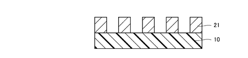
- the circuit pattern layer 21 is formed by selectively etching the copper layer 20 as shown in FIG.
- the aluminum foil 30 is fixed to the surface of the resin film 10 opposite to the surface on one side with an adhesive layer (not shown) interposed therebetween.
- the aluminum foil 30 is 0.5 mass% or more and 3.0 mass% or less of manganese, 0.0001 mass% or more and less than 0.2 mass% of chromium, and 0.2 mass% or more and 1.8 mass% of magnesium. % Or less, titanium 0.0001 mass% or more and 0.6 mass% or less, copper over 0 mass% to 0.005 mass% or less, silicon over 0 mass% to 0.1 mass% or less, iron 0 mass % And 0.2% by mass or less, with the balance being aluminum and inevitable impurities.
- This aluminum foil 30 exhibits high strength and high hardness by having the above composition, for example, a hardness of 170 Hv.
- the mounting board heat dissipation laminate of the present invention manufactured as described above includes the aluminum foil 30 that is excellent in lightness, heat dissipation (thermal conductivity), and flexibility. It can cope with downsizing and thinning.
- the aluminum foil 30 having a predetermined strength and hardness is fixed to the surface opposite to the one surface of the resin film 10 after the circuit pattern layer 21 is formed, the surface of the aluminum foil 30 is uneven. Does not occur.
- the heat-dissipating laminated material for a mounting substrate manufactured in the present invention is used by being attached to a support or casing of a portable electronic device, voids are not generated and the thermal conductivity is not lowered. . Therefore, even when an electronic element having a large calorific value is mounted, it is possible to manufacture a mounting board heat dissipating laminated material that can dissipate the heat generated in the electronic element more efficiently.
- the resin film 10 has a glass transition temperature (Tg) of 250 ° C. or higher so that it can withstand mounting of an electronic element by solder at about 250 ° C.
- Tg glass transition temperature
- the resin film 10 preferably has a dielectric breakdown voltage of 5 kV or more in order to ensure insulation.
- the resin film 10 has almost no heat shrinkage, that is, the heat shrinkage rate is 0.1% or less.
- the resin film 10 is preferably formed from a film containing polyimide, polyethylene naphthalate or polyethylene terephthalate, and a polyimide film is particularly preferably used as the material of the resin film 10.
- the thickness of the resin film 10 is preferably 10 ⁇ m or more and 100 ⁇ m or less, more preferably 10 to 50 ⁇ m, in order to exhibit stable insulation and heat dissipation. If the thickness of the resin film 10 is less than 10 ⁇ m, a stable insulating effect cannot be obtained. When the thickness of the resin film 10 exceeds 100 ⁇ m, it causes a decrease in heat dissipation.
- the copper layer 20 is provided in order to form a circuit for wiring an electronic element mounted on the mounting board heat dissipation laminate by etching or the like. Although it may be configured by depositing a copper film as the copper layer 20 on the polyimide resin layer as the resin film 10, electrolytic copper as the copper layer 20 with an adhesive layer interposed on the resin film 10. It is preferable to be constituted by laminating foils.
- the thickness of the copper layer 20 is preferably 5 ⁇ m or more and 100 ⁇ m or less, more preferably 10 to 70 ⁇ m, so that a circuit can be easily formed by etching and laminated on the resin film 10 in close contact.
- the thickness of the copper layer 20 is less than 5 ⁇ m, it becomes difficult to adhere and laminate the resin layer 10 neatly (so as not to cause wrinkles or the like). If the thickness of the copper layer 20 exceeds 100 ⁇ m, precise circuit formation by etching becomes difficult.
- the aluminum foil 30 is provided in order to dissipate heat generated from the electronic elements mounted on the circuit pattern layer 21 of the mounting board heat dissipation laminate.
- the heat dissipating laminated material for the mounting substrate is arranged so that the lower surface of the aluminum foil 30 (the surface opposite to the surface fixed to the resin film 10) is laminated and fixed along the support or casing of the electronic device. May be.
- the aluminum foil 30 is preferably formed from an aluminum material having high thermal conductivity. When laminating the heat-dissipating laminated material for the mounting substrate along the support or casing of the electronic device, a material having good flexibility is required. Therefore, the aluminum foil 30 should be appropriately conditioned aluminum material. preferable.
- the thickness of the aluminum foil 30 is preferably 20 ⁇ m or more and 350 ⁇ m or less, more preferably 80 ⁇ m or more, in order to contribute to the lightness, miniaturization, and thinning of the electronic device, facilitate processing, and exhibit stable heat dissipation. It is 300 ⁇ m or less, more preferably 100 ⁇ m or more and 250 ⁇ m or less.
- the thickness of the aluminum foil 30 is less than 20 ⁇ m, a stable heat dissipation effect cannot be obtained.
- the thickness of the aluminum foil 30 exceeds 350 ⁇ m, it becomes difficult to process, and it becomes an obstacle to reduction in weight, size, and thickness.
- the adhesive layer is preferably formed from a general-purpose epoxy adhesive in order to ensure heat resistance. Although the conductive filler increases the heat dissipation, it lowers the insulating properties, so that the conductive filler is not included in the adhesive layer.
- the thickness of the adhesive layer is preferably 3 ⁇ m or more and 30 ⁇ m or less in order to exhibit good adhesion and not to prevent heat dissipation. If the thickness of the adhesive layer is less than 3 ⁇ m, insufficient adhesion or uneven adhesion tends to occur, which causes a decrease in heat dissipation. When the thickness of the adhesive layer exceeds 30 ⁇ m, it becomes difficult to laminate the aluminum foil 30 and the resin film 10, and the resin film 10 and the copper layer 20, which causes a decrease in heat dissipation.
- Example shown below is an example and this invention is not limited to the following Example.
- a sample of an example of a heat dissipating laminated material for a mounting substrate was prepared according to the steps shown in FIGS. Further, for comparison, a sample of Comparative Example 1 of the heat dissipating laminated material for mounting substrate was manufactured according to the steps shown in FIGS. 1 to 3 using an aluminum foil having a hardness lower than that of the aluminum foil used in the present invention. Further, according to the steps shown in FIGS. 4 to 5, a sample of Comparative Example 2 of the heat dissipating laminated material for mounting substrate was produced.
- Example 2 As shown in FIG. 1, a polyimide film having a thickness of 25 ⁇ m is used as the resin film 10, and an epoxy-based adhesive is interposed on one side of the film, and an electrolytic copper foil having a thickness of 35 ⁇ m is dried as the copper layer 20. Bonded by the lamination method. The thickness of the adhesive layer was 15 ⁇ m.
- a circuit pattern layer 21 having an arbitrary circuit shape was formed by selectively etching the copper layer 20 using a photolithography method.
- an epoxy adhesive is interposed on the other surface of the resin film 10, and manganese is 0.5 mass% or more and 3.0 mass% or less, and chromium is 0.0001 mass. % To less than 0.2% by weight, magnesium from 0.2% to 1.8% by weight, titanium from 0.0001% to 0.6% by weight, copper from 0% to over 0.005% %, Less than 0.1% by weight of silicon, more than 0% by weight and less than 0.2% by weight of iron, the balance being aluminum and unavoidable impurities, and an aluminum foil with a thickness of 100 ⁇ m 30 (hardness 170 Hv) was bonded by a dry lamination method. The thickness of the adhesive layer was 15 ⁇ m.
- Comparative Example 1 to 3 are the same as in the example except that an aluminum foil having a thickness of 150 ⁇ m (material 1N30, H, hardness: 50 Hv) is used instead of the aluminum foil 30 having a thickness of 100 ⁇ m used in the example. According to the process, a heat dissipating laminated material for a mounting substrate was produced.
- a polyimide film having a thickness of 25 ⁇ m is used as the resin film 10, and an epoxy-based adhesive is interposed on one side of the film, and an electrolytic copper foil having a thickness of 35 ⁇ m is dried as the copper layer 20. Bonded by the lamination method.
- the thickness of the adhesive layer was 15 ⁇ m.
- an aluminum foil (material: 1N30, H, hardness: 50 Hv) having a thickness of 150 ⁇ m was adhered to the other surface of the resin film 10 by a dry lamination method with an epoxy adhesive interposed therebetween.
- the copper layer 20 was selectively etched to form a circuit pattern layer 21 having an arbitrary circuit shape as in the example.
- the evaluation of the unevenness is visually observed from the side of the aluminum foil 30, and a part of the contour of the circuit pattern formed on the circuit pattern layer 21 is raised in an embossed shape, and the contour of the circuit pattern is not raised. A flat one was evaluated as having no unevenness. In the example, unevenness did not occur on the surface of the aluminum foil 30, whereas in Comparative Examples 1 and 2, unevenness occurred on the surface of the aluminum foil 30.
Landscapes
- Engineering & Computer Science (AREA)
- Microelectronics & Electronic Packaging (AREA)
- Manufacturing & Machinery (AREA)
- Physics & Mathematics (AREA)
- Thermal Sciences (AREA)
- Insulated Metal Substrates For Printed Circuits (AREA)
- Laminated Bodies (AREA)
Abstract
電子機器の軽量化と小型化と薄型化に対応することができるとともに、発熱量の大きい電子素子を実装しても、その電子素子で発生した熱をより効率的に放散することが可能な実装基板用放熱積層材の製造方法を提供する。樹脂フィルム(10)の一方側の表面に銅層(20)を固着させ、銅層(20)を選択的にエッチングすることにより回路パターン層(21)を形成し、回路パターン層(21)を形成した後に、樹脂フィルム(10)の一方側の表面とは反対側の表面にアルミニウム箔(30)を固着させる。
Description
本発明は、一般的には、実装基板用放熱積層材の製造方法に関し、特定的には、発熱量の大きい電子素子を実装するための実装基板用放熱積層材の製造方法、たとえば、発光ダイオード(LED)等の発光素子を実装するための実装基板用放熱積層材の製造方法に関するものである。
絶縁層の片面または両面に回路を形成した実装基板が幅広い分野に利用されている。回路は銅、アルミニウムの箔、または、ペースト組成物で形成される。形成された回路の上に電子素子が実装される。実装される電子素子としては、抵抗素子、コンデンサ、トランジスタ、各種パワー素子;MPU、CPU等の高密度集積回路;発光ダイオード(LED)、レーザーダイオード等の発光素子およびこれらのアレイ素子が挙げられる。
近年、電子機器に要求される性能はますます高くなり、上記の電子素子の中でもパワー素子や高密度集積回路の消費電力は増大する傾向にある。また、発光素子はさらに高輝度のものが開発されている。しかしながら、パワー素子や高密度集積回路の消費電力の増加や発光素子の輝度の向上による発熱量の増大は、発熱する電子素子自身や他の電子素子に悪影響を与える。たとえば、発熱する電子素子自身や他の電子素子が、熱によって誤作動すること、熱によって性能が低下すること、熱によって寿命が短縮すること等が考えられる。したがって、電子素子で発生した熱を効率よく取り除き、放散するための構造が種々提案されている。
一方、近年、携帯電話、デジタルカメラ、オーディオプレイヤー、ボイスレコーダー、ゲーム機等の携帯型電子機器では、軽量化と小型化に加えて薄型化が要求されている。電子素子を実装するための実装基板を携帯型電子機器の支持体や筐体に直接積層することができれば薄型化に効果的である。すなわち、実装基板に屈曲性が求められている。
また、液晶テレビなどの薄型テレビは、近年ますます大型化する傾向にある。しかしながら、薄型テレビでは、画面を大型化するとともに、テレビ本体を可能な限り軽量化および薄型化することが望まれている。薄型化や消費電力の低減のために、液晶バックライト装置の光源としてLEDを用いるようになってきている。LEDは絶縁基板に直接実装されるものである。このような技術的な傾向に対応するためには、LEDから発生した熱は、実装基板用積層材を介してLEDが実装される面とは反対側の面に放散する必要がある。特にサイドエッジ型の液晶バックライト装置は、その構造上、単位面積あたりに多数のLEDを実装するため、実装基板用積層材にはより高い放熱性が求められている。
そこで、たとえば、特開2010‐98246号公報(特許文献1)には、LED等の電子部品から発生する熱を効率よく放出し、薄型、軽量に優れ、かつ、塑性加工により所望の立体構造に形成可能な金属基板として、ステンレス箔の片面に形成した銅を主成分とする層が、絶縁層を介在させて、回路形成用の銅箔に接着されているものが開示されている。
ところで、上記のような金属基板の実装面に回路を形成する方法として、特許文献1に記載されているように、銅箔を選択的にエッチングする方法が一般的に採用される。この場合、金属箔(特許文献1ではステンレス箔)に銅箔を貼り合わせた後に銅箔が選択的にエッチングされる。
しかしながら、実装面側とは反対側の金属箔の強度が低く、厚みが薄い場合、実装面に形成された回路の凹凸が実装面側とは反対側の金属箔側に押し込まれ、金属箔の表面に転写されて凹凸が浮き出て平滑性が低下する。さらに、凹凸が付いた金属箔の面を携帯型電子機器の支持体や筐体に貼り付けて使用すると、空隙が生じて熱伝導率を低下させてしまうという問題がある。
そこで、本発明の目的は、電子機器の軽量化と小型化と薄型化に対応することができるとともに、発熱量の大きい電子素子を実装しても、その電子素子で発生した熱をより効率的に放散することが可能な実装基板用放熱積層材の製造方法を提供することである。
本発明に従った実装基板用放熱積層材の製造方法は、以下の工程を備える。
(A)絶縁性フィルムの一方側の表面に導電層を固着する工程
(B)導電層を選択的にエッチングすることにより、回路パターン層を形成する工程
(C)回路パターン層を形成した後に、絶縁性フィルムの一方側の表面とは反対側の表面にアルミニウム箔を固着する工程
本発明の実装基板用放熱積層材の製造方法において、アルミニウム箔が、マンガンを0.5質量%以上3.0質量%以下、クロムを0.0001質量%以上0.2質量%未満、マグネシウムを0.2質量%以上1.8質量%以下、チタンを0.0001質量%以上0.6質量%以下、銅を0質量%を超え0.005質量%以下、シリコンを0質量%を超え0.1質量%以下、鉄を0質量%を超え0.2質量%以下、含み、残部がアルミニウムと不可避的不純物とからなる。
また、本発明の実装基板用放熱積層材の製造方法において、絶縁性フィルムは、ポリイミド、ポリエチレンナフタレート、ポリエチレンテレフタレートおよびポリテトラフルオロエチレンからなる群より選ばれた1種を含むことが好ましい。
本発明によって製造された実装基板用放熱積層材が軽量性と放熱性(熱伝導性)と屈曲性に優れたアルミニウム箔を備えているので、電子機器の軽量化と小型化と薄型化に対応することができる。また、本発明によれば、回路パターン層を形成した後に、絶縁性フィルムの一方側の表面とは反対側の表面に、所定の強度と硬度を有するアルミニウム箔を固着するので、アルミニウム箔の表面に凹凸が生じない。これにより、本発明で製造された実装基板用放熱積層材を携帯型電子機器の支持体や筐体に貼り付けて使用しても、空隙が生じて熱伝導率を低下させてしまうことがない。したがって、発熱量の大きい電子素子を実装しても、その電子素子で発生した熱をより効率的に放散することが可能な実装基板用放熱積層材を製造することができる。
以下、本発明の一つの実施の形態を図面に基づいて説明する。
まず、図1に示すように、絶縁性フィルムの一例である樹脂フィルム10の一方側の表面に、接着剤層(図示せず)を介在させて、導電層の一例である銅層20を固着させる。
次に、銅層20を選択的にエッチングすることにより、図2に示すように、回路パターン層21を形成する。
そして、回路パターン層21を形成した後に、樹脂フィルム10の一方側の表面とは反対側の表面に、接着剤層(図示せず)を介在させて、アルミニウム箔30を固着させる。
ここで、アルミニウム箔30が、マンガンを0.5質量%以上3.0質量%以下、クロムを0.0001質量%以上0.2質量%未満、マグネシウムを0.2質量%以上1.8質量%以下、チタンを0.0001質量%以上0.6質量%以下、銅を0質量%を超え0.005質量%以下、シリコンを0質量%を超え0.1質量%以下、鉄を0質量%を超え0.2質量%以下、含み、残部がアルミニウムと不可避的不純物とからなる。このアルミニウム箔30は、上記の組成を有することにより、高い強度と高い硬度を示し、たとえば、170Hvの硬度を示す。
以上のようにして製造された本発明の実装基板用放熱積層材は、軽量性と放熱性(熱伝導性)と屈曲性に優れたアルミニウム箔30を備えているので、電子機器の軽量化と小型化と薄型化に対応することができる。また、回路パターン層21を形成した後に、樹脂フィルム10の一方側の表面とは反対側の表面に、所定の強度と硬度を有するアルミニウム箔30を固着するので、アルミニウム箔30の表面に凹凸が生じない。これにより、本発明で製造された実装基板用放熱積層材を携帯型電子機器の支持体や筐体に貼り付けて使用しても、空隙が生じて熱伝導率を低下させてしまうことがない。したがって、発熱量の大きい電子素子を実装しても、その電子素子で発生した熱をより効率的に放散することが可能な実装基板用放熱積層材を製造することができる。
(樹脂フィルム)
樹脂フィルム10は、約250℃のはんだによる電子素子の実装に耐えられるようにガラス転移温度(Tg)が250℃以上であるのが好ましい。また、樹脂フィルム10は、絶縁性を担保するために絶縁破壊電圧が5kV以上であることが好ましい。さらに、樹脂フィルム10は、熱収縮がほぼないこと、すなわち、熱収縮率が0.1%以下であることが好ましい。
樹脂フィルム10は、約250℃のはんだによる電子素子の実装に耐えられるようにガラス転移温度(Tg)が250℃以上であるのが好ましい。また、樹脂フィルム10は、絶縁性を担保するために絶縁破壊電圧が5kV以上であることが好ましい。さらに、樹脂フィルム10は、熱収縮がほぼないこと、すなわち、熱収縮率が0.1%以下であることが好ましい。
樹脂フィルム10は、ポリイミド、ポリエチレンナフタレートやポリエチレンテレフタレートを含むフィルムから形成されるのが好ましく、樹脂フィルム10の材料としては特にポリイミドフィルムが好適に使用される。
樹脂フィルム10の厚みは、安定した絶縁性と放熱性を発揮するためには10μm以上100μm以下が好ましく、より好ましくは10~50μmである。樹脂フィルム10の厚みが10μm未満では、安定した絶縁性の効果を得ることができない。樹脂フィルム10の厚みが100μmを超えると、放熱性低下の原因となる。
(銅層)
銅層20は、実装基板用放熱積層材の上に実装される電子素子を配線するための回路をエッチング等により形成するために設けられる。樹脂フィルム10としてのポリイミド樹脂層の上に銅層20としての銅膜を蒸着することにより構成されてもよいが、樹脂フィルム10の上に接着剤層を介在して銅層20としての電解銅箔を積層することにより構成されるのが好ましい。
銅層20は、実装基板用放熱積層材の上に実装される電子素子を配線するための回路をエッチング等により形成するために設けられる。樹脂フィルム10としてのポリイミド樹脂層の上に銅層20としての銅膜を蒸着することにより構成されてもよいが、樹脂フィルム10の上に接着剤層を介在して銅層20としての電解銅箔を積層することにより構成されるのが好ましい。
銅層20の厚みは、エッチングにより容易に回路を形成し、樹脂フィルム10の上に密着するように積層するためには5μm以上100μm以下が好ましく、より好ましくは10~70μmである。銅層20の厚みが5μm未満では、きれいに(シワなどが生じないように)樹脂フィルム10の上に密着して積層することが困難になる。銅層20の厚みが100μmを超えると、エッチングによる精密な回路形成が困難になる。
(アルミニウム箔)
アルミニウム箔30は、実装基板用放熱積層材の回路パターン層21の上に実装される電子素子から発生する熱を放散するために設けられる。アルミニウム箔30の下面(樹脂フィルム10と固着される側の面とは反対側の面)を電子機器の支持体や筐体に沿って積層して固着するように実装基板用放熱積層材を配置してもよい。
アルミニウム箔30は、実装基板用放熱積層材の回路パターン層21の上に実装される電子素子から発生する熱を放散するために設けられる。アルミニウム箔30の下面(樹脂フィルム10と固着される側の面とは反対側の面)を電子機器の支持体や筐体に沿って積層して固着するように実装基板用放熱積層材を配置してもよい。
アルミニウム箔30は熱伝導率が高いアルミニウム材から形成されるのが好ましい。実装基板用放熱積層材を電子機器の支持体や筐体に沿って積層する際には、屈曲性が良好なものが求められるので、アルミニウム箔30は適宜調質されたアルミニウム材を用いるのが好ましい。
アルミニウム箔30の厚みは、電子機器の軽量性、小型化、薄型化に寄与するとともに、加工を容易にし、安定した放熱性を発揮するためには20μm以上350μm以下が好ましく、さらに好ましくは80μm以上300μm以下、より好ましくは100μm以上250μm以下である。アルミニウム箔30の厚みが20μm未満では、安定した放熱性の効果を得ることができない。アルミニウム箔30の厚みが350μmを超えると、加工が困難になる上、軽量・小型・薄型化の妨げとなる。
(接着剤層)
接着剤層は、耐熱性を担保するために汎用のエポキシ系接着剤から形成されるのが好ましい。導電性フィラーは放熱性を高めるが、絶縁性を低下させるので、接着剤層には導電性フィラーを含ませない。
接着剤層は、耐熱性を担保するために汎用のエポキシ系接着剤から形成されるのが好ましい。導電性フィラーは放熱性を高めるが、絶縁性を低下させるので、接着剤層には導電性フィラーを含ませない。
接着剤層の厚みは、良好な密着性を発揮し、放熱の妨げにならないようにするために3μ以上30μm以下であるのが好ましい。接着剤層の厚みが3μm未満では、密着不足や密着ムラが起こりやすいので、放熱性低下の原因となる。接着剤層の厚みが30μmを超えると、アルミニウム箔30と樹脂フィルム10、樹脂フィルム10と銅層20を積層し難くなるので、放熱性低下の原因となる。
次に、本発明の実施例を具体的に説明する。なお、以下に示す実施例は一例であり、本発明は下記の実施例に限定されるものではない。
図1~図3に示す工程に従って実装基板用放熱積層材の実施例の試料を作製した。また、比較のため、本発明で用いられるアルミニウム箔よりも低い硬度のアルミニウム箔を用いて図1~図3に示す工程に従って実装基板用放熱積層材の比較例1の試料を作製した。さらに、図4~図5に示す工程に従って実装基板用放熱積層材の比較例2の試料を作製した。
(実施例)
図1に示すように、樹脂フィルム10として厚みが25μmのポリイミドフィルムを用いて、このフィルムの片面に、エポキシ系接着剤を介在させて、銅層20として厚みが35μmの電解銅箔を、ドライラミネーション法により接着した。接着剤層の厚みは15μmであった。
図1に示すように、樹脂フィルム10として厚みが25μmのポリイミドフィルムを用いて、このフィルムの片面に、エポキシ系接着剤を介在させて、銅層20として厚みが35μmの電解銅箔を、ドライラミネーション法により接着した。接着剤層の厚みは15μmであった。
次に、図2に示すように、フォトリソグラフィー法を用いて、銅層20を選択的にエッチングすることにより、任意の回路形状を有する回路パターン層21を形成した。
そして、図3に示すように、樹脂フィルム10のもう一方側の面に、エポキシ系接着剤を介在させて、マンガンを0.5質量%以上3.0質量%以下、クロムを0.0001質量%以上0.2質量%未満、マグネシウムを0.2質量%以上1.8質量%以下、チタンを0.0001質量%以上0.6質量%以下、銅を0質量%を超え0.005質量%以下、シリコンを0質量%を超え0.1質量%以下、鉄を0質量%を超え0.2質量%以下、含み、残部がアルミニウムと不可避的不純物とからなり、厚みが100μmのアルミニウム箔30(硬度170Hv)を、ドライラミネーション法により接着した。接着剤層の厚みは15μmであった。
(比較例1)
実施例で用いた厚みが100μmのアルミニウム箔30の代わりに、厚みが150μmのアルミニウム箔(材質1N30、H、硬度:50Hv)を用いた以外は、実施例と同様に図1~図3に示す工程に従って、実装基板用放熱積層材を作製した。
実施例で用いた厚みが100μmのアルミニウム箔30の代わりに、厚みが150μmのアルミニウム箔(材質1N30、H、硬度:50Hv)を用いた以外は、実施例と同様に図1~図3に示す工程に従って、実装基板用放熱積層材を作製した。
(比較例2)
図4に示すように、樹脂フィルム10として厚みが25μmのポリイミドフィルムを用いて、このフィルムの片面に、エポキシ系接着剤を介在させて、銅層20として厚みが35μmの電解銅箔を、ドライラミネーション法により接着した。接着剤層の厚みは15μmであった。また、樹脂フィルム10のもう一方側の面に、エポキシ系接着剤を介在させて、厚みが150μmのアルミニウム箔(材質:1N30、H、硬度:50Hv)を、ドライラミネーション法により接着した。
図4に示すように、樹脂フィルム10として厚みが25μmのポリイミドフィルムを用いて、このフィルムの片面に、エポキシ系接着剤を介在させて、銅層20として厚みが35μmの電解銅箔を、ドライラミネーション法により接着した。接着剤層の厚みは15μmであった。また、樹脂フィルム10のもう一方側の面に、エポキシ系接着剤を介在させて、厚みが150μmのアルミニウム箔(材質:1N30、H、硬度:50Hv)を、ドライラミネーション法により接着した。
次に、図5に示すように、フォトリソグラフィー法を用いて、銅層20を選択的にエッチングすることにより、実施例と同様に任意の回路形状を有する回路パターン層21を形成した。
得られた実施例、比較例1および比較例2の実装基板用放熱積層材においてアルミニウム箔30の面の凹凸の有無を目視にて確認した。
凹凸の評価は、アルミニウム箔30の側から目視で観察し、回路パターン層21に形成した回路パターンの輪郭の一部がエンボス状に浮き出ているものを凹凸ありとし、回路パターンの輪郭が浮き出ずに平坦なものを凹凸なしと評価した。
実施例では凹凸がアルミニウム箔30の面に生じなかったのに対し、比較例1、2ではアルミニウム箔30の面に凹凸が生じた。
実施例では凹凸がアルミニウム箔30の面に生じなかったのに対し、比較例1、2ではアルミニウム箔30の面に凹凸が生じた。
今回開示された実施の形態と実施例はすべての点で例示であって制限的なものではないと考慮されるべきである。本発明の範囲は以上の実施の形態と実施例ではなく、請求の範囲によって示され、請求の範囲と均等の意味および範囲内でのすべての修正と変形を含むものであることが意図される。
本発明によれば、電子機器の軽量化と小型化と薄型化に対応することができるとともに、発熱量の大きい電子素子を実装しても、その電子素子で発生した熱をより効率的に放散することが可能な実装基板用放熱積層材を製造することができる。
10:樹脂フィルム、20:銅層、21:回路パターン層、30:アルミニウム箔。
Claims (2)
- 絶縁性フィルム(10)の一方側の表面に導電層(20)を固着する工程と、
前記導電層(20)を選択的にエッチングすることにより、回路パターン層(21)を形成する工程と、
前記回路パターン層(21)を形成した後に、前記絶縁性フィルム(10)の一方側の表面とは反対側の表面にアルミニウム箔(30)を固着する工程と、を備え、
前記アルミニウム箔(30)が、マンガンを0.5質量%以上3.0質量%以下、クロムを0.0001質量%以上0.2質量%未満、マグネシウムを0.2質量%以上1.8質量%以下、チタンを0.0001質量%以上0.6質量%以下、銅を0質量%を超え0.005質量%以下、シリコンを0質量%を超え0.1質量%以下、鉄を0質量%を超え0.2質量%以下、含み、残部がアルミニウムと不可避的不純物とからなる、実装基板用放熱積層材の製造方法。 - 前記絶縁性フィルム(10)は、ポリイミド、ポリエチレンナフタレート、ポリエチレンテレフタレートおよびポリテトラフルオロエチレンからなる群より選ばれた1種を含む、請求項1に記載の実装基板用放熱積層材の製造方法。
Priority Applications (2)
| Application Number | Priority Date | Filing Date | Title |
|---|---|---|---|
| CN201280035203.3A CN103650647B (zh) | 2011-07-15 | 2012-07-06 | 安装基板用散热层叠材料的制造方法 |
| KR1020137025568A KR20140041454A (ko) | 2011-07-15 | 2012-07-06 | 실장 기판용 방열 적층재의 제조 방법 |
Applications Claiming Priority (2)
| Application Number | Priority Date | Filing Date | Title |
|---|---|---|---|
| JP2011156985A JP2013026284A (ja) | 2011-07-15 | 2011-07-15 | 実装基板用放熱積層材の製造方法 |
| JP2011-156985 | 2011-07-15 |
Publications (1)
| Publication Number | Publication Date |
|---|---|
| WO2013011845A1 true WO2013011845A1 (ja) | 2013-01-24 |
Family
ID=47558023
Family Applications (1)
| Application Number | Title | Priority Date | Filing Date |
|---|---|---|---|
| PCT/JP2012/067263 Ceased WO2013011845A1 (ja) | 2011-07-15 | 2012-07-06 | 実装基板用放熱積層材の製造方法 |
Country Status (5)
| Country | Link |
|---|---|
| JP (1) | JP2013026284A (ja) |
| KR (1) | KR20140041454A (ja) |
| CN (1) | CN103650647B (ja) |
| TW (1) | TWI616123B (ja) |
| WO (1) | WO2013011845A1 (ja) |
Families Citing this family (1)
| Publication number | Priority date | Publication date | Assignee | Title |
|---|---|---|---|---|
| CN105679905A (zh) * | 2016-01-19 | 2016-06-15 | 上海万寅安全环保科技有限公司 | 一种半导体芯片 |
Citations (2)
| Publication number | Priority date | Publication date | Assignee | Title |
|---|---|---|---|---|
| JPS63110696A (ja) * | 1986-10-28 | 1988-05-16 | 東芝コンポ−ネンツ株式会社 | プリント配線板の製造方法 |
| JPH01133395A (ja) * | 1987-11-19 | 1989-05-25 | Denki Kagaku Kogyo Kk | 金属ベース回路基板の多量製造方法 |
Family Cites Families (4)
| Publication number | Priority date | Publication date | Assignee | Title |
|---|---|---|---|---|
| JPH0828559B2 (ja) * | 1987-04-23 | 1996-03-21 | 松下電器産業株式会社 | 印刷配線板 |
| JP2005096184A (ja) * | 2003-09-24 | 2005-04-14 | Fuji Photo Film Co Ltd | 平版印刷版用支持体および平版印刷版原版 |
| CN100483763C (zh) * | 2007-11-02 | 2009-04-29 | 长春市北方电子有限责任公司 | 铜膜加厚的覆铜陶瓷基板的制备方法 |
| MY154125A (en) * | 2008-05-29 | 2015-05-15 | Denki Kagaku Kogyo Kk | Metal base circuit board |
-
2011
- 2011-07-15 JP JP2011156985A patent/JP2013026284A/ja active Pending
-
2012
- 2012-07-06 CN CN201280035203.3A patent/CN103650647B/zh not_active Expired - Fee Related
- 2012-07-06 KR KR1020137025568A patent/KR20140041454A/ko not_active Ceased
- 2012-07-06 WO PCT/JP2012/067263 patent/WO2013011845A1/ja not_active Ceased
- 2012-07-13 TW TW101125274A patent/TWI616123B/zh not_active IP Right Cessation
Patent Citations (2)
| Publication number | Priority date | Publication date | Assignee | Title |
|---|---|---|---|---|
| JPS63110696A (ja) * | 1986-10-28 | 1988-05-16 | 東芝コンポ−ネンツ株式会社 | プリント配線板の製造方法 |
| JPH01133395A (ja) * | 1987-11-19 | 1989-05-25 | Denki Kagaku Kogyo Kk | 金属ベース回路基板の多量製造方法 |
Non-Patent Citations (1)
| Title |
|---|
| "Japan Aluminum Association Hyojunka Sogo Iinkai", JIS KIKAKU ALUMINUM TENSHINZAI NO KAGAKU SEIBUN - 3000 KEI - AL-MN KEI, 31 January 2007 (2007-01-31), pages 16 * |
Also Published As
| Publication number | Publication date |
|---|---|
| JP2013026284A (ja) | 2013-02-04 |
| CN103650647B (zh) | 2017-08-08 |
| KR20140041454A (ko) | 2014-04-04 |
| TWI616123B (zh) | 2018-02-21 |
| TW201309137A (zh) | 2013-02-16 |
| CN103650647A (zh) | 2014-03-19 |
Similar Documents
| Publication | Publication Date | Title |
|---|---|---|
| US20140190727A1 (en) | Method of fabricating flexible metal core printed circuit board | |
| US20150060114A1 (en) | Rigid flexible pcb and method for manufacturing the same | |
| JPWO2007037190A1 (ja) | 放熱配線基板とその製造方法と放熱配線基板を用いた電気機器 | |
| CN106338849A (zh) | 曲面显示装置 | |
| JP2008192787A (ja) | 熱伝導基板とこれを用いた回路モジュールとその製造方法 | |
| JP2013004775A (ja) | 配線体及び配線体の製造方法 | |
| WO2011118352A1 (ja) | 実装基板用放熱積層材 | |
| TWI616123B (zh) | 安裝基板用放熱積層材之製造方法 | |
| JP2017152108A (ja) | Led素子用基板及びled表示装置 | |
| KR101118846B1 (ko) | 방열 기판 및 이의 제조 방법 | |
| JP2007214246A (ja) | 放熱配線基板とその製造方法 | |
| US7992290B2 (en) | Method of making a flexible printed circuit board | |
| CN108243568A (zh) | 可挠性电路板的制作方法 | |
| KR101049887B1 (ko) | Led 조명기기의 방열 개선 및 회로 보호용 메탈 기판 구조 | |
| JP2012094637A (ja) | フレキシブルプリント配線板、電子機器、フレキシブルプリント配線板の製造方法 | |
| CN117479771A (zh) | 显示模组和显示装置 | |
| CN116847689A (zh) | 一种显示模组、显示装置及显示模组的制备方法 | |
| KR20160111587A (ko) | 방열형 연성동박적층판, 방열형 연성인쇄회로기판 및 그 제조방법 | |
| KR101094642B1 (ko) | 다층 방열 인쇄회로기판의 제조방법 | |
| TW201635600A (zh) | Led元件用基板、led構裝模組、及使用該等而得之led顯示裝置 | |
| JP2017011248A (ja) | パワーデバイスモジュール基板とその製造方法 | |
| CN207235197U (zh) | 一种新型防水电路板 | |
| JP2013045788A (ja) | 発光素子用実装基板 | |
| JP5418406B2 (ja) | フレキシブルプリント配線板 | |
| JP2012234858A (ja) | 多層基板 |
Legal Events
| Date | Code | Title | Description |
|---|---|---|---|
| 121 | Ep: the epo has been informed by wipo that ep was designated in this application |
Ref document number: 12814891 Country of ref document: EP Kind code of ref document: A1 |
|
| ENP | Entry into the national phase |
Ref document number: 20137025568 Country of ref document: KR Kind code of ref document: A |
|
| NENP | Non-entry into the national phase |
Ref country code: DE |
|
| 122 | Ep: pct application non-entry in european phase |
Ref document number: 12814891 Country of ref document: EP Kind code of ref document: A1 |