WO2012176966A1 - Panneau tactile - Google Patents
Panneau tactile Download PDFInfo
- Publication number
- WO2012176966A1 WO2012176966A1 PCT/KR2012/000292 KR2012000292W WO2012176966A1 WO 2012176966 A1 WO2012176966 A1 WO 2012176966A1 KR 2012000292 W KR2012000292 W KR 2012000292W WO 2012176966 A1 WO2012176966 A1 WO 2012176966A1
- Authority
- WO
- WIPO (PCT)
- Prior art keywords
- electrodes
- horizontal
- patches
- display device
- vertical
- Prior art date
Links
Images


Classifications
-
- G—PHYSICS
- G06—COMPUTING; CALCULATING OR COUNTING
- G06F—ELECTRIC DIGITAL DATA PROCESSING
- G06F3/00—Input arrangements for transferring data to be processed into a form capable of being handled by the computer; Output arrangements for transferring data from processing unit to output unit, e.g. interface arrangements
- G06F3/01—Input arrangements or combined input and output arrangements for interaction between user and computer
- G06F3/03—Arrangements for converting the position or the displacement of a member into a coded form
- G06F3/041—Digitisers, e.g. for touch screens or touch pads, characterised by the transducing means
- G06F3/044—Digitisers, e.g. for touch screens or touch pads, characterised by the transducing means by capacitive means
- G06F3/0445—Digitisers, e.g. for touch screens or touch pads, characterised by the transducing means by capacitive means using two or more layers of sensing electrodes, e.g. using two layers of electrodes separated by a dielectric layer
-
- G—PHYSICS
- G06—COMPUTING; CALCULATING OR COUNTING
- G06F—ELECTRIC DIGITAL DATA PROCESSING
- G06F3/00—Input arrangements for transferring data to be processed into a form capable of being handled by the computer; Output arrangements for transferring data from processing unit to output unit, e.g. interface arrangements
- G06F3/01—Input arrangements or combined input and output arrangements for interaction between user and computer
- G06F3/03—Arrangements for converting the position or the displacement of a member into a coded form
- G06F3/041—Digitisers, e.g. for touch screens or touch pads, characterised by the transducing means
- G06F3/044—Digitisers, e.g. for touch screens or touch pads, characterised by the transducing means by capacitive means
- G06F3/0446—Digitisers, e.g. for touch screens or touch pads, characterised by the transducing means by capacitive means using a grid-like structure of electrodes in at least two directions, e.g. using row and column electrodes
-
- G—PHYSICS
- G06—COMPUTING; CALCULATING OR COUNTING
- G06F—ELECTRIC DIGITAL DATA PROCESSING
- G06F3/00—Input arrangements for transferring data to be processed into a form capable of being handled by the computer; Output arrangements for transferring data from processing unit to output unit, e.g. interface arrangements
- G06F3/01—Input arrangements or combined input and output arrangements for interaction between user and computer
- G06F3/03—Arrangements for converting the position or the displacement of a member into a coded form
- G06F3/041—Digitisers, e.g. for touch screens or touch pads, characterised by the transducing means
- G06F3/044—Digitisers, e.g. for touch screens or touch pads, characterised by the transducing means by capacitive means
- G06F3/0448—Details of the electrode shape, e.g. for enhancing the detection of touches, for generating specific electric field shapes, for enhancing display quality
-
- H—ELECTRICITY
- H03—ELECTRONIC CIRCUITRY
- H03K—PULSE TECHNIQUE
- H03K2217/00—Indexing scheme related to electronic switching or gating, i.e. not by contact-making or -breaking covered by H03K17/00
- H03K2217/94—Indexing scheme related to electronic switching or gating, i.e. not by contact-making or -breaking covered by H03K17/00 characterised by the way in which the control signal is generated
- H03K2217/96—Touch switches
- H03K2217/9607—Capacitive touch switches
- H03K2217/960705—Safety of capacitive touch and proximity switches, e.g. increasing reliability, fail-safe
Definitions
- the present invention relates to a touch sensor panel with improved touch sensitivity and a method of manufacturing the same, and more particularly, a touch sensor panel capable of precisely determining a touch location with a given area of electrodes, reducing the number of channels required, and reducing the influence of noise.
- Touch screens which are one of the most common touch sensing devices, are classified as resistive, capacitive, ultrasonic, or infrared (IR) touch screens according to their operating methods.
- Capacitive touch screens in particular, have been widely adopted in various fields due to their high durability, long lifetime, and capability of supporting multi-touch function.
- a capacitive touch screen may detect a touch location based on a capacitance variation resulting from a user's touch on the front surface of a display window thereof.
- the capacitive touch screen may not be able to properly detect a touch input when the touch input is made by, for example, a stylus pen, which accompanies a slight capacitance variation.
- a touch sensor panel capable of detecting a touch input (e.g., a touch input made by a stylus pen or fingernail) that accompanies a slight capacitance variation.
- a touch input e.g., a touch input made by a stylus pen or fingernail
- the present invention is directed to a touch sensor panel and a method of manufacturing the same that substantially obviates one or more of the problems due to limitations and disadvantages of the related art.
- An advantage of the present invention is to provide a touch sensor panel capable of recognizing a touch input that is generated by a user's touch thereon and accompanies a minor capacitance variation.
- Another advantage of the present invention is to provide a touch sensor panel capable of increasing an actual sensing region with a given number of electrode channels.
- Another advantage of the present invention is to provide a touch sensor panel capable of improving linearity without distorting signals.
- Another advantage of the present invention is to provide a touch sensor panel capable of allowing a user to generate multiple touches precisely and providing robustness against noise.
- a display device having a touch sensor panel may include a touch detection area on a surface of a substrate, the touch detection area including a plurality of sensing regions; a wiring area on the surface of the substrate outside the touch detection area, wherein the touch detection area includes: a plurality of vertical electrodes that are arranged along a plurality of vertical axes, each vertical electrode including a plurality of sensing sectors, and a plurality of horizontal electrodes that are arranged along a plurality of horizontal axes and include first and second horizontal electrodes arranged substantially along one of the plurality of horizontal axes, each of the first and second horizontal electrodes including a plurality of first patches and a plurality of second patches, respectively, wherein one of the sensing sectors arranged substantially along the one of the plurality of horizontal axes and interposed between one pair of the first and second patches forms at least two of the sensing regions, along with the one pair
- a method of manufacturing a touch sensor panel may include forming a touch detection area, including a plurality of sensing regions from which a variation in capacitance can be detected, on a surface of a substrate; and forming an external wiring area on the surface of the substrate outside the touch detection area, wherein the forming the touch detection area comprises: forming a plurality of columns of a conductive material so that the plurality of columns can form at least parts of the sensing regions and can be arranged in a horizontal direction; and forming a plurality of patches of a conductive material so that the plurality of patches can form at least parts of the sensing areas and can be arranged along a plurality of horizontal axes, respectively, to be adjacent to the plurality of columns, respectively; the method further comprises forming a plurality of internal wires on the same level as the plurality of patches to electrically connect at least some of the plurality of patches that are arranged along a particular horizontal axis via the external wiring area, and at least two of the pluralit
- FIG. 1 is a partial view of a touch sensor panel according to an exemplary embodiment
- FIGS. 2(a) and 2(b) are plan views illustrating exemplary arrangements of partitioning electrodes
- FIG. 3 is a plan view illustrating an exemplary arrangement of vertical electrodes
- FIGS. 4(a) to 4(d) are enlarged views illustrating examples of a portion of a touch detection region illustrated in FIG. 1 where a plurality of sensing regions are formed;
- FIGS. 5(a) to 5(d) are plot diagrams of mutual capacitance that is measured from a portion of the touch sensor panel illustrated in FIG. 1;
- FIG. 6 is an enlarged view of a portion of the touch sensor panel illustrated in FIG. 1;
- FIG. 7 is a partial view of a touch sensor panel according to another exemplary embodiment
- FIGS. 8(a) and 8(b) are enlarged views of examples of a plurality of sensing regions formed in the touch sensor panel illustrated in FIG. 7;
- FIG. 9 is an enlarged view of portion 280 of FIG. 7 for explaining an example of determining the location of an object that is placed in contact with the touch sensor panel illustrated in FIG. 7;
- FIG. 10 is a partial view of a touch sensor panel according to another exemplary embodiment
- FIG. 11 is an enlarged view of a portion of the touch sensor panel illustrated in FIG. 10;
- FIG. 12 is a partial view of a touch sensor panel according to another exemplary embodiment
- FIG. 13 is a partial view of a touch sensor panel according to another exemplary embodiment
- FIGS. 14(a) to 14(c) are diagrams for explaining the concept of linearity.
- FIGS. 15(a) and 15(b) are diagrams illustrating a touch sensor panel including a shield layer according to another exemplary embodiment.
- Exemplary embodiments are directed to a touch sensor panel for use in a touch sensor device such as, for example, a touchpad or a touch screen.
- the touch sensor device may be a device capable of detecting a user's touch on a panel that is installed over a display screen or provided separately from the display screen.
- Information indicating whether there is a touch input detected from the panel or information indicating the location of the touch input may be used to control the operation of a computer system equipped with the touch sensor device or to manipulate data displayed on the screen of the computer system.
- the touch sensor panel may be installed or attached to a digital device such as, for example, a desktop personal computer (PC), a notebook computer, a tablet PC, a kiosk equipped with a large-scale display, a mobile communication terminal, a smart phone, a smart pad, a digital broadcast receiver, a personal digital assistant (PDA), a portable multimedia player (PMP), a navigation device, an electronic-book (e-book) reader, or the like.
- a digital device such as, for example, a desktop personal computer (PC), a notebook computer, a tablet PC, a kiosk equipped with a large-scale display, a mobile communication terminal, a smart phone, a smart pad, a digital broadcast receiver, a personal digital assistant (PDA), a portable multimedia player (PMP), a navigation device, an electronic-book (e-book) reader, or the like.
- touch panel may indicate not only a mutual capacitance multi-touch sensor panel but also a self-capacitance touch sensor panel or a single-touch sensor panel.
- Touch panels according to exemplary embodiments may have an array of horizontal electrodes and vertical electrodes that intersect each other and can detect a touch location in horizontal and vertical directions.
- touch panels may be configured to have an electrode array in which electrodes may be arranged diagonally, in a fan shape, in a concentric manner, three-dimensionally, and various other directions.
- the term 'adjacent,' as used herein, may indicate that there are no other elements between two adjacent elements.
- the term 'neighboring,' as used herein, may indicate that, between two neighboring elements, there may be no in-between elements of the same type as the two neighboring elements, but there may be one or more other in-between elements of a different type from the two neighboring elements. For example, between two neighboring vertical electrodes, there may be no in-between vertical electrodes, but there may be one or more in-between horizontal electrodes.
- the term 'partially facing,' as used herein, may indicate two adjacent or neighboring elements face each other, but are not precisely aligned with each other with respect to a given virtual axis.
- the orthogonal projections of the electrode patches A and B overlap with respect to an axis that is perpendicular to an axis penetrating the electrode patches A and B.
- the electrode patches A and B partially face each other, the orthogonal projections of the electrode patches A and B overlap, but only partially, with respect to the axis that is perpendicular to the axis penetrating the electrode patches A and B.
- FIG. 1 is a plan view illustrating part of a touch sensor panel according to an exemplary embodiment.
- FIGS. 2(a) and 2(b) are plan views illustrating exemplary arrangements of partitioning electrodes.
- FIG. 3 is a plan view illustrating an exemplary arrangement of vertical electrodes.
- FIGS. 4(a) to 4(d) are enlarged views illustrating examples of a plurality of sensing regions formed in the touch sensor panel illustrated in FIG. 1.
- FIGS. 5(a) to 5(d) are plot diagrams of mutual capacitance that is measured from a portion of the touch sensor panel illustrated in FIG. 1.
- FIG. 6 is an enlarged view of a portion of the touch sensor panel illustrated in FIG. 1.
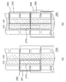
- a touch sensor panel 100 includes a touch detection area 120 in which a plurality of overlap sensing regions are arranged, a wiring area 130 that is provided outside the touch detection area 120, and a plurality of sensing electrodes 122 (i.e., a plurality of vertical electrodes C11 to C18 and a plurality of horizontal electrodes 11a to 15a and 11b to 15b) that are arranged in the touch detection area 120.
- a plurality of sensing electrodes 122 i.e., a plurality of vertical electrodes C11 to C18 and a plurality of horizontal electrodes 11a to 15a and 11b to 15b
- 'sensing region may not necessarily indicate an area physically or electrically separate from another region. Instead, the term 'sensing region' may indicate an area in which static capacitance varies in response to a touch input from a user.
- the touch detection area 120 may be an area in which a plurality of sensing electrodes 122 are arranged for sensing any touch location on a substrate 100.
- the wiring area 130 may account for the whole substrate 100 except for the touch detection area 120.
- a plurality of wires (i.e., a plurality of bus lines) 135 may be disposed in the wiring area 130.
- the wires 135 may connect the sensing electrodes 122 in the touch detection area 120 to a touch sensor circuit unit (not shown).
- the touch sensor circuit unit may sense and determine a touch location based on a variation in capacitance in the touch detection area 120 that results from the user's touch.
- each of the sensing electrodes 122 may have an extension line that may extend into the wiring area 130.
- wires C1 to C8 are connected to the vertical electrodes C11 to C18, and wires 11A to 15A and 11B to 15B are connected to the horizontal electrodes 11a to 15a and 11b to 15b, respectively.
- the wires 135 may serve as channels.
- the wires 135 may be formed on the substrate 100 at the same level as the sensing electrodes 122.
- the wires 135 may be disposed on a different level from the horizontal electrodes 11a to 15a and 11b to 15b or the vertical electrodes C11 to C18 and may be connected to the horizontal electrodes 11a to 15a and 11b to 15b and the vertical electrodes C11 to C18 through a plurality of vias.
- the wires 135 may be disposed on the substrate 100 at the same level as the horizontal electrodes 11a to 15a and 11b to 15b or the vertical electrodes C11 to C18.
- the wires 135 may be insulated from the horizontal electrodes 11a to 15a and 11b to 15b or the vertical electrodes C11 to C18 by depositing a dielectric material at each of the intersections between the wires 135 and the horizontal electrodes 11a to 15a and 11b to 15b or between the wires 135 and the vertical electrodes C11 to C18
- the vertical electrodes C11 to C18 may be disposed at horizontal locations X1 to X8, respectively, in the touch detection area 120, thereby forming a plurality of sensing regions.
- the vertical electrodes C11 to C18 may also form the sensing regions with other electrodes.
- the touch sensor circuit unit may determine the X-axis component of a touch location using the vertical electrodes C11 to C18.
- Each of the vertical electrodes C11 to C18 may include an extension line 141 that extends into the wiring area 130. In the example illustrated in FIG. 1, the extension lines 141 of the vertical electrodes C11 to C18 all extend into a wiring area that is provided below a panel (not shown).
- some of the extension lines 141 of the vertical electrodes C11 to C18 may extend into a wiring area that is provided above the panel.
- the vertical electrodes C11 to C18 may be connected to different wires.
- the vertical electrodes C11 to C18 may be connected to the wires C1 to C8, respectively.
- Some of the vertical electrodes C11 to C18 may be electrically connected to each other, as illustrated in FIG. 3.
- the vertical electrodes C11 to C18 may be formed as bars that extend in a vertical direction.
- the vertical electrodes C21 to C28 may be formed in various shapes, other than a bar shape, as long as they can form a regular pattern.
- the horizontal electrodes 11a and 11b, 12a and 12b, 13a and 13b, 14a and 14b, and 15a and 15b may be disposed at vertical locations Y1, Y2, Y3, Y4, and Y5, respectively, thereby forming a plurality of sensing regions.
- the horizontal electrodes 11a to 15a and 11b to 15b may form the sensing regions with other electrodes.
- the touch sensor circuit unit may determine the Y-axis component of a touch location by using the horizontal electrodes 11a to 15a and 11b to 15b.
- the horizontal electrodes 11a to 15a and 11b to 15b may be formed on the substrate 100 at the same level as the vertical electrodes C11 to C18 in the vicinity of the vertical electrodes C11 to C18.
- Each of the horizontal electrodes 11a to 15a and 11b to 15b may include a plurality of partitioning electrodes and an extension line 143 or 145 by which the partitioning electrodes are electrically connected to one another in the wiring area 130.
- the partitioning electrodes and the extension line 143 or 145 may be formed at the same time.
- the partitioning electrodes may be formed at the same time with a portion of the extension line 143 or 145.
- the vertical electrodes C11 to C18 and the horizontal electrodes 11a to 15a and 11b to 15b may be formed of a transparent conductive material, such as indium tin oxide (ITO), ZnO, indium zinc oxide (IZO), a carbon nanotube (CNT), or the like.
- the vertical electrodes C11 to C18 and the horizontal electrodes 11a to 15a and 11b to 15b may be formed of the same material.
- Some of the extension lines of the electrodes 11a to 15a and 11b to 15b may be formed of a metallic material to increase the conductivity of the horizontal electrodes 11a to 15a and 11b to 15b or the thermal resistance of the vertical electrodes C11 to C18 and the horizontal electrodes 11a to 15a and 11b to 15b in case the vertical electrodes C11 to C18 and the horizontal electrodes 11a to 15a and 11b to 15b are connected to external wirings through a plurality of vias.
- a part of the extension lines of the electrodes 11a to 15a and 11b to 15b in the touch detection area 120 may be formed of a transparent conductive material, and another part of the extension lines of the electrodes 11a to 15a and 11b to 15b outside the touch detection area 120 may be formed of silver, copper, or the like.
- the substrate 110 may be a transparent window.
- the transparent window may be formed of a highly rigid material such as tempered glass or an acrylic resin or a soft material that may be used to manufacture a flexible display, such as a polyethylene terephthalate (PET), polycarbonate (PC), polyesther sulfone (PES), polyimide (PI), polymethyl methacrylate (PMMA), or the like.
- PET polyethylene terephthalate
- PC polycarbonate
- PES polyesther sulfone
- PI polyimide
- PMMA polymethyl methacrylate
- the transparent window may maintain the external shape of the touch sensor panel 100. At least part of the transparent window may be exposed to the outside of the touch sensor panel 100, and may thus accommodate contacts with a conductive object, such as the user's body, a stylus pen, or the like.
- a protection layer (not shown) may be additionally provided.
- 'contact may indicate not only a direct contact by a conductive object with a contact-accommodating surface but also an indirect contact in which the conductive object approaches to the contact-accommodating surface to be in a close vicinity of the contact-accommodating surface. Accordingly, the terms 'touch sensor panel' and 'touch sensing apparatus equipped with a touch sensor panel' may be interpreted as a touch sensor panel capable of not only recognizing a conductive object's direct contact therewith but also detecting any approaching or nearby object.
- the sensing electrodes 122 may be formed on a separate substrate.
- the sensing electrodes 122 may be attached onto a transparent window by using an adhesive material such as an optical clear adhesive or the like. That is, the sensing electrodes 122 may be formed by patterning an ITO film, which is a PET or thin glass film having ITO formed on one or both surfaces thereof, and attaching the patterned ITO film onto a transparent window.
- the patterning of the ITO film may be performed by patterning one surface of the ITO film into the shape of the vertical electrodes C11 to C18 and patterning the other surface of the ITO film into the shape of the horizontal electrodes 11a to 15a and 11b to 15b.
- the patterned ITO film may be attached onto a transparent window such that the vertical electrodes C11 to C18 may be disposed between the patterned ITO film and the transparent window.
- the vertical electrodes C11 to C18 and the horizontal electrodes 11a to 15a and 11b to 15b may be formed in one body with a transparent window 110 by patterning one surface of the transparent window 110 into the shapes of the vertical electrodes C11 to C18 and the horizontal electrodes 11a to 15a and 11b to 15b. Because, in this example, a process of attaching the sensing electrodes 122 onto the transparent window 110, which often results in a high defect rate, is not performed, it is possible to simplify the manufacture of a touch sensor panel, improve the manufacture yield of a touch sensor panel, reduce the manufacturing cost of a touch sensor panel, and reduce the thickness of an electronic device to which a touch sensor panel is applied.
- one body may indicate forming an element directly on another element without the aid of an additional adhesive layer.
- the sensing electrodes 122 may be interpreted as being formed directly on one surface of the transparent window 110 without the aid of an adhesive layer such as an OCA or the like. That is, the sensing electrodes 122 may be directly formed on the transparent window 110 through sputtering, ion plating, etching, or the like, instead of forming the sensing electrodes 122 on a separate element such as an ITO film, and attaching the ITO film onto the transparent window 110.
- the sensing electrodes 122 may be formed using various methods as long as they do not involve a process of attaching the sensing electrodes 122 onto the transparent window 110.
- the sensing electrodes 122 may be formed by directly patterning an exposed surface of the transparent window 110 or may be directly formed on a transparent window coated with an additional layer, such as an anti-scatter film, a transparent resin, or the like.
- the sensing electrodes 122 may all be formed at once in one body with the transparent window 110.
- the sensing electrodes 122 may also be formed in one body with the transparent window 110 in multiple stages.
- the sensing electrodes 122 may be formed by forming the vertical electrodes C11 to C18 on one surface of the transparent window 110, coating the transparent window 110 with a dielectric layer, and forming the horizontal electrodes 11a to 15a and 11b to 15b on the dielectric layer.
- only some of the sensing electrodes 122 may be formed in one body with the transparent window 110.
- the vertical electrodes C11 to C18 may be formed in one body with the transparent window 110
- the horizontal electrodes 11a to 15a and 11b to 15b may be formed on an ITO film
- the ITO film may be attached onto the transparent window 110.
- the vertical electrodes C11 to C18 may be classified into one or more groups and may be arranged in units of the groups such that at least a pair of vertical electrodes included in each of the groups may be adjacent to each other.
- the touch sensor panel 100 is a mutual capacitance touch sensor panel
- the vertical electrodes C11 to C18 may be classified into four groups, each group having a pair of vertical electrodes, and may be arranged such that a pair of vertical electrodes in each of the groups may be adjacent to each other.
- the vertical electrodes C11 to C18 may be evenly spaced to precisely determine a touch location in a horizontal direction.
- the vertical electrodes C11 to C18 may be electrically insulated from one another by being connected to the wires C1 to C8, respectively.
- a pair of neighboring vertical electrodes having a pair of partitioning electrodes interposed therebetween may be electrically connected to each other to reduce the number of channels required. That is, the vertical electrodes C12 and C13 may be electrically connected, the vertical electrodes C14 and C15 may be electrically connected, and the vertical electrodes C16 and C17 may be electrically connected. In this manner, it is possible to reduce the number of channels from eight (ranging from C1 to C8 in the example illustrated in FIG.
- At least two of the horizontal electrodes 11a to 15a and 11b to 15b may be arranged to pass through a horizontal axis at an arbitrary position.
- the horizontal electrode 11a on a Y-axis location Y1 which includes a plurality of partitioning electrodes 151, 153, 155, and 157 that are disposed at a plurality of odd-numbered X-axis locations X1, X3, X5, and X7, respectively
- the horizontal electrode 11b on the Y-axis location Y1 which includes a plurality of partitioning electrodes 152, 154, 156, and 158 that are disposed at a plurality of even-numbered X-axis locations X2, X4, X6, and X8, respectively, may share a Y axis corresponding to the Y-axis location Y1.
- the horizontal electrodes 11a and 11b may be arranged such that a central horizontal axis that horizontally divides the horizontal electrode 11a into halves may coincide with a central horizontal axis that horizontally divides the horizontal electrode 11b into halves. That is, the orthogonal projection of the horizontal electrode 11a with respect to the Y axis may substantially overlap the orthogonal projection of the horizontal electrode 11b with respect to the Y axis.
- the horizontal electrodes 11a to 15a and 11b to 15b may be divided into two groups, i.e., a first horizontal electrode group 10A including the horizontal electrodes 11a to 15a, which are disposed on the left side of their respective pairs of vertical electrodes, and a second horizontal electrode group 10B including the horizontal electrodes 11b to 15b, which are disposed on the right side of their respective pairs of vertical electrodes.
- the partitioning electrodes of each of the horizontal electrodes 11a to 15a and 11b to 15b may be evenly spaced.
- FIG. 1 referring to FIG.
- the horizontal electrodes 11a to 15a and 11b to 15b may be arranged such that two of the partitioning electrodes of each of the horizontal electrodes 11a to 15a and 11b to 15b may be more adjacent to each other than to the other partitioning electrodes.
- the horizontal electrodes 11a to 15a and 11b to 15b may be arranged such that some of the partitioning electrodes of each of the horizontal electrodes 11a to 15a and 11b to 15b may be more adjacent to each other than the other partitioning electrodes, and that the other partitioning electrodes may be evenly spaced.
- a driving signal may be applied to at least one of the vertical electrodes C11 to C18 and/or the first and second horizontal electrode groups 10A and 10B.
- electric field lines i.e., leakage fluxes
- a partitioning electrode and a pair of sectors of a vertical electrode that is adjacent to or in the vicinity of the partitioning electrode may form a sensing region whose charge can be coupled from a driving area to a sensing electrode.
- the touch sensor panel 100 is a mutual capacitance touch sensor panel, unless specified otherwise (i.e., unless specified as, for example, a self-capacitance touch sensor panel), that the first and second horizontal electrode groups 10A and 10B are driving electrode groups to which a driving signal is applied, and that the vertical electrodes C11 to C18 are sensing electrodes for detecting a sensing signal.
- FIG. 4 illustrates enlarged views of a portion 151 of the touch detection area 120 where a plurality of sensing regions are formed.
- a partitioning electrode and a particular sector of a vertical electrode may account for parts of two or more sensing regions.
- the touch sensor circuit unit of the touch sensor panel 100 may precisely determine a touch location by extracting a horizontal location component and a vertical location component of the touch input from a plurality of overlapping sensing regions and combining the extracted horizontal and vertical location components.
- a first sensing region 171 may be formed by a first partitioning electrode 161 of the horizontal electrode 14a and a first sensing sector 166 of the vertical electrode C15
- a second sensing region 172 may be formed by the first partitioning electrode 161 and a second sensing sector 167 of the vertical electrode C16
- a third sensing region 173 may be formed by a second partitioning electrode 162 of the horizontal electrode 14b and the second sensing sector 167 of the vertical electrode C16
- a fourth sensing region 174 may be formed by the second partitioning electrode 162 and the first sensing sector 166 of the vertical electrode 15.
- the first and fourth sensing regions 171 and 174 may share the first sensing sector 166.
- the first and second partitioning electrodes 161 and 162 and the first and second sensing sectors 166 and 167 may be used to extract the horizontal and vertical components of a touch location. Because there is an overlap between the first to fourth sensing regions 171 to 174, the touch sensor circuit unit may precisely determine a touch location by combining mutual capacitance variations detected from the first to fourth sensing regions 171 to 174, particularly from the vertical electrodes C15 and C16.
- the plurality of sensing regions including one or more overlap sensing regions (such as first to fourth sensing regions 171 to 174) therebetween, as illustrated in FIG. 4, are arranged along a horizontal direction to overlap one another.
- the overlap sensing regions may be configured to be arranged along a vertical direction or a diagonal direction or to be arranged in the same row with a partitioning electrode interposed therebetween.
- FIG. 5 illustrates plot views taken along line T-T' of FIG. 1 for explaining mutual capacitance that is measured along the cross-section of the portion 151 of the touch detection area 120. More specifically, FIG. 5 illustrates the variation of mutual capacitance detected by the first and second sensing sectors 166 and 167 of the vertical electrodes C15 and C16 according to the location of a finger in a case in which the first partitioning electrode 161 of the horizontal electrode 14a, the first sensing sector 166, the second sensing sector 167, and the second partitioning electrode 162 of the horizontal electrode 14b are sequentially arranged in an overlap sensing region 151.
- a cover glass 112 which is a type of substrate, may be disposed over the first partitioning electrode 161, the first sensing sector 166, the second sensing sector 167, and the second partitioning electrode 162.
- the first and second partitioning electrodes 161 and 162 serve as driving electrodes
- the first and second sensing sectors 166 and 167 serve as sensing electrodes.
- FIGS. 5(a) and 5(b) illustrate a case in which an object (for example, a finger) that is placed in contact with the touch sensor panel 100 is located between the first driving electrode 161 and the first sensing electrode 166.
- an object for example, a finger
- FIG. 5(a) when a driving signal is applied to the first driving electrode 161, a mutual capacitance variation of 100 may be detected from the first sensing electrode 166, which is adjacent to the first driving electrode 161, and a mutual capacitance variation of 20 may be detected from the second sensing electrode 167, which neighbors the first sensing electrode 166.
- a driving signal may be applied to the second driving electrode 162 immediately after the application of a driving signal to the first driving electrode 161.
- a mutual capacitance variation of 5 may be detected from the first sensing electrode 166, and no mutual capacitance variation may be detected from the second sensing electrode 167, which is distant apart from the finger.
- FIG. 5(c) illustrates mutual capacitance measurements in piles obtained from the first and second sensing electrodes 166 and 167 by applying a driving signal to the first sensing electrode 166 and then to the second sensing electrode 167 in a case in which the finger is placed closer to the first sensing electrode 166 than to the second sensing electrode 167.
- a mutual capacitance variation of 60 may be detected from the first sensing electrode 166
- a mutual capacitance variation of 30 may be detected from the second sensing electrode 167.
- FIG. 5(d) illustrates mutual capacitance measurements in piles obtained from the first and second sensing electrodes 166 and 167 in a case in which the finger is located between the second sensing electrode 167 and the second driving electrode 162.
- a mutual capacitance variation of 105 may be detected from the second sensing electrode 167 in the vicinity of the finger, and a mutual capacitance variation of 20 may be detected from the first sensing electrode 166 that is more distant than the second sensing electrode 167 from the finger.
- FIG. 13 is a diagram for explaining the concept of linearity.
- Linearity may indicate how precisely pairs of diagonal positions can be detected in response to the receipt of a diagonal 'sliding' touch input across the touch sensor panel 100. The closer the detected diagonal position pairs are to a diagonal line, the higher the linearity.
- FIG. 14(a) illustrates a case in which a diagonal 'sliding' touch input is detected across the touch sensor panel 100
- FIGS. 14(b) and 14(c) illustrate the detection of diagonal position pairs in response to the detection of the diagonal 'sliding' touch input. Linearity is higher in the example illustrated in FIG. 14(c) than in the example illustrated in FIG. 14(b).
- a driving signal may be randomly applied to each of the horizontal electrodes 11a to 15a and 11b to 15b.
- a driving signal may be sequentially applied to the horizontal groups (i.e., the horizontal electrodes 11a to 15a) included in the first horizontal electrode group 10A, and then to the horizontal groups (i.e., the horizontal electrodes 11b to 15b) included in the second horizontal electrode group 10B.
- a driving signal may be sequentially applied to a plurality of rows of horizontal electrodes (for example, in the order of 11a, 11b, 12a, 12b, ).
- a driving signal may be sequentially applied to a number of driving electrodes that are adjacent to one another in a diagonal direction (for example, in the order of 11a, 12b, 13a, 14b, ).
- the first partitioning electrode 161 and the first sensing sector 166 in the first sensing region 171 may have substantially the same area.
- the marginal area between the first partitioning electrode 161 and the first sensing sector 166 may be enlarged so that a leakage electric field may increase, and that the difference between the areas of the first partitioning electrode 161 and the first sensing sector 166 may be offset by the marginal area.
- the width of the boundary area of each electrode may be reduced, the vertical electrodes C11 to C18 may be formed so as to form a periodic geometric pattern, and the horizontal electrodes 11a to 15a and 11b to 15b may be formed to fill the areas occupied by the vertical electrodes C11 to C18.
- the periodic geometric pattern may have a triangular or rectangular shape.
- the plurality of sensing sectors in any one of the vertical electrodes C11 to C18 are electrically connected to one anther in the touch detection area 120, and may thus operate as sensing electrodes. Sensing electrodes may be required to be robust against noise or signals. In the touch sensor panel 100, noise may be generated mainly by a driving signal, which is applied to driving electrodes, and the circuitry in a digital device to which the touch sensor panel 100 is attached.
- the influence of noise caused by a driving signal on the vertical electrodes C11 to C18 may be reduced by arranging wires in such a manner that each wire which provides the driving signal to a driving electrode may be as distant as possible from sensing electrodes. For example, referring to FIGS.
- extension lines 902a, 903a, 904a, and 905a that extend from the first horizontal electrode group 10A including the horizontal electrodes 11a to 15a, which are located on the left side of the vertical electrode C13, may be arranged on the left side of the first horizontal electrode group 10A
- extension lines 902b, 903b, 904b, and 905b that extend from the second horizontal electrode group 10B including the horizontal electrodes 11b to 15b, which are located on the right side of the vertical electrode C12 may be arranged on the right side of the second horizontal electrode group 10B.
- the first and second horizontal electrode groups 10A and 10B may serve as noise protectors against a driving signal.
- driving electrodes can serve as noise protectors
- driving electrodes may be arranged along the edge of a substrate.
- some of the horizontal electrodes included in the first horizontal electrode group 10A may be arranged on the outermost left side of the touch detecting area 120
- some of the horizontal electrodes included in the second horizontal electrode group 10B may be arranged on the outermost right side of the touch detecting area 120.
- a noise generated by a display may be compensated by a touch controller that interprets signals detected from a touch detection area using a program.
- a noise may be generated even by a slight capacitance variation that may result from an external shock-induced misalignment between a touch detection area and a display. This type of noise may be reduced using a shield layer that may be disposed between a digital device and the touch sensor panel 100.
- the shield layer will be described later in detail with reference to FIG. 15.
- the touch sensor panel 100 may operate not only as a mutual capacitance touch sensor panel but also as a self-capacitance touch sensor panel.
- a reference ground plane may be formed on the rear surface of a given substrate, on the same surface of the given substrate where the vertical electrodes C11 to C18 and the first and second horizontal electrode groups 10A and 10B are arranged to be separate from each other by a dielectric material, or on the surface of a separate substrate.
- Each sensing region in a self-capacitance touch sensor panel may have a self capacitance with respect to a reference ground that may vary in response to the existence of an object in the vicinity of the self-capacitance touch sensor.
- each of the vertical electrodes C11 to C18 and the horizontal electrodes included in each of the first and second horizontal electrode groups 10A and 10B may sense a self-capacitance independently.
- FIG. 7 is a plan view illustrating part of a touch sensor panel 200 according to another exemplary embodiment.
- the touch sensor panel 200 is different from the touch sensor panel 100 illustrated in FIG. 1 in that at least two of a plurality of horizontal electrodes are arranged to pass through a horizontal axis at an arbitrary position and to have their central axes misaligned with each other.
- like reference numerals indicate like elements, and thus, repetitive descriptions thereof will be omitted.
- the touch sensor panel 200 includes a touch detection area 220 in which a plurality of overlap sensing regions are arranged, a wiring area 130 that is provided outside the touch detection area 220, and a plurality of vertical electrodes C21 to C28 and a plurality of horizontal electrodes 21a, 21b, 22a, 22b, 23a, 23b, 24a, and 24b that are arranged on the touch detection area 220.
- the touch detection area 220 may be an area for detecting a touch location on the touch sensor panel 200.
- the wiring area 130 may be an area provided outside the touch detection area 220.
- a plurality of wires (e.g., bus lines) 235 that connect the electrodes C21 to C28, 21a, 21b, 22a, 22b, 23a, 23b, 24a, and 24b and a touch sensor circuit unit (not shown) may be formed in the wiring area 130.
- the touch sensor circuit unit may detect and determine a touch location in the touch detection area 220 based on a capacitance variation resulting from a user's touch on the touch sensor panel 200.
- the extension lines of the sensing electrodes in the touch detection area 220 may extend into the wiring area 130.
- wires in the wiring area 130 may be electrically connected to the vertical electrodes C21 to C28, respectively, and some of the wires in the wiring area 130, for example, wires 21A to 24A and 21B to 24B, may be electrically connected to the horizontal electrodes C21 to C28, respectively.
- the wires in the wiring area 130 may serve as channels 235.
- the wires in the wiring area 130 may be formed of a metallic material, and may be formed on the substrate 200 at the same level.
- the wires in the wiring area 130 may be disposed on the substrate 200 at a different level from the horizontal electrodes 21a to 24a and 21b to 24b or the vertical electrodes C21 to C28, and may be connected to the horizontal electrodes 21a to 24a and 21b to 24b or the vertical electrodes C21 to C28 through a plurality of vias.
- the wires in the wiring area 130 may be disposed on the substrate 200 at the same level as the horizontal electrodes 21a to 24a and 21b to 24b or the vertical electrodes C21 to C28. In this case, the intersections between the wires in the wiring area 130 and the horizontal electrodes 21a to 24a and 21b to 24b or the vertical electrodes C21 to C28 may be coated with a dielectric material so as to prevent unnecessary electric contacts.
- the vertical electrodes C21 to C28 may be disposed at a plurality of horizontal locations X1 to X8, respectively, in the touch detection area 120, thereby forming a plurality of sensing regions.
- One of the vertical electrodes C21 to C28 may mutually form a sensing region with other electrodes.
- the touch sensor circuit unit may determine the X-axis component of a touch location using the vertical electrodes C21 to C28.
- Each of the vertical electrodes C21 to C28 may include an extension line 241 that extends into the wiring area 130.
- the extension lines 241 of the odd-numbered vertical electrodes C21, C23, C25, and C27 may extend into a wiring area that is provided below a panel
- the extension lines 241 of the even-numbered vertical electrodes C22, C24, C26, and C28 may extend into a wiring area that is provided above the panel (not shown).
- the vertical electrodes C21 to C28 may be connected to different wires via the extension lines 241.
- the vertical electrodes C21 and C23 may be connected to the wires CC1 and CC3, respectively.
- the vertical electrodes C21 to C28 may be formed as bars that extend in a vertical direction.
- the vertical electrodes C21 to C28 may be formed in various shapes, other than a bar shape, as long as they can form a regular pattern.
- the horizontal electrodes 21b, 21a, 22b, 22a, 23b, 23a, 24b, and 24a may be disposed at vertical locations Y1, Y2, Y3, Y4, Y5, Y6, Y7, and Y8, thereby forming a plurality of sensing regions.
- One of the horizontal electrodes 21a to 24a and 21b to 24b may form a sensing region with other electrodes.
- the touch sensor circuit unit may determine the Y-axis component of a touch location by using the horizontal electrodes 21a to 24a and 21b to 24b.
- the horizontal electrodes 21a to 24a and 21b to 24b may be formed on the substrate at the same level as the vertical electrodes C21 to C28 in the vicinity of the vertical electrodes C21 to C28.
- Each of the horizontal electrodes 21a to 24a and 21b to 24b may include a plurality of partitioning electrodes and an extension line 243 or 245 by which the partitioning electrodes are electrically connected to one another in the wiring area 130.
- the partitioning electrodes and the extension line 243 or 245 may be formed at the same time.
- the partitioning electrodes may be formed at the same time with a portion of the extension line 243 or 245.
- At least two of the horizontal electrodes 21a to 24a and 21b to 24b may be arranged to pass through a horizontal axis at an arbitrary position and to have their central axes misaligned with each other.
- the horizontal electrode 22a including a plurality of partitioning electrodes 251, 253, 255, and 257 disposed at the odd-numbered X-axis locations X1, X3, X5, and X7, respectively, and at the Y-axis location Y4, and the horizontal electrode 22b, which includes a plurality of partitioning electrodes 252, 254, 256, and 258 that are disposed at a plurality of the even-numbered X-axis locations X2, X4, X6, and X8, respectively, and the Y-axis location Y3 may share an arbitrary Y axis 290.
- the horizontal electrodes 22a and 22b may be arranged such that a central horizontal axis (i.e., Y4) that horizontally divides the horizontal electrode 22a into halves may not coincide with a central horizontal axis (i.e., Y3) that horizontally divides the horizontal electrode 22b into halves.
- the horizontal electrodes 21a to 24a and 21b to 24b may be classified into a first group 20A including the horizontal electrodes 21a to 24a, which are disposed on the left side of their respective vertical electrodes, and a second group 20B including the horizontal electrodes 21b to 24b, which are disposed on the right side of their respective vertical electrodes.
- FIG. 8 illustrates a plurality of sensing regions that are formed in a portion 280 of the touch sensor panel 200.
- the touch sensor panel 200 operates as a mutual capacitance touch sensor panel.
- some of the partitioning electrodes of the horizontal electrode 23a may form a first sensing region 281 with part of the vertical electrode C25, and may form a second sensing region 282 with part of the vertical electrode C26.
- some of the partitioning electrodes of the horizontal electrode 24b may form a third sensing region 283 with part of the vertical electrode C26, and may form a fourth sensing region 284 with part of the vertical electrode C25.
- some of the partitioning electrodes of the horizontal electrode 23b may form a fifth sensing region 285 with part of the vertical electrode C26, and may form a sixth sensing region 286 with part of the vertical electrode C25.
- the first, fourth, and sixth sensing regions 281, 284, and 286 may overlap at least part of a sensing sector 270. Because there is an overlap between a plurality of sensing regions, it is possible to improve sensing resolution and linearity.
- FIG. 9 is an enlarged top view of the portion 280 of the touch sensor panel 200.
- the touch sensor panel 200 operates as a mutual capacitance touch sensor panel.
- reference characters A and B indicate points of contact with an object, such as a finger.
- the vertical electrode C25 or C26 may detect the same mutual capacitance drop from locations A and B.
- the vertical electrode C25 or C26 may detect a considerable mutual capacitance drop only when the finger is located at location B.
- the touch sensor panel 200 can precisely determine a Y coordinate of a touch location with the use of fewer driving electrodes, as compared to a related-art touch sensor panel. Therefore, it is possible to maintain a high resolution while reducing the number of channels required.
- FIG. 10 is a plan view illustrating part of a touch sensor panel according to another exemplary embodiment.
- the touch sensor panel illustrated in FIG. 10 is different from the touch sensor panel 200 illustrated in FIG. 7 in that each of the vertical electrodes thereof forms a series of triangular patterns.
- FIG. 11 is enlarged top views of portion 320 of the touch sensor panel illustrated in FIG. 10.
- the touch sensor panel illustrated in FIG. 10 includes a plurality of vertical electrodes C31 to C36 and a first group of horizontal electrodes 31a and 32a and a second group of horizontal electrodes 31b, 32b, and 33b.
- the left side of the vertical electrode C31 may extend in a zigzag manner along a vertical direction and the right side of the vertical electrode C31 may extend straight along the vertical direction, thereby forming a series of triangular patterns that face toward the left.
- the left side of the vertical electrode C32 which is formed on the right side of the vertical electrode C31, may extend straight along the vertical direction and the right side of the vertical electrode C32 may extend in a zigzag manner along the vertical direction, thereby forming a series of triangular patterns that face toward the right.
- the vertical electrodes C31 and the vertical electrode C32 may be aligned such that they may be misaligned with each other. Instead, the vertical electrode C31 may be aligned with the vertical electrodes C33 and C35, and the vertical electrode C32 may be aligned with the vertical electrodes C34 and C36.
- the horizontal electrodes in the first group and the horizontal electrodes in the second group may be arranged along the vertical direction.
- the horizontal electrodes in the first group i.e., the horizontal electrodes 31a and 32a
- the horizontal electrodes in the second group i.e., the horizontal electrodes 31b, 32b, and 33b
- the horizontal electrodes 31b, 32b, and 33b may be arranged on the right side of their respective even-numbered vertical electrodes, and may be spaced apart from the right side of their respective even-numbered vertical electrodes by a predetermined distance.
- Each of the horizontal electrodes 31a and 32a and 31a to 33b may include an extension line through which they may be electrically connected to outside a touch detection area.
- FIG. 11 illustrates a plurality of overlap sensing regions that may be formed in the portion 320 of the touch sensor panel illustrated in FIG. 10.
- first through fourth sensing regions 331 to 334 may be formed in connection with a sensing sector 340.
- the sensing sector 340 may detect multiple mutual capacitance variations in response to the application of a driving signal.
- a touch sensor circuit unit (not shown) of the touch sensor panel illustrated in FIG. 10 may precisely determine a touch location by overlapping or combining a plurality of sensing signals.
- a long separation line 315 may be formed in a sensing region 310, and thus, a leakage electric current may increase. Therefore, the intensity of the sensing signal detecting a mutual capacitance variation may increase, and thus, the precision of touch sensing may increase, as compared to a touch sensor panel having no such electrode pattern.
- a driving electrode and a sensing electrode that form a sensing region together may not necessarily have the same area.
- the difference between the area of the driving electrode and the area of the sensing electrode may be reduced by narrowing a width d1 of the separation line between the driving electrode and the sensing electrode and a width d2 of the extension line of the driving electrode.
- the touch sensor circuit unit of the touch panel sensor illustrated in FIG. 10 may improve the linearity of the detection of a touch input.
- FIG. 12 is a plan view illustrating part of a touch sensor panel according to another exemplary embodiment.
- the touch sensor panel illustrated in FIG. 12 is different from the touch sensor panel 200 illustrated in FIG. 7 and the touch sensor panel illustrated in FIG. 10 in that the vertical electrodes thereof are each formed in the shape of a comb.
- a first group of horizontal electrodes 41a to 43a and a second group of horizontal electrodes 41b to 43b may be arranged such that the central horizontal axes of the horizontal electrodes 41a to 43a may be misaligned with the central horizontal axes of the horizontal electrodes 41b to 43b.
- a central horizontal axis 410 of the horizontal electrode 42a may be misaligned with a central horizontal axis 420 of the horizontal electrode 42b.
- the horizontal electrode 42a may include four patches 431 to 434.
- the detection of a touch location in or near each of the patches 431 to 434 may be performed by combining a plurality of sensing signals sensed from a vertical electrode adjacent to a corresponding patch and to which a driving signal is provided.
- the location of the finger may be determined by combining a sensing signal resulting from the application of a driving signal to the horizontal electrode 43a and a sensing signal resulting from the application of a driving signal to the horizontal electrode 42b.
- the location of the finger may be determined by combining a sensing signal resulting from the application of a driving signal to the horizontal electrode 42b and a sensing signal resulting from the application of a driving signal to the horizontal electrode 41b.
- the location of the finger may be determined by combining a sensing signal resulting from the application of a driving signal to the horizontal electrode 41b and a sensing signal resulting from the application of a driving signal to the horizontal electrode 41a.
- the combination of sensing signals sensed when an object, such as a finger, is located in the portion 442 may be distinguished from the combination of sensing signals sensed when the finger is located in the portion 443 because a mutual capacitance variation resulting from the application of a driving signal to the horizontal electrode 42b, which is horizontally adjacent to the portion 442, is larger than a mutual capacitance variation resulting from the application of a driving signal to the horizontal electrode 41b, which is diagonally adjacent to the portion 442.
- FIG. 13 is a plan view illustrating part of a touch sensor panel according to another exemplary embodiment.
- the touch sensor panel illustrated in FIG. 13 is different from the touch sensor panel 200 illustrated in FIG. 7 in that each of the horizontal electrodes includes two trapezoidal protrusions connected to each other.
- the touch sensor panel illustrated in FIG. 13 includes two groups of horizontal electrodes, i.e., horizontal electrodes 51a to 53a and horizontal electrodes 51b to 53b, and each of the horizontal electrodes 51a to 53a and 51b to 53b may be formed in a shape obtained by combining two trapezoidal protrusions.
- the touch sensor panel illustrated in FIG. 13 also includes a plurality of vertical electrodes C51 to C58.
- the vertical electrodes C51 to C58 may be formed to conform to the shape of their respective horizontal electrodes.
- FIG. 15 illustrates exploded and plan views illustrating a touch sensor panel including a shield layer according to another exemplary embodiment.
- a touch sensor panel 530 may be disposed on a digital device 510.
- the touch sensor panel 530 may include a touch detecting portion 560, which is formed on one surface of an external substrate 570, and a shield layer 540, which is formed at the bottom of the touch detecting portion 560.
- the external substrate 570 may serve as a surface of contact with a user or as a supporting substrate for the touch detecting portion 560.
- the external substrate 570 may be formed of a material having a uniform dielectric constant, and may be configured to have a predetermined thickness.
- a plurality of sensing electrodes capable of detecting any contact with the user may be arranged on the touch detecting portion 560.
- the touch detecting portion 560 may be formed in one body with the external substrate 570, or may be attached onto the external substrate 570 using an adhesive layer.
- the touch sensor panel 530 may be installed on the outermost surface of the digital device 510 and may thus be able to be contacted by the user. Furthermore, the touch sensor panel 530 may be electrically affected by circuitry in the digital device 510. For example, in a case in which the touch sensor panel 530 is a touchpad panel, an electrical noise from the electric circuitry at the bottom of the touch sensor panel 530 may infiltrate into the touch sensor panel 530. Alternatively, in a case in which the touch sensor panel 530 is a touch screen panel, electrical noises generated not only from the electric circuitry at the bottom of the touch sensor panel 530 but also from a display device may infiltrate into the touch sensor panel 530.
- a noise may also be generated due to even a minute capacitance variation resulting from a slight misalignment between the touch detecting portion 560 and a display device that may be caused by an external shock applied to a transparent window.
- the shield layer 540 may prevent the touch detection portion 560 from malfunctioning due to such electrical noises, and may thus improve the performance of the touch sensor panel 530.
- the shield layer 540 may include a substrate 541, which is formed of, for example, PET, and a conductive thin layer 543, which is formed on the substrate 541 by using a conductive material, such as ITO.
- the conductive thin layer 543 may substantially block electrical noises.
- the conductive thin layer 543 may be connected to a ground source to properly serve as an electrical shield.
- the shield layer 540 may also include wires 545 that connect the conductive thin layer 543 to the ground source.
- the wires 545 may be formed of a metallic material, such as silver.
- the shield layer 540 may also include a transparent adhesive layer 547 that attaches the shield layer 540 onto the touch detecting portion 560.
- the transparent adhesive layer 547 may be formed of, for example, an optical clear adhesive (OCA).
- An attachment unit 515 may be formed along the boundaries of the digital device 510 so that an air gap 520 may be formed between the touch sensor panel 530 and the digital device 510 when the touch sensor panel 530 is attached onto the digital device 510.
Abstract
L'invention concerne un panneau tactile utilisé pour un dispositif d'affichage. Le panneau tactile peut déterminer de façon précise un emplacement de touche a l'aide d'une zone donnée d'électrodes, peut réduire le nombre de canaux requis et peut réduire l'influence du bruit. De plus, le panneau tactile peut améliorer la résolution de la détection a l'aide d'un nombre donné de canaux d'électrode, peut être efficace contre le bruit et peut améliorer la linéarité par détermination précise d'un emplacement de touche.
Priority Applications (3)
| Application Number | Priority Date | Filing Date | Title |
|---|---|---|---|
| CN201280030231.6A CN103649882B (zh) | 2011-06-20 | 2012-01-12 | 触摸感应面板 |
| EP12171666.6A EP2538313B1 (fr) | 2011-06-20 | 2012-06-12 | Panneau de capteur tactile |
| US13/540,861 US9063621B2 (en) | 2011-06-20 | 2012-07-03 | Touch sensor panel |
Applications Claiming Priority (4)
| Application Number | Priority Date | Filing Date | Title |
|---|---|---|---|
| KR10-2011-0059814 | 2011-06-20 | ||
| KR1020110059814A KR101293165B1 (ko) | 2011-06-20 | 2011-06-20 | 접촉 감지 패널 |
| KR10-2011-0066953 | 2011-07-06 | ||
| KR20110066953 | 2011-07-06 |
Related Child Applications (1)
| Application Number | Title | Priority Date | Filing Date |
|---|---|---|---|
| US13/540,861 Continuation US9063621B2 (en) | 2011-06-20 | 2012-07-03 | Touch sensor panel |
Publications (1)
| Publication Number | Publication Date |
|---|---|
| WO2012176966A1 true WO2012176966A1 (fr) | 2012-12-27 |
Family
ID=47422772
Family Applications (1)
| Application Number | Title | Priority Date | Filing Date |
|---|---|---|---|
| PCT/KR2012/000292 WO2012176966A1 (fr) | 2011-06-20 | 2012-01-12 | Panneau tactile |
Country Status (2)
| Country | Link |
|---|---|
| CN (1) | CN103649882B (fr) |
| WO (1) | WO2012176966A1 (fr) |
Cited By (4)
| Publication number | Priority date | Publication date | Assignee | Title |
|---|---|---|---|---|
| CN103914193A (zh) * | 2013-01-09 | 2014-07-09 | 苏州市健邦触摸屏技术有限公司 | 一种电容式触摸屏 |
| CN104166487A (zh) * | 2013-05-15 | 2014-11-26 | 麦孚斯公司 | 使用单层感应图形的触摸传感装置及其制造方法 |
| TWI489364B (zh) * | 2013-08-23 | 2015-06-21 | Pixart Imaging Inc | 具雜訊屏蔽功能的電容式觸控感測裝置 |
| KR20150077161A (ko) * | 2013-12-27 | 2015-07-07 | 엘지디스플레이 주식회사 | 터치스크린 일체형 표시장치 |
Families Citing this family (5)
| Publication number | Priority date | Publication date | Assignee | Title |
|---|---|---|---|---|
| CN105094468A (zh) * | 2014-04-24 | 2015-11-25 | 敦泰科技有限公司 | 一种触摸屏设备及其单层互电容触摸屏体和电子装置 |
| CN105867673A (zh) * | 2015-01-23 | 2016-08-17 | 晶门科技(深圳)有限公司 | 触摸传感器面板及其制造方法 |
| TWI602093B (zh) * | 2016-02-04 | 2017-10-11 | 威達高科股份有限公司 | 觸控面板之線路佈局結構 |
| US11852925B2 (en) | 2019-07-25 | 2023-12-26 | Beijing Boe Technology Development Co., Ltd. | Display panel and display device having spacers with different heights |
| WO2021047122A1 (fr) * | 2019-09-10 | 2021-03-18 | 神盾股份有限公司 | Système de détection d'empreinte digitale prenant en charge un mode capacitif et un mode ultrasonore, et procédé de reconnaissance d'image d'empreinte digitale associé |
Citations (4)
| Publication number | Priority date | Publication date | Assignee | Title |
|---|---|---|---|---|
| US20090091551A1 (en) * | 2007-10-04 | 2009-04-09 | Apple Inc. | Single-layer touch-sensitive display |
| KR20100126140A (ko) * | 2009-05-21 | 2010-12-01 | (주)에릭소코퍼레이션 | 정전용량방식 터치패널의 전극패턴구조 |
| JP2011018177A (ja) * | 2009-07-08 | 2011-01-27 | Hosiden Corp | 静電容量型タッチセンサ |
| JP2011039662A (ja) * | 2009-08-07 | 2011-02-24 | Sanyo Electric Co Ltd | 静電容量型入力装置 |
Family Cites Families (4)
| Publication number | Priority date | Publication date | Assignee | Title |
|---|---|---|---|---|
| KR100885730B1 (ko) * | 2007-03-05 | 2009-02-26 | (주)멜파스 | 단순한 적층 구조를 갖는 접촉위치 감지 패널 |
| US20100059294A1 (en) * | 2008-09-08 | 2010-03-11 | Apple Inc. | Bandwidth enhancement for a touch sensor panel |
| US8749496B2 (en) * | 2008-12-05 | 2014-06-10 | Apple Inc. | Integrated touch panel for a TFT display |
| US20110048813A1 (en) * | 2009-09-03 | 2011-03-03 | Esat Yilmaz | Two-dimensional position sensor |
-
2012
- 2012-01-12 CN CN201280030231.6A patent/CN103649882B/zh active Active
- 2012-01-12 WO PCT/KR2012/000292 patent/WO2012176966A1/fr active Application Filing
Patent Citations (4)
| Publication number | Priority date | Publication date | Assignee | Title |
|---|---|---|---|---|
| US20090091551A1 (en) * | 2007-10-04 | 2009-04-09 | Apple Inc. | Single-layer touch-sensitive display |
| KR20100126140A (ko) * | 2009-05-21 | 2010-12-01 | (주)에릭소코퍼레이션 | 정전용량방식 터치패널의 전극패턴구조 |
| JP2011018177A (ja) * | 2009-07-08 | 2011-01-27 | Hosiden Corp | 静電容量型タッチセンサ |
| JP2011039662A (ja) * | 2009-08-07 | 2011-02-24 | Sanyo Electric Co Ltd | 静電容量型入力装置 |
Cited By (6)
| Publication number | Priority date | Publication date | Assignee | Title |
|---|---|---|---|---|
| CN103914193A (zh) * | 2013-01-09 | 2014-07-09 | 苏州市健邦触摸屏技术有限公司 | 一种电容式触摸屏 |
| CN104166487A (zh) * | 2013-05-15 | 2014-11-26 | 麦孚斯公司 | 使用单层感应图形的触摸传感装置及其制造方法 |
| US9501187B2 (en) | 2013-05-15 | 2016-11-22 | Melfas Inc. | Touch sensing apparatus using single layer pattern and method for manufacturing the same |
| TWI489364B (zh) * | 2013-08-23 | 2015-06-21 | Pixart Imaging Inc | 具雜訊屏蔽功能的電容式觸控感測裝置 |
| KR20150077161A (ko) * | 2013-12-27 | 2015-07-07 | 엘지디스플레이 주식회사 | 터치스크린 일체형 표시장치 |
| KR101723879B1 (ko) | 2013-12-27 | 2017-04-06 | 엘지디스플레이 주식회사 | 터치스크린 일체형 표시장치 |
Also Published As
| Publication number | Publication date |
|---|---|
| CN103649882A (zh) | 2014-03-19 |
| CN103649882B (zh) | 2016-12-21 |
Similar Documents
| Publication | Publication Date | Title |
|---|---|---|
| EP2538313B1 (fr) | Panneau de capteur tactile | |
| WO2012176966A1 (fr) | Panneau tactile | |
| US8400408B2 (en) | Touch screens with transparent conductive material resistors | |
| KR101657393B1 (ko) | 정전 용량형 센서를 구비한 표시 장치 및 그 구동 방법 | |
| EP2811379B1 (fr) | Dispositif d'affichage tactile à cristaux liquides | |
| KR101363361B1 (ko) | 접촉 감지 패널 | |
| CN105531655B (zh) | 翻转的单元传感器图案 | |
| US8576193B2 (en) | Brick layout and stackup for a touch screen | |
| WO2015099410A1 (fr) | Appareil de détection d'entrée tactile dans un dispositif électronique | |
| WO2011122782A2 (fr) | Panneau tactile, et appareil tactile | |
| WO2015016562A1 (fr) | Panneau à capteur tactile, dispositif de détection tactile et dispositif à entrée tactile | |
| WO2016064237A2 (fr) | Dispositif d'entrée tactile | |
| WO2012022053A1 (fr) | Ecran tactile, dispositif de saisie tactile et procédé permettant de déterminer des coordonnées réelles d'une pluralité de points de contact | |
| WO2010019004A2 (fr) | Panneau tactile comportant des électrodes bidirectionnelles adjacentes, et appareil tactile | |
| US20150002446A1 (en) | Wireless communication enabling capacitive imaging sensor assembly | |
| WO2016089149A1 (fr) | Écran, appareil à entrée tactile, appareil de détection destiné à détecter une position de contact et une pression de contact sur un écran, et procédé de détection | |
| WO2012070834A2 (fr) | Panneau d'écran tactile et dispositif d'affichage d'image le comprenant | |
| US20130100041A1 (en) | System for a single-layer sensor having reduced number of interconnect pads for the interconnect periphery of the sensor panel | |
| WO2011126214A2 (fr) | Panneau tactile et dispositif permettant de détecter un signal multipoint | |
| CN106445261A (zh) | 触控显示设备 | |
| WO2013180438A1 (fr) | Ecran tactile capacitif monocouche amélioré | |
| TWM557388U (zh) | 具有壓力感測的觸控顯示系統 | |
| WO2014168368A1 (fr) | Panneau tactile capacitif | |
| WO2012008725A2 (fr) | Panneau tactile de distribution de signal de détection à puce de capteur tactile à l'aide de carte de circuit imprimé, et dispositif tactile | |
| WO2014054878A2 (fr) | Panneau tactile doté d'une seule structure stratifiée permettant d'accroître la sensibilité sans provoquer d'interférence |
Legal Events
| Date | Code | Title | Description |
|---|---|---|---|
| 121 | Ep: the epo has been informed by wipo that ep was designated in this application |
Ref document number: 12803377 Country of ref document: EP Kind code of ref document: A1 |
|
| NENP | Non-entry into the national phase |
Ref country code: DE |
|
| 32PN | Ep: public notification in the ep bulletin as address of the adressee cannot be established |
Free format text: NOTING OF LOSS OF RIGHTS PURSUANT TO RULE 112(1) EPC (EPO FORM 1205N DATED 10/04/2014) |
|
| 122 | Ep: pct application non-entry in european phase |
Ref document number: 12803377 Country of ref document: EP Kind code of ref document: A1 |