WO2012176710A1 - 立体表示システム - Google Patents
立体表示システム Download PDFInfo
- Publication number
- WO2012176710A1 WO2012176710A1 PCT/JP2012/065378 JP2012065378W WO2012176710A1 WO 2012176710 A1 WO2012176710 A1 WO 2012176710A1 JP 2012065378 W JP2012065378 W JP 2012065378W WO 2012176710 A1 WO2012176710 A1 WO 2012176710A1
- Authority
- WO
- WIPO (PCT)
- Prior art keywords
- light
- emitting element
- light emitting
- liquid crystal
- element group
- Prior art date
- Legal status (The legal status is an assumption and is not a legal conclusion. Google has not performed a legal analysis and makes no representation as to the accuracy of the status listed.)
- Ceased
Links
Images





Classifications
-
- G—PHYSICS
- G09—EDUCATION; CRYPTOGRAPHY; DISPLAY; ADVERTISING; SEALS
- G09G—ARRANGEMENTS OR CIRCUITS FOR CONTROL OF INDICATING DEVICES USING STATIC MEANS TO PRESENT VARIABLE INFORMATION
- G09G3/00—Control arrangements or circuits, of interest only in connection with visual indicators other than cathode-ray tubes
- G09G3/001—Control arrangements or circuits, of interest only in connection with visual indicators other than cathode-ray tubes using specific devices not provided for in groups G09G3/02 - G09G3/36, e.g. using an intermediate record carrier such as a film slide; Projection systems; Display of non-alphanumerical information, solely or in combination with alphanumerical information, e.g. digital display on projected diapositive as background
- G09G3/003—Control arrangements or circuits, of interest only in connection with visual indicators other than cathode-ray tubes using specific devices not provided for in groups G09G3/02 - G09G3/36, e.g. using an intermediate record carrier such as a film slide; Projection systems; Display of non-alphanumerical information, solely or in combination with alphanumerical information, e.g. digital display on projected diapositive as background to produce spatial visual effects
-
- G—PHYSICS
- G02—OPTICS
- G02B—OPTICAL ELEMENTS, SYSTEMS OR APPARATUS
- G02B27/00—Optical systems or apparatus not provided for by any of the groups G02B1/00 - G02B26/00, G02B30/00
- G02B27/0018—Optical systems or apparatus not provided for by any of the groups G02B1/00 - G02B26/00, G02B30/00 with means for preventing ghost images
-
- G—PHYSICS
- G02—OPTICS
- G02F—OPTICAL DEVICES OR ARRANGEMENTS FOR THE CONTROL OF LIGHT BY MODIFICATION OF THE OPTICAL PROPERTIES OF THE MEDIA OF THE ELEMENTS INVOLVED THEREIN; NON-LINEAR OPTICS; FREQUENCY-CHANGING OF LIGHT; OPTICAL LOGIC ELEMENTS; OPTICAL ANALOGUE/DIGITAL CONVERTERS
- G02F1/00—Devices or arrangements for the control of the intensity, colour, phase, polarisation or direction of light arriving from an independent light source, e.g. switching, gating or modulating; Non-linear optics
- G02F1/01—Devices or arrangements for the control of the intensity, colour, phase, polarisation or direction of light arriving from an independent light source, e.g. switching, gating or modulating; Non-linear optics for the control of the intensity, phase, polarisation or colour
- G02F1/13—Devices or arrangements for the control of the intensity, colour, phase, polarisation or direction of light arriving from an independent light source, e.g. switching, gating or modulating; Non-linear optics for the control of the intensity, phase, polarisation or colour based on liquid crystals, e.g. single liquid crystal display cells
- G02F1/133—Constructional arrangements; Operation of liquid crystal cells; Circuit arrangements
- G02F1/1333—Constructional arrangements; Manufacturing methods
- G02F1/1335—Structural association of cells with optical devices, e.g. polarisers or reflectors
- G02F1/1336—Illuminating devices
- G02F1/133602—Direct backlight
- G02F1/133603—Direct backlight with LEDs
-
- G—PHYSICS
- G02—OPTICS
- G02F—OPTICAL DEVICES OR ARRANGEMENTS FOR THE CONTROL OF LIGHT BY MODIFICATION OF THE OPTICAL PROPERTIES OF THE MEDIA OF THE ELEMENTS INVOLVED THEREIN; NON-LINEAR OPTICS; FREQUENCY-CHANGING OF LIGHT; OPTICAL LOGIC ELEMENTS; OPTICAL ANALOGUE/DIGITAL CONVERTERS
- G02F1/00—Devices or arrangements for the control of the intensity, colour, phase, polarisation or direction of light arriving from an independent light source, e.g. switching, gating or modulating; Non-linear optics
- G02F1/01—Devices or arrangements for the control of the intensity, colour, phase, polarisation or direction of light arriving from an independent light source, e.g. switching, gating or modulating; Non-linear optics for the control of the intensity, phase, polarisation or colour
- G02F1/13—Devices or arrangements for the control of the intensity, colour, phase, polarisation or direction of light arriving from an independent light source, e.g. switching, gating or modulating; Non-linear optics for the control of the intensity, phase, polarisation or colour based on liquid crystals, e.g. single liquid crystal display cells
- G02F1/133—Constructional arrangements; Operation of liquid crystal cells; Circuit arrangements
- G02F1/1333—Constructional arrangements; Manufacturing methods
- G02F1/1335—Structural association of cells with optical devices, e.g. polarisers or reflectors
- G02F1/1336—Illuminating devices
- G02F1/133602—Direct backlight
- G02F1/133605—Direct backlight including specially adapted reflectors
-
- G—PHYSICS
- G09—EDUCATION; CRYPTOGRAPHY; DISPLAY; ADVERTISING; SEALS
- G09G—ARRANGEMENTS OR CIRCUITS FOR CONTROL OF INDICATING DEVICES USING STATIC MEANS TO PRESENT VARIABLE INFORMATION
- G09G3/00—Control arrangements or circuits, of interest only in connection with visual indicators other than cathode-ray tubes
- G09G3/20—Control arrangements or circuits, of interest only in connection with visual indicators other than cathode-ray tubes for presentation of an assembly of a number of characters, e.g. a page, by composing the assembly by combination of individual elements arranged in a matrix no fixed position being assigned to or needed to be assigned to the individual characters or partial characters
- G09G3/34—Control arrangements or circuits, of interest only in connection with visual indicators other than cathode-ray tubes for presentation of an assembly of a number of characters, e.g. a page, by composing the assembly by combination of individual elements arranged in a matrix no fixed position being assigned to or needed to be assigned to the individual characters or partial characters by control of light from an independent source
- G09G3/3406—Control of illumination source
- G09G3/342—Control of illumination source using several illumination sources separately controlled corresponding to different display panel areas, e.g. along one dimension such as lines
- G09G3/3426—Control of illumination source using several illumination sources separately controlled corresponding to different display panel areas, e.g. along one dimension such as lines the different display panel areas being distributed in two dimensions, e.g. matrix
-
- G—PHYSICS
- G02—OPTICS
- G02F—OPTICAL DEVICES OR ARRANGEMENTS FOR THE CONTROL OF LIGHT BY MODIFICATION OF THE OPTICAL PROPERTIES OF THE MEDIA OF THE ELEMENTS INVOLVED THEREIN; NON-LINEAR OPTICS; FREQUENCY-CHANGING OF LIGHT; OPTICAL LOGIC ELEMENTS; OPTICAL ANALOGUE/DIGITAL CONVERTERS
- G02F1/00—Devices or arrangements for the control of the intensity, colour, phase, polarisation or direction of light arriving from an independent light source, e.g. switching, gating or modulating; Non-linear optics
- G02F1/01—Devices or arrangements for the control of the intensity, colour, phase, polarisation or direction of light arriving from an independent light source, e.g. switching, gating or modulating; Non-linear optics for the control of the intensity, phase, polarisation or colour
- G02F1/13—Devices or arrangements for the control of the intensity, colour, phase, polarisation or direction of light arriving from an independent light source, e.g. switching, gating or modulating; Non-linear optics for the control of the intensity, phase, polarisation or colour based on liquid crystals, e.g. single liquid crystal display cells
- G02F1/133—Constructional arrangements; Operation of liquid crystal cells; Circuit arrangements
- G02F1/1333—Constructional arrangements; Manufacturing methods
- G02F1/1335—Structural association of cells with optical devices, e.g. polarisers or reflectors
- G02F1/1336—Illuminating devices
- G02F1/133601—Illuminating devices for spatial active dimming
-
- G—PHYSICS
- G09—EDUCATION; CRYPTOGRAPHY; DISPLAY; ADVERTISING; SEALS
- G09G—ARRANGEMENTS OR CIRCUITS FOR CONTROL OF INDICATING DEVICES USING STATIC MEANS TO PRESENT VARIABLE INFORMATION
- G09G2320/00—Control of display operating conditions
- G09G2320/02—Improving the quality of display appearance
- G09G2320/0209—Crosstalk reduction, i.e. to reduce direct or indirect influences of signals directed to a certain pixel of the displayed image on other pixels of said image, inclusive of influences affecting pixels in different frames or fields or sub-images which constitute a same image, e.g. left and right images of a stereoscopic display
Definitions
- the present invention relates to a stereoscopic display system.
- a stereoscopic display device that uses a liquid crystal shutter glasses to show a stereoscopic image to an observer is known.
- Such a stereoscopic display device alternately displays right-eye images and left-eye images on the liquid crystal panel.
- the light transmission state of the liquid crystal shutter glasses is controlled in synchronization with the image switching cycle. As a result, only the right-eye image is visible to the observer's right eye, and only the left-eye image is visible to the left eye. As a result, the observer can feel a stereoscopic effect.
- a stereoscopic display device it is necessary to separate a right eye image and a left eye image. If the image for the right eye and the image for the left eye are not separated, crosstalk occurs.
- a method for reducing the crosstalk for example, there is a method of turning on a backlight for each area on the screen in accordance with the response of the liquid crystal (see Sharp Technical Report No. 102, pages 4 to 7).
- the backlight is disclosed in, for example, Japanese Patent Application Laid-Open No. 2009-117207.
- the backlight described in the above publication includes a light emitting device that emits light from a light emitting element via a light flux controlling member.
- the light emitting device emits uniform irradiation light efficiently and over a wide range from the light control emission surface of the light flux controlling member.
- the backlight described in the above publication has a large light spread. Therefore, when the backlight described in the above publication is employed and the backlight is turned on for each area on the screen in accordance with the response of the liquid crystal, light leaks to the area that is not originally lit. As a result, crosstalk occurs.
- An object of the present invention is to provide a stereoscopic display system that can reduce crosstalk.
- the stereoscopic display system of the present invention has a display region in which a plurality of pixels are formed in a matrix, and a liquid crystal panel in which a right-eye image and a left-eye image are alternately displayed in the display region, and
- the stereoscopic glasses whose light transmission state is controlled in synchronization with the image switching period in the liquid crystal panel, and the plurality of sections arranged behind the liquid crystal panel and arranged in one direction of the display area are sequentially turned on.
- a backlight capable of light emission and the backlight is disposed on a substrate provided with the light emitting element group corresponding to each of the plurality of areas, the light emitting element group,
- a light-emitting element group comprising: a reflection sheet that reflects light emitted; and a reflection wall that is provided on the reflection sheet and on a boundary between the plurality of areas and reflects light emitted from the light-emitting element group.
- Make up Element comprises a point light source, a diffusion lens for diffusing light emitted by the point light source.
- the stereoscopic display system of the present invention can reduce crosstalk.
- FIG. 1 is a functional block diagram showing an example of a schematic configuration of a stereoscopic display system as an embodiment of the present invention.
- FIG. 2 is a schematic diagram illustrating an example of a schematic configuration of the stereoscopic display device illustrated in FIG. 1.
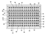
- FIG. 3 is a plan view showing the inside of the backlight shown in FIG.
- FIG. 4 is a plan view showing a plurality of areas that can be individually lit in the backlight.
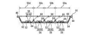
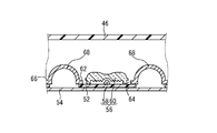
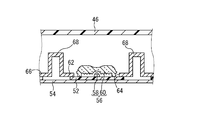
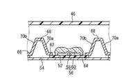
- 5 is a cross-sectional view taken along the line VV in FIG. 6 is a partially enlarged sectional view of FIG.
- FIG. 7 is a graph showing the luminance of the area where the light emitting element group emitting light is located and the other areas, with and without the reflecting wall.
- FIG. 1 is a functional block diagram showing an example of a schematic configuration of a stereoscopic display system as an embodiment of the present invention.
- FIG. 2 is a schematic diagram illustrating an example of a schematic configuration of the stereoscopic display device illustrated in FIG.
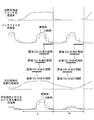
- FIG. 8 is a graph showing light intensity through stereoscopic glasses with and without a reflecting wall.
- FIG. 9 is a plan view showing the inside of the backlight employed in the first application example of the embodiment.
- FIG. 10 is an enlarged cross-sectional view of a reflection wall employed in application example 2 of the embodiment.
- FIG. 11 is an enlarged cross-sectional view of a reflection wall employed in application example 3 of the embodiment.
- FIG. 12 is an enlarged cross-sectional view of a reflection wall employed in application example 4 of the embodiment.
- FIG. 13 is an enlarged cross-sectional view of a reflecting wall employed in Application Example 5 of the embodiment.
- a stereoscopic display system includes a display area in which a plurality of pixels are formed in a matrix, and a right-eye image and a left-eye image are alternately displayed in the display area.
- a liquid crystal panel, stereoscopic glasses whose light transmission state is controlled in synchronization with an image switching period in the liquid crystal panel, and a plurality of glasses arranged behind the liquid crystal panel and arranged in one direction of the display area A backlight that can be sequentially turned on for each section, the backlight is disposed corresponding to each of the plurality of sections, and disposed on a substrate on which the light emitting element group is provided,
- a reflection sheet that reflects light emitted from the light emitting element group; and a reflection wall that is provided on the reflection sheet and on a boundary between the plurality of areas and reflects light emitted from the light emitting element group.
- the luminescent element Emitting elements constituting the group is provided with a point light source, a diffusion lens for diffusing light emitted by the point
- a reflecting wall is provided on the boundary between a plurality of areas. Therefore, the light emitted from the light emitting element group is difficult to leak out of the area where the light emitting element group is disposed. As a result, crosstalk is reduced.
- the point light source refers to a light source that is not a linear light source such as a cold cathode tube or a planar light source such as an organic EL (electroluminescence).
- Examples of the point light source include a light emitting diode and a laser element.
- the second configuration is a configuration in which the reflection wall is integrally formed with the reflection sheet in the first configuration.
- the reflection sheet and the reflection wall can be handled together.
- a reflective wall and a reflective sheet can be manufactured simultaneously.
- the third configuration is a configuration in which, in the first or second configuration, the reflection wall includes a pair of inclined surfaces whose separation distance gradually decreases as the distance from the reflection sheet increases. In such a configuration, light emitted from the light emitting element group is easily reflected by the reflecting wall.
- the fourth configuration is a configuration in which the reflecting wall has a triangular cross section in the third configuration.
- a ridge line is formed at the tip of the reflecting wall. Therefore, it is possible to prevent a portion corresponding to the tip of the reflection wall from appearing bright or dark as compared to the case where a surface is formed at the tip of the reflection wall.
- the fifth configuration is a configuration in which, in any one of the first to fourth configurations, the tip of the reflection wall is located closer to the liquid crystal panel than the diffusion lens. In such a configuration, light emitted from the light emitting element group is easily reflected by the reflecting wall.
- the sixth configuration is a configuration in which the reflection sheet includes an opening for accommodating the light emitting element in any one of the first to fifth configurations. In such a configuration, the area of the reflection sheet increases.
- each figure referred below demonstrates the simplified main component required in order to demonstrate this invention among the structural members of embodiment of this invention for convenience of explanation. Therefore, the three-dimensional display system according to the present invention can include arbitrary constituent members that are not shown in the drawings referred to in this specification. Moreover, the dimension of the member in each figure does not represent the dimension of an actual structural member, the dimension ratio of each member, etc. faithfully.
- FIG. 1 is a functional block diagram illustrating a schematic configuration of the stereoscopic display system 10.
- FIG. 2 is a schematic diagram illustrating a schematic configuration of the stereoscopic display device 12 illustrated in FIG. 1.
- the stereoscopic display system 10 includes a stereoscopic display device 12 and stereoscopic vision glasses 14. Specific examples of the stereoscopic display device 12 include a home television.
- the stereoscopic display device 12 displays a stereoscopic image.
- Stereoscopic images are a right-eye image viewed with the viewer's right eye and a left-eye image viewed with the viewer's left eye.
- the stereoscopic display device 12 includes a liquid crystal panel 16, a backlight 18, and a control unit 20.
- the liquid crystal panel 16 includes an active matrix substrate 22, a counter substrate 24, and a liquid crystal layer 26 sealed between the active matrix substrate 22 and the counter substrate 24.
- the mode of the liquid crystal is not particularly limited.
- the 3D driving method is not particularly limited.
- the liquid crystal panel 16 has a plurality of pixels (not shown).
- the plurality of pixels are formed in a matrix.
- the area where the plurality of pixels are formed is the display area 28 of the liquid crystal panel 16 (see FIG. 1).
- Each pixel may have a plurality of sub-pixels.
- the plurality of sub-pixels are, for example, a red pixel, a green pixel, and a blue pixel.
- the plurality of sub-pixels may include yellow pixels.
- the backlight 18 is a direct type backlight 18.
- the backlight 18 is disposed behind the liquid crystal panel 16 (on the side opposite to the viewer).
- the backlight 18 irradiates the display area 28 with light. Details of the backlight 18 will be described later.
- Control unit 20 drives stereoscopic display device 12. As shown in FIG. 1, the control unit 20 includes a liquid crystal driving unit 30, a backlight driving unit 32, and a glasses driving unit 34.
- the liquid crystal driving unit 30 drives the liquid crystal panel 16.
- the liquid crystal drive unit 30 generates various signals necessary for image display based on a display data signal sent from the outside and a timing control signal. As shown in FIG. 1, the liquid crystal driving unit 30 outputs the generated signal to the gate driver 36 and the source driver 38.
- a plurality of gate lines 40 are connected to the gate driver 36.
- Each gate line 40 is connected to a gate electrode of a thin film transistor (not shown).
- the thin film transistor is formed on the active matrix substrate 22.
- the thin film transistor functions as a switching element.
- Each gate line 40 transmits a scanning signal output from the gate driver 36.
- the thin film transistor is driven by the scanning signal input to the gate electrode.
- a plurality of source lines 42 are connected to the source driver 38. Each source line 42 is connected to the source electrode of the thin film transistor. Each source line 42 transmits a display signal output from the source driver 38.
- a display signal is input to the thin film transistor.
- the storage capacitor is composed of a pixel electrode, a common electrode disposed opposite to the pixel electrode, and a liquid crystal layer 26 positioned between the pixel electrode and the common electrode.
- the pixel electrode is formed on the active matrix substrate 22.
- the pixel electrode is connected to the drain electrode of the thin film transistor.
- the common electrode is formed on the counter substrate 24.
- the backlight drive unit 32 controls the backlight 18. A method for driving the backlight 18 will be described later.
- the glasses driving unit 34 drives the stereoscopic glasses 14.
- the stereoscopic glasses 14 include a right-eye liquid crystal shutter 14a and a left-eye liquid crystal shutter 14b.
- the right-eye liquid crystal shutter 14a is positioned in front of the right eye of the observer in a state where the observer wears the stereoscopic glasses 14.
- the left-eye liquid crystal shutter 14b is positioned in front of the left eye of the observer in a state where the observer wears the stereoscopic glasses 14.
- these liquid crystal shutters 14a and 14b for example, a liquid crystal panel or the like can be employed.
- the glasses driving unit 34 opens and closes the right-eye liquid crystal shutter 14a and the left-eye liquid crystal shutter 14b.
- the right-eye liquid crystal shutter 14a is opened (light transmission state), and the left-eye liquid crystal shutter 14b is closed (light non-transmission state).
- the left-eye liquid crystal shutter 14b is opened (light transmission state), and the right-eye liquid crystal shutter 14a is closed (light non-transmission state).
- FIG. 3 is a plan view showing the inside of the backlight 18.
- FIG. 4 is a plan view showing a plurality of areas that can be individually lit in the backlight 18.
- 5 is a cross-sectional view taken along the line VV in FIG. 6 is a partially enlarged sectional view of FIG. 3 and 4, the left-right direction corresponds to the horizontal direction of the display area 28 (see FIG. 1), and the up-down direction corresponds to the vertical direction of the display area 28.
- the left-right direction corresponds to the vertical direction of the display area 28, the direction perpendicular to the paper surface corresponds to the horizontal direction of the display area 28, and the upper side is the liquid crystal panel 16 side.
- the backlight 18 includes a housing 44 as shown in FIG. As shown in FIG. 5, the housing 44 opens to the liquid crystal panel 16 side. The opening of the housing 44 is covered with an optical sheet 46.
- the optical sheet 46 may be, for example, only a diffusion sheet, or may be a laminate of a plurality of optical sheets including a diffusion sheet.
- a plurality of light emitting element groups 48 are arranged in the housing 44.
- the plurality of light emitting element groups 48 can be turned on for each light emitting element group 48.
- the backlight 18 has a plurality of areas 50a to 50d that can be individually lit as shown in FIGS.
- a plurality of areas 50a to 50d are hatched.
- the display area 28 (see FIG. 1) is substantially divided into a plurality of areas. In other words, areas corresponding to the respective areas 50 a to 50 d are formed in the display area 28.
- the plurality of areas 50a to 50d are arranged in the vertical direction. Therefore, the display area 28 is divided into a plurality of areas in the vertical direction.
- Each area 50a to 50d is turned on by the backlight drive unit 32 (see FIG. 1). Each of the areas 50a to 50d is turned on in response to driving of the liquid crystal panel 16 (see FIG. 1). The plurality of areas 50a to 50d are repeatedly turned on one by one in order from the top.
- each light emitting element group 48 is mounted on one substrate 52.
- a plurality of substrates 52 are accommodated in the housing 44.
- a light emitting element group 48 is mounted on each of the plurality of substrates 52.
- Each substrate 52 extends with a substantially constant width dimension in the horizontal direction.
- the plurality of substrates 52 are arranged at equal intervals in the vertical direction.
- the plurality of substrates 52 overlap the bottom wall 54 of the housing 44.
- Each light emitting element group 48 includes a plurality of light emitting elements 56 as shown in FIG.
- the plurality of light emitting elements 56 are arranged in a line in the horizontal direction.
- the plurality of light emitting elements 56 are arranged at equal intervals.
- Each light emitting element 56 includes a light emitting diode 58 and a diffusing lens 60, as shown in FIG.
- the light emitting diode 58 functions as a point light source.
- the light emitting diode 58 emits white light.
- the diffusion lens 60 covers the light emitting diode 58.
- a gap is formed between the diffusion lens 60 and the light emitting diode 58. By utilizing this gap, the heat of the light emitting diode 58 is released.
- the diffusion lens 60 diffuses the light emitted from the light emitting diode 58. Therefore, each light emitting element 56 can emit uniform light over a wide range.
- a reflection sheet 62 is disposed in the housing 44.
- the reflection sheet 62 overlaps each mounting surface of the plurality of substrates 52.
- the reflection sheet 62 reflects light that has not traveled toward the optical sheet 46 out of the light emitted from each light emitting element 48, and travels toward the optical sheet 46.
- the reflection sheet 62 may be, for example, a foaming reflection plate or a sheet in which a reflection layer is formed on the surface of a resin film.
- the foaming reflection plate includes a bubble in a PET (polyethylene terephthalate) film or a PP (polypropylene) film so as to reflect light itself.
- the sheet in which the reflective layer is formed on the surface of the resin film is, for example, a film in which a reflective layer is formed by sputtering silver on a PET film or PP film.
- the reflection sheet 62 has a plurality of openings 64. Each opening 64 is formed at a position corresponding to the light emitting element 56. When the reflection sheet 62 overlaps each mounting surface of the plurality of substrates 52, one light emitting element 56 is positioned in each opening 64. In such a reflection sheet 62, a large reflection surface 66 of the reflection sheet 62 can be secured.
- the reflection sheet 62 has a plurality of reflection walls 68.
- Each reflecting wall 68 is located on the boundary between two adjacent areas 50a to 50d. In other words, a plurality of areas 50 a to 50 d are defined by the plurality of reflecting walls 68.
- Each reflecting wall 68 reflects the light emitted from each light emitting element 56 toward the other areas 50a to 50d, and transmits the light to the optical sheet 46 in the areas 50a to 50d where the light emitting elements 56 are located. Is incident.
- Each reflection wall 68 is formed by bending the reflection sheet 62 as shown in FIG. That is, each reflection wall 68 is integrally formed with the reflection sheet 62. Thereby, the reflection sheet 62 and the plurality of reflection walls 68 can be handled together. Further, when the reflection sheet 62 is manufactured, a plurality of reflection walls 68 can also be manufactured.
- Each reflection wall 68 has a pair of inclined surfaces 70a and 70b extending in the horizontal direction, as shown in FIG.
- the distance between the pair of inclined surfaces 70 a and 70 b decreases as the distance from the reflection sheet 62 increases.
- a ridgeline 69 is formed by connecting one end (end on the liquid crystal panel 16 side) of the pair of inclined surfaces 70a and 70b. That is, in this embodiment, as shown in FIG. 6, the cross section of each reflecting wall 68 is a triangle.
- one inclined surface 70 a is inclined with respect to the reflecting surface 66 by a predetermined angle ⁇ 1.
- the other inclined surface 70b is inclined with respect to the reflecting surface 66 by a predetermined angle ⁇ 2.
- These angles ⁇ 1 and ⁇ 2 are not particularly limited as long as they are each 90 degrees or more.
- the angle ⁇ 1 and the angle ⁇ 2 may be the same or different.
- each reflecting wall 68 only needs to be located closer to the liquid crystal panel 16 than the upper end of the light emitting diode 58, but as shown in FIG. It is desirable to be located in Thereby, more light can be reflected by the reflecting wall 68.
- a gap is formed between the tip of each reflection wall 68 and the back surface of the optical sheet 46.
- the contact portion can be prevented from appearing dark. Further, at least one of the reflection wall 68 and the optical sheet 46 can be prevented from being damaged, for example.
- Each light emitting element 56 includes a light emitting diode 58 and a diffusing lens 60. Therefore, each light emitting element 56 can emit uniform light over a wide range. In the absence of the plurality of reflecting walls 68, the light emitted from each light emitting element 56 easily reaches the areas 50a to 50d different from the areas 50a to 50d where the light emitting elements 56 are located. In other words, the light emitted from each light emitting element 56 is likely to leak to the other areas 50a to 50d. Therefore, even if the backlight 18 is turned on for each of the areas 50a to 50d, the light of the other areas 50a to 50d leaks to the areas 50a to 50d that are not normally lit. As a result, crosstalk occurs.
- a plurality of reflecting walls 68 are provided. Therefore, the light emitted from each light emitting element 56 is difficult to leak to the other areas 50a to 50d. As a result, crosstalk can be reduced. Further, the light intensity of the areas 50a to 50d where the light emitting element group 48 emitting light is located can be increased.
- each reflection wall 68 has a pair of inclined surfaces 70a and 70b. Therefore, the light emitted from each light emitting element 56 is easily reflected.
- each reflecting wall 68 is a triangle. Therefore, compared to the case where a surface is formed at the tip of the reflecting wall 68, it is possible to prevent the portion corresponding to the tip of the reflecting wall 68 from appearing bright or dark. It is mainly the pair of inclined surfaces 70a and 70b that the reflecting wall 68 reflects light. There is a possibility that light is not reflected at the tip of the reflection wall 68. For this reason, if a surface is formed at the tip of the reflection wall 68, when light is not reflected by the surface, a portion corresponding to the surface appears dark. Conversely, when light is reflected on the surface, the portion corresponding to the surface may appear bright.
- a portion corresponding to the tip of the reflection wall 68 may appear bright or dark.
- the tip of the reflection wall 68 is the ridgeline 69, it is possible to prevent the portion corresponding to the tip of the reflection wall 68 from appearing bright or dark.
- FIG. 7 shows the brightness of the areas 50a to 50d where the light emitting element group 48 emitting light is located, when the reflective wall 68 is provided (Example) and when the reflective wall 68 is not provided (Comparative Example).
- 6 is a graph showing how the brightness of the areas 50a to 50d changes.
- the example is indicated by a solid line
- the comparative example is indicated by a broken line.
- the alternate long and short dash line indicates the position of the ridgeline 69 that each of the two adjacent reflecting walls 68 has.
- the reflection wall 68 when the reflection wall 68 is provided, light leakage to the other areas 50a to 50d can be suppressed as compared with the case where the reflection wall 68 is not provided. Further, the light intensity of the areas 50a to 50d where the light emitting element group 48 emitting light is located can be increased.
- FIG. 8 shows a stereoscopic upper portion of the area corresponding to the area 50b (hereinafter referred to as the corresponding area) in the display area 28 when the plurality of areas 50a to 50d are turned on one by one in order from the top.
- the light intensity when viewed with the glasses 14 is shown.
- FIG. 8 shows a case where the reflecting wall 68 is provided (Example) and a case where the reflecting wall 68 is not provided (Comparative Example).
- FIG. 8 shows the transmittance of the left-eye liquid crystal shutter 14b, the light intensity of the backlight 18, the light emission period of each of the areas 50a to 50d, and the transmittance of the liquid crystal in the corresponding region.
- the switching frequency of the left-eye liquid crystal shutter 14b is 120 Hz.
- Crosstalk is most likely to occur during stereoscopic display when one stereoscopic image is displayed as a white image and the other stereoscopic image is displayed as a black image. Therefore, regarding the transmittance of the liquid crystal, a change in the transmittance of the liquid crystal when the image for the left eye is displayed as a white image and the image for the right eye is displayed as a black image is shown.
- the backlight 18 lights the areas 50a to 50d in accordance with the driving timing of the liquid crystal in the areas corresponding to the areas 50a to 50d to be lit in the display area 28.
- L indicates the display period of the left eye image
- R indicates the display period of the right eye image.
- the brightness of the area 50b is improved in the example as compared with the comparative example.
- the embodiment has less leakage light from the other areas 50a, 50c, and 50d than the comparative example.
- the leakage light from the other areas 50c and 50d enters the area 50b after driving of the liquid crystal in the corresponding area is completed, that is, after the transmittance of the liquid crystal starts to decrease.
- the light utilization efficiency deteriorates.
- the embodiment since the leakage light from the other areas 50c and 50d entering the area 50b after the driving of the liquid crystal in the corresponding area is completed, the light use efficiency is improved.
- the lighting period of the area 50b ends in accordance with the timing when the transmittance of the liquid crystal in the corresponding region is lowest. Therefore, in the comparative example, when the transmittance of the liquid crystal in the corresponding region starts to increase, the leaked light from the other areas 50c and 50d enters the area 50b. Therefore, in the comparative example, the crosstalk value becomes high. On the other hand, in the embodiment, since the leakage light from the other areas 50c and 50d is difficult to enter the area 50b, the crosstalk value becomes low.
- FIG. 9 is a plan view showing the inside of the backlight 18 employed in the first application example.
- FIG. 10 is an enlarged cross-sectional view of the reflecting wall 68 employed in the application example 2.
- FIG. 11 is an enlarged cross-sectional view of the reflecting wall 68 employed in the application example 3.
- FIG. 12 is an enlarged cross-sectional view of the reflecting wall 68 employed in the application example 4.
- FIG. 13 is an enlarged cross-sectional view of the reflecting wall 68 employed in the application example 5.
- the plurality of light emitting elements 56 constituting the light emitting element group 48 need not be arranged in a line.
- a plurality of light emitting elements 56 may be arranged in two rows.
- the cross section of the reflecting wall 68 is not limited to a triangle.
- it may be semi-circular as shown in FIG. 10, rectangular as shown in FIG. 11, or trapezoid as shown in FIG.
- the reflection wall 68 does not need to be integrally formed with the reflection sheet 62.
- the reflection wall 68 may be formed separately from the reflection sheet 62. In this case, the reflection wall 68 is bonded to the reflection sheet 62.
- the reflecting wall 68 may have a hollow structure.
- each light emitting element group 48 is provided on one substrate 52, but a plurality of light emitting element groups 48 may be mounted together on one substrate.
Landscapes
- Physics & Mathematics (AREA)
- General Physics & Mathematics (AREA)
- Nonlinear Science (AREA)
- Engineering & Computer Science (AREA)
- Optics & Photonics (AREA)
- Mathematical Physics (AREA)
- Chemical & Material Sciences (AREA)
- Crystallography & Structural Chemistry (AREA)
- Theoretical Computer Science (AREA)
- Computer Hardware Design (AREA)
- Liquid Crystal (AREA)
- Planar Illumination Modules (AREA)
- Testing, Inspecting, Measuring Of Stereoscopic Televisions And Televisions (AREA)
- Control Of Indicators Other Than Cathode Ray Tubes (AREA)
Abstract
クロストークを軽減することができる立体表示システムを提供することを、目的とする。バックライト(18)は、表示領域(28)の一方向に並ぶ複数の区域(50a~50d)毎に順次点灯可能となっている。バックライト(18)は、発光素子群(48)と、反射シート(62)と、反射壁(68)とを備える。発光素子群(48)は、複数の区域(50a~50d)のそれぞれに対応して配置される。反射シート(62)は、発光素子群(48)が設けられた基板(52)上に配置され、発光素子群(48)が発する光を反射する。反射壁(68)は、反射シート(62)上であって、且つ、複数の区域(50a~50d)の境界上に設けられ、発光素子群(48)が発する光を反射する。発光素子群(48)を構成する発光素子(56)は、点光源(58)と、拡散レンズ(60)とを備える。拡散レンズ(60)は、点光源(58)が発する光を拡散する。
Description
本発明は、立体表示システムに関する。
液晶シャッターメガネを用いて、観察者に立体画像を見せる立体表示装置が知られている。このような立体表示装置は、右眼用画像と左眼用画像を液晶パネルに交互に表示する。画像の切替周期と同期して、液晶シャッターメガネにおける光の透過状態を制御する。これにより、観察者の右眼には右眼用画像だけが見え、左眼には左眼用画像だけが見える。その結果、観察者は、立体感を感じることができる。
立体表示装置においては、右眼用画像と左眼用画像を分離する必要がある。右眼用画像と左眼用画像が分離されていないと、クロストークが発生する。クロストークを軽減する方法としては、例えば、液晶の応答に合わせて、バックライトを画面上の区域毎に点灯する方法がある(シャープ技報第102号第4頁~第7頁参照)。
バックライトは、例えば、特開2009-117207号公報に開示されている。上記公報に記載のバックライトは、発光素子からの光を光束制御部材を介して出射する発光装置を備える。発光装置は、光束制御部材の光制御出射面から効率的に且つ広範囲に均一な照射光を出射する。
上記公報に記載のバックライトは光の広がりが大きい。そのため、上記公報に記載のバックライトを採用し、液晶の応答に合わせて、バックライトを画面上の区域毎に点灯する場合、本来なら点灯していない区域に、光が漏れる。その結果、クロストークが発生する。
本発明の目的は、クロストークを軽減することができる立体表示システムを提供することである。
本発明の立体表示システムは、複数の画素がマトリクス状に形成された表示領域を有し、右眼用画像と左眼用画像とが前記表示領域に交互に切替表示される液晶パネルと、前記液晶パネルにおける画像の切替周期と同期して、光の透過状態が制御される立体視用メガネと、前記液晶パネルの後方に配置され、前記表示領域の一方向に並ぶ複数の区域毎に順次点灯可能なバックライトとを備え、前記バックライトは、前記複数の区域のそれぞれに対応して配置される発光素子群と、前記発光素子群が設けられた基板上に配置され、前記発光素子群が発する光を反射する反射シートと、前記反射シート上であって、且つ、前記複数の区域の境界上に設けられ、前記発光素子群が発する光を反射する反射壁とを備え、前記発光素子群を構成する発光素子は、点光源と、点光源が発する光を拡散する拡散レンズとを備える。
本発明の立体表示システムは、クロストークを軽減することができる。
本発明の一実施形態に係る立体表示システムは、複数の画素がマトリクス状に形成された表示領域を有し、右眼用画像と左眼用画像とが前記表示領域に交互に切替表示される液晶パネルと、前記液晶パネルにおける画像の切替周期と同期して、光の透過状態が制御される立体視用メガネと、前記液晶パネルの後方に配置され、前記表示領域の一方向に並ぶ複数の区域毎に順次点灯可能なバックライトとを備え、前記バックライトは、前記複数の区域のそれぞれに対応して配置される発光素子群と、前記発光素子群が設けられた基板上に配置され、前記発光素子群が発する光を反射する反射シートと、前記反射シート上であって、且つ、前記複数の区域の境界上に設けられ、前記発光素子群が発する光を反射する反射壁とを備え、前記発光素子群を構成する発光素子は、点光源と、点光源が発する光を拡散する拡散レンズとを備える(第1の構成)。
第1の構成においては、複数の区域の境界上に反射壁が設けられている。そのため、発光素子群が発する光は、当該発光素子群が配置された区域の外へ漏れ難くなる。その結果、クロストークが軽減される。
なお、点光源は、冷陰極管等の線状光源や、有機EL(electroluminescence)等の面状光源ではない光源をいう。点光源としては、例えば、発光ダイオード、レーザー素子等がある。
第2の構成は、前記第1の構成において、前記反射壁が前記反射シートに一体形成されている構成である。このような構成においては、反射シートと反射壁を纏めて取り扱うことができる。また、反射壁と反射シートを同時に製造することができる。
第3の構成は、前記第1又は第2の構成において、前記反射壁は、前記反射シートから離れるに従って次第に離隔距離が短くなる一対の傾斜面を備える構成である。このような構成においては、発光素子群の発する光が反射壁によって反射され易くなる。
第4の構成は、前記第3の構成において、前記反射壁の断面が三角形になっている構成である。このような構成においては、反射壁の先端に稜線が形成される。そのため、反射壁の先端に面が形成される場合に比して、反射壁の先端に相当する部分が明るく見えたり、暗く見えたりするのを防ぐことができる。
第5の構成は、前記第1~第4の構成の何れか1つにおいて、前記反射壁の先端が前記拡散レンズよりも前記液晶パネル側に位置している構成である。このような構成においては、発光素子群の発する光が反射壁で反射され易くなる。
第6の構成は、前記第1~第5の構成の何れか1つにおいて、前記反射シートは、前記発光素子を収容する開口を備える構成である。このような構成においては、反射シートの面積が大きくなる。
以下、本発明のより具体的な実施形態について、図面を参照しながら説明する。なお、以下で参照する各図は、説明の便宜上、本発明の実施形態の構成部材のうち、本発明を説明するために必要な主要部材のみを簡略化して示したものである。従って、本発明に係る立体表示システムは、本明細書が参照する各図に示されていない任意の構成部材を備え得る。また、各図中の部材の寸法は、実際の構成部材の寸法および各部材の寸法比率等を忠実に表したものではない。
[実施形態]
図1及び図2を参照して、本発明の第1の実施形態としての立体表示システム10について説明する。図1は、立体表示システム10の概略構成を示す機能ブロック図である。図2は、図1に示す立体表示装置12の概略構成を示す模式図である。
図1及び図2を参照して、本発明の第1の実施形態としての立体表示システム10について説明する。図1は、立体表示システム10の概略構成を示す機能ブロック図である。図2は、図1に示す立体表示装置12の概略構成を示す模式図である。
[全体構成]
立体表示システム10は、立体表示装置12と、立体視用メガネ14とを備える。立体表示装置12の具体例としては、例えば、家庭用テレビ等がある。
立体表示システム10は、立体表示装置12と、立体視用メガネ14とを備える。立体表示装置12の具体例としては、例えば、家庭用テレビ等がある。
立体表示装置12は、立体視用画像を表示する。立体視用画像は、観察者の右眼で見る右眼用画像と、観察者の左眼で見る左眼用画像とである。立体表示装置12は、液晶パネル16と、バックライト18と、制御部20とを備える。
図2に示すように、液晶パネル16は、アクティブマトリクス基板22と、対向基板24と、これらアクティブマトリクス基板22と対向基板24との間に封入された液晶層26とを備える。液晶のモードは、特に限定されない。3Dの駆動方式も、特に限定されない。
液晶パネル16は、複数の画素(図示せず)を有する。複数の画素は、マトリクス状に形成されている。複数の画素が形成された領域は、液晶パネル16の表示領域28(図1参照)である。
各画素は、複数のサブ画素を有してもよい。複数のサブ画素は、例えば、赤色画素、緑色画素及び青色画素である。複数のサブ画素は、黄色画素を含んでもよい。
バックライト18は、直下型のバックライト18である。バックライト18は、液晶パネル16の後方(観察者とは反対側)に配置される。バックライト18は、表示領域28に光を照射する。バックライト18の詳細については、後述する。
制御部20(図1参照)は、立体表示装置12を駆動する。制御部20は、図1に示すように、液晶駆動部30と、バックライト駆動部32と、メガネ駆動部34とを備える。
液晶駆動部30は、液晶パネル16を駆動する。液晶駆動部30は、外部から送られてくる表示データ信号と、タイミング制御信号とに基づいて、画像表示に必要な各種信号を生成する。図1に示すように、液晶駆動部30は、ゲートドライバ36とソースドライバ38に対して、生成した信号を出力する。
ゲートドライバ36には、複数のゲート線40が接続されている。各ゲート線40は、薄膜トランジスタ(図示せず)のゲート電極に接続されている。薄膜トランジスタは、アクティブマトリクス基板22上に形成されている。薄膜トランジスタは、スイッチング素子として機能する。各ゲート線40は、ゲートドライバ36から出力される走査信号を伝送する。ゲート電極に入力される走査信号によって、薄膜トランジスタが駆動される。
ソースドライバ38には、複数のソース線42が接続されている。各ソース線42は、薄膜トランジスタのソース電極に接続されている。各ソース線42は、ソースドライバ38から出力される表示信号を伝送する。薄膜トランジスタが駆動されているときに、薄膜トランジスタに表示信号が入力される。これにより、表示信号に応じた電荷が、薄膜トランジスタに接続された蓄積容量に蓄積される。蓄積容量は、画素電極と、画素電極に対向して配置された共通電極と、これら画素電極と共通電極との間に位置する液晶層26とによって構成される。画素電極は、アクティブマトリクス基板22に形成されている。画素電極は、薄膜トランジスタのドレイン電極に接続されている。共通電極は、対向基板24に形成されている。表示信号に応じた電荷を蓄積容量に蓄積することにより、各画素の階調を制御することができる。その結果、液晶パネル16は、画像を表示することができる。
バックライト駆動部32は、バックライト18を制御する。バックライト18の駆動方法については、後述する。
メガネ駆動部34は、立体視用メガネ14を駆動する。立体視用メガネ14は、右眼用液晶シャッタ14aと、左眼用液晶シャッタ14bとを備える。右眼用液晶シャッタ14aは、観察者が立体視用メガネ14を装着した状態で、観察者の右眼前方に位置する。左眼用液晶シャッタ14bは、観察者が立体視用メガネ14を装着した状態で、観察者の左眼前方に位置する。これらの液晶シャッタ14a,14bとしては、例えば、液晶パネル等を採用することができる。
メガネ駆動部34は、右眼用液晶シャッタ14aと左眼用液晶シャッタ14bを開閉する。液晶パネル16が右眼用画像を表示するとき、右眼用液晶シャッタ14aを開状態(光の透過状態)とし、左眼用液晶シャッタ14bを閉状態(光の非透過状態)とする。液晶パネル16が左眼用画像を表示するとき、左眼用液晶シャッタ14bを開状態(光の透過状態)とし、右眼用液晶シャッタ14aを閉状態(光の非透過状態)とする。
[バックライト]
次に、図3~図6を参照して、バックライト18の詳細について説明する。図3は、バックライト18の内部を示す平面図である。図4は、バックライト18において個別に点灯可能な複数の区域を示す平面図である。図5は、図4におけるV-V断面図である。図6は、図5の一部拡大断面図である。なお、図3及び図4においては、左右方向が表示領域28(図1参照)の水平方向に対応し、上下方向が表示領域28の垂直方向に対応する。図5及び図6においては、左右方向が表示領域28の垂直方向に対応し、紙面に垂直な方向が表示領域28の水平方向に対応し、上側が液晶パネル16側になる。
次に、図3~図6を参照して、バックライト18の詳細について説明する。図3は、バックライト18の内部を示す平面図である。図4は、バックライト18において個別に点灯可能な複数の区域を示す平面図である。図5は、図4におけるV-V断面図である。図6は、図5の一部拡大断面図である。なお、図3及び図4においては、左右方向が表示領域28(図1参照)の水平方向に対応し、上下方向が表示領域28の垂直方向に対応する。図5及び図6においては、左右方向が表示領域28の垂直方向に対応し、紙面に垂直な方向が表示領域28の水平方向に対応し、上側が液晶パネル16側になる。
バックライト18は、図5に示すように、ハウジング44を備える。図5に示すように、ハウジング44は、液晶パネル16側に開口する。ハウジング44の開口は、光学シート46で覆われている。光学シート46は、例えば、拡散シートだけであってもよいし、拡散シートを含む複数の光学シートが積層されたものであってもよい。
図3に示すように、ハウジング44内には、複数の発光素子群48が配置されている。複数の発光素子群48は、発光素子群48ごとに点灯可能となっている。これにより、バックライト18は、図4及び図5に示すように、個別に点灯可能な複数の区域50a~50dを有する。なお、図4においては、複数の区域50a~50dにハッチングを施している。
バックライト18が複数の区域50a~50dを有することに伴い、表示領域28(図1参照)が実質的に複数の領域に分けられる。換言すれば、各区域50a~50dに対応する領域が、表示領域28に形成される。
複数の区域50a~50dは、垂直方向に並んでいる。そのため、表示領域28は、垂直方向に複数の領域に分けられる。
各区域50a~50dは、バックライト駆動部32(図1参照)によって、点灯される。各区域50a~50dは、液晶パネル16(図1参照)の駆動に対応して、点灯される。複数の区域50a~50dは、上から順番に1つずつ繰り返し点灯される。
図3に示すように、各発光素子群48は、1つの基板52に実装されている。換言すれば、ハウジング44内には、複数の基板52が収容されている。これら複数の基板52のそれぞれに発光素子群48が実装されている。
各基板52は、水平方向に略一定の幅寸法で延びている。複数の基板52は、垂直方向に等間隔に並んでいる。複数の基板52は、ハウジング44の底壁54に重なっている。
各発光素子群48は、図3に示すように、複数の発光素子56を含んで構成されている。複数の発光素子56は、水平方向に1列に並んでいる。複数の発光素子56は、等間隔に配置されている。
各発光素子56は、図5に示すように、発光ダイオード58と、拡散レンズ60とを備える。本実施形態では、発光ダイオード58が点光源として機能する。
発光ダイオード58は、白色光を発する。拡散レンズ60は、発光ダイオード58を覆っている。
拡散レンズ60と発光ダイオード58との間には、隙間が形成されている。この隙間を利用して、発光ダイオード58の熱を逃がす。
拡散レンズ60は、発光ダイオード58が発する光を拡散する。そのため、各発光素子56は、広範囲に均一な光を出射することができる。
図5に示すように、ハウジング44内には、反射シート62が配置されている。反射シート62は、複数の基板52のそれぞれの実装面に重なっている。反射シート62は、各発光素子48から発せられた光のうち、光学シート46に向かって進まなかった光を反射し、光学シート46に向かって進ませる。反射シート62は、例えば、発砲反射板であってもよいし、樹脂フィルムの表面に反射層を形成したシートであってもよい。発砲反射板は、例えば、PET(ポリエチレンテレフタレート)フィルムやPP(ポリプロピレン)フィルムに気泡を含ませることにより、それ自身が光を反射する特性を有するようにしたものである。樹脂フィルムの表面に反射層を形成したシートは、例えば、PETフィルムやPPフィルムに銀をスパッタして反射層を形成したものである。
図3及び図5に示すように、反射シート62は、複数の開口64を有する。各開口64は、発光素子56と対応する位置に形成されている。反射シート62が複数の基板52のそれぞれの実装面に重なっているとき、各開口64内には、1つの発光素子56が位置している。このような反射シート62においては、反射シート62の反射面66を大きく確保することができる。
[反射壁]
反射シート62は、図3及び図5に示すように、複数の反射壁68を有する。各反射壁68は、隣り合う2つの区域50a~50dの境界上に位置する。換言すれば、複数の反射壁68によって、複数の区域50a~50dが規定されている。
反射シート62は、図3及び図5に示すように、複数の反射壁68を有する。各反射壁68は、隣り合う2つの区域50a~50dの境界上に位置する。換言すれば、複数の反射壁68によって、複数の区域50a~50dが規定されている。
各反射壁68は、各発光素子56から発せられた光のうち、他の区域50a~50dに向かう光を反射し、当該発光素子56が位置する区域50a~50d内で、光学シート46に光を入射させる。
各反射壁68は、図5に示すように、反射シート62を折り曲げることで形成されている。即ち、各反射壁68は、反射シート62に一体形成されている。これにより、反射シート62と複数の反射壁68とを纏めて取り扱うことができる。また、反射シート62を製造するときに、複数の反射壁68も製造することができる。
各反射壁68は、図6に示すように、水平方向に延びる一対の傾斜面70a,70bを有する。一対の傾斜面70a,70bは、反射シート62から離れるに従って離隔距離が短くなっている。一対の傾斜面70a,70bの一端(液晶パネル16側の端)同士が繋がることで、稜線69が形成されている。即ち、本実施形態では、図6に示すように、各反射壁68の断面が三角形になっている。
図6に示すように、一方の傾斜面70aは、反射面66に対して、所定角度θ1傾斜している。他方の傾斜面70bは、反射面66に対して、所定角度θ2傾斜している。これらの角度θ1,θ2は、それぞれ、90度以上であれば、特に限定されない。角度θ1と角度θ2は、同じであってもよいし、異なっていてもよい。
各反射壁68の先端(稜線69)は、発光ダイオード58の上端よりも液晶パネル16側に位置していればよいが、図6に示すように、拡散レンズ60の上端よりも液晶パネル16側に位置するほうが望ましい。これにより、より多くの光を反射壁68で反射することができる。
なお、図6に示すように、各反射壁68の先端と光学シート46の裏面との間に隙間が形成されていることが好ましい。反射壁68が光学シート46に接触した場合、当該接触部分が暗く見えるのを防ぐことができる。また、反射壁68と光学シート46の少なくとも一方が、例えば破損等するのを防ぐことができる。
[実施形態の効果]
各発光素子56は、発光ダイオード58と、拡散レンズ60とを備える。そのため、各発光素子56は、広範囲に均一な光を出射することができる。複数の反射壁68がない場合、各発光素子56が発する光は、当該発光素子56が位置する区域50a~50dとは異なる区域50a~50dにまで容易に到達する。換言すれば、各発光素子56の発する光が他の区域50a~50dに漏れ易くなっている。そのため、バックライト18を区域50a~50d毎に点灯しても、本来なら点灯していない区域50a~50dに、他の区域50a~50dの光が漏れてしまう。その結果、クロストークが発生する。
各発光素子56は、発光ダイオード58と、拡散レンズ60とを備える。そのため、各発光素子56は、広範囲に均一な光を出射することができる。複数の反射壁68がない場合、各発光素子56が発する光は、当該発光素子56が位置する区域50a~50dとは異なる区域50a~50dにまで容易に到達する。換言すれば、各発光素子56の発する光が他の区域50a~50dに漏れ易くなっている。そのため、バックライト18を区域50a~50d毎に点灯しても、本来なら点灯していない区域50a~50dに、他の区域50a~50dの光が漏れてしまう。その結果、クロストークが発生する。
しかしながら、本実施形態においては、複数の反射壁68が設けられている。そのため、各発光素子56の発する光が他の区域50a~50dに漏れ難くなっている。その結果、クロストークを軽減することができる。また、光を発する発光素子群48が位置する区域50a~50dの光強度を大きくすることができる。
本実施形態では、各反射壁68が一対の傾斜面70a,70bを有する。そのため、各発光素子56の発する光を反射し易くなっている。
特に本実施形態では、各反射壁68の断面が三角形となっている。そのため、反射壁68の先端に面が形成されている場合に比して、反射壁68の先端に相当する部分が明るく見えたり、暗く見えたりするのを防ぐことができる。反射壁68が光を反射するのは、主に、一対の傾斜面70a,70bである。反射壁68の先端では、光を反射しない可能性がある。そのため、反射壁68の先端に面が形成されていると、当該面で光を反射しなかった場合、当該面に相当する部分が暗く見える。逆に、当該面で光を反射した場合、当該面に相当する部分が明るく見える可能性がある。このように、反射壁68の先端に面が形成されている場合、反射壁68の先端に相当する部分が明るく見えたり、暗く見えたりする可能性がある。しかしながら、本実施形態では、反射壁68の先端が稜線69になっているので、反射壁68の先端に相当する部分が明るく見えたり、暗く見えたりするのを防ぐことができる。
図7は、反射壁68を有する場合(実施例)と、反射壁68を有しない場合(比較例)とで、光を発する発光素子群48が位置する区域50a~50dの輝度と、他の区域50a~50dの輝度とが、どのように変化するかを示すグラフである。図7においては、実施例を実線で示し、比較例を破線で示す。なお、図7において、一点鎖線は、隣り合う2つの反射壁68のそれぞれが有する稜線69の位置を示す。
図7に示すように、反射壁68を有する場合は、反射壁68を有しない場合に比して、他の区域50a~50dへの光の漏れを抑えることができる。また、光を発する発光素子群48が位置する区域50a~50dの光強度を大きくすることができる。
図8は、複数の区域50a~50dを上から順番に1つずつ点灯したときに、表示領域28において区域50bに対応する領域(以下、対応領域とする)の中央上側部分を、立体視用メガネ14をかけて見た場合の光強度を示す。図8には、反射壁68を有する場合(実施例)と、反射壁68を有しない場合(比較例)とが示されている。図8には、左眼用液晶シャッタ14bの透過率と、バックライト18の光強度と、各区域50a~50dの発光期間と、対応領域の液晶の透過率とが、併せて示されている。左眼用液晶シャッタ14bの切替周波数は、120Hzである。立体表示の際にクロストークが最も発生し易いのは、一方の立体視用画像を白画像で表示し、他方の立体視用画像を黒画像で表示する場合である。そこで、液晶の透過率については、左眼用画像を白画像で表示し、右眼用画像を黒画像で表示したときの液晶の透過率の変化を示す。バックライト18は、表示領域28において点灯する区域50a~50dに対応する領域の液晶の駆動タイミングに合わせて、各区域50a~50dを点灯している。図中、Lは左眼用画像の表示期間を示し、Rは右眼用画像の表示期間を示す。
[白画像の表示期間]
図8に示すように、実施例は、比較例よりも、区域50bの輝度が向上している。実施例は、比較例よりも、他の区域50a,50c,50dからの漏れ光が少ない。比較例においては、他の区域50c,50dからの漏れ光は、対応領域の液晶の駆動が終了した後、即ち、液晶の透過率が下がり始めた後に、区域50bに入ってくる。そのため、光の利用効率が悪くなる。一方、実施例においては、対応領域の液晶の駆動が終了した後に区域50bに入ってくる他の区域50c,50dからの漏れ光が少ないので、光の利用効率がよくなる。
図8に示すように、実施例は、比較例よりも、区域50bの輝度が向上している。実施例は、比較例よりも、他の区域50a,50c,50dからの漏れ光が少ない。比較例においては、他の区域50c,50dからの漏れ光は、対応領域の液晶の駆動が終了した後、即ち、液晶の透過率が下がり始めた後に、区域50bに入ってくる。そのため、光の利用効率が悪くなる。一方、実施例においては、対応領域の液晶の駆動が終了した後に区域50bに入ってくる他の区域50c,50dからの漏れ光が少ないので、光の利用効率がよくなる。
[黒画像の表示期間]
図8に示すように、区域50bの点灯期間は、対応領域の液晶の透過率が最も低くなるタイミングに合わせて、終了するようになっている。そのため、比較例では、対応領域の液晶の透過率が上がり始めるときに、他の区域50c,50dからの漏れ光が区域50bに入り込んでくる。そのため、比較例では、クロストーク値が高くなる。一方、実施例では、他の区域50c,50dからの漏れ光が区域50bに入り込み難くなっているので、クロストーク値が低くなる。
図8に示すように、区域50bの点灯期間は、対応領域の液晶の透過率が最も低くなるタイミングに合わせて、終了するようになっている。そのため、比較例では、対応領域の液晶の透過率が上がり始めるときに、他の区域50c,50dからの漏れ光が区域50bに入り込んでくる。そのため、比較例では、クロストーク値が高くなる。一方、実施例では、他の区域50c,50dからの漏れ光が区域50bに入り込み難くなっているので、クロストーク値が低くなる。
[実施形態の応用例1~5]
図9~図13を参照して、実施形態の応用例1~5について説明する。図9は、応用例1で採用されるバックライト18の内部を示す平面図である。図10は、応用例2で採用される反射壁68の拡大断面図である。図11は、応用例3で採用される反射壁68の拡大断面図である。図12は、応用例4で採用される反射壁68の拡大断面図である。図13は、応用例5で採用される反射壁68の拡大断面図である。
図9~図13を参照して、実施形態の応用例1~5について説明する。図9は、応用例1で採用されるバックライト18の内部を示す平面図である。図10は、応用例2で採用される反射壁68の拡大断面図である。図11は、応用例3で採用される反射壁68の拡大断面図である。図12は、応用例4で採用される反射壁68の拡大断面図である。図13は、応用例5で採用される反射壁68の拡大断面図である。
発光素子群48を構成する複数の発光素子56は、1列に並んでいる必要はない。例えば、図9に示すように、複数の発光素子56が2列に並んでいてもよい。
反射壁68の断面は、三角形に限定されない。例えば、図10に示すように、半円形であってもよいし、図11に示すように、矩形であってもよいし、図12に示すように、台形であってもよい。
反射壁68は反射シート62に一体形成されている必要はない。例えば、図13に示すように、反射壁68は、反射シート62と別体形成されていてもよい。この場合、反射壁68は、反射シート62に接着される。なお、図13において、反射壁68は中空構造であってもよい。
以上、本発明の実施形態について、詳述してきたが、これらはあくまでも例示であって、本発明は、上述の実施形態によって、何等、限定されない。
例えば、前記実施形態では、各発光素子群48が1つの基板52に設けられていたが、複数の発光素子群48を1つの基板に纏めて実装してもよい。
Claims (6)
- 複数の画素がマトリクス状に形成された表示領域を有し、右眼用画像と左眼用画像とが前記表示領域に交互に切替表示される液晶パネルと、
前記液晶パネルにおける画像の切替周期と同期して、光の透過状態が制御される立体視用メガネと、
前記液晶パネルの後方に配置され、前記表示領域の一方向に並ぶ複数の区域毎に順次点灯可能なバックライトとを備え、
前記バックライトは、
前記複数の区域のそれぞれに対応して配置される発光素子群と、
前記発光素子群が設けられた基板上に配置され、前記発光素子群が発する光を反射する反射シートと、
前記反射シート上であって、且つ、前記複数の区域の境界上に設けられ、前記発光素子群が発する光を反射する反射壁とを備え、
前記発光素子群を構成する発光素子は、
点光源と、
点光源が発する光を拡散する拡散レンズとを備える、立体表示システム。 - 前記反射壁が前記反射シートに一体形成されている、請求項1に記載の立体表示システム。
- 前記反射壁は、前記反射シートから離れるに従って次第に離隔距離が短くなる一対の傾斜面を備える、請求項1又は2に記載の立体表示システム。
- 前記反射壁の断面が三角形である、請求項3に記載の立体表示システム。
- 前記反射壁の先端が前記拡散レンズよりも前記液晶パネル側に位置している、請求項1~4の何れか1項に記載の立体表示システム。
- 前記反射シートは、前記発光素子を収容する開口を備える、請求項1~5の何れか1項に記載の立体表示システム。
Applications Claiming Priority (2)
| Application Number | Priority Date | Filing Date | Title |
|---|---|---|---|
| JP2011140200A JP2014167495A (ja) | 2011-06-24 | 2011-06-24 | 立体表示システム |
| JP2011-140200 | 2011-06-24 |
Publications (1)
| Publication Number | Publication Date |
|---|---|
| WO2012176710A1 true WO2012176710A1 (ja) | 2012-12-27 |
Family
ID=47422548
Family Applications (1)
| Application Number | Title | Priority Date | Filing Date |
|---|---|---|---|
| PCT/JP2012/065378 Ceased WO2012176710A1 (ja) | 2011-06-24 | 2012-06-15 | 立体表示システム |
Country Status (2)
| Country | Link |
|---|---|
| JP (1) | JP2014167495A (ja) |
| WO (1) | WO2012176710A1 (ja) |
Cited By (5)
| Publication number | Priority date | Publication date | Assignee | Title |
|---|---|---|---|---|
| WO2016184111A1 (zh) * | 2015-05-21 | 2016-11-24 | 瑞仪光电(苏州)有限公司 | 反射组件、背光模组和具有该背光模组的显示设备 |
| CN110646983A (zh) * | 2019-10-09 | 2020-01-03 | 深圳市隆利科技股份有限公司 | 面光源的背光装置及显示设备 |
| CN113093433A (zh) * | 2021-04-25 | 2021-07-09 | 业成科技(成都)有限公司 | 光源组件及其制备方法、背光模组和显示装置 |
| CN114779526A (zh) * | 2022-04-14 | 2022-07-22 | 深圳创维-Rgb电子有限公司 | 发光组件、背光模组及显示装置 |
| EP4464935A1 (en) * | 2023-05-17 | 2024-11-20 | Signify Holding B.V. | A luminaire with a flexible sheet |
Families Citing this family (2)
| Publication number | Priority date | Publication date | Assignee | Title |
|---|---|---|---|---|
| JP6414485B2 (ja) | 2015-02-27 | 2018-10-31 | 日亜化学工業株式会社 | 発光装置 |
| JP7760141B2 (ja) * | 2021-02-24 | 2025-10-27 | Wota株式会社 | Uv殺菌装置 |
Citations (3)
| Publication number | Priority date | Publication date | Assignee | Title |
|---|---|---|---|---|
| JP2010175797A (ja) * | 2009-01-29 | 2010-08-12 | Sony Corp | 液晶表示装置組立体、及び、液晶表示装置組立体の駆動方法 |
| WO2011055565A1 (ja) * | 2009-11-06 | 2011-05-12 | シャープ株式会社 | 照明装置、表示装置、及びテレビジョン受像器 |
| JP2011112745A (ja) * | 2009-11-25 | 2011-06-09 | Panasonic Corp | 立体表示装置および立体表示方法 |
-
2011
- 2011-06-24 JP JP2011140200A patent/JP2014167495A/ja not_active Withdrawn
-
2012
- 2012-06-15 WO PCT/JP2012/065378 patent/WO2012176710A1/ja not_active Ceased
Patent Citations (3)
| Publication number | Priority date | Publication date | Assignee | Title |
|---|---|---|---|---|
| JP2010175797A (ja) * | 2009-01-29 | 2010-08-12 | Sony Corp | 液晶表示装置組立体、及び、液晶表示装置組立体の駆動方法 |
| WO2011055565A1 (ja) * | 2009-11-06 | 2011-05-12 | シャープ株式会社 | 照明装置、表示装置、及びテレビジョン受像器 |
| JP2011112745A (ja) * | 2009-11-25 | 2011-06-09 | Panasonic Corp | 立体表示装置および立体表示方法 |
Cited By (5)
| Publication number | Priority date | Publication date | Assignee | Title |
|---|---|---|---|---|
| WO2016184111A1 (zh) * | 2015-05-21 | 2016-11-24 | 瑞仪光电(苏州)有限公司 | 反射组件、背光模组和具有该背光模组的显示设备 |
| CN110646983A (zh) * | 2019-10-09 | 2020-01-03 | 深圳市隆利科技股份有限公司 | 面光源的背光装置及显示设备 |
| CN113093433A (zh) * | 2021-04-25 | 2021-07-09 | 业成科技(成都)有限公司 | 光源组件及其制备方法、背光模组和显示装置 |
| CN114779526A (zh) * | 2022-04-14 | 2022-07-22 | 深圳创维-Rgb电子有限公司 | 发光组件、背光模组及显示装置 |
| EP4464935A1 (en) * | 2023-05-17 | 2024-11-20 | Signify Holding B.V. | A luminaire with a flexible sheet |
Also Published As
| Publication number | Publication date |
|---|---|
| JP2014167495A (ja) | 2014-09-11 |
Similar Documents
| Publication | Publication Date | Title |
|---|---|---|
| US9087470B2 (en) | 3D image display apparatus and driving method thereof | |
| JP5168323B2 (ja) | 表示装置の駆動方法 | |
| CN202206503U (zh) | 立体显示设备和显示驱动电路 | |
| JP4655465B2 (ja) | 面光源及び液晶表示装置 | |
| JP4225132B2 (ja) | 液晶表示装置 | |
| WO2012176710A1 (ja) | 立体表示システム | |
| TWI608253B (zh) | 自動立體顯示裝置及其驅動方法 | |
| JP5436050B2 (ja) | 立体映像表示装置 | |
| KR20080074757A (ko) | 지향성 표시 디스플레이 | |
| US20120306861A1 (en) | Light source device and display | |
| CN103384338A (zh) | 显示单元和电子设备 | |
| JP2012103400A (ja) | 立体表示装置および立体表示装置の表示方法 | |
| KR20140089523A (ko) | 표시 장치 및 전자 기기 | |
| EP1477840A1 (en) | Display unit | |
| JP4608947B2 (ja) | 液晶表示装置 | |
| JP5131331B2 (ja) | 液晶表示装置 | |
| JP2005003989A (ja) | 画像表示装置 | |
| US9548013B2 (en) | Image display device and drive method therefor | |
| TWI689758B (zh) | 具有方向性控制輸出之顯示裝置,及該顯示裝置的背光 | |
| JP2012009154A (ja) | 照明装置および表示装置 | |
| JP2012150366A (ja) | 導光部材およびそれを備えるマルチディスプレイ装置 | |
| CN104297931A (zh) | 一种裸眼3d显示装置 | |
| CN102841446A (zh) | 立体图像显示装置及其驱动方法 | |
| JP2010191177A (ja) | 3次元表示装置 | |
| JP4433724B2 (ja) | 立体画像表示装置 |
Legal Events
| Date | Code | Title | Description |
|---|---|---|---|
| 121 | Ep: the epo has been informed by wipo that ep was designated in this application |
Ref document number: 12803129 Country of ref document: EP Kind code of ref document: A1 |
|
| NENP | Non-entry into the national phase |
Ref country code: DE |
|
| 122 | Ep: pct application non-entry in european phase |
Ref document number: 12803129 Country of ref document: EP Kind code of ref document: A1 |
|
| NENP | Non-entry into the national phase |
Ref country code: JP |