WO2012169421A1 - 表示装置 - Google Patents
表示装置 Download PDFInfo
- Publication number
- WO2012169421A1 WO2012169421A1 PCT/JP2012/064082 JP2012064082W WO2012169421A1 WO 2012169421 A1 WO2012169421 A1 WO 2012169421A1 JP 2012064082 W JP2012064082 W JP 2012064082W WO 2012169421 A1 WO2012169421 A1 WO 2012169421A1
- Authority
- WO
- WIPO (PCT)
- Prior art keywords
- red
- green
- display device
- pixels
- peak wavelength
- Prior art date
- Legal status (The legal status is an assumption and is not a legal conclusion. Google has not performed a legal analysis and makes no representation as to the accuracy of the status listed.)
- Ceased
Links
Images


















Classifications
-
- G—PHYSICS
- G02—OPTICS
- G02F—OPTICAL DEVICES OR ARRANGEMENTS FOR THE CONTROL OF LIGHT BY MODIFICATION OF THE OPTICAL PROPERTIES OF THE MEDIA OF THE ELEMENTS INVOLVED THEREIN; NON-LINEAR OPTICS; FREQUENCY-CHANGING OF LIGHT; OPTICAL LOGIC ELEMENTS; OPTICAL ANALOGUE/DIGITAL CONVERTERS
- G02F1/00—Devices or arrangements for the control of the intensity, colour, phase, polarisation or direction of light arriving from an independent light source, e.g. switching, gating or modulating; Non-linear optics
- G02F1/01—Devices or arrangements for the control of the intensity, colour, phase, polarisation or direction of light arriving from an independent light source, e.g. switching, gating or modulating; Non-linear optics for the control of the intensity, phase, polarisation or colour
- G02F1/13—Devices or arrangements for the control of the intensity, colour, phase, polarisation or direction of light arriving from an independent light source, e.g. switching, gating or modulating; Non-linear optics for the control of the intensity, phase, polarisation or colour based on liquid crystals, e.g. single liquid crystal display cells
- G02F1/133—Constructional arrangements; Operation of liquid crystal cells; Circuit arrangements
- G02F1/1333—Constructional arrangements; Manufacturing methods
- G02F1/1335—Structural association of cells with optical devices, e.g. polarisers or reflectors
- G02F1/133509—Filters, e.g. light shielding masks
- G02F1/133514—Colour filters
-
- G—PHYSICS
- G02—OPTICS
- G02F—OPTICAL DEVICES OR ARRANGEMENTS FOR THE CONTROL OF LIGHT BY MODIFICATION OF THE OPTICAL PROPERTIES OF THE MEDIA OF THE ELEMENTS INVOLVED THEREIN; NON-LINEAR OPTICS; FREQUENCY-CHANGING OF LIGHT; OPTICAL LOGIC ELEMENTS; OPTICAL ANALOGUE/DIGITAL CONVERTERS
- G02F1/00—Devices or arrangements for the control of the intensity, colour, phase, polarisation or direction of light arriving from an independent light source, e.g. switching, gating or modulating; Non-linear optics
- G02F1/01—Devices or arrangements for the control of the intensity, colour, phase, polarisation or direction of light arriving from an independent light source, e.g. switching, gating or modulating; Non-linear optics for the control of the intensity, phase, polarisation or colour
- G02F1/13—Devices or arrangements for the control of the intensity, colour, phase, polarisation or direction of light arriving from an independent light source, e.g. switching, gating or modulating; Non-linear optics for the control of the intensity, phase, polarisation or colour based on liquid crystals, e.g. single liquid crystal display cells
- G02F1/133—Constructional arrangements; Operation of liquid crystal cells; Circuit arrangements
- G02F1/1333—Constructional arrangements; Manufacturing methods
- G02F1/1335—Structural association of cells with optical devices, e.g. polarisers or reflectors
- G02F1/1336—Illuminating devices
- G02F1/133602—Direct backlight
- G02F1/133611—Direct backlight including means for improving the brightness uniformity
-
- G—PHYSICS
- G02—OPTICS
- G02F—OPTICAL DEVICES OR ARRANGEMENTS FOR THE CONTROL OF LIGHT BY MODIFICATION OF THE OPTICAL PROPERTIES OF THE MEDIA OF THE ELEMENTS INVOLVED THEREIN; NON-LINEAR OPTICS; FREQUENCY-CHANGING OF LIGHT; OPTICAL LOGIC ELEMENTS; OPTICAL ANALOGUE/DIGITAL CONVERTERS
- G02F1/00—Devices or arrangements for the control of the intensity, colour, phase, polarisation or direction of light arriving from an independent light source, e.g. switching, gating or modulating; Non-linear optics
- G02F1/01—Devices or arrangements for the control of the intensity, colour, phase, polarisation or direction of light arriving from an independent light source, e.g. switching, gating or modulating; Non-linear optics for the control of the intensity, phase, polarisation or colour
- G02F1/13—Devices or arrangements for the control of the intensity, colour, phase, polarisation or direction of light arriving from an independent light source, e.g. switching, gating or modulating; Non-linear optics for the control of the intensity, phase, polarisation or colour based on liquid crystals, e.g. single liquid crystal display cells
- G02F1/133—Constructional arrangements; Operation of liquid crystal cells; Circuit arrangements
- G02F1/1333—Constructional arrangements; Manufacturing methods
- G02F1/1335—Structural association of cells with optical devices, e.g. polarisers or reflectors
- G02F1/1336—Illuminating devices
- G02F1/133602—Direct backlight
Definitions
- the present invention relates to a display device. More specifically, the present invention relates to a display device suitably used for a liquid crystal display device in which an image is configured using red pixels, green pixels, blue pixels, and yellow pixels.
- a display panel such as a liquid crystal display panel or an organic EL (Electroluminescence) display panel, in which one pixel is composed of a plurality of sub-pixels of primary colors and thereby performs color display, is common.
- an image is configured by pixels of three colors that display red, green, and blue, which are the three primary colors of light, and color display is possible.
- color reproduction range a multi-primary color display in which yellow sub-pixels with high color filter transmittance are added to red, green, and blue sub-pixels.
- a device has been proposed. According to this display device, since yellow sub-pixels having a high transmittance of the color filter are added, it is possible to suppress a decrease in brightness of white display and increase the number of primary colors used for display.
- the color reproduction range can be expanded.
- a display device in which a display surface is configured by pixels having red, green, blue, and yellow sub-pixels, and the red sub-pixel has a maximum aperture area is disclosed. (For example, refer to Patent Document 1).
- Optical characteristics relating to the brightness and the like of a display device in which an image is configured using red pixels, green pixels, blue pixels, and yellow pixels, and a display device in which images are configured by red pixels, green pixels, and blue pixels Consider in detail.
- a conventional four-primary transmissive liquid crystal display device in which an image is formed using red pixels, green pixels, blue pixels, and yellow pixels having the same opening area the brightness of each display color is shown in Table 1. It becomes like this.
- the conventional three primary color transmissive liquid crystal display device in which the display surface is configured by pixels each having three red, green and blue pixels having the same opening area the brightness of each display color is shown in Table 2. It becomes like this.
- Tables 1 and 2 show the lightness of six colors of red, green, blue, yellow, cyan, and magenta as typical display colors, respectively.
- the brightness of each display color corresponds to a Y value in the CIE 1931 (standard) color system (XYZ color system), and is a value when the brightness of white display is 100.
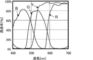
- a color filter is disposed in each pixel of the transmissive liquid crystal display device, and any transmissive liquid crystal display device having a spectral transmittance shown in FIG. 44 is used.
- These transmissive liquid crystal display devices perform display using a backlight (the light source is a cold cathode fluorescent tube [CCFT, CCFL]).
- Table 1 the brightness of the yellow display varies, but this is the brightness of the yellow display when yellow display is performed without turning on the red pixel and the green pixel. Becomes the lowest value (48.0).
- the brightness of the yellow display is the highest value (92.4).
- the brightness of yellow display is an intermediate value.
- FIG. 45 shows the spectral characteristics of a light source used for display of a conventional transmissive liquid crystal display device of four primary colors
- FIG. 46 shows the spectral characteristics of a light source used for display of a conventional transmissive liquid crystal display device of three primary colors.
- the pixels In the conventional transmissive liquid crystal display device of the four primary colors, the pixels have yellow pixels in addition to the red, green and blue pixels. Therefore, when a light source having normal spectral characteristics as shown in FIG. 46 is used, The white display turns yellow. Therefore, in order to adjust the color tone of white display, as shown in FIG.
- a light source with a relatively high bluish color temperature is used.
- high color temperature is realized by increasing blue light emission and reducing green and red light emission.
- the color temperature is increased by increasing the blue component and decreasing the yellow component.
- red, green, and blue LEDs are used, the color temperature is increased by decreasing the green and red components and increasing the blue components, as in CCFT.
- the conventional transmissive liquid crystal display device of four primary colors in order to adjust the color tone of white display, it is necessary to increase the color temperature of the light source and reduce the yellow component and the red component of the light source. The intensity of the red component of the light source is low.
- the visibility is impaired by increasing the number of primary colors used for display, in particular, by reducing the brightness of red.
- a light source having a high color temperature is used to adjust the color tone of white display, it has been found that the brightness of red display is further lowered, and accordingly, the visibility is further impaired.
- the above can be summarized as follows. That is, in the conventional multi-primary color display device including yellow (Ye) pixels, the lightness of the primary color of red is lowered, so that the red display is performed when red display is performed. In the conventional multi-primary color display device including the yellow pixel, the area occupied by the red pixel is smaller than that of the conventional display device using RGB pixels. Furthermore, since yellow pixels are added, the red and green components of the backlight are reduced with respect to the blue component for the purpose of adjusting the white balance. Due to these pixel areas and the spectral characteristics of the backlight, the red brightness is reduced.
- the present invention has been made in view of the above-described situation, and an object of the present invention is to provide a display device that can display a wide color reproduction range and can display bright red.
- the present inventors have made various studies on display devices in which an image is configured using red pixels, green pixels, blue pixels, and yellow pixels.
- the brightness of each color (display color) displayed by devising the light source is devised. Focused on adjusting. And, to improve the lightness of the primary color of red by devising the spectral shape (peak wavelength, half-value width) of the light source, not the magnitude of the peak intensity of each color, which is the spectral characteristic of the light source that is generally noted We studied diligently.
- the present inventors have conducted intensive studies and found that bright red can be displayed by specifying the spectral shape of the light source, and as a result, visibility can be improved.
- the present invention characterized by devising the spectral shape (peak wavelength, full width at half maximum) of light emitted from such a light source can be realized.
- research and development on light sources for display devices such as lights has progressed, and this has contributed to the fact that spectral shape adjustment has become much easier than before.
- Such an effect is not only a transmissive liquid crystal display device in which an image is formed using only red pixels, green pixels, blue pixels, and yellow pixels, but also theoretically red pixels, green pixels, blue pixels. It can be obtained in the same manner in a transmissive liquid crystal display device in which an image is formed using magenta pixels and / or cyan pixels in addition to pixels and yellow pixels, and transmissive liquid crystal
- liquid crystal display devices of other display methods such as a reflective type or a reflective / transmissive type having an auxiliary light source such as a front light, a cathode-ray tube (CRT), an organic electroluminescence display device (Organic) Electro-luminescence display (OELD), plasma display panel (Plasma Display Pa EL: PDP) and various display devices such as surface conduction electron-emitting device displays (Surface-conduction, Electron-emitter Display: SED) and other field emission displays (Field Emission Display: FED).
- the invention described in Patent Document 1 focuses on the brightness of each displayed color (display color) and changes the aperture area of each pixel.
- the spectral shape of the light emitted from the light source is further adjusted to exhibit the effect of significantly improving the redness
- the red brightness can be sufficiently improved.
- one aspect of the present invention is a display device in which an image is configured using red pixels, green pixels, blue pixels, and yellow pixels, and the display device includes a light source and is emitted from the light source.
- Light has a red peak wavelength at 615 nm or more and 650 nm or less, and the half-value width of the red peak is 15 nm or more and 70 nm or less when the peak wavelength is 615 nm or more and 635 nm or less.
- the wavelength is more than 635 nm and not more than 640 nm, it is 40 nm or more and 93 nm or less, and when the peak wavelength is more than 640 nm and 650 nm or less, it is 57 nm or more and 93 nm or less. It is also referred to as a “display device”.
- the present invention can obtain the effect of increasing the brightness of red by changing the spectral shape (peak wavelength, half width) of the light source.
- the effect of improving the redness is made more remarkable, or the area of each pixel is not greatly different, and display defects are sufficiently generated. Can be prevented.
- a display defect is caused by a large difference in the area of each pixel, so that the charging rate, the amount of pixel potential drawn by a gate signal, the amount of variation in pixel potential by a source signal, etc. differ greatly between the pixels. Flicker, burn-in, crosstalk, etc.
- the first to third display devices of the present invention will be described in order.
- the common portions use red pixels, green pixels, blue pixels, and yellow pixels.
- the spectral shape of the light source peak wavelength and / or half width of the peak
- the parts are linked to form a single general inventive concept because they surpass the prior art.
- the red peak wavelength is 615 nm or more.
- the red peak wavelength is preferably 635 nm or less from the viewpoint of further improving the red brightness.
- the peak wavelength refers to the wavelength at which the emission intensity is maximum.
- the dominant wavelength (dominant wavelength) described later refers to a wavelength corresponding to a single wavelength that humans feel when viewing with their eyes.
- an image is configured using red pixels, green pixels, blue pixels, and yellow pixels.
- the “pixel” refers to a minimum element of the display surface to which a color or luminance is independently assigned in a display image.
- the “pixel” may be a picture element (sub-pixel) unless otherwise specified.
- the combination of pixels may not be the same for all combinations of pixels. Further, two or more same colors having different color characteristics may be provided.
- the pixels include pixels that display yellow (yellow pixels) in addition to pixels that display red, green, and blue (red pixels, green pixels, and blue pixels).
- the display device of the present invention since the display device of the present invention has more than three primary colors used for display, it is possible to perform display with a wider color reproduction range than a display device having three primary colors.
- the pixel may include, for example, a pixel (magenta pixel) that displays magenta in addition to the red pixel, the green pixel, the blue pixel, and the yellow pixel.
- magenta pixel it is preferable to have only red pixels, green pixels, blue pixels, and yellow pixels from the viewpoint of the transmittance of the white color filter. If the magenta pixel is included, the transmittance of the magenta pixel is low, and thus there is a possibility that the light use efficiency of the color filter cannot be increased.
- magenta display with high color purity is possible by increasing the color purity of the red and blue pixels. It should be noted that “having only red, green, blue, and yellow pixels” is sufficient if it can be said that it has substantially only red, green, blue, and yellow pixels in the technical field of the present invention. .
- the pixel configuration is not particularly limited, and examples thereof include a stripe arrangement, a diagonal arrangement, and a rice field arrangement.
- the light source is usually used for display, and is preferably a backlight and / or a frontlight.
- the display device of the present invention is preferably a liquid crystal display device.
- a transmissive liquid crystal display device that performs display using a backlight
- a reflective liquid crystal display device that performs display using a front light
- a reflection / transmission liquid crystal display device that performs transmissive display using a backlight and performs reflective display using external light and / or a front light is preferable.
- the light source is a backlight.
- a transmissive liquid crystal display device that performs display using a backlight
- a reflective / transmissive liquid crystal display device that performs transmissive display using a backlight and performs reflective display using external light and / or a front light.
- the backlight may be a direct type backlight or an edge light type backlight.
- a light source using a nanophosphor is preferable.
- a light source such as an organic EL can be used as appropriate.
- the spectrum of the backlight is not the light source itself but the spectrum on the backlight unit in which these light sources are incorporated.
- the spectrum on the backlight unit when the input signal is an all white signal is used.
- the light emitted from the light source refers to the light emitted from the light source device in which the light source is incorporated.
- each pixel is preferably provided with a filter that selectively transmits light in a specific wavelength range (hereinafter also referred to as a “color filter”).
- the display device preferably includes a color filter substrate in which at least a red color filter, a green color filter, a blue color filter, and a yellow color filter are arranged for each pixel.
- the color of the pixel is defined based on the spectral characteristics of the color filter.
- the material of the color filter is not particularly limited, and examples thereof include a resin dyed with a dye, a resin in which a pigment is dispersed, and a fluidized material (ink) in which a pigment is dispersed.
- the color filter can be formed by, for example, a dyeing method, a pigment dispersion method, an electrodeposition method, a printing method, an ink jet method, a colored photosensitive material method (“transfer method”, “dry film lamination (DFL) method” or “dry method”). Also referred to as “film resist method”.
- the following colors are referred to, preferably colors having a dominant wavelength of 600 nm to 640 nm.
- “green” refers to a color having a dominant wavelength of 490 nm to 555 nm, and preferably a color having a dominant wavelength of 510 nm to 550 nm.
- Blue refers to a color having a dominant wavelength of 450 nm to 490 nm, and preferably a color having a dominant wavelength of 450 nm to 475 nm.
- yellow refers to a color having a dominant wavelength of 565 nm to 580 nm, preferably a color having a dominant wavelength of 570 nm to 580 nm. Note that the dominant wavelength and the complementary dominant wavelength roughly represent the hue.
- the red pixel preferably has the largest area among the pixels.
- the brightness of red can be remarkably improved by further maximizing the area of the red pixel.
- the red pixel has the largest area among the pixels, and the green, blue, and yellow pixels have the smallest area. That is, it is preferable that the green, blue, and yellow pixels have the same and minimum area.
- the area of the red and blue pixels is maximum. This also makes it possible to remarkably improve the lightness of red.
- the red and blue pixels are the most numbered among the pixels, and the red and blue pixels have an area per pixel. The form which is the largest and the form which combined these are mentioned.
- the red pixel and the blue pixel are preferable in that conventional pixel design and circuit design can be used because the area of each pixel does not have to be changed according to the form having the largest number of pixels.
- the number of red pixels and blue pixels is the largest among the pixels means that the number of red pixels and blue pixels constituting the pixel is the same and the same as each other. This means that the number of pixels other than the pixels is smaller than the number of red pixels (in other words, the number of blue pixels).
- “different color characteristics” means that at least one of the three attributes of color, hue, brightness, and saturation, is different, and from the viewpoint of efficiently expanding the color reproduction range, Preferably, it means that the hues are different.
- the area of the red pixel and the blue pixel is the maximum and the area of the green pixel and the yellow pixel is the minimum, the transmittance of the white color filter is reduced, but the blue component of the color filter is transmitted. The rate increases relatively. Therefore, in order to optimize the chromaticity of white display, it is possible to reduce the blue component of the light source with low light emission efficiency, and the light emission efficiency of the light source increases, so the white display of the display device including the light emission efficiency of the light source Can be effectively improved. Further, the area of the red pixel and the blue pixel may be the maximum, the area of the green pixel may be the minimum, the area of the red pixel and the blue pixel may be the maximum, and the area of the yellow pixel may be the minimum. May be.
- the areas of the red pixel, the green pixel, the blue pixel, and the yellow pixel are equal. Thereby, it is possible to sufficiently prevent occurrence of defects such as flicker, image sticking, and crosstalk.
- the area of the red pixel is 1 or more times the area of the other color pixel having the smallest area It is preferable that it is 2 times or less. Particularly preferably, it is 1.6 times or less. In other words, the pixel area ratio between the colors of the display device is preferably 1 or more and 1.6 or less.
- the pixel area refers to an area of an area (active area or effective area) used for display, and can also be referred to as an “opening area” in a display device using a color filter.
- the opening area means the area of a region actually used for display, and the area of a light-shielding region by a thin film transistor (TFT), a scanning line, a signal line, an auxiliary capacitor, a black matrix, or the like.
- TFT thin film transistor
- a method of relatively increasing the aperture area of a pixel (1) a method of increasing the aperture area of one pixel, (2) a method of increasing the number of pixels, (3) the method of (1) and the above A combination with the method (2) may be mentioned.
- the method (1) is preferable. This is because according to this method, an increase in the number of switching elements such as thin film transistors (TFTs) for driving each pixel can be suppressed.
- the display device preferably has a color temperature of white light emitted from the display surface of less than 12000K. More preferably, it is 10,000K or less, More preferably, it is 9000K or less.
- the present invention is also a display device in which an image is configured using red pixels, green pixels, blue pixels, and yellow pixels.
- the display device includes a light source, and light emitted from the light source is It is also a display device having a green peak wavelength between 510 nm and 538 nm (hereinafter also referred to as “second display device”).
- the green peak wavelength is preferably 535 nm or less. Also by this, the redness can be improved, and as a result, the visibility of the display device can be improved.
- the green peak wavelength is preferably 520 nm or more. Thereby, the blue saturation fall and the yellow saturation fall can be sufficiently prevented.
- the second display device of the present invention preferably applies the above-described form of the first display device of the present invention (for example, a preferable range of the red peak wavelength and a preferable range of the full width at half maximum). The effect of improving the red brightness can be further improved.
- the present invention is also a display device in which an image is configured using red pixels, green pixels, blue pixels, and yellow pixels.
- the display device includes a light source, and light emitted from the light source is It is also a display device (hereinafter also referred to as “third display device”) having a green peak wavelength at 510 nm or more and 540 nm or less, and a half-value width of the green peak being 57 nm or less. Also by this, the redness can be improved, and as a result, the visibility of the display device can be improved.
- the half width of the green peak is particularly preferably 48 nm or less, for example. For example, it is preferably 30 nm or more.
- the third display device of the present invention can exert the effect of the present invention
- the above-described first display device and second display device of the present invention can be suitably applied.
- Each color pixel may include two or more types of pixels having different color characteristics.
- an image is configured using red pixels, green pixels, blue pixels, and yellow pixels, so that a display with a wide color reproduction range can be performed and emitted from a light source.
- the brightness of red display can be improved by devising the spectral shape of the light.
- FIG. 2 is a plan view schematically showing a TFT substrate in the liquid crystal display device of Embodiment 1.
- FIG. 3 is a plan view schematically showing a counter substrate in the liquid crystal display device of Embodiment 1.
- FIG. 1 is a cross-sectional view schematically showing a liquid crystal display device of Embodiment 1.
- FIG. 6 is a graph showing the relationship between the half-value width (nm) of green and redness (%) in the first embodiment. 6 is a graph showing the relationship between the half-value width (nm) of green and the saturation of blue in the first embodiment. 4 is a graph showing the relationship between the half width of green (nm) and the saturation of yellow in Embodiment 1.
- 10 is a graph showing the relationship between the half value width (nm) of green in Embodiment 2, and red brightness (%).
- 10 is a graph showing the relationship between the half-value width (nm) of green and the saturation of blue in Embodiment 2. It is a graph which shows the relationship between the half value width (nm) of green in Embodiment 2, and the saturation of yellow. It is a graph which shows the relationship between the half value width (nm) of green and red brightness (%) in Embodiment 3.
- 10 is a graph showing the relationship between the half width of green (nm) and the saturation of blue in Embodiment 3.
- 10 is a graph showing the relationship between the half width of green (nm) and the saturation of yellow in Embodiment 3.
- 10 is a graph showing the relationship between the half-value width (nm) of red and redness (%) in Embodiment 4.
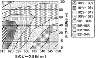
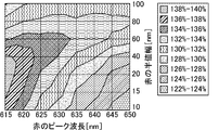
- it is a distribution map which shows red brightness (%) when a vertical axis
- shaft is set to the red half value width (nm) and a horizontal axis is set to the red peak wavelength (nm).
- 10 is a graph showing the relationship between the half width of red (nm) and the saturation of blue in Embodiment 4.
- 14 is a graph showing the relationship between the half width of red (nm) and the saturation of yellow in Embodiment 4.
- 10 is a graph showing the relationship between the half-value width (nm) of red and redness (%) in Embodiment 5.
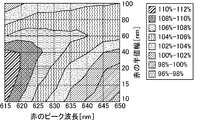
- Embodiment 5 it is a distribution map which shows red lightness (%) when a vertical axis
- 14 is a graph showing the relationship between the half-value width (nm) of red and the redness (%) in Embodiment 6.
- it is a distribution diagram which shows red brightness (%) when a vertical axis
- 18 is a graph showing the relationship between the half width of red (nm) and the red brightness (%) in the seventh embodiment.
- Embodiment 7 it is a distribution map which shows red brightness (%) when a vertical axis
- 10 is a graph showing the relationship between the half-value width (nm) of red and redness (%) in Embodiment 8.
- it is a distribution map which shows red brightness (%) when a vertical axis
- 10 is a graph showing the relationship between the half-value width (nm) of red and the redness (%) in Embodiment 9.
- Embodiment 9 it is a distribution map which shows red lightness (%) when a vertical axis
- Embodiment 10 it is a distribution map which shows red lightness (%) when a vertical axis
- Embodiment 11 it is a distribution map which shows red brightness (%) when the vertical axis
- Embodiment 12 it is a distribution map which shows red brightness (%) when a vertical axis
- FIG. 34 is a plan view schematically showing a counter substrate in the liquid crystal display device of Embodiment 13.
- FIG. 34 is a plan view schematically showing a counter substrate in the liquid crystal display device of Embodiment 13.
- FIG. 20 is a cross-sectional view schematically showing a liquid crystal display device of Embodiment 13. It is a graph which shows the relationship between the half value width (nm) of red in Embodiment 13, and red brightness (%). In Embodiment 13, it is a distribution map which shows red lightness (%) when a vertical axis
- FIG. 25 is a plan view schematically showing a counter substrate in the liquid crystal display device of Embodiment 14.
- FIG. 16 is a cross-sectional view schematically showing a liquid crystal display device of Embodiment 14.
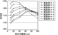
- Embodiment 14 It is a graph which shows the relationship between the half value width (nm) of red in Embodiment 14, and red brightness (%).
- Embodiment 14 it is a distribution map which shows red brightness (%) when a vertical axis
- 4 is a graph showing the relationship between the wavelength (nm) and the intensity representing the backlight spectrum used in Example 1-3. It is a graph which shows the relationship between the wavelength (nm) showing the spectrum of the backlight used in Example 5-4, and intensity
- the “half-value width” refers to the width between wavelengths on both sides of the peak wavelength where the intensity becomes half-value compared to the peak wavelength.
- the half-value width is set to twice the difference between the half-value wavelength on one side and the peak wavelength.
- pixel combination refers to a basic unit for display in which a plurality of color pixels are combined, and this may be simply referred to as “pixel” in the technical field of the present invention. .
- the redness (%) is the conventional redness (comparative example of Reference Example 2-1 described later) (green peak wavelength of backlight light source spectrum is 540 nm, half-value width is 58 nm, This is a value in which the peak wavelength of red is 640 nm and the half width is 97 nm.
- FIG. 1 is a plan view schematically showing a TFT substrate in the liquid crystal display device of Embodiment 1.
- the TFT substrate 30 has a matrix wiring composed of scanning lines 4 and signal lines 6 arranged on a glass substrate, and a thin film transistor (TFT) 8 is provided at each intersection of the matrix wirings.
- the transparent electrodes 35 35R, 35G, 35B, and 35Y
- a transparent conductive material such as indium tin oxide (ITO)
- the gate electrode of the TFT 8 is connected to the scanning line 4, the source electrode is connected to the signal line 6, and the drain electrode is connected to the transparent electrode 35 via the drain lead wiring 9.
- the transparent electrodes 35R, 35G, 35B, and 35Y are respectively opposed to red, green, blue, and yellow color filters 10R, 10G, 10B, and 10Y provided on a counter substrate 20 described later in the liquid crystal display device. It is provided as follows. In the present embodiment, as shown in FIG. 1, the scanning lines 4 and the signal lines 6 are arranged so that the transparent electrodes 35R, 35G, 35B, and 35Y have the same size.
- the auxiliary capacitance wiring 7 for holding the voltage applied to the transparent electrode 35 is arranged in parallel with the scanning line 4.
- the auxiliary capacitance line 7 constitutes the auxiliary capacitance 3 by facing the end portion of the drain lead line 9 through the insulating film.
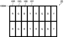
- FIG. 2 is a plan view schematically showing a color filter substrate (counter substrate) in the liquid crystal display device of the first embodiment.
- the counter substrate 20 has red, green, blue, and yellow color filters 10R, 10G, 10B, and 10Y arranged in stripes in this order, and a black matrix 10BM is formed between the filters.
- Each of the color filters 10R, 10G, 10B, and 10Y selects the color of light that passes through itself.
- the red, green, and blue color filters 10R, 10G, and 10B mainly transmit the red component, the green component, and the blue component of incident light, respectively.
- the yellow color filter 10Y mainly transmits both the red color component and the green color component of incident light.
- the color filters 10R, 10G, 10B, and 10Y are provided to face the transparent electrodes 35R, 35G, 35B, and 35Y provided on the TFT substrate 30 in the liquid crystal display device, respectively.
- the black matrix 10BM is provided to face the scanning lines 4 and the signal lines 6 in the liquid crystal display device.
- FIG. 3 is a cross-sectional view schematically showing the liquid crystal display device of the first embodiment.
- the liquid crystal display device 50 according to the first embodiment of the present invention has a configuration in which a liquid crystal layer 40 is sandwiched between the counter substrate 20 and the TFT substrate 30 described above.
- the counter substrate 20 includes a phase difference plate 22 and a polarizing plate 23 on the outer side (observation surface side) of the glass substrate 21, and red, green, blue, and yellow on the inner side (back side) of the glass substrate 21.
- the phase difference plate 22 adjusts the polarization state of light that passes through the retardation plate 22.
- the polarizing plate 23 transmits only light of a specific polarization component.
- the viewing angle compensation function is provided by adjusting the arrangement and configuration of the retardation film 22 and the polarizing plate 23.
- the overcoat layer 25 prevents contaminants from eluting into the liquid crystal layer 40 from the red, green, blue, and yellow color filters 10R, 10G, 10B, and 10Y. Flattening.
- the counter electrode 26 is opposed to the transparent electrodes 35R, 35G, 35B, and 35Y provided on the TFT substrate 30 side through the liquid crystal layer 40, and a voltage is applied to the liquid crystal layer 40 to cause liquid crystal molecules to flow. Used to drive.
- the counter electrode 26 is made of a transparent conductive material such as indium tin oxide (ITO).
- the alignment film 27 controls the alignment of the liquid crystal molecules in the liquid crystal layer 40.
- the TFT substrate 30 includes a phase difference plate 32 and a polarizing plate 33 on the outer side (back side) of the glass substrate 31, and a thin film transistor (TFT) 8 and an interlayer on the inner side (observation side) of the glass substrate 31.
- An insulating film 34, a transparent electrode 35 (35R, 35G, 35B, and 35Y), an alignment film 38, and the like are provided.
- the phase difference plate 32 adjusts the polarization state of the light that passes through the retardation plate 32, as in the phase difference plate 22.
- the polarization plate 33 transmits only light of a specific polarization component, like the polarization plate 23. It is something to be made.
- the polarizing plate 33 is disposed so as to be optically orthogonal to the polarizing plate disposed on the counter substrate 20 side.
- the transparent electrode 35 (35R, 35G, 35B, and 35Y) is arranged for each color filter on the counter substrate 20, and drives the liquid crystal molecules by applying a voltage to the liquid crystal layer 40 for each color filter region. To do.
- the alignment film 38 controls the alignment of the liquid crystal molecules in the liquid crystal layer 40 in the same manner as the heel alignment film 27.
- a backlight 36 used for display is provided on the back side (back side) of the TFT substrate 30.
- a backlight 36 used for display is provided on the back side (back side) of the TFT substrate 30.
- the spectral characteristics of the light source used for the backlight 36 will be described in detail later.
- nematic liquid crystal is used as the material of the liquid crystal layer 40.
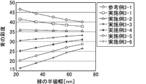
- Table 3 shows the green peak wavelength (nm) and full width at half maximum (23 nm, 35 nm, 48 nm, 58 nm, and 70 nm, respectively) in Embodiment 1 (Examples 1-1 to 1-6, Reference Example 1-1). ), A red peak wavelength (nm), and a full width at half maximum (nm).
- Reference Example 1-1 is a comparative example when the half-value width of green is 58 nm and 70 nm.
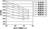
- FIG. 4 is a graph showing the relationship between the half-value width (nm) of green and redness (%) in the first embodiment.
- the red peak wavelength ⁇ p of the spectrum of the backlight light source is 645 nm
- the half-value width is 97 nm.
- the peak wavelength ⁇ p of red is 645 nm
- the brightness of red is increased by shortening the peak wavelength of green (G), for example, by setting it to 538 nm or less.
- the green light emitted from the backlight that has been used for conventional four-primary-color display has a peak wavelength of 540 nm and a half-value width of approximately 60 nm (58 nm or more).
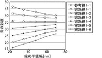
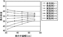
- FIG. 5 is a graph showing the relationship between the half width (nm) of green and the saturation of blue in the first embodiment.
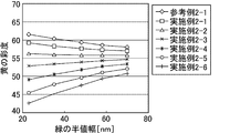
- FIG. 6 is a graph showing the relationship between the half width (nm) of green and the saturation of yellow in the first embodiment.
- the lower the green peak wavelength ⁇ p the higher the red brightness, for example, when ⁇ p ⁇ 515 nm.
- the saturation of blue display occurs, and the saturation of yellow display occurs as shown in FIG. 6. Therefore, it is preferable that ⁇ p ⁇ 520 nm. More preferably, ⁇ p ⁇ 525 nm.
- Embodiment 2 Table 4 below shows the green peak wavelength (nm) and half-value width (23 nm, 35 nm, 48 nm, 58 nm, and 70 nm, respectively) in Embodiment 2 (Example 2-1 to Example 2-6, Reference Example 2-1). ), A red peak wavelength (nm), and a full width at half maximum (nm).
- Reference Example 2-1 is a comparative example when the half-value width of green is 58 nm and 70 nm.
- FIG. 7 is a graph showing the relationship between the half-value width (nm) of green and redness (%) in the second embodiment.
- the configuration of the second embodiment is the same as the configuration of the first embodiment except that the red peak wavelength ⁇ p of the spectrum of the backlight light source is 640 nm instead of 645 nm.
- the peak wavelength ⁇ p of red (R) is 640 nm
- the brightness of red is increased by shortening the peak wavelength of green (G), for example, 538 nm or less.
- the peak wavelength of green (G) is 535 nm or less. In the comparison of the same green peak wavelength, as shown in FIG.
- FIG. 8 is a graph showing the relationship between the half width (nm) of green and the saturation of blue in the second embodiment.
- FIG. 9 is a graph showing the relationship between the half width (nm) of green and the saturation of yellow in the second embodiment.
- ⁇ p of green (G) decreases, for example, when ⁇ p ⁇ 515 nm, the red brightness is further increased.
- the saturation of the blue display occurs, and the saturation of the yellow display occurs as shown in FIG. 9. Therefore, it is preferable that ⁇ p ⁇ 520 nm. More preferably, ⁇ p ⁇ 525 nm.
- Embodiment 3 Table 5 below shows the green peak wavelength (nm) and half-value width (23 nm, 35 nm, 48 nm, 58 nm, and 70 nm, respectively) in Embodiment 3 (Examples 3-1 to 3-6, Reference Example 3-1). ), A red peak wavelength (nm), and a full width at half maximum (nm).
- Reference Example 3-1 is a comparative example when the half-value width of green is 58 nm and 70 nm.
- FIG. 10 is a graph showing the relationship between the half-value width (nm) of green and redness (%) in the third embodiment.
- the configuration of the third embodiment is the same as the configuration of the first embodiment except that the red peak wavelength ⁇ p of the spectrum of the backlight light source is 635 nm instead of 645 nm.
- the peak wavelength ⁇ p of red (R) is 635 nm
- the brightness of red is increased by shortening the peak wavelength of green (G), for example, by setting it to 538 nm or less.
- the peak wavelength of green (G) is 535 nm or less.
- the effect of improving the brightness of red increases as the half-value width decreases.
- FIG. 11 is a graph showing the relationship between the half-value width (nm) of green and the saturation of blue in the third embodiment.
- FIG. 12 is a graph illustrating the relationship between the half width of green (nm) and the saturation of yellow in the third embodiment.
- ⁇ p of green (G) decreases, for example, when ⁇ p ⁇ 515 nm, the red brightness is further increased.
- the saturation of blue display occurs, and the saturation of yellow display occurs as shown in FIG. 12. Therefore, it is preferable that ⁇ p ⁇ 520 nm. More preferably, ⁇ p ⁇ 525 nm.
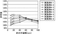
- Table 6 shows the green peak wavelength (nm), half-value width (nm), red peak wavelength (nm), and half-value width (each 10 nm in the fourth embodiment (Examples 4-1 to 4-8). , 15 nm, 20 nm, 40 nm, 60 nm, 80 nm, 100 nm).
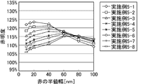
- FIG. 13 is a graph showing the relationship between the red half-value width (nm) and red brightness (%) in the fourth embodiment.
- the peak wavelength of 535 nm and the half-value width of 58 nm of green (G) that does not deteriorate the display quality of yellow (Y) and blue (B) the peak wavelength and half-value width of red (R) that further increases the brightness of red was examined. There is a full width at half maximum for increasing the red brightness for each peak wavelength of red.
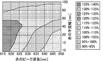
- FIG. 14 is a distribution diagram showing red brightness (%) when the vertical axis is the red half-value width (nm) and the horizontal axis is the red peak wavelength (nm) in the fourth embodiment.
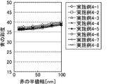
- FIG. 15 is a graph showing the relationship between the half width (nm) of red and the saturation of blue in the fourth embodiment.
- FIG. 16 is a graph showing the relationship between the half width (nm) of red and the saturation of yellow in the fourth embodiment.
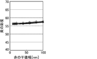
- the influence of red peak wavelength, half-value width on blue saturation and yellow saturation is small.
- Embodiments 5 to 9 which will be described later, a graph showing the relationship between the half width of red (nm) and the saturation of blue and a graph showing the relationship between the half width of red (nm) and the saturation of blue are shown. There is no effect on blue saturation and yellow saturation as well. Note that the configuration not particularly specified in the fourth embodiment is the same as the configuration shown in the first embodiment.
- Table 7 shows the green peak wavelength (nm), the half-value width (nm), the red peak wavelength (nm), and the half-value width (each 10 nm in the embodiment 5 (Examples 5-1 to 5-8). , 15 nm, 20 nm, 40 nm, 60 nm, 80 nm, 100 nm).
- FIG. 17 is a graph showing the relationship between the red half-value width (nm) and red brightness (%) in the fifth embodiment.
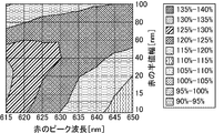
- FIG. 18 is a distribution diagram showing red brightness (%) when the vertical axis is the red half-value width (nm) and the horizontal axis is the red peak wavelength (nm) in the fifth embodiment.
- the configuration of the fifth embodiment is the same as the configuration of the fourth embodiment except that the green peak wavelength ⁇ p of the spectrum of the backlight light source is 530 nm instead of 535 nm.
- Table 8 shows the green peak wavelength (nm), half-value width (nm), red peak wavelength (nm), and half-value width (each 10 nm in Example 6 (Examples 6-1 to 6-8)). , 15 nm, 20 nm, 40 nm, 60 nm, 80 nm, 100 nm).
- FIG. 19 is a graph showing the relationship between the red half-value width (nm) and red brightness (%) in the sixth embodiment.
- FIG. 20 is a distribution diagram showing red lightness (%) when the vertical axis is red half-value width (nm) and the horizontal axis is red peak wavelength (nm) in the sixth embodiment.
- the configuration of the sixth embodiment is the same as that of the fourth embodiment except that the green peak wavelength ⁇ p of the spectrum of the backlight light source is 525 nm instead of 535 nm.
- Table 9 shows the green peak wavelength (nm), half-value width (nm), red peak wavelength (nm), and half-value width (each 10 nm in Embodiment 7 (Examples 7-1 to 7-8)). , 15 nm, 20 nm, 40 nm, 60 nm, 80 nm, 100 nm).
- FIG. 21 is a graph showing the relationship between the red half-value width (nm) and red brightness (%) in the seventh embodiment.
- FIG. 22 is a distribution diagram showing red brightness (%) when the vertical axis is the red half-value width (nm) and the horizontal axis is the red peak wavelength (nm) in the seventh embodiment.
- the configuration of the seventh embodiment is the same as the configuration of the fourth embodiment except that the half width of the green spectrum of the backlight source is set to 48 nm instead of 58 nm.
- Table 10 shows the green peak wavelength (nm), half-value width (nm), red peak wavelength (nm), and half-value width (each 10 nm in the eighth embodiment (Example 8-1 to Example 8-8). , 15 nm, 20 nm, 40 nm, 60 nm, 80 nm, 100 nm).
- FIG. 23 is a graph showing the relationship between the red half-value width (nm) and red brightness (%) in the eighth embodiment.
- FIG. 24 is a distribution diagram showing the red brightness (%) when the vertical axis is the red half width (nm) and the horizontal axis is the red peak wavelength (nm) in the eighth embodiment.
- the configuration of the eighth embodiment is the same as the configuration of the fourth embodiment except that the half width of the green spectrum of the backlight source is set to 35 nm instead of 58 nm.
- green (G) of Examples 1-1 to 1-3 also green (G) of Examples 2-1 to 2-3 or green (G) of Examples 3-1 to 3-3).
- the red (R) peak wavelength and full width at half maximum the red brightness is significantly improved to 110% or more compared to the conventional one. It is particularly preferable to adjust the red (R) spectral shape together with the green (G) spectral shape so that the red brightness is 110% or more.
- the green (G) light emitted from the light source has a green peak wavelength between 510 nm and 535 nm, and the light emitted from the light source is 510 nm, which is a general wavelength range for green light.
- the green peak wavelength is 550 nm or less and the half-value width of the green peak is 57 nm or less.
- the peak wavelength of green (G) light is 525 nm or more. preferable.
- the peak wavelength of green (G) light is preferably set to 540 nm or less.
- the half width of green (G) light is 50 nm or less. More preferably, it is 35 nm or less.
- the red (R) light emitted from the light source preferably has a red peak wavelength of 615 nm or more and 650 nm or less, and the half-value width of the red peak is preferably 10 nm to 100 nm.
- a suitable red spectrum shape (peak wavelength range, half width range) in the first display device of the present invention is added to a suitable form of the spectral shape (peak wavelength range, half width range) of green (G) light.
- the applied form is particularly suitable.
- a display device in which both the red spectrum shape and the green spectrum shape are adjusted is particularly preferable, and the effects of the present invention can be made significantly superior.
- Table 11 shows the green peak wavelength (nm), half-value width (nm), red peak wavelength (nm), and half-value width (each 10 nm in Example 9 (Examples 9-1 to 9-8)). , 15 nm, 20 nm, 40 nm, 60 nm, 80 nm, 100 nm).
- FIG. 25 is a graph showing the relationship between the red half-value width (nm) and red brightness (%) in the ninth embodiment.
- FIG. 26 is a distribution diagram showing red brightness (%) when the vertical axis is the red half-value width (nm) and the horizontal axis is the red peak wavelength (nm) in the ninth embodiment.
- the configuration of the ninth embodiment is the same as the configuration of the fourth embodiment except that the green peak wavelength ⁇ p of the backlight light source spectrum is set to 540 nm instead of 535 nm.
- the red brightness can be compared with the conventional one. 100% or more.
- the brightness of red differs depending on the green (G) spectral shape and the red (R) spectral shape of the backlight. Further, it varies depending on the aperture ratio of each pixel and the set temperature of white balance. By increasing the red aperture ratio and decreasing the white balance color temperature, the brightness of red increases.
- Embodiments 1 to 9 described above the effects in the case where the aperture ratios are equal and the color temperature of the white balance is 10,000 K have been described.
- the effect of increasing the brightness of red according to the first to ninth embodiments can be exhibited even in the case of other aperture ratios and other white balance color temperatures.
- Embodiments showing the effect of red brightness at other aperture ratios and white balance color temperatures will be described in detail in Embodiments 10 to 14 below.
- Table 12 below shows the green peak wavelength (nm), half-value width (nm), red peak wavelength (nm), and half-value width (each 10 nm in Example 10 (Examples 10-1 to 10-8)). , 15 nm, 20 nm, 40 nm, 60 nm, 80 nm, 100 nm).
- FIG. 27 is a graph showing the relationship between the red half-value width (nm) and red brightness (%) in the tenth embodiment.
- FIG. 28 is a distribution diagram showing the red brightness (%) when the vertical axis is the red half width (nm) and the horizontal axis is the red peak wavelength (nm) in the tenth embodiment.
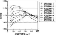
- Table 13 below shows the green peak wavelength (nm), half-value width (nm), red peak wavelength (nm), and half-value width (each 10 nm in Embodiment 11 (Examples 11-1 to 11-8)). , 15 nm, 20 nm, 40 nm, 60 nm, 80 nm, 100 nm).
- FIG. 29 is a graph showing the relationship between the red half-value width (nm) and red brightness (%) in the eleventh embodiment.
- FIG. 30 is a distribution diagram showing the red brightness (%) when the vertical axis is the red half-value width (nm) and the horizontal axis is the red peak wavelength (nm) in the eleventh embodiment.
- Embodiment 12 Table 14 below shows the green peak wavelength (nm), half-value width (nm), red peak wavelength (nm), and half-value width (each 10 nm in Example 12 (Examples 12-1 to 12-8)). , 15 nm, 20 nm, 40 nm, 60 nm, 80 nm, 100 nm).
- FIG. 31 is a graph showing the relationship between the red half-value width (nm) and red brightness (%) in the twelfth embodiment.
- FIG. 32 is a distribution diagram showing the redness (%) when the vertical axis is the red half width (nm) and the horizontal axis is the red peak wavelength (nm) in the twelfth embodiment.
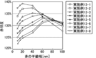
- Table 15 below shows the green peak wavelength (nm), half-value width (nm), red peak wavelength (nm), and half-value width (each 10 nm in the embodiment 13 (Examples 13-1 to 13-8). , 15 nm, 20 nm, 40 nm, 60 nm, 80 nm, 100 nm).
- FIG. 33 is a plan view schematically showing a counter substrate in the liquid crystal display device of Embodiment 13.
- FIG. 34 is a cross-sectional view schematically showing a liquid crystal display device according to the thirteenth embodiment.
- the configuration is the same as that of the ninth embodiment.
- members and portions that exhibit the same functions as those shown in FIG. 2 and FIG. 3 are given the same reference numerals except that 1 is added to the hundreds.
- FIG. 35 is a graph showing the relationship between the red half-value width (nm) and red brightness (%) in the thirteenth embodiment.
- FIG. 36 is a distribution diagram showing the redness (%) when the vertical axis represents the red half width (nm) and the horizontal axis represents the red peak wavelength (nm) in the thirteenth embodiment.
- the peak wavelength and the half-value width of red (R) for increasing the brightness of red are examined for the conventional Green peak wavelength of 540 nm and the half-value width of 58 nm.
- Table 16 shows the green peak wavelength (nm), half-value width (nm), red peak wavelength (nm), and half-value width (each 10 nm in Example 14 (Examples 14-1 to 14-8)). , 15 nm, 20 nm, 40 nm, 60 nm, 80 nm, 100 nm).
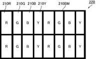
- FIG. 37 is a plan view schematically showing a counter substrate in the liquid crystal display device according to the fourteenth embodiment.
- FIG. 38 is a cross-sectional view schematically showing the liquid crystal display device of Embodiment 14.
- the configuration is the same as that of the ninth embodiment.
- members and parts that exhibit the same functions as those shown in FIGS. 2 and 3 are given the same reference numerals except that twos are added to the hundreds.
- FIG. 39 is a graph showing the relationship between the red half-value width (nm) and the red brightness (%) in the fourteenth embodiment.
- FIG. 40 is a distribution diagram showing redness (%) when the vertical axis is the red half width (nm) and the horizontal axis is the red peak wavelength (nm) in the fourteenth embodiment.
- the peak wavelength and the half-value width of red (R) for increasing the lightness of red are examined for a green peak wavelength of 540 nm and a half-value width of 58 nm.
- the effect of the present invention such as that the red brightness becomes 100% or more by comparing the red (R) peak wavelength and the full width at half maximum with the conventional configuration. It can be demonstrated.
- a display device in which an image is configured using red pixels, green pixels, blue pixels, and yellow pixels the display device including a light source, and light emitted from the light source.
- the full width at half maximum of the red peak is 15 nm or more when the peak wavelength is 615 nm or more and 625 nm or less, and is 30 nm or more when the peak wavelength is more than 625 nm and 635 nm or less.
- a display device Thereby, the redness can be further improved.
- the red brightness is improved as the color temperature of white emitted from the display surface is decreased.
- the red brightness can be improved as the aperture ratio of each pixel is increased from red / blue to green / yellow.
- the red brightness in the conventional spectrum (green [G] peak wavelength 540 nm, half-value width 58 nm, red [R] peak wavelength 640 nm, half-value width 100 nm) is 100.0%, respectively.
- Example 9-6) ⁇ 103.7% (Example 10-6) ⁇ 109.1% (Example 11-6) ⁇ 120.4% (Example 12-6) ⁇ 131.4% (implementation)
- Example 13-6) ⁇ 117.1% (Example 14-6). For embodiments that exceed this value, there is an effect of the present invention.
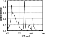
- FIG. 41 is a graph showing the relationship between wavelength (nm) and intensity representing the spectrum of the backlight used in Example 1-3.
- the spectral shapes of green (G) and red (R) are as follows. Green (G): Peak wavelength 530 nm, half width 58 nm Red (R): Peak wavelength 640 nm, half-value width 100 nm
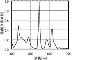
- FIG. 42 is a graph showing the relationship between the wavelength (nm) and the intensity representing the spectrum of the backlight used in Example 5-4.
- the spectral shapes of green (G) and red (R) are as follows. Green (G): Peak wavelength 530 nm, half width 58 nm Red (R): Peak wavelength 640 nm, half width 58 nm
- FIG. 43 is a graph showing the relationship between the wavelength (nm) and the intensity representing the spectrum of the backlight used in Reference Example 1-1.
- the spectral shapes of green (G) and red (R) are as follows. Green (G): Peak wavelength 540 nm, half width 58 nm Red (R): Peak wavelength 640 nm, half-value width 100 nm
- the three wavelengths of the wavelength having the maximum intensity, the wavelength having the second intensity, and the wavelength having the third intensity in the radiant intensity of the backlight spectrum are roughly 400 nm to 500 nm, 500 nm to 500 nm, for example. It is divided into three regions corresponding to blue, green and red, such as 600 nm and 600 nm to 700 nm.
- the peak wavelength of blue is 440 nm to 460 nm, and the full width at half maximum of blue is better and is preferably 30 nm or less.
- the saturation of blue and yellow (C * ) is represented by ⁇ (a * ) 2 + (b * ) 2 ⁇ 0.5 as defined in CIE1976. Note that a * and b * indicate the color direction in the chromaticity diagram, a * indicates the red direction, and b * indicates the yellow direction. If the saturation of blue is 25 or more and the saturation of yellow is 40 or more, the display product is good.
- the spectral transmittance characteristics of each color display of the liquid crystal layer are expressed as follows. That is, the white transmittance spectral transmittance characteristic of the liquid crystal layer is LCDw ( ⁇ ), and the black transmittance spectral transmittance characteristic of the liquid crystal layer is LCDbk ( ⁇ ). Also, the spectral transmittance characteristic of the red color filter is CFr ( ⁇ ), the spectral transmittance characteristic of the green color filter is CFg ( ⁇ ), the spectral transmittance characteristic of the blue color filter is CFb ( ⁇ ), and the yellow color filter Is assumed to be CFy ( ⁇ ), and the spectral transmittance characteristic of the cyan color filter is assumed to be CFc ( ⁇ ).
- a white display spectrum of a display device using an arbitrary backlight spectrum BL1 ( ⁇ ) is obtained by the following equation (1).
- White ( ⁇ ) ⁇ Pr ⁇ CFr ( ⁇ ) ⁇ LCDw ( ⁇ ) + Pg ⁇ CFg ( ⁇ ) ⁇ LCDw ( ⁇ ) + Pb ⁇ CFb ( ⁇ ) ⁇ LCDw ( ⁇ ) + Py ⁇ CFy ( ⁇ ) ⁇ LCDw ( ⁇ ) + Pc ⁇ CFc ( ⁇ ) ⁇ LCDbk ( ⁇ ) ⁇ ⁇ BL1 ( ⁇ ) (Formula 1)
- the white display chromaticity (xw, yw) is based on the CIE color system and the white display tristimulus values Xw, Yw, Zw are obtained from the white display wavelength characteristic White ( ⁇ ) obtained by (Equation 1).
- the chromaticity (xw, yw) for white display is obtained by calculating and using these Xw, Yw, and Zw.
- the chromaticity of the white display becomes a predetermined value by changing the height of the peak of the R region and G region of the backlight. Adjust so that The spectrum of the backlight after this adjustment is BL2 ( ⁇ ).
- the other display colors are calculated by the following (Expression 2) to (Expression 6) using the backlight spectrum BL2 ( ⁇ ) after adjusting the chromaticity of white display.
- Red ( ⁇ ) ⁇ Pr ⁇ CFr ( ⁇ ) ⁇ LCDw ( ⁇ ) + Pg ⁇ CFg ( ⁇ ) ⁇ LCDbk ( ⁇ ) + Pb ⁇ CFb ( ⁇ ) ⁇ LCDbk ( ⁇ ) + Py ⁇ CFy ( ⁇ ) ⁇ LCDbk ( ⁇ ) + Pc ⁇ CFc ( ⁇ ) ⁇ LCDbk ( ⁇ ) ⁇ ⁇ BL2 ( ⁇ ) (Formula 2)
- the chromaticity coordinate x of the red display color may be less than 0.64 depending on BL2 ( ⁇ ).
- CFr ( ⁇ ) was readjusted so that the chromaticity coordinate x of the red display color was 0.64 or more.
- the peak wavelength of LED light emission type green (G) is 530 nm and the half value width of 32 nm.
- the peak wavelength of red (R) is 630 nm and the half width is 17 nm.
- the peak wavelength of green (G) of the fluorescent emission type currently used is 539 nm and the half width of 59 nm.
- the peak wavelength of red (R) is 638 nm and the half width is 97 nm.
- both LED light-emitting backlights and fluorescent light-emitting backlights may cause variations of about ⁇ 3 nm in peak wavelength and half-value width due to individual differences.
- a cold cathode fluorescent tube CCFT, CCFL
- a white light emitting diode (combination of blue light emitting LED and yellow fluorescent light emission)
- RGB-LED hot cathode fluorescent tube
- organic EL field emission display (FED), or the like
- FED field emission display
- a transmissive liquid crystal display device that performs display using a backlight
- the present invention is not limited to a transmissive liquid crystal display device, and is transmissive using a backlight.
- Other display methods such as a reflection / transmission liquid crystal display device that performs display and performs reflection display using external light and / or a front light, and a reflective liquid crystal display device that performs display using a light source such as a front light Liquid crystal display devices, cathode ray tube (CRT), organic electroluminescence display device (OELD), plasma display panel (PDP), and field emission display (FED) such as surface conduction electron-emitting device display (SED) It is used suitably for this display device.
- “above” and “below” include the numerical values (boundary values).
- Auxiliary capacitor 4 Scan line 6: Signal line 7: Auxiliary capacitor (Cs) wiring 8: Thin film transistor (TFT) 9: Drain lead wires 10R, 110R, 210R: Red color filters 10G, 110G, 210G: Green color filters 10B, 110B, 210B: Blue color filters 10Y, 110Y, 210Y: Yellow color filters 10BM, 110BM, 210BM : Black matrix (blacked area) 20, 120, 220: Color filter substrate (counter substrate) 21, 31, 121, 131, 221, 231: Glass substrate 22, 32, 122, 132, 222, 232: Retardation plates 23, 33, 123, 133, 223, 233: Polarizing plates 25, 125, 225: Over Coat layers 26, 126, 226: counter electrodes 27, 38, 127, 138, 227, 238: alignment films 30, 130, 230: thin film transistor (TFT) substrates 34, 134, 234: interlayer insulating films 35, 135, 235: Trans
Landscapes
- Physics & Mathematics (AREA)
- Nonlinear Science (AREA)
- Mathematical Physics (AREA)
- Chemical & Material Sciences (AREA)
- Crystallography & Structural Chemistry (AREA)
- General Physics & Mathematics (AREA)
- Optics & Photonics (AREA)
- Liquid Crystal (AREA)
- Optical Filters (AREA)
Abstract
本発明は、色再現範囲の広い表示が可能であるとともに、明るい赤を表示することができる表示装置を提供する。本発明の表示装置は、赤画素、緑画素、青画素、及び、黄画素を用いて画像が構成され、光源を備え、上記光源から射出される光は、615nm以上、650nm以下に赤色のピーク波長があり、上記赤色のピークの半値幅は、該ピーク波長が615nm以上、635nm以下である場合は、15nm以上、70nm以下であり、該ピーク波長が635nmを超え、640nm以下である場合は、40nm以上、93nm以下であり、該ピーク波長が640nmを超え、650nm以下である場合は、57nm以上、93nm以下である。
Description
本発明は、表示装置に関する。より詳しくは、赤画素、緑画素、青画素、及び、黄画素を用いて画像が構成される液晶表示装置に好適に用いられる表示装置に関するものである。
表示装置としては、画素により画像を形成する各種のディスプレイが情報や映像の表示手段として広く普及している。中でも、1つの画素が複数原色のサブピクセルによって構成され、これによりカラー表示する液晶表示パネル、有機EL(Electroluminescence)表示パネル等の表示パネルが一般的である。
一般的な表示装置では、光の三原色である赤、緑及び青を表示する3色の画素によって画像が構成されており、カラー表示が可能になっている。これに対し、表示可能な色の範囲(色再現範囲)を拡大することを目的として、赤、緑及び青のサブ画素にカラーフィルタの透過率の高い黄のサブ画素を加えた多原色の表示装置が提案されている。この表示装置によれば、カラーフィルタの透過率の高い黄のサブ画素が加えられていることから、白表示の明度の低下を抑制することができるとともに、表示に用いる原色の数が増えることから、色再現範囲を拡大することができる。
例えば、赤、緑、青及び黄のサブ画素を有する画素によって表示面が構成された表示装置であって、該赤のサブ画素は、開口面積が最大であることを特徴とする表示装置が開示されている(例えば、特許文献1参照。)。
ところで、近年においては、液晶表示装置用バックライト等に好適に適用できるナノ蛍光体や、半導体発光素子等の、表示装置用の光源が新たに研究開発されている(例えば、特許文献2、3参照。)。
赤画素、緑画素、青画素及び黄画素を用いて画像が構成される表示装置と、赤画素、緑画素及び青画素によって画像が構成される表示装置の明度等に関する光学的特性について、以下に詳細に検討する。例えば、それぞれの開口面積が等しい赤画素、緑画素、青画素及び黄画素を用いて画像が構成される従来の4原色の透過型液晶表示装置においては、各表示色の明度は表1に示すようになる。また、それぞれの開口面積が等しい赤、緑及び青の3つの画素からなる画素によって表示面が構成された従来の3原色の透過型液晶表示装置においては、各表示色の明度は表2に示すようになる。


表1及び表2にはそれぞれ、代表的な表示色として、赤、緑、青、黄、シアン及びマゼンタの6色の明度について示している。また、各表示色の明度は、CIE 1931(標準)表色系(XYZ表色系)におけるY値に相当し、白表示の明度を100としたときの値である。更に、透過型液晶表示装置の各画素には、カラーフィルタが配置されており、いずれの透過型液晶表示装置においても、図44に示す分光透過率を有するものを用いている。そして、これらの透過型液晶表示装置は、バックライト(光源は、冷陰極蛍光管〔CCFT、CCFL〕)を用いて表示を行うものとし、この光源の分光特性は、白表示の色度がx=0.313、y=0.329となり、色温度が6500Kとなるように、適切に調節されている。なお、表1においては、黄表示の明度に幅があるが、これは、黄の画素を点灯させ、赤の画素及び緑の画素を点灯させないで黄表示を行う場合には、黄表示の明度は最も低い値(48.0)になり、黄の画素に加え、赤の画素及び緑の画素を点灯させて黄表示を行う場合には、黄表示の明度は最も高い値(92.4)になり、赤の画素、緑の画素及び黄の画素をそれぞれ適切な割合で点灯させて黄表示を行う場合には、黄表示の明度は中間の値となることを示している。
表1及び表2の結果より、従来の4原色の透過型液晶表示装置が、赤表示、緑表示及び青表示の明度とも従来の3原色の透過型液晶表示装置よりも低くなっていることを見いだした。これは、表示に用いる原色の数を増やすことにより、画素の数が増え、画素1つ当たりの面積が相対的に小さくなっていることに起因する。すなわち、表示に用いる原色の数を3つから4つに増やすことにより、各画素の面積は3/4となっているからである。更に、このような各表示色の明度の低下について検討したところ、緑表示や青表示については、明度が低下しても視認性が損なわれることはないが、赤表示については、明度が低下することにより、どす黒い赤すなわち暗い赤となるため、視認性が損なわれやすい。
次に、本発明者らは、従来の4原色の透過型液晶表示装置の表示に用いられる光源の分光特性に着目した。従来の4原色の透過型液晶表示装置の表示に用いられる光源の分光特性を図45に示し、従来の3原色の透過型液晶表示装置の表示に用いられる光源の分光特性を図46に示す。従来の4原色の透過型液晶表示装置では、画素が赤、緑及び青の画素に加えて、黄の画素を有することから、図46に示すような通常の分光特性を有する光源を用いると、白表示が黄色づいてしまう。したがって、白表示の色調を調節するために、図45に示すように、青みが比較的強い色温度の高い光源が用いられる。例えば、CCFTを用いる場合には、青の発光を増やし、緑及び赤の発光を減らすことにより、高色温度化を実現している。また、白の発光ダイオード(LED)を用いる場合には、青成分を増加させ、黄成分を減少させることにより、高色温度化を行っている。更に、赤、緑及び青のLEDを用いる場合には、CCFTと同様に、緑及び赤成分を減少させ、青成分を増加させることにより、高色温度化を行っている。このように、従来の4原色の透過型液晶表示装置では、白表示の色調を調節するために、光源の色温度を高くしており、光源の黄成分や赤成分を減少させる必要があるため、光源の赤成分の強度が低くなっている。
以上の結果、従来の4原色の透過型液晶表示装置においては、表示に用いる原色の数を増やすことにより、特に赤色の明度の低下によって、視認性が損なわれていることを見いだした。また、白表示の色調を調節するために、高色温度の光源が用いられると、赤表示の明度は更に低下し、これに伴って、視認性は更に損なわれていることを見いだした。
以上を纏めると、以下のように言える。すなわち、黄色(Ye)画素を含む従来の多原色表示装置では、赤の原色明度が低くなるため赤表示を行う場合にどす黒い赤表示となる。黄色画素を含む従来の多原色表示装置では、従来のRGB画素による表示装置と比較して、赤画素の占有面積が小さくなる。さらに、黄色画素を追加されているためホワイトバランスの調整を目的にバックライトの赤成分・緑成分を青成分に対して減少させている。これら画素面積、バックライトのスペクトル特性により赤明度が低下している。
本発明は、上記現状に鑑みてなされたものであり、色再現範囲の広い表示が可能であるとともに、明るい赤を表示することができる表示装置を提供することを目的とするものである。
本発明者らは、赤画素、緑画素、青画素、及び、黄画素を用いて画像が構成される表示装置について種々検討したところ、光源を工夫して表示される各色(表示色)の明度を調整することに着目した。そして、一般的に注目される光源の分光特性である各色のピーク強度の大きさではなく、光源のスペクトル形状(ピーク波長、半値幅)を工夫することにより、赤の原色明度を改善させることを鋭意検討した。
そこで、本発明者らは、鋭意検討したところ、光源のスペクトル形状を特定することにより、明るい赤を表示することができ、その結果、視認性を向上させることができることを見いだした。なお、このような光源から射出される光のスペクトル形状(ピーク波長、半値幅)を工夫することを特徴とする本発明に想到することができたのは、上述したように液晶表示装置用バックライト等の表示装置用の光源について近年研究開発が進み、スペクトル形状の調整が従来と比べて大幅に容易となったことが寄与している。
そして、このような作用効果は、赤画素、緑画素、青画素、及び、黄画素のみを用いて画像が構成される透過型液晶表示装置のみならず、理論上、赤画素、緑画素、青画素、及び、黄画素以外にマゼンタ色の画素及び/又はシアン色の画素を用いて画像が構成される透過型液晶表示装置等においても同様に得られるものであること、また、透過型の液晶表示装置のみならず、フロントライトなどの補助光源をもつ反射型又は反射透過両用型等の他の表示方式の液晶表示装置、ブラウン管(Cathode-ray Tube:CRT)、有機エレクトロルミネセンス表示装置(Organic Electro-luminescence Display:OELD)、プラズマディスプレイパネル(Plasma Display Panel:PDP)、及び、表面伝導型電子放出素子ディスプレイ(Surface-conduction Electron-emitter Display:SED)等の電界放出ディスプレイ(Field Emission Display:FED)等の種々の表示装置においても同様に得られるものであることを見いだし、上記課題をみごとに解決することができることに想到し、本発明に到達したものである。
なお、特許文献1に記載の発明は、上述した課題を解決するために、表示される各色(表示色)の明度に着目して、各画素の開口面積を変えたものである。本発明においては、各画素の開口面積を変えた特許文献1に記載の表示装置において更に光源から射出される光のスペクトル形状を調整して赤明度を顕著に向上させる効果を発揮したり、各画素の開口面積を各色毎に変えない表示装置において赤明度を充分に向上させたりすることが可能となる。
すなわち、本発明の一側面は、赤画素、緑画素、青画素、及び、黄画素を用いて画像が構成される表示装置であって、上記表示装置は、光源を備え、上記光源から射出される光は、615nm以上、650nm以下に赤色のピーク波長があり、上記赤色のピークの半値幅は、該ピーク波長が615nm以上、635nm以下である場合は、15nm以上、70nm以下であり、該ピーク波長が635nmを超え、640nm以下である場合は、40nm以上、93nm以下であり、該ピーク波長が640nmを超え、650nm以下である場合は、57nm以上、93nm以下である表示装置(以下「第1表示装置」ともいう。)である。
本発明は、光源のスペクトル形状(ピーク波長、半値幅)を変えることにより赤の明度を高める効果を得ることができる。例えば、上述した特許文献1に記載の画素構成を適用することにより、赤明度改善効果を更に顕著なものとしたり、各画素の面積が大きく異ならないものとして、表示不良が発生することを充分に防止したりすることができる。ここで、表示不良とは、各画素の面積が大きく異なることにより、各画素間で充電率、ゲート信号による画素電位の引き込み量、ソース信号による画素電位の変動量等が大きく異なり、これに起因して発生する、フリッカー、焼き付き、クロストーク等を言う。
以下、本発明の第1~第3表示装置について順に説明するが、本発明の第1~第3表示装置は、共通する部分が、赤画素、緑画素、青画素、及び、黄画素を用いて画像が構成される多原色表示装置において光源のスペクトル形状(ピーク波長及び/又はピークの半値幅)を工夫したところにあり、これにより色再現範囲の広い表示が可能であるとともに、明るい赤を表示することができる。当該部分は、先行技術を凌駕するものであることから、単一の一般的発明概念を形成するように連関している。
上記赤色のピーク波長は、615nm以上である。また、上記赤色のピーク波長は、赤明度を更に優れたものとする観点からは、635nm以下であることが好ましい。なお、本明細書中、ピーク波長は、発光強度が最大となる波長をいう。なお、後で述べる主波長(ドミナント波長)は、人間が目で見たときに感じる単波長に相当する波長をいう。ここでは色度図上でその色の色度点と白色点(ここではx=0.3333、y=0.3333)とを直線で結んで延長線を引いた時、スペクトル軌跡と交わる位置の波長を主波長とした。
本発明の表示装置は、赤画素、緑画素、青画素及び黄画素を用いて画像が構成されるものである。本明細書で「画素」とは、表示画像において色又は輝度が独立に割り当てられる、表示面の最小要素をいう。「画素」は、特に明示しない限り、絵素(サブ画素)であってもよい。本発明の効果が発揮される限り、画素の組み合わせは、全ての画素の組み合わせで同じでなくてもよい。また、色特性が異なる2つ以上の同じ色を設けるものであってもよい。本発明においては、画素は、赤、緑及び青を表示する画素(赤画素、緑画素、及び、青画素)に加え、黄を表示する画素(黄画素)も含む。すなわち、本発明の表示装置は、表示に用いる原色の数が3つよりも多いことから、原色の数が3つの表示装置よりも色再現範囲の広い表示を行うことができる。なお、画素は、赤画素、緑画素、青画素及び黄画素以外に、例えばマゼンタを表示する画素(マゼンダ画素)を有していてもよい。しかしながら、白表示のカラーフィルタの透過率の観点から、赤画素、緑画素、青画素及び黄画素のみを有することが好ましい。マゼンタ画素を含むと、マゼンタ画素の透過率は低いため、カラーフィルタの光の利用効率を高めることができないおそれがある。また、マゼンタ画素がなくても、赤画素及び青画素の色純度を高めることにより、高色純度のマゼンタ表示が可能となる。なお、赤画素、緑画素、青画素及び黄画素のみを有するとは、本発明の技術分野において、実質的に赤画素、緑画素、青画素及び黄画素のみを有するといえるものであればよい。
本発明の表示装置において、画素構成(画素配列)は特に限定されず、ストライプ配列、対角配列、田の字配列等が挙げられる。
上記光源は、通常は表示を行うために用いられるものであり、バックライト及び/又はフロントライト等であることが好ましい。また、本発明の表示装置は、液晶表示装置であることが好ましく、例えば、バックライトを用いて表示を行う透過型の液晶表示装置、フロントライトを用いて表示を行う反射型の液晶表示装置、バックライトを用いて透過表示を行い、外部光及び/又はフロントライトを用いて反射表示を行う反射透過両用型の液晶表示装置であることが好ましい。特に好ましくは、上記光源がバックライトであることである。例えば、バックライトを用いて表示を行う透過型の液晶表示装置、バックライトを用いて透過表示を行い、外部光及び/又はフロントライトを用いて反射表示を行う反射透過両用型の液晶表示装置が好適である。上記バックライトは、直下型バックライトであってもよく、エッジライト型バックライトであってもよい。また、上記光源としては、スペクトル形状を好適に調整できることから、例えばナノ蛍光体を用いた光源が好適である。また、本発明に係る光源としては、本発明の効果を発揮できる限り、その他の、白の発光ダイオード(LED)、RGB-LED、冷陰極蛍光管(CCFT)、熱陰極蛍光管(HCFT)、有機EL等の光源を適宜用いることができる。
なお、本明細書中、バックライトのスペクトルとは、光源自身のものではなく、これら光源が組み込まれたバックライトユニット上のスペクトルとする。また、バックライト制御する場合は、入力信号が全白信号のときのバックライトユニット上のスペクトルとする。本明細書中、光源から射出される光とは、光源が組み込まれた光源装置から射出される光をいう。
また、本明細書で、各画素には、特定の波長域の光を選択的に透過するフィルタ(以下「カラーフィルタ」ともいう。)が設けられていることが好ましい。例えば、上記表示装置は、少なくとも赤色のカラーフィルタ、緑色のカラーフィルタ、青色のカラーフィルタ、及び、黄色のカラーフィルタが画素毎に配置されたカラーフィルタ基板を備えることが好ましい。この場合、画素の色は、カラーフィルタの分光特性に基づいて規定される。カラーフィルタの材質は特に限定されず、例えば、染料によって染色された樹脂、顔料が分散された樹脂、顔料が分散された流動性材料(インク)を固化させてなるものが挙げられる。また、カラーフィルタの形成方法は、例えば、染色法、顔料分散法、電着法、印刷法、インクジェット法、着色感材法(「転写法」、「ドライフィルムラミネート(DFL)法」又は「ドライフィルムレジスト法」ともいう。)が挙げられる。
また、本明細書で、画素の各色は、次のように定義される。すなわち、「赤」とは、XYZ表色系(CIE1931標準表色系)のxy色度図において、白色点をx=0.3333、y=0.3333としたときの主波長が595nm以上650nm以下の色をいい、好ましくは、主波長が600nm以上640nm以下の色をいう。同様に、「緑」とは、主波長が490nm以上555nm以下の色をいい、好ましくは、主波長が510nm以上550nm以下の色をいう。「青」とは、主波長が450nm以上490nm以下の色をいい、好ましくは、主波長が450nm以上475nm以下の色をいう。「黄」とは、主波長が565nm以上580nm以下の色をいい、好ましくは、主波長が570nm以上580nm以下の色をいう。なお、主波長及び補色主波長は、色相を大まかに表すものである。
本発明の第1表示装置における好ましい形態について以下に詳しく説明する。
上記赤画素は、画素の中で、面積が最大であることが好ましい。本発明の表示装置において、更に赤画素の面積を最大とすることにより、赤色の明度を顕著に優れたものとすることができる。例えば、赤画素は、画素の中で面積が最大であり、上記緑、青及び黄の画素は、面積が最小であることが好ましい。すなわち、上記緑、青及び黄の画素は、面積が互いに同一かつ最小であることが好ましい。また、上記赤及び青の画素の面積が最大であることもまた好ましい。これによっても同様に赤色の明度を顕著に優れたものとすることができる。上記赤及び青の画素の面積が最大である場合は、赤及び青の画素は、画素の中で数が最多である形態、赤及び青の画素は、画素の中で1つ当たりの面積が最大である形態、これらの組み合わせた形態が挙げられる。
上記赤画素及び青画素は、画素の中で数が最多である形態によれば、各画素の面積を変えなくてもよいため、従来の画素設計及び回路設計を用いることができる点で好ましい。なお、本明細書で「赤画素及び青画素は、画素の中で数が最多である」とは、画素を構成する赤画素及び青画素の数が互いに同一かつ最多であり、赤画素及び青画素以外の画素の個数が赤画素の個数(言い換えれば、青画素の個数)よりも少ないことを意味する。なお、本明細書で「色特性が異なる」とは、色の三属性である色相、明度及び彩度のうち、少なくとも一つが異なることを意味し、色再現範囲を効率よく拡大する観点から、好ましくは、色相が異なることを意味する。
また、上記赤画素及び青画素の面積が最大であり、上記緑画素及び黄画素の面積が最小であることにより、白表示のカラーフィルタの透過率は減少するものの、カラーフィルタの青成分の透過率が相対的に増加する。したがって、白表示の色度を適正化するべく、発光効率の低い光源の青成分を減少させることが可能となり、光源の発光効率が大きくなるため、光源の発光効率も含めた表示装置の白表示の明度を効果的に向上させることができる。また、上記赤画素及び青画素の面積が最大であり、上記緑画素の面積が最小であってもよく、上記赤画素及び青画素の面積が最大であり、上記黄画素の面積が最小であってもよい。
また赤画素、緑画素、青画素及び黄画素の面積が等しい場合もまた好ましい。これにより、フリッカー、焼き付き、クロストーク等の不良が発生することを充分に防止することができる。上記不良の発生を充分に防止するとともに、赤明度を優れたものとするためには、例えば、赤の画素の面積が、面積が最小である他の色の画素の面積に対して1倍以上、2倍以下であることが好適である。特に好ましくは、1.6倍以下である。言い換えれば、上記表示装置の各色間の画素面積比は、1以上、1.6以下であることが好ましい。
本明細書で画素面積とは、表示に用いられる領域(アクティブ領域、有効領域)の面積をいい、カラーフィルタを用いる表示装置においては、「開口面積」ということもできる。本明細書中、開口面積とは、実際に表示に利用している領域の面積を意味し、薄膜トランジスタ(TFT)、走査線、信号線、補助容量、及び、ブラックマトリクス等による遮光領域の面積を含まない。画素の開口面積を相対的に大きくする方法としては、(1)1つの画素の開口面積を大きくする方法、(2)画素の数を多くする方法、(3)上記(1)の方法と上記(2)の方法との組み合わせ等が挙げられる。なお、構造を複雑化しないようにするためには、上記(1)の方法が好ましい。この方法によれば、各画素を駆動する薄膜トランジスタ(TFT)等のスイッチング素子の数の増加等を抑制することができるからである。
上記表示装置は、表示面から射出される白色光の色温度が12000K未満であることが好ましい。より好ましくは、10000K以下であり、更に好ましくは、9000K以下である。
本発明はまた、赤画素、緑画素、青画素、及び、黄画素を用いて画像が構成される表示装置であって、上記表示装置は、光源を備え、上記光源から射出される光は、510nm以上、538nm以下に緑色のピーク波長がある表示装置(以下「第2表示装置」ともいう。)でもある。上記緑色のピ-ク波長は、535nm以下であることが好ましい。これによっても、赤明度を向上することができ、その結果、表示装置の視認性を向上させることができる。
上記緑色のピーク波長は、520nm以上であることが好ましい。これにより、青の彩度低下及び黄の彩度低下を充分に防止することができる。本発明の第2表示装置は、上述した本発明の第1表示装置の形態(例えば、赤色のピーク波長の好適な範囲、半値幅の好適な範囲)を適用することが好ましく、これにより本発明の赤明度向上効果を更に優れたものとすることができる。
本発明はまた、赤画素、緑画素、青画素、及び、黄画素を用いて画像が構成される表示装置であって、上記表示装置は、光源を備え、上記光源から射出される光は、510nm以上、540nm以下に緑色のピーク波長があり、上記緑色のピークの半値幅は、57nm以下である表示装置(以下「第3表示装置」ともいう。)でもある。これによっても、赤明度を向上することができ、その結果、表示装置の視認性を向上させることができる。
上記緑色のピークの半値幅は、例えば48nm以下であることが特に好ましい。また、例えば30nm以上であることが好ましい。
上記緑色のピークの半値幅は、例えば48nm以下であることが特に好ましい。また、例えば30nm以上であることが好ましい。
本発明の第3表示装置は、本発明の効果を発揮できる限り、上述した本発明の第1表示装置の形態、第2表示装置の形態を好適に適用することができる。
なお、各色の画素は、色特性が異なる画素を2種類以上含むものであってもよい。
上述した各形態は、本発明の要旨を逸脱しない範囲において適宜組み合わされてもよい。
本発明の表示装置によれば、赤画素、緑画素、青画素、及び、黄画素を用いて画像を構成することから、色再現範囲の広い表示を行うことができ、また、光源から射出される光のスペクトル形状を工夫したことにより、赤表示の明度を向上させることができる。
以下に実施形態を掲げ、本発明を更に詳細に説明するが、本発明はこれらの実施形態のみに限定されるものではない。以下の実施形態における構成及び測定値等はすべて、コンピュータプログラムを用いて行ったシミュレーション(模擬実験)に基づくものである。以下の実施形態では、透過型の液晶表示装置を例として本発明を説明する。
本明細書中、「半値幅」は、ピーク波長の両側の、ピーク波長と比較して強度が半値となる波長間の幅をいう。半値となる強度が片側にしか存在しない場合は、その片側の半値となる波長とピーク波長との差の2倍を半値幅とする。また、本明細書中、「画素の組み合わせ」は、複数の色の画素を組み合わせた表示のための基本単位をいい、本発明の技術分野においてこれを単に「画素」という場合もあるものである。更に、以下の実施形態において、赤明度(%)は、後述する参考例2-1の比較例である従来の赤明度(バックライト光源のスペクトルの緑のピーク波長が540nm、半値幅が58nm、赤のピーク波長が640nm、半値幅が97nmの場合)を100%とした値である。
(実施形態1)
本発明の実施形態1に係る液晶表示装置の構成について説明する。
図1は、実施形態1の液晶表示装置におけるTFT基板を模式的に示す平面図である。TFT基板30は、図1に示すように、ガラス基板上に、走査線4と信号線6とからなるマトリクス配線が配置されており、マトリクス配線の交点にはそれぞれ、薄膜トランジスタ(TFT)8が設けられており、マトリクス配線に囲まれた領域にはそれぞれ、酸化インジウム錫(ITO)等の透明な導電材料からなる透明電極35(35R、35G、35B、及び、35Y)が配置されている。TFT8のゲート電極は、走査線4に接続されており、ソース電極は、信号線6に接続されており、ドレイン電極は、ドレイン引出し配線9を介して透明電極35に接続されている。透明電極35R、35G、35B、及び、35Yは、それぞれ、液晶表示装置において後述する対向基板20に設けられた赤、緑、青及び黄のカラーフィルタ10R、10G、10B、及び、10Yと対向するように設けられている。本実施形態では、図1に示すように、透明電極35R、35G、35B、及び、35Yの大きさは等しくなるように走査線4及び信号線6が配置されている。また、透明電極35に印加された電圧を保持するための補助容量配線7が、走査線4と平行に配置されている。補助容量配線7は、絶縁膜を介してドレイン引出し配線9の端部と対向することにより、補助容量3を構成している。
本発明の実施形態1に係る液晶表示装置の構成について説明する。
図1は、実施形態1の液晶表示装置におけるTFT基板を模式的に示す平面図である。TFT基板30は、図1に示すように、ガラス基板上に、走査線4と信号線6とからなるマトリクス配線が配置されており、マトリクス配線の交点にはそれぞれ、薄膜トランジスタ(TFT)8が設けられており、マトリクス配線に囲まれた領域にはそれぞれ、酸化インジウム錫(ITO)等の透明な導電材料からなる透明電極35(35R、35G、35B、及び、35Y)が配置されている。TFT8のゲート電極は、走査線4に接続されており、ソース電極は、信号線6に接続されており、ドレイン電極は、ドレイン引出し配線9を介して透明電極35に接続されている。透明電極35R、35G、35B、及び、35Yは、それぞれ、液晶表示装置において後述する対向基板20に設けられた赤、緑、青及び黄のカラーフィルタ10R、10G、10B、及び、10Yと対向するように設けられている。本実施形態では、図1に示すように、透明電極35R、35G、35B、及び、35Yの大きさは等しくなるように走査線4及び信号線6が配置されている。また、透明電極35に印加された電圧を保持するための補助容量配線7が、走査線4と平行に配置されている。補助容量配線7は、絶縁膜を介してドレイン引出し配線9の端部と対向することにより、補助容量3を構成している。
図2は、実施形態1の液晶表示装置におけるカラーフィルタ基板(対向基板)を模式的に示す平面図である。対向基板20は、図2に示すように、赤色、緑色、青色、及び、黄色のカラーフィルタ10R、 10G、10B、及び、10Yがこの順にストライプ配列され、各フィルタ間には、ブラックマトリクス10BMが配置されている。なお、カラーフィルタ10R、 10G、10B、及び、10Yは、それぞれ、自身を透過する光の色を選択するものである。赤色、緑色、及び、青色のカラーフィルタ10R、10G、及び、10Bはそれぞれ、入射光の赤色成分、緑色成分、及び、青色成分を主に透過させるものである。黄のカラーフィルタ10Yは、入射光の赤色成分及び緑色成分の両方の色成分を主に透過させるものである。カラーフィルタ10R、10G、10B、及び、10Yは、それぞれ、液晶表示装置において、上述したTFT基板30に設けられた透明電極35R、35G、35B、及び、35Yと対向するように設けられており、ブラックマトリクス10BMは、液晶表示装置において、走査線4及び信号線6と対向するように設けられている。また、実施形態1では、図2に示すように、カラーフィルタ10R、10G、10B、及び、10Yの面積が同じ大きさに形成されている。すなわち、実施形態1の液晶表示装置において、赤色、緑色、青色、及び、黄色の開口面積は同じ(開口比率がR:G:B:Y=1:1:1:1)である。
図3は、実施形態1の液晶表示装置を模式的に示す断面図である。本発明の実施形態1に係る液晶表示装置50は、図3に示すように、上述した対向基板20とTFT基板30との間に、液晶層40を挟んだ構成を有している。
対向基板20は、ガラス基板21の外側(観察面側)には、位相差板22及び偏光板23を備え、ガラス基板21の内側(背面側)には、赤色、緑色、青色、及び、黄色のカラーフィルタ10R、10G、 10B、10Y、ブラックマトリクス10BM、オーバーコート層25、対向電極26、及び、配向膜27を備えている。
対向基板20は、ガラス基板21の外側(観察面側)には、位相差板22及び偏光板23を備え、ガラス基板21の内側(背面側)には、赤色、緑色、青色、及び、黄色のカラーフィルタ10R、10G、 10B、10Y、ブラックマトリクス10BM、オーバーコート層25、対向電極26、及び、配向膜27を備えている。
位相差板22は、自身を透過する光の偏光状態を調整するものである。偏光板23は、特定の偏光成分の光だけを透過させるものである。本実施形態では、位相差板22及び偏光板23の配置及び構成を調整することにより、視野角補償の機能を付与している。
オーバーコート層25は、赤色、緑色、青色、及び、黄色のカラーフィルタ10R、10G、10B、及び、10Yから液晶層40内に汚染物が溶出するのを防ぎ、また、対向基板100の表面を平坦化するものである。対向電極26は、液晶層40を介して、TFT基板30側に設けられた透明電極35R、35G、35B、及び、35Yに対向するものであり、液晶層40に電圧を印加して液晶分子を駆動するのに用いられる。なお、対向電極26は、酸化インジウム錫(ITO)等の透明な導電材料からなる。配向膜27は、液晶層40内の液晶分子の配向を制御するものである。
一方、TFT基板30は、ガラス基板31の外側(背面側)には、位相差板32及び偏光板33を備え、ガラス基板31の内側(観察面側)には、薄膜トランジスタ(TFT)8、層間絶縁膜34、透明電極35(35R、35G、35B及び35Y)、及び、配向膜38等を備えている。
位相差板32は、位相差板22と同様に、自身を透過する光の偏光状態を調整するものであり、偏光板33は、偏光板23と同様に、特定の偏光成分の光だけを透過させるものである。本実施形態では、この偏光板33は、対向基板20側に配置された偏光板と光学的に互いに直交するように配置されている。
透明電極35(35R、35G、35B、及び、35Y)は、対向基板20側のカラーフィルタ毎に配置されており、カラーフィルタの領域毎に、液晶層40に電圧を印加して液晶分子を駆動する。配向膜38は、 配向膜27と同様に、液晶層40内の液晶分子の配向を制御するものである。TFT基板30の裏面側(背面側)には、表示に用いられるバックライト36が備えられている。
なお、TFT基板30の裏面側(背面側)には、表示に用いられるバックライト36が備えられている。バックライト36に用いる光源の分光特性等については、後に詳述する。本実施形態では、液晶層40の材料として、ネマチック液晶を用いている。
下記表3は、実施形態1(実施例1-1~実施例1-6、参考例1-1)における緑のピーク波長(nm)、半値幅(それぞれ、23nm、35nm、48nm、58nm、70nm)、赤のピーク波長(nm)、半値幅(nm)を示す。ここで、参考例1-1は、緑の半値幅が58nm、70nmの場合が比較例となっている。

図4は、実施形態1における緑の半値幅(nm)と赤明度(%)との関係を示すグラフである。
実施形態1では、上述したように開口比率がR:G:B:Y=1:1:1:1である。また、表示面から射出される白の色温度10000K(x=0.278、y=0.291)、バックライト光源のスペクトルの赤のピーク波長λpが645nm、半値幅が97nmの場合である。実施形態1においては、赤のピーク波長λpが645nmのときに緑(G)のピーク波長を短くすること、例えば538nm以下とすることにより赤の明度を大きくすることが示されている。好ましくは、535nm以下であり、より好ましくは、525nm以下である。同じ緑のピーク波長の比較では、図4に示されるように、その半値幅が小さい程赤の明度向上の効果が大きくなる。なお、従来の4原色表示に用いられてきたバックライトから射出される緑色の光は、ピーク波長が540nmであり、半値幅が略60nm(58nm以上)である。
実施形態1では、上述したように開口比率がR:G:B:Y=1:1:1:1である。また、表示面から射出される白の色温度10000K(x=0.278、y=0.291)、バックライト光源のスペクトルの赤のピーク波長λpが645nm、半値幅が97nmの場合である。実施形態1においては、赤のピーク波長λpが645nmのときに緑(G)のピーク波長を短くすること、例えば538nm以下とすることにより赤の明度を大きくすることが示されている。好ましくは、535nm以下であり、より好ましくは、525nm以下である。同じ緑のピーク波長の比較では、図4に示されるように、その半値幅が小さい程赤の明度向上の効果が大きくなる。なお、従来の4原色表示に用いられてきたバックライトから射出される緑色の光は、ピーク波長が540nmであり、半値幅が略60nm(58nm以上)である。
図5は、実施形態1における緑の半値幅(nm)と青の彩度との関係を示すグラフである。図6は、実施形態1における緑の半値幅(nm)と黄の彩度との関係を示すグラフである。緑のピーク波長λpが低くなるほど、例えばλp<515nmとなる場合、赤明度はさらに高くなる。しかしながら、一方で、図5に示されるように青色表示の彩度の低下が発生し、また、図6に示されるように黄色表示の彩度の低下が発生する。従って、λp≧520nmとすることが好ましい。更に好ましくは、λp≧525nmとすることである。
(実施形態2)
下記表4は、実施形態2(実施例2-1~実施例2-6、参考例2-1)における緑のピーク波長(nm)、半値幅(それぞれ、23nm、35nm、48nm、58nm、70nm)、赤のピーク波長(nm)、半値幅(nm)を示す。ここで、参考例2-1は、緑の半値幅が58nm、70nmの場合が比較例となっている。
下記表4は、実施形態2(実施例2-1~実施例2-6、参考例2-1)における緑のピーク波長(nm)、半値幅(それぞれ、23nm、35nm、48nm、58nm、70nm)、赤のピーク波長(nm)、半値幅(nm)を示す。ここで、参考例2-1は、緑の半値幅が58nm、70nmの場合が比較例となっている。

図7は、実施形態2における緑の半値幅(nm)と赤明度(%)との関係を示すグラフである。
実施形態2の構成は、バックライト光源のスペクトルの赤のピーク波長λpを645nmとする代わりに640nmとした以外は、実施形態1の構成と同様である。実施形態2においては、赤(R)のピーク波長λpが640nmのときに緑(G)のピーク波長を短くすること、例えば538nm以下とすることにより赤の明度を大きくすることが示されている。好ましくは、緑(G)のピーク波長を535nm以下とすることである。同じ緑のピーク波長の比較では、図7に示されるように、その半値幅が小さい程赤の明度向上の効果が大きくなる。なお、図7の参考例2-1における点線で囲ったデータは、半値幅58nmの場合であり、この場合の赤明度を100%としているが、これは従来の一般的なバックライトを用いた場合の一例である。本実施形態では、従来よりも赤の明度を向上することができる。
実施形態2の構成は、バックライト光源のスペクトルの赤のピーク波長λpを645nmとする代わりに640nmとした以外は、実施形態1の構成と同様である。実施形態2においては、赤(R)のピーク波長λpが640nmのときに緑(G)のピーク波長を短くすること、例えば538nm以下とすることにより赤の明度を大きくすることが示されている。好ましくは、緑(G)のピーク波長を535nm以下とすることである。同じ緑のピーク波長の比較では、図7に示されるように、その半値幅が小さい程赤の明度向上の効果が大きくなる。なお、図7の参考例2-1における点線で囲ったデータは、半値幅58nmの場合であり、この場合の赤明度を100%としているが、これは従来の一般的なバックライトを用いた場合の一例である。本実施形態では、従来よりも赤の明度を向上することができる。
図8は、実施形態2における緑の半値幅(nm)と青の彩度との関係を示すグラフである。図9は、実施形態2における緑の半値幅(nm)と黄の彩度との関係を示すグラフである。
緑(G)のピーク波長λpが低くなるほど、例えばλp<515nmとなる場合、赤明度はさらに高くなる。しかしながら、一方で、図8に示されるように青色表示の彩度の低下が発生し、また、図9に示されるように黄色表示の彩度の低下が発生する。従って、λp≧520nmとすることが好ましい。更に好ましくは、λp≧525nmとすることである。
緑(G)のピーク波長λpが低くなるほど、例えばλp<515nmとなる場合、赤明度はさらに高くなる。しかしながら、一方で、図8に示されるように青色表示の彩度の低下が発生し、また、図9に示されるように黄色表示の彩度の低下が発生する。従って、λp≧520nmとすることが好ましい。更に好ましくは、λp≧525nmとすることである。
(実施形態3)
下記表5は、実施形態3(実施例3-1~実施例3-6、参考例3-1)における緑のピーク波長(nm)、半値幅(それぞれ、23nm、35nm、48nm、58nm、70nm)、赤のピーク波長(nm)、半値幅(nm)を示す。ここで、参考例3-1は、緑の半値幅が58nm、70nmの場合が比較例となっている。
下記表5は、実施形態3(実施例3-1~実施例3-6、参考例3-1)における緑のピーク波長(nm)、半値幅(それぞれ、23nm、35nm、48nm、58nm、70nm)、赤のピーク波長(nm)、半値幅(nm)を示す。ここで、参考例3-1は、緑の半値幅が58nm、70nmの場合が比較例となっている。
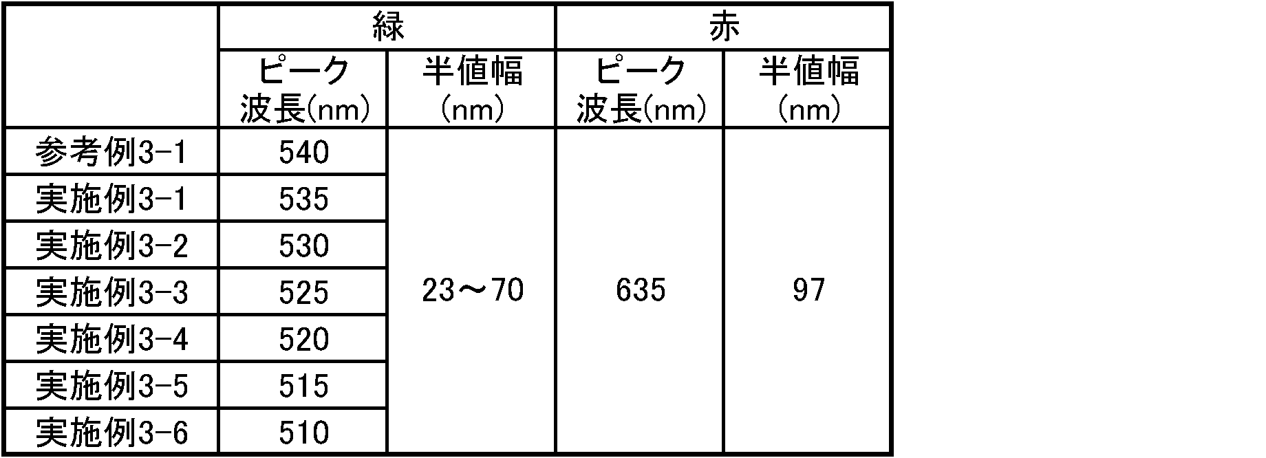
図10は、実施形態3における緑の半値幅(nm)と赤明度(%)との関係を示すグラフである。
実施形態3の構成は、バックライト光源のスペクトルの赤のピーク波長λpを645nmとする代わりに635nmとした以外は、実施形態1の構成と同様である。実施形態3においては、赤(R)のピーク波長λpが635nmのときに緑(G)のピーク波長を短くすること、例えば538nm以下とすることにより赤の明度を大きくすることが示されている。好ましくは、緑(G)のピーク波長を535nm以下とすることである。同じ緑のピーク波長の比較では、図10に示されるように、その半値幅が小さい程赤の明度向上の効果が大きくなる。
実施形態3の構成は、バックライト光源のスペクトルの赤のピーク波長λpを645nmとする代わりに635nmとした以外は、実施形態1の構成と同様である。実施形態3においては、赤(R)のピーク波長λpが635nmのときに緑(G)のピーク波長を短くすること、例えば538nm以下とすることにより赤の明度を大きくすることが示されている。好ましくは、緑(G)のピーク波長を535nm以下とすることである。同じ緑のピーク波長の比較では、図10に示されるように、その半値幅が小さい程赤の明度向上の効果が大きくなる。
図11は、実施形態3における緑の半値幅(nm)と青の彩度との関係を示すグラフである。図12は、実施形態3における緑の半値幅(nm)と黄の彩度との関係を示すグラフである。
緑(G)のピーク波長λpが低くなるほど、例えばλp<515nmとなる場合、赤明度はさらに高くなる。しかしながら、一方で、図11に示されるように青色表示の彩度の低下が発生し、また、図12に示されるように黄色表示の彩度の低下が発生する。従って、λp≧520nmとすることが好ましい。更に好ましくは、λp≧525nmとすることである。
緑(G)のピーク波長λpが低くなるほど、例えばλp<515nmとなる場合、赤明度はさらに高くなる。しかしながら、一方で、図11に示されるように青色表示の彩度の低下が発生し、また、図12に示されるように黄色表示の彩度の低下が発生する。従って、λp≧520nmとすることが好ましい。更に好ましくは、λp≧525nmとすることである。
上述した実施形態1~3より、赤のピーク波長によらず緑(G)のピーク波長を短くすることにより赤の明度を大きくすることができることが示されている。また、同じ緑のピーク波長の比較では、その半値幅が小さい程赤の明度向上の効果が大きくなることが示されている(図4、図7及び図10を参照)。
(実施形態4)
下記表6は、実施形態4(実施例4-1~実施例4-8)における緑のピーク波長(nm)、半値幅(nm)、赤のピーク波長(nm)、半値幅(それぞれ、10nm、15nm、20nm、40nm、60nm、80nm、100nm)を示す。
下記表6は、実施形態4(実施例4-1~実施例4-8)における緑のピーク波長(nm)、半値幅(nm)、赤のピーク波長(nm)、半値幅(それぞれ、10nm、15nm、20nm、40nm、60nm、80nm、100nm)を示す。

図13は、実施形態4における赤の半値幅(nm)と赤明度(%)との関係を示すグラフである。実施形態4では、開口比率がR:G:B:Y=1:1:1:1であり、表示面から射出される白の色温度10000K(x=0.278、y=0.291)の場合である。黄(Y)、青(B)の表示品位を劣化させない緑(G)のピーク波長535nm、半値幅58nmについて、さらに赤の明度を高くする赤(R)のピーク波長と半値幅を検討した。赤のピーク波長ごとに最も赤明度を高くする半値幅がある。
図14は、実施形態4において、縦軸を赤の半値幅(nm)、横軸を赤のピーク波長(nm)としたときの赤明度(%)を示す分布図である。
図15は、実施形態4における赤の半値幅(nm)と青の彩度との関係を示すグラフである。図16は、実施形態4における赤の半値幅(nm)と黄の彩度との関係を示すグラフである。実施形態4については、赤のピーク波長、半値幅による青の彩度、黄の彩度への影響は小さい。後述する実施形態5~9においては、赤の半値幅(nm)と青の彩度との関係を示すグラフ及び赤の半値幅(nm)と青の彩度との関係を示すグラフは示していないが、同様に青の彩度、黄の彩度への影響は小さい。なお、実施形態4において特に明示しない構成は、実施形態1に示した構成と同様である。
(実施形態5)
下記表7は、実施形態5(実施例5-1~実施例5-8)における緑のピーク波長(nm)、半値幅(nm)、赤のピーク波長(nm)、半値幅(それぞれ、10nm、15nm、20nm、40nm、60nm、80nm、100nm)を示す。
下記表7は、実施形態5(実施例5-1~実施例5-8)における緑のピーク波長(nm)、半値幅(nm)、赤のピーク波長(nm)、半値幅(それぞれ、10nm、15nm、20nm、40nm、60nm、80nm、100nm)を示す。
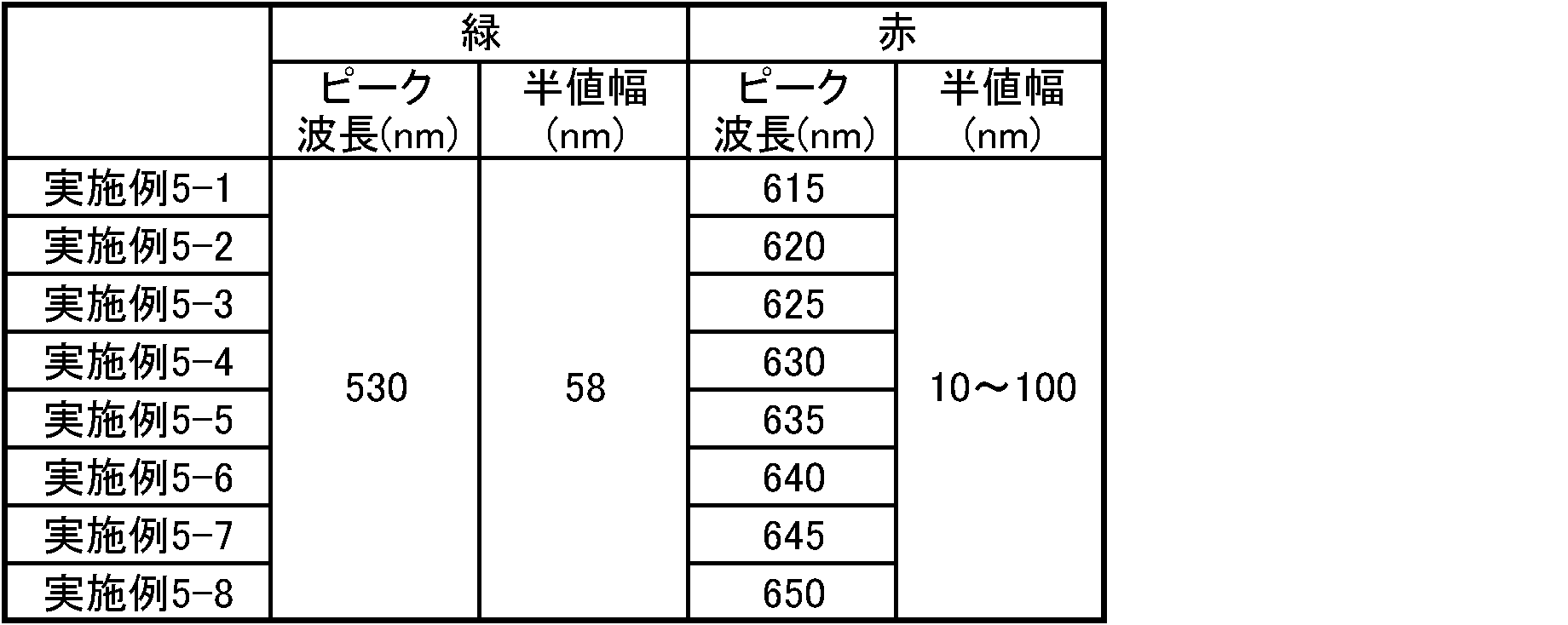
図17は、実施形態5における赤の半値幅(nm)と赤明度(%)との関係を示すグラフである。図18は、実施形態5において、縦軸を赤の半値幅(nm)、横軸を赤のピーク波長(nm)としたときの赤明度(%)を示す分布図である。実施形態5の構成は、バックライト光源のスペクトルの緑のピーク波長λpを535nmとする代わりに530nmとした以外は、実施形態4の構成と同様である。
(実施形態6)
下記表8は、実施形態6(実施例6-1~実施例6-8)における緑のピーク波長(nm)、半値幅(nm)、赤のピーク波長(nm)、半値幅(それぞれ、10nm、15nm、20nm、40nm、60nm、80nm、100nm)を示す。
下記表8は、実施形態6(実施例6-1~実施例6-8)における緑のピーク波長(nm)、半値幅(nm)、赤のピーク波長(nm)、半値幅(それぞれ、10nm、15nm、20nm、40nm、60nm、80nm、100nm)を示す。
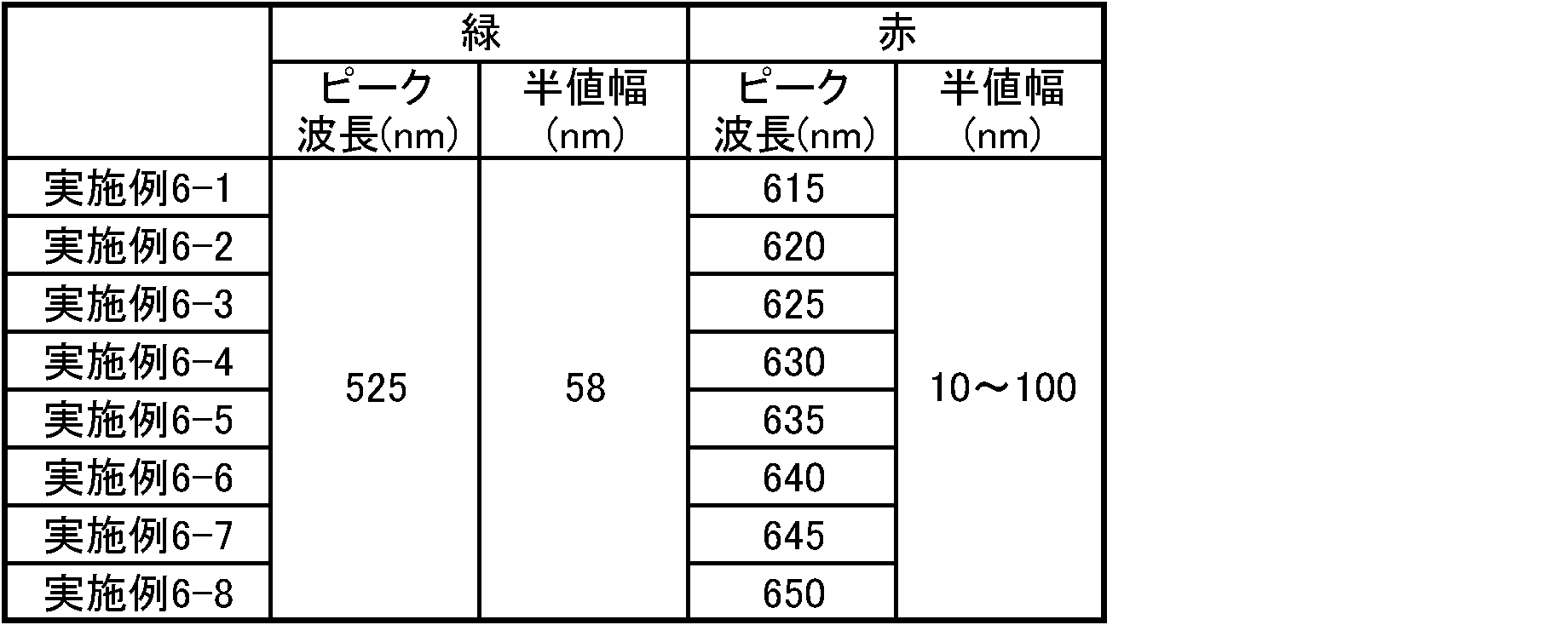
図19は、実施形態6における赤の半値幅(nm)と赤明度(%)との関係を示すグラフである。図20は、実施形態6において、縦軸を赤の半値幅(nm)、横軸を赤のピーク波長(nm)としたときの赤明度(%)を示す分布図である。
実施形態6の構成は、バックライト光源のスペクトルの緑のピーク波長λpを535nmとする代わりに525nmとした以外は、実施形態4の構成と同様である。
実施形態6の構成は、バックライト光源のスペクトルの緑のピーク波長λpを535nmとする代わりに525nmとした以外は、実施形態4の構成と同様である。
(実施形態7)
下記表9は、実施形態7(実施例7-1~実施例7-8)における緑のピーク波長(nm)、半値幅(nm)、赤のピーク波長(nm)、半値幅(それぞれ、10nm、15nm、20nm、40nm、60nm、80nm、100nm)を示す。
下記表9は、実施形態7(実施例7-1~実施例7-8)における緑のピーク波長(nm)、半値幅(nm)、赤のピーク波長(nm)、半値幅(それぞれ、10nm、15nm、20nm、40nm、60nm、80nm、100nm)を示す。
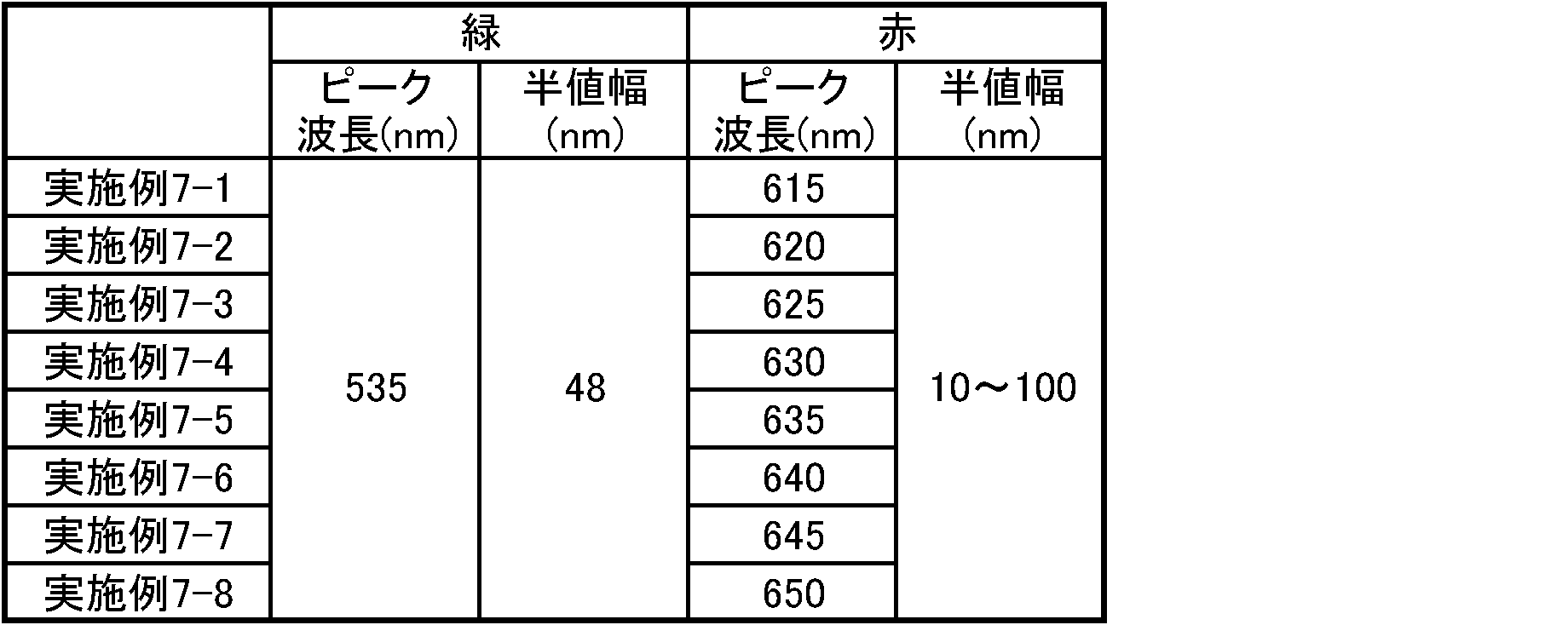
図21は、実施形態7における赤の半値幅(nm)と赤明度(%)との関係を示すグラフである。図22は、実施形態7において、縦軸を赤の半値幅(nm)、横軸を赤のピーク波長(nm)としたときの赤明度(%)を示す分布図である。
実施形態7の構成は、バックライト光源のスペクトルの緑の半値幅を58nmとする代わりに48nmとした以外は、実施形態4の構成と同様である。
実施形態7の構成は、バックライト光源のスペクトルの緑の半値幅を58nmとする代わりに48nmとした以外は、実施形態4の構成と同様である。
(実施形態8)
下記表10は、実施形態8(実施例8-1~実施例8-8)における緑のピーク波長(nm)、半値幅(nm)、赤のピーク波長(nm)、半値幅(それぞれ、10nm、15nm、20nm、40nm、60nm、80nm、100nm)を示す。
下記表10は、実施形態8(実施例8-1~実施例8-8)における緑のピーク波長(nm)、半値幅(nm)、赤のピーク波長(nm)、半値幅(それぞれ、10nm、15nm、20nm、40nm、60nm、80nm、100nm)を示す。

図23は、実施形態8における赤の半値幅(nm)と赤明度(%)との関係を示すグラフである。図24は、実施形態8において、縦軸を赤の半値幅(nm)、横軸を赤のピーク波長(nm)としたときの赤明度(%)を示す分布図である。
実施形態8の構成は、バックライト光源のスペクトルの緑の半値幅を58nmとする代わりに35nmとした以外は、実施形態4の構成と同様である。
実施形態8の構成は、バックライト光源のスペクトルの緑の半値幅を58nmとする代わりに35nmとした以外は、実施形態4の構成と同様である。
上述した実施形態4~実施形態8の結果から、以下のことが分かる。すなわち、実施例1-1~1-3の緑(G)(実施例2-1~2-3の緑(G)又は実施例3-1~3-3の緑(G)でもある。)について、赤(R)のピーク波長、半値幅を適切な構成とすることにより、赤明度が従来比110%以上と大幅に向上する。このように赤明度が110%以上となるように緑(G)のスペクトル形状とともに赤(R)のスペクトル形状を調整することが特に好ましい。例えば、光源から射出される緑(G)の光としては、510nm以上、535nm以下に緑色のピーク波長があるもの、光源から射出される光は、緑色の光として一般的な波長域である510nm以上、550nm以下に緑色のピーク波長があり、かつ緑色のピークの半値幅が57nm以下であるものとすることが好ましいが、中でも、緑(G)の光のピーク波長を525nm以上とすることが好ましい。また、緑(G)の光のピーク波長を540nm以下とすることが好ましい。更に、緑(G)の光の半値幅を50nm以下とすることが好ましい。より好ましくは、35nm以下である。更に、光源から射出される赤(R)の光としては、赤色のピーク波長が615nm以上、650nm以下にあることが好ましく、赤色のピークの半値幅は、10nm~100nmとすることが好ましい。更に、緑(G)の光のスペクトル形状(ピーク波長範囲、半値幅範囲)の好適な形態に、本発明の第1表示装置における好適な赤のスペクトル形状(ピーク波長範囲、半値幅範囲)を適用した形態が特に好適である。赤色のスペクトル形状と、緑色のスペクトル形状とを共に調整した表示装置が特に好ましく、本発明の効果を顕著に優れたものとすることができる。
(実施形態9)
下記表11は、実施形態9(実施例9-1~実施例9-8)における緑のピーク波長(nm)、半値幅(nm)、赤のピーク波長(nm)、半値幅(それぞれ、10nm、15nm、20nm、40nm、60nm、80nm、100nm)を示す。
下記表11は、実施形態9(実施例9-1~実施例9-8)における緑のピーク波長(nm)、半値幅(nm)、赤のピーク波長(nm)、半値幅(それぞれ、10nm、15nm、20nm、40nm、60nm、80nm、100nm)を示す。
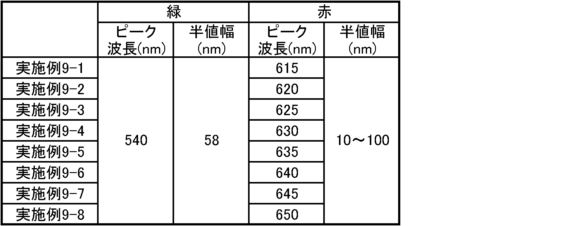
図25は、実施形態9における赤の半値幅(nm)と赤明度(%)との関係を示すグラフである。図26は、実施形態9において、縦軸を赤の半値幅(nm)、横軸を赤のピーク波長(nm)としたときの赤明度(%)を示す分布図である。
実施形態9の構成は、バックライト光源のスペクトルの緑のピーク波長λpを535nmとする代わりに540nmとした以外は、実施形態4の構成と同様である。
実施形態9の構成は、バックライト光源のスペクトルの緑のピーク波長λpを535nmとする代わりに540nmとした以外は、実施形態4の構成と同様である。
図25及び図26に示されるように、従来の緑(G)のスペクトルのままであっても、赤(R)のピーク波長、半値幅を適切な構成とすることにより、赤明度が従来比100%以上となる。
上述したように、赤の明度は、バックライトの緑(G)のスペクトル形状、赤(R)のスペクトル形状により異なる。更に、各画素の開口比率およびホワイトバランスの設定温度によっても異なる。赤の開口比率が大きくする、ホワイトバランスの色温度を低くすることにより、赤の明度が高くなる。上述した実施形態1~9では、開口比率は等しく、ホワイトバランスの色温度は10000Kの場合についての効果について説明した。実施形態1~9による赤の明度が高くなる効果は、他の開口比率、他のホワイトバランスの色温度の場合においても発揮できる。他の開口比率、ホワイトバランスの色温度で赤明度の効果を示す実施形態について、以下の実施形態10~14において詳述する。
(実施形態10)
下記表12は、実施形態10(実施例10-1~実施例10-8)における緑のピーク波長(nm)、半値幅(nm)、赤のピーク波長(nm)、半値幅(それぞれ、10nm、15nm、20nm、40nm、60nm、80nm、100nm)を示す。
下記表12は、実施形態10(実施例10-1~実施例10-8)における緑のピーク波長(nm)、半値幅(nm)、赤のピーク波長(nm)、半値幅(それぞれ、10nm、15nm、20nm、40nm、60nm、80nm、100nm)を示す。
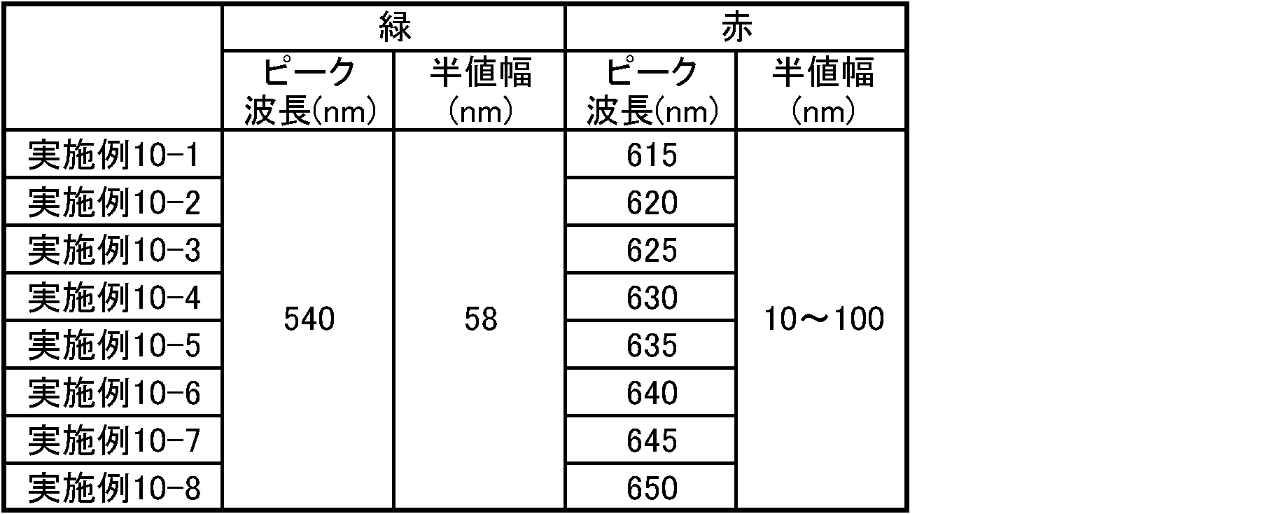
図27は、実施形態10における赤の半値幅(nm)と赤明度(%)との関係を示すグラフである。図28は、実施形態10において、縦軸を赤の半値幅(nm)、横軸を赤のピーク波長(nm)としたときの赤明度(%)を示す分布図である。
実施形態10の構成は、表示面から射出される白の色温度を10000K(x=0.278、y=0.291)とする代わりに9000K(x=0.285、y=0.299)とした以外は、実施形態9の構成と同様であり、赤の明度を高くする赤(R)のピーク波長と半値幅を検討したものである。
実施形態10の構成は、表示面から射出される白の色温度を10000K(x=0.278、y=0.291)とする代わりに9000K(x=0.285、y=0.299)とした以外は、実施形態9の構成と同様であり、赤の明度を高くする赤(R)のピーク波長と半値幅を検討したものである。
(実施形態11)
下記表13は、実施形態11(実施例11-1~実施例11-8)における緑のピーク波長(nm)、半値幅(nm)、赤のピーク波長(nm)、半値幅(それぞれ、10nm、15nm、20nm、40nm、60nm、80nm、100nm)を示す。
下記表13は、実施形態11(実施例11-1~実施例11-8)における緑のピーク波長(nm)、半値幅(nm)、赤のピーク波長(nm)、半値幅(それぞれ、10nm、15nm、20nm、40nm、60nm、80nm、100nm)を示す。

図29は、実施形態11における赤の半値幅(nm)と赤明度(%)との関係を示すグラフである。図30は、実施形態11において、縦軸を赤の半値幅(nm)、横軸を赤のピーク波長(nm)としたときの赤明度(%)を示す分布図である。
実施形態11の構成は、表示面から射出される白の色温度を10000K(x=0.278、y=0.291)とする代わりに8000K(x=0.294、y=0.309)とした以外は、実施形態9の構成と同様であり、赤の明度を高くする赤(R)のピーク波長と半値幅を検討したものである。
実施形態11の構成は、表示面から射出される白の色温度を10000K(x=0.278、y=0.291)とする代わりに8000K(x=0.294、y=0.309)とした以外は、実施形態9の構成と同様であり、赤の明度を高くする赤(R)のピーク波長と半値幅を検討したものである。
(実施形態12)
下記表14は、実施形態12(実施例12-1~実施例12-8)における緑のピーク波長(nm)、半値幅(nm)、赤のピーク波長(nm)、半値幅(それぞれ、10nm、15nm、20nm、40nm、60nm、80nm、100nm)を示す。
下記表14は、実施形態12(実施例12-1~実施例12-8)における緑のピーク波長(nm)、半値幅(nm)、赤のピーク波長(nm)、半値幅(それぞれ、10nm、15nm、20nm、40nm、60nm、80nm、100nm)を示す。

図31は、実施形態12における赤の半値幅(nm)と赤明度(%)との関係を示すグラフである。図32は、実施形態12において、縦軸を赤の半値幅(nm)、横軸を赤のピーク波長(nm)としたときの赤明度(%)を示す分布図である。
実施形態12の構成は、表示面から射出される白の色温度を10000K(x=0.278、y=0.291)とする代わりに6500K(x=0.313、y=0.329)とした以外は、実施形態9の構成と同様であり、赤の明度を高くする赤(R)のピーク波長と半値幅を検討したものである。
実施形態12の構成は、表示面から射出される白の色温度を10000K(x=0.278、y=0.291)とする代わりに6500K(x=0.313、y=0.329)とした以外は、実施形態9の構成と同様であり、赤の明度を高くする赤(R)のピーク波長と半値幅を検討したものである。
(実施形態13)
下記表15は、実施形態13(実施例13-1~実施例13-8)における緑のピーク波長(nm)、半値幅(nm)、赤のピーク波長(nm)、半値幅(それぞれ、10nm、15nm、20nm、40nm、60nm、80nm、100nm)を示す。
下記表15は、実施形態13(実施例13-1~実施例13-8)における緑のピーク波長(nm)、半値幅(nm)、赤のピーク波長(nm)、半値幅(それぞれ、10nm、15nm、20nm、40nm、60nm、80nm、100nm)を示す。

図33は、実施形態13の液晶表示装置における対向基板を模式的に示す平面図である。図34は、実施形態13の液晶表示装置を模式的に示す断面図である。
実施形態13の構成は、開口比率をR:G:B:Y=1:1:1:1とする代わりにR:G:B:Y=1.6:1:1.6:1とした以外は、実施形態9の構成と同様である。なお、図33及び図34において、図2及び図3に示したのと同様の機能を発揮する部材及び部分は、百の位に1を付した他は同じ符号を付している。
図35は、実施形態13における赤の半値幅(nm)と赤明度(%)との関係を示すグラフである。図36は、実施形態13において、縦軸を赤の半値幅(nm)、横軸を赤のピーク波長(nm)としたときの赤明度(%)を示す分布図である。
実施形態13は、開口比率がR:G:B:Y=1.6:1:1.6:1、表示面から射出される白の色温度10000K(x=0.278、y=0.291)の場合、従来のGreenのピーク波長540nm、半値幅が58nmについて、赤の明度を高くする赤(R)のピーク波長と半値幅を検討したものである。
実施形態13の構成は、開口比率をR:G:B:Y=1:1:1:1とする代わりにR:G:B:Y=1.6:1:1.6:1とした以外は、実施形態9の構成と同様である。なお、図33及び図34において、図2及び図3に示したのと同様の機能を発揮する部材及び部分は、百の位に1を付した他は同じ符号を付している。
図35は、実施形態13における赤の半値幅(nm)と赤明度(%)との関係を示すグラフである。図36は、実施形態13において、縦軸を赤の半値幅(nm)、横軸を赤のピーク波長(nm)としたときの赤明度(%)を示す分布図である。
実施形態13は、開口比率がR:G:B:Y=1.6:1:1.6:1、表示面から射出される白の色温度10000K(x=0.278、y=0.291)の場合、従来のGreenのピーク波長540nm、半値幅が58nmについて、赤の明度を高くする赤(R)のピーク波長と半値幅を検討したものである。
(実施形態14)
下記表16は、実施形態14(実施例14-1~実施例14-8)における緑のピーク波長(nm)、半値幅(nm)、赤のピーク波長(nm)、半値幅(それぞれ、10nm、15nm、20nm、40nm、60nm、80nm、100nm)を示す。
下記表16は、実施形態14(実施例14-1~実施例14-8)における緑のピーク波長(nm)、半値幅(nm)、赤のピーク波長(nm)、半値幅(それぞれ、10nm、15nm、20nm、40nm、60nm、80nm、100nm)を示す。
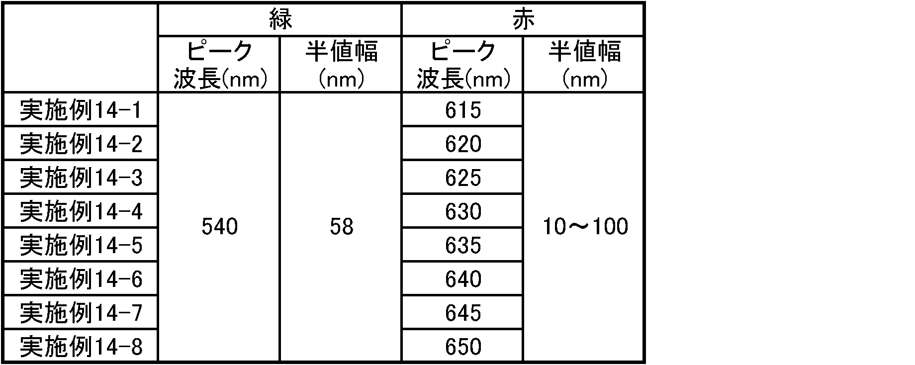
図37は、実施形態14の液晶表示装置における対向基板を模式的に示す平面図である。図38は、実施形態14の液晶表示装置を模式的に示す断面図である。
実施形態14の構成は、開口比率をR:G:B:Y=1:1:1:1とする代わりにR:G:B:Y=1.3:1:1.3:1とした以外は、実施形態9の構成と同様である。なお、図37及び図38において、図2及び図3に示したのと同様の機能を発揮する部材及び部分は、百の位に2を付した他は同じ符号を付している。
図39は、実施形態14における赤の半値幅(nm)と赤明度(%)との関係を示すグラフである。図40は、実施形態14において、縦軸を赤の半値幅(nm)、横軸を赤のピーク波長(nm)としたときの赤明度(%)を示す分布図である。
実施形態14は、開口比率がR:G:B:Y=1.3:1:1.3:1、白の色温度10000K(x=0.278、y=0.291)の場合、従来のGreenのピーク波長540nm、半値幅が58nmについて、赤の明度を高くする赤(R)のピーク波長と半値幅を検討したものである。
実施形態14の構成は、開口比率をR:G:B:Y=1:1:1:1とする代わりにR:G:B:Y=1.3:1:1.3:1とした以外は、実施形態9の構成と同様である。なお、図37及び図38において、図2及び図3に示したのと同様の機能を発揮する部材及び部分は、百の位に2を付した他は同じ符号を付している。
図39は、実施形態14における赤の半値幅(nm)と赤明度(%)との関係を示すグラフである。図40は、実施形態14において、縦軸を赤の半値幅(nm)、横軸を赤のピーク波長(nm)としたときの赤明度(%)を示す分布図である。
実施形態14は、開口比率がR:G:B:Y=1.3:1:1.3:1、白の色温度10000K(x=0.278、y=0.291)の場合、従来のGreenのピーク波長540nm、半値幅が58nmについて、赤の明度を高くする赤(R)のピーク波長と半値幅を検討したものである。
従来の緑(G)のスペクトルのままであっても、赤(R)のピーク波長、半値幅を適切な構成とすることにより赤明度が従来比100%以上となる等の本発明の効果を発揮することが出来る。例えば、上述したように、赤画素、緑画素、青画素、及び、黄画素を用いて画像が構成される表示装置であって、上記表示装置は、光源を備え、上記光源から射出される光は、615nm以上、650nm以下に赤色のピーク波長があり、上記赤色のピークの半値幅は、該ピーク波長が615nm以上、635nm以下である場合は、15nm以上、70nm以下であり、該ピーク波長が635nmを超え、640nm以下である場合は、40nm以上、93nm以下であり、該ピーク波長が640nmを超え、650nm以下である場合は、57nm以上、93nm以下である表示装置が好ましい。より好ましくは、上記赤色のピークの半値幅は、上記ピーク波長が615nm以上、625nm以下である場合は、15nm以上であり、上記ピーク波長が625nmを超え、635nm以下である場合は、30nm以上である表示装置である。これにより、赤明度を更に優れたものとすることが出来る。
また、実施形態9~12を比較すれば、表示面から射出される白の色温度を小さくするほど、赤明度の向上が得られることが分かる。
また、各画素の開口比を赤・青を緑・黄よりも大きくする程、赤明度の向上が得られる。
また、実施形態9~12を比較すれば、表示面から射出される白の色温度を小さくするほど、赤明度の向上が得られることが分かる。
また、各画素の開口比を赤・青を緑・黄よりも大きくする程、赤明度の向上が得られる。
実施形態9~実施形態14において、従来スペクトル(緑〔G〕のピーク波長540nm、半値幅58nmで赤〔R〕のピーク波長640nm、半値幅100nm)での赤明度は、それぞれ、100.0%(実施例9-6)・103.7%(実施例10-6)・109.1%(実施例11-6)・120.4%(実施例12-6)・131.4%(実施例13-6)・117.1%(実施例14-6)となる。この値を上回る実施形態については、本発明による効果がある。
(バックライトのスペクトル例)
図41は、実施例1-3で用いたバックライトのスペクトルを表す波長(nm)と強度との関係を示すグラフである。
なお、緑(G)、赤(R)のスペクトル形状は、以下の通りである。
緑(G):ピーク波長530nm、半値幅58nm
赤(R):ピーク波長640nm、半値幅100nm
図41は、実施例1-3で用いたバックライトのスペクトルを表す波長(nm)と強度との関係を示すグラフである。
なお、緑(G)、赤(R)のスペクトル形状は、以下の通りである。
緑(G):ピーク波長530nm、半値幅58nm
赤(R):ピーク波長640nm、半値幅100nm
図42は、実施例5-4で用いたバックライトのスペクトルを表す波長(nm)と強度との関係を示すグラフである。
なお、緑(G)、赤(R)のスペクトル形状は、以下の通りである。
緑(G):ピーク波長530nm、半値幅58nm
赤(R):ピーク波長640nm、半値幅58nm
なお、緑(G)、赤(R)のスペクトル形状は、以下の通りである。
緑(G):ピーク波長530nm、半値幅58nm
赤(R):ピーク波長640nm、半値幅58nm
図43は、参考例1-1で用いたバックライトのスペクトルを表す波長(nm)と強度との関係を示すグラフである。
なお、緑(G)、赤(R)のスペクトル形状は、以下の通りである。
緑(G):ピーク波長540nm、半値幅58nm
赤(R):ピーク波長640nm、半値幅100nm
なお、緑(G)、赤(R)のスペクトル形状は、以下の通りである。
緑(G):ピーク波長540nm、半値幅58nm
赤(R):ピーク波長640nm、半値幅100nm
補足すれば、バックライトのスペクトルの放射強度において最大の強度を持つ波長、二番目の強度を持つ波長、三番目の強度を持つ波長の3つの波長が、大まかには例えば400nm~500nm、500nm~600nm、600nm~700nmのように青、緑、赤に対応する3つの領域に分かれる。青のピーク波長は440nm~460nmであり、青の半値幅は小さいほうが良く30nm以下が好ましい。
青、黄の彩度(C*)は、CIE1976において定義される通り、{(a*)2+(b*)2}0.5で表される。なお、a*及びb*は、色度図における色の方向を示し、a*は赤方向、b*は黄方向を示す。青の彩度は25以上、黄の彩度は40以上であれば表示品は良好である。
(計算方法について)
本実施形態のピーク波長等に関する計算方法について、以下に説明する。
バックライトのスペクトルとしては、BL1(λ)及びBL2(λ)を考える。以下に詳述する。
本明細書中、バックライトのスペクトルは、RGBの各波長域の発光体単体のスペクトル分布がピーク波長を中心にガウス分布しているとし、それぞれを合成したものとする。
本実施形態のピーク波長等に関する計算方法について、以下に説明する。
バックライトのスペクトルとしては、BL1(λ)及びBL2(λ)を考える。以下に詳述する。
本明細書中、バックライトのスペクトルは、RGBの各波長域の発光体単体のスペクトル分布がピーク波長を中心にガウス分布しているとし、それぞれを合成したものとする。
液晶層の各色表示の分光透過率特性を以下のように表す。すなわち、液晶層の白表示の分光透過率特性をLCDw(λ)とし、液晶層の黒表示の分光透過率特性をLCDbk(λ)とする。また、赤カラーフィルタの分光透過率特性をCFr(λ)とし、緑カラーフィルタの分光透過率特性をCFg(λ)とし、青カラーフィルタの分光透過率特性をCFb(λ)とし、黄カラーフィルタの分光透過率特性をCFy(λ)とし、シアンカラーフィルタの分光透過率特性をCFc(λ)とする。
また各色画素の開口比を以下のように表す。すなわち、赤画素の開口比をPrとし、緑画素の開口比をPgとし、青画素の開口比をPbとし、黄画素の開口比をPyとし、シアン画素の開口比をPcとする。Pr+Pg+Pb+Py+Pc=1とし、表示装置がシアン画素を含まない場合はPc=0とする。
まず、任意のバックライトのスペクトルBL1(λ)を使用した表示装置の白表示のスペクトルは、下記式1により得られる。
White(λ)={Pr・CFr(λ)・LCDw(λ)+Pg・CFg(λ)・LCDw(λ)+Pb・CFb(λ)・LCDw(λ)+Py・CFy(λ)・LCDw(λ)+Pc・CFc(λ)・LCDbk(λ)}×BL1(λ) (式1)
この白表示の色度(xw,yw)は、CIE表色系にもとづき、(式1)により得られた白表示の波長特性White(λ)から白表示の三刺激値Xw、Yw、Zwを算出し、このXw、Yw、Zwを用いて白表示の色度(xw,yw)を得る。
White(λ)={Pr・CFr(λ)・LCDw(λ)+Pg・CFg(λ)・LCDw(λ)+Pb・CFb(λ)・LCDw(λ)+Py・CFy(λ)・LCDw(λ)+Pc・CFc(λ)・LCDbk(λ)}×BL1(λ) (式1)
この白表示の色度(xw,yw)は、CIE表色系にもとづき、(式1)により得られた白表示の波長特性White(λ)から白表示の三刺激値Xw、Yw、Zwを算出し、このXw、Yw、Zwを用いて白表示の色度(xw,yw)を得る。
ここで求めた色度(xw,yw)が所定の色度にならない場合には、バックライトのR領域、G領域のピークの高さを変化させることにより白表示の色度が所定の値となるように調整する。この調整後のバックライトのスペクトルをBL2(λ)とする。
また、他の表示色は、白表示の色度調整後のバックライトのスペクトルBL2(λ)を用いて、下記(式2)~(式6)により算出する。
Red(λ)={Pr・CFr(λ)・LCDw(λ)+Pg・CFg(λ)・LCDbk(λ)+Pb・CFb(λ)・LCDbk(λ)+Py・CFy(λ)・LCDbk(λ)+Pc・CFc(λ)・LCDbk(λ)}×BL2(λ) (式2)
Green(λ)={Pr・CFr(λ)・LCDbk(λ)+Pg・CFg(λ)・LCDw(λ)+Pb・CFb(λ)・LCDbk(λ)+Py・CFy(λ)・LCDbk(λ)+Pc・CFc(λ)・LCDbk(λ)}×BL2(λ) (式3)
Blue(λ)={Pr・CFr(λ)・LCDbk(λ)+Pg・CFg(λ)・LCDbk(λ)+Pb・CFb(λ)・LCDw(λ)+Py・CFy(λ)・LCDbk(λ)+Pc・CFc(λ)・LCDbk(λ)}×BL2(λ) (式4)
Yellow(λ)={Pr・CFr(λ)・LCDw(λ)+Pg・CFg(λ)・LCDw(λ)+Pb・CFb(λ)・LCDbk(λ)+Py・CFy(λ)・LCDw(λ)+Pc・CFc(λ)・LCDbk(λ)}×BL2(λ) (式5)
Cyan(λ)={Pr・CFr(λ)・LCDbk(λ)+Pg・CFg(λ)・LCDbk(λ)+Pb・CFb(λ)・LCDbk(λ)+Py・CFy(λ)・LCDbk(λ)+Pc・CFc(λ)・LCDw(λ)}×BL2(λ) (式6)
以上より得られる各表示色のスペクトルから、上述の白表示の場合と同様に各表示色の三刺激値を算出し、CIE表色系にもとづき色度、明度、彩度を算出する。なお、赤の表示色の色度座標xがBL2(λ)によっては0.64未満となる場合がある。この場合は、赤の表示色の色度座標xが0.64以上となるようにCFr(λ)を再調整した。
また、他の表示色は、白表示の色度調整後のバックライトのスペクトルBL2(λ)を用いて、下記(式2)~(式6)により算出する。
Red(λ)={Pr・CFr(λ)・LCDw(λ)+Pg・CFg(λ)・LCDbk(λ)+Pb・CFb(λ)・LCDbk(λ)+Py・CFy(λ)・LCDbk(λ)+Pc・CFc(λ)・LCDbk(λ)}×BL2(λ) (式2)
Green(λ)={Pr・CFr(λ)・LCDbk(λ)+Pg・CFg(λ)・LCDw(λ)+Pb・CFb(λ)・LCDbk(λ)+Py・CFy(λ)・LCDbk(λ)+Pc・CFc(λ)・LCDbk(λ)}×BL2(λ) (式3)
Blue(λ)={Pr・CFr(λ)・LCDbk(λ)+Pg・CFg(λ)・LCDbk(λ)+Pb・CFb(λ)・LCDw(λ)+Py・CFy(λ)・LCDbk(λ)+Pc・CFc(λ)・LCDbk(λ)}×BL2(λ) (式4)
Yellow(λ)={Pr・CFr(λ)・LCDw(λ)+Pg・CFg(λ)・LCDw(λ)+Pb・CFb(λ)・LCDbk(λ)+Py・CFy(λ)・LCDw(λ)+Pc・CFc(λ)・LCDbk(λ)}×BL2(λ) (式5)
Cyan(λ)={Pr・CFr(λ)・LCDbk(λ)+Pg・CFg(λ)・LCDbk(λ)+Pb・CFb(λ)・LCDbk(λ)+Py・CFy(λ)・LCDbk(λ)+Pc・CFc(λ)・LCDw(λ)}×BL2(λ) (式6)
以上より得られる各表示色のスペクトルから、上述の白表示の場合と同様に各表示色の三刺激値を算出し、CIE表色系にもとづき色度、明度、彩度を算出する。なお、赤の表示色の色度座標xがBL2(λ)によっては0.64未満となる場合がある。この場合は、赤の表示色の色度座標xが0.64以上となるようにCFr(λ)を再調整した。
補足すれば、LED発光タイプの緑(G)のピーク波長は530nm、半値幅32nmである。赤(R)のピーク波長は630nm、半値幅17nmである。現状使用されている蛍光発光タイプの緑(G)のピーク波長は539nm、半値幅59nmである。赤(R)のピーク波長は638nm、半値幅97nmである。
なお、工業的な製造においては、実際にはLED発光タイプのバックライト、蛍光発光のバックライトのいずれもが個体差によりピーク波長、半値幅とも±3nm程度のばらつきが発生する場合がある。
なお、工業的な製造においては、実際にはLED発光タイプのバックライト、蛍光発光のバックライトのいずれもが個体差によりピーク波長、半値幅とも±3nm程度のばらつきが発生する場合がある。
実施形態1~14では、バックライトの光源としては、冷陰極蛍光管(CCFT、CCFL)、白の発光ダイオード(青発光LEDと黄蛍光発光との組み合わせ)やRGB-LEDや、熱陰極蛍光管(HCFT)や有機EL、電界放出ディスプレイ(FED)等を適宜用いることができる。
また実施形態1~14では、バックライトを用いて表示を行う透過型の液晶表示装置についての説明であったが、本発明は、透過型の液晶表示装置だけでなく、バックライトを用いて透過表示を行い、外部光及び/又はフロントライトを用いて反射表示を行う反射透過両用型の液晶表示装置、フロントライト等の光源を用いて表示を行う反射型の液晶表示装置等、他の表示方式の液晶表示装置、ブラウン管(CRT)、有機エレクトロルミネセンス表示装置(OELD)、プラズマディスプレイパネル(PDP)、及び、表面伝導型電子放出素子ディスプレイ(SED)等の電界放出ディスプレイ(FED)等、種々の表示装置に好適に用いられるものである。なお、本願明細書における「以上」及び「以下」は、当該数値(境界値)を含むものである。
上述した実施形態における各形態は、本発明の要旨を逸脱しない範囲において適宜組み合わされてもよい。
なお、本願は、2011年6月7日に出願された日本国特許出願2011-127603号を基礎として、パリ条約ないし移行する国における法規に基づく優先権を主張するものである。該出願の内容は、その全体が本願中に参照として組み込まれている。
3:補助容量
4:走査線
6:信号線
7:補助容量(Cs)配線
8:薄膜トランジスタ(TFT)
9:ドレイン引出し配線
10R、110R、210R:赤のカラーフィルタ
10G、110G、210G:緑のカラーフィルタ
10B、110B、210B:青のカラーフィルタ
10Y、110Y、210Y:黄のカラーフィルタ
10BM、110BM、210BM:ブラックマトリクス(黒塗りされた部分)
20、120、220: カラーフィルタ基板(対向基板)
21、31、121、131、221、231:ガラス基板
22、32、122、132、222、232:位相差板
23、33、123、133、223、233:偏光板
25、125、225:オーバーコート層
26、126、226:対向電極
27、38、127、138、227、238:配向膜
30、130、230:薄膜トランジスタ(TFT)基板
34、134、234:層間絶縁膜
35、135、235:透明電極
35R、135R、235R:赤の透明電極
35G、135G、235G:緑の透明電極
35B、135B、235B:青の透明電極
35Y、135Y、235Y:黄の透明電極
36、136、236:バックライト
37、137、237:コンタクトホール
40、140、240:液晶層
50、150、250:液晶表示装置
4:走査線
6:信号線
7:補助容量(Cs)配線
8:薄膜トランジスタ(TFT)
9:ドレイン引出し配線
10R、110R、210R:赤のカラーフィルタ
10G、110G、210G:緑のカラーフィルタ
10B、110B、210B:青のカラーフィルタ
10Y、110Y、210Y:黄のカラーフィルタ
10BM、110BM、210BM:ブラックマトリクス(黒塗りされた部分)
20、120、220: カラーフィルタ基板(対向基板)
21、31、121、131、221、231:ガラス基板
22、32、122、132、222、232:位相差板
23、33、123、133、223、233:偏光板
25、125、225:オーバーコート層
26、126、226:対向電極
27、38、127、138、227、238:配向膜
30、130、230:薄膜トランジスタ(TFT)基板
34、134、234:層間絶縁膜
35、135、235:透明電極
35R、135R、235R:赤の透明電極
35G、135G、235G:緑の透明電極
35B、135B、235B:青の透明電極
35Y、135Y、235Y:黄の透明電極
36、136、236:バックライト
37、137、237:コンタクトホール
40、140、240:液晶層
50、150、250:液晶表示装置
Claims (10)
- 赤画素、緑画素、青画素、及び、黄画素を用いて画像が構成される表示装置であって、
該表示装置は、光源を備え、
該光源から射出される光は、615nm以上、650nm以下に赤色のピーク波長があり、
該赤色のピークの半値幅は、該ピーク波長が615nm以上、635nm以下である場合は、15nm以上、70nm以下であり、該ピーク波長が635nmを超え、640nm以下である場合は、40nm以上、93nm以下であり、該ピーク波長が640nmを超え、650nm以下である場合は、57nm以上、93nm以下である
ことを特徴とする表示装置。 - 前記赤色のピーク波長は、635nm以下である
ことを特徴とする請求項1に記載の表示装置。 - 赤画素、緑画素、青画素、及び、黄画素を用いて画像が構成される表示装置であって、
該表示装置は、光源を備え、
該光源から射出される光は、510nm以上、535nm以下に緑色のピーク波長がある
ことを特徴とする表示装置。 - 前記緑色のピーク波長は、520nm以上である
ことを特徴とする請求項3に記載の表示装置。 - 赤画素、緑画素、青画素、及び、黄画素を用いて画像が構成される表示装置であって、
該表示装置は、光源を備え、
該光源から射出される光は、510nm以上、540nm以下に緑色のピーク波長があり、
該緑色のピークの半値幅は、57nm以下である
ことを特徴とする表示装置。 - 前記緑色のピークの半値幅は、30nm以上である
ことを特徴とする請求項5に記載の表示装置。 - 前記表示装置の各色間の画素面積比が1以上、1.6以下である
ことを特徴とする請求項1~6のいずれかに記載の表示装置。 - 前記表示装置は、少なくとも赤色のカラーフィルタ、緑色のカラーフィルタ、青色のカラーフィルタ、及び、黄色のカラーフィルタが画素毎に配置されたカラーフィルタ基板を備える
ことを特徴とする請求項1~7のいずれかに記載の表示装置。 - 前記表示装置は、液晶表示装置である
ことを特徴とする請求項1~8のいずれかに記載の表示装置。 - 前記表示装置は、表示面から射出される白色光の色温度が12000K未満であることを特徴とする請求項1~9のいずれかに記載の表示装置。
Priority Applications (1)
| Application Number | Priority Date | Filing Date | Title |
|---|---|---|---|
| US14/123,804 US20140111748A1 (en) | 2011-06-07 | 2012-05-31 | Display device |
Applications Claiming Priority (2)
| Application Number | Priority Date | Filing Date | Title |
|---|---|---|---|
| JP2011-127603 | 2011-06-07 | ||
| JP2011127603 | 2011-06-07 |
Publications (1)
| Publication Number | Publication Date |
|---|---|
| WO2012169421A1 true WO2012169421A1 (ja) | 2012-12-13 |
Family
ID=47295987
Family Applications (1)
| Application Number | Title | Priority Date | Filing Date |
|---|---|---|---|
| PCT/JP2012/064082 Ceased WO2012169421A1 (ja) | 2011-06-07 | 2012-05-31 | 表示装置 |
Country Status (2)
| Country | Link |
|---|---|
| US (1) | US20140111748A1 (ja) |
| WO (1) | WO2012169421A1 (ja) |
Cited By (1)
| Publication number | Priority date | Publication date | Assignee | Title |
|---|---|---|---|---|
| WO2016063812A1 (ja) * | 2014-10-24 | 2016-04-28 | シャープ株式会社 | 表示装置 |
Families Citing this family (3)
| Publication number | Priority date | Publication date | Assignee | Title |
|---|---|---|---|---|
| JP6013067B2 (ja) * | 2012-07-26 | 2016-10-25 | 株式会社ジャパンディスプレイ | 表示装置及びその製造方法 |
| JP2015037062A (ja) * | 2013-08-15 | 2015-02-23 | ソニー株式会社 | 表示装置及び電子機器 |
| KR102649299B1 (ko) * | 2018-03-09 | 2024-03-19 | 삼성전자주식회사 | 전계발광 표시 장치 |
Citations (3)
| Publication number | Priority date | Publication date | Assignee | Title |
|---|---|---|---|---|
| JP2006106437A (ja) * | 2004-10-06 | 2006-04-20 | Sony Corp | カラー液晶表示装置 |
| WO2006068141A1 (ja) * | 2004-12-24 | 2006-06-29 | Kabushiki Kaisha Toshiba | 白色ledおよびそれを用いたバックライト並びに液晶表示装置 |
| WO2007148519A1 (ja) * | 2006-06-19 | 2007-12-27 | Sharp Kabushiki Kaisha | 表示装置 |
Family Cites Families (5)
| Publication number | Priority date | Publication date | Assignee | Title |
|---|---|---|---|---|
| JPWO2006019016A1 (ja) * | 2004-08-18 | 2008-05-08 | ソニー株式会社 | バックライト装置及びカラー液晶表示装置 |
| US7439670B2 (en) * | 2005-02-03 | 2008-10-21 | Eastman Kodak Company | Making multicolor OLED displays |
| JP2007317591A (ja) * | 2006-05-29 | 2007-12-06 | Seiko Epson Corp | 有機el発光装置および電子機器 |
| KR100932978B1 (ko) * | 2007-11-28 | 2009-12-21 | 삼성에스디아이 주식회사 | 백색 형광체, 이를 이용하는 발광 장치, 및 이 발광 장치를백 라이트 유닛으로 사용하는 액정 표시 장치 |
| KR101735812B1 (ko) * | 2010-09-10 | 2017-05-16 | 삼성디스플레이 주식회사 | 표시장치 |
-
2012
- 2012-05-31 WO PCT/JP2012/064082 patent/WO2012169421A1/ja not_active Ceased
- 2012-05-31 US US14/123,804 patent/US20140111748A1/en not_active Abandoned
Patent Citations (3)
| Publication number | Priority date | Publication date | Assignee | Title |
|---|---|---|---|---|
| JP2006106437A (ja) * | 2004-10-06 | 2006-04-20 | Sony Corp | カラー液晶表示装置 |
| WO2006068141A1 (ja) * | 2004-12-24 | 2006-06-29 | Kabushiki Kaisha Toshiba | 白色ledおよびそれを用いたバックライト並びに液晶表示装置 |
| WO2007148519A1 (ja) * | 2006-06-19 | 2007-12-27 | Sharp Kabushiki Kaisha | 表示装置 |
Cited By (1)
| Publication number | Priority date | Publication date | Assignee | Title |
|---|---|---|---|---|
| WO2016063812A1 (ja) * | 2014-10-24 | 2016-04-28 | シャープ株式会社 | 表示装置 |
Also Published As
| Publication number | Publication date |
|---|---|
| US20140111748A1 (en) | 2014-04-24 |
Similar Documents
| Publication | Publication Date | Title |
|---|---|---|
| JP5284513B2 (ja) | 表示装置 | |
| JP5172656B2 (ja) | 表示装置 | |
| CN100442113C (zh) | 液晶显示器 | |
| US8605238B2 (en) | Image display apparatus | |
| CN114488610B (zh) | 显示面板及显示装置 | |
| CN101636775B (zh) | 显示装置 | |
| CN102597859A (zh) | 液晶显示装置 | |
| WO2012169421A1 (ja) | 表示装置 | |
| US9213197B2 (en) | Color filter substrate, liquid crystal panel and liquid crystal display | |
| US20130258258A1 (en) | Liquid crystal display device | |
| CN101256304A (zh) | 具有高色彩饱和度的显示器模块 | |
| KR20120076256A (ko) | 액정표시장치 | |
| KR101768232B1 (ko) | 액정표시장치 | |
| KR20150078345A (ko) | 액정표시장치 | |
| JP2007226084A (ja) | 表示装置とカラーフィルタ及びそれらを備えた液晶表示装置、液晶表示装置用パネルと電子機器 |
Legal Events
| Date | Code | Title | Description |
|---|---|---|---|
| 121 | Ep: the epo has been informed by wipo that ep was designated in this application |
Ref document number: 12797661 Country of ref document: EP Kind code of ref document: A1 |
|
| WWE | Wipo information: entry into national phase |
Ref document number: 14123804 Country of ref document: US |
|
| NENP | Non-entry into the national phase |
Ref country code: DE |
|
| 122 | Ep: pct application non-entry in european phase |
Ref document number: 12797661 Country of ref document: EP Kind code of ref document: A1 |
|
| NENP | Non-entry into the national phase |
Ref country code: JP |