WO2012169032A1 - バッファ装置,バッファ制御装置,及びバッファ制御方法 - Google Patents
バッファ装置,バッファ制御装置,及びバッファ制御方法 Download PDFInfo
- Publication number
- WO2012169032A1 WO2012169032A1 PCT/JP2011/063214 JP2011063214W WO2012169032A1 WO 2012169032 A1 WO2012169032 A1 WO 2012169032A1 JP 2011063214 W JP2011063214 W JP 2011063214W WO 2012169032 A1 WO2012169032 A1 WO 2012169032A1
- Authority
- WO
- WIPO (PCT)
- Prior art keywords
- buffer
- input
- pointer
- read
- information
- Prior art date
- Legal status (The legal status is an assumption and is not a legal conclusion. Google has not performed a legal analysis and makes no representation as to the accuracy of the status listed.)
- Ceased
Links
Images









Classifications
-
- G—PHYSICS
- G06—COMPUTING OR CALCULATING; COUNTING
- G06F—ELECTRIC DIGITAL DATA PROCESSING
- G06F3/00—Input arrangements for transferring data to be processed into a form capable of being handled by the computer; Output arrangements for transferring data from processing unit to output unit, e.g. interface arrangements
- G06F3/06—Digital input from, or digital output to, record carriers, e.g. RAID, emulated record carriers or networked record carriers
- G06F3/0601—Interfaces specially adapted for storage systems
- G06F3/0628—Interfaces specially adapted for storage systems making use of a particular technique
- G06F3/0655—Vertical data movement, i.e. input-output transfer; data movement between one or more hosts and one or more storage devices
- G06F3/0656—Data buffering arrangements
-
- G—PHYSICS
- G06—COMPUTING OR CALCULATING; COUNTING
- G06F—ELECTRIC DIGITAL DATA PROCESSING
- G06F5/00—Methods or arrangements for data conversion without changing the order or content of the data handled
- G06F5/06—Methods or arrangements for data conversion without changing the order or content of the data handled for changing the speed of data flow, i.e. speed regularising or timing, e.g. delay lines, FIFO buffers; over- or underrun control therefor
- G06F5/065—Partitioned buffers, e.g. allowing multiple independent queues, bidirectional FIFO's
-
- G—PHYSICS
- G06—COMPUTING OR CALCULATING; COUNTING
- G06F—ELECTRIC DIGITAL DATA PROCESSING
- G06F3/00—Input arrangements for transferring data to be processed into a form capable of being handled by the computer; Output arrangements for transferring data from processing unit to output unit, e.g. interface arrangements
- G06F3/06—Digital input from, or digital output to, record carriers, e.g. RAID, emulated record carriers or networked record carriers
- G06F3/0601—Interfaces specially adapted for storage systems
- G06F3/0602—Interfaces specially adapted for storage systems specifically adapted to achieve a particular effect
- G06F3/061—Improving I/O performance
-
- G—PHYSICS
- G06—COMPUTING OR CALCULATING; COUNTING
- G06F—ELECTRIC DIGITAL DATA PROCESSING
- G06F3/00—Input arrangements for transferring data to be processed into a form capable of being handled by the computer; Output arrangements for transferring data from processing unit to output unit, e.g. interface arrangements
- G06F3/06—Digital input from, or digital output to, record carriers, e.g. RAID, emulated record carriers or networked record carriers
- G06F3/0601—Interfaces specially adapted for storage systems
- G06F3/0668—Interfaces specially adapted for storage systems adopting a particular infrastructure
- G06F3/0671—In-line storage system
- G06F3/0683—Plurality of storage devices
-
- G—PHYSICS
- G06—COMPUTING OR CALCULATING; COUNTING
- G06F—ELECTRIC DIGITAL DATA PROCESSING
- G06F5/00—Methods or arrangements for data conversion without changing the order or content of the data handled
- G06F5/06—Methods or arrangements for data conversion without changing the order or content of the data handled for changing the speed of data flow, i.e. speed regularising or timing, e.g. delay lines, FIFO buffers; over- or underrun control therefor
- G06F5/16—Multiplexed systems, i.e. using two or more similar devices which are alternately accessed for enqueue and dequeue operations, e.g. ping-pong buffers
Definitions
- This case relates to a buffer device, a buffer control device, and a buffer control method in an information processing system.
- FIG. 16 is a diagram illustrating a configuration example of the buffer device 200 corresponding to a plurality of inputs and one output.
- FIGS. 17 and 18 are information processing systems 100-1 and 100-2 including the buffer device 200 illustrated in FIG. FIG.
- a buffer device 200 corresponding to three inputs and one output is shown.
- the direction of the arrow in FIGS. 17 and 18 indicates the data transmission direction.
- the buffer device 200 includes buffers 500-1 to 500-3 in parallel for the input ports 300-1 to 300-3, and each buffer 500 includes a corresponding input port 300-1 to 300-1.
- the data input from 300-3 via the input paths 300A to 300C is stored.
- the buffers 500-1 to 500-3 are not distinguished, they are simply referred to as the buffer 500.
- Examples of the buffer 500 include a volatile memory such as a RAM (Random Access Memory).
- the buffer device 200 selects data to be output from the output target buffer 500 based on the arbitration result by the arbitration unit 660 and outputs the selected data to the output path 700A. That is, the data read from the output target buffer 500 is output from the output port 700.
- the buffer device 200 includes write control pointers 500a-1 to 500a-3 and read control pointers 500b-1 to 500b-3 corresponding to the buffers 500, respectively.
- the write control pointers 500a-1 to 500a-3 and the read control pointers 500b-1 to 500b-3 are not distinguished, they are simply referred to as the write control pointer 500a and the read control pointer 500b, respectively.
- the write control pointer 500a and the read control pointer 500b are denoted as WP and RP in FIG. 16, respectively.
- the write address of the buffer 500 is recorded as a pointer value, and the input data to the buffer 500 is written at the address position indicated by the pointer value of the corresponding write control pointer 500a.
- the write control pointer 500a increments the corresponding pointer value every time input data is written to the corresponding buffer 500.
- the read address of the output data from the buffer 500 is recorded as a pointer value, and the data stored in the buffer 500 is read from the address position indicated by the pointer value of the corresponding read control pointer 500b. .
- the read control pointer 500b increments its own pointer value every time output data is read from the corresponding buffer 500.
- the arbitration unit 660 adjusts the read timing of data from the buffer 500 and selects (arbitrates) the buffer 500 to be read.
- the arbitration unit 660 outputs a control signal that causes the selector 630 to select the buffer 500 to be read as an arbitration result at each read timing. Note that the arbitration unit 660 selects the buffer 500 to be read using, for example, an LRU (Least Recently Used) method or a round robin method.
- LRU Least Recently Used
- the selector 630 reads output data from the address position indicated by the pointer value of the read control pointer 500b corresponding to the buffer 500 to be read based on the arbitration result by the arbitration unit 660, and outputs it to the output path 700A.
- the input ports 300-1 to 300-3 and the output port 700 are connected to, for example, an information processing apparatus such as a server, a system board (SB), and the like.
- a buffer device 200 shown in FIG. 16 is provided for a crossbar chip (XB; Cross Bar: hereinafter referred to as XB) or the like in the information processing system 100-1 shown in FIG. 17 or the information processing system 100-2 shown in FIG. It is done.
- buffer devices 200-1 to 200-4 respectively corresponding to the buffer device 200 are provided in the XB 120.
- the output side of each of the buffer devices 200-1 to 200-4, that is, the output port 700 is connected to the corresponding SB 110-1 to 110-4, and the input side of each of the buffer devices 200-1 to 200-4, that is,
- the input ports 300-1 to 300-3 are connected to SBs 110-1 to 110-4 other than the corresponding SB, respectively.
- the SBs 110-1 to 110-4 are connected to each other via the XB 120 so that they can communicate with each other.
- An information processing system 100-2 illustrated in FIG. 18 includes XBs 120-1 and 120-2 that are communicably connected to each other via a long-distance transmission path.
- the XB 120-1 includes SBs 110-1 to 110-3 that are communicatively connected to each other, and the XB 120-2 includes SBs 110-4 to 110-6 that are communicatively connected to each other.
- the XB 120-2 includes buffer devices 200-1 to 200-4 respectively corresponding to the buffer device 200, like the XB 120 shown in FIG.
- the XB 120-1 has the same configuration as the XB 120-2 and the XB 120 shown in FIG.
- the output side of the buffer device 200-1 in the XB 120-2 is connected to the XB 120-1 via a long-distance transmission path, and the output side of each of the buffer devices 200-2 to 200-4 is Are connected to the corresponding SBs 110-4 to 110-6.
- the input side of the buffer device 200-1 in the XB 120-2 is connected to each of the SBs 110-4 to 110-6.
- the input side of each of the buffer devices 200-2 to 200-4 in the XB 120-2 is connected to the XB 120-1 via a SB 110-4 to 110-6 other than the corresponding SB and a long distance transmission path. .
- the SBs 110-1 to 110-3 and the SBs 110-4 to 110-6 are XB 120-1, long-distance transmission paths. , And XB 120-2 so that they can communicate with each other.
- an empty FIFO queue for storing empty FIFO (First In, First Out) numbers is provided, and when the FIFO indicated by the write pointer runs out of capacity, the empty FIFO number is read from the empty FIFO queue to the write pointer.
- FIFO First In, First Out
- the capacity of the reception buffer is greatly affected by the transmission distance.
- a technique for preventing the reception buffer from overflowing a technique in which a reception buffer or a reception-side device connected to the reception buffer transmits a busy signal to the transmission-side device is employed.
- the transmission side device receives the busy signal, the transmission side device suppresses data transmission.
- the longer the transmission distance the longer it takes for the transmission side device to receive the busy signal. It takes time for the device to suppress data transmission.
- the reception buffer used for data transmission is required to accumulate more data as the transmission distance is longer, that is, to be able to store more data. That is, it can be said that securing the capacity of a reception buffer used in long-distance transmission is one of the important problems in long-distance transmission.
- a technique for securing the capacity of the reception buffer there is a technique including an empty FIFO queue for storing the above-described empty FIFO number.
- the writing means writes a dedicated flag or a free FIFO number in the FIFO that has been written so far when using the free FIFO. Work is necessary.
- the writing means and the reading means need to perform processing for rewriting the write pointer and the read pointer based on the presence / absence of a dedicated flag and the buffer number at the time of writing and reading, respectively.
- one of the objects of the present case is to easily secure the buffer capacity in the buffer device with a simple configuration.
- the present invention is not limited to the above-described object, and other effects of the present invention can be achieved by the functions and effects derived from the respective configurations shown in the embodiments for carrying out the invention which will be described later. It can be positioned as one of
- the buffer device of the present invention includes a plurality of input ports, a plurality of buffers to which information input from each of the plurality of input ports is written, and at least one output port to which information read from the buffer is output.
- a buffer device comprising: a buffer device, wherein when information is input from an input port assigned to a predetermined buffer group of the plurality of buffers, the buffer is based on information indicating a write position in the buffer of the buffer group; An input for writing the input information to a buffer to be written selected from a group and switching the buffer to be written to another buffer in the buffer group according to the information indicating the writing position A switching unit and a buffer to be read selected based on information indicating a reading position in the buffer of the buffer group; From one in which an output controller for outputting to the output port reads information.
- the buffer control device of the present case includes the input control unit and the output control unit in the buffer device. Furthermore, the buffer control method of the present invention includes a plurality of input ports, a plurality of buffers to which information input from each of the plurality of input ports is written, and at least one output to which information read from the buffers is output.
- a buffer control method in a buffer device comprising a port, wherein when information is input from an input port assigned to a predetermined buffer group of the plurality of buffers, a write position in the buffer of the buffer group is determined. Based on the indicated information, a write target buffer is selected from the buffer group, the input information is written to the selected write target buffer, and the write position is determined according to the information indicating the write position.
- the buffer to be loaded is switched to another buffer in the buffer group, and the reading position in the buffer of the buffer group Based on the information indicating to select a buffer to be read from the buffer group, from the selected read target buffer, and outputs to the output port reads information.
- the buffer capacity of the buffer device can be easily secured with a simple configuration.
- FIG. 1 is a diagram illustrating a configuration example of a buffer device 2 according to one embodiment.
- the buffer device 2 includes a plurality of, for example, three input ports 3-1 to 3-3, an input control unit 4, a plurality of, for example, three buffers 5-1 to 5-3, and an output control unit 6. And an output port 7.
- the input ports 3-1 to 3-3 are simply referred to as the input port 3
- the buffers 5-1 to 5-3 are simply referred to as the buffer 5.
- the buffer device 2 is a device that relays data such as packets transmitted between external devices (not shown) such as information processing devices such as servers and SB, that is, information.
- external devices such as information processing devices such as servers and SB
- an external device is simply referred to as an external device.
- Each of the input ports 3 is a port that receives data input from the transmission-side external device to the buffer device 2, and is connected to the transmission-side external device via a transmission path.
- the data input to the input ports 3-1 to 3-3 are input to the input control unit 4 via the input paths 3A to 3C, respectively.
- the input paths 3A to 3C are paths in which one end is connected to the input ports 3-1 to 3-3 and the other end is connected to the input control unit 4.
- the buffer 5 is a storage device that is provided in parallel for each of the input ports 3-1 to 3-3, and data input from each of the input ports 3 is written via the input control unit 4.
- the data written in the buffer 5 is read by the output control unit 6 and output from the output port 7 via the output path 7A.
- a volatile memory such as a RAM can be cited.
- the output port 7 is at least one port that outputs the data read from the buffer 5 by the output control unit 6 from the buffer device 2 to the external device on the reception side, and is connected to the external device on the reception side through the transmission path. Is done.
- the output path 7 ⁇ / b> A is a path having one end connected to the output control unit 6 and the other end connected to the output port 7.
- the input control unit 4 and the output control unit 6 logically combine the operation of performing a plurality of inputs and one output and the plurality of buffers 5 to obtain one input and one output.
- the operation to be performed can be switched and operated.
- an operation in which the buffer device 2 performs multiple inputs and 1 output is referred to as normal operation
- an operation in which the buffer device 2 performs 1 input and 1 output is referred to as combined operation.
- the combined operation is one of the operation modes of the buffer device 2 performed to secure the buffer capacity for data transmission.
- the input control unit 4 controls the input port 3 and the buffer 5 in the normal operation.
- the correspondence relationship is switched to a predetermined correspondence relationship.
- Buffer resources provided corresponding to the unused input ports 3-1 to 3-3 are unused areas.
- the buffer 5 of the unused area is utilized to secure a buffer capacity that allows long-distance transmission, for example, in the buffer device 2 in the combined operation.
- the input control unit 4 is a predetermined combination buffer (a logical combination of a part or all of the buffers 5 and the data input from the specific input port 3. Buffer group) 50 is written.
- the combined buffer 50 illustrated in FIG. 1 includes all the buffers 5 among the buffers 5-1 to 5-3. Further, in the coupling buffer 50 illustrated in FIG. 1, the input port 3-1 is assigned as a specific input port. That is, in the combined operation of the buffer 5, the data input from the input port 3-1 which is a specific input port is sent to the buffers 5-1 to 5-3 constituting the combined buffer 50 by the input control unit 4. Written.
- the input control unit 4 (an input switching unit 40 to be described later), when data is input from the input port 3-1 assigned to the combined buffer 50 in the combined operation, the buffers constituting the combined buffer 50 Based on the information indicating the write position in 5-1 to 5-3, the write target buffer 5 is selected from the combined buffer 50. Then, the input control unit 4 writes the data input from the input port 3-1 into the selected buffer 5 to be written.
- the method of selecting the buffer 5 to be written based on the information indicating the writing position by the input control unit 4 will be described later with reference to FIG. 2 together with the detailed configuration of the input control unit 4.
- the input control unit 4 writes the data input from the input ports 3-1 to 3-3 via the input paths 3A to 3C to the corresponding buffer 5 in the normal operation of the buffer device 2. Specifically, the input control unit 4 writes the data input from the input port 3-1 through the input path 3A in the buffer 5-1 during normal operation. Similarly, in a normal operation, the input control unit 4 writes data input from the input port 3-2 via the input path 3B to the buffer 5-2, and inputs data from the input port 3-3 via the input path 3C. The written data is written to the buffer 5-3.
- the output control unit 6 selects the buffer 5 to be read from the combined buffer 50 based on the information indicating the reading position in the buffers 5-1 to 5-3 constituting the combined buffer 50 in the combined operation.
- the output control unit 6 reads data from the selected read target buffer 5 and outputs the data to the output port 7.
- a method of selecting the buffer 5 to be read based on the information indicating the reading position by the output control unit 6 will be described later with reference to FIG. 2 together with the detailed configuration of the output control unit 6.
- the output control unit 6 selects the read target buffer 5 from the buffers 5-1 to 5-3, reads the data written in the selected read target buffer 5, and outputs it to the output port 7. Output.
- the buffer device 2 illustrated in FIG. 1 functions as a reception buffer corresponding to one input and one output that outputs the data input to the input port 3-1 from the output port 7 in the combined operation.
- the input control unit 4 and the output control unit 6 function as a buffer control device that controls writing and reading of data to and from the buffer 5 according to the operation mode of the buffer device 2.
- FIG. 2 is a diagram showing a detailed configuration example of the buffer device 2 shown in FIG.
- the buffer device 2 includes write control pointers 5a-1 to 5a-3 and read control pointers 5b-1 to 5b-3 corresponding to the buffers 5-1 to 5-3, respectively.
- the write control pointers 5a-1 to 5a-3 and the read control pointers 5b-1 to 5b-3 are not distinguished, they are simply referred to as the write control pointer 5a and the read control pointer 5b, respectively.
- the write control pointer 5a and the read control pointer 5b are denoted by WP and RP, respectively.
- a write address indicating a write position to the corresponding buffer 5 is recorded as a pointer value in the write control pointer 5a, and input data to the buffer 5 is handled by the input control unit 4. It is written at the address position indicated by the pointer value of the write control pointer 5a.
- the write control pointer 5a changes, for example, increments its own pointer value each time input data is written to the corresponding buffer 5.
- a read address indicating a read position of output data from the corresponding buffer 5 is recorded as a pointer value in the read control pointer 5b.
- the output data from the buffer 5 is It is read from the address position indicated by the pointer value of the read control pointer 5b.
- the read control pointer 5b changes, for example, increments its own pointer value each time output data is read from the corresponding buffer 5.
- the input control unit 4 includes an input switching unit 40 and an input setting unit 46.
- the input setting unit 46 transfers the data input from the input ports 3-1 to 3-3 to the input switching unit 40 via the corresponding input paths 3A to 3C in both normal operation and combined operation. Output.
- the input setting unit 46 transmits the input data to the input switching unit 40 via the combined path 3D. Output.
- the input switching unit 40 writes the data input from the input setting unit 46 via the input paths 3A to 3C to the corresponding buffers 5-1 to 5-3. Further, the input switching unit 40 writes the data input from the input setting unit 46 via the combined path 3D in the combined operation to the write target buffer 5 in the combined buffer 50.
- the input control unit 4 uses the input switching unit 40 and the input setting unit 46 to store the data input from the input ports 3-1 to 3-3 via the input paths 3A to 3C in the normal operation. Write to 5.
- the input control unit 4 writes the data input from the specific input port 3 through the combined path 3D to the write target buffer 5 in the combined buffer 50.
- the input setting unit 46 includes a setting register (second register) 47 and a selection unit 48.
- the setting register 47 sets and holds information indicating a specific input port 3 assigned to the combined buffer 50, that is, specific input paths 3A to 3C, for example, in the initial setting of the combined operation.
- the setting register 47 holds information indicating the input port 3-1 as the specific input port 3.
- the selection unit 48 selects the input port 3 assigned to the combined buffer 50 from the plurality of input ports 3-1 to 3-3 based on the information held in the setting register 47, and selects the selected input. Data input from the port 3 is output to the input switching unit 40 via the coupling path 3D.
- the selection unit 48 includes a selector 48a and a decoder 48b.
- the decoder 48b sends a control signal (selection signal) to the selector 48a so as to select a path corresponding to the specific input port 3 assigned to the coupling buffer 50. Output.
- the decoder 48b is denoted as DEC in FIG.
- the selector 48a selects the path selected by the control signal from the decoder 48b, that is, the path corresponding to the input port 3-1, from the plurality of paths connected to the input side in the combined operation. Then, the selector 48a outputs the data input from the input port 3-1 through the selected path to the combined path 3D.
- the specific input port 3 assigned to the combination buffer 50 is determined based on information such as a register value set in the setting register 47.
- the setting in the setting register 47 is determined by the connection topology between the XB to which the buffer device 2 of the present embodiment is applied and the peripheral SB or other XB or other LSI.
- firmware When the connection topology is changed by changing the system configuration or the like, for example, firmware that monitors the system configuration to which the buffer device 2 is applied, the system administrator, etc. You can reset the information.
- firmware and system administrators are collectively referred to as firmware. That is, the firmware can set a specific input port 3 in the setting register 47 when the buffer device 2 is used as a 1-input 1-output reception buffer due to a change in the system configuration.
- the firmware resets the specific input port 3 set in the setting register 47 and sets the buffer device 2 It can be configured to perform normal operation.
- the change of the setting value of the setting register 47 by the firmware can be similarly performed even when the system to which the buffer device 2 is applied is in operation.
- the buffer device 2 or XB to which the buffer device 2 is applied is provided with a function of temporarily blocking data arriving at the buffer device 2 that changes the setting of the setting register 47, without bringing down the system.
- the setting of the setting register 47 can be changed dynamically.
- the input switching unit 40 switches the buffer 5 to be written to another buffer 5 in the combined buffer 50 according to the information indicating the writing position in the buffer 5 of the combined buffer 50.
- the input switching unit 40 includes a lower bit pointer (first pointer) 41, an upper bit pointer (second pointer) 42, a first switching unit 43, and a threshold setting register 44.
- the lower bit pointer 41 holds a first pointer value indicating a write position in the buffer 5 to be written in the combined buffer 50, that is, any one of the buffers 5 constituting the combined buffer 50. That is, the lower bit pointer 41 is a write control pointer that is commonly used by the buffers 5-1 to 5-3 constituting the combined buffer 50 in the combined operation.
- the lower bit pointer 41 is expressed as lower bits in FIG.
- the input switching unit 40 may include a write control pointer 41 similar to the write control pointer 5 a provided corresponding to the buffer 5 as the lower bit pointer 41, or the buffer 5-
- the write control pointer 5a provided corresponding to any one of the buffers 1 to 5-3 may be diverted.
- the lower bit pointer 41 will be described as a diversion of the write control pointer 5a-1 included in the buffer 5-1.
- a broken-line arrow from the write control pointer 5a-1 to the lower bit pointer 41 indicates that the write control pointer 5a-1 is diverted as the lower bit pointer 41.
- the lower bit pointer 41 designates a write position, that is, an address position when data input from a specific input port 3 is written to the write target buffer 5 in the combined operation. Further, the lower bit pointer 41 changes, for example, increments the first pointer value when data input from a specific input port 3 is written in the buffer 5 to be written in the combined operation.
- the first bit value of the lower bit pointer 41 can be used in the buffer 5 by the lower bit pointer 41 when the upper limit of the usable address in the buffer 5 is exceeded. Reset to the initial value such as the lower limit of the address.
- a threshold value indicating a state where a storage area such as a RAM constituting the buffer 5 is full, such as an upper limit of usable addresses in the buffer 5 is referred to as a first threshold value.
- the lower bit pointer 41 for example, the write control pointer 5a-1 shown in FIG. 2 and each of the buffers 5 constituting the combined buffer 50 are connected via a line 41a.
- the lower bit pointer 41 designates an address position at which data is written to the write target buffer 5 via the line 41a, or detects that data has been written as a trigger for incrementing the first pointer value. be able to.
- write control pointers 5a those which are provided in the buffer 5 constituting the combined buffer 50 and are not used as the lower bit pointer 41 are set invalid in the initial setting of the combined operation.
- the invalid state is maintained during the combined operation. That is, when the write control pointer 5a-1 is used as the lower bit pointer 41, the write control pointers 5a-2 and 5a-3 (not shown) are maintained in an invalid state in the combined operation, and the corresponding buffer 5-2 And 5-3 are not performed.
- the upper bit pointer 42 is a pointer that holds a second pointer value that changes, for example, increments according to the first pointer value of the lower bit pointer 41.
- the upper bit pointer 42 is represented as upper bits in FIG. Specifically, the upper bit pointer 42 increments the second pointer value, for example, when the first pointer value reaches the first threshold value in the combined operation.
- the second pointer value held by the upper bit pointer 42 is a pointer value indicating a higher bit of the first pointer value held by the lower bit pointer 41.
- the second pointer value is used by the first switching unit 43 to be described later to select the write target buffer 5 from the buffers 5-1 to 5-3 constituting the combined buffer 50.
- the first switching unit 43 selects the buffer 5-1 when the second pointer value is “00” as the write target buffer 5, and the second pointer value is “01”.
- the buffer 5-3 is selected. That is, the input switching unit 40 associates each successive second pointer value with each of the buffers 5-1 to 5-3 constituting the combined buffer 50, and sets the corresponding buffer 5 according to the second pointer value. Select as buffer 5 to be written.
- the order of the buffer 5 selected as the write target buffer 5 can be arbitrarily determined by setting the second pointer value assigned to the buffer 5.
- the upper bit pointer 42 resets the second pointer value to an initial value such as “00” which is the minimum value.
- the second threshold value is, for example, the maximum value among the second pointer values indicating the buffers 5-1 to 5-3 constituting the combined buffer 50.
- the second threshold value is the buffer 5-3. The second pointer value when is selected, that is, “10”. Therefore, in the upper bit pointer 42, the buffer 5 to be written is periodically selected from the buffers 5-1 to 5-3 constituting the combined buffer 50 in a predetermined order according to the second pointer value.
- the upper bit pointer 42 is configured to suppress the output of the second pointer value to the first switching unit 43 in normal operation.
- the upper bit pointer 42 is a second threshold value such as a predetermined pointer value indicating normal operation, for example, “11” not associated with the buffers 5-1 to 5-3 constituting the combined buffer 50 in normal operation.
- a larger pointer value may be output to the first switching unit 43.
- the threshold value setting register 44 is set and holds the first threshold value and the second threshold value in the initial setting of the combined operation.
- the lower bit pointer 41 and the upper bit pointer 42 are based on the first threshold value and the second threshold value held in the threshold value setting register 44, respectively. Perform processing such as reset.
- the first switching unit 43 switches the write target buffer 5 in the combined buffer 50 to another buffer 5 in the combined buffer 50 in accordance with the change in the second pointer value of the upper bit pointer 42 in the combined operation. Further, the first switching unit 43 writes the data input from the input port 3-1 at the write position indicated by the first pointer value in the buffer 5 to be written.
- the first switching unit 43 includes selectors 43a to 43c and a decoder 43d corresponding to the input ports 3-1 to 3-3 and the buffers 5-1 to 5-3, respectively.
- the decoder 43d is denoted as DEC in FIG.
- the selectors 43a to 43c the corresponding input paths 3A to 3C are connected to the input side, and the coupling path 3D is connected to the input side, while the corresponding buffers 5-1 to 5-3 are connected to the output side. Is done.
- the input path 3A corresponding to the input port 3-1 and the coupling path 3D are connected to the input side, while the buffer 5-1 is connected to the output side.
- the input path 3B and the coupling path 3D corresponding to the input port 3-2 are connected to the input side, while the buffer 5-2 is connected to the output side.
- the input path 3C and the coupling path 3D corresponding to the input port 3-3 are connected to the input side, and the buffer 5-3 is connected to the output side.
- the decoder 43d selects the write target buffer 5 based on the second pointer value of the upper bit pointer 42, and writes the data input from the specific input port 3 to the write target buffer 5.
- a control signal selection signal
- the decoder 43d selects the buffer 5 corresponding to the second pointer value as the write target buffer 5 in the combined operation.
- the decoder 43d outputs a control signal to the selectors 43a to 43c corresponding to the write target buffer 5 so as to select the coupling path 3D.
- the decoder 43d does not select any of the corresponding input paths 3A to 3C and the combined path 3D for the selectors 43a to 43c corresponding to the buffer 5 that constitutes the combined buffer 50 other than the write target buffer 5. In this manner, control signals are output.
- the decoder 43d selects the buffer 5-1 as the write target buffer 5 when the second pointer value is “00”, and the selector 43a corresponding to the buffer 5-1 A control signal indicating that the coupling path 3D is selected is output.
- the decoder 43d outputs a control signal to the selectors 43b and 43c so as not to select any of the corresponding input paths 3B and 3C and the coupling path 3D.
- the selector 43a selects the coupling path 3D selected by the control signal from the decoder 43d from the paths connected to the input side, and passes through the selected coupling path 3D to a specific input port 3, that is, the input port 3-1. Is input to the corresponding write target buffer 5-1.
- the selectors 43b and 43c do not select any of the corresponding input paths 3B and 3C and the coupling path 3D based on the control signal from the decoder 43d, and do not select the corresponding paths to the buffers 5-2 and 5-3. Do not write data.
- the decoder 43d selects the selector 43a when the second pointer value is “00”, selects the selector 43b when “01”, and selects the selector 43c when “10”. Control the control signal to select. That is, the selectors 43a to 43c for writing data input from the input port 3-1 via the coupling path 3D to the buffer 5 to be written are selected by the control of the control signal by the decoder 43d.
- the input switching unit 40 holds information indicating a correspondence relationship between the above-described second pointer value and the buffers 5-1 to 5-3 selected as the write target buffer 5, that is, the selectors 43a to 43c.
- a register or the like may be provided. In this register, for example, the correspondence between the second pointer value and the buffer 5, that is, the selectors 43a to 43c, is set in the initial setting of the combined operation.
- the decoder 43d allows the selectors 43a to 43c to write the data input from the input ports 3-1 to 3-3 via the input paths 3A to 3C to the corresponding buffer 5.
- a control signal is output for each. That is, in normal operation, the selectors 43a to 43c select the corresponding input paths 3A to 3C selected by the control signal from the decoder 43d from the paths connected to the input side. Then, the selectors 43a to 43c write the data input from the corresponding input ports 3-1 to 3-3 via the selected input paths 3A to 3C, respectively, to the corresponding buffers 5-1 to 5-3. .
- the input switching unit 40 includes a valid / invalid flag for the path select based on the second pointer value by the decoder 43d, and switches the validation / invalidation of the selection of the selectors 43a to 43c based on the second pointer value. Can be managed. That is, the decoder 43d can switch between combined operation and normal operation according to the value of the valid / invalid flag.
- the valid / invalid flag is set to be valid for the initial setting of the combined operation, and is set to be invalid for the initial setting of the normal operation.
- the decoder 43d determines whether the second pointer value is not input from the upper bit pointer 42, or the second pointer value is a predetermined pointer such as “11” indicating normal operation. If it is a value, it may be determined that the operation is normal.
- the output control unit 6 includes an output switching unit 60 and an arbitration unit 66.
- the arbitration unit 66 adjusts the timing of reading data from the buffer 5 in both normal operation and combined operation.
- the arbitration unit 66 selects the read target buffer 5 using, for example, the LRU method or the round robin method.
- arbitration unit 66 outputs an instruction to read data written in buffer 5 to output switching unit 60 at each timing of reading data from buffer 5 in the combined operation.
- the arbitration unit 66 is connected to, for example, a reception-side external device (not shown) connected from the output port 7 via a transmission path, and receives timing information from the reception-side external device.
- the arbitration unit 66 adjusts the data read timing from the buffer 5 based on the input timing information.
- the timing information includes, for example, an instruction to output data from the output port 7 at a constant time interval, and interruption and restart of data output from the output port 7 when the external device on the receiving side is busy. Instructions to show are included.
- the arbitration unit 66 selects (arbitrates) the buffer 5 to be read in normal operation. Specifically, the arbitration unit 66 outputs an instruction to read the data written in the selected read target buffer 5 to the output switching unit 60 at each timing of reading data from the buffer 5 in normal operation. (Issue).
- a line for incrementing a pointer value indicating a reading position in normal operation is provided for each of the reading control pointers 5b-1 to 5b-3 from the arbitrating unit 66. It is done. That is, the arbitration unit 66 increments the pointer value to the corresponding read control pointer 5b when reading data from the buffer 5 to be read in normal operation.
- the output switching unit 60 selects the buffer 5 to be read from the buffer 5 constituting the combined buffer 50 based on the data read instruction input from the arbitration unit 66, and receives the data from the selected buffer 5. Read and output to the output port 7 via the output path 7A. Further, in normal operation, the output switching unit 60 reads data from the read target buffer 5 based on the data read instruction input from the arbitration unit 66 and outputs the data to the output port 7 via the output path 7A.
- the output switching unit 60 includes a lower bit pointer (third pointer) 61, an upper bit pointer (fourth pointer) 62, a second switching unit 63, and a threshold setting register 64.
- the lower bit pointer 61 holds a third pointer value indicating a reading position in the buffer 5 to be read out of the combined buffer 50. That is, the lower bit pointer 61 is a read control pointer that is commonly used by the buffers 5-1 to 5-3 constituting the combined buffer 50 in the combined operation.
- the lower bit pointer 61 is represented as lower bits in FIG.
- the output switching unit 60 may include a read control pointer 61 similar to the read control pointer 5b provided corresponding to the buffer 5 as the lower bit pointer 61, or the buffers 5-1 to 5-1 constituting the combined buffer 50.
- the read control pointer 5b provided corresponding to any of the buffers 5-5 may be diverted.
- the lower bit pointer 61 is described as a diversion of the read control pointer 5b-1 included in the buffer 5-1.
- a broken-line arrow from the read control pointer 5b-1 to the lower bit pointer 61 indicates that the read control pointer 5b-1 is diverted as the lower bit pointer 61.
- the lower bit pointer 61 receives a read instruction from the arbitration unit 66 and designates a read position, that is, an address position when reading data from the buffers 5-1 to 5-3 constituting the combined buffer 50. . Further, the lower bit pointer 61 has a third pointer value when a read instruction is input from the arbitration unit 66 or data is read from the read target buffer 5 by the second switching unit 63 in the combined operation. Is changed, for example, incremented.
- the lower bit pointer 61 uses the address that can be used in the buffer 5. It is reset to the initial value such as the lower limit of.
- the lower bit pointer 61 for example, the read control pointer 5b-1 shown in FIG. 2, and each of the buffers 5 constituting the combined buffer 50 are connected via a line 61a.
- the lower bit pointer 61 designates an address position from which data is read from the read target buffer 5 via the line 61a, or detects that data has been read as a trigger for incrementing the third pointer value. can do.
- the read control pointers 5b those provided in the buffer 5 constituting the combined buffer 50 and not used as the lower bit pointer 61 are set invalid in the initial setting of the combined operation.
- the invalid state is maintained during the combined operation. That is, when the read control pointer 5b-1 is used as the lower bit pointer 61, the read control pointers 5b-2 and 5b-3 (not shown) are maintained in an invalid state in the combined operation, and the corresponding buffers 5-2 and 5 No operation is performed when data is read from -3.
- the upper bit pointer 62 is a pointer that holds a fourth pointer value that changes, for example, increments according to the third pointer value of the lower bit pointer 61.
- the upper bit pointer 62 is represented as upper bits in FIG. Specifically, the upper bit pointer 62 increments the fourth pointer value, for example, when the third pointer value reaches the first threshold value in the combined operation. In other words, it can be said that the fourth pointer value held by the upper bit pointer 62 is a pointer value indicating a higher bit of the third pointer value held by the lower bit pointer 61.
- the fourth pointer value is used by the second switching unit 63, which will be described later, to select the buffer 5 to be read from the buffers 5-1 to 5-3 constituting the combined buffer 50.
- the second switching unit 63 selects the buffer 5-1 when the fourth pointer value is “00” and the fourth pointer value is “01” as the buffer 5 to be read.
- the buffer 5-2 is selected and the fourth pointer value is “10”
- the buffer 5-3 is selected. That is, the output switching unit 60 associates each of the consecutive fourth pointer values with each of the buffers 5-1 to 5-3 constituting the combined buffer 50, and sets the corresponding buffer 5 according to the fourth pointer value. It is selected as the buffer 5 to be read.
- the order of the buffer 5 selected as the read target buffer 5 can be arbitrarily determined by setting the fourth pointer value assigned to the buffer 5.
- the fourth pointer value is reset to an initial value such as “00”, which is the minimum value, by the upper bit pointer 62 when the second threshold value is exceeded. Is done.
- the buffer 5 to be read is periodically selected from the buffers 5-1 to 5-3 constituting the combined buffer 50 in a predetermined order according to the fourth pointer value. Further, the upper bit pointer 62 may be configured to suppress the output of the fourth pointer value to the second switching unit 63 in normal operation.
- the threshold setting register 64 sets and holds the first threshold value and the second threshold value in the initial setting of the combined operation.
- the lower bit pointer 61 and the upper bit pointer 62 are respectively used to increment the third pointer value and the fourth pointer value based on the first threshold value and the second threshold value held in the threshold setting register 64 in the combined operation. Perform processing such as reset.
- the second switching unit 63 switches the buffer 5 to be read in the combined buffer 50 to another buffer 5 in the combined buffer 50 in accordance with the change in the fourth pointer value of the upper bit pointer 62.
- the second switching unit 63 reads data from the reading position indicated by the third pointer value in the buffer 5 to be read and outputs the data to the output port 7.
- the second switching unit 63 includes a selector 63a and a decoder 63b.
- the decoder 63b is denoted as DEC in FIG.
- the selector 63a the read paths 6A to 6C corresponding to the buffers 5-1 to 5-3 are connected to the input side, while the output path 7A is connected to the output side.
- the decoder 63b selects the buffer 5 to be read based on the fourth pointer value of the upper bit pointer 62, and controls the selector 63a so as to read data from the buffer 5 to be read. Select signal).
- the decoder 63b selects the buffer 5 corresponding to the fourth pointer value as the read target buffer 5 in the combined operation. Then, the decoder 63b outputs a control signal to the selector 63a so as to select the read paths 6A to 6C connected to the buffer 5 to be read. For example, in this embodiment, the decoder 63b selects the buffer 5-1 as the buffer 5 to be read when the fourth pointer value is “00”, and selects the read path 6A for the selector 63a. The control signal shown is output.
- the selector 63a selects the read path 6A selected by the control signal from the decoder 63b from the paths connected to the input side, reads the data from the buffer 5 to be read through the selected read path 6A, Output to the output path 7A connected to the output side. Even when the fourth pointer value is “01” or “10” and the buffer 5-2 or 5-3 is selected as the read target buffer 5 by the decoder 63b, the processing of the decoder 63b and the selector 63a is as follows. This is the same as when the fourth pointer value is “00”.
- the decoder 63b selects the read path 6A when the second pointer value is “00”, selects the read path 6B when “01”, and reads when it is “10”.
- the control signal output to the selector 63a is controlled so as to select the path 6C. That is, the read paths 6A to 6C for reading data from the buffer 5 to be read are selected by the control of the control signal by the decoder 63b.
- the output switching unit 60 holds information indicating a correspondence relationship between the above-described fourth pointer value and the buffers 5-1 to 5-3 selected as the read target buffer 5, that is, the read paths 6A to 6C.
- a register or the like may be provided. In this register, for example, the correspondence between the fourth pointer value and the buffer 5, that is, the read paths 6A to 6C is set in the initial setting of the combined operation.
- the decoder 63b is connected to the arbitration unit 66, and in normal operation, when a read instruction designating the read target buffer 5 is input from the arbitration unit 66, the decoder 63b reads the data from the read target buffer 5.
- a control signal (selection signal) is output to 63a. That is, in normal operation, the selector 63a selects the read paths 6A to 6C selected by the decoder 63b from the paths connected to the input side according to the control signal from the decoder 63b based on the read instruction from the arbitration unit 66. select.
- the selector 63a reads data from the buffer 5 to be read through the selected read paths 6A to 6C, and outputs the data to the output path 7A connected to the output side.
- the output switching unit 60 includes a valid / invalid flag for the path selection based on the fourth pointer value by the decoder 63b, and validates the selection of the selector 63a based on the fourth pointer value. Can manage / invalidation switching. That is, the decoder 63b can switch between the combined operation and the normal operation according to the value of the valid / invalid flag.
- the valid / invalid flag is set to be valid for the initial setting of the combined operation, and is set to be invalid for the initial setting of the normal operation.
- the decoder 63b receives a case where the fourth pointer value is not input from the upper bit pointer 62 or a read instruction designating the read target buffer 5 from the arbitration unit 66. It may be determined that the operation is normal.
- the arbitration unit 66 outputs, to the selector 63a, read paths 6A to 6C corresponding to the read target buffer 5 instead of outputting information specifying the read target buffer 5 to the decoder 63b.
- a control signal may be output so as to select.
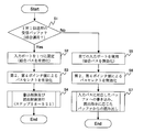
- FIG. 3 is a flowchart for explaining an initial setting procedure of normal operation and combined operation by the buffer device 2 of the present embodiment.
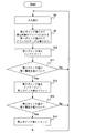
- FIG. 4 is a flowchart for explaining an operation example in the combined operation by the input control unit 4 of the buffer device 2 of the present embodiment.
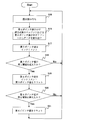
- FIG. 5 is an operation in the combined operation by the output control unit 6 of the buffer device 2 of the present embodiment. It is a flowchart explaining an example.
- FIG. 6 is a diagram for explaining an operation example in the combined operation of the buffer device 2 shown in FIG. First, an initial setting procedure in the buffer device 2 as an example of the present embodiment will be described with reference to FIG. First, it is determined by the firmware whether or not the buffer device 2 is used as a reception buffer for data transmission with one input and one output, that is, whether or not to perform a combined operation (step S1). This determination is made according to the connection topology for each buffer device 2 that functions as an output buffer mechanism provided in XB or the like in the system.
- step S1 by the firmware may be performed while the system is stopped, or may be performed by temporarily blocking data input to the buffer device 2 during system operation. If it is determined in step S1 that the buffer device 2 is used as a reception buffer for data transmission with one input and one output (Yes route in step S1), the buffer device is used as an initial setting for combined operation by the firmware. An input port 3 to which data is input when 2 performs one input and one output is specified. Then, information indicating the specified input port 3 is set in the setting register 47 by the firmware, and the specified input port 3 is fixedly used in the combined operation (step S2). That is, the coupling path 3D for outputting the data input from the specific input port 3 to the input switching unit 40 is validated by the firmware.
- the valid / invalid flag of the input control unit 4 and the output control unit 6 is set to be valid by the firmware (step S3). That is, the path selection by the second and fourth pointer values by the decoders 43d and 63b, that is, the selection of the selectors 43a to 43c based on the second pointer value and the selection of the reading paths 6A to 6C based on the fourth pointer value are performed. Enabled.
- the lower bit pointers 41 and 61 are diverted from the write control pointer 5a and the read control pointer 5b, the lower bit pointers for the diverted write control pointer 5a and read control pointer 5b are used by the firmware. Settings for use as 41 and 61 are validated. Further, the write control pointer 5a and the read control pointer 5b that are not diverted are invalidated by the firmware.
- Step S4 the buffer device 2 performs a coupling operation, and performs control of writing data input from a specific input port 3 to the coupling buffer 50 and control of reading data from the coupling buffer 50.
- Step S4 An example of the write control operation in step S4 will be described later with reference to steps S8 to S14 in FIG. 4 and FIG. 6, and an example of the read control operation will be described with reference to steps S15 to S21 in FIG. Reference will be made later.
- step S1 determines whether the buffer device 2 is not used as a reception buffer for data transmission with one input and one output (No route in step S1).
- the firmware performs initial setting for normal operation.
- the value set in the setting register 47 is reset (step S5). That is, the coupling path 3D is invalidated by the firmware, and all the input ports 3 are set to be usable.
- the valid / invalid flag of the input control unit 4 and the output control unit 6 is set to invalid by the firmware (step S6). That is, the path selection by the second and fourth pointer values by the decoders 43d and 63b, that is, the selection of the selectors 43a to 43c based on the second pointer value and the selection of the reading paths 6A to 6C based on the fourth pointer value are performed. It is invalidated.
- step S6 When the processing in step S6 is performed, in the buffer device 2, as a normal operation, data input from the input port 3 via the input paths 3A to 3C is controlled by the decoder 43d with respect to the selectors 43a to 43c. 5 is written. In the buffer device 2, as a normal operation, data is read from the read target buffer 5 according to the read instruction by controlling the read paths 6A to 6C by the arbitrating unit 66 and the decoder 63b (step S7).
- the input control unit 4 is in a state of waiting for input of data from the input port 3 (step S8).
- the input control unit 4 indicates the first pointer value of the lower bit pointer 41 in the write target buffer 5 indicated by the second pointer value of the upper bit pointer 42.
- Data is written at the address position (step S9).
- data input from the input port 3-1 is input to the selector 48a of the selection unit 48, and is input to the first switching unit 43 via the coupling path 3D.
- all the bits of the first pointer value and the second pointer value are “0”. Accordingly, the write target buffer 5 becomes the buffer 5-1 corresponding to the second pointer value “00”, and the input data from the coupling path 3D is transferred to the buffer 5-1 by the selector 43a selected by the decoder 43d. It is written (see (1) in FIG. 6).
- the first pointer value is incremented when data is written to any one of the buffers 5-1 to 5-3 constituting the combined buffer 50 (step S10). Each time data is written to the buffer 5, it is determined by the lower bit pointer 42 whether or not the first pointer value exceeds the first threshold value (step S11). If it is determined that the first pointer value does not exceed the first threshold value (No route in step S11), the process waits for input of the next data, and proceeds to step S8.
- step S11 if it is determined that the first pointer value has exceeded the first threshold value (Yes route in step S11), the buffer 5-1 is full, and the lower bit pointer 41 sets all the bits of the first pointer value. Reset to “0”. Further, the second pointer value of the upper bit pointer 42 is incremented (step S12). Further, every time the second pointer value is incremented, it is determined whether or not the second pointer value exceeds the second threshold value (step S13). If it is determined that the second pointer value does not exceed the second threshold value (No route in step S13), the process waits for input of the next data and proceeds to step S8.
- the write target buffer 5-1 is switched to the buffer 5-2 corresponding to the second pointer value “01”. Accordingly, the input data from the coupling path 3D is written into the buffer 5-2 by the selector 43b selected by the decoder 43d (see (2) in FIG. 6).
- the selector 43b selected by the decoder 43d
- the write target buffer 5-2 is switched to the buffer 5-3 corresponding to the second pointer value “10”. Accordingly, the input data from the coupling path 3D is written into the buffer 5-3 by the selector 43c selected by the decoder 43d (see (3) in FIG. 6).
- the first pointer value exceeds the first threshold value and the buffer 5-3 becomes full, all the bits of the first pointer value are reset to “0” and the second pointer value is incremented to “ 11 ”.
- the second pointer value is reset to “00” by the upper bit pointer 42 (step S14), and the write target buffer 5- 3 switches to the buffer 5-1. Accordingly, the input data from the coupling path 3D is written into the buffer 5-1 by the selector 43a selected by the decoder 43d (see (1) in FIG. 6).
- the input control unit 4 does not use the input paths 3A to 3C, but guides data from the specific input port 3 set in the setting register 47 to the combined path 3D. Also, the data input to the first switching unit 43 via the coupling path 3D is switched by the first switching unit 43 in accordance with changes in the first and second pointer values, and the buffer 5 to be written is switched. It is written to the combined buffer 50.
- the output switching unit 60 is in a state of waiting for a reading instruction from the arbitrating unit 66 (step S15).
- the output control unit 6 causes the address position indicated by the third pointer value of the lower bit pointer 61 in the buffer 5 to be read indicated by the fourth pointer value of the upper bit pointer 62. From this, data is read out (step S16).
- the third pointer value is incremented by the lower bit pointer 61 when a read instruction is input from the arbitration unit 66 (step S17). Each time the third pointer value is incremented, the lower bit pointer 62 determines whether or not the third pointer value exceeds the first threshold value (step S18). If it is determined that the third pointer value does not exceed the first threshold value (No route in step S18), the next read instruction is waited for, and the process proceeds to step S15.
- step S18 if it is determined that the third pointer value has exceeded the first threshold value (Yes route in step S18), the data is read to the end of the data storage area of the buffer 5-1, and the lower bit pointer 61 As a result, all the bits of the third pointer value are reset to “0”. Further, the fourth pointer value of the upper bit pointer 62 is incremented (step S19).
- step S20 it is determined whether or not the fourth pointer value exceeds the second threshold value. If it is determined that the fourth pointer value does not exceed the second threshold value (No route in step S20), the next read instruction is waited for, and the process proceeds to step S15. As the fourth pointer value is incremented, the buffer 5-1 to be read is switched to the buffer 5-2 corresponding to the fourth pointer value “01”. Accordingly, the data written in the buffer 5-2 is read through the read path 6B by the selector 63a to which the control signal from the decoder 63b is input (see (5) in FIG. 6).
- the third pointer value exceeds the first threshold value and data is read to the end of the data storage area of the buffer 5-2, all the bits of the third pointer value are reset to “0”.
- the fourth pointer value is incremented.
- the buffer 5-3 to be read is switched to the buffer 5-3 corresponding to the second pointer value “10”. Accordingly, the data written in the buffer 5-3 is read through the read path 6C by the selector 63a to which the control signal from the decoder 63b is inputted (see (6) in FIG. 6).
- the third pointer value exceeds the first threshold value and data is read to the end of the data storage area of the buffer 5-3, all the bits of the third pointer value are reset to “0”.
- the fourth pointer value is incremented to “11”.
- the fourth pointer value is reset to “00” by the upper bit pointer 62 (step S21), and the read target buffer 5-3 Is switched to the buffer 5-1. Accordingly, the data written in the buffer 5-1 is read through the read path 6A by the selector 63a to which the control signal from the decoder 63b is input (see (4) in FIG. 6).
- the data written to the combined buffer 50 is switched by the output control unit 6 in accordance with changes in the third and fourth pointer values, and the buffer 5 to be read is switched, and the corresponding read paths 6A to 6C are switched. And output to the output port 7.
- the input control unit 4 and the output control unit 6, which are buffer control devices, are provided to the input control unit 4 and the output control unit 6.
- the combination buffer 50 can be assigned to the specific input port 3 simply by performing the setting for performing the combination operation. That is, according to the buffer device 2, the buffer structure for selecting the input data from the plurality of input ports 3 and outputting it to the output path 7 can be easily switched to one FIFO structure.
- the buffer device 2 by providing a switching mechanism with the input control unit 4 and the output control unit 6 for the buffer devices of the plurality of input ports 3 and at least one output port 7, one-to-one transmission over a longer distance than before is possible. become. Therefore, according to the buffer device 2 as an example of the present embodiment, by providing a simple input / output port switching mechanism, the buffer device 2 can be used for long distance transmission, for example, with a simple configuration and simple control. The buffer capacity can be easily secured, and data transmission with one input and one output over a longer distance than before can be performed.
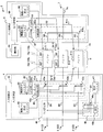
- FIG. 7 is a diagram illustrating a configuration example of the information processing system 1 according to the present embodiment.
- the direction of the arrow in FIG. 7 indicates the data transmission direction.
- FIG. 7 for simplification of the drawing, the internal configuration of the XB 12-1 and the partial configuration of the buffer devices 2-1 to 2-4 of the XB 12-2 are omitted.
- the XB 120 shown in FIG. 17 is configured as a dedicated chip in which the input ports 300-1 to 300-3 and the buffers 500-1 to 500-3 in the buffer devices 200-1 to 200-4 are associated in advance. Often.
- the XBs 120-1 and 120-2 shown in FIG. 18 described above have the same configuration as the XB 120 shown in FIG. 17, but the SBs 110-4 to 110-6 shown in FIG. 18 are buffer devices 200-2 to 200-4. Are connected so that they can communicate with each other. That is, the communication between the SBs 110-1 to 110-3 and the communication between the SBs 110-4 to 110-6 do not go through the XBs 120-1 and 120-2, respectively, but the SBs 110-1 to 110-3 that are separated from each other. And communication between the SBs 110-4 to 110-6 are performed via the XBs 120-1 and 120-2.
- the buffers D, E, G, I, K, and L in the buffer devices 200-2 to 200-4 shown in FIG. 18 become unused buffers in the XBs 120-1 and 120-2.
- sharing of parts has been promoted in the field of information processing systems for reasons such as cost reduction.
- either of the information processing systems 100-1 and 100-2 shown in FIGS. Even in the configuration, there is a desire to use the same XB chip.
- an LSI Large Scale Integration
- the information processing system 1 as an example of this embodiment illustrated in FIG. 7 includes SBs 11-1 to 11-6, XB 12-1, and XB 12-1 having the same connection relationship as the information processing system 100-2 illustrated in FIG. 12-2.
- the XB 12-2 includes buffer devices 2-1 to 2-4 respectively corresponding to the buffer device 2 according to the present embodiment.
- the XB 12-1 has the same configuration as the XB 12-2, although not shown in FIG. As shown in FIG. 7, the output side of the buffer device 2-1 in the XB 12-2, that is, the output port 7 (not shown) is connected to the XB 12-1 via a long-distance transmission path, and each of the buffer devices 2-2 to 2 is connected.
- the output side of -4 is connected to the corresponding SBs 11-4 to 11-6.
- the input side of the buffer device 2-1 in the XB 12-2, that is, the input ports 3-1 to 3-3 (not shown) are connected to the SBs 11-4 to 11-6, respectively, and the buffer devices 2-2 to 2-
- the input side of 4 is connected to the XB 12-1 via a long distance transmission path.
- the buffer device 2-2 receives the data input from the XB 12-1 through the long-distance transmission path and the specific input port 3, and the buffers D ⁇ F can be written.
- the buffer devices 2-3 and 2-4 receive the data input from the XB 12-1 via the long distance transmission path and the specific input port 3, and the buffers G to I and J configured as the coupling buffer 50 are used. ⁇ L can be written respectively.
- the buffer device 2 according to the present embodiment As described with reference to FIG. 7, by using the buffer device 2 according to the present embodiment, for example, the information processing systems 100-1 and 100-2 shown in FIGS. Can be controlled by the same XB chip. Therefore, according to the buffer device 2 according to the present embodiment, in the information processing system, it is possible to use an LSI more versatile than before with a simple configuration and simple control. That is, the buffer device 2 according to the present embodiment is particularly effective when applied to XB chips having various configurations.
- the first and third positions held by the lower bit pointers 41 and 61 are the data write position and the data read position in the buffer 5.
- the buffer 5 to be written and read is selected according to the second and fourth pointer values held by the upper bit pointers 42 and 62.
- the first switching unit 43 switches the writing target buffer 5 to another buffer 5 of the combined buffer 50 according to the information indicating the writing position, and the second switching unit 63 reads the reading target.
- the other buffer 5 is switched to the other buffer 5 in the combined buffer 50.
- the input setting unit 46 of the buffer device 2 information indicating the specific input port 3 allocated to the combined buffer 50 is held by the setting register 47, and a plurality of selection units 48 can store a plurality of information. Data input from a specific input port 3 among the input ports 3 is output to the input switching unit 40.
- the input port 3 assigned to the coupling buffer 50 can be determined by simple control that simply sets information indicating the specific input port 3 in the setting register 47. Further, the buffer 5 constituting the combined buffer 50 and the input port 3 allocated to the combined buffer 50 can be set and updated by firmware monitoring the buffer device 2.
- the setting of the coupling buffer 50 and the specific input port 3 by the firmware is changed, so that the system configuration can be changed flexibly. be able to. Even when the information processing system 1 to which the buffer device 2 is applied is in operation, the setting can be dynamically changed without bringing down the system.
- the buffer device 2 as an example of the present embodiment configured as described above can function as a reception buffer that performs one input and one output using a specific one input port 3 in combined operation. it can. However, depending on the configuration of the information processing system 1, that is, the connection topology, data transmission may be performed using a smaller number of input ports 3 than the normal operation among the input ports 3 of the buffer device 2.
- the firmware selects whether to perform normal operation using all the input ports 3 or combined operation using only one input port 3 in the buffer device 2 described above. Will do.
- the firmware selects the normal operation in the above-described buffer device 2 while some of the input ports 3 and the buffers 5 are not used. It will be.
- the buffer device 2 even when a number m of input ports 3 and buffers 5 smaller than the number n of input ports 3 in the buffer device 2 are used, the plurality of buffers 5 are logically arranged. Combined, it can function as a receive buffer that performs m inputs and 1 output.
- the operation of performing m input and 1 output is referred to as mixed operation.
- the buffer device 2 according to this modification will be described with reference to FIGS.
- FIG. 8 is a diagram illustrating a modification of the configuration of the buffer device 2 according to an embodiment.
- 9 and 10 are diagrams showing examples of path selection in the comparison circuits 43e and 63c of the buffer device 2 of the present modification.
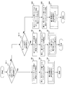
- FIG. 11 is a flowchart for explaining an initial setting procedure of normal operation, combined operation, and mixed operation by the buffer device 2 of the present modification.
- FIG. 12 is a flowchart for explaining an operation example in the mixed operation by the input control unit 4 of the buffer device 2 of the present modification.
- FIG. 13 shows an operation in the mixed operation by the output control unit 6 of the buffer device 2 of the present modification. It is a flowchart explaining an example.
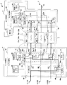
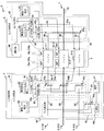
- 14 and 15 are diagrams for explaining an operation example in the mixed operation of the buffer device 2 shown in FIG.
- the buffer device 2 according to this modification shown in FIG. 8 First, a configuration example of the buffer device 2 according to this modification shown in FIG. 8 will be described.
- the input port 3-3 is not used, and the data input from the input port 3-1 by the input control unit 4 is selectively sent to the buffers 5-1 and 5-3.
- data input from the input port 3-2 is written to the buffer 5-2 in the same manner as in normal operation.
- the combined buffer 50 is configured by the buffers 5-1 and 5-3. Further, in the buffer device 2 according to this modification, the output controller 6 selectively reads out data from the buffers 5-1 and 5-3 and the buffer 5-2 that constitute the combined buffer 50, and outputs the data. Output from port 7.
- the input switching unit 40 of the input control unit 4 includes a multi-path setting register 45, and the first switching unit 43 includes a comparison circuit 43e instead of the decoder 43d.
- the output switching unit 60 of the output control unit 6 includes a multi-path setting register 65, and the second switching unit 63 includes a comparison circuit 63c instead of the decoder 63b.
- the arbitration unit 66 according to the present modification outputs a read instruction designating the read target buffer 5 to the output switching unit 60 in the mixed operation. That is, the arbitration unit 66 according to the present modification selects the output switching unit 60 at each timing of reading data from the buffer 5 in the same manner as the arbitration unit 66 in the normal operation of the buffer device 2 shown in FIG. The instruction to read the data written in the read target buffer 5 is output (issued).
- the buffer device 2 according to this modification is different from the buffer device 2 shown in FIG. 2 in the above-described points, but the other configurations are the same or substantially the same.
- the lower bit pointers 41 and 61 actually indicate lines 41a and 61a for designating the write and read positions of the buffer 5 constituting the combined buffer 50, respectively.
- the lower bit pointers 41 and 61 are connected to the buffer 5-2.
- the lines 41a and 61a connecting the lower bit pointers 41 and 61 and the buffer 5-2 are omitted for convenience of explanation.
- the line for the arbitration unit 66 to increment the read control pointer 5b of the buffer 5 in the normal operation actually includes the arbitration unit 66 and each of the read control pointers 5b-1 and 5b-3. Connecting.
- the arbitrating unit 66 and the read control pointers 5b-1 and 5b-3 are connected. Lines to be connected are omitted.
- the multiple path setting register 45 is a register that holds first buffer selection information corresponding to each of the buffers 5-1 to 5-3, that is, the selectors 43a to 43c.
- the first buffer selection information indicates a correspondence relationship between the second pointer value and the buffers 5-1 to 5-3 selected as the write target buffer 5, that is, the selectors 43a to 43c. It is set by the firmware in the initial setting or the like.
- the firmware can arbitrarily determine the order of the buffer 5 selected as the write target buffer 5 according to the register value set in the multiple path setting register 45.
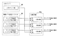
- the first buffer selection information includes “000” as the second pointer value corresponding to the buffer 5-1, that is, the selector 43a, and the buffer 5-2, that is, the selector 43b. “111” is set as the corresponding second pointer value, and “001” is set as the register value as the second pointer value corresponding to the buffer 5-3, that is, the selector 43c.
- the comparison circuit 43e selects the buffer 5 corresponding to the first buffer selection information that matches the second pointer value of the upper bit pointer 42 as the buffer 5 to be written. That is, the comparison circuit 43e switches the buffer 5 to be written in accordance with the change in the second pointer value, like the decoder 43d in the buffer device 2 shown in FIG.
- the register value “111” associated with the selector 43b is a special bit
- the second threshold is set to be equal to or less than the value of the special bit with respect to the threshold setting register 44 by the firmware in the initial setting of the mixed operation. Is set to be
- the buffer 5-2 not included in the combined buffer 50 is not designated by the second pointer value of the upper bit pointer 42 in the mixed operation. That is, the comparison circuit 43e does not output a control signal for selecting data input via the coupling bus 3D to the selector 43b corresponding to the buffer 5-2. In other words, in the mixed operation, the comparison circuit 43e replaces the buffer 5-2 corresponding to the selector 43b in which the special bit is set with the buffer 5 to be written related to the data input from the specific input port 3-1. Suppressing selection as
- the comparison circuit 43e sets the coupling path 3D to the selector 43a or 43c so as to select the buffer 5-1 or 5-3 as the write target buffer 5 in accordance with the change of the second pointer value.
- a control signal to be selected is output.
- the comparison circuit 43e outputs a control signal for selecting the corresponding input paths 3A to 3C to the selector 43b in which the special bit is set in the first buffer selection information.
- the first buffer selection information held by the multi-path setting register 45 includes the selectors 43a to 43c corresponding to the buffer 5 for performing input / output similar to the normal operation in the initial setting of the mixed operation. Special bits are set.
- the multiple path setting register 65 is a register that holds second buffer selection information corresponding to each of the buffers 5-1 to 5-3, that is, the read paths 6A to 6C.
- the second buffer selection information indicates the correspondence between the fourth pointer value and the buffers 5-1 to 5-3 selected as the buffer 5 to be read, that is, the read paths 6A to 6C. It is set by the firmware in the initial setting or the like. That is, the firmware can arbitrarily determine the order of the buffer 5 selected as the read target buffer 5 according to the register value set in the multiple path setting register 65.
- the comparison circuit 63c receives the fourth pointer value of the upper bit pointer 62 and the second buffer selection set in the read target buffer 5.
- a control signal is output to the selector 63a to read data from the buffer 5 to be read.
- the register value “111” associated with the read path 6B is a special bit
- the second threshold value is set in the threshold value setting register 64 to be equal to or less than the value of the special bit.
- the buffer 5-2 not included in the combined buffer 50 is not designated by the fourth pointer value of the upper bit pointer 62 in the mixed operation. That is, in the present modification, the second threshold value is “010”, and the fourth pointer value is “000” or “001” as shown in FIG.
- the comparison circuit 63c reads out the selector 63a so as to select the buffer 5-1 or 5-3 as the buffer 5 to be read in response to the read instruction from the arbitration unit 66 and the change in the fourth pointer value.
- a control signal for selecting the path 6A or 6C is output.
- the comparison circuit 63c sets the fourth pointer value. Regardless, the control signal for selecting the readout path 6B is output to the selector 63a. That is, the comparison circuit 63c compares the second buffer selection information with the fourth pointer value when the buffer 5 constituting the combined buffer 50 is designated as the read target buffer 5 in the read instruction from the arbitration unit 66. If they match, a control signal for reading data from the buffer 5 to be read is output to the selector 63a.
- the comparison circuit 63c compares the second buffer selection information with the fourth pointer value. Without performing this, a control signal for reading data from the buffer 5 to be read is output to the selector 63a.
- FIG. 11 is obtained by adding steps S1-2 and S22 to S24 to the operation example shown in FIG. Note that the Yes route in Step S1-1, the Yes route in Step S1-2, and the processing in Steps S2 to S5 are the same as the operation example shown in FIG.
- step S1-1 if the firmware determines that the buffer device 2 is not used as a reception buffer for one-to-one transmission (No route in step S1-1), all input ports 3 is used, that is, whether or not normal operation is performed is determined (step S1-2).
- all the input ports 3 are not used (No route of step S1-2)
- the buffer device 2 performs m input 1 output as the initial setting of the mixed operation by the firmware.
- the input port 3 to which data to be written to the coupling buffer 50 is input is specified.
- information indicating the specified input port 3 is set in the setting register 47 by the firmware, and the specified input port 3 is fixedly used for writing to the coupling buffer 50 (step S22). That is, the coupling path 3D for outputting the data input from the specific input port 3 to the input switching unit 40 is validated by the firmware.
- the valid / invalid flag of the input control unit 4 and the output control unit 6 is set to be valid by the firmware (step S23). That is, the path selection by the second and fourth pointer values by the comparison circuits 43e and 63c, that is, the selection of the selectors 43a to 43c based on the second pointer value and the selection of the read paths 6A to 6C based on the fourth pointer value Is activated.
- the firmware When the lower bit pointers 41 and 61 are diverted from the write control pointer 5a and the read control pointer 5b, the lower bit pointers for the diverted write control pointer 5a and read control pointer 5b are used by the firmware. Settings for use as 41 and 61 are validated. Further, the firmware invalidates the write control pointer 5a and the read control pointer 5b which are provided corresponding to the buffer 5 constituting the coupling buffer 50 and are not diverted.
- step S23 special bits having values not specified by the second and fourth pointer values are associated with the buffer 5 that does not constitute the combined buffer 50 in the multi-path setting registers 45 and 65. Further, the threshold value setting registers 45 and 65 are set with a second threshold value that is equal to or less than the value of the special bit.
- step S23 When the process of step S23 is performed, the mixed operation is performed in the buffer device 2, the write control to the combined buffer 50 of the data input from the specific input port 3, and the input ports 3 other than the specific input port 3 are performed. Is written to the corresponding buffer 5. Further, reading control of data from the coupling buffer 50 and the buffers 5 other than the coupling buffer 50 is performed (step S24).
- the buffer device 2 shown in FIGS. 14 and 15 has completed the processing of steps S22 and S23 of FIG.
- the case where the mixed operation of step S24 is performed as the input port 3 that performs input / output will be described.
- the first and second buffer selection information of the multi-path setting registers 45 and 65 shown in FIGS. 9 and 10 are set in the buffers 5-1 to 5-3, and the threshold setting registers 44 and 64 store the first information. A description will be given assuming that the threshold value “001” is set.
- the input control unit 4 is in a state of waiting for input of data from the input port 3 (step S25).
- the input control unit 4 causes the lower bit in the write target buffer 5 indicated by the second pointer value of the upper bit pointer 42.
- Data is written at the address position indicated by the first pointer value of the pointer 41 (step S27).
- the comparison circuit 43e outputs a control signal for selecting the coupling path 3D to the selector 43a corresponding to the second pointer value “000”. The Then, the data input from the input port 3-1 via the coupling path 3D is written to the address position indicated by the first pointer value in the corresponding buffer 5-1 via the selector 43a ((1 in FIG. 14). )reference).
- the comparison circuit 43e When the second pointer value is “001”, the comparison circuit 43e outputs a control signal for selecting the coupling path 3D to the selector 43c corresponding to the second pointer value “001”. Then, the data input from the input port 3-1 via the coupling path 3D is written to the address position indicated by the first pointer value in the corresponding buffer 5-3 via the selector 43c ((2 in FIG. 14). )reference).
- steps S28 to S32 is the same as the processing in steps S10 to S14 in FIG.
- the selector 43b receives a control signal for selecting the input path 3B by the comparison circuit 43e. Therefore, as shown in FIG. 15, the data input from the input port 3-2 via the input path 3B has the pointer value of the write control pointer 5a-2 of the buffer 5-2 via the selector 43b. It is written at the indicated address position (step S33).
- the data input to the first switching unit 43 from the input port 3-1 through the coupling path 3 ⁇ / b> D is transmitted to the first switching unit 43 by the first switching unit 43.
- the write target buffer 5 is switched and written into the combined buffer 50. Further, data input from the input port 3-2 to the first switching unit 43 via the input path 3B is written into the corresponding buffer 5 by the first switching unit 43.
- the output switching unit 60 is in a state of waiting for a reading instruction from the arbitrating unit 66 (step S34).
- the output control unit 6 determines whether the read instruction is from the buffer 5 in which the special bit is set. In other words, the output control unit 6 determines whether or not the buffer 5 to be read designated in the read instruction is a buffer 5 corresponding to the read paths 6A to 6C in which the special bit is set in the multiple path setting register 65. (Step S35).
- step S35 When it is not a read instruction from the buffer 5 in which the special bit is set (No route in step S35), the condition for reading data from the read target buffer 5 specified by the read instruction is satisfied by the comparison circuit 63c. Is determined (step S36). Specifically, in step S36, the comparison circuit 63c generates the register value of the second buffer selection information corresponding to the buffer 5 to be read designated by the read instruction and the fourth pointer value of the upper bit pointer 62. It is determined whether or not they match.
- step S36 If the condition is not satisfied (No route in step S36), the next read instruction is waited for, and the process proceeds to step S34. On the other hand, if the condition is satisfied (Yes route in step S36), the address position indicated by the third pointer value of the lower bit pointer 61 in the read target buffer 5 indicated by the fourth pointer value of the upper bit pointer 62 From this, data is read (step S37).
- the comparison circuit 63c outputs a control signal for causing the selector 63a to select the read path 6A corresponding to the fourth pointer value “000”. The Then, the data written in the buffer 5-1 is read out from the address position indicated by the third pointer value by the selector 63a through the read path 6A and output to the output port 7 ((3) in FIG. 14). reference).
- the comparison circuit 63c When the fourth pointer value is “001”, the comparison circuit 63c outputs a control signal that causes the selector 63a to select the read path 6C corresponding to the fourth pointer value “001”. Then, the data written in the buffer 5-3 is read out from the address position indicated by the third pointer value by the selector 63a through the read path 6C and is output to the output port 7 ((4) in FIG. 14). reference).
- steps S38 to S42 is the same as the processing in steps S17 to S21 in FIG.
- the output control unit 6 causes the read control pointer 5b in the read target buffer 5-2 to be read.
- the data is read from the address position indicated by -2 via the read path 3B and output to the output port 7 (step S33).
- step S33 the data written in the buffer 5-2 is read through the read path 6B by the selector 63a to which the control signal from the comparison circuit 63c is input.
- the data written in the combined buffer 50 is read out by the output control unit 6 in accordance with a read instruction and changes in the third and fourth pointer values. Are switched, read through the corresponding read path 6A or 6C, and output to the output port 7.
- the data written in the buffer 5-2 other than the coupling buffer 50 is selected by the output control unit 6 according to the reading instruction, read out through the corresponding reading path 6B, and output to the output port 7. Is done.
- the firmware sets special bits in the multiple path setting registers 45 and 65 for the buffer 5 that does not constitute the combined buffer 5, so that data input through a specific input port 3 is set.
- the buffer capacity is secured, and the corresponding buffer 5 can be used for another input port 3 that is not written to the combined buffer 50.
- the buffer device 2 shown in FIG. 2 includes a plurality of path setting registers 45 and 65, and has a simple configuration in which the comparison circuits 43e and 63c are provided instead of the decoders 43d and 63b, and m inputs and one output are provided.
- the reception buffer 2 to be performed can be realized.
- the buffer device 2 according to this modification shown in FIG. 8 can realize a mixed operation in which m inputs and 1 output are performed, and performs 1 input and 1 output as described above with reference to FIGS. 4 and 5. It is possible to realize a combined operation and a normal operation in which multiple inputs and outputs are performed as in the conventional case. Therefore, according to the buffer device 2 according to the present modification, a plurality of operation modes can be switched with a simple configuration and simple control, and a highly versatile reception buffer can be realized.
- the present invention is not limited to these specific embodiments and modifications, and does not depart from the spirit of the present invention.
- various modifications and changes can be made.
- the number of bits of the second and fourth pointer values in the buffer device 2 according to this embodiment is 2 bits
- the number of bits of the second and fourth pointer values in the buffer device 2 according to this modification is 3 bits.
- the present invention is not limited to this. That is, the number of bits of the second and fourth pointer values can be arbitrarily increased or decreased according to the number of input ports 3, that is, the number of buffers 5 that can form the combined buffer 50.
- the buffer device 2 according to the present embodiment and this modification, the case where the input port 3, the input paths 3A to 3C, and the three buffers 5 are provided has been described, but the present invention is not limited thereto, and the buffer device is not limited thereto. Any number may be provided according to the configuration of 2. Furthermore, in the buffer device 2 according to the present embodiment and this modification, the lower bit pointers 41 and 61 are obtained by diverting the write control pointer 5a-1 and the read control pointer 5b-1 provided in the buffer 5-1, respectively. Although there is, it is not limited to this. When the write control pointer 5a and the read control pointer 5b provided in the buffer 5 are diverted, the lower bit pointers 41 and 61 are written in any of the buffers 5 constituting the combined buffer 50. It may be a control pointer 5a and a read control pointer 5b.
Landscapes
- Engineering & Computer Science (AREA)
- Theoretical Computer Science (AREA)
- Physics & Mathematics (AREA)
- General Engineering & Computer Science (AREA)
- General Physics & Mathematics (AREA)
- Human Computer Interaction (AREA)
- Information Transfer Systems (AREA)
- Data Exchanges In Wide-Area Networks (AREA)
Abstract
複数の入力ポート(3)と、前記複数の入力ポート(3)それぞれから入力された情報が書き込まれる複数のバッファ(5)と、少なくとも1つの出力ポート(7)とを備えたバッファ装置であって、前記複数のバッファ(5)のうちの所定のバッファ群(50)に割り当てられた入力ポート(3)から情報が入力された場合、前記バッファ群(50)のバッファ(5)における書込位置を示す情報に基づいて前記バッファ群(50)から選択された書込対象のバッファ(5)に前記入力された情報を書き込むとともに、前記書込位置を示す情報に応じて、前記書込対象のバッファ(5)を前記バッファ群(50)のうちの他のバッファ(5)に切り替える入力切替部(40)と、前記バッファ群(50)のバッファ(5)における読出位置を示す情報に基づいて選択された読出対象のバッファ(5)から、情報を読み出して前記出力ポート(7)に出力する出力制御部(6)とを備える。
Description
本件は、情報処理システムにおけるバッファ装置,バッファ制御装置,及びバッファ制御方法に関する。
情報処理システムにおいて、複数のデータパスから入力されたデータを保持し、保持されたデータを1つのポートから出力する、例えば図16に示すような複数入力1出力に対応するバッファ装置が用いられることがある。
図16は、複数入力1出力に対応するバッファ装置200の構成例を示す図であり、図17及び図18は、図16に例示するバッファ装置200を備える情報処理システム100-1及び100-2の構成例をそれぞれ示す図である。
図16は、複数入力1出力に対応するバッファ装置200の構成例を示す図であり、図17及び図18は、図16に例示するバッファ装置200を備える情報処理システム100-1及び100-2の構成例をそれぞれ示す図である。
なお、図16では、3入力1出力に対応するバッファ装置200を示す。また、図17及び図18における矢印の向きは、データの伝送方向を示す。なお、図17及び図18では、図の簡略化のため、XB120-1の内部の構成、及びXB120-2のバッファ装置200-1~200-4の一部の構成を省略している。
図16に例示するように、バッファ装置200は、バッファ500-1~500-3を入力ポート300-1~300-3ごとに並列に備え、各バッファ500は、対応する入力ポート300-1~300-3から入力パス300A~300Cを介して入力されたデータを格納する。以下、バッファ500-1~500-3を区別しない場合には、単にバッファ500という。バッファ500としては、例えばRAM(Random Access Memory)等の揮発性メモリが挙げられる。
図16に例示するように、バッファ装置200は、バッファ500-1~500-3を入力ポート300-1~300-3ごとに並列に備え、各バッファ500は、対応する入力ポート300-1~300-3から入力パス300A~300Cを介して入力されたデータを格納する。以下、バッファ500-1~500-3を区別しない場合には、単にバッファ500という。バッファ500としては、例えばRAM(Random Access Memory)等の揮発性メモリが挙げられる。
また、バッファ装置200は、調停部660による調停結果に基づいて、出力するデータを出力対象のバッファ500から選択して出力パス700Aに出力する。つまり、出力対象のバッファ500から読み出したデータを出力ポート700から出力する。
バッファ装置200は、バッファ500それぞれに対応した書込制御ポインタ500a-1~500a-3及び読出制御ポインタ500b-1~500b-3を備える。以下、書込制御ポインタ500a-1~500a-3及び読出制御ポインタ500b-1~500b-3を区別しない場合には、それぞれ単に書込制御ポインタ500a及び読出制御ポインタ500bという。書込制御ポインタ500a及び読出制御ポインタ500bは、それぞれ図16中、WP及びRPと表記している。
バッファ装置200は、バッファ500それぞれに対応した書込制御ポインタ500a-1~500a-3及び読出制御ポインタ500b-1~500b-3を備える。以下、書込制御ポインタ500a-1~500a-3及び読出制御ポインタ500b-1~500b-3を区別しない場合には、それぞれ単に書込制御ポインタ500a及び読出制御ポインタ500bという。書込制御ポインタ500a及び読出制御ポインタ500bは、それぞれ図16中、WP及びRPと表記している。
書込制御ポインタ500aには、バッファ500の書き込みアドレスがポインタ値として記録されており、バッファ500への入力データは、対応する書込制御ポインタ500aのポインタ値が示すアドレス位置に書き込まれる。また、書込制御ポインタ500aは、対応するバッファ500に入力データが書き込まれるごとに、対応するポインタ値をインクリメントさせる。
読出制御ポインタ500bには、バッファ500からの出力データの読み出しアドレスがポインタ値として記録されており、バッファ500に格納されたデータは、対応する読出制御ポインタ500bのポインタ値が示すアドレス位置から読み出される。また、読出制御ポインタ500bは、対応するバッファ500から出力データが読み出されるごとに、自身のポインタ値をインクリメントさせる。
調停部660は、バッファ500からのデータの読出タイミングの調整、及び読出対象のバッファ500の選択(調停)を行なう。調停部660は、セレクタ630に対して、読出タイミングごとに、調停結果として読出対象のバッファ500を選択させる制御信号を出力する。なお、調停部660は、読出対象のバッファ500の選択を、例えばLRU(Least Recently Used)方式やラウンドロビン方式を用いて行なう。
セレクタ630は、調停部660による調停結果に基づき、読出対象のバッファ500に対応する読出制御ポインタ500bのポインタ値が示すアドレス位置から、出力データを読み出し、出力パス700Aに出力するものである。
なお、入力ポート300-1~300-3及び出力ポート700には、それぞれ、例えばサーバ等の情報処理装置やシステムボード(SB;System Board:以下、SBという)等が接続される。
なお、入力ポート300-1~300-3及び出力ポート700には、それぞれ、例えばサーバ等の情報処理装置やシステムボード(SB;System Board:以下、SBという)等が接続される。
図16に示すバッファ装置200は、例えば、図17に示す情報処理システム100-1や図18に示す情報処理システム100-2において、クロスバチップ(XB;Cross Bar:以下、XBという)等に備えられる。
図17に示す例において、バッファ装置200にそれぞれ対応するバッファ装置200-1~200-4は、XB120に備えられる。また、各バッファ装置200-1~200-4の出力側、つまり出力ポート700は、対応するSB110-1~110-4に接続され、各バッファ装置200-1~200-4の入力側、つまり入力ポート300-1~300-3は、対応するSB以外のSB110-1~110-4にそれぞれ接続される。
図17に示す例において、バッファ装置200にそれぞれ対応するバッファ装置200-1~200-4は、XB120に備えられる。また、各バッファ装置200-1~200-4の出力側、つまり出力ポート700は、対応するSB110-1~110-4に接続され、各バッファ装置200-1~200-4の入力側、つまり入力ポート300-1~300-3は、対応するSB以外のSB110-1~110-4にそれぞれ接続される。
図17に例示するバッファ装置200-1~200-4により、SB110-1~110-4は、それぞれXB120を介して、相互に通信可能に接続される。
図18に例示する情報処理システム100-2は、長距離伝送パスを介して相互に通信可能に接続されたXB120-1及び120-2を備える。XB120-1は、相互に通信可能に接続されたSB110-1~110-3を備え、XB120-2は、相互に通信可能に接続されたSB110-4~110-6を備える。
図18に例示する情報処理システム100-2は、長距離伝送パスを介して相互に通信可能に接続されたXB120-1及び120-2を備える。XB120-1は、相互に通信可能に接続されたSB110-1~110-3を備え、XB120-2は、相互に通信可能に接続されたSB110-4~110-6を備える。
図18に示す例において、XB120-2は、図17に示すXB120と同様に、バッファ装置200にそれぞれ対応するバッファ装置200-1~200-4を備える。なお、XB120-1は、図18において図示は省略しているが、XB120-2や図17に示すXB120と同様の構成である。
図18に例示するように、XB120-2におけるバッファ装置200-1の出力側は、長距離伝送パスを介してXB120-1に接続され、各バッファ装置200-2~200-4の出力側は、対応するSB110-4~110-6に接続される。一方、XB120-2におけるバッファ装置200-1の入力側は、SB110-4~110-6にそれぞれ接続される。また、XB120-2における各バッファ装置200-2~200-4の入力側は、対応するSB以外のSB110-4~110-6、及び長距離伝送パスを介してXB120-1にそれぞれ接続される。
図18に例示するように、XB120-2におけるバッファ装置200-1の出力側は、長距離伝送パスを介してXB120-1に接続され、各バッファ装置200-2~200-4の出力側は、対応するSB110-4~110-6に接続される。一方、XB120-2におけるバッファ装置200-1の入力側は、SB110-4~110-6にそれぞれ接続される。また、XB120-2における各バッファ装置200-2~200-4の入力側は、対応するSB以外のSB110-4~110-6、及び長距離伝送パスを介してXB120-1にそれぞれ接続される。
図18に例示する情報処理システム100-2においても、情報処理システム100-1と同様に、SB110-1~110-3とSB110-4~110-6とは、XB120-1、長距離伝送パス、及びXB120-2を介して、相互に通信可能に接続される。
なお、関連する技術として、空きFIFO(First In, First Out)の番号を記憶する空きFIFOキューを備え、書き込みポインタの示すFIFOに容量がなくなると、空きFIFOキューから空きFIFO番号を書き込みポインタへ読み出して、空きFIFOに書き込みを行なう技術がある。
なお、関連する技術として、空きFIFO(First In, First Out)の番号を記憶する空きFIFOキューを備え、書き込みポインタの示すFIFOに容量がなくなると、空きFIFOキューから空きFIFO番号を書き込みポインタへ読み出して、空きFIFOに書き込みを行なう技術がある。
パケット等のデータの伝送において、受信バッファの容量は、伝送距離に大きく影響される。
例えば、受信バッファが溢れることを防ぐための手法として、受信バッファや受信バッファに接続された受信側の装置が、送信側の装置に対してビジー(busy)信号を送信する等の手法が採られることがある。送信側の装置は、ビジー信号を受信するとデータの送信を抑止するが、伝送距離が長いほど、ビジー信号が送信されてから送信側の装置により受信されるまでに時間がかかるため、送信側の装置がデータ送信を抑止するまでに時間がかかる。
例えば、受信バッファが溢れることを防ぐための手法として、受信バッファや受信バッファに接続された受信側の装置が、送信側の装置に対してビジー(busy)信号を送信する等の手法が採られることがある。送信側の装置は、ビジー信号を受信するとデータの送信を抑止するが、伝送距離が長いほど、ビジー信号が送信されてから送信側の装置により受信されるまでに時間がかかるため、送信側の装置がデータ送信を抑止するまでに時間がかかる。
従って、データ伝送に用いられる受信バッファは、伝送距離が長いほどより多くのデータを溜め込むこと、つまり多くのデータが格納可能であることが要求される。すなわち、長距離伝送において用いられる受信バッファの容量を確保することは、長距離伝送における重要な問題の一つであるといえる。
なお、受信バッファの容量を確保する手法として、上述した空きFIFOの番号を記憶する空きFIFOキューを備える技術が挙げられる。
なお、受信バッファの容量を確保する手法として、上述した空きFIFOの番号を記憶する空きFIFOキューを備える技術が挙げられる。
しかしながら、空きFIFOキューを備える技術において、書き込み手段は、空きFIFOを使用する際に、これまで書き込みを行なっていたFIFO内に専用のフラグや空きFIFO番号を書き込むため、FIFOへの書き込みデータに対して細工が必要となる。また、書き込み手段や読み出し手段は、それぞれ書き込みや読み出しの際に、専用のフラグの有無とバッファ番号とに基づいて、書き込みポインタや読み出しポインタを書き換える処理を行なう必要がある。
このように、空きFIFOキューを備える技術において、書き込み又は読み出しFIFOの切り替えに係る制御は、簡便な制御とは言い難い。
ここまで、バッファ装置がXBに複数備えられ、複数の情報処理装置やSB等が、XBを介して相互に通信可能に接続される場合について説明したが、複数の情報処理装置やSB等が、1つのバッファ装置を介して、相互に通信可能に接続される場合においても同様の問題がある。
ここまで、バッファ装置がXBに複数備えられ、複数の情報処理装置やSB等が、XBを介して相互に通信可能に接続される場合について説明したが、複数の情報処理装置やSB等が、1つのバッファ装置を介して、相互に通信可能に接続される場合においても同様の問題がある。
上述の点に鑑み、本件の目的の1つは、簡素な構成により、バッファ装置におけるバッファ容量を容易に確保することである。
なお、前記目的に限らず、後述する発明を実施するための形態に示す各構成により導かれる作用効果であって、従来の技術によっては得られない作用効果を奏することも本発明の他の目的の1つとして位置付けることができる。
なお、前記目的に限らず、後述する発明を実施するための形態に示す各構成により導かれる作用効果であって、従来の技術によっては得られない作用効果を奏することも本発明の他の目的の1つとして位置付けることができる。
本件のバッファ装置は、複数の入力ポートと、前記複数の入力ポートそれぞれから入力された情報が書き込まれる複数のバッファと、前記バッファから読み出された情報が出力される少なくとも1つの出力ポートとを備えたバッファ装置であって、前記複数のバッファのうちの所定のバッファ群に割り当てられた入力ポートから情報が入力された場合、前記バッファ群のバッファにおける書込位置を示す情報に基づいて前記バッファ群から選択された書込対象のバッファに前記入力された情報を書き込むとともに、前記書込位置を示す情報に応じて、前記書込対象のバッファを前記バッファ群のうちの他のバッファに切り替える入力切替部と、前記バッファ群のバッファにおける読出位置を示す情報に基づいて選択された読出対象のバッファから、情報を読み出して前記出力ポートに出力する出力制御部とを備えるものである。
また、本件のバッファ制御装置は、上記バッファ装置における入力制御部及び出力制御部を備えるものである。
さらに、本件のバッファ制御方法は、複数の入力ポートと、前記複数の入力ポートそれぞれから入力された情報が書き込まれる複数のバッファと、前記バッファから読み出された情報が出力される少なくとも1つの出力ポートとを備えたバッファ装置におけるバッファ制御方法であって、前記複数のバッファのうちの所定のバッファ群に割り当てられた入力ポートから情報が入力された場合、前記バッファ群のバッファにおける書込位置を示す情報に基づいて、前記バッファ群から書込対象のバッファを選択し、前記選択された書込対象のバッファに前記入力された情報を書き込み、前記書込位置を示す情報に応じて、前記書込対象のバッファを前記バッファ群のうちの他のバッファに切り替え、前記バッファ群のバッファにおける読出位置を示す情報に基づいて、前記バッファ群から読出対象のバッファを選択し、前記選択された読出対象のバッファから、情報を読み出して前記出力ポートに出力するものである。
さらに、本件のバッファ制御方法は、複数の入力ポートと、前記複数の入力ポートそれぞれから入力された情報が書き込まれる複数のバッファと、前記バッファから読み出された情報が出力される少なくとも1つの出力ポートとを備えたバッファ装置におけるバッファ制御方法であって、前記複数のバッファのうちの所定のバッファ群に割り当てられた入力ポートから情報が入力された場合、前記バッファ群のバッファにおける書込位置を示す情報に基づいて、前記バッファ群から書込対象のバッファを選択し、前記選択された書込対象のバッファに前記入力された情報を書き込み、前記書込位置を示す情報に応じて、前記書込対象のバッファを前記バッファ群のうちの他のバッファに切り替え、前記バッファ群のバッファにおける読出位置を示す情報に基づいて、前記バッファ群から読出対象のバッファを選択し、前記選択された読出対象のバッファから、情報を読み出して前記出力ポートに出力するものである。
開示の技術によれば、簡素な構成により、バッファ装置におけるバッファ容量を容易に確保することができる。
以下、図面を参照して本発明の実施の形態を説明する。
〔1〕一実施形態
〔1-1〕一実施形態の構成
図1は、一実施形態に係るバッファ装置2の構成例を示す図である。
図1に示すように、バッファ装置2は、複数、例えば3つの入力ポート3-1~3-3、入力制御部4、複数、例えば3つのバッファ5-1~5-3、出力制御部6、及び出力ポート7を備える。なお、以下、特に区別しない場合には、入力ポート3-1~3-3を単に入力ポート3といい、バッファ5-1~5-3を単にバッファ5という。
〔1〕一実施形態
〔1-1〕一実施形態の構成
図1は、一実施形態に係るバッファ装置2の構成例を示す図である。
図1に示すように、バッファ装置2は、複数、例えば3つの入力ポート3-1~3-3、入力制御部4、複数、例えば3つのバッファ5-1~5-3、出力制御部6、及び出力ポート7を備える。なお、以下、特に区別しない場合には、入力ポート3-1~3-3を単に入力ポート3といい、バッファ5-1~5-3を単にバッファ5という。
バッファ装置2は、例えばサーバ等の情報処理装置やSB等の、図示しない外部の装置間で伝送されるパケット等のデータ、つまり情報を中継する装置である。以下、外部の装置を単に外部装置という。
入力ポート3は、それぞれ、送信側の外部装置からバッファ装置2に入力されるデータを受け入れるポートであり、伝送パスを介して送信側の外部装置に接続される。入力ポート3-1~3-3に入力されたデータは、それぞれ入力パス3A~3Cを介して入力制御部4に入力される。
入力ポート3は、それぞれ、送信側の外部装置からバッファ装置2に入力されるデータを受け入れるポートであり、伝送パスを介して送信側の外部装置に接続される。入力ポート3-1~3-3に入力されたデータは、それぞれ入力パス3A~3Cを介して入力制御部4に入力される。
入力パス3A~3Cは、それぞれ、一端が入力ポート3-1~3-3に接続され、他端が入力制御部4に接続されたパスである。
バッファ5は、入力ポート3-1~3-3ごとに並列に備えられ、入力ポート3それぞれから入力されたデータが、入力制御部4を介して書き込まれる記憶装置である。バッファ5に書き込まれたデータは、出力制御部6により読み出され、出力パス7Aを介して出力ポート7から出力される。なお、バッファ5としては、例えばRAM等の揮発性メモリが挙げられる。
バッファ5は、入力ポート3-1~3-3ごとに並列に備えられ、入力ポート3それぞれから入力されたデータが、入力制御部4を介して書き込まれる記憶装置である。バッファ5に書き込まれたデータは、出力制御部6により読み出され、出力パス7Aを介して出力ポート7から出力される。なお、バッファ5としては、例えばRAM等の揮発性メモリが挙げられる。
出力ポート7は、出力制御部6によってバッファ5から読み出されたデータをバッファ装置2から受信側の外部装置に出力する少なくとも1つのポートであり、伝送パスを介して受信側の外部装置に接続される。
出力パス7Aは、一端が出力制御部6に接続され、他端が出力ポート7に接続されたパスである。
出力パス7Aは、一端が出力制御部6に接続され、他端が出力ポート7に接続されたパスである。
ここで、本実施形態に係るバッファ装置2は、入力制御部4及び出力制御部6により、複数入力1出力を行なう運用と、複数のバッファ5を論理的に結合して、1入力1出力を行なう運用と、を切り替えて運用することができる。以下、バッファ装置2が複数入力1出力を行なう運用を通常運用といい、1入力1出力を行なう運用を結合運用という。
具体的に、結合運用は、データ伝送に係るバッファ容量を確保するために行なわれるバッファ装置2の運用の形態の一つであり、入力制御部4により、通常運用における入力ポート3とバッファ5との対応関係が、所定の対応関係に切り替えられる運用をいう。
具体的に、結合運用は、データ伝送に係るバッファ容量を確保するために行なわれるバッファ装置2の運用の形態の一つであり、入力制御部4により、通常運用における入力ポート3とバッファ5との対応関係が、所定の対応関係に切り替えられる運用をいう。
例えば、複数の入力ポート3-1~3-3全てからではなく、入力ポート3-1~3-3のいずれか1つのポート3から入力されたデータを1つの出力ポート7に出力したい場合、使用しない入力ポート3-1~3-3に対応して備えられたバッファ資源は未使用領域となる。
本実施形態では、この未使用領域のバッファ5を活用して、結合運用において、バッファ装置2における、例えば長距離伝送を行なうことが可能なバッファ容量を確保する。
本実施形態では、この未使用領域のバッファ5を活用して、結合運用において、バッファ装置2における、例えば長距離伝送を行なうことが可能なバッファ容量を確保する。
入力制御部4は、バッファ装置2の結合運用において、特定の入力ポート3から入力されたデータを、バッファ5のうちの一部又は全部のバッファ5を論理的に結合した、所定の結合バッファ(バッファ群)50に対して書き込む。
図1に例示する結合バッファ50は、バッファ5-1~5-3のうちの全部のバッファ5により構成される。また、図1に例示する結合バッファ50は、特定の入力ポートとして入力ポート3-1が割り当てられる。つまり、バッファ5の結合運用において、特定の入力ポートである入力ポート3-1から入力されたデータは、入力制御部4によって、結合バッファ50を構成するバッファ5-1~5-3に対して書き込まれる。
図1に例示する結合バッファ50は、バッファ5-1~5-3のうちの全部のバッファ5により構成される。また、図1に例示する結合バッファ50は、特定の入力ポートとして入力ポート3-1が割り当てられる。つまり、バッファ5の結合運用において、特定の入力ポートである入力ポート3-1から入力されたデータは、入力制御部4によって、結合バッファ50を構成するバッファ5-1~5-3に対して書き込まれる。
具体的には、入力制御部4(後述する入力切替部40)は、結合運用において、結合バッファ50に割り当てられた入力ポート3-1からデータが入力された場合、結合バッファ50を構成するバッファ5-1~5-3における、書込位置を示す情報に基づいて、結合バッファ50から書込対象のバッファ5を選択する。そして、入力制御部4は、選択した書込対象のバッファ5に、入力ポート3-1から入力されたデータを書き込む。なお、入力制御部4による、書込位置を示す情報に基づいた書込対象のバッファ5の選択の手法については、入力制御部4の詳細な構成の説明とともに、図2を用いて後述する。
また、入力制御部4は、バッファ装置2の通常運用において、入力ポート3-1~3-3から入力パス3A~3Cを介して入力されたデータを、対応するバッファ5に対して書き込む。具体的には、入力制御部4は、通常運用において、入力ポート3-1から入力パス3Aを介して入力されたデータをバッファ5-1に書き込む。同様に、入力制御部4は、通常運用において、入力ポート3-2から入力パス3Bを介して入力されたデータをバッファ5-2に書き込み、入力ポート3-3から入力パス3Cを介して入力されたデータをバッファ5-3に書き込む。
出力制御部6は、結合運用において、結合バッファ50を構成するバッファ5-1~5-3における、読出位置を示す情報に基づいて、結合バッファ50から読出対象のバッファ5を選択する。そして、出力制御部6は、選択した読出対象のバッファ5からデータを読み出して出力ポート7に出力する。なお、出力制御部6による、読出位置を示す情報に基づいた読出対象のバッファ5の選択の手法については、出力制御部6の詳細な構成の説明とともに、図2を用いて後述する。
また、出力制御部6は、通常運用において、バッファ5-1~5-3から読出対象のバッファ5を選択し、選択した読出対象のバッファ5に書き込まれたデータを読み出して、出力ポート7に対して出力する。
上述のように、図1に例示するバッファ装置2は、結合運用において、入力ポート3-1に入力されたデータを出力ポート7から出力する、1入力1出力に対応した受信バッファとして機能する。
上述のように、図1に例示するバッファ装置2は、結合運用において、入力ポート3-1に入力されたデータを出力ポート7から出力する、1入力1出力に対応した受信バッファとして機能する。
また、入力制御部4及び出力制御部6は、バッファ装置2の運用の形態に応じて、バッファ5に対するデータの書き込み及び読み出しの制御を行なう、バッファ制御装置として機能する。
〔1-2〕バッファ装置の詳細な構成
次に、上述したバッファ装置2の詳細な構成を、図2を用いて説明する。
〔1-2〕バッファ装置の詳細な構成
次に、上述したバッファ装置2の詳細な構成を、図2を用いて説明する。
図2は、図1に示すバッファ装置2の詳細な構成例を示す図である。
なお、図2に例示するバッファ装置2における結合バッファ50は、バッファ5-1~5-3により構成されるものとして説明する。
バッファ装置2は、バッファ5-1~5-3それぞれに対応した書込制御ポインタ5a-1~5a-3及び読出制御ポインタ5b-1~5b-3を備える。なお、図の簡略化のために、図2において、バッファ5-1に対応した書込制御ポインタ5a-1及び読出制御ポインタ5b-1のみを図示している。以下、書込制御ポインタ5a-1~5a-3及び読出制御ポインタ5b-1~5b-3を区別しない場合には、それぞれ単に書込制御ポインタ5a及び読出制御ポインタ5bという。図2において、書込制御ポインタ5a及び読出制御ポインタ5bは、それぞれWP及びRPと表記している。
なお、図2に例示するバッファ装置2における結合バッファ50は、バッファ5-1~5-3により構成されるものとして説明する。
バッファ装置2は、バッファ5-1~5-3それぞれに対応した書込制御ポインタ5a-1~5a-3及び読出制御ポインタ5b-1~5b-3を備える。なお、図の簡略化のために、図2において、バッファ5-1に対応した書込制御ポインタ5a-1及び読出制御ポインタ5b-1のみを図示している。以下、書込制御ポインタ5a-1~5a-3及び読出制御ポインタ5b-1~5b-3を区別しない場合には、それぞれ単に書込制御ポインタ5a及び読出制御ポインタ5bという。図2において、書込制御ポインタ5a及び読出制御ポインタ5bは、それぞれWP及びRPと表記している。
通常運用において、書込制御ポインタ5aには、対応するバッファ5への書込位置を示す書き込みアドレスがポインタ値として記録されており、バッファ5への入力データは、入力制御部4によって、対応する書込制御ポインタ5aのポインタ値が示すアドレス位置に書き込まれる。また、通常運用において、書込制御ポインタ5aは、対応するバッファ5に入力データが書き込まれるごとに、自身のポインタ値を変化、例えばインクリメントさせる。
通常運用において、読出制御ポインタ5bには、対応するバッファ5からの出力データの読出位置を示す読み出しアドレスがポインタ値として記録されており、バッファ5からの出力データは、出力制御部6によって、対応する読出制御ポインタ5bのポインタ値が示すアドレス位置から読み出される。また、通常運用において、読出制御ポインタ5bは、対応するバッファ5から出力データが読み出されるごとに、自身のポインタ値を変化、例えばインクリメントさせる。
なお、書込制御ポインタ5a及び読出制御ポインタ5bのポインタ値は、それぞれ、例えばインクリメントによって、バッファ5における使用可能なアドレスの上限等を超えた場合、書込制御ポインタ5a及び読出制御ポインタ5bにより初期値にリセットされる。
〔1-2-1〕入力制御部の詳細な構成
入力制御部4は、入力切替部40、及び入力設定部46を備える。
〔1-2-1〕入力制御部の詳細な構成
入力制御部4は、入力切替部40、及び入力設定部46を備える。
入力設定部46は、通常運用及び結合運用のいずれの運用においても、入力ポート3-1~3-3から入力されたデータを、対応する入力パス3A~3Cを介して、入力切替部40に出力する。
また、入力設定部46は、結合運用において、結合バッファ50に割り当てられた特定の入力ポート3からデータが入力された場合に、入力されたデータを結合パス3Dを介して、入力切替部40に出力する。
また、入力設定部46は、結合運用において、結合バッファ50に割り当てられた特定の入力ポート3からデータが入力された場合に、入力されたデータを結合パス3Dを介して、入力切替部40に出力する。
入力切替部40は、通常運用において、入力設定部46から入力パス3A~3Cを介して入力されたデータを、対応するバッファ5-1~5-3に書き込む。
また、入力切替部40は、結合運用において、入力設定部46から結合パス3Dを介して入力されたデータを、結合バッファ50の書込対象のバッファ5に書き込む。
すなわち、入力制御部4は、入力切替部40及び入力設定部46によって、通常運用においては、入力ポート3-1~3-3から入力パス3A~3Cを介して入力されたデータを対応するバッファ5に書き込む。一方、入力制御部4は、結合運用においては、特定の入力ポート3から結合パス3Dを介して入力されたデータを、結合バッファ50における書込対象のバッファ5に書き込む。
また、入力切替部40は、結合運用において、入力設定部46から結合パス3Dを介して入力されたデータを、結合バッファ50の書込対象のバッファ5に書き込む。
すなわち、入力制御部4は、入力切替部40及び入力設定部46によって、通常運用においては、入力ポート3-1~3-3から入力パス3A~3Cを介して入力されたデータを対応するバッファ5に書き込む。一方、入力制御部4は、結合運用においては、特定の入力ポート3から結合パス3Dを介して入力されたデータを、結合バッファ50における書込対象のバッファ5に書き込む。
以下、入力切替部40及び入力設定部46の詳細な構成について説明する。
はじめに、入力設定部46について説明する。
入力設定部46は、設定レジスタ(第2レジスタ)47、及び選択部48を備える。
設定レジスタ47は、結合バッファ50に割り当てられた特定の入力ポート3、つまり特定の入力パス3A~3Cを示す情報を、例えば結合運用の初期設定において設定され、保持するものである。以下、設定レジスタ47は、特定の入力ポート3として入力ポート3-1を示す情報を保持するものとして説明する。
はじめに、入力設定部46について説明する。
入力設定部46は、設定レジスタ(第2レジスタ)47、及び選択部48を備える。
設定レジスタ47は、結合バッファ50に割り当てられた特定の入力ポート3、つまり特定の入力パス3A~3Cを示す情報を、例えば結合運用の初期設定において設定され、保持するものである。以下、設定レジスタ47は、特定の入力ポート3として入力ポート3-1を示す情報を保持するものとして説明する。
選択部48は、結合運用において、設定レジスタ47に保持された情報に基づいて、複数の入力ポート3-1~3-3から結合バッファ50に割り当てられた入力ポート3を選択し、選択した入力ポート3から入力されたデータを、結合パス3Dを介して入力切替部40に出力する。
選択部48は、セレクタ48a、及びデコーダ48bを備える。
選択部48は、セレクタ48a、及びデコーダ48bを備える。
セレクタ48aは、入力パス3A~3Cそれぞれから分岐した複数のパスが入力側に接続される一方、結合パス3Dが出力側に接続される。
デコーダ48bは、設定レジスタ47に保持された情報に基づいて、結合バッファ50に割り当てられた特定の入力ポート3に対応するパスを選択するように、セレクタ48aに対して制御信号(選択信号)を出力する。なお、デコーダ48bは、図2中、DECと表記している。
デコーダ48bは、設定レジスタ47に保持された情報に基づいて、結合バッファ50に割り当てられた特定の入力ポート3に対応するパスを選択するように、セレクタ48aに対して制御信号(選択信号)を出力する。なお、デコーダ48bは、図2中、DECと表記している。
つまり、セレクタ48aは、結合運用において、デコーダ48bからの制御信号によって選択されたパス、すなわち入力ポート3-1に対応するパスを、入力側に接続された複数のパスから選択する。そして、セレクタ48aは、選択したパスを介して入力ポート3-1から入力されるデータを、結合パス3Dに出力する。
なお、既述の如く、設定レジスタ47に設定されるレジスタ値等の情報により、結合バッファ50に割り当てられる特定の入力ポート3が決定される。この設定レジスタ47への設定は、本実施形態のバッファ装置2が適用されるXBと、周辺のSBや他のXB等のLSIとの接続トポロジにより決定されるものである。
なお、既述の如く、設定レジスタ47に設定されるレジスタ値等の情報により、結合バッファ50に割り当てられる特定の入力ポート3が決定される。この設定レジスタ47への設定は、本実施形態のバッファ装置2が適用されるXBと、周辺のSBや他のXB等のLSIとの接続トポロジにより決定されるものである。
システム構成の変更等によって接続トポロジが変更される際には、例えばバッファ装置2が適用されたシステム構成を監視するファームウェアや、システムの管理者等が、設定レジスタ47に対して適切なレジスタ値等の情報を設定し直すことができる。以下、ファームウェアや、システムの管理者等をまとめてファームウェアという。
つまり、ファームウェアは、システム構成の変更により、バッファ装置2が例えば1入力1出力の受信バッファとして用いられる場合には、設定レジスタ47に対して特定の入力ポート3を設定することができる。また、ファームウェアは、システム構成の変更により、バッファ装置2が複数入力1出力の受信バッファとして用いられる場合には、設定レジスタ47に設定された特定の入力ポート3をリセットして、バッファ装置2を通常運用を行なうべく構成することができる。
つまり、ファームウェアは、システム構成の変更により、バッファ装置2が例えば1入力1出力の受信バッファとして用いられる場合には、設定レジスタ47に対して特定の入力ポート3を設定することができる。また、ファームウェアは、システム構成の変更により、バッファ装置2が複数入力1出力の受信バッファとして用いられる場合には、設定レジスタ47に設定された特定の入力ポート3をリセットして、バッファ装置2を通常運用を行なうべく構成することができる。
ファームウェアによる設定レジスタ47の設定値の変更は、バッファ装置2が適用されたシステムが運用中であっても同様に行なうことができる。例えば、バッファ装置2やバッファ装置2が適用されたXB等に、設定レジスタ47の設定変更を行なうバッファ装置2へ到来するデータを一時的に遮断する機能を設けることで、システムをダウンさせることなく、動的に設定レジスタ47の設定変更ができる。
次に、入力切替部40について説明する。
入力切替部40は、結合運用において、結合バッファ50のバッファ5における書込位置を示す情報に応じて、書込対象のバッファ5を結合バッファ50のうちの他のバッファ5に切り替える。
入力切替部40は、下位ビットポインタ(第1ポインタ)41、上位ビットポインタ(第2ポインタ)42、第1切替部43、及び閾値設定レジスタ44を備える。
入力切替部40は、結合運用において、結合バッファ50のバッファ5における書込位置を示す情報に応じて、書込対象のバッファ5を結合バッファ50のうちの他のバッファ5に切り替える。
入力切替部40は、下位ビットポインタ(第1ポインタ)41、上位ビットポインタ(第2ポインタ)42、第1切替部43、及び閾値設定レジスタ44を備える。
下位ビットポインタ41は、結合バッファ50のうちの書込対象のバッファ5、つまり結合バッファ50を構成するバッファ5のうちのいずれかのバッファ5における書込位置を示す第1ポインタ値を保持する。つまり、下位ビットポインタ41は、結合運用において、結合バッファ50を構成するバッファ5-1~5-3によって共通に用いられる書込制御ポインタである。なお、下位ビットポインタ41は、図2中、下位bitと表記している。
入力切替部40は、下位ビットポインタ41として、バッファ5に対応して備えられた書込制御ポインタ5aと同様の書込制御ポインタ41を備えても良いし、結合バッファ50を構成するバッファ5-1~5-3のうちのいずれかのバッファ5に対応して備えられた書込制御ポインタ5aを転用しても良い。
以下、本実施形態において、下位ビットポインタ41は、バッファ5-1が備える書込制御ポインタ5a-1を転用したものとして説明する。なお、図2中、書込制御ポインタ5a-1から下位ビットポインタ41に向かう破線矢印は、書込制御ポインタ5a-1が下位ビットポインタ41として転用されることを示す。
以下、本実施形態において、下位ビットポインタ41は、バッファ5-1が備える書込制御ポインタ5a-1を転用したものとして説明する。なお、図2中、書込制御ポインタ5a-1から下位ビットポインタ41に向かう破線矢印は、書込制御ポインタ5a-1が下位ビットポインタ41として転用されることを示す。
下位ビットポインタ41は、結合運用において、特定の入力ポート3から入力されたデータが、書込対象のバッファ5に書き込まれる際に、書込位置、つまりアドレス位置を指定する。
また、下位ビットポインタ41は、結合運用において、特定の入力ポート3から入力されたデータが書込対象のバッファ5に書き込まれると、第1ポインタ値を変化、例えばインクリメントさせる。
また、下位ビットポインタ41は、結合運用において、特定の入力ポート3から入力されたデータが書込対象のバッファ5に書き込まれると、第1ポインタ値を変化、例えばインクリメントさせる。
下位ビットポインタ41の第1ポインタ値は、書込制御ポインタ5aのポインタ値と同様に、バッファ5における使用可能なアドレスの上限等を超えた場合、下位ビットポインタ41により、バッファ5における使用可能なアドレスの下限等の初期値にリセットされる。
以下、バッファ5における使用可能なアドレスの上限等、バッファ5を構成するRAM等の記憶領域がフル(full)の状態を示す閾値を、第1閾値という。
以下、バッファ5における使用可能なアドレスの上限等、バッファ5を構成するRAM等の記憶領域がフル(full)の状態を示す閾値を、第1閾値という。
また、下位ビットポインタ41、例えば図2に示す書込制御ポインタ5a-1と、結合バッファ50を構成するバッファ5それぞれとは、ライン41aを介して接続される。下位ビットポインタ41は、ライン41aを介して書込対象のバッファ5にデータが書き込まれるアドレス位置を指定したり、第1ポインタ値をインクリメントするトリガとして、データが書き込まれたことを検出したりすることができる。
なお、書込制御ポインタ5aのうち、結合バッファ50を構成するバッファ5に備えられるものであって、下位ビットポインタ41として用いられないものについては、結合運用の初期設定等において、無効に設定され、結合運用の間は無効の状態が維持される。つまり、下位ビットポインタ41として書込制御ポインタ5a-1が用いられる場合、図示しない書込制御ポインタ5a-2及び5a-3は、結合運用において無効の状態が維持され、対応するバッファ5-2及び5-3にデータが書き込まれる際の動作を行なわない。
上位ビットポインタ42は、下位ビットポインタ41の第1ポインタ値に応じて値が変化、例えばインクリメントする第2ポインタ値を保持するポインタである。なお、上位ビットポインタ42は、図2中、上位bitと表記している。
具体的には、上位ビットポインタ42は、結合運用において、第1ポインタ値が第1閾値に達すると、第2ポインタ値を例えばインクリメントさせる。換言すれば、上位ビットポインタ42が保持する第2ポインタ値は、下位ビットポインタ41が保持する第1ポインタ値の更に上位のビットを示すポインタ値であるといえる。
具体的には、上位ビットポインタ42は、結合運用において、第1ポインタ値が第1閾値に達すると、第2ポインタ値を例えばインクリメントさせる。換言すれば、上位ビットポインタ42が保持する第2ポインタ値は、下位ビットポインタ41が保持する第1ポインタ値の更に上位のビットを示すポインタ値であるといえる。
第2ポインタ値は、後述する第1切替部43により、結合バッファ50を構成するバッファ5-1~5-3から書込対象のバッファ5を選択するために用いられる。
例えば、本実施形態においては、第1切替部43により、書込対象のバッファ5として、第2ポインタ値が“00”のときバッファ5-1が選択され、第2ポインタ値が“01”のときバッファ5-2が選択され、第2ポインタ値が“10”のときバッファ5-3が選択される。つまり、入力切替部40は、連続した第2ポインタ値それぞれと、結合バッファ50を構成するバッファ5-1~5-3それぞれとを対応付け、第2ポインタ値に応じて、対応するバッファ5を書込対象のバッファ5として選択する。
例えば、本実施形態においては、第1切替部43により、書込対象のバッファ5として、第2ポインタ値が“00”のときバッファ5-1が選択され、第2ポインタ値が“01”のときバッファ5-2が選択され、第2ポインタ値が“10”のときバッファ5-3が選択される。つまり、入力切替部40は、連続した第2ポインタ値それぞれと、結合バッファ50を構成するバッファ5-1~5-3それぞれとを対応付け、第2ポインタ値に応じて、対応するバッファ5を書込対象のバッファ5として選択する。
つまり、バッファ5に割り当てられる第2ポインタ値の設定によって、書込対象のバッファ5として選択されるバッファ5の順番を任意に決定することができる。
また、第2ポインタ値は、第2閾値を超えた場合、上位ビットポインタ42により、例えば最小の値である“00”等の初期値にリセットされる。
ここで、第2閾値とは、結合バッファ50を構成するバッファ5-1~5-3を示す第2ポインタ値のうちの、例えば最大の値であり、本実施形態においては、バッファ5-3が選択されるときの第2ポインタ値、つまり“10”である。従って、上位ビットポインタ42では、第2ポインタ値に応じて、書込対象のバッファ5が、結合バッファ50を構成するバッファ5-1~5-3から所定の順序で周期的に選択される。
また、第2ポインタ値は、第2閾値を超えた場合、上位ビットポインタ42により、例えば最小の値である“00”等の初期値にリセットされる。
ここで、第2閾値とは、結合バッファ50を構成するバッファ5-1~5-3を示す第2ポインタ値のうちの、例えば最大の値であり、本実施形態においては、バッファ5-3が選択されるときの第2ポインタ値、つまり“10”である。従って、上位ビットポインタ42では、第2ポインタ値に応じて、書込対象のバッファ5が、結合バッファ50を構成するバッファ5-1~5-3から所定の順序で周期的に選択される。
また、上位ビットポインタ42は、通常運用において、第1切替部43に対する第2ポインタ値の出力を抑止するように構成される。又は、上位ビットポインタ42は、通常運用において、通常運用を示す所定のポインタ値、例えば結合バッファ50を構成するバッファ5-1~5-3に対応付けられていない“11”等、第2閾値よりも大きいポインタ値を、第1切替部43に出力しても良い。
閾値設定レジスタ44は、結合運用の初期設定等において、第1閾値及び第2閾値を設定され、保持する。下位ビットポインタ41及び上位ビットポインタ42は、それぞれ、結合運用において、閾値設定レジスタ44に保持された第1閾値及び第2閾値に基づいて、上述した第1ポインタ値及び第2ポインタ値のインクリメントやリセット等の処理を行なう。
第1切替部43は、結合運用において、上位ビットポインタ42の第2ポインタ値の変化に応じて、結合バッファ50における書込対象のバッファ5を結合バッファ50のうちの他のバッファ5に切り替える。また、第1切替部43は、書込対象のバッファ5における第1ポインタ値が示す書込位置に、入力ポート3-1から入力されたデータを書き込む。
第1切替部43は、入力ポート3-1~3-3及びバッファ5-1~5-3にそれぞれ対応するセレクタ43a~43cと、デコーダ43dとを備える。なお、デコーダ43dは、図2中、DECと表記している。
セレクタ43a~43cは、それぞれ対応する入力パス3A~3Cが入力側に接続されるとともに、結合パス3Dが入力側に接続される一方、対応するバッファ5-1~5-3が出力側に接続される。
セレクタ43a~43cは、それぞれ対応する入力パス3A~3Cが入力側に接続されるとともに、結合パス3Dが入力側に接続される一方、対応するバッファ5-1~5-3が出力側に接続される。
つまり、セレクタ43aは、入力ポート3-1に対応する入力パス3Aと、結合パス3Dとが入力側に接続される一方、バッファ5-1が出力側に接続される。同様に、セレクタ43bは、入力ポート3-2に対応する入力パス3Bと結合パス3Dとが入力側に接続される一方、バッファ5-2が出力側に接続される。また、セレクタ43cは、入力ポート3-3に対応する入力パス3Cと結合パス3Dとが入力側に接続される一方、バッファ5-3が出力側に接続される。
デコーダ43dは、結合運用において、上位ビットポインタ42の第2ポインタ値に基づいて書込対象のバッファ5を選択するとともに、特定の入力ポート3から入力されたデータが書込対象のバッファ5に書き込まれるように、セレクタ43a~43cに対してそれぞれ制御信号(選択信号)を出力する。
具体的には、デコーダ43dは、結合運用において、第2ポインタ値に対応したバッファ5を書込対象のバッファ5として選択する。そして、デコーダ43dは、書込対象のバッファ5に対応したセレクタ43a~43cに対して、結合パス3Dを選択するように、制御信号を出力する。一方、デコーダ43dは、書込対象のバッファ5以外の結合バッファ50を構成するバッファ5に対応したセレクタ43a~43cに対して、対応する入力パス3A~3C、及び結合パス3Dのいずれも選択しないように、それぞれ制御信号を出力する。
具体的には、デコーダ43dは、結合運用において、第2ポインタ値に対応したバッファ5を書込対象のバッファ5として選択する。そして、デコーダ43dは、書込対象のバッファ5に対応したセレクタ43a~43cに対して、結合パス3Dを選択するように、制御信号を出力する。一方、デコーダ43dは、書込対象のバッファ5以外の結合バッファ50を構成するバッファ5に対応したセレクタ43a~43cに対して、対応する入力パス3A~3C、及び結合パス3Dのいずれも選択しないように、それぞれ制御信号を出力する。
例えば、本実施形態においては、デコーダ43dは、第2ポインタ値が“00”のとき書込対象のバッファ5としてバッファ5-1を選択し、バッファ5-1に対応するセレクタ43aに対して、結合パス3Dを選択することを示す制御信号を出力する。一方、デコーダ43dは、セレクタ43b及び43cに対して、対応する入力パス3B及び3C、及び結合パス3Dのいずれも選択しないように、制御信号を出力する。
セレクタ43aは、デコーダ43dからの制御信号によって選択された結合パス3Dを、入力側に接続されたパスから選択し、選択した結合パス3Dを介して特定の入力ポート3、つまり入力ポート3-1から入力されるデータを、対応する書込対象のバッファ5-1に書き込む。
一方、セレクタ43b及び43cは、デコーダ43dからの制御信号に基づいて、対応する入力パス3B及び3C並びに結合パス3Dのいずれのパスも選択せず、対応するバッファ5-2及び5-3へのデータの書き込みを行なわない。
一方、セレクタ43b及び43cは、デコーダ43dからの制御信号に基づいて、対応する入力パス3B及び3C並びに結合パス3Dのいずれのパスも選択せず、対応するバッファ5-2及び5-3へのデータの書き込みを行なわない。
第2ポインタ値が“01”又は“10”であり、デコーダ43dにより、書込対象のバッファ5としてバッファ5-2又は5-3が選択された場合についても、デコーダ43d及びセレクタ43a~43cの処理は、第2ポインタ値が“00”の場合と同様である。
つまり、本実施形態では、デコーダ43dは、結合運用において、第2ポインタ値が“00”のときセレクタ43aを選択し、“01”のときセレクタ43bを選択し、“10”のときセレクタ43cを選択するように、制御信号を制御する。すなわち、デコーダ43dによる制御信号の制御によって、書込対象のバッファ5に、入力ポート3-1から結合パス3Dを介して入力されるデータを書き込むセレクタ43a~43cが選択される。
つまり、本実施形態では、デコーダ43dは、結合運用において、第2ポインタ値が“00”のときセレクタ43aを選択し、“01”のときセレクタ43bを選択し、“10”のときセレクタ43cを選択するように、制御信号を制御する。すなわち、デコーダ43dによる制御信号の制御によって、書込対象のバッファ5に、入力ポート3-1から結合パス3Dを介して入力されるデータを書き込むセレクタ43a~43cが選択される。
なお、入力切替部40は、上述した第2ポインタ値と、書込対象のバッファ5として選択されるバッファ5-1~5-3、つまりセレクタ43a~43cとの対応関係を示す情報を保持するレジスタ等を備えても良い。このレジスタには、例えば結合運用の初期設定等において、第2ポインタ値とバッファ5、つまりセレクタ43a~43cとの対応関係が設定される。
また、デコーダ43dは、通常運用においては、入力ポート3-1~3-3から入力パス3A~3Cを介して入力されたデータが、対応するバッファ5に書き込まれるように、セレクタ43a~43cに対してそれぞれ制御信号を出力する。
つまり、通常運用において、セレクタ43a~43cは、それぞれ、デコーダ43dからの制御信号によって選択された対応する入力パス3A~3Cを、入力側に接続されたパスから選択する。そして、セレクタ43a~43cは、それぞれ、選択した入力パス3A~3Cを介して対応する入力ポート3-1~3-3から入力されるデータを、対応するバッファ5-1~5-3に書き込む。
つまり、通常運用において、セレクタ43a~43cは、それぞれ、デコーダ43dからの制御信号によって選択された対応する入力パス3A~3Cを、入力側に接続されたパスから選択する。そして、セレクタ43a~43cは、それぞれ、選択した入力パス3A~3Cを介して対応する入力ポート3-1~3-3から入力されるデータを、対応するバッファ5-1~5-3に書き込む。
なお、入力切替部40は、デコーダ43dによる第2ポインタ値に基づくパスセレクトについての有効/無効フラグを備え、第2ポインタ値に基づいたセレクタ43a~43cの選択の有効化/無効化の切り替えを管理することができる。
つまり、デコーダ43dは、有効/無効フラグの値によって、結合運用及び通常運用の切り替えを行なうことができる。
つまり、デコーダ43dは、有効/無効フラグの値によって、結合運用及び通常運用の切り替えを行なうことができる。
有効/無効フラグは、例えば、結合運用の初期設定等に有効に設定され、通常運用の初期設定等に無効に設定される。
なお、有効/無効フラグが備えられない場合には、デコーダ43dは、第2ポインタ値が上位ビットポインタ42から入力されない場合や、第2ポインタ値が通常運用を示す“11”等の所定のポインタ値であった場合に、通常運用であると判断しても良い。
なお、有効/無効フラグが備えられない場合には、デコーダ43dは、第2ポインタ値が上位ビットポインタ42から入力されない場合や、第2ポインタ値が通常運用を示す“11”等の所定のポインタ値であった場合に、通常運用であると判断しても良い。
〔1-2-2〕出力制御部の詳細な構成
出力制御部6は、出力切替部60、及び調停部66を備える。
調停部66は、通常運用及び結合運用のいずれの運用においても、バッファ5からのデータの読出タイミングの調整を行なう。なお、調停部66は、読出対象のバッファ5の選択を、例えばLRU方式やラウンドロビン方式を用いて行なう。
出力制御部6は、出力切替部60、及び調停部66を備える。
調停部66は、通常運用及び結合運用のいずれの運用においても、バッファ5からのデータの読出タイミングの調整を行なう。なお、調停部66は、読出対象のバッファ5の選択を、例えばLRU方式やラウンドロビン方式を用いて行なう。
具体的には、調停部66は、結合運用において、バッファ5からのデータの読出タイミングごとに、出力切替部60に対して、バッファ5に書き込まれたデータの読出指示を出力する。
なお、調停部66は、例えば出力ポート7から伝送パスを介して接続された図示しない受信側の外部装置と接続され、受信側の外部装置からタイミング情報を入力される。調停部66は、入力されたタイミング情報に基づいて、バッファ5からのデータの読出タイミングを調整する。タイミング情報には、例えば、一定の時間間隔で出力ポート7からデータを出力する指示や、受信側の外部装置がビジー状態である場合等に、出力ポート7からのデータの出力の中断及び再開を示す指示等が含まれる。
なお、調停部66は、例えば出力ポート7から伝送パスを介して接続された図示しない受信側の外部装置と接続され、受信側の外部装置からタイミング情報を入力される。調停部66は、入力されたタイミング情報に基づいて、バッファ5からのデータの読出タイミングを調整する。タイミング情報には、例えば、一定の時間間隔で出力ポート7からデータを出力する指示や、受信側の外部装置がビジー状態である場合等に、出力ポート7からのデータの出力の中断及び再開を示す指示等が含まれる。
また、調停部66は、通常運用において、読出対象のバッファ5の選択(調停)を行なう。
具体的には、調停部66は、通常運用において、バッファ5からのデータの読出タイミングごとに、出力切替部60に対して、選択した読出対象のバッファ5に書き込まれたデータの読出指示を出力(発行)する。
具体的には、調停部66は、通常運用において、バッファ5からのデータの読出タイミングごとに、出力切替部60に対して、選択した読出対象のバッファ5に書き込まれたデータの読出指示を出力(発行)する。
なお、図2中、図示を省略しているが、調停部66から読出制御ポインタ5b-1~5b-3それぞれに対して、通常運用において読出位置を示すポインタ値をインクリメントするためのラインが備えられる。つまり、調停部66は、通常運用において、読出対象のバッファ5からデータを読み出すときに、対応する読出制御ポインタ5bに、ポインタ値をインクリメントさせる。
出力切替部60は、結合運用において、調停部66から入力されたデータの読出指示に基づいて、結合バッファ50を構成するバッファ5から読出対象のバッファ5を選択し、選択したバッファ5からデータを読み出して、出力パス7Aを介して出力ポート7に出力する。
また、出力切替部60は、通常運用において、調停部66から入力されたデータの読出指示に基づいて、読出対象のバッファ5からデータを読み出し、出力パス7Aを介して出力ポート7に出力する。
また、出力切替部60は、通常運用において、調停部66から入力されたデータの読出指示に基づいて、読出対象のバッファ5からデータを読み出し、出力パス7Aを介して出力ポート7に出力する。
以下、出力切替部60について説明する。
出力切替部60は、下位ビットポインタ(第3ポインタ)61、上位ビットポインタ(第4ポインタ)62、第2切替部63、及び閾値設定レジスタ64を備える。
下位ビットポインタ61は、結合バッファ50のうちの読出対象のバッファ5における読出位置を示す第3ポインタ値を保持する。つまり、下位ビットポインタ61は、結合運用において、結合バッファ50を構成するバッファ5-1~5-3によって共通に用いられる読出制御ポインタである。なお、下位ビットポインタ61は、図2中、下位bitと表記している。
出力切替部60は、下位ビットポインタ(第3ポインタ)61、上位ビットポインタ(第4ポインタ)62、第2切替部63、及び閾値設定レジスタ64を備える。
下位ビットポインタ61は、結合バッファ50のうちの読出対象のバッファ5における読出位置を示す第3ポインタ値を保持する。つまり、下位ビットポインタ61は、結合運用において、結合バッファ50を構成するバッファ5-1~5-3によって共通に用いられる読出制御ポインタである。なお、下位ビットポインタ61は、図2中、下位bitと表記している。
出力切替部60は、下位ビットポインタ61として、バッファ5に対応して備えられた読出制御ポインタ5bと同様の読出制御ポインタ61を備えても良いし、結合バッファ50を構成するバッファ5-1~5-3のうちのいずれかのバッファ5に対応して備えられた読出制御ポインタ5bを転用しても良い。
以下、本実施形態において、下位ビットポインタ61は、バッファ5-1が備える読出制御ポインタ5b-1を転用したものとして説明する。なお、図2中、読出制御ポインタ5b-1から下位ビットポインタ61に向かう破線矢印は、読出制御ポインタ5b-1が下位ビットポインタ61として転用されることを示す。
以下、本実施形態において、下位ビットポインタ61は、バッファ5-1が備える読出制御ポインタ5b-1を転用したものとして説明する。なお、図2中、読出制御ポインタ5b-1から下位ビットポインタ61に向かう破線矢印は、読出制御ポインタ5b-1が下位ビットポインタ61として転用されることを示す。
下位ビットポインタ61は、結合運用において、調停部66から読出指示が入力され、結合バッファ50を構成するバッファ5-1~5-3からデータを読み出す際に、読出位置、つまりアドレス位置を指定する。また、下位ビットポインタ61は、結合運用において、調停部66から読出指示が入力されたとき、又は第2切替部63によって読出対象のバッファ5からデータが読み出されたときに、第3ポインタ値を変化、例えばインクリメントさせる。
下位ビットポインタ61の第3ポインタ値は、入力切替部40の下位ビットポインタ41の第1ポインタ値と同様に、第1閾値を超えた場合、下位ビットポインタ61により、バッファ5における使用可能なアドレスの下限等の初期値にリセットされる。
また、下位ビットポインタ61、例えば図2に示す読出制御ポインタ5b-1と、結合バッファ50を構成するバッファ5それぞれとは、ライン61aを介して接続される。下位ビットポインタ61は、ライン61aを介して、読出対象のバッファ5からデータが読み出されるアドレス位置を指定したり、第3ポインタ値をインクリメントするトリガとして、データが読み出されたことを検出したりすることができる。
また、下位ビットポインタ61、例えば図2に示す読出制御ポインタ5b-1と、結合バッファ50を構成するバッファ5それぞれとは、ライン61aを介して接続される。下位ビットポインタ61は、ライン61aを介して、読出対象のバッファ5からデータが読み出されるアドレス位置を指定したり、第3ポインタ値をインクリメントするトリガとして、データが読み出されたことを検出したりすることができる。
なお、読出制御ポインタ5bのうち、結合バッファ50を構成するバッファ5に備えられるものであって、下位ビットポインタ61として用いられないものについては、結合運用の初期設定等において、無効に設定され、結合運用の間は無効の状態が維持される。つまり、下位ビットポインタ61として読出制御ポインタ5b-1が用いられる場合、図示しない読出制御ポインタ5b-2及び5b-3は、結合運用において無効の状態が維持され、対応するバッファ5-2及び5-3からデータが読み出される際の動作を行なわない。
上位ビットポインタ62は、下位ビットポインタ61の第3ポインタ値に応じて値が変化、例えばインクリメントする第4ポインタ値を保持するポインタである。なお、上位ビットポインタ62は、図2中、上位bitと表記している。
具体的には、上位ビットポインタ62は、結合運用において、第3ポインタ値が第1閾値に達すると、第4ポインタ値を例えばインクリメントさせる。換言すれば、上位ビットポインタ62が保持する第4ポインタ値は、下位ビットポインタ61が保持する第3ポインタ値の更に上位のビットを示すポインタ値であるといえる。
具体的には、上位ビットポインタ62は、結合運用において、第3ポインタ値が第1閾値に達すると、第4ポインタ値を例えばインクリメントさせる。換言すれば、上位ビットポインタ62が保持する第4ポインタ値は、下位ビットポインタ61が保持する第3ポインタ値の更に上位のビットを示すポインタ値であるといえる。
第4ポインタ値は、後述する第2切替部63により、結合バッファ50を構成するバッファ5-1~5-3から読出対象のバッファ5を選択するために用いられる。
例えば、本実施形態においては、第2切替部63により、読出対象のバッファ5として、第4ポインタ値が“00”のときバッファ5-1が選択され、第4ポインタ値が“01”のときバッファ5-2が選択され、第4ポインタ値が“10”のときバッファ5-3が選択される。つまり、出力切替部60は、連続した第4ポインタ値それぞれと、結合バッファ50を構成するバッファ5-1~5-3それぞれとを対応付け、第4ポインタ値に応じて、対応するバッファ5を読出対象のバッファ5として選択する。
例えば、本実施形態においては、第2切替部63により、読出対象のバッファ5として、第4ポインタ値が“00”のときバッファ5-1が選択され、第4ポインタ値が“01”のときバッファ5-2が選択され、第4ポインタ値が“10”のときバッファ5-3が選択される。つまり、出力切替部60は、連続した第4ポインタ値それぞれと、結合バッファ50を構成するバッファ5-1~5-3それぞれとを対応付け、第4ポインタ値に応じて、対応するバッファ5を読出対象のバッファ5として選択する。
つまり、バッファ5に割り当てられる第4ポインタ値の設定によって、読出対象のバッファ5として選択されるバッファ5の順番を任意に決定することができる。
また、第4ポインタ値は、入力切替部40の上位ビットポインタ42と同様に、第2閾値を超えた場合、上位ビットポインタ62により、例えば最小の値である“00”等の初期値にリセットされる。
また、第4ポインタ値は、入力切替部40の上位ビットポインタ42と同様に、第2閾値を超えた場合、上位ビットポインタ62により、例えば最小の値である“00”等の初期値にリセットされる。
従って、上位ビットポインタ62では、第4ポインタ値に応じて、読出対象のバッファ5が、結合バッファ50を構成するバッファ5-1~5-3から所定の順序で周期的に選択される。
また、上位ビットポインタ62は、通常運用において、第2切替部63に対する第4ポインタ値の出力を抑止するように構成されても良い。
また、上位ビットポインタ62は、通常運用において、第2切替部63に対する第4ポインタ値の出力を抑止するように構成されても良い。
閾値設定レジスタ64は、結合運用の初期設定等において、第1閾値及び第2閾値を設定され、保持する。下位ビットポインタ61及び上位ビットポインタ62は、それぞれ、結合運用において、閾値設定レジスタ64に保持された第1閾値及び第2閾値に基づいて、上述した第3ポインタ値及び第4ポインタ値のインクリメントやリセット等の処理を行なう。
なお、閾値設定レジスタ44及び64のいずれか一方から、下位ビットポインタ41及び61並びに上位ビットポインタ42及び62が第1閾値及び第2閾値を取得可能な場合には、他方の閾値設定レジスタ44又は64を省略しても良い。
第2切替部63は、結合運用において、上位ビットポインタ62の第4ポインタ値の変化に応じて、結合バッファ50における読出対象のバッファ5を結合バッファ50のうちの他のバッファ5に切り替える。また、第2切替部63は、読出対象のバッファ5における第3ポインタ値が示す読出位置からデータを読み出して出力ポート7に出力する。
第2切替部63は、結合運用において、上位ビットポインタ62の第4ポインタ値の変化に応じて、結合バッファ50における読出対象のバッファ5を結合バッファ50のうちの他のバッファ5に切り替える。また、第2切替部63は、読出対象のバッファ5における第3ポインタ値が示す読出位置からデータを読み出して出力ポート7に出力する。
第2切替部63は、セレクタ63a、及びデコーダ63bを備える。なお、デコーダ63bは、図2中、DECと表記している。
セレクタ63aは、バッファ5-1~5-3にそれぞれ対応する読出パス6A~6Cが入力側に接続される一方、出力パス7Aが出力側に接続される。
デコーダ63bは、結合運用において、上位ビットポインタ62の第4ポインタ値に基づいて読出対象のバッファ5を選択するとともに、読出対象のバッファ5からデータを読み出すように、セレクタ63aに対して制御信号(選択信号)を出力する。
セレクタ63aは、バッファ5-1~5-3にそれぞれ対応する読出パス6A~6Cが入力側に接続される一方、出力パス7Aが出力側に接続される。
デコーダ63bは、結合運用において、上位ビットポインタ62の第4ポインタ値に基づいて読出対象のバッファ5を選択するとともに、読出対象のバッファ5からデータを読み出すように、セレクタ63aに対して制御信号(選択信号)を出力する。
具体的には、デコーダ63bは、結合運用において、第4ポインタ値に対応したバッファ5を読出対象のバッファ5として選択する。そして、デコーダ63bは、セレクタ63aに対して、読出対象のバッファ5に接続された読出パス6A~6Cを選択するように、制御信号を出力する。
例えば、本実施形態においては、デコーダ63bは、第4ポインタ値が“00”のとき読出対象のバッファ5としてバッファ5-1を選択し、セレクタ63aに対して、読出パス6Aを選択することを示す制御信号を出力する。
例えば、本実施形態においては、デコーダ63bは、第4ポインタ値が“00”のとき読出対象のバッファ5としてバッファ5-1を選択し、セレクタ63aに対して、読出パス6Aを選択することを示す制御信号を出力する。
セレクタ63aは、デコーダ63bからの制御信号によって選択された読出パス6Aを、入力側に接続されたパスから選択し、選択した読出パス6Aを介して、読出対象のバッファ5からデータを読み出して、出力側に接続された出力パス7Aに出力する。
第4ポインタ値が“01”又は“10”であり、デコーダ63bにより、読出対象のバッファ5としてバッファ5-2又は5-3が選択された場合についても、デコーダ63b及びセレクタ63aの処理は、第4ポインタ値が“00”の場合と同様である。
第4ポインタ値が“01”又は“10”であり、デコーダ63bにより、読出対象のバッファ5としてバッファ5-2又は5-3が選択された場合についても、デコーダ63b及びセレクタ63aの処理は、第4ポインタ値が“00”の場合と同様である。
つまり、本実施形態では、デコーダ63bは、結合運用において、第2ポインタ値が“00”のとき読出パス6Aを選択し、“01”のとき読出パス6Bを選択し、“10”のとき読出パス6Cを選択するように、セレクタ63aに出力する制御信号を制御する。すなわち、デコーダ63bによる制御信号の制御によって、読出対象のバッファ5からデータを読み出す読出パス6A~6Cが選択される。
なお、出力切替部60は、上述した第4ポインタ値と、読出対象のバッファ5として選択されるバッファ5-1~5-3、つまり読出パス6A~6Cとの対応関係を示す情報を保持するレジスタ等を備えても良い。このレジスタには、例えば結合運用の初期設定等において、第4ポインタ値とバッファ5、つまり読出パス6A~6Cとの対応関係が設定される。
また、デコーダ63bは、調停部66と接続され、通常運用において、調停部66から読出対象のバッファ5を指定した読出指示を入力されると、読出対象のバッファ5からデータを読み出すように、セレクタ63aに対して制御信号(選択信号)を出力する。
つまり、通常運用において、セレクタ63aは、調停部66からの読出指示に基づくデコーダ63bからの制御信号に応じて、デコーダ63bにより選択された読出パス6A~6Cを、入力側に接続されたパスから選択する。そして、セレクタ63aは、選択した読出パス6A~6Cを介して、読出対象のバッファ5からデータを読み出して、出力側に接続された出力パス7Aに出力する。
つまり、通常運用において、セレクタ63aは、調停部66からの読出指示に基づくデコーダ63bからの制御信号に応じて、デコーダ63bにより選択された読出パス6A~6Cを、入力側に接続されたパスから選択する。そして、セレクタ63aは、選択した読出パス6A~6Cを介して、読出対象のバッファ5からデータを読み出して、出力側に接続された出力パス7Aに出力する。
なお、出力切替部60は、入力切替部40と同様に、デコーダ63bによる第4ポインタ値に基づくパスセレクトについての有効/無効フラグを備え、第4ポインタ値に基づいたセレクタ63aの選択の有効化/無効化の切り替えを管理することができる。
つまり、デコーダ63bは、有効/無効フラグの値によって、結合運用及び通常運用の切り替えを行なうことができる。
つまり、デコーダ63bは、有効/無効フラグの値によって、結合運用及び通常運用の切り替えを行なうことができる。
有効/無効フラグは、例えば、結合運用の初期設定等に有効に設定され、通常運用の初期設定等に無効に設定される。
なお、有効/無効フラグが備えられない場合には、デコーダ63bは、第4ポインタ値が上位ビットポインタ62から入力されない場合や、調停部66から読出対象のバッファ5を指定した読出指示が入力された場合に、通常運用であると判断しても良い。
なお、有効/無効フラグが備えられない場合には、デコーダ63bは、第4ポインタ値が上位ビットポインタ62から入力されない場合や、調停部66から読出対象のバッファ5を指定した読出指示が入力された場合に、通常運用であると判断しても良い。
なお、調停部66は、通常運用において、デコーダ63bに対して読出対象のバッファ5を指定する情報を出力する代わりに、セレクタ63aに対して、読出対象のバッファ5に対応した読出パス6A~6Cを選択するように、制御信号を出力しても良い。
〔1-3〕バッファ装置の動作
次に、上述の如く構成された本実施形態の一例としてのバッファ装置2における動作例を、図3~図6を参照しながら説明する。
〔1-3〕バッファ装置の動作
次に、上述の如く構成された本実施形態の一例としてのバッファ装置2における動作例を、図3~図6を参照しながら説明する。
図3は、本実施形態のバッファ装置2による通常運用及び結合運用の初期設定手順を説明するフローチャートである。
図4は、本実施形態のバッファ装置2の入力制御部4による結合運用における動作例を説明するフローチャートであり、図5は、本実施形態のバッファ装置2の出力制御部6による結合運用における動作例を説明するフローチャートである。
図4は、本実施形態のバッファ装置2の入力制御部4による結合運用における動作例を説明するフローチャートであり、図5は、本実施形態のバッファ装置2の出力制御部6による結合運用における動作例を説明するフローチャートである。
図6は、図2に示すバッファ装置2の結合運用における動作例を説明する図である。
まず、図3を参照しながら、本実施形態の一例としてのバッファ装置2における初期設定手順を説明する。
はじめに、ファームウェアにより、バッファ装置2が1入力1出力を行なうデータ伝送用の受信バッファとして用いられるか否か、つまり結合運用を行なうか否かが判断される(ステップS1)。この判断は、システム内のXB等に設けられた、出力バッファ機構として機能するバッファ装置2ごとに、接続トポロジに応じて行なわれる。
まず、図3を参照しながら、本実施形態の一例としてのバッファ装置2における初期設定手順を説明する。
はじめに、ファームウェアにより、バッファ装置2が1入力1出力を行なうデータ伝送用の受信バッファとして用いられるか否か、つまり結合運用を行なうか否かが判断される(ステップS1)。この判断は、システム内のXB等に設けられた、出力バッファ機構として機能するバッファ装置2ごとに、接続トポロジに応じて行なわれる。
なお、ファームウェアによるステップS1の判断は、システムの停止中に行なわれても良いし、システムの運用中に、バッファ装置2に入力されるデータを一時的に遮断して行なわれても良い。
ステップS1において、バッファ装置2が1入力1出力を行なうデータ伝送用の受信バッファとして用いられると判断された場合には(ステップS1のYesルート)、ファームウェアにより、結合運用の初期設定として、バッファ装置2が1入力1出力を行なう際にデータが入力される入力ポート3が特定される。そして、ファームウェアにより、特定した入力ポート3を示す情報が設定レジスタ47に設定され、特定した入力ポート3が結合運用において固定的に用いられる(ステップS2)。つまり、ファームウェアにより、特定の入力ポート3から入力されたデータを入力切替部40に出力する結合パス3Dが有効化される。
ステップS1において、バッファ装置2が1入力1出力を行なうデータ伝送用の受信バッファとして用いられると判断された場合には(ステップS1のYesルート)、ファームウェアにより、結合運用の初期設定として、バッファ装置2が1入力1出力を行なう際にデータが入力される入力ポート3が特定される。そして、ファームウェアにより、特定した入力ポート3を示す情報が設定レジスタ47に設定され、特定した入力ポート3が結合運用において固定的に用いられる(ステップS2)。つまり、ファームウェアにより、特定の入力ポート3から入力されたデータを入力切替部40に出力する結合パス3Dが有効化される。
次いで、ファームウェアにより、入力制御部4及び出力制御部6の有効/無効フラグが有効に設定される(ステップS3)。すなわち、デコーダ43d及び63bによる、第2及び第4ポインタ値によるパスセレクト、つまり、第2ポインタ値に基づいたセレクタ43a~43cの選択及び第4ポインタ値に基づいた読出パス6A~6Cの選択が有効化される。
なお、下位ビットポインタ41及び61が書込制御ポインタ5a及び読出制御ポインタ5bから転用される場合には、ファームウェアにより、転用される書込制御ポインタ5a及び読出制御ポインタ5bに対して、下位ビットポインタ41及び61として用いるための設定が有効化される。また、ファームウェアにより、転用されない書込制御ポインタ5a及び読出制御ポインタ5bが無効化される。
ステップS3の処理が行なわれると、バッファ装置2において結合運用が行なわれ、特定の入力ポート3から入力されたデータの結合バッファ50への書込制御、及び結合バッファ50からのデータ読出制御が行なわれる(ステップS4)。なお、ステップS4の書込制御の動作例については、図4のステップS8~S14及び図6を参照して後述し、読出制御の動作例については、図5のステップS15~S21及び図6を参照して後述する。
一方、ステップS1において、バッファ装置2が1入力1出力を行なうデータ伝送用の受信バッファとして用いられないと判断された場合には(ステップS1のNoルート)、ファームウェアにより、通常運用の初期設定として、設定レジスタ47に設定された値がリセットされる(ステップS5)。つまり、ファームウェアにより、結合パス3Dが無効化され、全ての入力ポート3が使用可能に設定される。
次いで、ファームウェアにより、入力制御部4及び出力制御部6の有効/無効フラグが無効に設定される(ステップS6)。すなわち、デコーダ43d及び63bによる、第2及び第4ポインタ値によるパスセレクト、つまり、第2ポインタ値に基づいたセレクタ43a~43cの選択及び第4ポインタ値に基づいた読出パス6A~6Cの選択が無効化される。
ステップS6の処理が行なわれると、バッファ装置2において、通常運用として、入力ポート3から入力パス3A~3Cを介して入力されたデータが、デコーダ43dによるセレクタ43a~43cに対する制御により、対応するバッファ5に対して書き込まれる。また、バッファ装置2において、通常運用として、調停部66及びデコーダ63bによる読出パス6A~6Cの制御により、読出指示に応じた読出対象のバッファ5からデータの読み出しが行なわれる(ステップS7)。
次に、図4及び図6を参照しながら、本実施形態のバッファ装置2の入力制御部4による結合運用における動作例を説明する。
以下、図6に示すバッファ装置2は、図3のステップS1~S3の処理が完了しており、入力ポート3-1を特定の入力ポート3としてステップS4の結合運用が行なわれる場合について説明する。
以下、図6に示すバッファ装置2は、図3のステップS1~S3の処理が完了しており、入力ポート3-1を特定の入力ポート3としてステップS4の結合運用が行なわれる場合について説明する。
はじめに、図4に示すように、入力制御部4は、入力ポート3からのデータの入力待ちの状態である(ステップS8)。入力ポート3-1にデータの入力があった場合、入力制御部4により、上位ビットポインタ42の第2ポインタ値が示す書込対象のバッファ5における、下位ビットポインタ41の第1ポインタ値が示すアドレス位置に、データが書き込まれる(ステップS9)。
図6に示す例においては、入力ポート3-1から入力されたデータが、選択部48のセレクタ48aに入力され、結合パス3Dを介して、第1切替部43に入力される。
バッファ装置2の初期状態では、第1ポインタ値及び第2ポインタ値は、いずれも全ビットが“0”である。従って、書込対象のバッファ5は、第2ポインタ値“00”に対応するバッファ5-1となり、結合パス3Dからの入力データは、デコーダ43dにより選択されたセレクタ43aにより、バッファ5-1に書き込まれる(図6の(1)参照)。
バッファ装置2の初期状態では、第1ポインタ値及び第2ポインタ値は、いずれも全ビットが“0”である。従って、書込対象のバッファ5は、第2ポインタ値“00”に対応するバッファ5-1となり、結合パス3Dからの入力データは、デコーダ43dにより選択されたセレクタ43aにより、バッファ5-1に書き込まれる(図6の(1)参照)。
第1ポインタ値は、結合バッファ50を構成するバッファ5-1~5-3のいずれかのバッファ5にデータが書き込まれるとインクリメントされる(ステップS10)。また、バッファ5にデータが書き込まれるたびに、下位ビットポインタ42により、第1ポインタ値が第1閾値を超えたか否かが判断される(ステップS11)。第1ポインタ値が第1閾値を超えていないと判断されると(ステップS11のNoルート)、次のデータの入力待ちとなり、ステップS8に移行する。
一方、第1ポインタ値が第1閾値を超えたと判断されると(ステップS11のYesルート)、バッファ5-1がフルの状態になり、下位ビットポインタ41によって、第1ポインタ値の全ビットが“0”にリセットされる。また、上位ビットポインタ42の第2ポインタ値がインクリメントされる(ステップS12)。
また、第2ポインタ値がインクリメントされるたびに、第2ポインタ値が第2閾値を超えたか否かが判断される(ステップS13)。第2ポインタ値が第2閾値を超えていないと判断されると(ステップS13のNoルート)、次のデータの入力待ちとなり、ステップS8に移行する。
また、第2ポインタ値がインクリメントされるたびに、第2ポインタ値が第2閾値を超えたか否かが判断される(ステップS13)。第2ポインタ値が第2閾値を超えていないと判断されると(ステップS13のNoルート)、次のデータの入力待ちとなり、ステップS8に移行する。
第2ポインタ値がインクリメントされることにより、書込対象のバッファ5-1は、第2ポインタ値“01”に対応するバッファ5-2に切り替わる。従って、結合パス3Dからの入力データは、デコーダ43dにより選択されたセレクタ43bにより、バッファ5-2に書き込まれる(図6の(2)参照)。
また、第1ポインタ値が第1閾値を超え、バッファ5-2がフルの状態になると、第1ポインタ値の全ビットが“0”にリセットされるとともに、第2ポインタ値がインクリメントされる。第2ポインタ値がインクリメントされることにより、書込対象のバッファ5-2は、第2ポインタ値“10”に対応するバッファ5-3に切り替わる。従って、結合パス3Dからの入力データは、デコーダ43dにより選択されたセレクタ43cにより、バッファ5-3に書き込まれる(図6の(3)参照)。
また、第1ポインタ値が第1閾値を超え、バッファ5-2がフルの状態になると、第1ポインタ値の全ビットが“0”にリセットされるとともに、第2ポインタ値がインクリメントされる。第2ポインタ値がインクリメントされることにより、書込対象のバッファ5-2は、第2ポインタ値“10”に対応するバッファ5-3に切り替わる。従って、結合パス3Dからの入力データは、デコーダ43dにより選択されたセレクタ43cにより、バッファ5-3に書き込まれる(図6の(3)参照)。
さらに、第1ポインタ値が第1閾値を超え、バッファ5-3がフルの状態になると、第1ポインタ値の全ビットが“0”にリセットされるとともに、第2ポインタ値がインクリメントされて“11”になる。このとき、第2ポインタ値は第2閾値を超えるため(ステップS13のYesルート)、上位ビットポインタ42により第2ポインタ値が“00”にリセットされ(ステップS14)、書込対象のバッファ5-3が、バッファ5-1に切り替わる。従って、結合パス3Dからの入力データは、デコーダ43dにより選択されたセレクタ43aにより、バッファ5-1に書き込まれる(図6の(1)参照)。
上述のように、結合運用において、入力制御部4は、入力パス3A~3Cを併用せず、設定レジスタ47に設定された特定の入力ポート3からのデータを結合パス3Dに導く。また、結合パス3Dを介して第1切替部43に入力されるデータは、第1切替部43により、第1及び第2ポインタ値の変化に応じて書込対象のバッファ5が切り替えられて、結合バッファ50に書き込まれる。
次に、図5及び図6を参照しながら、本実施形態のバッファ装置2の出力制御部6による結合運用における動作例を説明する。
はじめに、図5に示すように、出力切替部60は、調停部66からの読出指示待ちの状態である(ステップS15)。読出指示が出力切替部60に入力された場合、出力制御部6により、上位ビットポインタ62の第4ポインタ値が示す読出対象のバッファ5における、下位ビットポインタ61の第3ポインタ値が示すアドレス位置から、データが読み出される(ステップS16)。
はじめに、図5に示すように、出力切替部60は、調停部66からの読出指示待ちの状態である(ステップS15)。読出指示が出力切替部60に入力された場合、出力制御部6により、上位ビットポインタ62の第4ポインタ値が示す読出対象のバッファ5における、下位ビットポインタ61の第3ポインタ値が示すアドレス位置から、データが読み出される(ステップS16)。
図6に示す例において、バッファ装置2の初期状態では、下位ビットポインタ61及び上位ビットポインタ62の第3ポインタ値及び第4ポインタ値は、いずれも全ビットが“0”である。従って、読出対象のバッファ5は、第4ポインタ値“00”に対応するバッファ5-1となり、デコーダ63bによる制御信号を入力されたセレクタ63aによって、バッファ5-1に書き込まれたデータが読出パス6Aを介して読み出される(図6の(4)参照)。
第3ポインタ値は、調停部66から読出指示を入力されると、下位ビットポインタ61によりインクリメントされる(ステップS17)。また、第3ポインタ値がインクリメントされるたびに、下位ビットポインタ62により、第3ポインタ値が第1閾値を超えたか否かが判断される(ステップS18)。第3ポインタ値が第1閾値を超えていないと判断されると(ステップS18のNoルート)、次の読出指示待ちとなり、ステップS15に移行する。
一方、第3ポインタ値が第1閾値を超えたと判断されると(ステップS18のYesルート)、バッファ5-1のデータ格納領域の最後までデータが読み出された状態になり、下位ビットポインタ61によって、第3ポインタ値の全ビットが“0”にリセットされる。また、上位ビットポインタ62の第4ポインタ値がインクリメントされる(ステップS19)。
また、第4ポインタ値がインクリメントされるたびに、第4ポインタ値が第2閾値を超えたか否かが判断される(ステップS20)。第4ポインタ値が第2閾値を超えていないと判断されると(ステップS20のNoルート)、次の読出指示待ちとなり、ステップS15に移行する。
第4ポインタ値がインクリメントされることにより、読出対象のバッファ5-1は、第4ポインタ値“01”に対応するバッファ5-2に切り替わる。従って、デコーダ63bによる制御信号を入力されたセレクタ63aによって、バッファ5-2に書き込まれたデータが読出パス6Bを介して読み出される(図6の(5)参照)。
第4ポインタ値がインクリメントされることにより、読出対象のバッファ5-1は、第4ポインタ値“01”に対応するバッファ5-2に切り替わる。従って、デコーダ63bによる制御信号を入力されたセレクタ63aによって、バッファ5-2に書き込まれたデータが読出パス6Bを介して読み出される(図6の(5)参照)。
また、第3ポインタ値が第1閾値を超え、バッファ5-2のデータ格納領域の最後までデータが読み出された状態になると、第3ポインタ値の全ビットが“0”にリセットされるとともに、第4ポインタ値がインクリメントされる。第4ポインタ値がインクリメントされることにより、読出対象のバッファ5-3は、第2ポインタ値“10”に対応するバッファ5-3に切り替わる。従って、デコーダ63bによる制御信号を入力されたセレクタ63aによって、バッファ5-3に書き込まれたデータが読出パス6Cを介して読み出される(図6の(6)参照)。
さらに、第3ポインタ値が第1閾値を超え、バッファ5-3のデータ格納領域の最後までデータが読み出された状態になると、第3ポインタ値の全ビットが“0”にリセットされるとともに、第4ポインタ値がインクリメントされて“11”になる。このとき、第4ポインタ値は第2閾値を超えるため(ステップS20のYesルート)、上位ビットポインタ62により第4ポインタ値が“00”にリセットされ(ステップS21)、読出対象のバッファ5-3が、バッファ5-1に切り替わる。従って、デコーダ63bによる制御信号を入力されたセレクタ63aによって、バッファ5-1に書き込まれたデータが読出パス6Aを介して読み出される(図6の(4)参照)。
上述のように、結合バッファ50に書き込まれたデータは、出力制御部6により、第3及び第4ポインタ値の変化に応じて読出対象のバッファ5が切り替えられ、対応する読出パス6A~6Cを介して読み出されて、出力ポート7に出力される。
上述の如く構成された本実施形態の一例としてのバッファ装置2によれば、バッファ制御装置である入力制御部4及び出力制御部6を備えることにより、入力制御部4及び出力制御部6に対して結合運用を行なうための設定を行なうだけで、特定の入力ポート3に対して結合バッファ50を割り当てることができる。すなわち、バッファ装置2によれば、複数の入力ポート3からの入力データをセレクトして、出力パス7に出力するバッファ構造を、容易に1つのFIFO構造に切り替えることができる。
上述の如く構成された本実施形態の一例としてのバッファ装置2によれば、バッファ制御装置である入力制御部4及び出力制御部6を備えることにより、入力制御部4及び出力制御部6に対して結合運用を行なうための設定を行なうだけで、特定の入力ポート3に対して結合バッファ50を割り当てることができる。すなわち、バッファ装置2によれば、複数の入力ポート3からの入力データをセレクトして、出力パス7に出力するバッファ構造を、容易に1つのFIFO構造に切り替えることができる。
つまり、複数の入力ポート3及び少なくとも1つの出力ポート7のバッファ装置に対して、入力制御部4及び出力制御部6による切り替え機構を設けることにより、従来よりも長距離の1対1伝送が可能になる。従って、本実施形態の一例としてのバッファ装置2によれば、単純な入出力ポートの切り替え機構を設けることによって、簡素な構成、且つ簡便な制御で、バッファ装置2の例えば長距離伝送に用いられるバッファ容量を容易に確保することができ、従来よりも長距離での1入力1出力を行なうデータ伝送が可能となる。
また、例えば、バッファ装置2は、図7に例示する情報処理システム1において、XB等に備えることができる。
図7は、本実施形態に係る情報処理システム1の構成例を示す図である。なお、図7における矢印の向きは、データの伝送方向を示す。また、図7では、図の簡略化のため、XB12-1の内部の構成、及びXB12-2のバッファ装置2-1~2-4の一部の構成を省略している。
図7は、本実施形態に係る情報処理システム1の構成例を示す図である。なお、図7における矢印の向きは、データの伝送方向を示す。また、図7では、図の簡略化のため、XB12-1の内部の構成、及びXB12-2のバッファ装置2-1~2-4の一部の構成を省略している。
上述した図17に示すXB120は、予めバッファ装置200-1~200-4における入力ポート300-1~300-3とバッファ500-1~500-3とが対応付けられた専用のチップとして構成されることが多い。
上述した図18に示すXB120-1及び120-2は、図17に示すXB120と同様の構成であるが、図18に示すSB110-4~110-6は、バッファ装置200-2~200-4を介さずに相互に通信可能に接続されている。つまり、SB110-1~110-3間の通信及びSB110-4~110-6間の通信は、それぞれXB120-1及び120-2を介さないが、距離の離れたSB110-1~110-3群とSB110-4~110-6群との間の通信はXB120-1及び120-2を介して行なわれる。
上述した図18に示すXB120-1及び120-2は、図17に示すXB120と同様の構成であるが、図18に示すSB110-4~110-6は、バッファ装置200-2~200-4を介さずに相互に通信可能に接続されている。つまり、SB110-1~110-3間の通信及びSB110-4~110-6間の通信は、それぞれXB120-1及び120-2を介さないが、距離の離れたSB110-1~110-3群とSB110-4~110-6群との間の通信はXB120-1及び120-2を介して行なわれる。
従って、図18に示すバッファ装置200-2~200-4におけるバッファD、E、G、I、K、Lは、XB120-1及び120-2において未使用のバッファとなる。
近年、コスト削減等の理由により、情報処理システム等の分野においても部品の共通化が推進されており、例えば上述した図17及び図18に示す情報処理システム100-1及び100-2のどちらの構成においても、同一のXBチップを使用したいという要望がある。
近年、コスト削減等の理由により、情報処理システム等の分野においても部品の共通化が推進されており、例えば上述した図17及び図18に示す情報処理システム100-1及び100-2のどちらの構成においても、同一のXBチップを使用したいという要望がある。
本実施形態の一例としてのバッファ装置2によれば、ある特定の構成に対してのみ最適化されたバッファ構造を持っていたXBチップ等のLSI(Large Scale Integration)に、例えば図7に示すように、構成に応じた適切なバッファ構造を持たせることができる。
例えば、図7に例示する本実施形態の一例としての情報処理システム1は、図18に例示する情報処理システム100-2と同様の接続関係を持つSB11-1~11-6並びにXB12-1及び12-2を備える。
例えば、図7に例示する本実施形態の一例としての情報処理システム1は、図18に例示する情報処理システム100-2と同様の接続関係を持つSB11-1~11-6並びにXB12-1及び12-2を備える。
XB12-2は、本実施形態に係るバッファ装置2にそれぞれ対応するバッファ装置2-1~2-4を備える。また、XB12-1は、図7において図示は省略しているが、XB12-2と同様の構成である。
図7に示すように、XB12-2におけるバッファ装置2-1の出力側、つまり図示しない出力ポート7は、長距離伝送パスを介してXB12-1に接続され、各バッファ装置2-2~2-4の出力側は、対応するSB11-4~11-6に接続される。他方、XB12-2におけるバッファ装置2-1の入力側、つまり図示しない入力ポート3-1~3-3は、SB11-4~11-6にそれぞれ接続され、各バッファ装置2-2~2-4の入力側は、長距離伝送パスを介してXB12-1に接続される。
図7に示すように、XB12-2におけるバッファ装置2-1の出力側、つまり図示しない出力ポート7は、長距離伝送パスを介してXB12-1に接続され、各バッファ装置2-2~2-4の出力側は、対応するSB11-4~11-6に接続される。他方、XB12-2におけるバッファ装置2-1の入力側、つまり図示しない入力ポート3-1~3-3は、SB11-4~11-6にそれぞれ接続され、各バッファ装置2-2~2-4の入力側は、長距離伝送パスを介してXB12-1に接続される。
つまり、図7に例示するように、バッファ装置2-2は、XB12-1から長距離伝送パス及び特定の入力ポート3を介して入力されたデータを、結合バッファ50として構成されたバッファD~Fに対して書き込むことができる。同様に、バッファ装置2-3及び2-4は、XB12-1から長距離伝送パス及び特定の入力ポート3を介して入力されたデータを、結合バッファ50として構成されたバッファG~I及びJ~Lに、それぞれ書き込むことができる。
図7を用いて述べたように、本実施形態に係るバッファ装置2を用いることにより、例えば上述した図17及び図18に示す情報処理システム100-1及び100-2のどちらの構成であっても同一のXBチップにより制御が可能となる。従って、本実施形態に係るバッファ装置2によれば、情報処理システムにおいて、簡素な構成及び簡便な制御により、従来よりもLSIを汎用的に用いることが可能となる。すなわち、本実施形態に係るバッファ装置2は、構成が多岐にわたるXBチップに適用される際に、特に有効である。
また、本実施形態に係るバッファ装置2の入力及び出力切替部40及び60によれば、バッファ5におけるデータの書込位置及び読出位置が、下位ビットポインタ41及び61が保持する第1及び第3ポインタ値が示す位置となる。また、書込対象及び読出対象のバッファ5は、上位ビットポインタ42及び62が保持する第2及び第4ポインタ値に応じて選択される。そして、第1切替部43により、書込位置を示す情報に応じて、書込対象のバッファ5が結合バッファ50のうちの他のバッファ5に切り替えられるとともに、第2切替部63により、読出対象のバッファ5が結合バッファ50のうちの他のバッファ5に切り替えられる。
従って、結合運用において、下位ビットポインタ41及び61、上位ビットポインタ42及び62、並びに第1及び第2切替部43及び63を備えるだけで、複数のバッファ5を結合した結合バッファ50に対して、簡素な構成でデータの書き込み及び読み出しを行なうことができる。
さらに、下位ビットポインタ41及び61には、それぞれ結合バッファ50のうちのいずれかのバッファ5に対応して備えられた書込及び読出制御ポインタ5a及び5bを転用することができる。
さらに、下位ビットポインタ41及び61には、それぞれ結合バッファ50のうちのいずれかのバッファ5に対応して備えられた書込及び読出制御ポインタ5a及び5bを転用することができる。
従って、下位ビットポインタ41及び61を新たに設けずに済み、バッファ装置2の製造コストを低減することができる。
また、本実施形態に係るバッファ装置2の入力設定部46によれば、設定レジスタ47により、結合バッファ50に割り当てられた特定の入力ポート3を示す情報が保持され、選択部48により、複数の入力ポート3のうちの特定の入力ポート3から入力されたデータが、入力切替部40に出力される。
また、本実施形態に係るバッファ装置2の入力設定部46によれば、設定レジスタ47により、結合バッファ50に割り当てられた特定の入力ポート3を示す情報が保持され、選択部48により、複数の入力ポート3のうちの特定の入力ポート3から入力されたデータが、入力切替部40に出力される。
従って、設定レジスタ47に特定の入力ポート3を示す情報を設定するだけの簡便な制御により、結合バッファ50に割り当てられる入力ポート3を決定することができる。
さらに、結合バッファ50を構成するバッファ5及び結合バッファ50に割り当てられた入力ポート3は、バッファ装置2を監視するファームウェアにより設定及び更新することができる。
さらに、結合バッファ50を構成するバッファ5及び結合バッファ50に割り当てられた入力ポート3は、バッファ装置2を監視するファームウェアにより設定及び更新することができる。
従って、バッファ装置2が適用された情報処理システム1等の接続トポロジが変更された場合にも、ファームウェアによる結合バッファ50及び特定の入力ポート3の設定の変更により、システム構成の変更に柔軟にすることができる。また、バッファ装置2が適用された情報処理システム1等が運用中であっても、システムをダウンさせることなく、動的に設定変更ができる。
〔2〕変形例
上述の如く構成された本実施形態の一例としてのバッファ装置2は、結合運用において、特定の一の入力ポート3を用いた1入力1出力を行なう受信バッファとして機能させることができる。
しかし、情報処理システム1の構成、すなわち接続トポロジによっては、バッファ装置2の入力ポート3のうちの通常運用よりも少ない数の入力ポート3を用いて、データ伝送が行なわれることも考えられる。
上述の如く構成された本実施形態の一例としてのバッファ装置2は、結合運用において、特定の一の入力ポート3を用いた1入力1出力を行なう受信バッファとして機能させることができる。
しかし、情報処理システム1の構成、すなわち接続トポロジによっては、バッファ装置2の入力ポート3のうちの通常運用よりも少ない数の入力ポート3を用いて、データ伝送が行なわれることも考えられる。
つまり、ファームウェアは、接続トポロジに応じて、上述したバッファ装置2において、全ての入力ポート3を用いた通常運用を行なうか、又は1の入力ポート3のみを用いた結合運用を行なうか、を選択することになる。一方、ファームウェアは、一部の入力ポート3及びバッファ5が使用されない場合には、上述したバッファ装置2において、一部の入力ポート3及びバッファ5が使用されないまま、通常運用を行なうことを選択することになる。
本変形例に係るバッファ装置2によれば、バッファ装置2における入力ポート3の数nよりも少ない数mの入力ポート3及びバッファ5が使用される場合においても、複数のバッファ5を論理的に結合して、m入力1出力を行なう受信バッファとして機能することができる。以下、m入力1出力を行なう運用を、混合運用という。
以下、本変形例に係るバッファ装置2について、図8~図14を参照しながら説明する。
以下、本変形例に係るバッファ装置2について、図8~図14を参照しながら説明する。
図8は、一実施形態に係るバッファ装置2の構成の変形例を示す図である。
図9及び図10は、本変形例のバッファ装置2の比較回路43e及び63cにおけるパスセレクト例を示す図である。
図11は、本変形例のバッファ装置2による通常運用、結合運用及び混合運用の初期設定手順を説明するフローチャートである。
図9及び図10は、本変形例のバッファ装置2の比較回路43e及び63cにおけるパスセレクト例を示す図である。
図11は、本変形例のバッファ装置2による通常運用、結合運用及び混合運用の初期設定手順を説明するフローチャートである。
図12は、本変形例のバッファ装置2の入力制御部4による混合運用における動作例を説明するフローチャートであり、図13は、本変形例のバッファ装置2の出力制御部6による混合運用における動作例を説明するフローチャートである。
図14及び図15は、図8に示すバッファ装置2の混合運用における動作例を説明する図である。
図14及び図15は、図8に示すバッファ装置2の混合運用における動作例を説明する図である。
はじめに、図8に示す本変形例に係るバッファ装置2の構成例について説明する。
本変形例に係るバッファ装置2は、入力ポート3-3が使用されず、入力制御部4により、入力ポート3-1から入力されるデータが、バッファ5-1及び5-3に選択的に書き込まれるとともに、入力ポート3-2から入力されるデータが通常運用と同様にバッファ5-2に書き込まれる。
本変形例に係るバッファ装置2は、入力ポート3-3が使用されず、入力制御部4により、入力ポート3-1から入力されるデータが、バッファ5-1及び5-3に選択的に書き込まれるとともに、入力ポート3-2から入力されるデータが通常運用と同様にバッファ5-2に書き込まれる。
つまり、バッファ5-1及び5-3により、結合バッファ50が構成される。
また、本変形例に係るバッファ装置2は、出力制御部6により、結合バッファ50を構成するバッファ5-1及び5-3と、バッファ5-2とから選択的にデータが読み出され、出力ポート7から出力される。
入力制御部4の入力切替部40は、複数パス設定レジスタ45を備えるとともに、第1切替部43は、デコーダ43dに代えて比較回路43eを備える。
また、本変形例に係るバッファ装置2は、出力制御部6により、結合バッファ50を構成するバッファ5-1及び5-3と、バッファ5-2とから選択的にデータが読み出され、出力ポート7から出力される。
入力制御部4の入力切替部40は、複数パス設定レジスタ45を備えるとともに、第1切替部43は、デコーダ43dに代えて比較回路43eを備える。
出力制御部6の出力切替部60は、複数パス設定レジスタ65を備えるとともに、第2切替部63は、デコーダ63bに代えて比較回路63cを備える。
また、本変形例に係る調停部66は、混合運用において、出力切替部60に対して、読出対象のバッファ5を指定した読出指示を出力する。すなわち、本変形例に係る調停部66は、図2に示すバッファ装置2の通常運用における調停部66と同様に、バッファ5からのデータの読出タイミングごとに、出力切替部60に対して、選択した読出対象のバッファ5に書き込まれたデータの読出指示を出力(発行)する。
また、本変形例に係る調停部66は、混合運用において、出力切替部60に対して、読出対象のバッファ5を指定した読出指示を出力する。すなわち、本変形例に係る調停部66は、図2に示すバッファ装置2の通常運用における調停部66と同様に、バッファ5からのデータの読出タイミングごとに、出力切替部60に対して、選択した読出対象のバッファ5に書き込まれたデータの読出指示を出力(発行)する。
本変形例に係るバッファ装置2は、図2に示すバッファ装置2と上述した点が異なるが、その他の構成は同一又は略同一である。
なお、図8において、実際には、下位ビットポインタ41,61が結合バッファ50を構成するバッファ5の書込,読出位置を指定するためのライン41a,61aは、それぞれ図2に示すバッファ装置2と同様に、下位ビットポインタ41,61とバッファ5-2とを接続する。本変形例においては、バッファ5-2は結合バッファ50に含まれないため、説明の便宜上、下位ビットポインタ41,61とバッファ5-2とを接続するライン41a,61aを省略している。
なお、図8において、実際には、下位ビットポインタ41,61が結合バッファ50を構成するバッファ5の書込,読出位置を指定するためのライン41a,61aは、それぞれ図2に示すバッファ装置2と同様に、下位ビットポインタ41,61とバッファ5-2とを接続する。本変形例においては、バッファ5-2は結合バッファ50に含まれないため、説明の便宜上、下位ビットポインタ41,61とバッファ5-2とを接続するライン41a,61aを省略している。
また、図8において、実際には、調停部66が通常運用においてバッファ5の読出制御ポインタ5bをインクリメントするためのラインは、調停部66と各読出制御ポインタ5b-1及び5b-3それぞれとを接続する。本変形例においては、読出制御ポインタ5b-1及び5b-3は結合バッファ50を構成するバッファ5に対応するため、説明の便宜上、調停部66と読出制御ポインタ5b-1及び5b-3とを接続するラインを省略している。
複数パス設定レジスタ45は、バッファ5-1~5-3それぞれ、つまりセレクタ43a~43cそれぞれに対応した第1バッファ選択情報を保持するレジスタである。
第1バッファ選択情報は、第2ポインタ値と、書込対象のバッファ5として選択されるバッファ5-1~5-3、つまりセレクタ43a~43cとの対応関係を示すものであり、混合運用の初期設定等において、ファームウェアにより設定される。
第1バッファ選択情報は、第2ポインタ値と、書込対象のバッファ5として選択されるバッファ5-1~5-3、つまりセレクタ43a~43cとの対応関係を示すものであり、混合運用の初期設定等において、ファームウェアにより設定される。
つまり、ファームウェアは、複数パス設定レジスタ45に設定されるレジスタ値によって、書込対象のバッファ5として選択されるバッファ5の順番を任意に決定することができる。
本変形例において、第1バッファ選択情報には、図9に示すように、バッファ5-1、つまりセレクタ43aに対応する第2ポインタ値として“000”が、バッファ5-2、つまりセレクタ43bに対応する第2ポインタ値として“111”が、バッファ5-3、つまりセレクタ43cに対応する第2ポインタ値として“001”が、それぞれレジスタ値として設定される。
本変形例において、第1バッファ選択情報には、図9に示すように、バッファ5-1、つまりセレクタ43aに対応する第2ポインタ値として“000”が、バッファ5-2、つまりセレクタ43bに対応する第2ポインタ値として“111”が、バッファ5-3、つまりセレクタ43cに対応する第2ポインタ値として“001”が、それぞれレジスタ値として設定される。
比較回路43eは、上位ビットポインタ42の第2ポインタ値と一致する第1バッファ選択情報に対応するバッファ5を、書込対象のバッファ5として選択する。
すなわち、比較回路43eは、図2に示すバッファ装置2におけるデコーダ43dと同様に、第2ポインタ値の変化に応じて、書込対象のバッファ5を切り替えるものである。
ここで、セレクタ43bに対応付けられるレジスタ値“111”は、特殊ビットであり、第2閾値は、混合運用の初期設定等において、ファームウェアにより、閾値設定レジスタ44に対して特殊ビットの値以下となるように設定される。
すなわち、比較回路43eは、図2に示すバッファ装置2におけるデコーダ43dと同様に、第2ポインタ値の変化に応じて、書込対象のバッファ5を切り替えるものである。
ここで、セレクタ43bに対応付けられるレジスタ値“111”は、特殊ビットであり、第2閾値は、混合運用の初期設定等において、ファームウェアにより、閾値設定レジスタ44に対して特殊ビットの値以下となるように設定される。
従って、結合バッファ50に含まれないバッファ5-2は、混合運用において、上位ビットポインタ42の第2ポインタ値によって指定されない。つまり、比較回路43eは、バッファ5-2に対応するセレクタ43bに対しては、結合バス3Dを介して入力されたデータを選択させる制御信号を出力しない。換言すれば、比較回路43eは、混合運用において、特殊ビットが設定されたセレクタ43bに対応するバッファ5-2を、特定の入力ポート3-1から入力されたデータに係る書込対象のバッファ5として選択することを抑止する。
本変形例においては、図9に示すように、第2ポインタ値は“000”又は“001”となり、第2閾値は“001”となる。従って、比較回路43eは、第2ポインタ値の変化に応じて、書込対象のバッファ5としてバッファ5-1又は5-3を選択するように、セレクタ43a又は43cに対して、結合パス3Dを選択させる制御信号を出力する。
一方、比較回路43eは、第1バッファ選択情報に特殊ビットが設定されているセレクタ43bに対して、対応する入力パス3A~3Cを選択させる制御信号を出力する。
一方、比較回路43eは、第1バッファ選択情報に特殊ビットが設定されているセレクタ43bに対して、対応する入力パス3A~3Cを選択させる制御信号を出力する。
以上のように、複数パス設定レジスタ45が保持する第1バッファ選択情報には、混合運用の初期設定等において、通常運用と同様の入出力を行なわせるバッファ5に対応するセレクタ43a~43cに対して、特殊ビットが設定される。
複数パス設定レジスタ65は、バッファ5-1~5-3それぞれ、つまり読出パス6A~6Cそれぞれに対応した第2バッファ選択情報を保持するレジスタである。
複数パス設定レジスタ65は、バッファ5-1~5-3それぞれ、つまり読出パス6A~6Cそれぞれに対応した第2バッファ選択情報を保持するレジスタである。
第2バッファ選択情報は、第4ポインタ値と、読出対象のバッファ5として選択されるバッファ5-1~5-3、つまり読出パス6A~6Cとの対応関係を示すものであり、混合運用の初期設定等において、ファームウェアにより設定される。
つまり、ファームウェアは、複数パス設定レジスタ65に設定されるレジスタ値によって、読出対象のバッファ5として選択されるバッファ5の順番を任意に決定することができる。
つまり、ファームウェアは、複数パス設定レジスタ65に設定されるレジスタ値によって、読出対象のバッファ5として選択されるバッファ5の順番を任意に決定することができる。
本変形例において、第2バッファ選択情報には、第1バッファ選択情報と同様、図10に示すように、バッファ5-1、つまり読出パス6Aに対応する第4ポインタ値として“000”が、バッファ5-2、つまり読出パス6Bに対応する第4ポインタ値として“111”が、バッファ5-3、つまり読出パス6Cに対応する第4ポインタ値として“001”が、それぞれレジスタ値として設定される。
比較回路63cは、調停部66から読出対象のバッファ5が指定された読出指示を入力されると、上位ビットポインタ62の第4ポインタ値と、読出対象のバッファ5に設定された第2バッファ選択情報とが一致する場合に、読出対象のバッファ5からデータを読み出すべく、セレクタ63aに制御信号を出力する。
ここで、読出パス6Bに対応付けられるレジスタ値“111”は、特殊ビットであり、第2閾値は、閾値設定レジスタ64において、特殊ビットの値以下となるように設定される。
ここで、読出パス6Bに対応付けられるレジスタ値“111”は、特殊ビットであり、第2閾値は、閾値設定レジスタ64において、特殊ビットの値以下となるように設定される。
従って、結合バッファ50に含まれないバッファ5-2は、混合運用において、上位ビットポインタ62の第4ポインタ値によって指定されない。つまり、本変形例においては、第2閾値は“010”となり、図10に示すように、第4ポインタ値は“000”又は“001”となる。
比較回路63cは、調停部66からの読出指示及び第4ポインタ値の変化に応じて、読出対象のバッファ5としてバッファ5-1又は5-3を選択するように、セレクタ63aに対して、読出パス6A又は6Cを選択させる制御信号を出力する。
比較回路63cは、調停部66からの読出指示及び第4ポインタ値の変化に応じて、読出対象のバッファ5としてバッファ5-1又は5-3を選択するように、セレクタ63aに対して、読出パス6A又は6Cを選択させる制御信号を出力する。
一方、比較回路63cは、特殊ビットが設定されている読出パス6Bに対応するバッファ5が、調停部66から入力された読出指示において読出対象のバッファ5として選択されると、第4ポインタ値に関わらず、セレクタ63aに対して、読出パス6Bを選択させる制御信号を出力する。
つまり、比較回路63cは、調停部66からの読出指示において、結合バッファ50を構成するバッファ5が読出対象のバッファ5に指定された場合は、第2バッファ選択情報と第4ポインタ値とを比較して、一致した場合に、読出対象のバッファ5からデータを読み出す制御信号をセレクタ63aに出力する。一方、比較回路63cは、調停部66からの読出指示において、結合バッファ50以外のバッファ5が読出対象のバッファ5に指定された場合は、第2バッファ選択情報と第4ポインタ値との比較を行なわずに、読出対象のバッファ5からデータを読み出す制御信号をセレクタ63aに出力する。
つまり、比較回路63cは、調停部66からの読出指示において、結合バッファ50を構成するバッファ5が読出対象のバッファ5に指定された場合は、第2バッファ選択情報と第4ポインタ値とを比較して、一致した場合に、読出対象のバッファ5からデータを読み出す制御信号をセレクタ63aに出力する。一方、比較回路63cは、調停部66からの読出指示において、結合バッファ50以外のバッファ5が読出対象のバッファ5に指定された場合は、第2バッファ選択情報と第4ポインタ値との比較を行なわずに、読出対象のバッファ5からデータを読み出す制御信号をセレクタ63aに出力する。
次に、本変形例に係るバッファ装置2の動作例について、図11~図14を参照して説明する。
図11に示す動作例は、図3に示す動作例に対して、新たにステップS1-2,S22~S24を加えたものである。なお、ステップS1-1のYesルート、ステップS1-2のYesルート、及びステップS2~S5の処理は、図3に示す動作例と同様のため、詳細な説明は省略する。
図11に示す動作例は、図3に示す動作例に対して、新たにステップS1-2,S22~S24を加えたものである。なお、ステップS1-1のYesルート、ステップS1-2のYesルート、及びステップS2~S5の処理は、図3に示す動作例と同様のため、詳細な説明は省略する。
はじめに、ステップS1-1において、ファームウェアにより、バッファ装置2が1対1伝送用の受信バッファとして用いられないと判断された場合には(ステップS1-1のNoルート)、さらに、全ての入力ポート3が使用されるか否か、つまり通常運用が行なわれるか否かが判断される(ステップS1-2)。
ファームウェアにより、全ての入力ポート3が使用されないと判断された場合には(ステップS1-2のNoルート)、ファームウェアにより、混合運用の初期設定として、バッファ装置2がm入力1出力を行なう際に、結合バッファ50に書き込まれるデータが入力される入力ポート3が特定される。そして、ファームウェアにより、特定した入力ポート3を示す情報が設定レジスタ47に設定され、特定した入力ポート3が結合バッファ50に対する書き込みに固定的に用いられる(ステップS22)。つまり、ファームウェアにより、特定の入力ポート3から入力されたデータを入力切替部40に出力する結合パス3Dが有効化される。
ファームウェアにより、全ての入力ポート3が使用されないと判断された場合には(ステップS1-2のNoルート)、ファームウェアにより、混合運用の初期設定として、バッファ装置2がm入力1出力を行なう際に、結合バッファ50に書き込まれるデータが入力される入力ポート3が特定される。そして、ファームウェアにより、特定した入力ポート3を示す情報が設定レジスタ47に設定され、特定した入力ポート3が結合バッファ50に対する書き込みに固定的に用いられる(ステップS22)。つまり、ファームウェアにより、特定の入力ポート3から入力されたデータを入力切替部40に出力する結合パス3Dが有効化される。
次いで、ファームウェアにより、入力制御部4及び出力制御部6の有効/無効フラグが有効に設定される(ステップS23)。すなわち、比較回路43e及び63cによる、第2及び第4ポインタ値によるパスセレクト、つまり、第2ポインタ値に基づいたセレクタ43a~43cの選択及び第4ポインタ値に基づいた読出パス6A~6Cの選択が有効化される。
なお、下位ビットポインタ41及び61が書込制御ポインタ5a及び読出制御ポインタ5bから転用される場合には、ファームウェアにより、転用される書込制御ポインタ5a及び読出制御ポインタ5bに対して、下位ビットポインタ41及び61として用いるための設定が有効化される。また、ファームウェアにより、結合バッファ50を構成するバッファ5に対応して備えられ、且つ転用されない書込制御ポインタ5a及び読出制御ポインタ5bが無効化される。
また、ステップS23では、複数パス設定レジスタ45及び65において、結合バッファ50を構成しないバッファ5に、第2及び第4ポインタ値により指定されない値の特殊ビットが対応付けられる。
さらに、閾値設定レジスタ45及び65には、特殊ビットの値以下となるような第2閾値が設定される。
さらに、閾値設定レジスタ45及び65には、特殊ビットの値以下となるような第2閾値が設定される。
ステップS23の処理が行なわれると、バッファ装置2において混合運用が行なわれ、特定の入力ポート3から入力されたデータの結合バッファ50への書込制御、及び特定の入力ポート3以外の入力ポート3から入力されたデータの、対応するバッファ5への書込制御が行なわれる。また、結合バッファ50及び結合バッファ50以外のバッファ5からのデータの読出制御が行なわれる(ステップS24)。
次に、図12、図14及び図15を参照しながら、本実施形態のバッファ装置2の入力制御部4による混合運用における動作例を説明する。
以下、図14及び図15に示すバッファ装置2は、図11のステップS22及びS23の処理が完了しており、入力ポート3-1を特定の入力ポート3とし、入力ポート3-2を通常の入出力を行なう入力ポート3として、ステップS24の混合運用が行なわれる場合について説明する。また、バッファ5-1~5-3には、図9及び図10に示す複数パス設定レジスタ45及び65の第1及び第2バッファ選択情報が設定され、閾値設定レジスタ44及び64には、第2閾値“001”が設定されたと仮定して説明する。
以下、図14及び図15に示すバッファ装置2は、図11のステップS22及びS23の処理が完了しており、入力ポート3-1を特定の入力ポート3とし、入力ポート3-2を通常の入出力を行なう入力ポート3として、ステップS24の混合運用が行なわれる場合について説明する。また、バッファ5-1~5-3には、図9及び図10に示す複数パス設定レジスタ45及び65の第1及び第2バッファ選択情報が設定され、閾値設定レジスタ44及び64には、第2閾値“001”が設定されたと仮定して説明する。
はじめに、図12に示すように、入力制御部4が入力ポート3からのデータの入力待ちの状態である(ステップS25)。
特定の入力ポート3-1からデータの入力があった場合(ステップS26のYesルート)、入力制御部4により、上位ビットポインタ42の第2ポインタ値が示す書込対象のバッファ5における、下位ビットポインタ41の第1ポインタ値が示すアドレス位置に、データが書き込まれる(ステップS27)。
特定の入力ポート3-1からデータの入力があった場合(ステップS26のYesルート)、入力制御部4により、上位ビットポインタ42の第2ポインタ値が示す書込対象のバッファ5における、下位ビットポインタ41の第1ポインタ値が示すアドレス位置に、データが書き込まれる(ステップS27)。
図14に示す例において、第2ポインタ値が“000”の場合、比較回路43eにより、第2ポインタ値“000”に対応するセレクタ43aに対して、結合パス3Dを選択させる制御信号が出力される。そして、入力ポート3-1から結合パス3Dを介して入力されたデータは、セレクタ43aを介して、対応するバッファ5-1における第1ポインタ値が示すアドレス位置に書き込まれる(図14の(1)参照)。
また、第2ポインタ値が“001”の場合、比較回路43eにより、第2ポインタ値“001”に対応するセレクタ43cに対して、結合パス3Dを選択させる制御信号が出力される。そして、入力ポート3-1から結合パス3Dを介して入力されたデータは、セレクタ43cを介して、対応するバッファ5-3における第1ポインタ値が示すアドレス位置に書き込まれる(図14の(2)参照)。
なお、ステップS28~S32の処理は、図4のステップS10~S14の処理と同様のため、詳細な説明を省略する。
一方、入力ポート3-2からデータの入力があった場合(ステップS26のNoルート)、セレクタ43bでは、比較回路43eにより入力パス3Bを選択させる制御信号が入力されている。従って、入力ポート3-2から入力パス3Bを介して入力されたデータは、図15に示すように、セレクタ43bを経由して、バッファ5-2の書込制御ポインタ5a-2のポインタ値が示すアドレス位置に書き込まれる(ステップS33)。
一方、入力ポート3-2からデータの入力があった場合(ステップS26のNoルート)、セレクタ43bでは、比較回路43eにより入力パス3Bを選択させる制御信号が入力されている。従って、入力ポート3-2から入力パス3Bを介して入力されたデータは、図15に示すように、セレクタ43bを経由して、バッファ5-2の書込制御ポインタ5a-2のポインタ値が示すアドレス位置に書き込まれる(ステップS33)。
図12、図14及び図15を参照して説明したように、入力ポート3-1から結合パス3Dを介して第1切替部43に入力されるデータは、第1切替部43により、第1及び第2ポインタ値の変化に応じて書込対象のバッファ5が切り替えられて、結合バッファ50に書き込まれる。また、入力ポート3-2から入力パス3Bを介して第1切替部43に入力されるデータは、第1切替部43により、対応するバッファ5に書き込まれる。
次に、図13~図15を参照しながら、本実施形態のバッファ装置2の出力制御部6による混合運用における動作例を説明する。
はじめに、図13に示すように、出力切替部60は、調停部66からの読出指示待ちの状態である(ステップS34)。読出指示が出力切替部60に入力された場合、出力制御部6により、特殊ビットが設定されたバッファ5からの読出指示であるか否かが判断される。つまり、出力制御部6により、読出指示において指定された読出対象のバッファ5が、複数パス設定レジスタ65において特殊ビットが設定された読出パス6A~6Cに対応するバッファ5であるか否かが判断される(ステップS35)。
はじめに、図13に示すように、出力切替部60は、調停部66からの読出指示待ちの状態である(ステップS34)。読出指示が出力切替部60に入力された場合、出力制御部6により、特殊ビットが設定されたバッファ5からの読出指示であるか否かが判断される。つまり、出力制御部6により、読出指示において指定された読出対象のバッファ5が、複数パス設定レジスタ65において特殊ビットが設定された読出パス6A~6Cに対応するバッファ5であるか否かが判断される(ステップS35)。
特殊ビットが設定されたバッファ5からの読出指示ではない場合(ステップS35のNoルート)、比較回路63cにより、読出指示により指定された読出対象のバッファ5から、データを読み出すための条件が満たされているか否かが判断される(ステップS36)。具体的には、ステップS36において、比較回路63cにより、読出指示で指定された読出対象のバッファ5に対応する第2バッファ選択情報のレジスタ値と、上位ビットポインタ62の第4ポインタ値と、が一致するか否かが判断される。
条件が満たされていない場合には(ステップS36のNoルート)、次の読出指示待ちとなり、ステップS34に移行する。
一方、条件が満たされている場合には(ステップS36のYesルート)、上位ビットポインタ62の第4ポインタ値が示す読出対象のバッファ5における、下位ビットポインタ61の第3ポインタ値が示すアドレス位置から、データが読み出される(ステップS37)。
一方、条件が満たされている場合には(ステップS36のYesルート)、上位ビットポインタ62の第4ポインタ値が示す読出対象のバッファ5における、下位ビットポインタ61の第3ポインタ値が示すアドレス位置から、データが読み出される(ステップS37)。
図14に示す例において、第4ポインタ値が“000”の場合、比較回路63cにより、セレクタ63aに対して、第4ポインタ値“000”に対応する読出パス6Aを選択させる制御信号が出力される。そして、バッファ5-1に書き込まれたデータは、セレクタ63aにより、第3ポインタ値が示すアドレス位置から読出パス6Aを介して読み出され、出力ポート7に出力される(図14の(3)参照)。
また、第4ポインタ値が“001”の場合、比較回路63cにより、セレクタ63aに対して、第4ポインタ値“001”に対応する読出パス6Cを選択させる制御信号が出力される。そして、バッファ5-3に書き込まれたデータは、セレクタ63aにより、第3ポインタ値が示すアドレス位置から読出パス6Cを介して読み出され、出力ポート7に出力される(図14の(4)参照)。
なお、ステップS38~S42の処理は、図5のステップS17~S21の処理と同様のため、詳細な説明を省略する。
一方、特殊ビットが設定されたバッファ5、例えばバッファ5-2からの読出指示である場合(ステップS35のYesルート)、出力制御部6により、読出対象のバッファ5-2における、読出制御ポインタ5b-2が示すアドレス位置から、読出パス3Bを介してデータが読み出され、出力ポート7に出力される(ステップS33)。
一方、特殊ビットが設定されたバッファ5、例えばバッファ5-2からの読出指示である場合(ステップS35のYesルート)、出力制御部6により、読出対象のバッファ5-2における、読出制御ポインタ5b-2が示すアドレス位置から、読出パス3Bを介してデータが読み出され、出力ポート7に出力される(ステップS33)。
すなわち、ステップS33において、比較回路63cによる制御信号を入力されたセレクタ63aによって、バッファ5-2に書き込まれたデータが読出パス6Bを介して読み出される。
図13~図15を参照して説明したように、結合バッファ50に書き込まれたデータは、出力制御部6により、読出指示並びに第3及び第4ポインタ値の変化に応じて読出対象のバッファ5が切り替えられ、対応する読出パス6A又は6Cを介して読み出されて、出力ポート7に出力される。また、結合バッファ50以外のバッファ5-2に書き込まれたデータは、出力制御部6により、読出指示に応じて選択され、対応する読出パス6Bを介して読み出されて、出力ポート7に出力される。
図13~図15を参照して説明したように、結合バッファ50に書き込まれたデータは、出力制御部6により、読出指示並びに第3及び第4ポインタ値の変化に応じて読出対象のバッファ5が切り替えられ、対応する読出パス6A又は6Cを介して読み出されて、出力ポート7に出力される。また、結合バッファ50以外のバッファ5-2に書き込まれたデータは、出力制御部6により、読出指示に応じて選択され、対応する読出パス6Bを介して読み出されて、出力ポート7に出力される。
なお、本変形例において、結合バッファ50に対応する入力ポート3-1の他に、通常の入出力が行なわれる入力ポート3が1つ(入力ポート3-2)の場合について説明したが、これに限定されるものではない。複数パス設定レジスタ45において特殊ビットが設定されるバッファ5、つまりセレクタの数は、使用される入力ポート3の数に応じて、例えば2つ以上であっても良い。
また、レジスタ値に設定される特殊ビットにより、結合バッファ50を使用する特定の入力ポート3及び使用しない入力ポート3について、図9、図10、図14及び図15に示す組み合わせ以外の組み合わせを実現してもよい。
上述の如く構成された、図8に示す本変形例に係るバッファ装置2によれば、図2に示す本実施形態に係るバッファ装置2と同様の効果を奏することができる。
上述の如く構成された、図8に示す本変形例に係るバッファ装置2によれば、図2に示す本実施形態に係るバッファ装置2と同様の効果を奏することができる。
また、混合運用の初期設定等において、ファームウェアは、結合バッファ5を構成しないバッファ5について複数パス設定レジスタ45及び65に特殊ビットを設定することで、特定の入力ポート3を介して入力されるデータについてバッファ容量を確保した上で、結合バッファ50に書き込ませない他の入力ポート3に、対応するバッファ5を使用させることができる。すなわち、図2に示すバッファ装置2に対して、複数パス設定レジスタ45及び65を備えるとともに、デコーダ43d及び63bに代えて比較回路43e及び63cを備えるだけの簡素な構成で、m入力1出力を行なう受信バッファ2を実現することができる。
図8に示す本変形例に係るバッファ装置2によれば、m入力1出力を行なう混合運用を実現することができるとともに、図4及び図5を用いて既述の如き1入力1出力を行なう結合運用、及び従来と同様の複数入力1出力を行なう通常運用を実現することができる。
従って、本変形例に係るバッファ装置2によれば、簡素な構成及び簡便な制御により、複数の運用の形態を切り替えることができ、汎用性の高い受信バッファを実現することができる。
従って、本変形例に係るバッファ装置2によれば、簡素な構成及び簡便な制御により、複数の運用の形態を切り替えることができ、汎用性の高い受信バッファを実現することができる。
〔3〕その他
以上、本発明の好ましい実施形態及び変形例について詳述したが、本発明は、かかる特定の実施形態及び変形例に限定されるものではなく、本発明の趣旨を逸脱しない範囲内において、種々の変形、変更して実施することができる。
例えば、本実施形態に係るバッファ装置2における第2及び第4ポインタ値のビット数は2ビットとし、本変形例に係るバッファ装置2における第2及び第4ポインタ値のビット数は3ビットとして説明したが、これに限定されるものではない。つまり、第2及び第4ポインタ値のビット数は、入力ポート3の数、つまり結合バッファ50を構成し得るバッファ5の数に応じて、任意に増減させることができる。
以上、本発明の好ましい実施形態及び変形例について詳述したが、本発明は、かかる特定の実施形態及び変形例に限定されるものではなく、本発明の趣旨を逸脱しない範囲内において、種々の変形、変更して実施することができる。
例えば、本実施形態に係るバッファ装置2における第2及び第4ポインタ値のビット数は2ビットとし、本変形例に係るバッファ装置2における第2及び第4ポインタ値のビット数は3ビットとして説明したが、これに限定されるものではない。つまり、第2及び第4ポインタ値のビット数は、入力ポート3の数、つまり結合バッファ50を構成し得るバッファ5の数に応じて、任意に増減させることができる。
また、本実施形態及び本変形例に係るバッファ装置2において、入力ポート3及び入力パス3A~3C、並びにバッファ5が、それぞれ3つ備えられる場合について説明したが、これに限定されず、バッファ装置2の構成に応じて、それぞれ任意の数が備えられて良い。
さらに、本実施形態及び本変形例に係るバッファ装置2において、下位ビットポインタ41及び61は、それぞれバッファ5-1が備える書込制御ポインタ5a-1及び読出制御ポインタ5b-1を転用したものであるが、これに限定されるものではない。下位ビットポインタ41及び61は、バッファ5が備える書込制御ポインタ5a及び読出制御ポインタ5bが転用される場合には、結合バッファ50を構成するバッファ5のうちの、いずれのバッファ5が備える書込制御ポインタ5a及び読出制御ポインタ5bであっても良い。
さらに、本実施形態及び本変形例に係るバッファ装置2において、下位ビットポインタ41及び61は、それぞれバッファ5-1が備える書込制御ポインタ5a-1及び読出制御ポインタ5b-1を転用したものであるが、これに限定されるものではない。下位ビットポインタ41及び61は、バッファ5が備える書込制御ポインタ5a及び読出制御ポインタ5bが転用される場合には、結合バッファ50を構成するバッファ5のうちの、いずれのバッファ5が備える書込制御ポインタ5a及び読出制御ポインタ5bであっても良い。
1,100-1,100-2 情報処理システム
11-1~11-6,110-1~110-6 システムボード
12-1,12-2,120,120-1,120-2 クロスバチップ
2,2-1~2-4,200,200-1~200-4 バッファ装置
3,3-1~3-3,300-1~300-3 入力ポート
3A~3C,300A~300C 入力パス
3D 結合パス
4 入力制御部
40 入力切替部
41 下位ビットポインタ(書込制御ポインタ,第1ポインタ)
41a,61a ライン
42 上位ビットポインタ(第2ポインタ)
43 第1切替部
43a~43c,48a,63a,630 セレクタ
43d,48b,63b デコーダ
43e,63c 比較回路
44,64 閾値設定レジスタ
45 複数パス設定レジスタ(第1レジスタ)
46 入力設定部
47 設定レジスタ(第2レジスタ)
48 選択部
5,5-1~5-3,500,500-1~500-3 バッファ
5a,5a-1~5a-3,500a,500a-1~500a-3 書込制御ポインタ
5b,5b-1~5b-3,500b,500b-1~500b-3 読出制御ポインタ
50 結合バッファ(バッファ群)
6 出力制御部
6A~6C 読出パス
60 出力切替部
61 下位ビットポインタ(読出制御ポインタ,第3ポインタ)
62 上位ビットポインタ(第4ポインタ)
63 第2切替部
65 複数パス設定レジスタ(第3レジスタ)
66,660 調停部
7,700 出力ポート
7A,700A 出力パス
11-1~11-6,110-1~110-6 システムボード
12-1,12-2,120,120-1,120-2 クロスバチップ
2,2-1~2-4,200,200-1~200-4 バッファ装置
3,3-1~3-3,300-1~300-3 入力ポート
3A~3C,300A~300C 入力パス
3D 結合パス
4 入力制御部
40 入力切替部
41 下位ビットポインタ(書込制御ポインタ,第1ポインタ)
41a,61a ライン
42 上位ビットポインタ(第2ポインタ)
43 第1切替部
43a~43c,48a,63a,630 セレクタ
43d,48b,63b デコーダ
43e,63c 比較回路
44,64 閾値設定レジスタ
45 複数パス設定レジスタ(第1レジスタ)
46 入力設定部
47 設定レジスタ(第2レジスタ)
48 選択部
5,5-1~5-3,500,500-1~500-3 バッファ
5a,5a-1~5a-3,500a,500a-1~500a-3 書込制御ポインタ
5b,5b-1~5b-3,500b,500b-1~500b-3 読出制御ポインタ
50 結合バッファ(バッファ群)
6 出力制御部
6A~6C 読出パス
60 出力切替部
61 下位ビットポインタ(読出制御ポインタ,第3ポインタ)
62 上位ビットポインタ(第4ポインタ)
63 第2切替部
65 複数パス設定レジスタ(第3レジスタ)
66,660 調停部
7,700 出力ポート
7A,700A 出力パス
Claims (19)
- 複数の入力ポートと、前記複数の入力ポートそれぞれから入力された情報が書き込まれる複数のバッファと、前記バッファから読み出された情報が出力される少なくとも1つの出力ポートとを備えたバッファ装置であって、
前記複数のバッファのうちの所定のバッファ群に割り当てられた入力ポートから情報が入力された場合、前記バッファ群のバッファにおける書込位置を示す情報に基づいて前記バッファ群から選択された書込対象のバッファに前記入力された情報を書き込むとともに、前記書込位置を示す情報に応じて、前記書込対象のバッファを前記バッファ群のうちの他のバッファに切り替える入力切替部と、
前記バッファ群のバッファにおける読出位置を示す情報に基づいて選択された読出対象のバッファから、情報を読み出して前記出力ポートに出力する出力制御部とを備えることを特徴とする、バッファ装置。 - 前記入力切替部は、
前記書込位置を示す第1ポインタ値を保持する第1ポインタと、
前記第1ポインタ値に応じて値が変化する第2ポインタ値を保持する第2ポインタと、
前記第2ポインタ値の変化に応じて、前記書込対象のバッファを前記他のバッファに切り替え、切り替え後の書込対象のバッファにおける前記第1ポインタ値が示す書込位置に、前記入力ポートから入力された情報を書き込む第1切替部とを備えることを特徴とする、請求項1記載のバッファ装置。 - 前記第1ポインタは、前記入力ポートから入力された情報が前記書込対象のバッファに書き込まれるときに前記第1ポインタ値を変化させるとともに、前記第1ポインタ値が第1閾値を超えると前記第1ポインタ値をリセットし、
前記第2ポインタは、前記第1ポインタ値が前記第1閾値を超えると前記第2ポインタ値を変化させるとともに、前記第2ポインタ値が第2閾値を超えると前記第2ポインタ値をリセットすることを特徴とする、請求項2記載のバッファ装置。 - 前記第1ポインタは、前記バッファ群のうちのいずれかのバッファに対応して備えられた書込制御ポインタであることを特徴とする、請求項2又は請求項3記載のバッファ装置。
- 前記入力切替部は、
前記複数のバッファそれぞれに対応した第1バッファ選択情報を保持する第1レジスタをさらに備え、
前記第1切替部は、前記第2ポインタ値と一致する第1バッファ選択情報に対応するバッファを、書込対象のバッファとして選択することを特徴とする、請求項2~4のいずれか1項記載のバッファ装置。 - 前記第1切替部は、前記バッファ群以外のバッファを書込対象のバッファとして選択することを抑止するとともに、前記バッファ群以外のバッファに対応する入力ポートから入力された情報を、前記バッファ群以外のバッファに書き込むことを特徴とする、請求項5記載のバッファ装置。
- 前記バッファ群に割り当てられた前記入力ポートから情報が入力された場合に、前記入力された情報を前記入力切替部に出力する入力設定部をさらに備え、
前記入力切替部は、前記入力設定部から入力された情報を、前記書込位置に基づいて、前記書込対象のバッファに書き込むことを特徴とする、請求項1~6のいずれか1項記載のバッファ装置。 - 前記入力設定部は、
前記バッファ群に割り当てられた前記入力ポートを示す情報を保持する第2レジスタと、
前記第2レジスタに保持された情報に基づいて、前記複数の入力ポートから前記バッファ群に割り当てられた前記入力ポートを選択し、選択した前記入力ポートから入力された情報を前記入力切替部に出力する選択部とを備えること特徴とする、請求項7記載のバッファ装置。 - 前記バッファ群以外のバッファに対応する入力ポートから入力された情報は、前記選択部を経由せずに前記入力切替部に入力され、対応する前記バッファ群以外のバッファに書き込まれることを特徴とする、請求項7又は請求項8記載のバッファ装置。
- 前記出力制御部は、
前記読出対象のバッファから情報を読み出して前記出力ポートに出力するとともに、前記読出位置を示す情報に応じて、前記読出対象のバッファを前記バッファ群のうちの他のバッファに切り替える出力切替部を備えることを特徴とする、請求項1~9のいずれか1項記載のバッファ装置。 - 前記出力切替部は、
前記読出位置を示す第3ポインタ値を保持する第3ポインタと、
前記第3ポインタ値に応じて値が変化する第4ポインタ値を保持する第4ポインタと、
前記第4ポインタ値の変化に応じて、前記読出対象のバッファを前記他のバッファに切り替え、切り替え後の読出対象のバッファにおける前記第3ポインタ値が示す読出位置から情報を読み出す第2切替部とを備えることを特徴とする、請求項10記載のバッファ装置。 - 前記第3ポインタは、前記バッファ群の読出対象のバッファから情報が読み出されるときに前記第3ポインタ値を変化させるとともに、前記第3ポインタ値が第1閾値を超えると前記第3ポインタ値をリセットし、
前記第4ポインタは、前記第3ポインタ値が前記第1閾値を超えると前記第4ポインタ値を変化させるとともに、前記第4ポインタ値が第2閾値を超えると前記第4ポインタ値をリセットすることを特徴とする、請求項11記載のバッファ装置。 - 前記出力制御部は、
前記複数のバッファに書き込まれた情報の読出指示を発行する調停部をさらに備え、
前記出力切替部は、前記調停部から発行された読出指示に応じて、前記読出対象のバッファから情報を読み出すとともに、
前記第3ポインタは、前記調停部から読出指示が発行されると、前記第3ポインタ値を変化させることを特徴とする、請求項12記載のバッファ装置。 - 前記出力切替部は、
前記複数のバッファそれぞれに対応した第2バッファ選択情報を保持する第3レジスタをさらに備え、
前記第2切替部は、前記第4ポインタ値と一致する第2バッファ選択情報に対応するバッファを、読出対象のバッファとして選択することを特徴とする、請求項13記載のバッファ装置。 - 前記複数の入力ポートのうちの2つ以上の入力ポートからデータが入力される場合、
前記第2切替部は、前記調停部から発行された読出指示が、前記バッファ群に書き込まれた情報の読出指示である場合、前記読出指示により指定されたバッファに対応する第2バッファ選択情報と、前記第4ポインタ値と、が一致する場合に、前記読出指示により指定されたバッファを、読出対象のバッファとして選択する一方、前記調停部から発行された読出指示が、前記バッファ群以外のバッファに書き込まれた情報の読出指示である場合に、前記読出指示により指定された前記バッファ群以外のバッファを、読出対象のバッファとして選択することを特徴とする、請求項14記載のバッファ装置。 - 前記第3ポインタは、前記バッファ群のうちのいずれかのバッファに対応して備えられた読出制御ポインタであることを特徴とする、請求項11~15のいずれか1項記載のバッファ装置。
- 前記バッファ群を構成するバッファ及び前記バッファ群に割り当てられた入力ポートは、前記バッファ装置を監視するファームウェアにより設定及び更新されることを特徴とする、請求項1~16のいずれか1項記載のバッファ装置。
- 複数の入力ポートと、前記複数の入力ポートそれぞれから入力された情報が書き込まれる複数のバッファと、前記バッファから読み出された情報が出力される少なくとも1つの出力ポートとを備えたバッファ装置におけるバッファ制御装置であって、
前記複数のバッファのうちの所定のバッファ群に割り当てられた入力ポートから情報が入力された場合、前記バッファ群のバッファにおける書込位置を示す情報に基づいて前記バッファ群から選択された書込対象のバッファに前記入力された情報を書き込むとともに、前記書込位置を示す情報に応じて、前記書込対象のバッファを前記バッファ群のうちの他のバッファに切り替える入力切替部と、
前記バッファ群のバッファにおける読出位置を示す情報に基づいて選択された読出対象のバッファから、情報を読み出して前記出力ポートに出力する出力制御部とを備えることを特徴とする、バッファ制御装置。 - 複数の入力ポートと、前記複数の入力ポートそれぞれから入力された情報が書き込まれる複数のバッファと、前記バッファから読み出された情報が出力される少なくとも1つの出力ポートとを備えたバッファ装置におけるバッファ制御方法であって、
前記複数のバッファのうちの所定のバッファ群に割り当てられた入力ポートから情報が入力された場合、前記バッファ群のバッファにおける書込位置を示す情報に基づいて、前記バッファ群から書込対象のバッファを選択し、
前記選択された書込対象のバッファに前記入力された情報を書き込み、
前記書込位置を示す情報に応じて、前記書込対象のバッファを前記バッファ群のうちの他のバッファに切り替え、
前記バッファ群のバッファにおける読出位置を示す情報に基づいて、前記バッファ群から読出対象のバッファを選択し、
前記選択された読出対象のバッファから、情報を読み出して前記出力ポートに出力することを特徴とする、バッファ制御方法。
Priority Applications (2)
| Application Number | Priority Date | Filing Date | Title |
|---|---|---|---|
| PCT/JP2011/063214 WO2012169032A1 (ja) | 2011-06-09 | 2011-06-09 | バッファ装置,バッファ制御装置,及びバッファ制御方法 |
| US14/095,370 US20140095745A1 (en) | 2011-06-09 | 2013-12-03 | Buffer device, buffer control device, and buffer control method |
Applications Claiming Priority (1)
| Application Number | Priority Date | Filing Date | Title |
|---|---|---|---|
| PCT/JP2011/063214 WO2012169032A1 (ja) | 2011-06-09 | 2011-06-09 | バッファ装置,バッファ制御装置,及びバッファ制御方法 |
Related Child Applications (1)
| Application Number | Title | Priority Date | Filing Date |
|---|---|---|---|
| US14/095,370 Continuation US20140095745A1 (en) | 2011-06-09 | 2013-12-03 | Buffer device, buffer control device, and buffer control method |
Publications (1)
| Publication Number | Publication Date |
|---|---|
| WO2012169032A1 true WO2012169032A1 (ja) | 2012-12-13 |
Family
ID=47295635
Family Applications (1)
| Application Number | Title | Priority Date | Filing Date |
|---|---|---|---|
| PCT/JP2011/063214 Ceased WO2012169032A1 (ja) | 2011-06-09 | 2011-06-09 | バッファ装置,バッファ制御装置,及びバッファ制御方法 |
Country Status (2)
| Country | Link |
|---|---|
| US (1) | US20140095745A1 (ja) |
| WO (1) | WO2012169032A1 (ja) |
Cited By (1)
| Publication number | Priority date | Publication date | Assignee | Title |
|---|---|---|---|---|
| CN109564502A (zh) * | 2016-08-19 | 2019-04-02 | 华为技术有限公司 | 应用于存储设备中的访问请求的处理方法和装置 |
Families Citing this family (14)
| Publication number | Priority date | Publication date | Assignee | Title |
|---|---|---|---|---|
| US9130885B1 (en) | 2012-09-11 | 2015-09-08 | Mellanox Technologies Ltd. | End-to-end cache for network elements |
| US9325641B2 (en) * | 2014-03-13 | 2016-04-26 | Mellanox Technologies Ltd. | Buffering schemes for communication over long haul links |
| US9584429B2 (en) | 2014-07-21 | 2017-02-28 | Mellanox Technologies Ltd. | Credit based flow control for long-haul links |
| US11221795B2 (en) | 2019-02-25 | 2022-01-11 | International Business Machines Corporation | Queue management for multiway queues |
| US10951549B2 (en) | 2019-03-07 | 2021-03-16 | Mellanox Technologies Tlv Ltd. | Reusing switch ports for external buffer network |
| KR102635689B1 (ko) * | 2019-08-30 | 2024-02-14 | 에스케이하이닉스 주식회사 | 메모리 시스템, 메모리 컨트롤러 및 동작 방법 |
| US11470010B2 (en) | 2020-02-06 | 2022-10-11 | Mellanox Technologies, Ltd. | Head-of-queue blocking for multiple lossless queues |
| US11437081B2 (en) | 2020-08-12 | 2022-09-06 | Taiwan Semiconductor Manufacturing Company Limited | Buffer control of multiple memory banks |
| US11043250B1 (en) * | 2020-08-12 | 2021-06-22 | Taiwan Semiconductor Manufacturing Company Limited | Buffer control of multiple memory banks |
| US11558316B2 (en) | 2021-02-15 | 2023-01-17 | Mellanox Technologies, Ltd. | Zero-copy buffering of traffic of long-haul links |
| US12474833B2 (en) | 2021-11-02 | 2025-11-18 | Mellanox Technologies, Ltd | Queue bandwidth estimation for management of shared buffers and allowing visibility of shared buffer status |
| US11973696B2 (en) | 2022-01-31 | 2024-04-30 | Mellanox Technologies, Ltd. | Allocation of shared reserve memory to queues in a network device |
| US12375404B2 (en) | 2022-08-25 | 2025-07-29 | Mellanox Technologies, Ltd | Flow-based congestion control |
| CN116483441B (zh) * | 2023-06-21 | 2023-09-12 | 睿思芯科(深圳)技术有限公司 | 基于移位缓冲的输出时序优化系统、方法及相关设备 |
Citations (4)
| Publication number | Priority date | Publication date | Assignee | Title |
|---|---|---|---|---|
| JP2007272577A (ja) * | 2006-03-31 | 2007-10-18 | Nec Corp | バッファ回路、および、バッファ制御方法 |
| JP2008060700A (ja) * | 2006-08-29 | 2008-03-13 | Oki Electric Ind Co Ltd | バッファ制御装置及びバッファ制御方法 |
| JP2009081595A (ja) * | 2007-09-26 | 2009-04-16 | Fujitsu Telecom Networks Ltd | パケットデータ中継装置 |
| JP2009252128A (ja) * | 2008-04-10 | 2009-10-29 | Sony Corp | メモリ制御装置及びその制御方法 |
Family Cites Families (3)
| Publication number | Priority date | Publication date | Assignee | Title |
|---|---|---|---|---|
| SE521609C2 (sv) * | 1998-10-28 | 2003-11-18 | Switchcore Ab | Buffertminne, buffertkontrollenhet och en metod för att hantera köer i en ATM-växel |
| US7013348B1 (en) * | 2001-12-21 | 2006-03-14 | Nortel Networks Limited | Switch subtending in a synchronous transmission system |
| US8213308B2 (en) * | 2008-09-11 | 2012-07-03 | Juniper Networks, Inc. | Methods and apparatus for defining a flow control signal related to a transmit queue |
-
2011
- 2011-06-09 WO PCT/JP2011/063214 patent/WO2012169032A1/ja not_active Ceased
-
2013
- 2013-12-03 US US14/095,370 patent/US20140095745A1/en not_active Abandoned
Patent Citations (4)
| Publication number | Priority date | Publication date | Assignee | Title |
|---|---|---|---|---|
| JP2007272577A (ja) * | 2006-03-31 | 2007-10-18 | Nec Corp | バッファ回路、および、バッファ制御方法 |
| JP2008060700A (ja) * | 2006-08-29 | 2008-03-13 | Oki Electric Ind Co Ltd | バッファ制御装置及びバッファ制御方法 |
| JP2009081595A (ja) * | 2007-09-26 | 2009-04-16 | Fujitsu Telecom Networks Ltd | パケットデータ中継装置 |
| JP2009252128A (ja) * | 2008-04-10 | 2009-10-29 | Sony Corp | メモリ制御装置及びその制御方法 |
Cited By (1)
| Publication number | Priority date | Publication date | Assignee | Title |
|---|---|---|---|---|
| CN109564502A (zh) * | 2016-08-19 | 2019-04-02 | 华为技术有限公司 | 应用于存储设备中的访问请求的处理方法和装置 |
Also Published As
| Publication number | Publication date |
|---|---|
| US20140095745A1 (en) | 2014-04-03 |
Similar Documents
| Publication | Publication Date | Title |
|---|---|---|
| WO2012169032A1 (ja) | バッファ装置,バッファ制御装置,及びバッファ制御方法 | |
| CA3120683C (en) | Configuration load of a reconfigurable data processor | |
| US11461617B2 (en) | Neural network device | |
| US20240296141A1 (en) | Method And System For Unloading Configuration Data In A Reconfigurable Processor Array | |
| US20090228127A1 (en) | Method and device to process digital media streams | |
| JP3899085B2 (ja) | ネットワーク装置 | |
| US6795886B1 (en) | Interconnect switch method and apparatus | |
| US20200026677A1 (en) | Folded memory modules | |
| US6996659B2 (en) | Generic bridge core | |
| JPH0453358B2 (ja) | ||
| RU2283507C2 (ru) | Способ и устройство для реконфигурируемого процессора | |
| KR100321784B1 (ko) | 중재 지연 내성의 분산형 입력 버퍼 스위치 시스템 및그를 이용한 입력 데이터 처리 방법 | |
| US10007625B2 (en) | Resource allocation by virtual channel management and bus multiplexing | |
| US20070025382A1 (en) | System of virtual data channels in an integrated circuit | |
| EP2405362B1 (en) | A connection arrangement | |
| US20070156937A1 (en) | Data transfer in multiprocessor system | |
| JPWO2012169032A1 (ja) | バッファ装置,バッファ制御装置,及びバッファ制御方法 | |
| CA2152637A1 (en) | Network for Transferring Consecutive Packets Between Processor and Memory with a Reduced Blocking Time | |
| US9497141B2 (en) | Switch point having look-ahead bypass | |
| JP2008252753A (ja) | セル処理装置、セルのスイッチ処理方法 | |
| US12353764B1 (en) | Single cycle request arbiter | |
| US20080162831A1 (en) | Management/circuit arrangement and memory management system | |
| JP5880169B2 (ja) | バス回路 | |
| JP3791433B2 (ja) | システム、制御処理装置、およびシステム制御方法 | |
| JP2011501306A (ja) | データをバックアップおよび復元するための構造および方法 |
Legal Events
| Date | Code | Title | Description |
|---|---|---|---|
| 121 | Ep: the epo has been informed by wipo that ep was designated in this application |
Ref document number: 11867146 Country of ref document: EP Kind code of ref document: A1 |
|
| ENP | Entry into the national phase |
Ref document number: 2013519279 Country of ref document: JP Kind code of ref document: A |
|
| NENP | Non-entry into the national phase |
Ref country code: DE |
|
| 122 | Ep: pct application non-entry in european phase |
Ref document number: 11867146 Country of ref document: EP Kind code of ref document: A1 |