WO2012165304A1 - 液晶表示装置、液晶表示装置の駆動方法 - Google Patents
液晶表示装置、液晶表示装置の駆動方法 Download PDFInfo
- Publication number
- WO2012165304A1 WO2012165304A1 PCT/JP2012/063383 JP2012063383W WO2012165304A1 WO 2012165304 A1 WO2012165304 A1 WO 2012165304A1 JP 2012063383 W JP2012063383 W JP 2012063383W WO 2012165304 A1 WO2012165304 A1 WO 2012165304A1
- Authority
- WO
- WIPO (PCT)
- Prior art keywords
- mode
- liquid crystal
- potential
- gradation
- effective voltage
- Prior art date
- Legal status (The legal status is an assumption and is not a legal conclusion. Google has not performed a legal analysis and makes no representation as to the accuracy of the status listed.)
- Ceased
Links
Images









Classifications
-
- G—PHYSICS
- G09—EDUCATION; CRYPTOGRAPHY; DISPLAY; ADVERTISING; SEALS
- G09G—ARRANGEMENTS OR CIRCUITS FOR CONTROL OF INDICATING DEVICES USING STATIC MEANS TO PRESENT VARIABLE INFORMATION
- G09G3/00—Control arrangements or circuits, of interest only in connection with visual indicators other than cathode-ray tubes
- G09G3/20—Control arrangements or circuits, of interest only in connection with visual indicators other than cathode-ray tubes for presentation of an assembly of a number of characters, e.g. a page, by composing the assembly by combination of individual elements arranged in a matrix no fixed position being assigned to or needed to be assigned to the individual characters or partial characters
- G09G3/34—Control arrangements or circuits, of interest only in connection with visual indicators other than cathode-ray tubes for presentation of an assembly of a number of characters, e.g. a page, by composing the assembly by combination of individual elements arranged in a matrix no fixed position being assigned to or needed to be assigned to the individual characters or partial characters by control of light from an independent source
- G09G3/36—Control arrangements or circuits, of interest only in connection with visual indicators other than cathode-ray tubes for presentation of an assembly of a number of characters, e.g. a page, by composing the assembly by combination of individual elements arranged in a matrix no fixed position being assigned to or needed to be assigned to the individual characters or partial characters by control of light from an independent source using liquid crystals
- G09G3/3611—Control of matrices with row and column drivers
- G09G3/3648—Control of matrices with row and column drivers using an active matrix
-
- G—PHYSICS
- G09—EDUCATION; CRYPTOGRAPHY; DISPLAY; ADVERTISING; SEALS
- G09G—ARRANGEMENTS OR CIRCUITS FOR CONTROL OF INDICATING DEVICES USING STATIC MEANS TO PRESENT VARIABLE INFORMATION
- G09G2330/00—Aspects of power supply; Aspects of display protection and defect management
- G09G2330/04—Display protection
Definitions
- the present invention relates to a driving technique for a liquid crystal display device.
- Patent Document 1 discloses a technique for reducing a feeling of afterimage at the time of moving image display by performing a specific display (for example, black display) at regular intervals
- Patent Document 2 discloses a constant image at the time of so-called 3D display.
- a technique is disclosed that prevents a right-eye video and a left-eye video from being mixedly displayed by performing specific display (for example, black display) for each period.
- the inventor has found that when a specific display is periodically performed as described above, a display defect due to the pull-in voltage occurs.
- One of the objects of the present invention is to improve display defects of a liquid crystal display device that periodically performs a specific display.
- the liquid crystal display device includes a data signal line, a scanning signal line, and a pixel electrode, and applies a plurality of effective voltages to the liquid crystal of the pixel.
- the liquid crystal display device Effective voltage-center in the first mode in which an intermediate value between the supplied positive potential and negative potential is set as a center potential with respect to this one effective voltage and periodic specific display is performed (specific video is periodically inserted)
- the potential characteristics are different from the effective voltage-center potential characteristics in the second mode in which specific display is not performed as in the first mode.
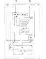
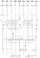
- FIG. 3 is a timing chart showing a method for setting a 3D mode gradation potential (corresponding to gradation A) in Example 1; 1 is a block diagram illustrating a configuration of a liquid crystal display device of Example 1.
- FIG. 3 is a timing chart illustrating a method of setting a 2D mode gradation potential (corresponding to gradation A) in the first embodiment.
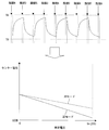
- 6 is a schematic diagram showing one of the effects of Example 1.
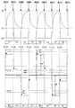
- FIG. 3 is a timing chart illustrating a method of setting a 2D mode gradation potential (corresponding to gradation B ⁇ gradation A) in the first embodiment.
- 3 is a timing chart illustrating a method of setting a 3D mode gradation potential (corresponding to gradation B) in the first embodiment.
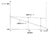
- FIG. 3 is a graph showing effective voltage-center potential characteristics (a function of center potential with respect to effective voltage) in Example 1.
- FIG. 10 is a block diagram illustrating a modification of the liquid crystal display device according to the first embodiment.
- 6 is a graph showing an effective voltage-center potential characteristic (a function of the center potential with respect to the effective voltage) in Example 2.
- 6 is a block diagram illustrating a configuration of a liquid crystal display device according to Embodiment 3.
- FIG. 12 is a timing chart showing a method for setting a gradation potential (corresponding to gradation A) in a non-black insertion mode in Embodiment 3.
- 12 is a timing chart illustrating a method for setting a gradation potential (corresponding to gradation A) in the black insertion mode according to the third embodiment.
- FIG. 10 is a timing chart illustrating a method for setting a gradation potential (corresponding to gradation B) in a non-black insertion mode in Embodiment 3.
- 12 is a timing chart illustrating a method for setting a gradation potential (corresponding to gradation B) in the black insertion mode in the third embodiment.
- 10 is a graph showing effective voltage-center potential characteristics (a function of center potential with respect to gradation) in Example 3.
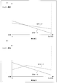
- FIG. 10 is a block diagram illustrating a modification of the liquid crystal display device according to the third embodiment. It is a modification of FIG. It is a modification of FIG. 5 is a graph showing another example of effective voltage-center potential characteristics in Example 1. It is a schematic diagram which shows the transmittance
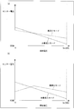
- Example 6 is a graph showing still another example of effective voltage-center potential characteristics in Example 1.
- 10 is a graph showing another example of effective voltage-center potential characteristics in Example 2.
- 10 is a graph showing still another example of effective voltage-center potential characteristics in Example 2.
- FIG. 3 is a reference diagram for explaining Example 1;
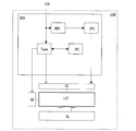
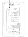
- the present liquid crystal display device LCD includes a liquid crystal panel LCP including data signal lines, scanning signal lines, transistors and pixel electrodes, a backlight BL, and a gate driver for driving the scanning signal lines of the liquid crystal panel LCP. It includes a GD, a source driver SD that drives the data signal lines of the liquid crystal panel LCP, and a display control board DCS (timing controller board) that controls the gate driver and the source driver.
- the display control board DCS includes a timing controller Tcon, a video processing circuit IPC, a 2D-3D display determination circuit DDC, and a driver power supply circuit DPC.
- the timing controller Tcon generates display data and various synchronization signals from the video data IDA in cooperation with the video processing circuit IPC, and outputs them to the gate driver GD and the source driver SD.
- the 2D-3D display determination circuit DDC determines whether it is 2D (2D view) video data or 3D (3D view) video data based on the input video data IDA, and uses the determination result as a driver power supply circuit. Output to DPC.
- the driver power supply circuit DPC supplies a 2D driver power supply voltage to the source driver if it is 2D video data, and supplies a 3D driver power supply voltage to the source driver if it is 3D video data.
- the source driver generates a 2D mode gradation potential using the 2D driver power supply voltage, or generates a 3D mode gradation potential using the 3D driver power supply voltage.
- Cgd is a gate-drain parasitic capacitance
- Clc is a (liquid crystal) capacitance value when the liquid crystal has a transmittance corresponding to the gradation A
- Ccs is an auxiliary (storage) capacitance
- VGH is a scanning signal line.
- An active potential, VGL is an inactive potential of the scanning signal line. It is assumed that the capacitance value when the liquid crystal has a transmittance corresponding to the gradation A (large)> the capacitance value when the liquid crystal has the transmittance corresponding to the black gradation (small). .
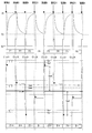
- the liquid crystal has a transmittance TA corresponding to the gradation A, and the gate pulse Gp supplied to the scanning signal line is The pull-in voltage ⁇ VA is generated each time it falls. Since the capacitance value Clc when the liquid crystal has a transmittance corresponding to the gradation A is large, the pull-in voltage ⁇ VA is small, and the intermediate potential (center potential) between VA + and VA ⁇ is VAm. It has become. In the 2D mode, the polarity of the gradation potential is inverted in units of frames.
- the inventor has found that when the gradation A is displayed over a plurality of frames in the 3D mode while the gradation potential of the 2D mode (FIG. 3) is set, a problem as shown in FIG. 24 occurs. That is, in the 3D mode, black gradation (gradation 0) is displayed every other frame in order to avoid mixed viewing of the left and right images. Therefore, when writing of the gradation potential corresponding to gradation A is completed, the liquid crystal is displayed. Is considered to be about the transmittance corresponding to the gradation 0 (not the gradation A) (capacitance value Clc is small), and the actual pull-in voltage becomes considerably larger than ⁇ VA.
- the effective voltage VY of the negative electrode applied to the liquid crystal becomes the effective voltage of the positive electrode.
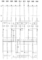
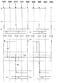
- Example 1 the gradation potential for gradation A in the 3D mode is set as shown in FIG. That is, when the writing of the gradation potential corresponding to the gradation A is completed, the liquid crystal is considered to have about the transmittance corresponding to the gradation 0 (not the gradation A) (capacitance value Clc is small). Make the voltage likelihood greater than ⁇ VA.
- the pull-in voltage ⁇ V0 Cgd / ⁇ (Clc + Ccs + Cgd + Csd) ⁇ (VGH ⁇ VGL) ⁇ (Clc is a capacitance value when the liquid crystal has a transmittance corresponding to gradation 0 and is relatively small)
- the liquid crystal is considered to have a transmittance corresponding to the gradation A (not the gradation 0) (capacitance value Clc is large). Is less than ⁇ V0.
- the gradation potential VA + ′ on the positive electrode side corresponding to the gradation A in the 3D mode is set higher than VA +
- the gradation potential on the negative electrode side corresponding to the gradation A in the 3D mode (writing) (Potential) VA ⁇ ′ is set higher than VA ⁇
- the center potential VAm ′ for the gradation A in the 3D mode is set higher than the center potential VAm for the gradation A in the 2D mode.
- the left-eye video L is displayed in the first frame F1
- the black video B (including a gray video having the same effect as the black video display) is displayed in the second frame F2
- the right-eye video R is displayed in the frame F3
- the black video B is displayed in the fourth frame F4 (one cycle in four frames)
- the polarity of the gradation potential is inverted in units of cycles.
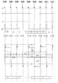
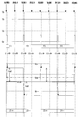
- Example 1 the gradation potential for gradation B ( ⁇ gradation A) in the 2D mode is set as shown in FIG.
- Example 1 the gradation potential for gradation B ( ⁇ gradation A) in the 3D mode is set as shown in FIG. That is, when writing of the gradation potential corresponding to gradation B is completed, the liquid crystal is considered to have a transmittance corresponding to gradation 0 (not gradation B) (capacitance value Clc is small). Make the voltage likelihood greater than ⁇ VB. Further, when the writing of the gradation potential corresponding to gradation 0 is completed, the liquid crystal is considered to have a transmittance corresponding to gradation A (not gradation 0) (capacitance value Clc is large). The potential of the voltage is made smaller than ⁇ V0.
- the positive-side gradation potential VB + ′ corresponding to the gradation A in the 3D mode is set higher than VB +
- the negative-side gradation potential VB ⁇ corresponding to the gradation A in the 3D mode is set.
- the center potential VBm' for gradation B in the 3D mode is set higher than the center potential VBm for gradation B in the 2D mode.
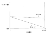
- FIG. 7 shows an example of effective voltage-center potential characteristics in 2D mode (function of center potential with respect to effective voltage) and effective voltage-center potential characteristics in 3D mode (function of center potential with respect to effective voltage).
- the center potential in 3D mode is equal to or higher than the center potential in 2D mode for all effective voltages.
- both the 2D mode and the 3D mode are monotonically decreasing types in which the center potential decreases as the effective voltage increases, it can be seen that the slope of the 3D mode is gentler than that of the 2D mode.
- the driver power supply circuit DPC performs analog switching such as supplying a 2D driver power supply voltage to the source driver or supplying a 3D driver power supply voltage to the source driver.
- a gradation correction circuit GAC is provided on the display control board DCS, and the gradation correction circuit GAC that receives the determination result of the 2D-3D display determination circuit DDC cooperates with the timing controller Tcon. Then, gradation correction in 2D mode or gradation correction in 3D mode may be performed.
- a positive polarity (+) LUT in the 2D mode (look-up table in which the input gradation and the corrected output gradation are associated with each other) is applied to the gradation correction circuit GAC, and the negative polarity ( ⁇ ) in the 2D mode.
- a positive (+) LUT for 3D mode and a negative ( ⁇ ) LUT for 3D mode may be provided.
- the transmittance reaches TA, but depending on the response speed of the liquid crystal, the transmittance often does not reach TA as shown in FIG. Therefore, as shown in FIG. 19, with respect to the effective voltage-center potential characteristic in 2D mode and the effective voltage-center potential characteristic in 3D mode, the slope of 3D mode is made larger than that in FIG. Is desirable.
- the degree of arrival at the 0th gradation is often greatly different between the high gradation (T-Hi) display and the low gradation (T-Lo) display ( In the high gradation, only a gradation much higher than the 0 gradation is reached, but in the low gradation, the vicinity reaches the 0 gradation).
- the center potential for the 0 gradation (black display) effective voltage in the 3D mode is set to be higher than the center potential for the 0 gradation (black display) effective voltage in the 2D mode.
- 3D mode effective voltage-center potential characteristics (monotonically decreasing type) and 2D mode effective voltage-center potential characteristics (monotonically decreasing type) can be set to intersect within the dynamic range of the effective voltage. .
- the center potential for the 0 gradation (black display) effective voltage in the 3D mode is set lower than the center potential for the 0 gradation (black display) effective voltage in the 2D mode.
- Effective voltage-center potential characteristics in 3D mode (monotonically increasing ⁇ monotonically decreasing, the slope changes within the dynamic range of effective voltage) and 2D mode effective voltage-center potential characteristics (monotonically decreasing type) It can also be set to intersect within the dynamic range.
- FIG. 7 relates to a liquid crystal material in which the capacitance value increases (the pull-in voltage decreases) as the gradation (effective voltage to the liquid crystal) increases, but the effective voltage (gradation) increases to the liquid crystal.
- the effective voltage-center potential characteristic in 2D mode and the effective voltage-center in 3D mode for example, as shown in FIG. Potential characteristics can be set.
- the liquid crystal display device LCD includes a liquid crystal panel LCP, a backlight BL, a gate driver GD, a source driver SD, and a display control board DCS (timing controller board).
- the display control board DCS includes a timing controller Tcon, a video processing circuit IPC that performs processing including FRC (frame rate control), and a driver power supply circuit DPC.
- the timing controller Tcon generates display data and various synchronization signals from the video data IDA in cooperation with the video processing circuit IPC, and outputs them to the gate driver GD and the source driver SD.
- the liquid crystal display device LCD of Example 3 is configured so that the user can select a black insertion mode and a non-black insertion mode.
- Black insertion is a technique for reducing the feeling of afterimage when displaying a moving image by periodically displaying black regardless of the input video.
- the driver power supply circuit DPC is supplied with a mode selection signal MCS indicating either the black insertion mode or the non-black insertion mode. If the driver power supply circuit DPC is in the black insertion mode, the driver power supply voltage in the black insertion mode Is supplied to the source driver, and in the non-black insertion mode, the driver power supply voltage in the non-black insertion mode is supplied to the source driver. The source driver uses these driver power supply voltages to generate a gray-scale potential in the black insertion mode or the non-black insertion mode.
- Example 3 the gradation potential for gradation A in the non-black insertion mode is set as shown in FIG.
- the first video F1 is displayed in the first frame F1
- the second video Z2 is displayed in the second frame F2
- the third video Z3 is displayed in the third frame F3.
- the fourth image F4 is displayed in the fourth frame F4, and the polarity of the gradation potential is inverted in units of frames.
- Example 3 the gradation potential for gradation A in the black insertion mode is set as shown in FIG. That is, when writing of the grayscale potential corresponding to the grayscale A is completed, the liquid crystal is considered to have about the transmittance corresponding to the grayscale 0 (not the grayscale B) (capacitance value Clc is small). The potential of the voltage is made larger than the above ⁇ VA. Further, when the writing of the gradation potential corresponding to gradation 0 is completed, the liquid crystal is considered to have a transmittance corresponding to gradation A (not gradation 0) (capacitance value Clc is large). The potential of the voltage is made smaller than the above ⁇ V0.
- the positive-side gradation potential Va + ′ corresponding to the gradation A in the black insertion mode is set higher than Va +
- the negative-side gradation potential corresponding to the gradation A in the black insertion mode is set.
- Va ⁇ ′ is set higher than Va ⁇
- the center potential Vam ′ for the gradation A in the black insertion mode is set higher than the center potential Vam for the gradation A in the non-black insertion mode.
- the first video Z1 is displayed in the first frame F1
- the black video B is displayed in the second frame F2
- the second video Z2 is displayed in the third frame F3.
- the black image B is displayed in the fourth frame F4
- the third image Z3 is displayed in the fifth frame F5
- the black image B is displayed in the sixth frame F6
- the fourth image Z4 is displayed in the seventh frame F7.
- the black image B is displayed in the eighth frame F8, and the polarity of the gradation potential is inverted in units of two frames.
- the burn-in of the liquid crystal can be suppressed in the black insertion mode, and the display with a rough feeling as shown in FIG. 4A can be improved as shown in FIG. .
- Example 3 the gradation potential for gradation B in the black insertion mode is set as shown in FIG. That is, when writing of the gradation potential corresponding to gradation B is completed, the liquid crystal is considered to have a transmittance corresponding to gradation 0 (not gradation B) (capacitance value Clc is small). The potential of the voltage is made larger than the above ⁇ VB. Further, when the writing of the gradation potential corresponding to the gradation 0 is finished, the liquid crystal is considered to have a transmittance (capacitance value Clc large) corresponding to the gradation B (not the gradation 0). The potential of the voltage is made smaller than the above ⁇ V0.
- the positive-side gradation potential Vb + ′ corresponding to the gradation B in the black insertion mode is set higher than Vb +
- the negative-side gradation potential corresponding to the gradation B in the black insertion mode is set.
- Vb ⁇ ′ is set higher than Vb ⁇
- the center potential Vbm ′ for the gradation B in the black insertion mode is set higher than the center potential Vbm for the gradation B in the non-black insertion mode.
- FIG. 15 shows an example of effective voltage-center potential characteristics in the black insertion mode and effective voltage-center potential characteristics in the non-black insertion mode.
- the center potential in the black insertion mode is equal to or higher than the center potential in the non-black insertion mode for all effective voltages.
- the black insertion mode and non-black insertion mode are both monotonically decreasing, with the center potential decreasing as the effective voltage increases.
- the black insertion mode may have a gentler slope than the non-black insertion mode. Recognize.
- the driver power supply circuit DPC performs analog switching in which a driver power supply voltage for non-black insertion is supplied to the source driver or a driver power supply voltage for black insertion is supplied to the source driver. It is not limited to this.
- a gradation correction circuit GAC is provided on the display control board DCS, and the gradation correction circuit receives a mode selection signal MCS indicating either the black insertion mode or the non-black insertion mode.
- the GAC may perform gradation correction in the non-black insertion mode or gradation correction in the black insertion mode in cooperation with the timing controller Tcon.
- the positive polarity (+) LUT in the black insertion mode (look-up table in which the input gradation and the corrected output gradation are associated) is connected to the gradation correction circuit GAC, and the negative polarity in the black insertion mode ( A ⁇ ) LUT, a positive (+) LUT in the non-black insertion mode, and a negative ( ⁇ ) LUT in the non-black insertion mode may be provided.
- the non-black insertion mode in FIG. 11 is 60 Hz driving and the black insertion mode in FIG. 12 is 120 Hz driving, but is not limited thereto.
- the non-black insertion mode may be 60 Hz driving (see FIG. 17), and the black insertion mode may be 240 Hz driving (see FIG. 18).
- the first video W1 is displayed in the first frame F1
- the second video W2 is displayed in the second frame F2
- the third video is displayed in the third frame F3 (not shown).
- the polarity of the gradation potential is inverted in units of frames.
- the first video W1 is displayed in the first frame F1
- the black video B is displayed in the second frame F2
- the first and second videos are displayed in the third frame F3
- the generated interpolated video W1 ′ (in the video processing circuit IPC) is displayed
- the black video B is displayed in the fourth frame F4
- the second video W2 is displayed in the fifth frame F5
- the black is displayed in the sixth frame F6.
- Display the video B display the interpolated video W2 ′ generated from the second and third video (in the video processing circuit IPC) in the seventh frame F7
- the polarity of the gradation potential is inverted every two frames.
- the transmittance reaches TA, but depending on the response speed of the liquid crystal, the transmittance often does not reach TA as shown in FIG. Therefore, as shown in FIG. 22, with respect to the effective voltage-center potential characteristics of the non-black insertion mode and the effective voltage-center potential characteristics of the black insertion mode, the slope of the black insertion mode is increased (as compared to FIG. 15) to It is desirable to approach the inclination of the insertion mode.
- the degree of arrival at the 0th gradation is often greatly different between the high gradation (T-Hi) display and the low gradation (T-Lo) display.
- T-Hi high gradation
- T-Lo low gradation
- the center potential for the zero gradation (black display) effective voltage in the black insertion mode is set to the center potential for the zero gradation (black display) effective voltage in the non-black insertion mode.
- the effective voltage-center potential characteristics (monotonic decrease type) of the black insertion mode and the effective voltage-center potential characteristics (monotonic decrease type) of the non-black insertion mode intersect within the effective voltage dynamic range. Can also be set. Further, as shown in FIG. 23B, the center potential with respect to the 0 gradation (black display) effective voltage in the black insertion mode is determined from the center potential with respect to the 0 gradation (black display) effective voltage in the non-black insertion mode.
- the effective voltage-center potential characteristics of the black insertion mode (monotonically increasing ⁇ monotonically decreasing, the slope changes within the dynamic range of the effective voltage) and the non-black inserting mode effective voltage-center potential characteristics (monotonically decreasing type) ) can also be set to intersect within the dynamic range of the effective voltage.
- the present liquid crystal display device includes a data signal line, a scanning signal line, and a pixel electrode, and applies a plurality of effective voltages to the liquid crystal of the pixel, and applies a single effective voltage to the liquid crystal.
- the effective voltage-center potential characteristic in the second mode is different from the effective voltage-center potential characteristic in the second mode in which specific display is not performed as in the first mode.
- the one effective voltage may be a half of the difference between the positive electrode side potential and the negative electrode side potential.
- the specific display may be a black display.
- the center potential in the first mode is greater than or equal to the center potential in the second mode for each of the plurality of effective voltages, or the center potential in the first mode for each of the plurality of effective voltages is It can also be set as the structure below the center electric potential in 2 modes.
- the effective voltage-center potential characteristic in the second mode (at least a part of the dynamic range of the effective voltage) is monotonically decreasing, and the effective voltage-center potential characteristic in the first mode (of the above dynamic range). Is partly monotonically decreasing than the second mode, or the effective voltage-center potential characteristic in the second mode (at least part of the dynamic range of the effective voltage) is monotonically increasing.
- a configuration in which the effective voltage-center potential characteristic (part of the dynamic range) in the first mode is a monotonically increasing type that is gentler than that in the second mode may be employed.
- the effective voltage corresponding to black display is included in the plurality of effective voltages, Regarding the effective voltage corresponding to the black display, the center potential in the first mode and the center potential in the second mode may be substantially equal.
- the specific display may be performed every n frame periods (n is an integer of 1 to 10).
- the first mode may be a stereoscopic mode and the second mode may be a planar mode.
- the first mode may be a moving image mode and the second mode may be a normal mode.
- the driving method of the present liquid crystal display device is a driving method of a liquid crystal display device that includes a data signal line, a scanning signal line, and a pixel electrode, and applies a plurality of effective voltages to the liquid crystal of the pixel, and applies one effective voltage to the liquid crystal.
- the present invention is not limited to the above-described embodiments, and those obtained by appropriately modifying the above-described embodiments based on common general technical knowledge and those obtained by combining them are also included in the embodiments of the present invention.
- the present invention is suitable for a liquid crystal TV and a liquid crystal display.
- a gradation B gradation Clc Liquid crystal capacity (value) VCOM Common electrode potential VeA Effective voltage VeB (to liquid crystal corresponding to gradation A) Effective voltage VeB (To liquid crystal corresponding to gradation B) F1 to F8 First to eighth frames VAm (2D mode gradation) Center potential VAm ′ (for gradation A in 3D mode) Center potential VBm (for gradation B in 2D mode) Center potential VBm ′ (for gradation B in 3D mode) Center potential Vam (for black) Center potential Vam ′ (for gradation A in the insertion mode) Center potential (for gradation A in the black insertion mode) L Left-eye image R Right-eye image B Black image TA Liquid crystal transmittance corresponding to gradation A TB Transmittance of liquid crystal corresponding to gradation A T0 Transmittance of liquid crystal corresponding to gradation 0 (black gradation) Gp Gate pulse
Landscapes
- Engineering & Computer Science (AREA)
- Chemical & Material Sciences (AREA)
- Crystallography & Structural Chemistry (AREA)
- Physics & Mathematics (AREA)
- Computer Hardware Design (AREA)
- General Physics & Mathematics (AREA)
- Theoretical Computer Science (AREA)
- Control Of Indicators Other Than Cathode Ray Tubes (AREA)
Abstract
本液晶表示装置は、データ信号線および走査信号線並びに画素電極を備え、画素の液晶に複数の実効電圧をにかける液晶表示装置であって、1つの実効電圧を液晶にかけるときにデータ信号線に供給される正極側電位および負極側電位の中間値をこの1つの実効電圧に対するセンター電位とし、周期的に特定の表示を行う第1モードにおける実効電圧-センター電位特性を、第1モードのような特定の表示を行わない第2モードにおける実効電圧-センター電位特性とは異ならせている。こうすれば、周期的に特定の表示を行う液晶表示装置の表示不良が改善される。
Description
本発明は、液晶表示装置の駆動技術に関する。
特許文献1には、一定期間ごとに特定の表示(例えば、黒表示)を行うことで、動画表示時の残像感を低減する技術が開示され、特許文献2には、いわゆる3D表示時に、一定期間ごとに特定の表示(例えば、黒表示)を行うことで、右眼用映像と左眼用映像が混在視されないようにする技術が開示されている。
液晶表示装置においては、(薄膜)トランジスタがOFF(トランジスタが接続される走査信号線の電位がHighからLowに移行)するときに、トランジスタのゲート電極および画素電極間の寄生容量に起因して、画素電極に書き込まれた階調電位が引き込まれる現象(いわゆる引き込み電圧)が生じる。引き込み電圧は液晶容量の値に依存し、液晶容量の値は液晶容量にかかる電圧に依存しているため、引き込み電圧は階調依存性を有する。そこで、液晶表示装置では、階調に応じて引き込み電圧を見積もり、この引き込み電圧を考慮して階調電位を設定する引き込み電圧補正が一般的に行われている。
発明者は、上記のように周期的に特定の表示を行う場合に、引き込み電圧に起因する表示不良が生じることを見出した。
本発明の目的の1つは、周期的に特定の表示を行う液晶表示装置の表示不良を改善することにある。
本液晶表示装置は、データ信号線および走査信号線並びに画素電極を備え、画素の液晶に複数の実効電圧をかける液晶表示装置であって、1つの実効電圧を液晶にかけるときにデータ信号線に供給される正極側電位および負極側電位の中間値をこの1つの実効電圧に対するセンター電位とし、周期的に特定の表示を行う(周期的に特定映像を挿入する)第1モードにおける実効電圧-センター電位特性を、第1モードのような特定の表示を行わない第2モードにおける実効電圧-センター電位特性とは異ならせたものである。
周期的に特定の表示を行う液晶表示装置の表示不良を改善することができる。
〔実施例1〕
図2に示すように、本液晶表示装置LCDは、データ信号線、走査信号線、トランジスタおよび画素電極を含む液晶パネルLCPと、バックライトBLと、液晶パネルLCPの走査信号線を駆動するゲートドライバGDと、液晶パネルLCPのデータ信号線を駆動するソースドライバSDと、ゲートドライバおよびソースドライバを制御する表示制御基板DCS(タイミングコントローラ基板)とを備える。表示制御基板DCSは、タイミングコントローラTcon、映像処理回路IPC、2D-3D表示判定回路DDC、およびドライバ電源回路DPCを含む。タイミングコントローラTconは、映像処理回路IPCと協働して映像データIDAから表示データおよび各種同期信号を生成し、これらをゲートドライバGDおよびソースドライバSDに出力する。
図2に示すように、本液晶表示装置LCDは、データ信号線、走査信号線、トランジスタおよび画素電極を含む液晶パネルLCPと、バックライトBLと、液晶パネルLCPの走査信号線を駆動するゲートドライバGDと、液晶パネルLCPのデータ信号線を駆動するソースドライバSDと、ゲートドライバおよびソースドライバを制御する表示制御基板DCS(タイミングコントローラ基板)とを備える。表示制御基板DCSは、タイミングコントローラTcon、映像処理回路IPC、2D-3D表示判定回路DDC、およびドライバ電源回路DPCを含む。タイミングコントローラTconは、映像処理回路IPCと協働して映像データIDAから表示データおよび各種同期信号を生成し、これらをゲートドライバGDおよびソースドライバSDに出力する。
2D-3D表示判定回路DDCは、入力される映像データIDAに基づいて2D(2次元視)用の映像データか3D(3次元視)用の映像データかを判別し、判別結果をドライバ電源回路DPCに出力する。ドライバ電源回路DPCは、2D用の映像データであれば、2D用のドライバ電源電圧をソースドライバに供給し、3D用の映像データであれば、3D用のドライバ電源電圧をソースドライバに供給する。ソースドライバは、2D用のドライバ電源電圧を用いて2Dモードの階調電位を生成するか、あるいは3D用のドライバ電源電圧を用いて3Dモードの階調電位を生成する。
実施例1では、2Dモードでの階調Aに対する階調電位を図3のように設定している。すなわち、共通(対向)電極の電位をVCOMとし、階調Aに対応する液晶への実効電圧(共通電極と画素電極の間の実効電圧)をVeA(>0)とし、引き込み電圧をΔVA=Cgd/{(Clc+Ccs+Cgd+Csd)×(VGH-VGL)}とし、階調Aに対応する正極側の階調電位(書き込み電位)VA+を、VA+=VCOM+VeA+ΔVAと設定し、負極側の階調電位VA-を、VA-=VCOM-VeA+ΔVAと設定する。なお、Cgdはゲートードレイン間寄生容量、Clcは、液晶が階調Aに対応する透過率になっているときの(液晶)容量値、Ccsは補助(蓄積)容量、VGHは走査信号線のアクティブ電位、VGLは走査信号線の非アクティブ電位である。なお、液晶が階調Aに対応する透過率になっているときの容量値(大)>液晶が黒階調に対応する透過率になっているときの容量値(小)であるものとする。
図3に示すように、2Dモードで複数フレームに亘って階調Aを表示するときには、液晶が階調Aに対応する透過率TAとなっており、走査信号線に供給されるゲートパルスGpが立ち下がるたびに上記引き込み電圧ΔVAが生じる。なお、液晶が階調Aに対応する透過率になっているときの容量値Clcは大であるため、引き込み電圧ΔVAは小さくなっており、VA+とVA-の中間電位(センター電位)はVAmとなっている。なお、2Dモードでは、フレーム単位で階調電位の極性を反転させている。
発明者は、2Dモードの階調電位(図3)に設定したまま、3Dモードで複数フレームに亘って階調Aを表示すると、図24のような不具合が起こることを見出した。すなわち、3Dモードでは、左右の映像の混在視を避けるべく1フレームおきに黒階調(階調0)を表示するため、階調Aに対応する階調電位の書き込みが終了したときに、液晶は、(階調Aではなく)階調0に対応する透過率程度(容量値Clc小)と考えられ、実際の引き込み電圧がΔVAよりもかなり大きくなる。したがって、2Dモードの階調電位の設定(VA+=VCOM+VeA+ΔVA、VA-=VCOM-VeA+ΔVA、センター電位VAm)のままだと、図24に示すように、液晶にかかる負極の実効電圧VYが正極の実効電圧VXよりも大きくなり、DC印加により液晶が焼き付いたり、実効電圧の差によって図4(a)のような市松状のざらつき感がでたりする。
実施例1では、3Dモードでの階調Aに対する階調電位を図1のように設定している。すなわち、階調Aに対応する階調電位の書き込みが終了したときに、液晶は、(階調Aではなく)階調0に対応する透過率程度(容量値Clc小)と考えられるため、引き込み電圧の見込みをΔVAよりも大きくする。また、引き込み電圧ΔV0=Cgd/{(Clc+Ccs+Cgd+Csd)×(VGH-VGL)}として(Clcは、液晶が階調0に対応する透過率になっているときの容量値であり、相対的に小さい)、階調0に対応する階調電位の書き込みが終了したときに、液晶は、(階調0ではなく)階調Aに対応する透過率程度(容量値Clc大)と考えられるため、引き込み電圧の見込みをΔV0よりも小さくする。具体的には、3Dモードでの階調Aに対応する正極側の階調電位VA+’を、VA+よりも高く設定し、3Dモードでの階調Aに対応する負極側の階調電位(書き込み電位)VA-’を、VA-よりも高く設定し、3Dモードでの階調Aに対するセンター電位VAm’を2Dモードでの階調Aに対するセンター電位VAmよりも高くする。
図1のような設定を行うことで、3Dモードにおいて、液晶の焼き付き付きを抑え、図4(a)のようなざらつき感のある表示を図4(b)のように改善することができる。
なお、3Dモードでは、第1フレームF1で左眼用映像Lを表示し、第2フレームF2で黒映像B(黒映像表示と同程度の効果を奏するグレー映像を含む)を表示し、第3フレームF3で右眼用映像Rを表示し、第4フレームF4で黒映像Bを表示し(4フレームで1周期)、周期単位で階調電位の極性を反転させている。
実施例1では、2Dモードでの階調B(<階調A)に対する階調電位を図5のように設定している。階調Bに対応する液晶への実効電圧(共通電極と画素電極の間の実効電圧)をVeB(>0)とし、引き込み電圧をΔVB=Cgd/{(Clc+Ccs+Cgd+Csd)×(VGH-VGL)}とし(Clcは、液晶が階調Bに対応する透過率になっているときの容量値であり、相対的に中ぐらい)、階調Bに対応する正極側の階調電位(書き込み電位)VB+を、VB+=VCOM+VeB+ΔVBと設定し、負極側の階調電位VB-を、VB-=VCOM-VeB+ΔVBと設定し、VB+とVB-の中間電位(センター電位)をVBmとしている。なお、センター電位VBm>センター電位VAmとなっている。
実施例1では、3Dモードでの階調B(<階調A)に対する階調電位を図6のように設定している。すなわち、階調Bに対応する階調電位の書き込みが終了したときに、液晶は、(階調Bではなく)階調0に対応する透過率程度(容量値Clc小)と考えられるため、引き込み電圧の見込みをΔVBよりも大きくする。また、階調0に対応する階調電位の書き込みが終了したときに、液晶は、(階調0ではなく)階調Aに対応する透過率程度(容量値Clc大)と考えられるため、引き込み電圧の見込みをΔV0よりも小さくする。具体的には、3Dモードでの階調Aに対応する正極側の階調電位VB+’を、VB+よりも高く設定し、3Dモードでの階調Aに対応する負極側の階調電位VB-’を、VB-よりも高く設定し、3Dモードでの階調Bに対するセンター電位VBm’を2Dモードでの階調Bに対するセンター電位VBmよりも高くする。なお、センター電位VBm’≒センター電位VAm’となっている。
図7に、2Dモードにおける実効電圧-センター電位特性(実効電圧に対するセンター電位の関数)および3Dモードにおける実効電圧-センター電位特性(実効電圧に対するセンター電位の関数)の一例を示す。3Dモードのセンター電位は、すべての実効電圧について2Dモードのセンター電位以上となっている。また、2Dモードおよび3Dモードともに実効電圧の増加に伴ってセンター電位が低下する単調減少型であるが、3Dモードは、2Dモードに比較して傾きが緩やかであることがわかる。
図2では、ドライバ電源回路DPCが、2D用のドライバ電源電圧をソースドライバに供給したり、3D用のドライバ電源電圧をソースドライバに供給したりするアナログ的な切り替えを行っているがこれに限定されない。例えば、図8に示すように、表示制御基板DCSに階調補正回路GACを設けておき、2D-3D表示判定回路DDCの判定結果を受けた階調補正回路GACが、タイミングコントローラTconと協働して2Dモードの階調補正あるいは3Dモードの階調補正を行ってもよい。この場合、階調補正回路GACに、2Dモードでの正極性(+)用LUT(入力階調と補正後の出力階調を対応付けたルックアップテーブル)、2Dモードでの負極性(-)用LUT、3Dモードでの正極性(+)用LUT、および3Dモードでの負極性(-)用LUTを設けてもよい。
図1では、透過率がTAまで到達しているが、液晶の応答速度によっては、図19に示すように透過率がTAまで到達しない場合も多い。そこで、図19に示すように、2Dモードの実効電圧-センター電位特性および3Dモードの実効電圧-センター電位特性について、3Dモードの傾きを(図7よりも)大きくし、2Dモードの傾きに近づけるのが望ましい。
また、3Dモードでは、図20に示すように、高階調(T-Hi)の表示と低階調(T-Lo)の表示とでは、0階調への到達度合いが大きく異なることも多い(高階調では0階調よりもかなり高い階調までしか到達しないが、低階調では0階調付近まで到達する)。この場合は、図21(a)に示すように、3Dモードでの0階調(黒表示)実効電圧に対するセンター電位を、2Dモードでの0階調(黒表示)実効電圧に対するセンター電位よりも低くし、3Dモードの実効電圧-センター電位特性(単調減少型)と2Dモードの実効電圧-センター電位特性(単調減少型)とが、実効電圧のダイナミックレンジ内で交わるように設定することもできる。また、図21(b)に示すように、3Dモードでの0階調(黒表示)実効電圧に対するセンター電位を、2Dモードでの0階調(黒表示)実効電圧に対するセンター電位よりも低くし、3Dモードの実効電圧-センター電位特性(単調増加→単調減少へと、実効電圧のダイナミックレンジ内で傾きが変わる)と2Dモードの実効電圧-センター電位特性(単調減少型)とが、実効電圧のダイナミックレンジ内で交わるように設定することもできる。
〔実施例2〕
図7は、階調(液晶への実効電圧)の増加に伴って容量値が大きくなる(引き込み電圧は小さくなる)液晶材についてのものであるが、液晶への実効電圧(階調)の増加に伴って容量値が小さくなる(引き込み電圧は大きくなる)ような液晶材を用いた場合には、例えば図9のように、2Dモードにおける実効電圧-センター電位特性および3Dモードにおける実効電圧-センター電位特性を設定することができる。
図7は、階調(液晶への実効電圧)の増加に伴って容量値が大きくなる(引き込み電圧は小さくなる)液晶材についてのものであるが、液晶への実効電圧(階調)の増加に伴って容量値が小さくなる(引き込み電圧は大きくなる)ような液晶材を用いた場合には、例えば図9のように、2Dモードにおける実効電圧-センター電位特性および3Dモードにおける実効電圧-センター電位特性を設定することができる。
〔実施例3〕
実施例3の液晶表示装置LCDは、図10に示すように、液晶パネルLCPと、バックライトBLと、ゲートドライバGDと、ソースドライバSDと、表示制御基板DCS(タイミングコントローラ基板)とを備える。表示制御基板DCSは、タイミングコントローラTcon、FRC(フレームレートコントロール)を含む処理を行う映像処理回路IPC、およびドライバ電源回路DPCを含む。タイミングコントローラTconは、映像処理回路IPCと協働して映像データIDAから表示データおよび各種同期信号を生成し、これらをゲートドライバGDおよびソースドライバSDに出力する。
実施例3の液晶表示装置LCDは、図10に示すように、液晶パネルLCPと、バックライトBLと、ゲートドライバGDと、ソースドライバSDと、表示制御基板DCS(タイミングコントローラ基板)とを備える。表示制御基板DCSは、タイミングコントローラTcon、FRC(フレームレートコントロール)を含む処理を行う映像処理回路IPC、およびドライバ電源回路DPCを含む。タイミングコントローラTconは、映像処理回路IPCと協働して映像データIDAから表示データおよび各種同期信号を生成し、これらをゲートドライバGDおよびソースドライバSDに出力する。
実施例3の液晶表示装置LCDは、黒挿入モードと非黒挿入モードとをユーザが選択できるように構成されている。なお、黒挿入とは、入力映像とは関係なく周期的に黒表示を行うことで、動画表示時の残像感を低減する技術である。
ドライバ電源回路DPCには、黒挿入モードおよび非黒挿入モードのいずれのモードかを示すモード選択信号MCSが入力され、ドライバ電源回路DPCは、黒挿入モードであれば、黒挿入モードのドライバ電源電圧をソースドライバに供給し、非黒挿入モードであれば、非黒挿入モードのドライバ電源電圧をソースドライバに供給する。ソースドライバは、これらドライバ電源電圧を用いて、黒挿入モードあるいは非黒挿入モードの階調電位を生成する。
実施例3では、非黒挿入モードでの階調Aに対する階調電位を図11のように設定している。すなわち、階調Aに対応する正極側の階調電位(書き込み電位)Va+を、Va+=VCOM+VeA+ΔVAと設定し(実施例1参照)、負極側の階調電位Va-を、Va-=VCOM-VeA+ΔVAと設定し(実施例1参照)、Va+とVa-の中間電位(センター電位)をVam(=実施例1のVAm)としている。
なお、非黒挿入モード(例えば、60Hz駆動)では、第1フレームF1で第1映像Z1を表示し、第2フレームF2で第2映像Z2を表示し、第3フレームF3で第3映像Z3を表示し、第4フレームF4で第4映像Z4を表示し、フレーム単位で階調電位の極性を反転させている。
実施例3では、黒挿入モードでの階調Aに対する階調電位を図12のように設定している。すなわち、階調Aに対応する階調電位の書き込みが終了したときに、液晶は、(階調Bではなく)階調0に対応する透過率程度(容量値Clc小)と考えられるため、引き込み電圧の見込みを上記ΔVAよりも大きくする。また、階調0に対応する階調電位の書き込みが終了したときに、液晶は、(階調0ではなく)階調Aに対応する透過率程度(容量値Clc大)と考えられるため、引き込み電圧の見込みを上記ΔV0よりも小さくする。具体的には、黒挿入モードでの階調Aに対応する正極側の階調電位Va+’を、Va+よりも高く設定し、黒挿入モードでの階調Aに対応する負極側の階調電位Va-’を、Va-よりも高く設定し、黒挿入モードでの階調Aに対するセンター電位Vam’を、非黒挿入モードでの階調Aに対するセンター電位Vamよりも高くする。
なお、黒挿入モード(例えば、120Hz駆動)では、第1フレームF1で第1映像Z1を表示し、第2フレームF2で黒映像Bを表示し、第3フレームF3で第2映像Z2を表示し、第4フレームF4で黒映像Bを表示し、第5フレームF5で第3映像Z3を表示し、第6フレームF6で黒映像Bを表示し、第7フレームF7で第4映像Z4を表示し、第8フレームF8で黒映像Bを表示し、2フレーム単位で階調電位の極性を反転させている。
図12のような設定を行うことで、黒挿入モードにおいて、液晶の焼き付き付きを抑え、図4(a)のようなざらつき感のある表示を図4(b)のように改善することができる。
実施例3では、非黒挿入モードでの階調Bに対する階調電位を図13のように設定している。すなわち、階調Bに対応する正極側の階調電位(書き込み電位)Vb+を、Vb+=VCOM+VeB+ΔVBと設定し(実施例1参照)、負極側の階調電位Vb-を、Vb-=VCOM-VeB+ΔVBと設定し(実施例1参照)、Vb+とVb-の中間電位(センター電位)をVbm(=実施例1のVBm)としている。
実施例3では、黒挿入モードでの階調Bに対する階調電位を図14のように設定している。すなわち、階調Bに対応する階調電位の書き込みが終了したときに、液晶は、(階調Bではなく)階調0に対応する透過率程度(容量値Clc小)と考えられるため、引き込み電圧の見込みを上記ΔVBよりも大きくする。また、階調0に対応する階調電位の書き込みが終了したときに、液晶は、(階調0ではなく)階調Bに対応する透過率程度(容量値Clc大)と考えられるため、引き込み電圧の見込みを上記ΔV0よりも小さくする。具体的には、黒挿入モードでの階調Bに対応する正極側の階調電位Vb+’を、Vb+よりも高く設定し、黒挿入モードでの階調Bに対応する負極側の階調電位Vb-’を、Vb-よりも高く設定し、黒挿入モードでの階調Bに対するセンター電位Vbm’を、非黒挿入モードでの階調Bに対するセンター電位Vbmよりも高くする。
図15に、黒挿入モードにおける実効電圧-センター電位特性および非黒挿入モードにおける実効電圧-センター電位特性の一例を示す。黒挿入モードのセンター電位は、すべての実効電圧について非黒挿入モードのセンター電位以上となっている。また、黒挿入モードおよび非黒挿入モードともに実効電圧の増加に伴ってセンター電位が低下する単調減少型であるが、黒挿入モードは、非黒挿入モードに比較して傾きが緩やかであることがわかる。
図10では、ドライバ電源回路DPCが、非黒挿入用のドライバ電源電圧をソースドライバに供給したり、黒挿入用のドライバ電源電圧をソースドライバに供給したりするアナログ的な切り替えを行っているがこれに限定されない。例えば、図16に示すように、表示制御基板DCSに階調補正回路GACを設けておき、黒挿入モードおよび非黒挿入モードのいずれのモードかを示すモード選択信号MCSを受けた階調補正回路GACが、タイミングコントローラTconと協働して非黒挿入モードの階調補正あるいは黒挿入モードの階調補正を行ってもよい。この場合、階調補正回路GACに、黒挿入モードでの正極性(+)用LUT(入力階調と補正後の出力階調を対応付けたルックアップテーブル)、黒挿入モードでの負極性(-)用LUT、非黒挿入モードでの正極性(+)用LUT、および非黒挿入モードでの負極性(-)用LUTを設けてもよい。
図11の非黒挿入モードは60Hz駆動で、図12の黒挿入モードは120Hz駆動としているがこれに限定されない。たとえば、非黒挿入モードは60Hz駆動で(図17参照)、黒挿入モードは240Hz駆動(図18参照)とすることもできる。
図17の非黒挿入モード(60Hz駆動)では、第1フレームF1で第1映像W1を表示し、第2フレームF2で第2映像W2を表示し、図示しない第3フレームF3で第3映像を表示し、フレーム単位で階調電位の極性を反転させている。
図18の黒挿入モード(240Hz駆動)では、第1フレームF1で第1映像W1を表示し、第2フレームF2で黒映像Bを表示し、第3フレームF3で第1および第2映像から(映像処理回路IPCにて)生成された挿間映像W1’を表示し、第4フレームF4で黒映像Bを表示し、第5フレームF5で第2映像W2を表示し、第6フレームF6で黒映像Bを表示し、第7フレームF7で第2および第3映像から(映像処理回路IPCにて)生成された挿間映像W2’を表示し、第8フレームF8で黒映像Bを表示し、2フレーム単位で階調電位の極性を反転させている。
図12では、透過率がTAまで到達しているが、液晶の応答速度によっては、図22に示すように透過率がTAまで到達しない場合も多い。そこで、図22に示すように、非黒挿入モードの実効電圧-センター電位特性および黒挿入モードの実効電圧-センター電位特性について、黒挿入モードの傾きを(図15よりも)大きくし、非黒挿入モードの傾きに近づけるのが望ましい。
また、黒挿入モードでは、図20に示すように、高階調(T-Hi)の表示と低階調(T-Lo)の表示とでは、0階調への到達度合いが大きく異なることも多い(高階調では0階調よりもかなり高い階調までしか到達しないが、低階調では0階調付近まで到達する)。この場合は、図23(a)に示すように、黒挿入モードでの0階調(黒表示)実効電圧に対するセンター電位を、非黒挿入モードでの0階調(黒表示)実効電圧に対するセンター電位よりも低くし、黒挿入モードの実効電圧-センター電位特性(単調減少型)と非黒挿入モードの実効電圧-センター電位特性(単調減少型)とが、実効電圧のダイナミックレンジ内で交わるように設定することもできる。また、図23(b)に示すように、黒挿入モードでの0階調(黒表示)実効電圧に対するセンター電位を、非黒挿入モードでの0階調(黒表示)実効電圧に対するセンター電位よりも低くし、黒挿入モードの実効電圧-センター電位特性(単調増加→単調減少へと、実効電圧のダイナミックレンジ内で傾きが変わる)と非黒挿入モードの実効電圧-センター電位特性(単調減少型)とが、実効電圧のダイナミックレンジ内で交わるように設定することもできる。
以上のように、本液晶表示装置は、データ信号線および走査信号線並びに画素電極を備え、画素の液晶に複数の実効電圧をかける液晶表示装置であって、1つの実効電圧を液晶にかけるときにデータ信号線に供給される正極側電位および負極側電位の中間値をこの1つの実効電圧に対するセンター電位とし、周期的に特定の表示を行う(周期的に特定映像を挿入する)第1モードにおける実効電圧-センター電位特性を、第1モードのような特定の表示を行わない第2モードにおける実効電圧-センター電位特性とは異ならせたものである。
上記構成によれば、周期的に特定の表示を行う液晶表示装置の表示不良を改善することができる。
本液晶表示装置では、上記1つの実効電圧は、上記正極側電位および負極側電位の差の半分である構成とすることもできる。
本液晶表示装置では、上記特定の表示が黒表示である構成とすることもできる。
本液晶表示装置では、複数の実効電圧それぞれについて、第1モードにおけるセンター電位が、第2モードにおけるセンター電位以上であるか、あるいは、複数の実効電圧それぞれについて、第1モードにおけるセンター電位が、第2モードにおけるセンター電位以下である構成とすることもできる。
本液晶表示装置では、第2モードにおける実効電圧-センター電位特性(少なくとも実効電圧のダイナミックレンジの一部)が単調減少型であるとともに、第1モードにおける実効電圧-センター電位特性(上記ダイナミックレンジの一部)が第2モードよりも緩やかな単調減少型であるか、あるいは、第2モードにおける実効電圧-センター電位特性(少なくとも実効電圧のダイナミックレンジの一部)が単調増加型であるとともに、第1モードにおける実効電圧-センター電位特性(上記ダイナミックレンジの一部)が第2モードよりも緩やかな単調増加型である構成とすることもできる。
本液晶表示装置では、上記複数の実効電圧に、黒表示に対応する実効電圧が含まれ、
黒表示に対応する実効電圧については、第1モードにおけるセンター電位と、第2モードにおけるセンター電位とが実質的に等しい構成とすることもできる。
黒表示に対応する実効電圧については、第1モードにおけるセンター電位と、第2モードにおけるセンター電位とが実質的に等しい構成とすることもできる。
本液晶表示装置では、nフレーム期間(nは1以上10以下の整数)ごとに上記特定の表示を行う構成とすることもできる。
本液晶表示装置では、第1モードは立体視モードであり、第2モードは平面視モードである構成とすることもできる。
本液晶表示装置では、第1モードは動画モードであり、第2モードは通常モードである構成とすることもできる。
本液晶表示装置の駆動方法は、データ信号線および走査信号線並びに画素電極を備え、画素の液晶に複数の実効電圧をかける液晶表示装置の駆動方法であって、1つの実効電圧を液晶にかけるときにデータ信号線に供給される正極側電位および負極側電位の中間値をこの1つの実効電圧に対するセンター電位として、周期的に特定の表示を行う第1モードにおける実効電圧-センター電位特性を、第1モードのような特定の表示を行わない第2モードにおける実効電圧-センター電位特性とは異ならせるものである。
本発明は上記の実施の形態に限定されるものではなく、上記実施の形態を技術常識に基づいて適宜変更したものやそれらを組み合わせて得られるものも本発明の実施の形態に含まれる。
本発明は、液晶TVや液晶ディスプレイに好適である。
A 階調
B 階調
Clc 液晶容量(値)
VCOM 共通電極の電位
VeA (階調Aに対応する液晶への)実効電圧
VeB (階調Bに対応する液晶への)実効電圧
F1~F8 第1~第8フレーム
VAm (2Dモードでの階調Aに対する)センター電位
VAm’ (3Dモードでの階調Aに対する)センター電位
VBm (2Dモードでの階調Bに対する)センター電位
VBm’ (3Dモードでの階調Bに対する)センター電位
Vam (非黒挿入モードでの階調Aに対する)センター電位
Vam’ (黒挿入モードでの階調Aに対する)センター電位
L 左眼用映像
R 右眼用映像
B 黒映像
TA 階調Aに対応する液晶の透過率
TB 階調Aに対応する液晶の透過率
T0 階調0(黒階調)に対応する液晶の透過率
Gp ゲートパルス
B 階調
Clc 液晶容量(値)
VCOM 共通電極の電位
VeA (階調Aに対応する液晶への)実効電圧
VeB (階調Bに対応する液晶への)実効電圧
F1~F8 第1~第8フレーム
VAm (2Dモードでの階調Aに対する)センター電位
VAm’ (3Dモードでの階調Aに対する)センター電位
VBm (2Dモードでの階調Bに対する)センター電位
VBm’ (3Dモードでの階調Bに対する)センター電位
Vam (非黒挿入モードでの階調Aに対する)センター電位
Vam’ (黒挿入モードでの階調Aに対する)センター電位
L 左眼用映像
R 右眼用映像
B 黒映像
TA 階調Aに対応する液晶の透過率
TB 階調Aに対応する液晶の透過率
T0 階調0(黒階調)に対応する液晶の透過率
Gp ゲートパルス
Claims (18)
- データ信号線および走査信号線並びに画素電極を備え、画素の液晶に複数の実効電圧をかける液晶表示装置であって、
1つの実効電圧を液晶にかけるときにデータ信号線に供給される正極側電位および負極側電位の中間値をこの1つの実効電圧に対するセンター電位とし、
周期的に特定の表示を行う第1モードにおける実効電圧-センター電位特性を、第1モードのような特定の表示を行わない第2モードにおける実効電圧-センター電位特性とは異ならせた液晶表示装置。 - 上記1つの実効電圧は、上記正極側電位および負極側電位の差の半分である請求項1記載の液晶表示装置。
- 上記特定の表示が黒表示である請求項1記載の液晶表示装置。
- 複数の実効電圧それぞれについて、第1モードにおけるセンター電位が、第2モードにおけるセンター電位以上であるか、あるいは、
複数の実効電圧それぞれについて、第1モードにおけるセンター電位が、第2モードにおけるセンター電位以下である請求項1記載の液晶表示装置 - 第2モードにおける実効電圧-センター電位特性が単調減少型であるとともに、第1モードにおける実効電圧-センター電位特性が第2モードよりも緩やかな単調減少型であるか、あるいは、
第2モードにおける実効電圧-センター電位特性が単調増加型であるとともに、第1モードにおける実効電圧-センター電位特性が第2モードよりも緩やかな単調増加型である請求項1記載の液晶表示装置。 - 上記複数の実効電圧に、黒表示に対応する実効電圧が含まれ、
黒表示に対応する実効電圧については、第1モードにおけるセンター電位と、第2モードにおけるセンター電位とが実質的に等しい請求項1記載の液晶表示装置 - nフレーム期間(nは1以上10以下の整数)ごとに上記特定の表示を行う請求項1記載の液晶表示装置。
- 第1モードは立体視モードであり、第2モードは平面視モードである請求項1記載の液晶表示装置。
- 第1モードは動画モードであり、第2モードは通常モードである請求項1記載の液晶表示装置。
- データ信号線および走査信号線並びに画素電極を備え、画素の液晶に複数の実効電圧をかける液晶表示装置の駆動方法であって、
1つの実効電圧を液晶にかけるときにデータ信号線に供給される正極側電位および負極側電位の中間値をこの1つの実効電圧に対するセンター電位として、
周期的に特定の表示を行う第1モードにおける実効電圧-センター電位特性を、第1モードのような特定の表示を行わない第2モードにおける実効電圧-センター電位特性とは異ならせる液晶表示装置の駆動方法。 - 上記1つの実効電圧は、上記正極側電位および負極側電位の差の半分である請求項10記載の液晶表示装置の駆動方法。
- 上記特定の表示が黒表示である請求項10記載の液晶表示装置の駆動方法。
- 複数の実効電圧それぞれについて、第1モードにおけるセンター電位が、第2モードにおけるセンター電位以上であるか、あるいは、
複数の実効電圧それぞれについて、第1モードにおけるセンター電位が、第2モードにおけるセンター電位以下である請求項10記載の液晶表示装置の駆動方法。 - 第2モードにおける実効電圧-センター電位特性が単調減少型であるとともに、第1モードにおける実効電圧-センター電位特性が第2モードよりも緩やかな単調減少型であるか、あるいは、
第2モードにおける実効電圧-センター電位特性が単調増加型であるとともに、第1モードにおける実効電圧-センター電位特性が第2モードよりも緩やかな単調増加型である請求項10記載の液晶表示装置の駆動方法。 - 上記複数の実効電圧に、黒表示に対応する実効電圧が含まれ、
黒表示に対応する実効電圧については、第1モードにおけるセンター電位と、第2モードにおけるセンター電位とが実質的に等しい請求項10記載の液晶表示装置の駆動方法。 - nフレーム期間(nは1以上10以下の整数)ごとに上記特定の表示を行う請求項10記載の液晶表示装置の駆動方法。
- 第1モードは立体視モードであり、第2モードは平面視モードである請求項10記載の液晶表示装置の駆動方法。
- 第1モードは動画モードであり、第2モードは通常モードである請求項10記載の液晶表示装置の駆動方法。
Applications Claiming Priority (2)
| Application Number | Priority Date | Filing Date | Title |
|---|---|---|---|
| JP2011119776 | 2011-05-27 | ||
| JP2011-119776 | 2011-05-27 |
Publications (1)
| Publication Number | Publication Date |
|---|---|
| WO2012165304A1 true WO2012165304A1 (ja) | 2012-12-06 |
Family
ID=47259161
Family Applications (1)
| Application Number | Title | Priority Date | Filing Date |
|---|---|---|---|
| PCT/JP2012/063383 Ceased WO2012165304A1 (ja) | 2011-05-27 | 2012-05-24 | 液晶表示装置、液晶表示装置の駆動方法 |
Country Status (1)
| Country | Link |
|---|---|
| WO (1) | WO2012165304A1 (ja) |
Citations (3)
| Publication number | Priority date | Publication date | Assignee | Title |
|---|---|---|---|---|
| JP2006245924A (ja) * | 2005-03-02 | 2006-09-14 | Funai Electric Co Ltd | 液晶テレビジョン |
| JP2008306335A (ja) * | 2007-06-06 | 2008-12-18 | Sony Corp | 液晶プロジェクタおよび液晶プロジェクタの制御方法 |
| WO2009125600A1 (ja) * | 2008-04-11 | 2009-10-15 | 株式会社ナナオ | 液晶画像表示装置 |
-
2012
- 2012-05-24 WO PCT/JP2012/063383 patent/WO2012165304A1/ja not_active Ceased
Patent Citations (3)
| Publication number | Priority date | Publication date | Assignee | Title |
|---|---|---|---|---|
| JP2006245924A (ja) * | 2005-03-02 | 2006-09-14 | Funai Electric Co Ltd | 液晶テレビジョン |
| JP2008306335A (ja) * | 2007-06-06 | 2008-12-18 | Sony Corp | 液晶プロジェクタおよび液晶プロジェクタの制御方法 |
| WO2009125600A1 (ja) * | 2008-04-11 | 2009-10-15 | 株式会社ナナオ | 液晶画像表示装置 |
Similar Documents
| Publication | Publication Date | Title |
|---|---|---|
| KR102246262B1 (ko) | 표시 패널의 구동 방법 및 이를 수행하기 위한 표시 장치 | |
| US9165518B2 (en) | Display device and driving method thereof | |
| US8310424B2 (en) | Liquid crystal display apparatus and method for driving the same | |
| KR101430455B1 (ko) | 액정디스플레이의 눈부심 방지 장치 및 방법 | |
| WO2014162794A1 (ja) | 液晶表示装置およびその駆動方法 | |
| WO2010106702A1 (ja) | 表示装置 | |
| KR20150059385A (ko) | 표시 패널의 구동 방법 및 이를 수행하기 위한 표시 장치 | |
| KR20080017280A (ko) | 액정표시장치 및 그의 구동 방법 | |
| TW201419257A (zh) | 液晶顯示裝置及其驅動方法 | |
| JP2006084710A (ja) | 表示制御回路、表示制御方法、および液晶表示装置 | |
| KR20130062649A (ko) | 액정표시장치와 그 구동방법 | |
| WO2013042613A1 (ja) | 液晶表示装置、液晶パネルの駆動方法 | |
| US9117386B2 (en) | Method for driving display panel and display apparatus applying the same | |
| KR102084714B1 (ko) | 표시 장치 및 그 구동 방법 | |
| KR101231840B1 (ko) | 액정 표시 장치 및 그의 구동 방법 | |
| JP2009058784A (ja) | 表示装置 | |
| JP4597949B2 (ja) | 液晶表示装置の駆動装置及び駆動方法 | |
| KR101397010B1 (ko) | 액정표시장치의 백라이트 구동 장치 및 방법 | |
| KR101232527B1 (ko) | 데이터 변조장치, 이를 구비한 액정표시장치 및 그의구동방법 | |
| KR101277862B1 (ko) | 액정표시장치 및 그의 구동방법 | |
| US9615077B2 (en) | Display apparatus and a method of driving the same | |
| WO2012165304A1 (ja) | 液晶表示装置、液晶表示装置の駆動方法 | |
| US20080309686A1 (en) | Display Device | |
| KR20120066539A (ko) | 액정 표시장치 및 그의 구동방법 | |
| KR20100005978A (ko) | 액정 표시장치의 구동장치와 그 구동방법 |
Legal Events
| Date | Code | Title | Description |
|---|---|---|---|
| 121 | Ep: the epo has been informed by wipo that ep was designated in this application |
Ref document number: 12793469 Country of ref document: EP Kind code of ref document: A1 |
|
| NENP | Non-entry into the national phase |
Ref country code: DE |
|
| 122 | Ep: pct application non-entry in european phase |
Ref document number: 12793469 Country of ref document: EP Kind code of ref document: A1 |
|
| NENP | Non-entry into the national phase |
Ref country code: JP |