WO2012165103A1 - Power conversion device - Google Patents
Power conversion device Download PDFInfo
- Publication number
- WO2012165103A1 WO2012165103A1 PCT/JP2012/061658 JP2012061658W WO2012165103A1 WO 2012165103 A1 WO2012165103 A1 WO 2012165103A1 JP 2012061658 W JP2012061658 W JP 2012061658W WO 2012165103 A1 WO2012165103 A1 WO 2012165103A1
- Authority
- WO
- WIPO (PCT)
- Prior art keywords
- switching elements
- bidirectional switching
- phase
- power
- terminals
- Prior art date
Links
Images


Classifications
-
- H—ELECTRICITY
- H02—GENERATION; CONVERSION OR DISTRIBUTION OF ELECTRIC POWER
- H02M—APPARATUS FOR CONVERSION BETWEEN AC AND AC, BETWEEN AC AND DC, OR BETWEEN DC AND DC, AND FOR USE WITH MAINS OR SIMILAR POWER SUPPLY SYSTEMS; CONVERSION OF DC OR AC INPUT POWER INTO SURGE OUTPUT POWER; CONTROL OR REGULATION THEREOF
- H02M5/00—Conversion of ac power input into ac power output, e.g. for change of voltage, for change of frequency, for change of number of phases
- H02M5/02—Conversion of ac power input into ac power output, e.g. for change of voltage, for change of frequency, for change of number of phases without intermediate conversion into dc
- H02M5/04—Conversion of ac power input into ac power output, e.g. for change of voltage, for change of frequency, for change of number of phases without intermediate conversion into dc by static converters
- H02M5/22—Conversion of ac power input into ac power output, e.g. for change of voltage, for change of frequency, for change of number of phases without intermediate conversion into dc by static converters using discharge tubes with control electrode or semiconductor devices with control electrode
- H02M5/275—Conversion of ac power input into ac power output, e.g. for change of voltage, for change of frequency, for change of number of phases without intermediate conversion into dc by static converters using discharge tubes with control electrode or semiconductor devices with control electrode using devices of a triode or transistor type requiring continuous application of a control signal
- H02M5/293—Conversion of ac power input into ac power output, e.g. for change of voltage, for change of frequency, for change of number of phases without intermediate conversion into dc by static converters using discharge tubes with control electrode or semiconductor devices with control electrode using devices of a triode or transistor type requiring continuous application of a control signal using semiconductor devices only
-
- H—ELECTRICITY
- H02—GENERATION; CONVERSION OR DISTRIBUTION OF ELECTRIC POWER
- H02M—APPARATUS FOR CONVERSION BETWEEN AC AND AC, BETWEEN AC AND DC, OR BETWEEN DC AND DC, AND FOR USE WITH MAINS OR SIMILAR POWER SUPPLY SYSTEMS; CONVERSION OF DC OR AC INPUT POWER INTO SURGE OUTPUT POWER; CONTROL OR REGULATION THEREOF
- H02M7/00—Conversion of ac power input into dc power output; Conversion of dc power input into ac power output
- H02M7/003—Constructional details, e.g. physical layout, assembly, wiring or busbar connections
-
- H—ELECTRICITY
- H05—ELECTRIC TECHNIQUES NOT OTHERWISE PROVIDED FOR
- H05K—PRINTED CIRCUITS; CASINGS OR CONSTRUCTIONAL DETAILS OF ELECTRIC APPARATUS; MANUFACTURE OF ASSEMBLAGES OF ELECTRICAL COMPONENTS
- H05K7/00—Constructional details common to different types of electric apparatus
- H05K7/14—Mounting supporting structure in casing or on frame or rack
- H05K7/1422—Printed circuit boards receptacles, e.g. stacked structures, electronic circuit modules or box like frames
- H05K7/1427—Housings
- H05K7/1432—Housings specially adapted for power drive units or power converters
- H05K7/14329—Housings specially adapted for power drive units or power converters specially adapted for the configuration of power bus bars
-
- H—ELECTRICITY
- H02—GENERATION; CONVERSION OR DISTRIBUTION OF ELECTRIC POWER
- H02M—APPARATUS FOR CONVERSION BETWEEN AC AND AC, BETWEEN AC AND DC, OR BETWEEN DC AND DC, AND FOR USE WITH MAINS OR SIMILAR POWER SUPPLY SYSTEMS; CONVERSION OF DC OR AC INPUT POWER INTO SURGE OUTPUT POWER; CONTROL OR REGULATION THEREOF
- H02M1/00—Details of apparatus for conversion
- H02M1/42—Circuits or arrangements for compensating for or adjusting power factor in converters or inverters
- H02M1/4208—Arrangements for improving power factor of AC input
- H02M1/4258—Arrangements for improving power factor of AC input using a single converter stage both for correction of AC input power factor and generation of a regulated and galvanically isolated DC output voltage
-
- Y—GENERAL TAGGING OF NEW TECHNOLOGICAL DEVELOPMENTS; GENERAL TAGGING OF CROSS-SECTIONAL TECHNOLOGIES SPANNING OVER SEVERAL SECTIONS OF THE IPC; TECHNICAL SUBJECTS COVERED BY FORMER USPC CROSS-REFERENCE ART COLLECTIONS [XRACs] AND DIGESTS
- Y02—TECHNOLOGIES OR APPLICATIONS FOR MITIGATION OR ADAPTATION AGAINST CLIMATE CHANGE
- Y02B—CLIMATE CHANGE MITIGATION TECHNOLOGIES RELATED TO BUILDINGS, e.g. HOUSING, HOUSE APPLIANCES OR RELATED END-USER APPLICATIONS
- Y02B70/00—Technologies for an efficient end-user side electric power management and consumption
- Y02B70/10—Technologies improving the efficiency by using switched-mode power supplies [SMPS], i.e. efficient power electronics conversion e.g. power factor correction or reduction of losses in power supplies or efficient standby modes
Definitions
- the present invention relates to a power converter for directly converting commercial frequency AC power into arbitrary AC power.
- a matrix converter is known as a power converter that converts the AC power directly into the AC power with high efficiency because the number of parts constituting the device is small and the device can be miniaturized (Patent Document 1).
- the filter capacitors constituting the filter circuit are arranged in a line in the vertical direction on the substrate and incorporated in the unit case, but are connected to an IGBT (Insulated Gate Bipolar Transistor) as a switching means.
- IGBT Insulated Gate Bipolar Transistor
- An object of the present invention is to provide a power converter that can reduce the wiring distance between the filter capacitor and the switching means.
- some filter capacitors are provided so as to be inclined with respect to the arrangement direction of the terminals of the switching elements.
- the distance between some of the filter capacitors and the switching elements and the distance between the other filter capacitors and the switching elements can be made substantially uniform.
- the wiring distance can be shortened.
- FIG. 4 is a plan view showing another layout of the IGBT and the filter capacitor of FIG. 3.
- FIG. 4B is a side view of FIG.
- FIG. 5 is a plan view and a side view showing still another layout of the IGBT and the filter capacitor of FIG. 3. It is the top view and side view which show other layout of IGBT of FIG. 3, and a filter capacitor. It is an electric circuit diagram which shows the power conversion system to which other embodiment of this invention is applied. It is the top view and side view which show the layout of IGBT of the power converter device of FIG. 7, and a filter capacitor. It is the top view and side view which show other layout of IGBT of the power converter device of FIG. 7, and a filter capacitor.
- the power conversion system 1 of this example directly converts the three-phase AC power supplied from the three-phase AC power source 2 into single-phase AC power by the power conversion device 3 according to the embodiment of the present invention, and converts this to the transformer 4
- the voltage is stepped up or down to an appropriate voltage and then converted into DC power by the rectifier 5 to charge the secondary battery 6.
- Reference numeral 7 denotes a smoothing circuit.
- each phase of the output lines (indicated by R phase, S phase, and T phase) supplied with three-phase AC power from the three-phase AC power source 2 attenuates harmonics as a noise countermeasure.
- a filter circuit 8 is provided.
- the filter circuit 8 of this example includes three filter reactors 81 connected to the phases R, S, and T, and six filter capacitors 82L and 82R connected between the phases R, S, and T.
- the layout of filter capacitors 82L and 82R (indicated by filter capacitors 821 to 836 in FIGS. 3 to 6) will be described later.
- the power conversion device 3 of this example includes six bidirectional switching elements 31 arranged in a matrix corresponding to the R phase, the S phase, and the T phase.
- a single bidirectional switching element is generically described using reference numeral 31, while a specific element of the six bidirectional switching elements as shown in FIG. 1 is denoted by reference numerals 311 to 316. I will explain.
- Each of the bidirectional switching elements 31 of this example is composed of an IGBT module in which an IGBT (Insulated Gate Bipolar Transistor), which is a semiconductor switching element, is connected in reverse parallel with a free-wheeling diode.
- IGBT Insulated Gate Bipolar Transistor
- the configuration of one bidirectional switching element 31 is not limited to that shown in the figure, but may be a configuration in which, for example, two reverse blocking IGBT elements are connected in antiparallel.
- Each of the bidirectional switching elements 31 includes an input side and an output of the bidirectional switching element 31 in order to protect the bidirectional switching element 31 from a surge voltage generated by the ON / OFF operation of the bidirectional switching element 31.
- a snubber circuit 32 in which one snubber capacitor and three diodes are combined is provided.
- reference numeral 32 is used to collectively refer to one snubber circuit
- reference numerals 321 to 326 are used to indicate a specific snubber circuit among the six snubber circuits as shown in FIG.
- the power conversion system 1 of the present example includes a matrix converter control circuit 9 for ON / OFF control of each of the bidirectional switching elements 31 of the power conversion device 3.
- the matrix converter control circuit 9 receives the voltage value supplied from the three-phase AC power source 2, the DC current value currently being output, and the target current command value as input, and based on these, the respective gate signals of the bidirectional switching element 31 are supplied. By controlling and adjusting the single-phase AC power output to the transformer 4, DC power that matches the target is obtained.
- the transformer 4 boosts or lowers the voltage of the single-phase AC power converted by the power converter 3 to a predetermined value.
- the rectifier 5 includes four rectifier diodes, and converts the regulated single-phase AC power into DC power.
- the smoothing circuit 7 includes a coil and a capacitor, and smoothes the pulsating current included in the rectified direct current to a state closer to direct current.
- the three-phase AC power supplied from the three-phase AC power source 2 is directly converted into single-phase AC power by the power converter 3 and adjusted to an appropriate voltage. After being pressed, it is converted to DC power. Thereby, the secondary battery 6 is charged.
- the above-described power conversion system 1 is an example to which the power conversion device 3 according to the present invention is applied, and the present invention is not limited to application to the power conversion system 1. That is, as long as at least one of the conversion source power and the conversion destination power is polyphase AC power, it can be applied to other power conversion systems.
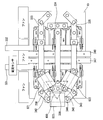
- FIG. 2 consists of FIGS. 2A to 2D.
- 2A is a plan view showing a state in the middle of assembly in which six bidirectional switching elements 31 (one of which is also referred to as an IGBT module) are mounted on the upper surface of the heat sink 10, and FIG. 2B shows each bidirectional switching.
- FIG. 2C is a plan view showing a state where the bus bar for connecting the terminal of the element 31 is mounted, and FIG. 2C shows three diodes constituting the snubber circuit 32 and three of the filter capacitors 82 of the filter circuit 8 on the left side.
- FIG. 2D is a side view of a plan view showing a state where the filter capacitor is mounted and during assembly. Since the components constituting the power conversion device 3 of this example overlap each other in plan view, the main part will be shown in a separate figure in the following description.
- the bidirectional switching element 31 of the present example is a midpoint terminal of two IGBTs paired with the input side terminal and the output side terminal of the bidirectional switching element 31 on the upper surface of the module package. And are provided.
- the leftmost terminals of the three bidirectional switching elements 311, 313, and 315 are input terminals, the rightmost terminals are output terminals, and the middle terminals are intermediate points. Terminal.
- the rightmost terminals of the three bidirectional switching elements 312, 314 and 316 on the right side are input terminals, the leftmost terminal is an output terminal, and the central terminal is Intermediate point terminal.
- the gate terminal of the bidirectional switching element 31 is provided in another part of the module package, the illustration thereof is omitted.
- the six bidirectional switching elements 311 to 316 are fixed to the upper surface of the heat sink 10 by fixing means such as bolts.
- These six bidirectional switching elements 311 to 316 are composed of a pair of bidirectional switching elements 311 and 312, bidirectional switching elements 313 and 314, and bidirectional switching elements 315 and 316, respectively.
- bidirectional switching element Reference numerals 313 and 314 and bidirectional switching elements 315 and 316 are arranged on the left and right of the center line CL, respectively.
- this arrangement is also referred to as “arranged in parallel to the center line CL or the output lines P and N connecting the output terminals”.
- the arrangement is different from the arrangement shown in FIG.
- the paired bidirectional switching elements are a pair of bidirectional switching elements connected to the same phase R, S, T of the input line.
- the bidirectional switching elements 311 and 312, the bidirectional switching elements 313 and 314, and the bidirectional switching elements 315 and 316 that are paired are arranged side by side on the left and right sides of the center line CL, so that the output lines P and N
- the layout allows the (bus bars 331 and 332) to be drawn out in one direction with the shortest distance. If the wiring length to which the high-frequency AC power is output is long, it is easily affected by the L component. Therefore, according to the arrangement of this example, the influence of the L component can be suppressed. This is an advantageous effect compared with the arrangement according to another example of FIG. That is, the output lines P and N are almost in a straight line until reaching the transformer 4.
- the rightmost terminals of the bidirectional switching elements 311, 313, and 315 on the left side of the center line CL are all output terminals, and the leftmost terminals are all input terminals.
- the leftmost terminals of the bidirectional switching elements 312, 314, and 316 on the right side of the center line CL are all output terminals, and the rightmost terminals are all input terminals.
- One input line R, S, T branched from the input line of the three-phase AC power supply 2 is connected to the center line CL at the leftmost input terminal of the bidirectional switching elements 311, 313, 315 on the left side of the center line CL.
- the other input lines R, S, branched from the input lines of the three-phase AC power source 2 are connected to the right end input terminals of the bidirectional switching elements 312, 314, 316 on the right side of the center line CL.
- T is connected toward the center line CL. That is, the R phase is connected to the input terminals of the bidirectional switching elements 311 and 312, the S phase is connected to the input terminals of the bidirectional switching elements 313 and 314, and the T phase is connected to the input terminals of the bidirectional switching elements 315 and 316. ing.
- the input lines R, S, T from the three-phase AC power source 2 to the power converter 3 are configured to branch between the filter reactor 81 and the filter capacitors 82L, 82R.
- the filter reactor 81 may be provided in each of the branched input lines R, S, and T.
- one bus bar 331 constituting the output line P of the power converter 3 is connected to the right end output terminal of the bidirectional switching elements 311, 313, 315 on the left side of the center line CL, while the center line
- One bus bar 332 constituting the output line N of the power converter 3 is connected to the output terminals at the left ends of the bidirectional switching elements 312, 314, 316 on the right side of the CL.
- the front ends of these bus bars 331 and 332 are connected to the transformer 4.
- the following bus bars including these bus bars 331 and 332 are made of a conductive material such as copper.
- the input terminals of the bidirectional switching elements 311 and 312 forming a pair arranged on the left and right of the center line CL are connected by a bus bar 333, and the input terminals of the bidirectional switching elements 313 and 314 are connected by a bus bar 334.
- the input terminals of the switching elements 315 and 316 are connected by a bus bar 335.
- the wiring corresponding to the bus bar is indicated by the same reference numeral. Note that the bus bars 333 to 335 are not essential for the function of the power conversion device 3 and may be omitted.
- bus bars 333 to 335 intersect the bus bars 331 and 332 constituting the output lines P and N in a plan view, but the bus bars 333 to 335 for connecting the input terminals as shown in the side view of FIG. By being set at a position higher than the bus bars 331 and 332 of the output lines P and N, the two are crossed so that they do not interfere with each other.
- 82L and 82R can be shared with each other. That is, a filter capacitor 821 is provided between the left R phase and the S phase in FIG. 3, and a filter capacitor 824 is provided between the right R phase and the S phase.
- the input terminals of the bidirectional switching elements 311 and 312 are connected by a bus bar 333. Therefore, since the two filter capacitors 821 and 824 cooperate to filter the R-phase noise of the three-phase AC power supply 2, one filter capacitor can be reduced in size, resulting in a smaller filter capacitor. It will be possible. The same can be said for the S phase and the T phase.
- the filter circuit 8 includes six filter capacitors 821 to 826, and three filter circuits 8 are arranged on each of the left and right input lines of the center line CL as shown in FIG.
- the left filter capacitor 821 is provided between the R phase and the S phase corresponding to the input terminal of the bidirectional switching element 311.
- the left filter capacitor 822 is provided between the S phase and the T phase corresponding to the input terminal of the bidirectional switching element 313, and the left filter capacitor 823 corresponds to the input terminal of the bidirectional switching element 315.
- the T phase and the R phase Provided between the T phase and the R phase.
- the right filter capacitor 824 is provided between the R phase and the S phase corresponding to the input terminal of the bidirectional switching element 312, and the right filter capacitor 825 corresponds to the input terminal of the bidirectional switching element 314.
- the right filter capacitor 826 is provided between the S phase and the T phase, and the right filter capacitor 826 is provided between the T phase and the R phase corresponding to the input terminal of the bidirectional switching element 316.
- filter capacitors 821 to 826 correspond to the six bidirectional switching elements 311 to 316 arranged three on each side of the center line CL. By disposing them, it is possible to shorten the routing distance of the connection wirings of the filter capacitors 821 to 826 and the bidirectional switching elements 311 to 316.
- three filter capacitors 821 to 826 are arranged outside the region where the six bidirectional switching elements 311 to 316 are provided with respect to the center line CL. Specifically, as shown to FIG. 2D, it fixes to the upper part of a bus-bar.
- the filter capacitors 821 to 826 outside the bidirectional switching elements 311 to 316, the distance between the left and right bidirectional switching elements 31L and 31R can be minimized, so that the distance of the heat sink 10 in the lateral direction is minimized.
- the distance can be set, and as a result, the heat sink 10 can be reduced in size as compared with the arrangement according to another example of FIG. 4A.
- the bus bar 331 is an output line P that connects the output terminals of the bidirectional switching elements 311, 313, and 315 to reach the transformer 4.
- the bus bar 333 is a bus bar that connects the input terminals of the bidirectional switching elements 311 and 312, extends to the left and right outside from both input terminals, and there are bus bars 336 and 337 for connecting the filter capacitors 823 and 826 respectively. They are connected (see FIG. 2C and FIG. 3 for the connection state with the filter capacitors 823 and 826).
- the bus bars 336 and 337 connected to both ends of the bus bar 333 are provided so as to be inclined with respect to a line connecting the input terminals of the bidirectional switching elements 311, 313 and 315, that is, a line extending in the vertical direction in FIG. ing.
- the bus bar 334 is a bus bar for connecting the input terminals of the bidirectional switching elements 313 and 314, extends from the left and right sides of both input terminals, and is connected to the filter capacitors 821, 822, 824, and 825, respectively. 338 and 339 are connected (refer to FIG. 2C and FIG. 3 for the connection state with the filter capacitors 821, 822, 824, and 825).
- the bus bars 338 and 339 connected to both ends of the bus bar 334 extend along lines connecting the input terminals of the bidirectional switching elements 311, 313 and 315, that is, lines extending vertically in the upper left diagram of FIG. 2. To do.
- the bus bar 335 is a bus bar that connects the input terminals of the bidirectional switching elements 315 and 316, extends to the left and right outside from both input terminals, and bus bars 340 and 341 for connecting the filter capacitors 823 and 826, respectively. They are connected (see FIG. 2C and FIG. 3 for the connection state with the filter capacitors 823 and 826).
- the bus bars 340 and 341 connected to both ends of the bus bar 335 are provided to be inclined with respect to a line connecting the input terminals of the bidirectional switching elements 311, 313 and 315, that is, a line extending in the vertical direction in FIG. ing.
- these bus bars 333, 334, and 335 are connected to the input terminals of the bidirectional switching elements 311 to 316 via several bus bars 345 and 346, and constitute the output lines P and N. , 332 and higher.
- the bus bars 333 to 335 and the bus bars 331 and 332 intersect with each other with a predetermined gap in the height direction without interference.
- the filter capacitors 821, 822, and 823 are triangles that are arranged on the outer side with respect to the center line CL and whose one vertex faces outward as shown by the broken line in FIG. 2C (an isosceles triangle or equilateral triangle is more preferable). Are arranged such that the centers of the filter capacitors 821, 822, and 823 are located at the respective vertices. By arranging the three filter capacitors 821, 822, and 823 at each vertex of the triangle, the wiring length between the capacitors can be set to the shortest distance, and the power converter 3 can be downsized. Tuning between capacitors can be achieved.
- the balance of the wiring connected to each capacitor is improved as compared with the arrangement in which one vertex faces in the inward direction, and the distance to each bus bar 333, 334, 335. Is also shortened.
- the bus bars 336 and 340 and the bus bars 337 and 341 connected to the filter capacitors 823 and 826 are inclined so as to be close to each other, the distance between the filter capacitors 823 and 826 and the bus bars 333 and 335 is further shortened. This can contribute to uniform wiring length between capacitors.
- bus bars 338 and 339 extending in a direction orthogonal to the longitudinal direction of the bus bar 334, the bus bars 338 and 339 can be mounted regardless of the size of the filter capacitors 821, 822, 824, and 825. The degree of freedom can be increased.
- the filter capacitor 821 connected between the R phase and the S phase is mounted on the upper surface of the bus bar 342, and the filter capacitor 822 connected between the S phase and the T phase is mounted on the upper surface of the bus bar 343.
- These two bus bars 342 and 343 are connected to be inclined with respect to a line connecting the input terminals of the bidirectional switching elements 311, 313 and 315, that is, a line extending in the vertical direction in FIG. 2C.
- these two bus bars 342 and 343 are connected to the bus bars 333, 342 and 335 across the line connecting the input terminals of the bidirectional switching elements 311, 313 and 315, that is, the line extending in the vertical direction in FIG. 2C. It is connected.
- the filter capacitors 824 and 825 mounted on the right side of the center line CL are also provided symmetrically with respect to the center line CL.
- the bus bars 342 and 343 so as to be inclined with respect to the line connecting the input terminals of the bidirectional switching elements 311, 313 and 315, the wiring distance of the filter capacitor 823 connected between the R phase and the T phase is minimized. Since they can be equal, tuning can be achieved between the filter capacitors 821, 822, and 823. Further, by providing the bus bars 342 and 343 so as to straddle the line connecting the input terminals of the bidirectional switching elements 311, 313 and 315, the connection distance between the filter capacitors 821 and 822 and the bus bars 333, 334 and 335 is shortened. Therefore, the power converter 3 can be downsized.
- the filter capacitors 821 to 826 are arranged on the upper surface of the bus bar, in other words, on the opposite side of the bus bar from the bidirectional switching elements 311 to 316, so that the layout of the filter capacitors 821 to 826 can be improved. Design flexibility is increased.
- the filter capacitor 823 connected between the R phase and the T phase is mounted on the upper surface of the bus bar 344 connected between the bus bars 336 and 340.
- the bus bar 344 includes the bidirectional switching elements 311 and 313. , 315 are provided in parallel to the line connecting the input terminals.
- the snubber circuit 321 of the bidirectional switching element 311 has one terminal connected to the input terminal of the bidirectional switching element 311 and the other terminal connected to the midpoint terminal of the bidirectional switching element 311. Are connected to the output terminal of the bidirectional switching element 311.
- the three diodes are fixed and connected to brackets 351 to 356 made of conductors connected to the intermediate point terminals of the bidirectional switching elements 31L and 31R, respectively. Only the bracket 355 is shown in FIG. 2D.
- bus bars 347 and 348 are provided between the bus bars 331 and 332 constituting the output lines P and N in the same direction.
- the two bus bars 347 and 348 connected to the snubber capacitor 327 are positioned higher than the bus bars 331 and 332 constituting the output lines P and N, and the bus bars 333, 334 and 335. It is fixed at a lower position.
- the two bus bars 347 and 348 are supported by the heat sink 10 or other base (not shown).
- the bus bars 311 and 312 constituting the output lines P and N and the bus bars 347 and 348 to the snubber capacitor 327
- the bus bars 347 and 348 between the bus bars 311 and 312, the output lines P and N
- the wiring distance to the snubber capacitor 327 can be shortened.
- the bus bars 347 and 348 at positions higher than the bus bars 311 and 312, the distances from the diodes of the respective snubber circuits 321 to 326 can be shortened.
- filter capacitors 821 to 826 are arranged three to the left and right of the center line CL with respect to the six bidirectional switching elements 311 to 316 arranged three to the left and right of the center line CL, respectively. Since they are arranged correspondingly, it is possible to shorten the distance between the connection wirings of the filter capacitors 821 to 826 and the bidirectional switching elements 311 to 316.
- the bidirectional switching elements 311 and 312, the bidirectional switching elements 313 and 314, and the bidirectional switching elements 315 and 316 are arranged side by side on the left and right sides of the center line CL.
- the layout is such that the lines P and N (bus bars 331 and 332) can be drawn short in one direction. Therefore, if the wiring length from which the high-frequency AC power is output is long, it is easily affected by the L component, but according to the arrangement of this example, the influence of the L component can be suppressed.
- three filter capacitors 821 to 826 are arranged on the left and right sides of the center line CL rather than the region where the six bidirectional switching elements 311 to 316 are provided.
- the distance between the left and right bidirectional switching elements 31L and 31R can be minimized. Therefore, the distance in the left-right direction of the heat sink 10 can be set to the shortest distance, and as a result, the heat sink 10 can be reduced in size.
- the input terminals of the bidirectional switching elements 311 and 312, the bidirectional switching elements 313 and 314, and the bidirectional switching elements 325 and 316 that are arranged on the left and right of the center line CL are respectively connected to the bus bar 333. Since they are connected at 334 and 335, the filter capacitors 82L and 82R provided between the phases can be shared with each other. Therefore, the capacity of one filter capacitor can be reduced, and as a result, the filter capacitor can be reduced in size.
- connection directions of the left and right input lines R, S, and T are all directed toward the center line CL with respect to the input terminals of the bidirectional switching elements 31L and 31R.
- the distance in the direction can be shortened.
- the filter capacitors 821 to 826 are disposed on the upper surface of the bus bar, in other words, on the opposite side of the bus bar from the bidirectional switching elements 311 to 316.
- the degree of freedom in designing the layout of 826 increases.
- bus bars 347 and 348 are arranged between the bus bars 311 and 312. Both the wiring distances to the lines P and N and the snubber capacitor 327 can be shortened.
- the bus bars 347 and 348 are set at positions higher than the bus bars 311 and 312, so that the distance from the diode of each of the snubber circuits 321 to 326 can be shortened.
- the wiring length between the capacitors can be set to the shortest distance, and the power converter 3 can be downsized. It is also possible to tune between capacitors.
- the bus bars 342 and 343 are provided to be inclined with respect to the line connecting the input terminals of the bidirectional switching elements 311, 313 and 315, so that the filter capacitors connected between the R phase and the T phase It is possible to make it equal to the wiring distance of 823 as much as possible. Therefore, tuning can be achieved between the filter capacitors 821, 822, and 823.
- the bus bars 342 and 343 are provided so as to straddle the line connecting the input terminals of the bidirectional switching elements 311, 313 and 315, so that the connection between the filter capacitors 821 and 822 and the bus bars 333, 334 and 335 is performed.
- a distance can be shortened and size reduction of the power converter device 3 can be achieved.
- three filter capacitors 82L and 82R on each of the left and right sides are provided outside the bidirectional switching elements 311 313 315 and 312 314 316 with respect to the center line CL.
- FIGS. 4A and 4B it can be arranged between the bidirectional switching elements 311, 313, 315 and 312, 314, 316 arranged on the left and right with respect to the center line CL.
- bidirectional switching elements 311 to 316 are arranged on the left side with respect to the center line CL, and the bidirectional switching elements 311 313, and 315 are arranged on the right side.
- the bidirectional switching elements 311, 314, 316 are arranged along the center line CL as shown in FIG. 5, but the bidirectional switching elements 311, 313, 315 and the bidirectional switching elements 312, 314, 316 are arranged. May be.
- bidirectional switching elements 311 to 316 are arranged on the left side with respect to the center line CL, and the bidirectional switching elements 311 313, and 315 are arranged on the right side.
- the input terminals and the output terminals of the bidirectional switching elements are arranged symmetrically with respect to the center line CL.
- Bidirectional switching elements 311, 313, and 315 may be disposed on the left side
- bidirectional switching elements 312, 314, and 316 may be disposed on the right side
- the input terminals and output terminals of the bidirectional switching elements may be the same.
- the two systems of input lines R, S, and T are connected to the input terminals of the bidirectional switching elements in the same direction (left to right in the illustrated example).
- filter capacitors 821 to 826 are provided between the phases so as to correspond to each of the six bidirectional switching elements 311 to 316. As shown in FIG. 7, filter capacitors 821 to 826 may be provided between the respective phases so as to correspond to each of the six bidirectional switching elements 311 to 316 (two in the illustrated example).
- the filter capacitor may be arranged at the center of the power conversion device 3 as shown in FIG. 8 or outside the power conversion device 3 as shown in FIG. As shown in FIG. 8, when the power converter 3 is arranged at the center, an empty space can be used, so that the size of the power converter 3 can be suppressed as much as possible.
- the bidirectional switching elements 311, 313 and 315 correspond to the first switching element in the claims of the present invention
- the bidirectional switching elements 312, 314 and 316 correspond to the second switching element in the claims of the present invention
- the power conversion device 3 corresponds to the conversion circuit in the claims of the present invention
- the filter capacitors 821 to 826, 831 to 836 correspond to the capacitors in the claims of the present invention
- the bus bars 331 and 332 correspond to the claims of the present invention. It corresponds to the output line in the term.
Abstract
Description
最初に本発明の一実施の形態を適用した電力変換システムの概要について図1を参照して説明する。本例の電力変換システム1は、三相交流電源2から供給される三相交流電力を本発明の一実施の形態に係る電力変換装置3により単相交流電力に直接変換し、これをトランス4により適宜の電圧に昇圧又は降圧させたのち、整流器5により直流電力に変換して二次電池6を充電するシステムである。なお、7は平滑回路である。 << Outline of
First, an outline of a power conversion system to which an embodiment of the present invention is applied will be described with reference to FIG. The
次に、図1の電力変換装置3を構成する部品の空間的な配置構成について、図2~図6を参照して説明する。なお、図1と同じ部品には同一の符号を付すことで互いの対応関係を示すものとする。 << Part arrangement of
Next, the spatial arrangement of the components that constitute the
1)本例では、中心線CLの左右に3つずつ配置された6つの双方向スイッチング素子311~316に対して、中心線CLの左右に3個ずつ6個のフィルタコンデンサ821~826をそれぞれ対応して配置したので、フィルタコンデンサ821~826と双方向スイッチング素子311~316とのそれぞれの接続配線の取り廻し距離を短くすることができる。 According to the above embodiment, it has the following advantages.
1) In this example, six
本発明は、上述した実施の形態以外にも適宜改変することができる。以下に本発明の変形例を説明するが、本発明は上述した実施の形態及び以下の実施の形態にのみ限定される趣旨ではない。なお、上述した実施の形態と共通する部材には同一の符号を付し、適宜その説明を省略する。 << Other Embodiments >>
The present invention can be modified as appropriate in addition to the embodiment described above. Although the modification of this invention is demonstrated below, this invention is not the meaning limited only to embodiment mentioned below and the following embodiment. In addition, the same code | symbol is attached | subjected to the member which is common in embodiment mentioned above, and the description is abbreviate | omitted suitably.
Claims (7)
- 多相交流電力を交流電力に直接変換する電力変換装置であって、
前記多相交流電力の各相に接続されて双方向への通電を切り換え可能にする複数の第1スイッチング素子と、前記多相交流電力の各相に接続されて双方向への通電を切り換え可能にする複数の第2スイッチング素子と、を有する変換回路と、
前記変換回路に接続された複数のコンデンサと、を備え、
前記第1スイッチング素子及び前記第2スイッチング素子のそれぞれに対応する前記多相交流電力の各相の間に、少なくとも一つの前記コンデンサが設けられ、
空間的配置として、
前記複数の第1スイッチング素子のそれぞれの端子および前記複数の第2スイッチング素子のそれぞれの端子は、それぞれ一列に配列され、
前記複数のコンデンサのうちの一部のコンデンサは、前記端子の配列方向に対して傾斜して設けられている電力変換装置。 A power converter that directly converts polyphase AC power to AC power,
A plurality of first switching elements that are connected to each phase of the multiphase AC power and capable of switching energization in both directions, and are connected to each phase of the polyphase AC power and switchable in both directions. A plurality of second switching elements, and a conversion circuit comprising:
A plurality of capacitors connected to the conversion circuit,
At least one capacitor is provided between each phase of the multiphase AC power corresponding to each of the first switching element and the second switching element,
As a spatial arrangement,
Each terminal of the plurality of first switching elements and each terminal of the plurality of second switching elements are arranged in a line, respectively.
A part of the plurality of capacitors is a power conversion device provided to be inclined with respect to an arrangement direction of the terminals. - 前記一部のコンデンサの両端の接続端子は、前記一列に配列された複数の端子を結ぶ線を跨いで配置されている請求項1に記載の電力変換装置。 The power conversion device according to claim 1, wherein the connection terminals at both ends of the partial capacitor are arranged across a line connecting the plurality of terminals arranged in a row.
- 前記複数のコンデンサのうちの他のコンデンサは、前記端子の配列方向に平行に配置されている請求項1に記載の電力変換装置。 2. The power conversion device according to claim 1, wherein the other capacitor among the plurality of capacitors is disposed in parallel with the arrangement direction of the terminals.
- 前記他のコンデンサと前記相とを接続する配線は、前記端子の配列方向に対して傾斜して設けられている請求項3に記載の電力変換装置。 4. The power conversion device according to claim 3, wherein the wiring connecting the other capacitor and the phase is provided inclined with respect to the arrangement direction of the terminals.
- 前記端子の配列方向に垂直方向に延在し、ある相に対応する第1スイッチング素子及び第2スイッチング素子の少なくとも一方が接続された第1バスバーと、
前記第1バスバーの一端部から前記配列方向に延在して前記一部のコンデンサの一方の接続端子に接続された第2バスバーと、を備える請求項1に記載の電力変換装置。 A first bus bar extending in a direction perpendicular to the arrangement direction of the terminals and connected to at least one of a first switching element and a second switching element corresponding to a certain phase;
2. A power converter according to claim 1, further comprising: a second bus bar extending from one end of the first bus bar in the arrangement direction and connected to one connection terminal of the partial capacitor. - 各相に対応する複数の直線状のバスバーが互いに平行に配置され、前記一部のコンデンサは、これらのバスバーに対して傾斜して配置されている請求項1に記載の電力変換装置。 The power converter according to claim 1, wherein a plurality of linear bus bars corresponding to each phase are arranged in parallel to each other, and the partial capacitors are arranged to be inclined with respect to these bus bars.
- 前記バスバーは、同じ相に対応する前記第1スイッチング素子の入力端子と前記第2スイッチング素子の入力端子とを互いに接続している請求項6に記載の電力変換装置。 The power converter according to claim 6, wherein the bus bar connects the input terminal of the first switching element and the input terminal of the second switching element corresponding to the same phase to each other.
Priority Applications (6)
| Application Number | Priority Date | Filing Date | Title |
|---|---|---|---|
| CN201280025374.8A CN103650317B (en) | 2011-05-31 | 2012-05-07 | Power-converting device |
| US14/122,268 US9490721B2 (en) | 2011-05-31 | 2012-05-07 | Power conversion device |
| BR112013030560-6A BR112013030560B1 (en) | 2011-05-31 | 2012-05-07 | power converter that directly converts polyphase ac current to ac current |
| MX2013013987A MX2013013987A (en) | 2011-05-31 | 2012-05-07 | Power conversion device. |
| EP12792428.0A EP2717452B1 (en) | 2011-05-31 | 2012-05-07 | Power conversion device |
| RU2013158883/07A RU2557561C1 (en) | 2011-05-31 | 2012-05-07 | Energy conversion device |
Applications Claiming Priority (2)
| Application Number | Priority Date | Filing Date | Title |
|---|---|---|---|
| JP2011-122842 | 2011-05-31 | ||
| JP2011122842A JP5377574B2 (en) | 2011-05-31 | 2011-05-31 | Power converter |
Publications (1)
| Publication Number | Publication Date |
|---|---|
| WO2012165103A1 true WO2012165103A1 (en) | 2012-12-06 |
Family
ID=47258967
Family Applications (1)
| Application Number | Title | Priority Date | Filing Date |
|---|---|---|---|
| PCT/JP2012/061658 WO2012165103A1 (en) | 2011-05-31 | 2012-05-07 | Power conversion device |
Country Status (9)
| Country | Link |
|---|---|
| US (1) | US9490721B2 (en) |
| EP (1) | EP2717452B1 (en) |
| JP (1) | JP5377574B2 (en) |
| CN (1) | CN103650317B (en) |
| BR (1) | BR112013030560B1 (en) |
| MX (1) | MX2013013987A (en) |
| MY (1) | MY158683A (en) |
| RU (1) | RU2557561C1 (en) |
| WO (1) | WO2012165103A1 (en) |
Families Citing this family (7)
| Publication number | Priority date | Publication date | Assignee | Title |
|---|---|---|---|---|
| JP5437312B2 (en) | 2011-05-31 | 2014-03-12 | 日産自動車株式会社 | Power converter |
| JP5377575B2 (en) * | 2011-05-31 | 2013-12-25 | 日産自動車株式会社 | Power converter |
| JP5476510B2 (en) * | 2011-10-07 | 2014-04-23 | 日産自動車株式会社 | Power converter |
| EP2765700B1 (en) * | 2011-10-07 | 2017-04-26 | Nissan Motor Co., Ltd | Power converter |
| DE112016003507T5 (en) * | 2015-08-28 | 2018-04-19 | Murata Manufacturing Co., Ltd. | DC converter |
| RU176542U1 (en) * | 2017-02-07 | 2018-01-23 | Открытое акционерное общество "Электровыпрямитель" | Device for generating control pulses of a diode-thyristor bridge |
| JP6488421B1 (en) * | 2018-09-12 | 2019-03-20 | 高周波熱錬株式会社 | Snubber circuit, power semiconductor module, and induction heating power supply device |
Citations (8)
| Publication number | Priority date | Publication date | Assignee | Title |
|---|---|---|---|---|
| JPH01231662A (en) * | 1988-03-09 | 1989-09-14 | Origin Electric Co Ltd | Dc power supply |
| JPH03145929A (en) * | 1989-10-31 | 1991-06-21 | Mitsubishi Electric Corp | Inverter apparatus |
| JPH06165524A (en) * | 1992-11-25 | 1994-06-10 | Hitachi Ltd | Inverter apparatus |
| JP2002252535A (en) * | 2001-02-23 | 2002-09-06 | Densei Lambda Kk | Three-phase noise filter |
| JP2005065357A (en) * | 2003-08-12 | 2005-03-10 | Hitachi Ltd | Matrix converter system |
| JP2005237138A (en) * | 2004-02-20 | 2005-09-02 | Hitachi Ltd | Power converter |
| JP2006333590A (en) * | 2005-05-25 | 2006-12-07 | Fuji Electric Fa Components & Systems Co Ltd | Ac-ac power converter |
| JP2010263702A (en) * | 2009-05-07 | 2010-11-18 | Denki Kogyo Co Ltd | Three-phase/single-phase direct power converter circuit |
Family Cites Families (40)
| Publication number | Priority date | Publication date | Assignee | Title |
|---|---|---|---|---|
| WO1980001742A1 (en) * | 1979-02-08 | 1980-08-21 | Tatsuta Densen Kk | Interphase unbalance detector for ac load circuit |
| US4468725A (en) * | 1982-06-18 | 1984-08-28 | Texas Instruments Incorporated | Direct AC converter for converting a balanced AC polyphase input to an output voltage |
| US4833584A (en) * | 1987-10-16 | 1989-05-23 | Wisconsin Alumni Research Foundation | Quasi-resonant current mode static power conversion method and apparatus |
| JPH0628292B2 (en) | 1988-11-11 | 1994-04-13 | 富士電機株式会社 | Reverse blocking transistor module |
| US5010471A (en) * | 1989-06-26 | 1991-04-23 | Robert F. Frijouf | Three-phase AC-to-AC series resonant power converter with reduced number of switches |
| GB2242580B (en) | 1990-03-30 | 1994-06-15 | Mitsubishi Electric Corp | Inverter unit with improved bus-plate configuration |
| US5287260A (en) * | 1991-10-21 | 1994-02-15 | Kabushiki Kaisha Toshiba | GTO rectifier and inverter |
| JP3195105B2 (en) * | 1993-02-26 | 2001-08-06 | 株式会社東芝 | DC power supply circuit for multi-phase input |
| JPH06261556A (en) | 1993-03-04 | 1994-09-16 | Toshiba Corp | Semiconductor switch apparatus |
| US5517063A (en) | 1994-06-10 | 1996-05-14 | Westinghouse Electric Corp. | Three phase power bridge assembly |
| SE9500761D0 (en) | 1995-03-02 | 1995-03-02 | Abb Research Ltd | Protection circuit for series-connected power semiconductors |
| US6266258B1 (en) | 1995-09-29 | 2001-07-24 | Rockwell Technologies, Llc | Power substrate element topology |
| FI110370B (en) | 1998-07-31 | 2002-12-31 | Lexel Finland Ab Oy | Arrangement to eliminate radio interference from electronic power regulator |
| JP2001045772A (en) * | 1999-08-03 | 2001-02-16 | Yaskawa Electric Corp | 3-level inverter or pwn cycloconverter |
| DE10014641C2 (en) | 2000-03-24 | 2002-03-07 | Siemens Ag | Circuit arrangement with a bidirectional circuit breaker in common collector mode and with an active overvoltage protection device |
| DE10037970A1 (en) | 2000-08-03 | 2002-03-07 | Siemens Ag | Low induction busbar for a matrix converter |
| JP3793407B2 (en) | 2000-09-19 | 2006-07-05 | 株式会社日立製作所 | Power converter |
| JP4293000B2 (en) | 2004-01-29 | 2009-07-08 | 株式会社日立製作所 | Power converter |
| US7626840B2 (en) * | 2004-09-29 | 2009-12-01 | Kabushiki Kaisha Yaskawa Denki | Parallel multiplex matrix converter |
| JP4581777B2 (en) | 2005-03-24 | 2010-11-17 | トヨタ自動車株式会社 | Power module |
| US7969755B2 (en) * | 2005-09-09 | 2011-06-28 | Siemens Aktiengesellschaft | Apparatus for electrical power transmission |
| KR20080094917A (en) | 2006-02-17 | 2008-10-27 | 가부시키가이샤 야스카와덴키 | Power converter provided with bus bar |
| JP4793096B2 (en) * | 2006-05-24 | 2011-10-12 | 株式会社明電舎 | High voltage AC direct power converter |
| CN101523710B (en) * | 2006-06-06 | 2014-03-05 | 威廉·亚历山大 | Universal power converter |
| US8008805B2 (en) | 2006-12-07 | 2011-08-30 | Nissan Motor Co., Ltd. | Power conversion apparatus and motor drive system |
| JP4720756B2 (en) | 2007-02-22 | 2011-07-13 | トヨタ自動車株式会社 | Semiconductor power conversion device and manufacturing method thereof |
| US7573732B2 (en) | 2007-05-25 | 2009-08-11 | General Electric Company | Protective circuit and method for multi-level converter |
| US20090052134A1 (en) | 2007-08-22 | 2009-02-26 | Casteel Jordan B | Liquid-cooled grounded heatsink for diode rectifier system |
| JP4640423B2 (en) | 2008-03-04 | 2011-03-02 | 株式会社豊田自動織機 | Power converter |
| EP2099119B1 (en) | 2008-03-04 | 2014-11-19 | Kabushiki Kaisha Toyota Jidoshokki | Power converter apparatus |
| CN101540580B (en) * | 2008-03-18 | 2012-03-14 | 新能动力(北京)电气科技有限公司 | Electric energy feedback device |
| JP5387859B2 (en) * | 2008-05-30 | 2014-01-15 | 株式会社安川電機 | Matrix converter control device and output voltage generation method thereof |
| EP2296156A1 (en) | 2009-08-13 | 2011-03-16 | ABB Research Ltd | Composite capacitance and use thereof |
| US8411474B2 (en) | 2010-04-30 | 2013-04-02 | General Electric Company | System and method for protection of a multilevel converter |
| JP5590448B2 (en) | 2010-07-20 | 2014-09-17 | 株式会社安川電機 | Matrix converter |
| JP2012054449A (en) | 2010-09-02 | 2012-03-15 | Aisin Aw Co Ltd | Electric connection device |
| EP2512023A3 (en) | 2011-04-14 | 2017-06-28 | General Electric Technology GmbH | Power converter arrangement and method for operating a power converter arrangement |
| JP5476510B2 (en) | 2011-10-07 | 2014-04-23 | 日産自動車株式会社 | Power converter |
| EP2765700B1 (en) | 2011-10-07 | 2017-04-26 | Nissan Motor Co., Ltd | Power converter |
| US8830705B2 (en) * | 2011-12-19 | 2014-09-09 | Zbb Energy Corporation | System and method for low speed control of polyphase AC machine |
-
2011
- 2011-05-31 JP JP2011122842A patent/JP5377574B2/en active Active
-
2012
- 2012-05-07 RU RU2013158883/07A patent/RU2557561C1/en active
- 2012-05-07 EP EP12792428.0A patent/EP2717452B1/en active Active
- 2012-05-07 BR BR112013030560-6A patent/BR112013030560B1/en active IP Right Grant
- 2012-05-07 MY MYPI2013004131A patent/MY158683A/en unknown
- 2012-05-07 CN CN201280025374.8A patent/CN103650317B/en active Active
- 2012-05-07 WO PCT/JP2012/061658 patent/WO2012165103A1/en active Application Filing
- 2012-05-07 US US14/122,268 patent/US9490721B2/en active Active
- 2012-05-07 MX MX2013013987A patent/MX2013013987A/en active IP Right Grant
Patent Citations (8)
| Publication number | Priority date | Publication date | Assignee | Title |
|---|---|---|---|---|
| JPH01231662A (en) * | 1988-03-09 | 1989-09-14 | Origin Electric Co Ltd | Dc power supply |
| JPH03145929A (en) * | 1989-10-31 | 1991-06-21 | Mitsubishi Electric Corp | Inverter apparatus |
| JPH06165524A (en) * | 1992-11-25 | 1994-06-10 | Hitachi Ltd | Inverter apparatus |
| JP2002252535A (en) * | 2001-02-23 | 2002-09-06 | Densei Lambda Kk | Three-phase noise filter |
| JP2005065357A (en) * | 2003-08-12 | 2005-03-10 | Hitachi Ltd | Matrix converter system |
| JP2005237138A (en) * | 2004-02-20 | 2005-09-02 | Hitachi Ltd | Power converter |
| JP2006333590A (en) * | 2005-05-25 | 2006-12-07 | Fuji Electric Fa Components & Systems Co Ltd | Ac-ac power converter |
| JP2010263702A (en) * | 2009-05-07 | 2010-11-18 | Denki Kogyo Co Ltd | Three-phase/single-phase direct power converter circuit |
Non-Patent Citations (1)
| Title |
|---|
| See also references of EP2717452A4 * |
Also Published As
| Publication number | Publication date |
|---|---|
| RU2557561C1 (en) | 2015-07-27 |
| MX2013013987A (en) | 2014-05-27 |
| BR112013030560B1 (en) | 2020-11-03 |
| EP2717452B1 (en) | 2021-03-10 |
| EP2717452A4 (en) | 2015-11-25 |
| MY158683A (en) | 2016-10-31 |
| RU2013158883A (en) | 2015-07-10 |
| CN103650317B (en) | 2016-06-22 |
| JP5377574B2 (en) | 2013-12-25 |
| BR112013030560A2 (en) | 2016-09-27 |
| US9490721B2 (en) | 2016-11-08 |
| US20140085950A1 (en) | 2014-03-27 |
| JP2012253856A (en) | 2012-12-20 |
| CN103650317A (en) | 2014-03-19 |
| EP2717452A1 (en) | 2014-04-09 |
Similar Documents
| Publication | Publication Date | Title |
|---|---|---|
| WO2012165100A1 (en) | Power conversion device | |
| JP5437312B2 (en) | Power converter | |
| JP5437314B2 (en) | Power converter | |
| JP5377573B2 (en) | Power converter | |
| WO2012165101A1 (en) | Power conversion device | |
| JP5476510B2 (en) | Power converter | |
| WO2012165103A1 (en) | Power conversion device | |
| JP5420122B2 (en) | Power converter |
Legal Events
| Date | Code | Title | Description |
|---|---|---|---|
| 121 | Ep: the epo has been informed by wipo that ep was designated in this application |
Ref document number: 12792428 Country of ref document: EP Kind code of ref document: A1 |
|
| WWE | Wipo information: entry into national phase |
Ref document number: 14122268 Country of ref document: US |
|
| WWE | Wipo information: entry into national phase |
Ref document number: MX/A/2013/013987 Country of ref document: MX |
|
| NENP | Non-entry into the national phase |
Ref country code: DE |
|
| ENP | Entry into the national phase |
Ref document number: 2013158883 Country of ref document: RU Kind code of ref document: A |
|
| REG | Reference to national code |
Ref country code: BR Ref legal event code: B01A Ref document number: 112013030560 Country of ref document: BR |
|
| ENP | Entry into the national phase |
Ref document number: 112013030560 Country of ref document: BR Kind code of ref document: A2 Effective date: 20131127 |