BR112013030560B1 - power converter that directly converts polyphase ac current to ac current - Google Patents
power converter that directly converts polyphase ac current to ac current Download PDFInfo
- Publication number
- BR112013030560B1 BR112013030560B1 BR112013030560-6A BR112013030560A BR112013030560B1 BR 112013030560 B1 BR112013030560 B1 BR 112013030560B1 BR 112013030560 A BR112013030560 A BR 112013030560A BR 112013030560 B1 BR112013030560 B1 BR 112013030560B1
- Authority
- BR
- Brazil
- Prior art keywords
- switching elements
- capacitors
- current
- phase
- filter capacitors
- Prior art date
Links
Images


Classifications
-
- H—ELECTRICITY
- H02—GENERATION; CONVERSION OR DISTRIBUTION OF ELECTRIC POWER
- H02M—APPARATUS FOR CONVERSION BETWEEN AC AND AC, BETWEEN AC AND DC, OR BETWEEN DC AND DC, AND FOR USE WITH MAINS OR SIMILAR POWER SUPPLY SYSTEMS; CONVERSION OF DC OR AC INPUT POWER INTO SURGE OUTPUT POWER; CONTROL OR REGULATION THEREOF
- H02M5/00—Conversion of ac power input into ac power output, e.g. for change of voltage, for change of frequency, for change of number of phases
- H02M5/02—Conversion of ac power input into ac power output, e.g. for change of voltage, for change of frequency, for change of number of phases without intermediate conversion into dc
- H02M5/04—Conversion of ac power input into ac power output, e.g. for change of voltage, for change of frequency, for change of number of phases without intermediate conversion into dc by static converters
- H02M5/22—Conversion of ac power input into ac power output, e.g. for change of voltage, for change of frequency, for change of number of phases without intermediate conversion into dc by static converters using discharge tubes with control electrode or semiconductor devices with control electrode
- H02M5/275—Conversion of ac power input into ac power output, e.g. for change of voltage, for change of frequency, for change of number of phases without intermediate conversion into dc by static converters using discharge tubes with control electrode or semiconductor devices with control electrode using devices of a triode or transistor type requiring continuous application of a control signal
- H02M5/293—Conversion of ac power input into ac power output, e.g. for change of voltage, for change of frequency, for change of number of phases without intermediate conversion into dc by static converters using discharge tubes with control electrode or semiconductor devices with control electrode using devices of a triode or transistor type requiring continuous application of a control signal using semiconductor devices only
-
- H—ELECTRICITY
- H02—GENERATION; CONVERSION OR DISTRIBUTION OF ELECTRIC POWER
- H02M—APPARATUS FOR CONVERSION BETWEEN AC AND AC, BETWEEN AC AND DC, OR BETWEEN DC AND DC, AND FOR USE WITH MAINS OR SIMILAR POWER SUPPLY SYSTEMS; CONVERSION OF DC OR AC INPUT POWER INTO SURGE OUTPUT POWER; CONTROL OR REGULATION THEREOF
- H02M7/00—Conversion of ac power input into dc power output; Conversion of dc power input into ac power output
- H02M7/003—Constructional details, e.g. physical layout, assembly, wiring or busbar connections
-
- H—ELECTRICITY
- H05—ELECTRIC TECHNIQUES NOT OTHERWISE PROVIDED FOR
- H05K—PRINTED CIRCUITS; CASINGS OR CONSTRUCTIONAL DETAILS OF ELECTRIC APPARATUS; MANUFACTURE OF ASSEMBLAGES OF ELECTRICAL COMPONENTS
- H05K7/00—Constructional details common to different types of electric apparatus
- H05K7/14—Mounting supporting structure in casing or on frame or rack
- H05K7/1422—Printed circuit boards receptacles, e.g. stacked structures, electronic circuit modules or box like frames
- H05K7/1427—Housings
- H05K7/1432—Housings specially adapted for power drive units or power converters
- H05K7/14329—Housings specially adapted for power drive units or power converters specially adapted for the configuration of power bus bars
-
- H—ELECTRICITY
- H02—GENERATION; CONVERSION OR DISTRIBUTION OF ELECTRIC POWER
- H02M—APPARATUS FOR CONVERSION BETWEEN AC AND AC, BETWEEN AC AND DC, OR BETWEEN DC AND DC, AND FOR USE WITH MAINS OR SIMILAR POWER SUPPLY SYSTEMS; CONVERSION OF DC OR AC INPUT POWER INTO SURGE OUTPUT POWER; CONTROL OR REGULATION THEREOF
- H02M1/00—Details of apparatus for conversion
- H02M1/42—Circuits or arrangements for compensating for or adjusting power factor in converters or inverters
- H02M1/4208—Arrangements for improving power factor of AC input
- H02M1/4258—Arrangements for improving power factor of AC input using a single converter stage both for correction of AC input power factor and generation of a regulated and galvanically isolated DC output voltage
-
- Y—GENERAL TAGGING OF NEW TECHNOLOGICAL DEVELOPMENTS; GENERAL TAGGING OF CROSS-SECTIONAL TECHNOLOGIES SPANNING OVER SEVERAL SECTIONS OF THE IPC; TECHNICAL SUBJECTS COVERED BY FORMER USPC CROSS-REFERENCE ART COLLECTIONS [XRACs] AND DIGESTS
- Y02—TECHNOLOGIES OR APPLICATIONS FOR MITIGATION OR ADAPTATION AGAINST CLIMATE CHANGE
- Y02B—CLIMATE CHANGE MITIGATION TECHNOLOGIES RELATED TO BUILDINGS, e.g. HOUSING, HOUSE APPLIANCES OR RELATED END-USER APPLICATIONS
- Y02B70/00—Technologies for an efficient end-user side electric power management and consumption
- Y02B70/10—Technologies improving the efficiency by using switched-mode power supplies [SMPS], i.e. efficient power electronics conversion e.g. power factor correction or reduction of losses in power supplies or efficient standby modes
Abstract
DISPOSITIVO DE CONVERSÃO DE ENERGIA. É fornecido um conversor de energia 3 que converte diretamente a corrente AC polifásica em corrente AC. Um circuito conversor tem uma pluralidade de primeiros elementos de comutação 311, 313 e 315 e uma pluralidade de segundos elementos de comutação 312, 314 e 316, ambos os quais estão conectados a cada uma das fases R, S ou T, da corrente AC polifásica de modo a permitir a comutação que liga os condutores de corrente bidirecionalmente. Os condensadores 821 e 826 são fornecidos entre as fases. Os terminais de entrada dos primeiros elementos de comutação e dos segundos elementos de comutação estão dispostos de modo a formar as respectivas linhas. Alguns da pluralidade de condensadores 821 e 822 estão dispostos de forma angulada em relação à direção da disposição dos terminais. A distância de fiação entre os condensadores e os elementos de comutação pode ser reduzida.ENERGY CONVERSION DEVICE. A power converter 3 is provided which directly converts the polyphase AC current into AC current. A converter circuit has a plurality of first switching elements 311, 313 and 315 and a plurality of second switching elements 312, 314 and 316, both of which are connected to each of the R, S or T phases of the multiphase AC current so as to allow switching that connects the current conductors bidirectionally. Capacitors 821 and 826 are supplied between phases. The input terminals of the first switching elements and the second switching elements are arranged to form the respective lines. Some of the plurality of capacitors 821 and 822 are angled in relation to the direction of the terminal arrangement. The wiring distance between the capacitors and the switching elements can be reduced.
Description
[001] A presente invenção refere-se a um dispositivo de conversão de energia ou um conversor de energia, que converte diretamente a corrente CA de frequência comercial em uma energia CA arbitrária.[001] The present invention relates to an energy conversion device or an energy converter, which directly converts commercial frequency AC current into arbitrary AC power.
[002] Um conversor de matriz é conhecido como um conversor de energia que têm um pequeno número de componentes, que permite a redução do tamanho do dispositivo e converte direta e eficazmente a corrente CA em corrente CA (Documento de Patente 1 ).[002] A matrix converter is known as a power converter that has a small number of components, which allows for the reduction of the size of the device and directly and effectively converts AC current into AC current (Patent Document 1).
[003] No conversor de matriz convencional supracitado, os condensadores de filtro, que constituem um circuito de filtro, estão dispostos sobre um substrato que forma uma linha em uma direção longitudinal e estão instalados em uma caixa. No entanto, nesta disposição, o cabeamento que conecta os IGBTs (ou seja, Insulated Gate Bipolar Transístor), que são meios de comutação, aos condensadores de filtro tem um comprimento longo indesejável.[003] In the aforementioned conventional matrix converter, the filter capacitors, which constitute a filter circuit, are arranged on a substrate that forms a line in a longitudinal direction and are installed in a box. However, in this arrangement, the cabling that connects the IGBTs (ie Insulated Gate Bipolar Transistors), which are switching media, to the filter capacitors has an undesirable long length.
[004] Documento de Patente 1: Pedido de Patente Japonês ( Tokkai ) 2006 - 333590.[004] Patent Document 1: Japanese Patent Application (Tokkai) 2006 - 333590.
[005] Um objeto da presente invenção é fornecer um conversor de energia que pode encurtar a distância do cabeamento entre os condensadores de filtro e os meios de comutação.[005] An object of the present invention is to provide a power converter that can shorten the wiring distance between the filter capacitors and the switching means.
[006] Na presente invenção, alguns dos condensadores de filtro estão angulados em relação a uma direção na qual os terminais dos elementos de comutação estão dispostos.[006] In the present invention, some of the filter capacitors are angled with respect to a direction in which the terminals of the switching elements are arranged.
[007] De acordo com a presente invenção, a distância entre alguns dos con- densadores de filtro e os elementos de comutação e a distância entre os outros con-densadores de filtro e os elementos de comutação podem ser substancialmente equalizadas e, portanto, a distância do cabeamento entre os condensadores de filtro e os elementos de comutação pode ser encurtada.[007] According to the present invention, the distance between some of the filter capacitors and the switching elements and the distance between the other filter capacitors and the switching elements can be substantially equalized and, therefore, the The wiring distance between the filter capacitors and the switching elements can be shortened.
[008] A Figura 1 é um diagrama elétrico que mostra um sistema de conversão de energia no qual uma forma de realização da presente invenção é aplicada na prática.[008] Figure 1 is an electrical diagram showing an energy conversion system in which an embodiment of the present invention is applied in practice.
[009] A Figura 2A é uma vista plana de um conversor de energia da forma de realização da presente invenção em um processo de montagem.[009] Figure 2A is a plan view of an energy converter of the embodiment of the present invention in an assembly process.
[010] A Figura 2B é uma outra vista plana do conversor de energia da forma de realização da presente invenção no processo de montagem.[010] Figure 2B is another plan view of the energy converter of the embodiment of the present invention in the assembly process.
[011] A Figura 2C é ainda uma outra vista plana do conversor de energia da forma de realização da presente invenção no processo de montagem.[011] Figure 2C is yet another plan view of the energy converter of the embodiment of the present invention in the assembly process.
[012] A Figura 2D é uma vista lateral do conversor de energia da forma de realização da presente invenção no processo de montagem.[012] Figure 2D is a side view of the energy converter of the embodiment of the present invention in the assembly process.
[013] A Figura 3 apresenta as vistas plana e lateral que mostra o layout dos IGBTs e os condensadores de filtro do conversor de energia da Figura 2.[013] Figure 3 shows the plan and side views showing the layout of the IGBTs and the filter capacitors of the power converter in Figure 2.
[014] A Figura 4A é uma vista planta que descreve um outro layout dos IGBTs e os condensadores de filtro mostrados na Figura 3.[014] Figure 4A is a plan view showing another layout of the IGBTs and the filter capacitors shown in Figure 3.
[015] A Figura 4B é uma vista lateral da Figura 4A.[015] Figure 4B is a side view of Figure 4A.
[016] A Figura 5 apresenta as vistas plana e lateral que mostra ainda outro layout dos IGBTs e os condensadores de filtro mostrados na Figura 3.[016] Figure 5 shows the plan and side views that show yet another layout of the IGBTs and the filter capacitors shown in Figure 3.
[017] A Figura 6 apresenta as vistas plana e lateral que mostra outro layout de IGBTs e condensadores de filtro mostrado na Figura 3.[017] Figure 6 shows the plan and side views showing another layout of IGBTs and filter capacitors shown in Figure 3.
[018] A Figura 7 é um diagrama elétrico que mostra um sistema de conversão de energia no qual uma outra forma de realização da presente invenção é aplicada na prática.[018] Figure 7 is an electrical diagram showing an energy conversion system in which another embodiment of the present invention is applied in practice.
[019] A Figura 8 apresenta as vistas plana e lateral que mostra o layout dos IGBTs e os condensadores de filtro do conversor de energia da Figura 7.[019] Figure 8 shows the plan and side views showing the layout of the IGBTs and the filter capacitors of the power converter in Figure 7.
[020] A Figura 9 apresenta as vistas plana e lateral que mostra outro layout dos IGBTs e os condensadores de filtro do conversor de energia da Figura 7.[020] Figure 9 shows the plan and side views showing another layout of the IGBTs and the filter capacitors of the power converter in Figure 7.
[021] Em primeiro lugar, uma breve descrição de um sistema de conversão de energia ao qual uma forma de realização da presente invenção é aplicada na prática será descrita com referência à Figura 1. O sistema de conversão de energia 1 deste exemplo é um sistema no qual uma energia trifásica CA, suprida pela fonte de alimentação CA trifásica 2, é diretamente convertida em corrente CA monofásica por um conversor de energia 3, da forma de realização da presente invenção; e, depois que a tensão da corrente CA convertida é aumentada ou reduzida por um transformador 4 a um valor adequado, a corrente CA transformada é convertida por um reti- ficador 5 em uma energia DC que carrega uma bateria secundária 6. Nota-se que o número 7 indica um circuito de suavização.[021] First, a brief description of an energy conversion system to which an embodiment of the present invention is applied in practice will be described with reference to Figure 1. The energy conversion system 1 in this example is a system in which a three-phase AC power, supplied by the three-phase
[022] No sistema de conversão de energia 1 deste exemplo, as linhas de saída ( indicadas pela fase R, fase S e fase T ) pelas quais a corrente CA trifásica é fornecida pela fonte de alimentação CA trifásica 2, têm em cada fase um circuito de filtro 8 que amortece uma onda harmônica alta de forma a suprimir o ruído. O circuito de filtro 8 deste exemplo, compreende três reatores de filtro 81 conectados respectivamente às fases R, S e T, e seis condensadores de filtro 82L e 82R sendo cada um conectado entre as fases R, S e T. O layout dos condensadores de filtro 82L e 82R ( que são indicados como condensadores de filtro 821 a 836 nas Figuras 3 a 6 ) será descrita a seguir.[022] In the power conversion system 1 of this example, the output lines (indicated by the R phase, S phase and T phase) through which the three-phase AC current is supplied by the three-phase
[023] No sistema de conversão de energia 1 deste exemplo, a corrente CA trifásica é fornecida ao conversor de energia 3 através do circuito de filtro 8 e convertida na corrente CA monofásica. O conversor de energia 3 deste exemplo é equipado com seis elementos de comutação bidirecionais 31 que estão dispostos em forma de uma matriz correspondendo às fases R, S e T. A seguir, quando um elemento de comutação bidirecional for genericamente descrito, a explicação vai ser feita com o auxílio da referência numérica 31, enquanto que, como é mostrado na Figura 1, quando um elemento indicado dos seis elementos de comutação bidirecionais for descrito, a explicação vai ser feita por meio da referência numérica 311 a 316.[023] In the energy conversion system 1 of this example, the three-phase AC current is supplied to the
[024] Cada um dos elementos de comutação bidirecionais 31 deste exemplo é constituído por um módulo de IGBT no qual o IGBT ( ou seja, Insulated Gate Bipolar Transistor ), que é um elemento de comutação semi-condutor, e os diodos de refluxo são combinados e conectados através de uma conexão inversa - paralela. Nota-se que cada um dos elementos de comutação bidirecionais 31 não se limita ao que foi ilustrado. Isto é, o elemento de comutação pode ter outra construção. Por exemplo, o elemento de comutação pode ter uma construção em que dois elementos de bloqueio reverso do tipo IGBT estão conectados através de uma conexão inversa - paralela.[024] Each of the bidirectional switching elements 31 in this example consists of an IGBT module in which the IGBT (ie Insulated Gate Bipolar Transistor), which is a semi-conductive switching element, and the reflux diodes are combined and connected via a reverse - parallel connection. It is noted that each of the two-way switching elements 31 is not limited to what has been illustrated. That is, the switching element may have another construction. For example, the switching element may have a construction in which two IGBT-type reverse blocking elements are connected via a reverse - parallel connection.
[025] Cada um dos elementos de comutação bidirecionais 31 está equipado com um circuito snubber 32 para proteger o elemento de comutação bidirecional 31 de um pico de tensão inevitavelmente produzido quando o elemento de comutação bidirecional 31 é submetido à operação ON / OFF, o circuito snubber 32 inclui uma combinação de um condensador snubber e três diodos que estão dispostos nos lados de entrada e saída do elemento de comutação bidirecional 31. Em seguida, quando um circuito snubber for genericamente descrito, a explicação vai ser feita com o auxílio da referência numérica 32, enquanto que, como é mostrado na Figura 1, quando um circuito especificado dos seis circuitos snubber for descrito, a explicação vai ser feita por meio da referência numérica 321 a 326.[025] Each of the bidirectional switching elements 31 is equipped with a snubber circuit 32 to protect the bidirectional switching element 31 from a voltage peak inevitably produced when the bidirectional switching element 31 is subjected to ON / OFF operation, the circuit snubber 32 includes a combination of a snubber capacitor and three diodes that are arranged on the input and output sides of the bidirectional switching element 31. Then, when a snubber circuit is generically described, the explanation will be made with the aid of the numerical reference 32, while, as shown in Figure 1, when a specified circuit of the six snubber circuits is described, the explanation will be made by means of the
[026] O sistema de conversão de energia 1 deste exemplo está equipado com um circuito de controle do conversor de matriz 9 para efetuar o controle ON / OFF dos elementos de comutação bidirecionais 31 do conversor de energia. No circuito de controle do conversor de matriz 9, um valor de tensão fornecido pela fonte de alimentação CA trifásica 2, um valor de corrente DC que está sendo transmitido e um nível alvo da corrente solicitada são inseridos, e a seguir, com base neles, os respectivos sinais de porta dos elementos de comutação bidirecionais 31 são controlados a fim de ajustar a corrente CA monofásica dirigida ao transformador 4. Com isso, a energia da corrente contínua alvo é obtida.[026] The energy conversion system 1 of this example is equipped with a control circuit of the
[027] O transformador 4 tem a função de CA elerar ou reduzir a tensão da corrente CA monofásica que foi convertida pelo conversor de energia 3 a um valor desejado. O retificador 5 está equipado com quatro diodos retificadores que convertem a corrente CA monofásica ajustada a uma energia em corrente contínua. O circuito de suavização 7 está equipado com uma bobina e um condensador para amortecer a corrente pulsante contida na corrente contínua retificada de modo que a corrente pulsante seja amortecida a fim de mostrar uma forma muito semelhante a uma corrente contínua.[027]
[028] Pelo sistema de conversão de energia 1 com a construção acima mencionada, a corrente CA trifásica da fonte de alimentação CA trifásica 2 é diretamente convertida pelo conversor de energia 3 em uma corrente CA monofásica, e depois de ser convertida em corrente CA monofásica, sua tensão é ajustada, e a corrente CA monofásica ajustada é convertida em energia em corrente contínua. Com isso, a bateria secundária 6 é carregada. Nota-se que o referido sistema de conversão de energia 1 é um dos sistemas exemplificados no qual o conversor de energia 3 da presente invenção é aplicado na prática e a presente invenção não está limitada em ser aplicada apenas no referido sistema de conversão de energia 1. Isto é, quando pelo menos uma de uma energia elétrica que será convertida e uma energia elétrica que foi convertida for uma corrente CA polifásica, a presente invenção é aplicável a outros sistemas de conversão de energia.[028] By the power conversion system 1 with the aforementioned construction, the three-phase AC current from the three-phase
[029] Então, a disposição espacial das peças que constituem o conversor de energia 3 da Figura 1 será descrita com referência às Figuras 2 a 6. Nota-se que as peças idênticas às mostradas na Figura 1 são indicadas pela mesma referência numérica por mostrarem relação mútua entre elas.[029] Then, the spatial arrangement of the parts that make up the
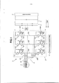
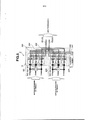
[030] A Figura 2 inclui as Figuras 2A a 2D. A Figura 2A é uma vista plana de um processo de montagem que mostra seis elementos de comutação bidirecionais 31 ( sendo cada um denominado como módulo IGBT) montado numa superfície superior de um dissipador de calor 10. A Figura 2B é uma vista plana que mostra o processo de montagem, além dos elementos de comutação bidirecionais, os barra- mentos que são fornecidos para conectar os terminais dos elementos de comutação bidirecionais 31. A Figura 2C é uma vista plana de um processo de montagem de três diodos que são partes do circuito snubber 32 e os condensadores de filtro 82 do circuito de filtro 8, mostrando no lado esquerdo três condensadores de filtro montados. A Figura 2D é uma vista lateral do dispositivo acima mencionado. Uma vez que as partes que constituem o conversor de energia 3 da presente invenção estão mutuamente sobrepostas quando vistas num plano, a explicação das porções essenciais será feita com o auxílio dos outros desenhos.[030] Figure 2 includes Figures 2A to 2D. Figure 2A is a plan view of an assembly process showing six bi-directional switching elements 31 (each called an IGBT module) mounted on an upper surface of a
[031] Tal como é mostrado nas Figuras 2 e 3, cada elemento de comutação bidirecional 31 do presente exemplo é fornecido em uma superfície superior de um corpo do módulo com os terminais de entrada e de saída e um terminal intermediário que é um dos dois terminais intermediários fornecidos respectivamente pelos dois pares de IGBTs. Dos seis elementos de comutação bidirecionais 311 a 316 mostrados na Figura 3, os três elementos de comutação bidirecionais do lado esquerdo 311, 313 e 315 têm, em cada um, o terminal de entrada na extremidade esquerda, o terminal de saída na extremidade direita e o terminal intermediário no meio. Além disso, dentre os seis elementos de comutação bidirecionais 311 a 316 mostrados na Figura 3, o lado direito dos três elementos de comutação bidirecionais 312, 314 e 316 têm, em cada um, o terminal de entrada na extremidade direita, o terminal de saída na extremidade esquerda e o terminal intermediário no meio. Apesar de um terminal de porta de cada elemento de comutação bidirecional 31 ser montado em uma porção diferente do pacote do módulo, a ilustração do terminal de porta é omitida.[031] As shown in Figures 2 and 3, each bidirectional switching element 31 of the present example is provided on an upper surface of a module body with the input and output terminals and an intermediate terminal which is one of the two intermediate terminals supplied respectively by the two pairs of IGBTs. Of the six
[032] Como pode ser visto a partir das Figuras 2 e 3, os seis elementos de comutação bidirecionais 311 a 316 estão fixados à superfície superior do dissipador de calor 10 através de mecanismos de conexão, tais como parafusos ou semelhantes. Como é visto a partir de tais desenhos, os seis elementos de comutação bidirecionais 311 a 316 estão dispostos de maneira que os elementos de comutação bidirecionais pareados 311 e 312, os elementos de comutação bidirecionais pareados 313 e 314 e os elementos de comutação bidirecionais pareados 315 e 316 são colocados respectivamente nos lados esquerdo e direito em relação a uma linha central CL. Em outras palavras, os dois elementos de comutação bidirecionais 311 e 312, dois elementos de comutação bidirecionais 313 e 314 e dois elementos de comutação bidirecionais 315 e 316, que são ambos pareados em relação a uma direção na qual os três terminais ( ou seja, o terminal de entrada, terminal intermediário e terminal de saída ) de cada elemento de comutação bidirecional 31 estendem, são colocados respectivamente nos lados esquerdo e direito em relação à linha central CL. A seguir, esta disposição será reformulada como "estando disposta lado a lado em relação à linha central CL ou às linhas de saída P e N, ambas conectando os terminais de saída". Nota-se que a disposição é diferente da que é mostrada na Figura 5, que será descrita a seguir. Nota-se ainda que os elementos de comutação bidirecionais pareados significam um par de elementos de comutação bidirecionais que estão conectados à mesma fase R, S e T da linha de entrada.[032] As can be seen from Figures 2 and 3, the six
[033] Ao se colocar os elementos de comutação bidirecionais pareados 311 e 312, os elementos de comutação bidirecionais pareados 313 e 314, e os elementos de comutação bidirecionais pareados 315 e 316 nos lados esquerdo e direito, respectivamente, em relação à linha central CL, como é descrito acima, é possível prover um layout em que as linhas de saída P e N ( barramentos 331 e 332 ) são estabelecidas em uma direção com a distância mais curta. Se o comprimento da disposição do cabeamento através do qual uma corrente CA de alta frequência é transmitida for longo, a disposição é facilmente influenciada pelo componente L. Entretanto, a influência do componente L pode ser eliminada na disposição do cabeamento, de acordo com a invenção. Esta eliminação é um efeito vantajoso em compa-ração com a disposição de outro exemplo da Figura 5. Ou seja, as linhas de saída P e N mostram linhas quase em linha reta até chegar ao transformador 4.[033] When placing the paired
[034] Além disso, como mencionado anteriormente, os terminais presentes nas extremidades direitas dos elementos de comutação bidirecionais 311, 313, 315, e colocados no lado esquerdo em relação à linha central CL, são todos os terminais de saída, e os terminais presentes nas extremidades esquerdas destes são todos os terminais de entrada. Enquanto os terminais presentes nas extremidades esquerdas dos elementos de comutação bidirecionais 312, 314 e 316, e colocados do lado direito em relação à linha central CL, são todos os terminais de saída, e os terminais presentes nas extremidades direitas destes são todos os terminais de entrada.[034] Furthermore, as mentioned earlier, the terminals present at the right ends of the
[035] Aos terminais de entrada presentes nas extremidades esquerdas dos elementos de comutação bidirecionais 311, 313, 315 colocados no lado esquerdo em relação à linha central CL, estão conectadas as linhas de entrada R, S eTdeum grupo ramificado das linhas de entrada da fonte de alimentação CA trifásica 2, as linhas de entrada R, S e Tde um grupo que se estende em direção à linha central CL, e os terminais de entrada presentes nas extremidades direitas dos elementos de comutação bidirecionais 312, 314 e 416 colocados no lado direito em relação à linha central CL, esta conectadas as linhas de entrada R, S eTdo outro grupo ramificado a partir das linhas de entrada da fonte de alimentação CA trifásica 2, as linhas de entrada de R, S e T do outro grupo que se estende em direção à linha central CL. Isto é, aos terminais de entrada dos elementos de comutação bidirecionais 311 e 312, está conectada a fase R, e aos terminais de entrada dos elementos de comutação bidirecionais 313 e 314, está conectada a fase S e aos terminais de entrada dos elementos de comutação bidirecionais 315 e 316, está conectada a forma T. Ao se fazer uma direção por onde as linhas de entrada esquerda e direita R, S e T se estendem para a conexão com os terminais de entrada igual a direção para a linha central CL, uma distância do dissipador de calor 10 na direção esquerda e direita pode ser reduzida quando comparada com a de uma outra disposição mostrada na Figura 6.[035] To the input terminals present at the left ends of the
[036] Na disposição da Figura 1, as linhas de entrada R, S e T da fonte de alimentação CA trifásica 2 para o conversor de energia 3 são ramificadas em uma posição entre uma unidade de reatores de filtro 81 e uma unidade de condensadores de filtro 82L e 82R. No entanto, uma modificação pode ser empregada na qual a ramificação é feita em uma posição a montante dos reatores de filtro 81 e as linhas de entrada de R, S e T, são então ramificadas e fornecidas respectivamente com os reatores de filtro 81.[036] In the arrangement in Figure 1, the input lines R, S and T of the three-phase
[037] Aos terminais de saída presentes nas extremidades direitas dos elementos de comutação bidirecionais 311, 313, 315 colocados no lado esquerdo em relação à linha central CL, está conectado um barramento 331, que consiste na linha de saída P do conversor de energia 3, e os terminais de saída presentes nas extremidades esquerdas dos elementos de comutação bidirecionais 312, 314 e 316, colocados no lado direito em relação à linha central CL, está conectado um barramento 332, que consiste na linha de saída N do conversor de energia 3. As extremidades dianteiras destes barramentos 331 e 332 estão conectados ao transformador 4. Estes barramentos 331 e 332, e os barramentos mencionados a seguir, são construídos de um corpo condutor elétrico com boa condutividade, tal como o cobre ou simi-lares.[037] To the output terminals on the right ends of the
[038] Os terminais de entrada dos elementos de comutação bidirecionais pareados 311 e 312 colocados nos lados esquerdo e direito em relação à linha central CL estão conectados através de um barramento 333, os terminais de entrada dos elementos de comutação bidirecionais 313 e 314 estão conectados através de um barramento 334 e os terminais de entrada dos elementos de comutação bidirecionais 315 e 316 estão conectados através de um barramento 335. Em um circuito equivalente da Figura 1, as fiações correspondentes a tais barramentos são indicadas pela mesma referência numérica. Tendo em conta a função do conversor de energia 3, estes barramentos 333 a 335 não são essenciais. Assim, estes barramentos podem ser omitidos.[038] The input terminals of the paired
[039] Quando visualizados em uma vista plana, estes barramentos 333 a 335 são dispostos de modo a atravessar os barramentos 331 e 332 que constituem as linhas de saída P e N. Contudo, tal como é visto a partir da vista lateral da Figura 3, os barramentos 333 a 335 que conectam os terminais de entrada opostos estão dispostos em uma posição acima dos barramentos 331 e 332 das linhas de saída P e N, e, assim, é realizado o chamado cruzamento aéreo entre eles e, deste modo, não provoca interferência mútua entre os mesmos.[039] When viewed in a flat view, these
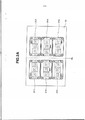
[040] Ao conectar os elementos de comutação bidirecionais pareados 311 e 312 colocados nos lados esquerdo e direito em relação à linha central CL, os elementos de comutação bidirecionais pareados 313 e 314 e os elementos de comutação bidirecionais pareados 315 e 316, os condensadores de filtro 82L e 82R, cada um deles são interpostos entre as fases que podem ser compartilhadas entre si. Isto é, entre a fase R e a fase S mostradas no lado esquerdo da Figura 1, encontra-se disposto um condensador de filtro 821; e entre a fase R e a fase S mostradas no lado direito do desenho, encontra-se disposto um condensador de filtro 824, e os terminais de entrada dos elementos de comutação bidirecionais 311 e 312, nos quais a fase R é introduzida, estão conectados através de um barramento 333. Deste modo, o ruído na fase R da fonte de alimentação CA trifásica 2 é filtrado pelos dois condensadores de filtro, 821 e 824, que cooperam entre si, e deste modo, cada condensador de filtro pode ser feito com pequena capacidade, o que resulta em cada condensador de filtro poder ser feito em tamanho pequeno. Uma vantagem semelhante é obtida a partir da cooperação de dois condensadores de filtro também na fase S e na fase T.[040] When connecting the paired two-
[041] Neste exemplo, o circuito de filtro 8 tem seis condensadores de filtro 821 a 826 e, como é visto a partir da Figura 3, as linhas de entrada colocadas nos lados esquerdo e direito em relação à linha central CL são fornecidas com três condensadores de filtro, respectivamente. O condensador de filtro do lado esquerdo 821 está disposto entre a fase R, que corresponde ao terminal de entrada do elemento de comutação bidirecional 311 e a fase S. Assim, o condensador de filtro do lado esquerdo 822 está disposto entre a fase S, que corresponde ao terminal de entrada do elemento de comutação bidirecional 313 e a fase T, e o condensador de filtro do lado esquerdo 823 está disposto entre a fase T, que corresponde ao terminal de entrada do elemento de comutação bidirecional 315 e a fase R. Enquanto que o condensador de filtro do lado direito 824 está disposto entre a fase R, que corresponde ao terminal de entrada do elemento de comutação bidirecional 312 e a fase S, o condensador de filtro do lado direito 825 está disposto entre a fase S, que corresponde ao terminal de entrada do elemento de comutação bidirecional 314 e a fase T, e o condensador de filtro do lado direito 826 está disposto entre a fase T, que corresponde ao terminal de entrada do elemento de comutação bidirecional 316 e a fase R.[041] In this example,
[042] Tal como mencionado anteriormente, através da disposição dos seis elementos de comutação bidirecionais 311 a 316 que estão dispostos de tal maneira que três elementos e os outros três elementos estejam colocados respectivamente nos lados esquerdo e direito em relação à linha central CL, os seis condensadores de filtro 821 a 826 dispostos de tal maneira que os três condensadores e os outros três condensadores estejam colocados respectivamente nos lados esquerdo e direito em relação à linha central CL, a distância do cabeamento dos cabos de conexão entre cada um dos condensadores de filtro 821 a 826 e um elemento de comutação bidirecional 311 a 316 correspondente pode ser encurtada.[042] As mentioned earlier, by arranging the six
[043] Neste exemplo, os seis condensadores de filtro 821 a 826 dos quais três condensadores de filtro e os outros três condensadores de filtro estão dispostos respectivamente nos lados esquerdo e direito, são colocados externamente a uma área onde os seis elementos de comutação bidirecionais 311 a 316 são colocados em relação à linha central CL. Especificamente, como é mostrado pela Figura 2D, os condensadores de filtro são fixados nas porções superiores dos barramentos. Ao se colocar os condensadores de filtro 821 a 826 externamente à área dos elementos de comutação bidirecionais 311 a 316, a distância na direção da esquerda para a direita entre os elementos de comutação bidirecionais 31L do lado esquerdo, e os elementos de comutação bidirecionais 31R do lado direito pode ser encurtada, assim, um, a distância na direção da esquerda para a direita do dissipador de calor 10 pode ser encurtada, o que pode levar a uma redução em tamanho do dissipador de calor 10 quando comparado com um dissipador de calor mostrado na Figura 4A, que mostra o outro exemplo.[043] In this example, the six
[044] A seguir, um estado de montagem dos condensadores de filtro 821 a 826, que são divididos em dois grupos ( cada um incluindo três condensadores de filtro ) colocados respectivamente nos lados esquerdo e direito em relação à linha central CL, será descrito com referência as vistas plana e lateral do dispositivo real da Figura 2.[044] Next, a state of assembly of
[045] Antes da sua descrição, uma estrutura de conexão dos barramentos será descrito. Como pode ser visto a partir da Figura 2B, o barramento 331 representa a linha de saída P que conecta os terminais de saída dos elementos de comutação bidirecionais 311, 313 e 315 e conduz ao transformador 4, e um barramento 332 representa a linha de saída N que conecta os terminais de saída dos elementos de comutação bidirecionais 312, 314 e 316, e conduz ao transformador 4. O barramento 333 é um barramento que conecta os terminais de entrada dos elementos de comutação bidirecionais 311 e 312, e o barramento de 333 tem porções de extensão que se prolongam para fora nas direções esquerda e direita dos respectivos terminais de entrada e as porções de extensão são conectadas respectivamente aos barramentos 336 e 337 para conectar aos condensadores de filtro 823 e 826 ( o estado de conexão destes barramentos aos condensadores de filtro 823 e 826 é entendido a partir das Figuras 2C e 3 ). Os barramentos 336 e 337 conectados respectivamente às extremidades opostas do barramento 333 estão angulados em relação a uma linha que conecta os terminais de entrada dos elementos de comutação bidirecionais 311, 313 e 315, que é uma linha que se estende na direção ascendente e descendente na Figura 2C.[045] Before its description, a connection structure for the busbars will be described. As can be seen from Figure 2B,
[046] O barramento 334 é um barramento que conecta os terminais de entrada dos elementos de comutação bidirecionais 313 e 314, e o barramento 334 tem porções de extensão que se prolongam para fora nas direções esquerda e direita dos respectivos terminais de entrada e as porções de extensão são conectadas respectivamente aos barramentos 338 e 339 para conectar os condensadores de filtro 821, 822, 824 e 825 ( o estado de conexão destes barramentos dos condensadores de filtro 821, 822, 824 e 825 é entendido a partir das Figuras 2C e 3). Os barramentos 338 e 339 estão conectados respectivamente às extremidades opostas do bar- ramento 334 que se estendem ao longo de uma linha que conecta os terminais de entrada dos elementos de comutação bidirecionais 311, 313 e 315, ou seja, uma linha que se estende na direção ascendente e descendente, na porção superior esquerda da Figura 2.[046] The 334 bus is a bus that connects the input terminals of the
[047] O barramento 335 é um barramento que conecta os terminais de entrada dos elementos de comutação bidirecionais 315 e 316, e o barramento 335 tem porções de extensão que se prolongam para fora nas direções esquerda e direita dos respectivos terminais de entrada e as porções de extensão são conectadas respectivamente aos barramentos 340 e 341 para conectar os condensadores de filtro 823 e 826 ( o estado de conexão destes barramentos dos condensadores de filtro 823 e 826 é entendido a partir das Figuras 2C e 3). Os barramentos 340 e 341 conectados respectivamente às extremidades opostas do barramento 335 estão angulados em relação a uma linha que conecta os terminais de entrada dos elementos de comutação bidirecionais 311, 313 e 315, que é uma linha que se estende no sentido ascendente e descendente na Figura 2C.[047]
[048] Como pode ser visto a partir da Figura 2D, estes barramentos 333, 334 e 335 são conectados aos terminais de entrada dos elementos de comutação bidirecionais 311 a 316 através de vários barramentos 345 e 346 e posicionados bem acima dos barramentos 331 e 332 que constituem as linhas de saída P e N. Com isso, os barramentos de 333 a 335 e os barramentos 331 e 332 são colocados de modo a constituir um cruzamento aéreo deixando um espaço pré-determinado entre os mesmos, sem provocar interferência mútua entre os mesmos.[048] As can be seen from Figure 2D, these
[049] Tal como é mostrado pelas linhas tracejadas na Figura 2C, os condensadores de filtro 821, 822 e 823 estão posicionados do lado de fora em relação à linha central CL e colocados de tal maneira que os centros dos condensadores de filtro 821, 822 e 823 estão colocados respectivamente nos vértices de um triângulo ( é preferível que seja um triângulo isosceles ou triângulo equilátero ), dos quais um vértice está dirigido para o lado de fora. Ao colocar os três condensadores de filtro 821, 822 e 823 nos vértices do triângulo, o comprimento do cabeamento entre os condensadores pode ser encurtado e, assim, o conversor de energia de 3 pode ser feito em tamanho pequeno e a sincronização entre os condensadores pode ser assegurada. Além disso, devido à disposição de um vértice dirigido para fora, o balanço do cabeamento dos condensadores é melhorado em comparação com uma disposição na qual o vértice está dirigido para dentro, e as distâncias até os respectivos barramentos 333, 334 e 335 podem ser encurtadas. Os barramentos 336 e 340 ou os barramentos 337 e 341, que estão conectados ao condensador de filtro 823 ou 826, respectivamente, formam um ângulo entre si que encurta a distância entre os mesmos. Com este disposição, as distâncias do condensador de filtro 823 ou 826 até os respectivos barramentos 333 e 335 podem ser muito reduzidas e, assim, a equalização dos comprimentos do cabeamento entre os condensadores está assegurada. Além disso, devido a disposição na qual os barramentos 338 e 339 estão dispostos de forma a estenderem em uma direção perpendicular à direção longitudinal do barramento 334, os condensadores de filtro 821, 822, 824 e 825 podem ser, na verdade, montados sem considerar os tamanhos dos mesmos e assim, o grau de liberdade na concepção dos condensadores pode ser aumentado.[049] As shown by the dashed lines in Figure 2C,
[050] O condensador de filtro 821 disposto entre a fase R e a fase S está montado sobre uma superfície superior do barramento 342 e um condensador de filtro 822 disposto entre a fase S e a fase T está montado sobre uma superfície superior do barramento 343. Estes dois barramentos 342 e 343 estão conectados enquanto estão angulados em relação a uma linha que conecta os terminais de entrada dos elementos de comutação bidirecionais 311, 313 e 315, isto é, uma linha que se estende na direção ascendente e descendente na Figura 2C. Além disso, estes dois barramentos 342 e 343 estão conectados aos barramentos 333, 342 e 335, enquanto abrangem uma linha que conecta os terminais de entrada dos elementos de comutação bidirecionais 311, 313 e 315, que é uma linha que se estende na direção ascendente e descendente na Figura 2C. Nota-se que os condensadores de filtro 824 e 825 montados no lado direito da linha central CL estão dispostos simetricamente em relação aos condensadores de filtro de 821 e 822 em relação à linha central CL.[050] The
[051] Ao se colocar os barramentos 342 e 343 de modo que estes barramentos estejam relativamente angulados à linha que conecta os terminais de entrada dos elementos de comutação bidirecionais 311, 313 e 315, a sincronização entre os condensadores de filtro 821, 822 e 823 é assegurada porque a distância do cabeamento entre os condensadores de filtro pode ser finamente equalizada com a distância do cabeamento do condensador de filtro 823 disposta entre a fase R e a fase T. Além disso, ao se colocar os barramentos 342 e 343 de modo que estes barramentos afastam /separam (straggle) a linha que conecta os terminais de entrada dos elementos de comutação bidirecionais 311, 313 e 315, a distância de conexão entre os condensadores de filtro 821 e 822 e os barramentos 333, 334 e 335 pode ser reduzida e, assim, o conversor de energia 3 pode ser feito em tamanho pequeno. Além disso, ao se colocar os condensadores de filtro 821 a 826 nas superfícies superiores dos barramentos, ou seja, ao se colocar os condensadores de filtro 821 a 826 no lado oposto dos elementos de comutação bidirecionais 311 a 316 em relação aos barramentos, o que aumenta o grau de liberdade na concepção do layout dos condensadores de filtro 821 a 826.[051] When placing the
[052] O condensador de filtro 823 disposto entre a fase R e a fase T está montado sobre uma superfície superior do barramento 344 disposto entre os barramentos 336 e 340, e um barramento 344 é colocado de modo a estender em paralelo a uma linha que conecta os terminais de entrada dos elementos de comutação bidirecionais 311, 313 e 315.[052] The
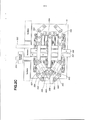
[053] A seguir, será descrita uma montagem exemplificada de três diodos e um condensador snubber que constituem um circuito snubber 32 mostrado na Figura 1. Conforme mostrado na Figura 1, o circuito snubber 321, por exemplo, do elemento de comutação bidirecional 311 tem um terminal conectado ao terminal de entrada do terminal de comutação bidirecional 311, um outro terminal conectado ao terminal intermediário do elemento de comutação bidirecional 311 e ainda um outro terminal conectado ao terminal de saída do elemento de comutação bidirecional 311. Assim, como será entendido a partir das Figuras 2C e 2D, os três diodos são fixados e conectados aos suportes 351 a 356, que são construídos de um corpo condutor elétrico conectado a um terminal intermediário entre cada elemento de comutação bidirecional 31L e o correspondente elemento de comutação bidirecional 31R. Na Figura 2D, apenas o suporte 355 é mostrado.[053] In the following, an exemplary assembly of three diodes and a snubber capacitor will be described which constitute a snubber circuit 32 shown in Figure 1. As shown in Figure 1, the
[054] Neste exemplo, um condensador eletrolítico de tamanho relativamente grande é utilizado como condensador snubber, e o condensador eletrolítico de tamanho relativamente grande é usado como um condensador snubber comum 327 (ver Figura 3) para os seis circuitos snubber 321 a 326. Para a conexão do condensador snubber 327 e os três diodos, são fornecidos os barramentos 347 e 348 que são colocados entre os barramentos 331 e 332 e se estendem na mesma direção que estes barramentos 331 e 332, os barramentos 331 e 332 constituem as linhas de saída P e N.[054] In this example, a relatively large electrolytic capacitor is used as a snubber capacitor, and the relatively large electrolytic capacitor is used as a common 327 snubber capacitor (see Figure 3) for the six
[055] Como pode ser visto a partir das Figuras 2D e 3, os dois barramentos 347 e 348 conectados ao condensador snubber 327 são fixados em uma posição acima dos barramentos 331 e 332, que constituem as linhas de saída de P e N, mas em uma posição inferior aos barramentos 333, 334 e 335. Nota-se que estes dois barramentos 347 e 348 estão apoiados no dissipador de calor 10 ou em uma base (não mostrada ) que não seja o dissipador de calor. Para evitar um curto - circuito nos barramentos 333, 334 e 335, as superfícies exteriores dos barramentos 347 e 348 podem ser revestidos com um material isolante.[055] As can be seen from Figures 2D and 3, the two
[056] A disposição dos barramentos 347 e 348 em relação aos barramentos 331 e 332, que constituem as linhas de saída P e N e o condensador snubber 327 é a seguinte. Isto é, pela disposição dos barramentos 347 e 348 entre os barramentos 331 e 332, tanto a distância do cabeamento até as linhas de saída P e N quanto a distância do cabeamento até o condensador snubber 327 podem ser encurtadas. Além disso, ao se colocar os barramentos 347 e 348 acima dos barramentos 331 e 332, é possível reduzir a distância entre os diodos de cada um dos circuitos snubber 321 a 326.[056] The arrangement of
[057] De acordo com a forma de realização acima referida, as seguintes vantagens são obtidas: 1 ) Neste exemplo, para os seis elementos de comutação bidirecionais 311 a 316 os quais estão dispostos de tal maneira que três elementos e os outros três elementos encontram se respectivamente colocados nos lados esquerdo e direito em relação à linha central CL, são dispostos os seis condensadores de filtro 821 a 825 de tal maneira que os três condensadores e os outros três condensadores são respectivamente colocados nos lados esquerdo e direito em relação à linha central CL, de modo que a distância do cabeamento dos cabos de conexão entre cada um dos condensadores de filtro 821 a 823 e um correspondente dos elementos de comutação bidirecionais 311 a 316 pode ser encurtada. 2 ) Neste exemplo, uma vez que os elementos de comutação bidirecionais pareados 311 e 312, os elementos de comutação bidirecionais pareados 313 e 314 e os elementos de comutação bidirecionais pareados 315 e 316 estão cada um deles dispostos respectivamente nos lados esquerdo e direito em relação à linha central CL, é possível fornecer um layout em que as linhas de saída P e N ( isto é, os barramentos 331 e 332 ) são estabelecidas com a distância mais curta em uma direção. Se o comprimento da disposição do cabeamento através do qual uma corrente CA de alta frequência é transmitida é longo, a disposição é facilmente influenciada pelo componente L. Entretanto, a influência do componente L pode ser eliminada na disposição do cabeamento, de acordo com a invenção. 3 ) Neste exemplo, os seis condensadores de filtro 821 a 826, dos quais três condensadores de filtro e os outros três condensadores de filtro estão dispostos res-pectivamente nos lados esquerdo e direito, são colocados externamente a uma área onde os seis elementos de comutação bidirecionais 311 a 316 são colocados em relação à linha central CL. Assim, a distância na direção esquerda e direita entre o elemento de comutação bidirecional do lado esquerdo 31L e o elemento de comutação bidirecional na lateral direita 31R pode ser encurtada. Por conseguinte, a distância na direção esquerda e direita do dissipador de calor 10 pode ser encurtada, o que pode levar a uma redução em tamanho do dissipador de calor 10. 4 ) Neste exemplo, os terminais de entrada dos elementos de comutação bidirecionais pareados 311 e 312, os terminais de entrada dos elementos de comutação bidirecionais pareados 313 e 314 e os terminais de entrada dos elementos de comutação bidirecionais pareados 315 e 316, os quais estão dispostos no lados esquerdo e direito em relação à linha central CL, estão conectados através dos respectivos barramentos 333, 334 e 335. Deste modo, cada um dos condensadores de filtro 82L e 82R estão dispostos entre as fases que podem ser compartilhadas. Assim, cada condensador de filtro pode ser feito com pequena capacidade, o que resulta em cada condensador de filtro poder ser feito em tamanho pequeno. 5 ) Neste exemplo, uma vez que a direção por onde as linhas de entrada esquerda e direita R, S e T se estendem para a conexão com os elementos de comutação bidirecionais é igual a direção para a linha central CL, uma distância do dissipador de calor 10 na direção esquerda e direita pode ser reduzida. 6 ) Neste exemplo, os condensadores de filtro 821 a 826 estão dispostos nas superfícies superiores dos barramentos, isto é, os condensadores de filtro 821 a 826 são colocados em um lado oposto dos elementos de comutação bidirecionais 311 a 316 em relação ao barramento, o que aumenta o grau de liberdade na concepção do layout dos condensadores de filtro 821 a 826. 7 ) Neste exemplo, a disposição dos barramentos 347 e 348 em relação aos barramentos 331 e 332, que constituem as linhas de saída P e N, e o condensador snubber 327 é feito de modo que os barramentos 347 e 348 estejam colocados entre os barramentos 331 e 332, de modo que tanto a distância do cabeamento até as linhas de saída P e N quanto a distância do cabeamento até o condensador snubber 327 são encurtadas. 8 ) Neste exemplo, uma vez que os barramentos 347 e 348 estão dispostos em uma posição acima dos barramentos 331 e 332, é possível reduzir a distância entre os diodos de cada um dos circuitos snubber 321 a 326. 9 ) Neste exemplo, uma vez que os três condensadores de filtro 821, 822 e 823 estão colocados nos vértices do triângulo, o comprimento do cabeamento entre os condensadores pode ser encurtado e, assim, o conversor de energia 3 pode ser feito em tamanho pequeno, e a sincronização entre os condensadores pode ser assegurada. 10 ) Neste exemplo, uma vez que o vértice do triângulo, no qual um dos três condensadores de filtro está disposto, está dirigido para fora, o balanço do cabeamento dos condensadores é melhorado em comparação com uma disposição, na qual o vértice está dirigido para dentro e as distâncias até os barramentos 333, 334 e 335 podem ser encurtadas. 11 ) Neste exemplo, uma vez que os barramentos 342 e 343 estão dispostos de modo a estarem angulados em relação à linha que conecta os terminais de entrada dos elementos de comutação bidirecionais 311, 313 e 315, a distância do cabeamento entre os condensadores de filtro pode ser finamente equalizada com a distância do cabeamento dos condensador de filtro 823 disposto entre a fase R e a fase T. Assim, a sincronização entre os condensadores de filtro 821, 822 e 823 pode ser assegurada. 12 ) Neste exemplo, uma vez que os barramentos 342 e 343 estão dispostos de modo a se afastarem da linha que conecta os terminais de entrada dos elementos de comutação bidirecionais 311, 313 e 315, a distância de conexão entre os condensadores de filtro 821 e 822 e os barramentos 333, 334 e 335 pode ser reduzida e, assim, o conversor de energia 3 pode ser feito em tamanho pequeno. Outras formas de realização A presente invenção tem outras modificações e concretizações da forma de realização acima mencionada. As modificações da invenção serão descritas a seguir. A presente invenção não está limitada à forma de realização acima referida e às formas de realização seguintes. Em seguida, as peças idênticas às descritas na forma de realização acima mencionada estão indicadas pela mesma referência numérica e a explicação sobre as mesmas peças será apropriadamente omitida.[057] According to the aforementioned embodiment, the following advantages are obtained: 1) In this example, for the six
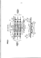
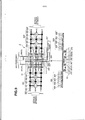
[058] Na forma de realização acima referida, tal como é mostrado na Figura 3, os três condensadores de filtro do lado esquerdo 82L e os três condensadores de filtro do lado direito 82R estão dispostos externamente a uma área dos elementos de comutação bidirecionais 311, 313 e 315 e uma área de elementos de comutação bidirecionais 312, 314 e 316, respectivamente, em relação à linha central CL. No entanto, como é visto a partir das Figuras 4A e 4B, os três condensadores de filtro do lado esquerdo e os três condensadores do lado direito podem ser dispostos entre uma área dos elementos de comutação bidirecionais do lado esquerdo 311, 313 e 315 e uma área dos elementos de comutação bidirecionais do lado direito 312, 314 e 316, em relação à linha central CL.[058] In the above-mentioned embodiment, as shown in Figure 3, the three filter capacitors on the
[059] Na forma de realização acima referida, tal como é mostrado na Figura 3, os seis elementos de comutação bidirecionais 311 a 316 estão dispostos de maneira que os elementos de comutação bidirecionais 311, 313 e 315 e os elementos de comutação bidirecionais 312, 314 e 316 estão dispostos respectivamente nos lados esquerdo e direito em relação à linha central CL. No entanto, como é mostrado na Figura 5, os elementos de comutação bidirecionais 311, 313 e 315 e os elementos de comutação bidirecionais 312, 314 e 316 podem ser dispostos ao longo da linha central CL.[059] In the aforementioned embodiment, as shown in Figure 3, the six
[060] Na forma de realização acima referida, tal como é mostrado na Figura 3, os seis elementos de comutação bidirecionais 311 a 316 estão dispostos de maneira que os elementos de comutação bidirecionais 311, 313 e 315 e os elementos de comutação bidirecionais 312, 314 e 316 estão dispostos respectivamente nos lados esquerdo e direito em relação à linha central CL e os terminais de entrada e de saída dos elementos de comutação bidirecionais do lado esquerdo e os terminais de entrada e de saída dos elementos de comutação bidirecionais do lado direito estão dispostos simetricamente em relação à linha central CL. No entanto, como é mostrada na Figura 6, uma disposição pode ser empregada na qual os elementos de comutação bidirecionais 311, 313 e 315 e os elementos de comutação bidirecionais 312, 314 e 316 estão dispostos nos lados esquerdo e direito em relação à linha central CL e os terminais de entrada e de saída dos elementos de comutação bidirecionais do lado esquerdo e os terminais de entrada e de saída dos elementos de comutação bidirecionais do lado direito estão dispostos da mesma maneira. Neste caso, as linhas de entrada R, S e T do sistema duplo estão conectadas aos terminais de entrada dos elementos de comutação bidirecionais do lado esquerdo e direito, enquanto se estendem na mesma direção (na direção da esquerda para a direita, no exemplo ilustrado).[060] In the aforementioned embodiment, as shown in Figure 3, the six
[061] Na forma de realização acima referida, tal como é mostrado na Figura 3, os condensadores de filtro 821 a 826 estão dispostos entre as fases, enquanto mantém a relação um-para-um com os seis elementos de comutação bidirecionais 311 a 316. No entanto, como é mostrado na Figura 7, uma disposição pode ser utilizada na qual os condensadores de filtro 821 a 826 estão dispostos entre as fases, de tal maneira que muitos ( dois no exemplo ilustrado ) dos condensadores de filtro 821 a 826 estão conectados a cada um dos seis elementos de comutação bidirecionais 311 a 316.[061] In the above-mentioned embodiment, as shown in Figure 3,
[062] Neste caso, os condensadores de filtro podem estar dispostos no centro do conversor de energia 3, tal como é mostrado na Figura 8, ou do lado de fora do conversor de energia 3, como é mostrado na Figura 9. Como será entendido a partir da Figura 8, quando os condensadores de filtro estão dispostos no centro do conversor de energia 3, os espaços vazios são utilizáveis, de modo que o tamanho do conversor de energia 3 pode ser tão pequeno quanto for possível.[062] In this case, the filter capacitors can be arranged in the center of the
[063] Os elementos de comutação bidirecionais acima mencionados 311, 313 e 315 correspondem aos primeiros elementos de comutação nas reivindicações, os elementos de comutação bidirecionais acima mencionados 312, 314 e 316 correspondem aos segundos elementos de comutação nas reivindicações, o conversor de energia 3 acima mencionado corresponde a um circuito conversor nas reivindicações, os condensadores de filtro acima mencionados 821 a 826 e 831 a 836 correspondem aos condensadores nas reivindicações e os barramentos acima mencionados 331 e 332 correspondem às linhas de saída nas reivindicações.[063] The aforementioned two-
Claims (7)
Applications Claiming Priority (3)
| Application Number | Priority Date | Filing Date | Title |
|---|---|---|---|
| JP2011-122842 | 2011-05-31 | ||
| JP2011122842A JP5377574B2 (en) | 2011-05-31 | 2011-05-31 | Power converter |
| PCT/JP2012/061658 WO2012165103A1 (en) | 2011-05-31 | 2012-05-07 | Power conversion device |
Publications (2)
| Publication Number | Publication Date |
|---|---|
| BR112013030560A2 BR112013030560A2 (en) | 2016-09-27 |
| BR112013030560B1 true BR112013030560B1 (en) | 2020-11-03 |
Family
ID=47258967
Family Applications (1)
| Application Number | Title | Priority Date | Filing Date |
|---|---|---|---|
| BR112013030560-6A BR112013030560B1 (en) | 2011-05-31 | 2012-05-07 | power converter that directly converts polyphase ac current to ac current |
Country Status (9)
| Country | Link |
|---|---|
| US (1) | US9490721B2 (en) |
| EP (1) | EP2717452B1 (en) |
| JP (1) | JP5377574B2 (en) |
| CN (1) | CN103650317B (en) |
| BR (1) | BR112013030560B1 (en) |
| MX (1) | MX2013013987A (en) |
| MY (1) | MY158683A (en) |
| RU (1) | RU2557561C1 (en) |
| WO (1) | WO2012165103A1 (en) |
Families Citing this family (7)
| Publication number | Priority date | Publication date | Assignee | Title |
|---|---|---|---|---|
| JP5437312B2 (en) | 2011-05-31 | 2014-03-12 | 日産自動車株式会社 | Power converter |
| JP5377575B2 (en) * | 2011-05-31 | 2013-12-25 | 日産自動車株式会社 | Power converter |
| JP5476510B2 (en) * | 2011-10-07 | 2014-04-23 | 日産自動車株式会社 | Power converter |
| EP2765700B1 (en) * | 2011-10-07 | 2017-04-26 | Nissan Motor Co., Ltd | Power converter |
| WO2017038294A1 (en) * | 2015-08-28 | 2017-03-09 | 株式会社村田製作所 | Dc-dc converter |
| RU176542U1 (en) * | 2017-02-07 | 2018-01-23 | Открытое акционерное общество "Электровыпрямитель" | Device for generating control pulses of a diode-thyristor bridge |
| JP6488421B1 (en) * | 2018-09-12 | 2019-03-20 | 高周波熱錬株式会社 | Snubber circuit, power semiconductor module, and induction heating power supply device |
Family Cites Families (48)
| Publication number | Priority date | Publication date | Assignee | Title |
|---|---|---|---|---|
| US4363065A (en) * | 1979-02-08 | 1982-12-07 | Uohiko Hasegawa | Interphase unbalance detector for AC load circuit |
| US4468725A (en) * | 1982-06-18 | 1984-08-28 | Texas Instruments Incorporated | Direct AC converter for converting a balanced AC polyphase input to an output voltage |
| US4833584A (en) * | 1987-10-16 | 1989-05-23 | Wisconsin Alumni Research Foundation | Quasi-resonant current mode static power conversion method and apparatus |
| JP2704519B2 (en) * | 1988-03-09 | 1998-01-26 | オリジン電気株式会社 | DC power supply |
| JPH0628292B2 (en) | 1988-11-11 | 1994-04-13 | 富士電機株式会社 | Reverse blocking transistor module |
| US5010471A (en) * | 1989-06-26 | 1991-04-23 | Robert F. Frijouf | Three-phase AC-to-AC series resonant power converter with reduced number of switches |
| JP2719012B2 (en) * | 1989-10-31 | 1998-02-25 | 三菱電機株式会社 | Inverter device |
| GB2242580B (en) | 1990-03-30 | 1994-06-15 | Mitsubishi Electric Corp | Inverter unit with improved bus-plate configuration |
| DE69210940T2 (en) * | 1991-10-21 | 1996-11-14 | Toshiba Kawasaki Kk | Power converter |
| JP2896454B2 (en) * | 1992-11-25 | 1999-05-31 | 株式会社日立製作所 | Inverter device |
| JP3195105B2 (en) * | 1993-02-26 | 2001-08-06 | 株式会社東芝 | DC power supply circuit for multi-phase input |
| JPH06261556A (en) | 1993-03-04 | 1994-09-16 | Toshiba Corp | Semiconductor switch apparatus |
| US5517063A (en) | 1994-06-10 | 1996-05-14 | Westinghouse Electric Corp. | Three phase power bridge assembly |
| SE9500761D0 (en) | 1995-03-02 | 1995-03-02 | Abb Research Ltd | Protection circuit for series-connected power semiconductors |
| US6266258B1 (en) | 1995-09-29 | 2001-07-24 | Rockwell Technologies, Llc | Power substrate element topology |
| FI110370B (en) | 1998-07-31 | 2002-12-31 | Lexel Finland Ab Oy | Arrangement to eliminate radio interference from electronic power regulator |
| JP2001045772A (en) * | 1999-08-03 | 2001-02-16 | Yaskawa Electric Corp | 3-level inverter or pwn cycloconverter |
| DE10014641C2 (en) | 2000-03-24 | 2002-03-07 | Siemens Ag | Circuit arrangement with a bidirectional circuit breaker in common collector mode and with an active overvoltage protection device |
| DE10037970A1 (en) | 2000-08-03 | 2002-03-07 | Siemens Ag | Low induction busbar for a matrix converter |
| JP3793407B2 (en) | 2000-09-19 | 2006-07-05 | 株式会社日立製作所 | Power converter |
| JP4501145B2 (en) * | 2001-02-23 | 2010-07-14 | Tdkラムダ株式会社 | Three-phase noise filter |
| JP4337443B2 (en) * | 2003-08-12 | 2009-09-30 | 株式会社日立製作所 | Matrix converter system |
| JP4293000B2 (en) | 2004-01-29 | 2009-07-08 | 株式会社日立製作所 | Power converter |
| JP4296960B2 (en) * | 2004-02-20 | 2009-07-15 | 株式会社日立製作所 | Power converter |
| JP4807516B2 (en) | 2004-09-29 | 2011-11-02 | 株式会社安川電機 | Parallel multiple matrix converter device |
| JP4581777B2 (en) | 2005-03-24 | 2010-11-17 | トヨタ自動車株式会社 | Power module |
| JP4765017B2 (en) * | 2005-05-25 | 2011-09-07 | 富士電機株式会社 | AC-AC power converter |
| US7969755B2 (en) * | 2005-09-09 | 2011-06-28 | Siemens Aktiengesellschaft | Apparatus for electrical power transmission |
| KR20080094917A (en) * | 2006-02-17 | 2008-10-27 | 가부시키가이샤 야스카와덴키 | Power converter provided with bus bar |
| JP4793096B2 (en) * | 2006-05-24 | 2011-10-12 | 株式会社明電舎 | High voltage AC direct power converter |
| CN101523710B (en) * | 2006-06-06 | 2014-03-05 | 威廉·亚历山大 | Universal power converter |
| US8008805B2 (en) | 2006-12-07 | 2011-08-30 | Nissan Motor Co., Ltd. | Power conversion apparatus and motor drive system |
| JP4720756B2 (en) | 2007-02-22 | 2011-07-13 | トヨタ自動車株式会社 | Semiconductor power conversion device and manufacturing method thereof |
| US7573732B2 (en) | 2007-05-25 | 2009-08-11 | General Electric Company | Protective circuit and method for multi-level converter |
| US20090052134A1 (en) | 2007-08-22 | 2009-02-26 | Casteel Jordan B | Liquid-cooled grounded heatsink for diode rectifier system |
| JP4640423B2 (en) | 2008-03-04 | 2011-03-02 | 株式会社豊田自動織機 | Power converter |
| US8031479B2 (en) | 2008-03-04 | 2011-10-04 | Kabushiki Kaisha Toyota Jidoshokki | Power converter apparatus |
| CN101540580B (en) * | 2008-03-18 | 2012-03-14 | 新能动力(北京)电气科技有限公司 | Electric energy feedback device |
| CN102047545B (en) * | 2008-05-30 | 2014-12-10 | 株式会社安川电机 | Control device for matrix converter and output voltage generating method thereof |
| JP5586872B2 (en) * | 2009-05-07 | 2014-09-10 | 電気興業株式会社 | Three-phase single-phase direct power converter circuit |
| EP2296156A1 (en) | 2009-08-13 | 2011-03-16 | ABB Research Ltd | Composite capacitance and use thereof |
| US8411474B2 (en) | 2010-04-30 | 2013-04-02 | General Electric Company | System and method for protection of a multilevel converter |
| JP5590448B2 (en) * | 2010-07-20 | 2014-09-17 | 株式会社安川電機 | Matrix converter |
| JP2012054449A (en) | 2010-09-02 | 2012-03-15 | Aisin Aw Co Ltd | Electric connection device |
| EP2512023A3 (en) | 2011-04-14 | 2017-06-28 | General Electric Technology GmbH | Power converter arrangement and method for operating a power converter arrangement |
| JP5476510B2 (en) | 2011-10-07 | 2014-04-23 | 日産自動車株式会社 | Power converter |
| EP2765700B1 (en) | 2011-10-07 | 2017-04-26 | Nissan Motor Co., Ltd | Power converter |
| MX339716B (en) * | 2011-12-19 | 2016-06-07 | Ensync Inc | System and method for low speed control of polyphase ac machine. |
-
2011
- 2011-05-31 JP JP2011122842A patent/JP5377574B2/en active Active
-
2012
- 2012-05-07 RU RU2013158883/07A patent/RU2557561C1/en active
- 2012-05-07 MY MYPI2013004131A patent/MY158683A/en unknown
- 2012-05-07 EP EP12792428.0A patent/EP2717452B1/en active Active
- 2012-05-07 BR BR112013030560-6A patent/BR112013030560B1/en active IP Right Grant
- 2012-05-07 WO PCT/JP2012/061658 patent/WO2012165103A1/en active Application Filing
- 2012-05-07 CN CN201280025374.8A patent/CN103650317B/en active Active
- 2012-05-07 MX MX2013013987A patent/MX2013013987A/en active IP Right Grant
- 2012-05-07 US US14/122,268 patent/US9490721B2/en active Active
Also Published As
| Publication number | Publication date |
|---|---|
| BR112013030560A2 (en) | 2016-09-27 |
| MY158683A (en) | 2016-10-31 |
| RU2557561C1 (en) | 2015-07-27 |
| MX2013013987A (en) | 2014-05-27 |
| CN103650317B (en) | 2016-06-22 |
| EP2717452A4 (en) | 2015-11-25 |
| EP2717452B1 (en) | 2021-03-10 |
| US20140085950A1 (en) | 2014-03-27 |
| EP2717452A1 (en) | 2014-04-09 |
| CN103650317A (en) | 2014-03-19 |
| RU2013158883A (en) | 2015-07-10 |
| JP2012253856A (en) | 2012-12-20 |
| WO2012165103A1 (en) | 2012-12-06 |
| US9490721B2 (en) | 2016-11-08 |
| JP5377574B2 (en) | 2013-12-25 |
Similar Documents
| Publication | Publication Date | Title |
|---|---|---|
| BR112013030560B1 (en) | power converter that directly converts polyphase ac current to ac current | |
| BR112013030557B1 (en) | power converter | |
| BR112013030558B1 (en) | energy conversion appliance | |
| RU2556245C1 (en) | Energy conversion unit | |
| RU2556243C1 (en) | Power conversion device | |
| BR112013030561B1 (en) | energy conversion apparatus for converting polyphasic ac energy directly into ac energy | |
| WO2013051476A1 (en) | Power converter | |
| JPWO2013051475A1 (en) | Power converter | |
| BR112013030559B1 (en) | POWER CONVERTER |
Legal Events
| Date | Code | Title | Description |
|---|---|---|---|
| B06F | Objections, documents and/or translations needed after an examination request according [chapter 6.6 patent gazette] | ||
| B06U | Preliminary requirement: requests with searches performed by other patent offices: procedure suspended [chapter 6.21 patent gazette] | ||
| B09A | Decision: intention to grant [chapter 9.1 patent gazette] | ||
| B16A | Patent or certificate of addition of invention granted [chapter 16.1 patent gazette] |
Free format text: PRAZO DE VALIDADE: 20 (VINTE) ANOS CONTADOS A PARTIR DE 07/05/2012, OBSERVADAS AS CONDICOES LEGAIS. |