WO2012157449A1 - Semiconductor device, solar cell module, solar cell string, and solar cell array - Google Patents
Semiconductor device, solar cell module, solar cell string, and solar cell array Download PDFInfo
- Publication number
- WO2012157449A1 WO2012157449A1 PCT/JP2012/061547 JP2012061547W WO2012157449A1 WO 2012157449 A1 WO2012157449 A1 WO 2012157449A1 JP 2012061547 W JP2012061547 W JP 2012061547W WO 2012157449 A1 WO2012157449 A1 WO 2012157449A1
- Authority
- WO
- WIPO (PCT)
- Prior art keywords
- solar cell
- semiconductor
- photoelectric conversion
- layer
- substrate
- Prior art date
Links
- 239000004065 semiconductor Substances 0.000 title claims abstract description 144
- 239000000758 substrate Substances 0.000 claims abstract description 168
- 239000004020 conductor Substances 0.000 claims abstract description 21
- 238000006243 chemical reaction Methods 0.000 claims description 138
- 229910052782 aluminium Inorganic materials 0.000 claims description 16
- 239000002131 composite material Substances 0.000 claims description 15
- 239000010409 thin film Substances 0.000 claims description 15
- XAGFODPZIPBFFR-UHFFFAOYSA-N aluminium Chemical compound [Al] XAGFODPZIPBFFR-UHFFFAOYSA-N 0.000 claims description 14
- 229910052711 selenium Inorganic materials 0.000 claims description 14
- 238000003491 array Methods 0.000 claims description 12
- 150000001875 compounds Chemical class 0.000 claims description 10
- 229910052802 copper Inorganic materials 0.000 claims description 6
- 229910052738 indium Inorganic materials 0.000 claims description 6
- 229910004613 CdTe Inorganic materials 0.000 claims description 5
- 229910052733 gallium Inorganic materials 0.000 claims description 5
- 229910000831 Steel Inorganic materials 0.000 claims description 4
- 238000007743 anodising Methods 0.000 claims description 4
- 229910052710 silicon Inorganic materials 0.000 claims description 4
- 239000010935 stainless steel Substances 0.000 claims description 4
- 229910001220 stainless steel Inorganic materials 0.000 claims description 4
- 239000010959 steel Substances 0.000 claims description 4
- 229910052717 sulfur Inorganic materials 0.000 claims description 4
- DVRDHUBQLOKMHZ-UHFFFAOYSA-N chalcopyrite Chemical group [S-2].[S-2].[Fe+2].[Cu+2] DVRDHUBQLOKMHZ-UHFFFAOYSA-N 0.000 claims description 3
- XUIMIQQOPSSXEZ-UHFFFAOYSA-N Silicon Chemical compound [Si] XUIMIQQOPSSXEZ-UHFFFAOYSA-N 0.000 claims description 2
- 239000010703 silicon Substances 0.000 claims description 2
- 229910052709 silver Inorganic materials 0.000 claims description 2
- 229910052714 tellurium Inorganic materials 0.000 claims description 2
- 239000010410 layer Substances 0.000 description 225
- 238000000034 method Methods 0.000 description 64
- 239000010408 film Substances 0.000 description 41
- 238000010248 power generation Methods 0.000 description 30
- 239000011669 selenium Substances 0.000 description 26
- 238000009413 insulation Methods 0.000 description 23
- 229910000679 solder Inorganic materials 0.000 description 19
- 229910052751 metal Inorganic materials 0.000 description 18
- 239000002184 metal Substances 0.000 description 17
- 230000005684 electric field Effects 0.000 description 16
- 239000010949 copper Substances 0.000 description 15
- 238000010438 heat treatment Methods 0.000 description 11
- 238000004544 sputter deposition Methods 0.000 description 11
- 239000010407 anodic oxide Substances 0.000 description 10
- 229910045601 alloy Inorganic materials 0.000 description 9
- 239000000956 alloy Substances 0.000 description 9
- 238000004519 manufacturing process Methods 0.000 description 9
- 239000000463 material Substances 0.000 description 9
- 229910021417 amorphous silicon Inorganic materials 0.000 description 8
- BUGBHKTXTAQXES-UHFFFAOYSA-N Selenium Chemical compound [Se] BUGBHKTXTAQXES-UHFFFAOYSA-N 0.000 description 6
- 238000009210 therapy by ultrasound Methods 0.000 description 6
- 238000007740 vapor deposition Methods 0.000 description 5
- 238000010586 diagram Methods 0.000 description 4
- 238000009792 diffusion process Methods 0.000 description 4
- 239000012535 impurity Substances 0.000 description 4
- 239000012811 non-conductive material Substances 0.000 description 4
- 230000003647 oxidation Effects 0.000 description 4
- 238000007254 oxidation reaction Methods 0.000 description 4
- 239000002243 precursor Substances 0.000 description 4
- 230000008569 process Effects 0.000 description 4
- 238000005476 soldering Methods 0.000 description 4
- 239000007790 solid phase Substances 0.000 description 4
- 230000015572 biosynthetic process Effects 0.000 description 3
- 238000010549 co-Evaporation Methods 0.000 description 3
- 238000009826 distribution Methods 0.000 description 3
- 238000005868 electrolysis reaction Methods 0.000 description 3
- 239000007789 gas Substances 0.000 description 3
- WABPQHHGFIMREM-UHFFFAOYSA-N lead(0) Chemical compound [Pb] WABPQHHGFIMREM-UHFFFAOYSA-N 0.000 description 3
- 230000031700 light absorption Effects 0.000 description 3
- 230000002093 peripheral effect Effects 0.000 description 3
- 238000007650 screen-printing Methods 0.000 description 3
- 239000010936 titanium Substances 0.000 description 3
- 229910052719 titanium Inorganic materials 0.000 description 3
- 229910000838 Al alloy Inorganic materials 0.000 description 2
- 229910001374 Invar Inorganic materials 0.000 description 2
- RPPBZEBXAAZZJH-UHFFFAOYSA-N cadmium telluride Chemical compound [Te]=[Cd] RPPBZEBXAAZZJH-UHFFFAOYSA-N 0.000 description 2
- 229910052804 chromium Inorganic materials 0.000 description 2
- 239000011248 coating agent Substances 0.000 description 2
- 238000000576 coating method Methods 0.000 description 2
- 239000012141 concentrate Substances 0.000 description 2
- 238000005566 electron beam evaporation Methods 0.000 description 2
- 238000002488 metal-organic chemical vapour deposition Methods 0.000 description 2
- 239000000203 mixture Substances 0.000 description 2
- 229910052750 molybdenum Inorganic materials 0.000 description 2
- 239000002994 raw material Substances 0.000 description 2
- 239000011347 resin Substances 0.000 description 2
- 229920005989 resin Polymers 0.000 description 2
- 239000002356 single layer Substances 0.000 description 2
- 238000005987 sulfurization reaction Methods 0.000 description 2
- 229910052725 zinc Inorganic materials 0.000 description 2
- 229910018134 Al-Mg Inorganic materials 0.000 description 1
- 229910021365 Al-Mg-Si alloy Inorganic materials 0.000 description 1
- 229910018131 Al-Mn Inorganic materials 0.000 description 1
- 229910021364 Al-Si alloy Inorganic materials 0.000 description 1
- 229910018467 Al—Mg Inorganic materials 0.000 description 1
- 229910018461 Al—Mn Inorganic materials 0.000 description 1
- 229910018580 Al—Zr Inorganic materials 0.000 description 1
- RYGMFSIKBFXOCR-UHFFFAOYSA-N Copper Chemical compound [Cu] RYGMFSIKBFXOCR-UHFFFAOYSA-N 0.000 description 1
- 229910000807 Ga alloy Inorganic materials 0.000 description 1
- 229910001218 Gallium arsenide Inorganic materials 0.000 description 1
- 101000651021 Homo sapiens Splicing factor, arginine/serine-rich 19 Proteins 0.000 description 1
- 229910001209 Low-carbon steel Inorganic materials 0.000 description 1
- 229910000861 Mg alloy Inorganic materials 0.000 description 1
- ZOKXTWBITQBERF-UHFFFAOYSA-N Molybdenum Chemical compound [Mo] ZOKXTWBITQBERF-UHFFFAOYSA-N 0.000 description 1
- 239000004642 Polyimide Substances 0.000 description 1
- 229910006404 SnO 2 Inorganic materials 0.000 description 1
- 102100027779 Splicing factor, arginine/serine-rich 19 Human genes 0.000 description 1
- RTAQQCXQSZGOHL-UHFFFAOYSA-N Titanium Chemical compound [Ti] RTAQQCXQSZGOHL-UHFFFAOYSA-N 0.000 description 1
- 229910003363 ZnMgO Inorganic materials 0.000 description 1
- LEVVHYCKPQWKOP-UHFFFAOYSA-N [Si].[Ge] Chemical compound [Si].[Ge] LEVVHYCKPQWKOP-UHFFFAOYSA-N 0.000 description 1
- 239000010953 base metal Substances 0.000 description 1
- 230000008901 benefit Effects 0.000 description 1
- 229910052796 boron Inorganic materials 0.000 description 1
- 229910052791 calcium Inorganic materials 0.000 description 1
- 230000015556 catabolic process Effects 0.000 description 1
- 229910052951 chalcopyrite Inorganic materials 0.000 description 1
- 238000004140 cleaning Methods 0.000 description 1
- 239000000470 constituent Substances 0.000 description 1
- 239000013078 crystal Substances 0.000 description 1
- 238000006731 degradation reaction Methods 0.000 description 1
- 238000000151 deposition Methods 0.000 description 1
- 230000008021 deposition Effects 0.000 description 1
- 230000005611 electricity Effects 0.000 description 1
- 239000008151 electrolyte solution Substances 0.000 description 1
- 230000007613 environmental effect Effects 0.000 description 1
- 238000005530 etching Methods 0.000 description 1
- 238000002474 experimental method Methods 0.000 description 1
- 239000010419 fine particle Substances 0.000 description 1
- 239000011521 glass Substances 0.000 description 1
- AMGQUBHHOARCQH-UHFFFAOYSA-N indium;oxotin Chemical compound [In].[Sn]=O AMGQUBHHOARCQH-UHFFFAOYSA-N 0.000 description 1
- 229910052742 iron Inorganic materials 0.000 description 1
- 229910000833 kovar Inorganic materials 0.000 description 1
- 229910052749 magnesium Inorganic materials 0.000 description 1
- 238000001755 magnetron sputter deposition Methods 0.000 description 1
- 229910052748 manganese Inorganic materials 0.000 description 1
- 238000002844 melting Methods 0.000 description 1
- 230000008018 melting Effects 0.000 description 1
- 229910021424 microcrystalline silicon Inorganic materials 0.000 description 1
- 238000002156 mixing Methods 0.000 description 1
- 238000012986 modification Methods 0.000 description 1
- 230000004048 modification Effects 0.000 description 1
- 239000011733 molybdenum Substances 0.000 description 1
- 229910052698 phosphorus Inorganic materials 0.000 description 1
- 230000001443 photoexcitation Effects 0.000 description 1
- 238000005498 polishing Methods 0.000 description 1
- 229920001721 polyimide Polymers 0.000 description 1
- 239000000843 powder Substances 0.000 description 1
- 238000001552 radio frequency sputter deposition Methods 0.000 description 1
- 230000009467 reduction Effects 0.000 description 1
- 150000003839 salts Chemical class 0.000 description 1
- SPVXKVOXSXTJOY-UHFFFAOYSA-N selane Chemical compound [SeH2] SPVXKVOXSXTJOY-UHFFFAOYSA-N 0.000 description 1
- 229910000058 selane Inorganic materials 0.000 description 1
- 229940065287 selenium compound Drugs 0.000 description 1
- 150000003343 selenium compounds Chemical class 0.000 description 1
- 230000035939 shock Effects 0.000 description 1
- 238000004088 simulation Methods 0.000 description 1
- 238000003980 solgel method Methods 0.000 description 1
- 239000000243 solution Substances 0.000 description 1
- 238000000527 sonication Methods 0.000 description 1
- 239000007921 spray Substances 0.000 description 1
- 238000005507 spraying Methods 0.000 description 1
- 238000000859 sublimation Methods 0.000 description 1
- 230000008022 sublimation Effects 0.000 description 1
- 239000000126 substance Substances 0.000 description 1
- 229910021654 trace metal Inorganic materials 0.000 description 1
- 239000012808 vapor phase Substances 0.000 description 1
- 239000011800 void material Substances 0.000 description 1
- 238000003466 welding Methods 0.000 description 1
Images


Classifications
-
- H—ELECTRICITY
- H01—ELECTRIC ELEMENTS
- H01L—SEMICONDUCTOR DEVICES NOT COVERED BY CLASS H10
- H01L31/00—Semiconductor devices sensitive to infrared radiation, light, electromagnetic radiation of shorter wavelength or corpuscular radiation and specially adapted either for the conversion of the energy of such radiation into electrical energy or for the control of electrical energy by such radiation; Processes or apparatus specially adapted for the manufacture or treatment thereof or of parts thereof; Details thereof
- H01L31/02—Details
- H01L31/02002—Arrangements for conducting electric current to or from the device in operations
- H01L31/02005—Arrangements for conducting electric current to or from the device in operations for device characterised by at least one potential jump barrier or surface barrier
- H01L31/02008—Arrangements for conducting electric current to or from the device in operations for device characterised by at least one potential jump barrier or surface barrier for solar cells or solar cell modules
-
- H—ELECTRICITY
- H01—ELECTRIC ELEMENTS
- H01L—SEMICONDUCTOR DEVICES NOT COVERED BY CLASS H10
- H01L31/00—Semiconductor devices sensitive to infrared radiation, light, electromagnetic radiation of shorter wavelength or corpuscular radiation and specially adapted either for the conversion of the energy of such radiation into electrical energy or for the control of electrical energy by such radiation; Processes or apparatus specially adapted for the manufacture or treatment thereof or of parts thereof; Details thereof
- H01L31/04—Semiconductor devices sensitive to infrared radiation, light, electromagnetic radiation of shorter wavelength or corpuscular radiation and specially adapted either for the conversion of the energy of such radiation into electrical energy or for the control of electrical energy by such radiation; Processes or apparatus specially adapted for the manufacture or treatment thereof or of parts thereof; Details thereof adapted as photovoltaic [PV] conversion devices
- H01L31/042—PV modules or arrays of single PV cells
- H01L31/0445—PV modules or arrays of single PV cells including thin film solar cells, e.g. single thin film a-Si, CIS or CdTe solar cells
- H01L31/046—PV modules composed of a plurality of thin film solar cells deposited on the same substrate
-
- H—ELECTRICITY
- H01—ELECTRIC ELEMENTS
- H01L—SEMICONDUCTOR DEVICES NOT COVERED BY CLASS H10
- H01L31/00—Semiconductor devices sensitive to infrared radiation, light, electromagnetic radiation of shorter wavelength or corpuscular radiation and specially adapted either for the conversion of the energy of such radiation into electrical energy or for the control of electrical energy by such radiation; Processes or apparatus specially adapted for the manufacture or treatment thereof or of parts thereof; Details thereof
- H01L31/04—Semiconductor devices sensitive to infrared radiation, light, electromagnetic radiation of shorter wavelength or corpuscular radiation and specially adapted either for the conversion of the energy of such radiation into electrical energy or for the control of electrical energy by such radiation; Processes or apparatus specially adapted for the manufacture or treatment thereof or of parts thereof; Details thereof adapted as photovoltaic [PV] conversion devices
- H01L31/042—PV modules or arrays of single PV cells
- H01L31/05—Electrical interconnection means between PV cells inside the PV module, e.g. series connection of PV cells
- H01L31/0504—Electrical interconnection means between PV cells inside the PV module, e.g. series connection of PV cells specially adapted for series or parallel connection of solar cells in a module
-
- H—ELECTRICITY
- H01—ELECTRIC ELEMENTS
- H01L—SEMICONDUCTOR DEVICES NOT COVERED BY CLASS H10
- H01L2924/00—Indexing scheme for arrangements or methods for connecting or disconnecting semiconductor or solid-state bodies as covered by H01L24/00
- H01L2924/0001—Technical content checked by a classifier
- H01L2924/0002—Not covered by any one of groups H01L24/00, H01L24/00 and H01L2224/00
-
- Y—GENERAL TAGGING OF NEW TECHNOLOGICAL DEVELOPMENTS; GENERAL TAGGING OF CROSS-SECTIONAL TECHNOLOGIES SPANNING OVER SEVERAL SECTIONS OF THE IPC; TECHNICAL SUBJECTS COVERED BY FORMER USPC CROSS-REFERENCE ART COLLECTIONS [XRACs] AND DIGESTS
- Y02—TECHNOLOGIES OR APPLICATIONS FOR MITIGATION OR ADAPTATION AGAINST CLIMATE CHANGE
- Y02E—REDUCTION OF GREENHOUSE GAS [GHG] EMISSIONS, RELATED TO ENERGY GENERATION, TRANSMISSION OR DISTRIBUTION
- Y02E10/00—Energy generation through renewable energy sources
- Y02E10/50—Photovoltaic [PV] energy
- Y02E10/541—CuInSe2 material PV cells
-
- Y—GENERAL TAGGING OF NEW TECHNOLOGICAL DEVELOPMENTS; GENERAL TAGGING OF CROSS-SECTIONAL TECHNOLOGIES SPANNING OVER SEVERAL SECTIONS OF THE IPC; TECHNICAL SUBJECTS COVERED BY FORMER USPC CROSS-REFERENCE ART COLLECTIONS [XRACs] AND DIGESTS
- Y02—TECHNOLOGIES OR APPLICATIONS FOR MITIGATION OR ADAPTATION AGAINST CLIMATE CHANGE
- Y02P—CLIMATE CHANGE MITIGATION TECHNOLOGIES IN THE PRODUCTION OR PROCESSING OF GOODS
- Y02P70/00—Climate change mitigation technologies in the production process for final industrial or consumer products
- Y02P70/50—Manufacturing or production processes characterised by the final manufactured product
Definitions
- the present invention relates to a semiconductor device, a solar cell module, a solar cell string, and a solar cell array, and more particularly, in a semiconductor device, a semiconductor element having improved insulation between a conductive substrate made of a conductive material and a semiconductor element.
- the present invention relates to an arrangement method and a solar cell module, a solar cell string, and a solar cell array using the semiconductor element.
- a substrate made of a conductive material such as a metal or alloy having the characteristics of lightness and flexibility may be applicable to a wide range of applications. Further, since the substrate made of the conductive material can withstand high temperature processes, it can be applied to a semiconductor that cannot be handled by a resin substrate such as polyimide. For example, if it is used as a substrate for a solar cell, the photoelectric conversion efficiency can be improved, and high efficiency of the solar cell can be expected.
- an insulating layer is provided on at least one surface of a substrate made of a conductive material.
- an oxide obtained by anodizing a substrate material is used (for example, Patent Document 1).
- Patent Document 1 discloses that the potential in the vicinity of the middle of series-connected elements (that is, solar cells) and the potential of the substrate made of a conductive material (metal substrate) are made equipotential. Accordingly, it is disclosed that the potential difference between the element and the substrate is reduced.
- FIGS. 7A and 7B show the results of simulating the state of electrolytic concentration at the electrode corners.
- FIG. 7A shows the result when the curvature of the corner is changed
- FIG. 7B shows the result when the angle of the corner is changed. From FIG. 7A, it can be seen that the electric field E max at the electrode end portion having a diameter of 25 mm (corresponding to the electrode corner portion having a curvature radius of 12.5 mm) is about 1.3 times the electric field E 0 at the center portion of the electrode.
- Patent Document 4 discloses that a wiring arrangement is devised for the problem of reducing the planar distribution of a potential difference between wirings on a substrate.
- the method disclosed in Patent Document 4 does not disclose a method for adjusting the potential between the semiconductor element and the wiring and the substrate when the substrate is made of a conductive material, the method is applied as it is.
- the insulation with the substrate cannot be improved.
- An object of the present invention is to eliminate the problems based on the prior art and to provide a semiconductor device with excellent insulation withstand voltage between a plurality of semiconductor elements provided on a conductive substrate made of a conductive material and the conductive substrate. It aims at providing a solar cell module, a solar cell string, and a solar cell array.
- a first aspect of the present invention includes a conductive substrate made of a conductive material, a nonconductive layer made of a nonconductive material provided on at least a part of the surface of the substrate, A plurality of semiconductor elements provided on the non-conductive layer; wiring that electrically connects the semiconductor elements; a conductive substrate; and at least one electrical connection portion that connects the semiconductor element or the wiring.
- the semiconductor element having the maximum potential difference from the conductive substrate is arranged at a position excluding a geometric end of an array formed by a plurality of semiconductor elements.
- the geometric end means, for example, when an array formed by a plurality of semiconductor elements is one line segment, as shown in FIG.
- the semiconductor element 51a including the apex is indicated.
- the geometric end indicates a semiconductor element 51a including a vertex of a polygon when the array formed by the plurality of semiconductor elements 51 is a polygon.
- the geometric end refers to the semiconductor element 51a including the vertex when the shape of the semiconductor element 51 is a polygon, as shown in FIG. 1D.
- the semiconductor element 51a including the circumference is indicated. Regardless of the shape of one semiconductor element, in the present invention, the semiconductor element 51a including any of the above-described elements is defined as a geometric end.
- the electrical connection portion is, for example, a mechanical contact portion that presses against a part of a semiconductor element to press it, an alloyed joint portion such as soldering, and the corresponding portion is heated and melted. Welding parts and the like. Further, even if the substrate and the semiconductor element are not in contact with each other, the potential of the semiconductor element with respect to the substrate is substantially reduced, for example, there is a thin insulating layer and there is a semiconductor property. The part that can be determined is also included in the electrical connection. The potential difference between the conductive substrate (conductive material portion) and the semiconductor element is adjusted by the electrical connection portion. Each semiconductor element is connected in series or in parallel by wiring, whereby the potential difference distribution between the conductive substrate and the semiconductor element or wiring is adjusted.
- the semiconductor element in contact with the electrical connection portion is preferably arranged in a range of 10% of the number of the plurality of semiconductor elements from at least one end of the array, and more preferably, the plurality of semiconductor elements from at least one end of the array It is characterized in that it is at least one semiconductor element which is arranged in the range of 5% of the number of and which are equipotential to each other.
- the semiconductor element is particularly preferably a semiconductor element disposed at at least one end of the array. Since the vicinity of the end of the array is equipotential with the conductive material portion, the potential difference at the end can be reduced. By reducing the potential difference around the end portion, the electric field concentration is alleviated and the overall insulation is enhanced.
- the nonconductive layer is formed by anodizing a conductive substrate, and at least one semiconductor having a maximum potential among a plurality of semiconductor elements.
- the element is in contact with the electrical connection.
- the anodic oxide film has higher insulating properties when the base metal side is the positive electrode.
- the semiconductor element having the maximum potential and the conductive substrate (conductive material portion) are equipotential, the conductive substrate (conductive material portion) is always the positive electrode, so that the overall insulation is improved.
- the conductive substrate a lightweight and flexible substrate made of titanium or aluminum is preferable, and an inexpensive substrate made of aluminum is more preferable.
- a composite aluminum substrate made of a composite material is preferable instead of a substrate made of aluminum.
- the composite material includes, for example, a material in which a resin or another metal is combined with aluminum.
- a clad substrate made of a steel plate or a stainless steel plate and an aluminum plate is more preferable because it can improve the heat resistance of aluminum.
- the plurality of semiconductor elements are concentrically arranged, and at least one semiconductor element having the maximum potential difference from the conductive substrate is disposed at the center of the concentric arrangement. It is characterized by being arranged.
- the electric field concentration is mitigated by the concentric arrangement, and the potential difference between the conductive substrate and at least one semiconductor element that maximizes the potential difference with the conductive substrate is located farthest from the end of the arrangement.
- the electric field in the direction parallel to is reduced, and the overall insulation is improved.
- a semiconductor device is characterized in that a plurality of semiconductor elements are arranged on a straight line, and two arrays connected in series are connected in parallel.
- the manufacturing process is not increased, and by connecting two series circuits in parallel, the output voltage is halved, so that the required withstand voltage can be halved.
- the semiconductor element having the maximum potential difference with respect to the substrate is disposed at a position excluding the geometric end of the array formed by the semiconductor elements, the electric field concentration point is reduced and the insulation can be improved.
- the output voltage can be reduced to 1/4, 1/8,. Can be lowered.
- the two arrays have the maximum potential difference between the semiconductor elements located at both ends of the arrays and the connection parts of the arrays, but the semiconductor elements that have the maximum potential difference with the conductive substrate are not disposed at both ends of the arrays. Therefore, the potential difference between the semiconductor element or the wiring located at the connection part of the two arrays and the conductive substrate is maximized, and the insulation between the geometric end of the array where the electric field concentration is likely to occur and the conductive substrate is achieved. As a result, the overall insulation is improved.
- the semiconductor device which was excellent in the insulation voltage resistance between the some semiconductor element provided on a conductive substrate and a conductive substrate can be provided.
- a high-performance device can be made by increasing the number of semiconductor elements by improving the insulation voltage resistance.
- it can manufacture at low cost by making the thickness of a nonelectroconductive layer thin.
- the insulation at the end portion of the device is improved, the insulation from the periphery of the device is also improved.
- a light and strong conductive frame can be provided around the device.
- the output can be divided into two systems by a parallel circuit, and even when a failure occurs on one half of the device Can maintain half of the output. Further, by increasing the number of parallel circuits, the failure probability can be further lowered and durability can be increased.
- a solar cell module that is connected in series and outputs at a high voltage is preferable as a semiconductor device, and a thin-film type or an integrated type solar cell module that is required to be lightweight and flexible is more preferable. preferable.
- a CIGS solar cell module capable of increasing efficiency is particularly preferable.
- a solar cell string and a solar cell array can be made using these solar cell modules.
- the insulating property is improved, when the same voltage is output, the ineffective area generated at the edge of the substrate can be reduced, the material can be used efficiently, and the cost can be reduced.
- (A) is a schematic diagram which shows the state in which the several photovoltaic cell is arranged on 1 line
- (b) and (c) are the schematics which show the state in which the polygonal photovoltaic cell is arranged. It is a figure and (d) is a schematic diagram which shows a state in case the arrangement
- 1 is a schematic cross-sectional view of a photoelectric conversion device according to a first embodiment of a semiconductor device of the present invention. It is a circuit block diagram of the photoelectric conversion apparatus of 1st Embodiment of the semiconductor device of this invention.
- FIG. 1 It is a typical perspective view of the photoelectric conversion apparatus under manufacture for demonstrating an example of the manufacturing process of the photoelectric conversion apparatus of 1st Embodiment of the semiconductor device of this invention. It is a flowchart which shows an example of the manufacturing method of the photoelectric conversion apparatus of 1st Embodiment of the semiconductor device of this invention. It is typical sectional drawing of the photoelectric conversion apparatus of 2nd Embodiment of the semiconductor device of this invention. (A), (b) shows the result of simulating the state of electrolytic concentration at the electrode corner, (a) shows the result when the curvature of the corner is changed, and (b) shows the corner. The result at the time of changing the angle of a part is shown. It is typical sectional drawing which shows the conventional photoelectric conversion apparatus.
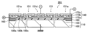
- FIG. 2 is a schematic cross-sectional view of the photoelectric conversion device according to the first embodiment of the semiconductor device of the present invention.
- FIG. 3 is a circuit configuration diagram of the photoelectric conversion device according to the first embodiment of the semiconductor device of the present invention. It is.
- the photoelectric conversion device 201 (solar cell module) of the present invention is formed on, for example, a grounded, substantially rectangular conductive substrate 100 made of a conductive material, and the conductive substrate 100.
- a support substrate 110 (a substrate made of a conductive material + a layer made of a non-conductive material) made of a non-conductive layer (insulating layer) 130 made of a non-conductive material, and a photoelectric substrate formed on the non-conductive layer 130. It has the electric power generation layer 140 which consists of the several photovoltaic cell 151 (photoelectric conversion element) of the converter 201.
- the power generation layer 140 is configured by arranging a plurality of solar cells 151 on a straight line and connecting two arrays connected in series in parallel. In FIG. 2, there are a total of two arrays connected in series on both sides of the central negative electrode, and the two arrays are connected in parallel.
- the photoelectric conversion device 201 of the present invention has a ribbon-shaped lead (not shown) with the positive electrode (plus) side of at least one solar cell 151a at both ends of the plurality of solar cells 151 of the power generation layer 140 as a positive electrode terminal. It is connected to a positive terminal of a contact box (not shown) through a wire, and is grounded by directly electrically connecting to the conductive substrate 100 of the support substrate 110 as a grounding terminal.
- the negative electrode (minus) side of one or two solar cells 151d at the center of the plurality of solar cells 151 is not shown as a negative electrode terminal via a ribbon-shaped lead wire (not shown). It is characterized in that it is connected to the negative terminal of the junction box.
- the conductive substrate 100 of the support substrate 110 is grounded, and its positive electrode is directly electrically connected to the conductive substrate 100 of the support substrate 110.
- the grounding solar cell 151a is grounded via the conductive layer 160, and the grounding solar cell 151a is most preferably a solar cell at both ends of the plurality of solar cells 151.
- the withstand voltage VW1 required with respect to the conductive substrate 100 is approximately the same as the withstand voltage Vw1d required from the potential difference V1d.
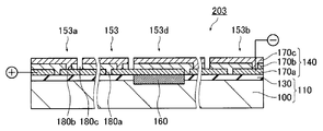
- the photoelectric conversion device 203 corresponds to the solar cell module 10 of Patent Document 1.
- the photoelectric conversion device 201 of the present embodiment When the number of photovoltaic cells in the photoelectric conversion device 201 of the present embodiment and the conventional photoelectric conversion device 203 are the same, the respective outputs are approximately the same. However, at the peripheral portion of the power generation layer where the required withstand voltage becomes high due to the influence of electric field concentration or creeping discharge, the photoelectric conversion device 201 of this embodiment has two sides at both end portions facing the substrate end of the solar cell 151d. Only the electric potential difference with the conductive substrate 100 becomes the maximum and the electric field concentrates, whereas the conventional photoelectric conversion device 203 has a conductive substrate extending over three sides facing the substrate end of the solar battery cell 153a or 153d.
- the photoelectric conversion device 201 of this embodiment is more advantageous for insulation.
- three sides face the substrate edge, and the other side faces the next cell. Yes.
- the solar cells 151 having the maximum potential difference from the conductive substrate 100 are at both ends of the plurality of solar cells 151 of the power generation layer 140. Since it is arrange
- the position of the grounding solar cell 151 a is at least one solar cell at both ends of the plurality of solar cells 151 of the power generation layer 140.
- the invention is not limited to this, and may be solar cells around both ends of the power generation layer 140. Furthermore, it is good also as at least 1 photovoltaic cell in the range of 10% of the number of the several photovoltaic cells 151 from the both ends of the electric power generation layer 140. The reason is that the solar cells 151 are connected in series from the solar cells 151d to at least one solar cell 151a at both ends among the plurality of solar cells 151 of one power generation layer 140.
- the number of solar cells 151 from the battery cell 151d to one solar cell around both ends is 40% or more of the total.
- the potential difference V1d is four times or more than the potential difference V1c between the solar cells around both ends of the power generation layer 140 and the conductive substrate 100. Therefore, in the photoelectric conversion device 201, the position of the grounding solar cell 151a is changed. This is because the potential difference V1d is the largest among all the solar battery cells 151 in the solar battery cells around both ends as in the case described above.
- the potential difference V1d is nine times Va1. That's it. For this reason, it is more preferable to set it as the at least 1 photovoltaic cell which exists in the range of 10% of the number of several photovoltaic cells 151 from both ends.
- the support substrate 110 used in the illustrated photoelectric conversion device 201 is a metal plate with an insulating layer having the conductive substrate 100 and the nonconductive layer 130 formed thereon.
- the supporting substrate 110 is not particularly limited as long as it is a metal plate with an insulating layer, but at least one surface side of an aluminum (Al) plate is anodized to make the anodized film a non-conductive layer 130. It is preferable that the support substrate 110 is obtained by using an Al plate that is formed and not anodized as the conductive substrate 100.
- the conductive substrate 100 is not particularly limited as long as the non-conductive layer 130 can be formed and the power generation layer 140 can be supported when the support substrate 110 is a metal plate with an insulating layer. Absent.
- the conductive substrate 100 is preferably an Al substrate having an Al layer on at least one surface. Examples thereof include an Al substrate and a composite Al substrate made of a composite material of Al and another metal.
- the thickness is preferably 0.05 to 10 mm.
- the support substrate 110 is manufactured from an Al substrate, a composite Al substrate, or the like, it is necessary to have a thickness that allows for a reduction in thickness due to anodic oxidation, pre-cleaning and polishing of the anodic oxidation.
- the Al substrate may be, for example, a Japanese Industrial Standard (JIS) 1000 series pure Al plate, or an Al alloy plate such as an Al—Mn alloy plate, an Al—Mg alloy plate, An alloy plate of Al and other metal elements such as an Al—Mn—Mg alloy plate, an Al—Zr alloy plate, an Al—Si alloy plate, and an Al—Mg—Si alloy plate may also be used.
- the composite Al substrate includes a clad plate of an Al plate and another metal plate, for example, a clad plate of a stainless steel (SUS) plate, and a clad plate in which various steel plates are sandwiched between two Al plates. Also good.
- the other metal plates constituting the clad plate with the Al plate are various stainless steel plates, for example, steel such as mild steel, 42 Invar alloy, Kovar alloy, or 36 Invar alloy.
- a metal plate that can be used as a roofing material or a wall material of a house or a building can be used so that the photoelectric conversion device of the present invention can be used as a roofing material integrated solar battery panel.
- the Al plate or Al alloy plate used here may contain various trace metal elements such as Fe, Si, Mn, Cu, Mg, Cr, Zn, Bi, Ni, and Ti.
- the nonconductive layer 130 formed on the conductive substrate 100 is not particularly limited.
- the conductive substrate 100 is an Al substrate or a composite Al substrate, it is preferably an anodized film formed on the surface of the Al substrate or the composite Al substrate by anodizing.
- the anodic oxidation of the Al substrate or the composite Al substrate can be performed by using the Al substrate or the composite Al substrate as an anode, immersing it in an electrolytic solution together with a cathode, and applying a voltage between the anode and the cathode to perform an electrolytic treatment.
- the anodic oxide film that becomes the non-conductive layer 130 may be formed on one surface of the Al layer of the Al substrate or the composite Al substrate that becomes the conductive substrate 100.
- the Al substrate or two Al plates may be used.
- the sandwiched clad plate in order to suppress warpage due to the difference in thermal expansion coefficient between the Al layer and the anodic oxide film, cracks generated in the anodic oxide film, etc. It is preferable to provide an anodic oxide film on the surface of the Al layer.
- the thickness of the non-conductive layer 130 thus formed that is, the thickness of the anodized film is not particularly limited.
- the non-conductive layer 130 only needs to have insulation and surface hardness that prevents damage due to mechanical shock during handling.
- the non-conductive layer 130 is too thick, there is a problem in terms of flexibility. There is a case. For this reason, the preferred thickness of the non-conductive layer 130 is 0.5 to 50 ⁇ m.
- the thickness of the non-conductive layer 130 can be controlled by electrolysis time together with constant current electrolysis or constant voltage electrolysis.
- various oxide layers such as glass containing elements such as Si, Ca, Zn, B, P, Ti, etc. in addition to the anodic oxide coating of Al are deposited, sol-gel method, etc. It may be formed by these various methods.
- the photoelectric conversion device 201 of the first embodiment of the present invention shown in FIG. 2 is called a substrate type, and the power generation layer 140 provided in the photoelectric conversion device 201 is of a thin film integrated type.
- the power generation layer 140 is disposed on the non-conductive layer 130 of the support substrate 110 in a straight line adjacent to the grounding solar cells 151a disposed at both ends of the power generation layer 140, and is connected in series. It has a plurality of solar cells 151 connected in parallel.
- the solar battery 151 includes a back electrode 170a formed on the surface of the non-conductive layer 130 of the support substrate 110 in FIG. 8 and a photoelectric conversion layer 170b formed on the back electrode 170a that converts received light into electricity. And a transparent electrode 170c formed on the photoelectric conversion layer 170b, and the back electrode 170a, the photoelectric conversion layer 170b, and the transparent electrode 170c are sequentially stacked on the non-conductive layer 130.
- the grounding solar cell 151a is a feature of the present invention, and a part of the non-conductive layer 130 formed on the support substrate 110 of the solar cell 151 is the conductive layer 160.
- the grounding solar cell 151a may be a cell that contributes to power generation as long as the conductive layer 160 that electrically connects and electrically connects the back electrode 170a and the conductive substrate 100 is formed. It may be a cell that does not contribute to.
- a buffer layer is formed on the photoelectric conversion layer 170b, and the back electrode 170a, the photoelectric conversion layer 170b, the buffer layer, and The transparent electrodes 170c may be sequentially stacked.
- the back electrode 170 a is applied from the region on the end side (a part on the right side in the drawing) of the adjacent (left side in the drawing) solar cell 151 or the grounding solar cell 151 a.
- the non-conductive layer 130 is formed by forming a P1 scribe groove 180a at a predetermined interval from the back surface electrode 170a of the adjacent solar battery cell 151 so as to be arranged in the most area of the solar battery cell 151 (left side in the figure). It is formed on the surface. Also in the grounding solar cell 151a, the back electrode 170a is formed from the region on the end side (a part on the right side in the drawing) of the adjacent (left side in the drawing) adjacent solar cell 151, as in the solar cell 151.
- the conductive layer 160 and the non-conductive layer are formed with a groove 180a at a predetermined interval from the back surface electrode 170a of the adjacent solar battery cell 151 so as to be arranged in the most area of the grounding solar battery cell 151a (left side in the figure). It is formed on the surface of the layer 130. Most of the back electrode 170 a of the grounding solar cell 151 a is disposed on the conductive layer 160.
- the photoelectric conversion layer 170b is formed on the back electrode 170a so as to fill the groove 180a between the adjacent back electrodes 170a. Therefore, the photoelectric conversion layer 170b is in direct contact with the non-conductive layer 130 and / or the conductive layer 160 at the portion of the groove 180a.
- the photoelectric conversion layer 170b is formed with a P2 scribe groove 180b extending from the adjacent solar cell 151 or the grounding solar cell 151a to the back electrode 170a extending. Therefore, the groove 180b is formed at a position (right side in the drawing) different from the groove 180a between the adjacent back surface electrodes 170a.
- the transparent electrode 170c is formed on the surface of the photoelectric conversion layer 170b so as to fill the groove 180b of the photoelectric conversion layer 170b. Therefore, the transparent electrode 170c is in direct contact with and electrically connected to the back surface electrode 170a of the adjacent solar cell 151 or the grounding solar cell 151a in the groove 180b. Thus, the two adjacent solar cells 151 and the adjacent solar cells 151 and the grounding solar cell 151a are connected in series.
- a groove 180c reaching the back electrode 170a is formed between the transparent electrode 170c and the photoelectric conversion layer 170b of the battery cell 151a.
- the adjacent two solar cells 151 and the adjacent solar cells 151 and the grounding solar cells 151a are separated by the groove 180c.
- the plurality of solar cells 151 and the grounding solar cell 151a are the solar cells 151 or the grounding solar cells 151a adjacent to the transparent electrode 170c of the solar cell 151 or the grounding solar cell 151a. Are connected in series by being connected to the back electrode 170a.
- the back electrodes 170a of the solar cells 151 at both ends are drawn out as positive terminals (+ terminals) by lead wires such as copper ribbons (not shown), and are centered or substantially omitted.
- the transparent electrode 170c of the central solar cell 151 is drawn out as a negative terminal ( ⁇ terminal) by a similar lead wire, and the back electrode 170a of the grounding solar cell 151a at both ends is connected via the grounding solar cell 151a. Then, it is grounded by being electrically connected to the grounded conductive substrate 100.
- the conductive substrate 100 is connected to the ground terminal by a similar lead wire.
- the solar cells 151 and the grounding solar cells 151a are parallel to one side of the rectangular conductive substrate 100 in a direction perpendicular to the cross section shown in FIG. 2 (a direction perpendicular to the paper surface of FIG. 2). It has a strip-like shape formed in an extending line shape. Accordingly, the back electrode 170 a and the transparent electrode 170 c are similarly strip-shaped electrodes that are long in one direction parallel to the side of the conductive substrate 100.
- the solar cell 151 of this embodiment is called an integrated CIGS solar cell (CIGS photoelectric conversion element).
- the back electrode 170a is a molybdenum electrode
- the photoelectric conversion layer 170b is CIGS
- the electrode 170c is made of ZnO.
- the buffer layer is formed, it is composed of CdS.
- the grounding solar battery 151a has the same configuration.
- such solar cells 151 and grounding solar cells 151a can be manufactured by, for example, a known CIGS solar cell manufacturing method. Further, in order to separate the groove 180a between the back electrode 170a, the groove 180b reaching the back electrode 170a formed in the photoelectric conversion layer 170b, the photoelectric conversion layer 170b, and the transparent electrode from the adjacent photoelectric conversion layer 170b and the transparent electrode. Line-shaped groove portions such as the groove 180c reaching the back electrode 170a can be formed by laser scribe or mechanical scribe.
- the photoelectric conversion device 201 of this embodiment when light is incident on the solar cell 151 and the grounding solar cell 151a from the transparent electrode 170c side, the light passes through the transparent electrode 170c and the buffer layer (not shown). When it passes through and reaches the photoelectric conversion layer 170b, an electromotive force is generated. For example, a current from the transparent electrode 170c toward the back electrode 170a is generated. Note that the arrows shown in FIG. 2 indicate the direction of current, and the direction of movement of electrons is opposite to the direction of current. Therefore, in FIG. 2, the back electrode 170a of the left end solar cell 151 is a positive electrode (+ electrode), and the transparent electrode 170c of the right end solar cell 151 is a negative electrode ( ⁇ electrode).
- the back electrode 170a and the transparent electrode 170c are for taking out the current generated in the photoelectric conversion layer 170b. Both the back electrode 170a and the transparent electrode 170c are made of a conductive material. The transparent electrode 170c on the light incident side needs to have translucency.
- the back electrode 170a is made of, for example, Mo, Cr, or W and a combination thereof.
- the back electrode 170a may have a single layer structure or a laminated structure such as a two-layer structure.
- the back electrode 170a preferably has a thickness of 100 nm or more, and more preferably 0.45 to 1.0 ⁇ m.
- the method for forming the back electrode 170a is not particularly limited, and can be formed by a vapor deposition method such as an electron beam evaporation method or a sputtering method.
- the transparent electrode 170c is made of, for example, ZnO, ITO (indium tin oxide), SnO 2 or a combination thereof.
- the transparent electrode 170c may have a single layer structure or a laminated structure such as a two-layer structure. Further, the thickness of the transparent electrode 170c is not particularly limited, and is preferably 0.3 to 1 ⁇ m.
- the method for forming the transparent electrode 170c is not particularly limited, and can be formed by a vapor deposition method such as an electron beam evaporation method or a sputtering method.
- An antireflection film such as MgF 2 may be formed on the transparent electrode 170c.
- the buffer layer is formed to protect the photoelectric conversion layer 170b when the transparent electrode 170c is formed and to transmit light incident on the transparent electrode 170c to the photoelectric conversion layer 170b.
- This buffer layer is made of, for example, CdS, ZnS, ZnO, ZnMgO, ZnS (O, OH), or a combination thereof.
- the buffer layer preferably has a thickness of 0.03 to 0.1 ⁇ m.
- the buffer layer is formed by, for example, a CBD (chemical bath) method, a solution growth method, or the like. Note that a high resistance film made of ZnO or the like may be formed between the buffer layer such as CBD-CdS and the transparent electrode 170c such as ZnO: Al.
- the photoelectric conversion layer 170b is a layer that generates current by absorbing light that has passed through the transparent electrode 170c and the buffer layer.
- the configuration of the photoelectric conversion layer 170b is not particularly limited, and is preferably, for example, at least one compound semiconductor having a chalcopyrite structure.
- the photoelectric conversion layer 170b may be at least one compound semiconductor composed of a group Ib element, a group IIIb element, and a group VIb element.
- the photoelectric conversion layer 170b includes at least one type Ib group element selected from the group consisting of Cu and Ag, and a group consisting of Al, Ga, and In.
- this compound semiconductor CuAlS 2 , CuGaS 2 , CuInS 2 , CuAlSe 2 , CuGaSe 2 , CuInSe 2 (CIS), AgAlS 2 , AgGaS 2 , AgInS 2 , AgAlSe 2 , AgGaSe 2 , AgInSe 2 , AgInSe 2 , AgInSe 2 , AgInSe 2 , AgInSe 2 , AgInT , AgInTe 2 , Cu (In 1-x Ga x ) Se 2 (CIGS), Cu (In 1-x Al x ) Se 2 , Cu (In 1-x Ga x ) (S, Se) 2 , Ag (In 1-x Gax) Se 2 , Ag (In 1-x Ga x ) (S, Se) 2 and
- the photoelectric conversion layer 170b particularly preferably includes CuInSe 2 (CIS) and / or Cu (In, Ga) Se 2 (CIGS) in which Ga is dissolved.
- CIS and CIGS are semiconductors having a chalcopyrite crystal structure, have high light absorption, and high photoelectric conversion efficiency has been reported. Moreover, there is little degradation of efficiency by light irradiation etc. and it is excellent in durability.
- the photoelectric conversion layer 170b contains impurities for obtaining a desired semiconductor conductivity type. Impurities can be contained in the photoelectric conversion layer 170b by diffusion from adjacent layers and / or active doping.
- the constituent elements and / or impurities of the I-III-VI group semiconductor may have a concentration distribution, and a plurality of layer regions having different semiconductor properties such as n-type, p-type, and i-type May be included.
- the band gap width / carrier mobility and the like can be controlled, and the photoelectric conversion efficiency can be designed high.
- the photoelectric conversion layer 170b may contain one or more semiconductors other than the group I-III-VI semiconductor.
- semiconductors other than I-III-VI group semiconductors include semiconductors composed of group IVb elements such as Si (group IV semiconductors), semiconductors composed of group IIIb elements such as GaAs and group Vb elements (group III-V semiconductors), and Examples thereof include semiconductors composed of IIb group elements such as CdTe and VIb group elements (II-VI group semiconductors).
- the photoelectric conversion layer 170b may contain an arbitrary component other than a semiconductor and impurities for obtaining a desired conductivity type as long as the characteristics are not hindered.
- the content of the I-III-VI group semiconductor in the photoelectric conversion layer 170b is not particularly limited.
- the content of the group I-III-VI semiconductor in the photoelectric conversion layer 170b is preferably 75% by mass or more, more preferably 95% by mass or more, and particularly preferably 99% by mass or more.
- the CIGS layer may be formed by 1) a multi-source co-evaporation method, 2) a selenization method (selenization / sulfurization method), or 3) a sputtering method. 4) a hybrid sputtering method, and 5) a mechanochemical process method are known.
- the selenization method is also called a two-step method.
- a metal precursor of a laminated film such as a Cu layer / In layer or a (Cu—Ga) layer / In layer is sputtered, vapor deposited, or electrodeposited.
- a selenium compound such as Cu (In 1-x Ga x ) Se 2 is produced by a thermal diffusion reaction by heating the film to 450 to 550 ° C. in selenium vapor or hydrogen selenide. is there.
- This method is called a vapor phase selenization method.
- there is a solid-phase selenization method in which solid-phase selenium is deposited on a metal precursor film and selenized by a solid-phase diffusion reaction using the solid-phase selenium as a selenium source.
- a Cu—Ga alloy film is first deposited, an In film is deposited thereon, and when this is selenized, natural thermal diffusion is used to form Ga.
- a method of inclining the concentration in the film thickness direction K. Kushiya et.al, Tech.Digest 9th Photovoltaic Science and Engineering Conf.Miyazaki, 1996 (Intn.
- a sputtering method As a sputtering method, a method using CuInSe 2 polycrystal as a target, a two-source sputtering method using Cu 2 Se and In 2 Se 3 as a target and using a H 2 Se / Ar mixed gas as a sputtering gas (J. Ermer, et.al, Proc. 18th IEEE Photospecifics Conf. (1985) 1655-1658., Etc.), and a three-source sputtering method in which a Cu target, an In target, and a Se or CuSe target are sputtered in Ar gas (T Nakada, et.al, Jpn.J.Appl.Phys.32 (1993) L1169-L1172, etc.).
- CIGS film formation methods include screen printing, proximity sublimation, MOCVD, and spraying.
- a fine particle film containing an Ib group element, an IIIb group element, and a VIb group element is formed on a substrate by a screen printing method or a spray method, etc.
- Japanese Patent Laid-Open No. 9-74065 and Japanese Patent Laid-Open No. 9-74213 are examples of Japanese Patent Laid-Open No. 9-74065 and Japanese Patent Laid-Open No. 9-74213).
- the solar cells 151 and the grounding solar cells 151a of the photoelectric conversion device 201 (solar cell module) of the first embodiment described above are integrated CIGS solar cells, but the present invention is limited to this.
- the configuration of the solar cell and the photoelectric conversion element, particularly the photoelectric conversion layer, functioning as the solar cell of the photoelectric conversion device (solar cell module) of the present invention is, for example, an amorphous silicon (a-Si) solar cell Cell, tandem solar cell (a-Si / a-SiGe tandem solar cell), series connection (SCAF) solar cell (a-Si serial connection solar cell), CdTe (cadmium tellurium) )
- Solar cell III-V solar cell, thin-film silicon solar cell, dye-sensitized solar cell, or organic solar cell It may be me, even what is referred to as a substrate type, may be what is called a super straight type.
- the back electrode 170a side is the positive electrode (+ electrode) and the transparent electrode 170c side is the negative electrode ( ⁇ electrode).
- the present invention is not limited to this, and the solar cell Depending on the cell, the back electrode 170a side may be the negative electrode ( ⁇ electrode) and the transparent electrode 170c side may be the positive electrode (+ electrode).
- a tandem solar cell (a-Si / a-SiGe tandem solar cell) is used as the solar cell 151 and the grounding solar cell 151a, for example, Ag
- the transparent electrode 170c is made of ITO
- the photoelectric conversion layer 170b is made of an intrinsic semiconductor layer such as an n-type semiconductor layer, microcrystalline silicon, and amorphous silicon germanium (a-SiGe).
- a p-type semiconductor layer is stacked, and an n-type semiconductor layer, an intrinsic semiconductor layer such as amorphous silicon (a-Si), and a photoelectric conversion layer on which a p-type semiconductor layer is stacked can be used.
- a photoelectric conversion layer called a CdTe (cadmium tellurium) type is used as the photoelectric conversion layer 170b. it can.
- the conductive layer 160 of the grounding solar cell 151a will be described.
- the conductive layer 160 is the most characteristic part of the present invention, and is disposed in place of the nonconductive layer 130 between the conductive substrate 100 and the back electrode 170a in the grounding solar cell 151a.
- the back electrode 170a having conductivity is electrically connected to the grounded conductive substrate 100 to be conductive and grounded.
- the conductive layer 160 is a mixture of the component of the conductive substrate 100, the component of the non-conductive layer 130, and the component of the back electrode 170a. As a result, the conductive layer 160 has conductivity. .
- the conductive layer 160 is formed only on the lower portion of the back electrode 170a of the grounding solar cell 151a, and is not formed on the lower portion of the groove 180a and is nonconductive.
- the present invention is not limited to this, and the lower portion of the groove 180a and the lower portion of the back electrode 170a of the adjacent solar cell 151 are provided in the grounding solar cell 151a.
- the conductive layer 160 may be used. However, in this case, since the back electrode 170a of the grounding solar cell 151a and the back electrode 170a of the adjacent solar cell 151 are short-circuited, the grounding solar cell 151a does not contribute to power generation.
- such a conductive layer 160 is obtained by applying ultrasonic solder 190 on the transparent electrode 170 c of the solar battery cell 151 to be the grounding solar battery cell 151 a and applying the ultrasonic solder 190.
- the nonconductive layer 130 corresponding to the portion where the ultrasonic solder 190 of the solar cell 151a is applied is destroyed and the nonconductive material is destroyed.
- the surfaces of the conductive substrate 100 and the back electrode 170a that have been in contact with the layer 130 are dissolved and mixed, and the conductive substrate 100, the back electrode 170a, and the broken non-conductive layer 130 are mixed to form. be able to.
- the formation of the mixed state of the conductive layer 14 is not particularly clarified, for example, only the solar battery cell 151a to which the ultrasonic solder 190 is applied is subjected to the heating ultrasonic treatment, whereby the solar battery cell 151a.
- the non-conductive layer 130 corresponding to the portion to which the ultrasonic solder 190 is applied is broken to create a fine void to be porous, and the conductive substrate that is in contact with the broken non-conductive layer 130 It is presumed that a mixed state is formed by entering the fine voids of the non-conductive layer 130 that is broken by melting the surfaces of the 100 and the back electrode 170a.
- the conductive layer 160 mixed with these and the ultrasonic solder 190 may be formed.
- the solder may be applied to the entire surface of the grounding solar cell 151a, but the transparent electrode 170c may be left partly as shown in FIG.
- soldering may be performed in a linear manner while supplying solder onto the cell without applying solder, but soldering may be performed on the wire at a time after placing the solder, or a plurality of linear locations may be provided. Soldering at the same time is preferable for production.
- the conductivity of the conductive layer 160 formed in this way is considered to be determined by the mixed state of the conductive layer 160. Therefore, the configuration or function of the solar cell 151 to be the grounding solar cell 151a and Depending on the necessity of the power generation function, especially the thickness of the non-conductive layer 130, etc., the amount of ultrasonic solder 190 applied, the heating temperature, the heating time, the ultrasonic strength and the ultrasonic processing time, etc. Can be controlled by appropriately controlling the required electric conductivity.
- the conductivity of the conductive layer 160, the configuration and function of the solar cell 151, particularly the thickness of the non-conductive layer 130, the coating amount of the ultrasonic solder 190, the heating temperature in the heating ultrasonic treatment, the heating time, the ultrasonic wave The relationship between the strength and the sonication time may be obtained in advance by experiments or simulations.
- the conductive layer 160 is formed as described above. However, the present invention is not limited to this, and if the non-conductive layer 130 is formed on the substrate 101 made of a conductive material, You may form in any step of manufacture of a photoelectric conversion apparatus.
- the non-conductive layer 130 on the conductive substrate 100 is coated with ultrasonic solder on a corresponding portion to be the grounding solar cell 151a and subjected to heating ultrasonic treatment, and the broken non-conductive layer 130 and A conductive layer 160 in which the conductive substrate 100 and ultrasonic solder are mixed may be formed, and then a plurality of solar cells 151 and grounding solar cells 151a may be formed.
- ultrasonic solder is applied to the back electrode 170a corresponding to the ground solar cell 151a, and heating ultrasonic treatment is performed.
- the conductive layer 160 in which the broken non-conductive layer 130, the conductive substrate 100, and the back electrode 170a are mixed, or the conductive layer 160 in which ultrasonic solder is also mixed is formed, and sequentially,
- the photoelectric conversion layer 170b and the transparent electrode 170c may be formed to form a plurality of solar cells 151 and grounding solar cells 151a. Further, after forming the photoelectric conversion layer 170b, the conductive layer 160 is formed in the same manner, and the transparent electrode 170c is formed thereon to form a plurality of solar cells 151 and grounding solar cells 151a. May be.
- the solar battery cell 151 since the solar battery cell 151 is completed after forming the conductive layer 160, it is necessary to form one or more of the back electrode 170a, the photoelectric conversion layer 170b, and the transparent electrode 170c. Therefore, since accurate alignment is required, it is preferable to form the conductive layer 160 after forming the solar cells 151.
- FIG. 5 is a flowchart showing an example of a method of manufacturing the photoelectric conversion device according to the first embodiment of the present invention shown in FIG.
- the anodic oxidation treatment is performed by the above-described method to form an anodic oxide film that becomes the non-conductive layer 130 on the surface, thereby having the anodic oxide film.
- An Al substrate is formed and prepared as a support substrate 110 (step S100).
- an Al substrate having an anodized film may be prepared in advance as the support substrate 110.
- Mo is deposited on the non-conductive layer 130 of the support substrate 110 by a known film formation method such as the DC magnetron sputtering method described above to form a Mo film (step S102).
- the Mo film thus formed on the non-conductive layer 130 is cut by the laser scribing method described above, and is patterned into the pattern 1 to form the groove 180a, thereby forming the back electrode 170a (step S104).
- the photoelectric conversion layer 170b and the photoelectric conversion layer 170b are formed by a known method such as the above-described selenization / sulfurization method or multi-source co-evaporation method so as to fill the groove 180a on the back electrode 170a formed on the non-conductive layer 130.
- a CIGS compound semiconductor film (p-type CIGS light absorption film) is formed (step S106). Subsequently, a CdS film (n-type high resistance buffer layer) to be a buffer layer is formed on the CIGS compound semiconductor film thus formed by a known method such as CBD described above (step S108).
- the CIGS compound semiconductor film and the CdS film thus formed on the back electrode 170a are integrally cut by the mechanical scribing method described above, and patterned into the pattern 2 to form the groove 180b reaching the back electrode 170a. Then, the photoelectric conversion layer 170b and the buffer layer are formed (step S110).
- a ZnO film (n-type ZnO) that becomes the transparent electrode 170c by a known method such as the above-described MOCVD method or RF sputtering method so as to fill the groove 180b on the buffer layer (photoelectric conversion layer 170b) thus formed.
- a transparent conductive film window layer is formed (step S112).
- the ZnO film, the buffer layer, and the photoelectric conversion layer 170b thus formed are integrated, cut by the mechanical scribing method described above, and patterned into the pattern 3, and between the adjacent solar cells 151, the back electrode 170a.
- the solar cell 151 is separated into the photoelectric conversion layer 170b, the buffer layer, and the transparent electrode 170c to form a plurality of solar cells 151 (step S114).
- the ultrasonic solder 190 is applied on the transparent electrode 170c of the solar battery cell 151 to be the preset grounding solar battery cell 151a (step S116).
- the transparent electrode 170c of the solar battery cell 151 to which the ultrasonic solder 190 is applied is selectively subjected to heating ultrasonic treatment, and the non-conductive layer 130 is broken to remove the component and the component of the conductive substrate 100.
- the conductive layer 160 is formed by mixing the components of the back electrode 170a (step S118).
- the photoelectric conversion device 201 of the present embodiment is formed (step S118).
- FIG. 6 is a schematic cross-sectional view of the photoelectric conversion device 202 (solar cell module) of the second embodiment of the semiconductor device of the present invention.
- the photoelectric conversion apparatus 202 of this embodiment shown in FIG. 6 and the photoelectric conversion apparatus 201 of 1st Embodiment shown in FIG. 1 differ except the structure of the conductive layer 160 of the photovoltaic cell 151a for grounding.
- the same components are denoted by the same reference numerals, and detailed description thereof is omitted.
- the photoelectric conversion device 202 of this embodiment extends from an adjacent solar cell 151 instead of the conductive layer 160 of the grounding solar cell 151 a of the photoelectric conversion device 201 of the first embodiment.
- the existing back electrode 170a is directly disposed between the conductive substrate 100 and the photoelectric conversion layer 170b to form the conductive layer 160. Therefore, in the photoelectric conversion device 202 of the present embodiment, the back electrode 170a and the grounded conductive substrate 100 are in direct contact and are electrically connected, so that the back electrode 170a of the grounding solar cell 151a is electrically conductive. It can be grounded through the conductive substrate 100.
- the solar cell 151 and the grounding solar cell 151a have any configuration. Of course, it may be (photoelectric conversion element, photoelectric conversion layer).
- the non-conductive layer 130 such as the anodic oxide film is not formed only in the portion corresponding to the grounding solar cell 151a, and the anodic oxide film is formed in the other portions.
- the power generation layer 140 is formed using the support substrate 110 made of the conductive substrate 100 such as an Al substrate on which the non-conductive layer 130 such as is formed. That is, the back electrode 170a and the conductive layer 160, the photoelectric conversion layer 170b and the buffer layer, and the transparent electrode 170c are sequentially formed, and a plurality of solar cells 151 and a grounding solar cell 151a are formed. be able to.
- the photoelectric conversion device 202 of this embodiment can be formed.
- the entire surface of the conductive substrate 100 such as an anodized Al substrate is used instead of the support substrate 110 made of the conductive substrate 100 in which the nonconductive layer 130 is not formed only on the portion corresponding to the grounding solar cell 151a.
- the support substrate 110 in a state where the nonconductive layer 130 such as the anodized film corresponding to the ground solar cell 151a of the support substrate 110 on which the nonconductive layer 130 is formed is removed by scribing or etching is used.
- the photovoltaic layer 202 of this embodiment may be formed by forming the power generation layer 140 starting from the deposition of the back electrode 170a.
- both the photoelectric conversion device 201 (solar cell module) of the first embodiment and the photoelectric conversion device 202 (solar cell module) of the second embodiment may include a conductive frame.
- this conductive frame in order to place the solar cell module on a roof base material such as a base plate or a waterproof underlaying material, the peripheral edge of the solar cell module, that is, the ridge side, the eaves side, the left side, It is a member for a solar cell module attached to the right edge.
- the conductive frame an aluminum frame suitable for workability and environmental resistance is mainly used.
- both the photoelectric conversion device 201 (solar cell module) of the first embodiment and the photoelectric conversion device 202 (solar cell module) of the second embodiment may be connected in series to form a solar cell string. Furthermore, it is good also as a solar cell array by connecting this solar cell string in parallel.
- the photoelectric conversion device 201 of the first embodiment the photoelectric conversion device 202 of the second embodiment, the conventional photoelectric conversion device 203, and the solar cell described in FIG. Compare modules 50.
- a photoelectric conversion device capable of outputting 100 W can be obtained.
- the photoelectric conversion device 201 according to the first embodiment, the photoelectric conversion device 202 according to the second embodiment, the conventional photoelectric conversion device 203, and the solar described in FIG. 7 of Patent Document 1 as a general photoelectric conversion device.
- the ends X11 and X12 of one or two solar cells at the center of the plurality of solar cells, the ends of two solar cells at both ends of the plurality of solar cells Part X21, X22, X23, X24, potential difference VX11, VX12, VX21 between the solar battery cell and the conductive substrate at each point of the central part X31, X32 of the two solar battery cells at both ends of the plurality of solar battery cells VX22, VX23, VX24, VX31, and VX32 are shown in Table 1 below.
- the photoelectric converter 201 has a small potential difference between each solar cell and the conductive substrate. Therefore, since the withstand voltage VW required between the power generation layer and the conductive substrate can be reduced, the insulation withstand voltage can be improved.
- the grounding solar cells 151a are arranged around both ends of the power generation layer 140 in the photoelectric conversion devices 201 according to the first and second embodiments.
- the remaining solar cells 151 are arranged in a straight line adjacent to this, and two arrays connected in series are connected in parallel, so that the solar cell 151d is included in all the solar cells 151.
- the solar cell 151 has the largest potential difference V1d with respect to the conductive substrate 100. Therefore, since the withstand voltage VW is reduced, the insulation is improved and the insulation withstand voltage is excellent.
- the present invention is basically configured as described above. As described above, the photoelectric conversion device has been described in detail as an example of the semiconductor device of the present invention. However, the present invention is not limited to the above-described embodiment, and various improvements or modifications can be made without departing from the gist of the present invention. Of course it is also good.
Abstract
This semiconductor device has a conductive substrate formed from a conductive material, a nonconductive layer provided on at least part of the surface of the conductive substrate, a plurality of semiconductor elements provided on this nonconductive layer, wiring that electrically connects the plurality of semiconductor elements, and at least one electrical connection part between the nonconductive layer and semiconductor elements or wiring. The semiconductor element for which the potential difference with the conductive substrate is the greatest is disposed in a position other than the geometric terminal of the arrangement created by the plurality of semiconductor elements.
Description
本発明は、半導体装置、太陽電池モジュール、太陽電池ストリング及び太陽電池アレイに関し、特に、半導体装置において、導電性材料からなる導電性基板と半導体素子との間の絶縁性を向上させた半導体素子の配置方法、ならびにこの半導体素子を用いた、太陽電池モジュール、太陽電池ストリング及び太陽電池アレイに関する。
The present invention relates to a semiconductor device, a solar cell module, a solar cell string, and a solar cell array, and more particularly, in a semiconductor device, a semiconductor element having improved insulation between a conductive substrate made of a conductive material and a semiconductor element. The present invention relates to an arrangement method and a solar cell module, a solar cell string, and a solar cell array using the semiconductor element.
軽量性、可撓性という特徴を持った金属、合金等の導電性材料からなる基板は、広い用途に適用できる可能性がある。さらに、上記導電性材料からなる基板は高温プロセスにも耐え得るため、ポリイミド等の樹脂基板では扱うことのできない半導体にも適用することができる。例えば、太陽電池用基板として用いれば光電変換効率を向上させることができ、太陽電池の高効率化が期待できる。
A substrate made of a conductive material such as a metal or alloy having the characteristics of lightness and flexibility may be applicable to a wide range of applications. Further, since the substrate made of the conductive material can withstand high temperature processes, it can be applied to a semiconductor that cannot be handled by a resin substrate such as polyimide. For example, if it is used as a substrate for a solar cell, the photoelectric conversion efficiency can be improved, and high efficiency of the solar cell can be expected.
しかし、金属、合金等の導電性材料を基板として使用する場合、基板上に形成される半導体素子及び配線と基板との間に絶縁層を設け、各部の電位差が調整されている必要がある。通常は、導電性材料からなる基板の少なくとも片面に絶縁層を設ける。
絶縁層としては、基板材料を陽極酸化した酸化物等が用いられる(例えば、特許文献1)。 However, when a conductive material such as a metal or an alloy is used as the substrate, it is necessary to provide an insulating layer between the semiconductor element and wiring formed on the substrate and the substrate, and to adjust the potential difference of each part. Usually, an insulating layer is provided on at least one surface of a substrate made of a conductive material.
As the insulating layer, an oxide obtained by anodizing a substrate material is used (for example, Patent Document 1).
絶縁層の絶縁性を向上させる方法として、特許文献1には、直列接続した素子(すなわち太陽電池セル)の中間付近の電位と導電性材料からなる基板(金属基板)の電位を等電位にすることによって、素子と基板との電位差を小さくすることが開示されている。
As a method for improving the insulation of the insulating layer, Patent Document 1 discloses that the potential in the vicinity of the middle of series-connected elements (that is, solar cells) and the potential of the substrate made of a conductive material (metal substrate) are made equipotential. Accordingly, it is disclosed that the potential difference between the element and the substrate is reduced.
しかしながら、特許文献1において、半導体素子によって作られる配列の末端部(両端部)では基板との電位差が最大となり、沿面放電又は角部での電界集中等によって、絶縁性が低下するという問題があった。
図7(a)、(b)に電極角部での電解集中の様子をシミュレーションした結果を示す。図7(a)は角部の曲率を変化させた場合の結果を示し、図7(b)は角部の角度を変化させた場合の結果を示す。
図7(a)から直径25mmの電極端部(曲率半径12.5mmの電極角部に対応する)での電界Emaxが電極中央部の電界E0の1.3倍程度となることがわかり、図7(b)では角部が直角での電界Emaxが電極中央部の電界E0の1.1倍程度となることがわかる。
角部での電界集中を抑えるために、例えば、特許文献2では角部を丸くすることが開示されており、特許文献3では角部を鈍角にすることが開示されている。しかし、依然として末端部では基板との電位差が最大であるために、末端部では絶縁性が低いという問題があった。 However, in Patent Document 1, there is a problem that the potential difference from the substrate is maximized at the end portion (both ends) of the array formed by the semiconductor element, and insulation is deteriorated due to creeping discharge or electric field concentration at the corner portion. It was.
FIGS. 7A and 7B show the results of simulating the state of electrolytic concentration at the electrode corners. FIG. 7A shows the result when the curvature of the corner is changed, and FIG. 7B shows the result when the angle of the corner is changed.
From FIG. 7A, it can be seen that the electric field E max at the electrode end portion having a diameter of 25 mm (corresponding to the electrode corner portion having a curvature radius of 12.5 mm) is about 1.3 times the electric field E 0 at the center portion of the electrode. In FIG. 7B, it can be seen that the electric field E max at a right corner is about 1.1 times the electric field E 0 at the center of the electrode.
In order to suppress the electric field concentration at the corner, for example, Patent Document 2 discloses rounding the corner, and Patent Document 3 discloses making the corner an obtuse angle. However, since the potential difference from the substrate is still the maximum at the end portion, there is a problem that the insulating property is low at the end portion.
また、特許文献4には、基板上の配線間の電位差の平面分布を小さくするという課題に対して、配線配置を工夫することが開示されている。
しかし、特許文献4に開示されている方法は、基板が導電性材料からなる場合に、半導体素子及び配線と基板との電位を調整する方法が開示されていないため、この方法をそのまま適用しても基板との絶縁性を向上させることはできない。 Further, Patent Document 4 discloses that a wiring arrangement is devised for the problem of reducing the planar distribution of a potential difference between wirings on a substrate.
However, since the method disclosed in Patent Document 4 does not disclose a method for adjusting the potential between the semiconductor element and the wiring and the substrate when the substrate is made of a conductive material, the method is applied as it is. However, the insulation with the substrate cannot be improved.
本発明の目的は、前記従来技術に基づく問題点を解消し、導電性材料からなる導電性基板上に設けられる複数の半導体素子と導電性基板との間の絶縁耐電圧性が優れた半導体装置、太陽電池モジュール、太陽電池ストリング及び太陽電池アレイを提供することを目的とする。
SUMMARY OF THE INVENTION An object of the present invention is to eliminate the problems based on the prior art and to provide a semiconductor device with excellent insulation withstand voltage between a plurality of semiconductor elements provided on a conductive substrate made of a conductive material and the conductive substrate. It aims at providing a solar cell module, a solar cell string, and a solar cell array.
上記目的を達成するために、本発明の第1の態様は、導電性材料からなる導電性基板と、基板の表面の少なくとも一部に設けられた非導電性材料からなる非導電性層と、非導電性層上に設けられる複数の半導体素子と、複数の半導体素子を電気的に接続する配線と、導電性基板と、半導体素子又は配線とを接続する少なくとも1つの電気的接続部とを有し、導電性基板との電位差が最大となる半導体素子は、複数の半導体素子によって作られる配列の幾何学的な末端を除く位置に配置されていることを特徴とする。
In order to achieve the above object, a first aspect of the present invention includes a conductive substrate made of a conductive material, a nonconductive layer made of a nonconductive material provided on at least a part of the surface of the substrate, A plurality of semiconductor elements provided on the non-conductive layer; wiring that electrically connects the semiconductor elements; a conductive substrate; and at least one electrical connection portion that connects the semiconductor element or the wiring. The semiconductor element having the maximum potential difference from the conductive substrate is arranged at a position excluding a geometric end of an array formed by a plurality of semiconductor elements.
本発明において、幾何学的な末端とは、例えば、複数の半導体素子によって作られる配列が一線分の場合は、図1(a)に示すように、複数の半導体素子51のうち、線分の頂点を含む半導体素子51aを指す。また、幾何学的な末端とは、図1(b)に示すように、複数の半導体素子51によって作られる配列が多角形の場合は、多角形の頂点を含む半導体素子51aを指す。また、幾何学的な末端とは、図1(c)に示すように、半導体素子51の形が多角形の場合は、その頂点を含む半導体素子51aを指し、図1(d)に示すように、複数の半導体素子51の配列が同心円状の場合、円周を含む半導体素子51aを指す。1つの半導体素子の形がどのような形であれ、本発明では、上述のいずれかを含む半導体素子51aを幾何学的な末端とする。
In the present invention, the geometric end means, for example, when an array formed by a plurality of semiconductor elements is one line segment, as shown in FIG. The semiconductor element 51a including the apex is indicated. In addition, as shown in FIG. 1B, the geometric end indicates a semiconductor element 51a including a vertex of a polygon when the array formed by the plurality of semiconductor elements 51 is a polygon. In addition, as shown in FIG. 1C, the geometric end refers to the semiconductor element 51a including the vertex when the shape of the semiconductor element 51 is a polygon, as shown in FIG. 1D. In addition, when the arrangement of the plurality of semiconductor elements 51 is concentric, the semiconductor element 51a including the circumference is indicated. Regardless of the shape of one semiconductor element, in the present invention, the semiconductor element 51a including any of the above-described elements is defined as a geometric end.
また、本発明においては、電気的接続部とは、例えば、半導体素子の一部に圧力をかけて押し付けるような機械的接触部、半田付け等の合金的接合部、該当箇所を加熱溶融してなる溶接部等が含まれる。また、基板と半導体素子が接触していなくても、例えば、薄い絶縁層があること、及び半導体的性質を持っているものがあること等のように、実質的に基板に対する半導体素子の電位を決定できる部分も電気的接続部に含まれる。
電気的接続部によって、導電性基板(導電性材料部分)と半導体素子との電位差が調整される。
配線によって各半導体素子が直列又は並列に接続されることによって、導電性基板と、半導体素子又は配線との間の電位差分布が調整される。 In the present invention, the electrical connection portion is, for example, a mechanical contact portion that presses against a part of a semiconductor element to press it, an alloyed joint portion such as soldering, and the corresponding portion is heated and melted. Welding parts and the like. Further, even if the substrate and the semiconductor element are not in contact with each other, the potential of the semiconductor element with respect to the substrate is substantially reduced, for example, there is a thin insulating layer and there is a semiconductor property. The part that can be determined is also included in the electrical connection.
The potential difference between the conductive substrate (conductive material portion) and the semiconductor element is adjusted by the electrical connection portion.
Each semiconductor element is connected in series or in parallel by wiring, whereby the potential difference distribution between the conductive substrate and the semiconductor element or wiring is adjusted.
導電性基板(導電性材料部分)との間の電位差が最大となる半導体素子を、配列の幾何学的な末端を除く位置に配置することによって、末端部分での電界が緩和される。
末端部分での電界が緩和されることによって、導電性基板(導電性材料部分)と半導体素子との間の絶縁耐電圧性が向上する。
また、電気的接続部と接する半導体素子は、好ましくは配列の少なくとも1つの末端から複数の半導体素子の数の10%の範囲に配置され、より好ましくは配列の少なくとも1つの末端から複数の半導体素子の数の5%の範囲に配置され、互いに等電位となる少なくとも1つの半導体素子であることを特徴とする。特に好ましくは配列の少なくとも1つの末端に配置される半導体素子であることを特徴とする。
配列の末端付近が導電性材料部分と等電位となることにより、末端部での電位差を小さくすることができる。
末端部周辺における電位差が小さくなることによって、電界集中が緩和され全体の絶縁性が高まる。 By arranging the semiconductor element having the maximum potential difference with respect to the conductive substrate (conductive material portion) at a position excluding the geometric end of the array, the electric field at the end portion is reduced.
By reducing the electric field at the terminal portion, the insulation withstand voltage between the conductive substrate (conductive material portion) and the semiconductor element is improved.
Further, the semiconductor element in contact with the electrical connection portion is preferably arranged in a range of 10% of the number of the plurality of semiconductor elements from at least one end of the array, and more preferably, the plurality of semiconductor elements from at least one end of the array It is characterized in that it is at least one semiconductor element which is arranged in the range of 5% of the number of and which are equipotential to each other. The semiconductor element is particularly preferably a semiconductor element disposed at at least one end of the array.
Since the vicinity of the end of the array is equipotential with the conductive material portion, the potential difference at the end can be reduced.
By reducing the potential difference around the end portion, the electric field concentration is alleviated and the overall insulation is enhanced.
また、本発明の別態様の半導体装置において、非導電性層は、導電性基板を陽極酸化処理することにより形成されたものであり、複数の半導体素子のうち、最大電位となる少なくとも1つの半導体素子は電気的接続部と接していることを特徴とする。
陽極酸化膜は、母体金属側を正極とした場合の方が絶縁性は高くなることが知られている。最大電位となる半導体素子と導電性基板(導電性材料部分)が等電位となることにより、常に導電性基板(導電性材料部分)が正極となるため、全体の絶縁性が高まる。
導電性基板としては、軽量性、可撓性があるチタン又はアルミニウムからなる基板が好ましく、安価なアルミニウムからなる基板がより好ましい。また、諸特性を向上させるために、アルミニウムからなる基板ではなく、複合材料からなる複合アルミニウム基板が好ましい。複合材料には、例えば、樹脂又は他金属とアルミニウムとを合わせた材料等が含まれる。中でも鋼板又はステンレス板とアルミニウム板とのクラッド基板は、アルミニウムの耐熱性を向上できるため、より好ましい。 In the semiconductor device according to another aspect of the present invention, the nonconductive layer is formed by anodizing a conductive substrate, and at least one semiconductor having a maximum potential among a plurality of semiconductor elements. The element is in contact with the electrical connection.
It is known that the anodic oxide film has higher insulating properties when the base metal side is the positive electrode. When the semiconductor element having the maximum potential and the conductive substrate (conductive material portion) are equipotential, the conductive substrate (conductive material portion) is always the positive electrode, so that the overall insulation is improved.
As the conductive substrate, a lightweight and flexible substrate made of titanium or aluminum is preferable, and an inexpensive substrate made of aluminum is more preferable. In order to improve various characteristics, a composite aluminum substrate made of a composite material is preferable instead of a substrate made of aluminum. The composite material includes, for example, a material in which a resin or another metal is combined with aluminum. Among them, a clad substrate made of a steel plate or a stainless steel plate and an aluminum plate is more preferable because it can improve the heat resistance of aluminum.
また、本発明の別態様の半導体装置は、複数の半導体素子は、同心円状に配置されており、導電性基板との電位差が最大となる少なくとも1つの半導体素子は、同心円状の配置の中心に配置されることを特徴とする。
同心円状の配列によって電界集中が緩和され、導電性基板との電位差が最大となる少なくとも1つの半導体素子と導電性基板との電位差が配列の末端から最も離れた位置にあるために、導電性基板に平行な方向の電界が小さくなり、全体の絶縁性が向上する。 In the semiconductor device according to another aspect of the present invention, the plurality of semiconductor elements are concentrically arranged, and at least one semiconductor element having the maximum potential difference from the conductive substrate is disposed at the center of the concentric arrangement. It is characterized by being arranged.
The electric field concentration is mitigated by the concentric arrangement, and the potential difference between the conductive substrate and at least one semiconductor element that maximizes the potential difference with the conductive substrate is located farthest from the end of the arrangement. Thus, the electric field in the direction parallel to is reduced, and the overall insulation is improved.
また、本発明の別態様の半導体装置は、複数の半導体素子が一直線上に配置され、直列接続される2つの配列が並列に接続されることを特徴とする。全ての半導体素子が一直線上に配置されることによって製造プロセスを増やすことがなく、かつ2つの直列回路が並列に接続されることによって出力電圧が半分になるため要求される耐電圧を半分にでき、かつ基板との電位差が最大となる半導体素子が半導体素子によって作られる配列の幾何学的な末端を除く位置に配置されていることによって電界集中点が減り絶縁性を改善することができる。同様の方法で、4つ、8つ、…と並列にする直列回路の数を増やすことで、出力電圧を4分の1、8分の1、…と小さくすることができ、耐電圧をさらに下げることができる。
さらに、2つの配列は配列の接続部と全ての配列の両端部に位置する半導体素子間で電位差が最大となるが、配列の両端に導電性基板との電位差が最大となる半導体素子が配置されないために、2つの配列の接続部に位置する半導体素子又は配線において導電性基板との電位差が最大となり、電界集中の起きやすい配列の幾何学的末端部と導電性基板との間の絶縁性が向上するため、全体の絶縁性が向上する。 Further, a semiconductor device according to another aspect of the present invention is characterized in that a plurality of semiconductor elements are arranged on a straight line, and two arrays connected in series are connected in parallel. By arranging all the semiconductor devices in a straight line, the manufacturing process is not increased, and by connecting two series circuits in parallel, the output voltage is halved, so that the required withstand voltage can be halved. In addition, since the semiconductor element having the maximum potential difference with respect to the substrate is disposed at a position excluding the geometric end of the array formed by the semiconductor elements, the electric field concentration point is reduced and the insulation can be improved. In the same way, by increasing the number of series circuits in parallel with 4, 8,..., The output voltage can be reduced to 1/4, 1/8,. Can be lowered.
Further, the two arrays have the maximum potential difference between the semiconductor elements located at both ends of the arrays and the connection parts of the arrays, but the semiconductor elements that have the maximum potential difference with the conductive substrate are not disposed at both ends of the arrays. Therefore, the potential difference between the semiconductor element or the wiring located at the connection part of the two arrays and the conductive substrate is maximized, and the insulation between the geometric end of the array where the electric field concentration is likely to occur and the conductive substrate is achieved. As a result, the overall insulation is improved.
本発明によれば、導電性基板上に設けられる複数の半導体素子と導電性基板との間の絶縁耐電圧性が優れた半導体装置を提供することができる。また、本発明によれば絶縁耐電圧性が向上することにより、半導体素子数を増やすことで高性能な装置を作ることができる。また、非導電性層の厚みを薄くすることで低コストで製造することができる。
また、装置の特に端部での絶縁性が向上しているため、装置の周囲との絶縁性も向上しており、例えば、軽くて丈夫な導電性フレームを装置の周囲に設けることができる。
また、複数の半導体素子が一直線上に配置され、直列接続される2つの配列が並列に接続される場合、並列回路によって出力を2系統に分けることができ、装置半面に故障が発生した場合でも、出力の半分を維持することができる。さらに並列回路を増やすことで、故障確率はさらに下がり、耐久性を上げることができる。
また、絶縁性が向上しているため、半導体装置としては直列接続して高電圧で出力する太陽電池モジュールが好ましく、軽量性及び可撓性が求められる薄膜型又は集積型の太陽電池モジュールがより好ましい。高効率化できるCIGS系の太陽電池モジュールは特に好ましい。そして、これらの太陽電池モジュールを用いて、太陽電池ストリング及び太陽電池アレイを作ることができる。
また、絶縁性が向上しているため、同じ電圧を出力する場合、基板の端部に生じる非有効エリアを減らすことができ、材料を効率的に使い、コストを削減することができる。 ADVANTAGE OF THE INVENTION According to this invention, the semiconductor device which was excellent in the insulation voltage resistance between the some semiconductor element provided on a conductive substrate and a conductive substrate can be provided. In addition, according to the present invention, a high-performance device can be made by increasing the number of semiconductor elements by improving the insulation voltage resistance. Moreover, it can manufacture at low cost by making the thickness of a nonelectroconductive layer thin.
In addition, since the insulation at the end portion of the device is improved, the insulation from the periphery of the device is also improved. For example, a light and strong conductive frame can be provided around the device.
In addition, when two or more semiconductor elements are arranged on a straight line and two arrays connected in series are connected in parallel, the output can be divided into two systems by a parallel circuit, and even when a failure occurs on one half of the device Can maintain half of the output. Further, by increasing the number of parallel circuits, the failure probability can be further lowered and durability can be increased.
Moreover, since the insulation is improved, a solar cell module that is connected in series and outputs at a high voltage is preferable as a semiconductor device, and a thin-film type or an integrated type solar cell module that is required to be lightweight and flexible is more preferable. preferable. A CIGS solar cell module capable of increasing efficiency is particularly preferable. And a solar cell string and a solar cell array can be made using these solar cell modules.
In addition, since the insulating property is improved, when the same voltage is output, the ineffective area generated at the edge of the substrate can be reduced, the material can be used efficiently, and the cost can be reduced.
以下に、添付の図面に示す好適実施形態に基づいて、本発明の半導体装置を詳細に説明する。
本実施形態では、半導体装置として、半導体素子が光電変換半導体素子(光電変換素子)を備える光電変換装置(太陽電池モジュール)を例にして説明する。
図2は、本発明の半導体装置の第1の実施形態の光電変換装置の模式的断面図であり、図3は、本発明の半導体装置の第1の実施形態の光電変換装置の回路構成図である。 Hereinafter, a semiconductor device of the present invention will be described in detail based on preferred embodiments shown in the accompanying drawings.
In the present embodiment, as a semiconductor device, a photoelectric conversion device (solar cell module) in which a semiconductor element includes a photoelectric conversion semiconductor element (photoelectric conversion element) will be described as an example.
FIG. 2 is a schematic cross-sectional view of the photoelectric conversion device according to the first embodiment of the semiconductor device of the present invention. FIG. 3 is a circuit configuration diagram of the photoelectric conversion device according to the first embodiment of the semiconductor device of the present invention. It is.
図2に示すように、本発明の光電変換装置201(太陽電池モジュール)は、例えば、接地された略長方形状の、導電性材料からなる導電性基板100及びこの導電性基板100上に形成された非導電性材料からなる非導電性層(絶縁層)130からなる支持基板110(導電性材料からなる基板+非導電性材料からなる層)と、非導電性層130上に形成され、光電変換装置201の複数の太陽電池セル151(光電変換素子)からなる発電層140とを有する。
As shown in FIG. 2, the photoelectric conversion device 201 (solar cell module) of the present invention is formed on, for example, a grounded, substantially rectangular conductive substrate 100 made of a conductive material, and the conductive substrate 100. A support substrate 110 (a substrate made of a conductive material + a layer made of a non-conductive material) made of a non-conductive layer (insulating layer) 130 made of a non-conductive material, and a photoelectric substrate formed on the non-conductive layer 130. It has the electric power generation layer 140 which consists of the several photovoltaic cell 151 (photoelectric conversion element) of the converter 201. FIG.
発電層140は、複数の太陽電池セル151が一直線上に配置され、直列接続される2つの配列が並列に接続されることによって構成される。図2では、中央の負極の両側に直列接続された配列が1つずつ、合計2つあり、その2つの配列が並列に接続されている。
本発明の光電変換装置201は、発電層140の複数の太陽電池セル151の中の両端部にある少なくとも1つの太陽電池セル151aの正極(プラス)側を、正極端子として図示しないリボン状のリード線に介して図示しない接電箱の正極端子に接続するとともに、接地端子として、支持基板110の導電性基板100に直接電気的に接続することにより接地し、複数の太陽電池セル151の略中央にある太陽電池セル151、すなわち、複数の太陽電池セル151の中央にある1つ又は2つの太陽電池セル151dの負極(マイナス)側を負極端子として図示しないリボン状のリード線に介して図示しない接電箱の負極端子に接続することを特徴とするものである。 Thepower generation layer 140 is configured by arranging a plurality of solar cells 151 on a straight line and connecting two arrays connected in series in parallel. In FIG. 2, there are a total of two arrays connected in series on both sides of the central negative electrode, and the two arrays are connected in parallel.
Thephotoelectric conversion device 201 of the present invention has a ribbon-shaped lead (not shown) with the positive electrode (plus) side of at least one solar cell 151a at both ends of the plurality of solar cells 151 of the power generation layer 140 as a positive electrode terminal. It is connected to a positive terminal of a contact box (not shown) through a wire, and is grounded by directly electrically connecting to the conductive substrate 100 of the support substrate 110 as a grounding terminal. The negative electrode (minus) side of one or two solar cells 151d at the center of the plurality of solar cells 151 is not shown as a negative electrode terminal via a ribbon-shaped lead wire (not shown). It is characterized in that it is connected to the negative terminal of the junction box.
本発明の光電変換装置201は、発電層140の複数の太陽電池セル151の中の両端部にある少なくとも1つの太陽電池セル151aの正極(プラス)側を、正極端子として図示しないリボン状のリード線に介して図示しない接電箱の正極端子に接続するとともに、接地端子として、支持基板110の導電性基板100に直接電気的に接続することにより接地し、複数の太陽電池セル151の略中央にある太陽電池セル151、すなわち、複数の太陽電池セル151の中央にある1つ又は2つの太陽電池セル151dの負極(マイナス)側を負極端子として図示しないリボン状のリード線に介して図示しない接電箱の負極端子に接続することを特徴とするものである。 The
The
本発明の光電変換装置201においては、図3に示すように、支持基板110の導電性基板100は接地されており、その正極が支持基板110の導電性基板100に直接電気的に接続される接地用太陽電池セル151aは導電層160を介して接地されるが、この接地用太陽電池セル151aは、複数の太陽電池セル151の中の両端部にある太陽電池セルとするのが最も好ましい。
こうすることにより、全ての太陽電池セル151の中で発電層中央部の太陽電池セル151dと導電性基板100との間の電位差V1dが最も大きくなるため、光電変換装置201において発電層140と導電性基板100との間に要求される耐電圧VW1は、電位差V1dから要求される耐電圧Vw1dと同程度になる。
一方、図8に示す特許文献1の第1の実施形態の従来の直列接続された太陽電池セル153だけで構成される光電変換装置203では、太陽電池セル153dのいずれか一方と導電性基板100との間の電位差V2dが最も大きくなるため、発電層140と基板100との間に要求される耐電圧VW2は、電位差V2dから要求される耐電圧Vw2dと同程度になる。なお、光電変換装置203は、特許文献1の太陽電池モジュール10に相当する。 In thephotoelectric conversion device 201 of the present invention, as shown in FIG. 3, the conductive substrate 100 of the support substrate 110 is grounded, and its positive electrode is directly electrically connected to the conductive substrate 100 of the support substrate 110. The grounding solar cell 151a is grounded via the conductive layer 160, and the grounding solar cell 151a is most preferably a solar cell at both ends of the plurality of solar cells 151.
By doing so, the potential difference V1d between thesolar cell 151d at the central portion of the power generation layer and the conductive substrate 100 among all the solar cells 151 becomes the largest, so that the photoelectric conversion device 201 and the power generation layer 140 are electrically conductive. The withstand voltage VW1 required with respect to the conductive substrate 100 is approximately the same as the withstand voltage Vw1d required from the potential difference V1d.
On the other hand, in thephotoelectric conversion device 203 configured by only the conventional series-connected solar cells 153 of the first embodiment of Patent Document 1 shown in FIG. 8, either one of the solar cells 153 d and the conductive substrate 100 are used. Therefore, the withstand voltage VW2 required between the power generation layer 140 and the substrate 100 is approximately the same as the withstand voltage Vw2d required from the potential difference V2d. The photoelectric conversion device 203 corresponds to the solar cell module 10 of Patent Document 1.
こうすることにより、全ての太陽電池セル151の中で発電層中央部の太陽電池セル151dと導電性基板100との間の電位差V1dが最も大きくなるため、光電変換装置201において発電層140と導電性基板100との間に要求される耐電圧VW1は、電位差V1dから要求される耐電圧Vw1dと同程度になる。
一方、図8に示す特許文献1の第1の実施形態の従来の直列接続された太陽電池セル153だけで構成される光電変換装置203では、太陽電池セル153dのいずれか一方と導電性基板100との間の電位差V2dが最も大きくなるため、発電層140と基板100との間に要求される耐電圧VW2は、電位差V2dから要求される耐電圧Vw2dと同程度になる。なお、光電変換装置203は、特許文献1の太陽電池モジュール10に相当する。 In the
By doing so, the potential difference V1d between the
On the other hand, in the
本実施形態の光電変換装置201と従来の光電変換装置203における太陽電池セルの数が同じ場合、それぞれの出力は同程度となる。しかし、電界集中又は沿面放電の影響により、要求される耐電圧が高くなる発電層の周縁部では、本実施形態の光電変換装置201は太陽電池セル151dの基板端に対向する両端部の2辺のみが導電性基板100との電位差が最大となり、かつ電界が集中するのに対して、従来の光電変換装置203は太陽電池セル153a又は153dの基板端に対向する3辺に渡って導電性基板100との電位差が最大となり、かつ電界が集中するため、本実施形態の光電変換装置201の方が絶縁性に有利である。
なお、発電層140の両端部にあるセル153a又は153bの平面的な形を作っている4辺のうち、3辺は基板端に対向しており、残り1辺は隣のセルと対向している。 When the number of photovoltaic cells in thephotoelectric conversion device 201 of the present embodiment and the conventional photoelectric conversion device 203 are the same, the respective outputs are approximately the same. However, at the peripheral portion of the power generation layer where the required withstand voltage becomes high due to the influence of electric field concentration or creeping discharge, the photoelectric conversion device 201 of this embodiment has two sides at both end portions facing the substrate end of the solar cell 151d. Only the electric potential difference with the conductive substrate 100 becomes the maximum and the electric field concentrates, whereas the conventional photoelectric conversion device 203 has a conductive substrate extending over three sides facing the substrate end of the solar battery cell 153a or 153d. Since the potential difference with respect to 100 is maximized and the electric field concentrates, the photoelectric conversion device 201 of this embodiment is more advantageous for insulation.
Of the four sides forming the planar shape of the cells 153a or 153b at both ends of the power generation layer 140, three sides face the substrate edge, and the other side faces the next cell. Yes.
なお、発電層140の両端部にあるセル153a又は153bの平面的な形を作っている4辺のうち、3辺は基板端に対向しており、残り1辺は隣のセルと対向している。 When the number of photovoltaic cells in the
Of the four sides forming the planar shape of the
以上のように、本実施形態の光電変換装置201においては、導電性基板100との電位差が最大となる太陽電池セル151が発電層140の複数の太陽電池セル151の中で両端部にある少なくとも1つの太陽電池セルを除く位置に配置されているので、発電層140の周縁部における導電性基板100との電位差を小さくすることができ、絶縁性が向上している。
As described above, in the photoelectric conversion device 201 of the present embodiment, at least the solar cells 151 having the maximum potential difference from the conductive substrate 100 are at both ends of the plurality of solar cells 151 of the power generation layer 140. Since it is arrange | positioned in the position except one photovoltaic cell, the electrical potential difference with the electroconductive board | substrate 100 in the peripheral part of the electric power generation layer 140 can be made small, and insulation is improving.
なお、図2に示す光電変換装置201においては、接地用太陽電池セル151aの位置を発電層140の複数の太陽電池セル151の中で両端部にある少なくとも1つの太陽電池セルとしているが、本発明はこれに限定されず、発電層140の両端周辺の太陽電池セルとしてもよい。更には、発電層140の両端部から複数の太陽電池セル151の数の10%の範囲にある少なくとも1つの太陽電池セルとしてもよい。その理由は、太陽電池セル151dから1つの発電層140の複数の太陽電池セル151の中で両端部にある少なくとも1つの太陽電池セル151aまでは太陽電池セル151は直列に接続されており、太陽電池セル151dから両端周辺の1つの太陽電池セルまでの太陽電池セル151の数は全体の40%以上である。このため、電位差V1dは発電層140両端周辺の太陽電池セルと導電性基板100との間の電位差V1cの4倍以上になり、従って、光電変換装置201において、接地用太陽電池セル151aの位置を両端周辺の太陽電池セルとしても、上述の場合と同様に、全ての太陽電池セル151の中で電位差V1dが最も大きくなるためである。
In the photoelectric conversion device 201 shown in FIG. 2, the position of the grounding solar cell 151 a is at least one solar cell at both ends of the plurality of solar cells 151 of the power generation layer 140. The invention is not limited to this, and may be solar cells around both ends of the power generation layer 140. Furthermore, it is good also as at least 1 photovoltaic cell in the range of 10% of the number of the several photovoltaic cells 151 from the both ends of the electric power generation layer 140. The reason is that the solar cells 151 are connected in series from the solar cells 151d to at least one solar cell 151a at both ends among the plurality of solar cells 151 of one power generation layer 140. The number of solar cells 151 from the battery cell 151d to one solar cell around both ends is 40% or more of the total. For this reason, the potential difference V1d is four times or more than the potential difference V1c between the solar cells around both ends of the power generation layer 140 and the conductive substrate 100. Therefore, in the photoelectric conversion device 201, the position of the grounding solar cell 151a is changed. This is because the potential difference V1d is the largest among all the solar battery cells 151 in the solar battery cells around both ends as in the case described above.
なお、接地用太陽電池セル151aの位置を発電層140の両端部から複数の太陽電池セル151の数の5%の範囲にある少なくとも1つの太陽電池セルとすれば、電位差V1dはVa1の9倍以上となる。このため、両端部から複数の太陽電池セル151の数の10%の範囲にある少なくとも1つの太陽電池セルとするより好ましい。
If the position of the grounding solar cell 151a is at least one solar cell in the range of 5% of the number of the plurality of solar cells 151 from both ends of the power generation layer 140, the potential difference V1d is nine times Va1. That's it. For this reason, it is more preferable to set it as the at least 1 photovoltaic cell which exists in the range of 10% of the number of several photovoltaic cells 151 from both ends.
図示例の光電変換装置201に用いられる支持基板110は、導電性基板100とその上に形成された非導電性層130とを有する絶縁層付き金属板である。支持基板110としては、絶縁層付き金属板であれば、特に制限されるものではないが、アルミニウム(Al)板の少なくとも一方の面側を陽極酸化して陽極酸化膜を非導電性層130として形成し、陽極酸化されなかったAl板を導電性基板100とすることにより得られた支持基板110であるのが好ましい。
The support substrate 110 used in the illustrated photoelectric conversion device 201 is a metal plate with an insulating layer having the conductive substrate 100 and the nonconductive layer 130 formed thereon. The supporting substrate 110 is not particularly limited as long as it is a metal plate with an insulating layer, but at least one surface side of an aluminum (Al) plate is anodized to make the anodized film a non-conductive layer 130. It is preferable that the support substrate 110 is obtained by using an Al plate that is formed and not anodized as the conductive substrate 100.
ここで、導電性基板100としては、非導電性層130を形成することができ、絶縁層付き金属板である支持基板110とした時に発電層140を支持することができれば特に制限されるものではない。導電性基板100としては、少なくとも片側表面がAl層であるAl基板が好ましく、例えば、Al基板、及びAlと他の金属との複合材料からなる複合Al基板等を挙げることができる。
絶縁層付き金属板である支持基板110とした形態において、その厚さは0.05~10mmであるのが好ましい。なお、Al基板又は複合Al基板等から支持基板110を製造する際には、陽極酸化、及び陽極酸化の事前洗浄及び研磨による厚さの減少を見越した厚さとしておく必要がある。 Here, theconductive substrate 100 is not particularly limited as long as the non-conductive layer 130 can be formed and the power generation layer 140 can be supported when the support substrate 110 is a metal plate with an insulating layer. Absent. The conductive substrate 100 is preferably an Al substrate having an Al layer on at least one surface. Examples thereof include an Al substrate and a composite Al substrate made of a composite material of Al and another metal.
In the form of thesupport substrate 110 which is a metal plate with an insulating layer, the thickness is preferably 0.05 to 10 mm. Note that when the support substrate 110 is manufactured from an Al substrate, a composite Al substrate, or the like, it is necessary to have a thickness that allows for a reduction in thickness due to anodic oxidation, pre-cleaning and polishing of the anodic oxidation.
絶縁層付き金属板である支持基板110とした形態において、その厚さは0.05~10mmであるのが好ましい。なお、Al基板又は複合Al基板等から支持基板110を製造する際には、陽極酸化、及び陽極酸化の事前洗浄及び研磨による厚さの減少を見越した厚さとしておく必要がある。 Here, the
In the form of the
本発明では、Al基板としては、例えば、日本工業規格(JIS)の1000系純Al板であってもよいし、Al合金板、例えば、Al-Mn系合金板、Al-Mg系合金板、Al-Mn-Mg系合金板、Al-Zr系合金板、Al-Si系合金板、及びAl-Mg-Si系合金板等のAlと他の金属元素との合金板であってもよい。
また、複合Al基板としては、Al板と他の金属板とのクラッド板、例えば、ステンレス鋼(SUS)板とのクラッド板、種々の鋼板を2枚のAl板で挟み込んだクラッド板であっても良い。なお、本発明では、Al板とのクラッド板を構成する他の金属板は、各種のステンレス鋼板の他、例えば、軟鋼等の鋼、42インバー合金、コバール合金、又は36インバー合金からなる板材を用いることができるし、また、本発明の光電変換装置を屋根材一体型太陽電池パネルとして用いることができるように、家屋もしくは建物等の屋根材又は壁材として使用可能な金属板を用いてもよい。
ここで用いられるAl板又はAl合金板には、Fe、Si、Mn、Cu、Mg、Cr、Zn、Bi、Ni、及びTi等の各種微量金属元素が含まれていてもよい。 In the present invention, the Al substrate may be, for example, a Japanese Industrial Standard (JIS) 1000 series pure Al plate, or an Al alloy plate such as an Al—Mn alloy plate, an Al—Mg alloy plate, An alloy plate of Al and other metal elements such as an Al—Mn—Mg alloy plate, an Al—Zr alloy plate, an Al—Si alloy plate, and an Al—Mg—Si alloy plate may also be used.
The composite Al substrate includes a clad plate of an Al plate and another metal plate, for example, a clad plate of a stainless steel (SUS) plate, and a clad plate in which various steel plates are sandwiched between two Al plates. Also good. In the present invention, the other metal plates constituting the clad plate with the Al plate are various stainless steel plates, for example, steel such as mild steel, 42 Invar alloy, Kovar alloy, or 36 Invar alloy. In addition, a metal plate that can be used as a roofing material or a wall material of a house or a building can be used so that the photoelectric conversion device of the present invention can be used as a roofing material integrated solar battery panel. Good.
The Al plate or Al alloy plate used here may contain various trace metal elements such as Fe, Si, Mn, Cu, Mg, Cr, Zn, Bi, Ni, and Ti.
導電性基板100上に形成される非導電性層130は、特に制限されるものではない。導電性基板100がAl基板又は複合Al基板である場合には、Al基板又は複合Al基板を陽極酸化することにより、その表面に形成された陽極酸化膜であるのが好ましい。なお、Al基板又は複合Al基板の陽極酸化は、Al基板又は複合Al基板を陽極とし、陰極とともに電解液に浸漬させ、陽極陰極間に電圧を印加して電解処理することにより実施できる。
The nonconductive layer 130 formed on the conductive substrate 100 is not particularly limited. When the conductive substrate 100 is an Al substrate or a composite Al substrate, it is preferably an anodized film formed on the surface of the Al substrate or the composite Al substrate by anodizing. The anodic oxidation of the Al substrate or the composite Al substrate can be performed by using the Al substrate or the composite Al substrate as an anode, immersing it in an electrolytic solution together with a cathode, and applying a voltage between the anode and the cathode to perform an electrolytic treatment.
なお、非導電性層130となる陽極酸化膜は、導電性基板100となるAl基板又は複合Al基板のAl層の片側表面に形成されていればよいが、Al基板又は2枚のAl板で挟んだクラッド板の場合には、発電層140の形成工程等において、Al層と陽極酸化膜との熱膨張係数差に起因した反り又は陽極酸化膜に発生するクラック等を抑制するために、両側のAl層表面に陽極酸化膜を設けるのが好ましい。
また、こうして形成される非導電性層130の厚さ、すなわち、陽極酸化膜の厚さは、特に制限されるものではない。非導電性層130は、絶縁性とハンドリング時の機械衝撃による損傷等を防止する表面硬度を有しておれば良いが、非導電性層130が厚すぎると可撓性の観点で問題を生じる場合がある。このことから、非導電性層130の好ましい厚さは、0.5~50μmである。非導電性層130の厚さの制御は定電流電解又は定電圧電解とともに、電解時間により制御することができる。
また、非導電性層130の種類としては、Alの陽極酸化被膜以外に、Si、Ca、Zn、B、P、Ti等の元素を含んだガラス等の各種酸化物層を蒸着、ゾルゲル法等の各種方法で形成したものであっても良い。 The anodic oxide film that becomes thenon-conductive layer 130 may be formed on one surface of the Al layer of the Al substrate or the composite Al substrate that becomes the conductive substrate 100. However, the Al substrate or two Al plates may be used. In the case of the sandwiched clad plate, in order to suppress warpage due to the difference in thermal expansion coefficient between the Al layer and the anodic oxide film, cracks generated in the anodic oxide film, etc. It is preferable to provide an anodic oxide film on the surface of the Al layer.
Further, the thickness of thenon-conductive layer 130 thus formed, that is, the thickness of the anodized film is not particularly limited. The non-conductive layer 130 only needs to have insulation and surface hardness that prevents damage due to mechanical shock during handling. However, if the non-conductive layer 130 is too thick, there is a problem in terms of flexibility. There is a case. For this reason, the preferred thickness of the non-conductive layer 130 is 0.5 to 50 μm. The thickness of the non-conductive layer 130 can be controlled by electrolysis time together with constant current electrolysis or constant voltage electrolysis.
Further, as the type of thenon-conductive layer 130, various oxide layers such as glass containing elements such as Si, Ca, Zn, B, P, Ti, etc. in addition to the anodic oxide coating of Al are deposited, sol-gel method, etc. It may be formed by these various methods.
また、こうして形成される非導電性層130の厚さ、すなわち、陽極酸化膜の厚さは、特に制限されるものではない。非導電性層130は、絶縁性とハンドリング時の機械衝撃による損傷等を防止する表面硬度を有しておれば良いが、非導電性層130が厚すぎると可撓性の観点で問題を生じる場合がある。このことから、非導電性層130の好ましい厚さは、0.5~50μmである。非導電性層130の厚さの制御は定電流電解又は定電圧電解とともに、電解時間により制御することができる。
また、非導電性層130の種類としては、Alの陽極酸化被膜以外に、Si、Ca、Zn、B、P、Ti等の元素を含んだガラス等の各種酸化物層を蒸着、ゾルゲル法等の各種方法で形成したものであっても良い。 The anodic oxide film that becomes the
Further, the thickness of the
Further, as the type of the
図2に示す本発明の第1の実施形態の光電変換装置201は、サブストレート型と呼ばれるものであり、光電変換装置201に設けられる発電層140は、薄膜集積型のものである。発電層140は、支持基板110の非導電性層130上に、発電層140の両端に配置された接地用太陽電池セル151aとこれと隣接して一直線上に配置され、直列接続される2つの配列が並列に接続された複数の太陽電池セル151とを有するものである。
The photoelectric conversion device 201 of the first embodiment of the present invention shown in FIG. 2 is called a substrate type, and the power generation layer 140 provided in the photoelectric conversion device 201 is of a thin film integrated type. The power generation layer 140 is disposed on the non-conductive layer 130 of the support substrate 110 in a straight line adjacent to the grounding solar cells 151a disposed at both ends of the power generation layer 140, and is connected in series. It has a plurality of solar cells 151 connected in parallel.
太陽電池セル151は、図8の支持基板110の非導電性層130の表面上に形成された裏面電極170aと、裏面電極170a上に形成され、受光した光を電気に変換する光電変換層170bと、光電変換層170b上に形成された透明電極170cとを有し、非導電性層130上に裏面電極170a、光電変換層170b及び透明電極170cが順次積層されてなるものである。
一方、接地用太陽電池セル151aは、本発明の特徴とする部分であって、太陽電池セル151の支持基板110上に形成された非導電性層130の一部が導電層160となったものであり、導電層160上に、太陽電池セル151と同様に、裏面電極170a、光電変換層170b及び透明電極170cが順次積層されてなるものである。この接地用太陽電池セル151aは、裏面電極170aと導電性基板100とを導通して電気的に接続する導電層160が形成されていれば、発電に寄与するセルであっても良いし、発電に寄与しないセルであっても良い。 Thesolar battery 151 includes a back electrode 170a formed on the surface of the non-conductive layer 130 of the support substrate 110 in FIG. 8 and a photoelectric conversion layer 170b formed on the back electrode 170a that converts received light into electricity. And a transparent electrode 170c formed on the photoelectric conversion layer 170b, and the back electrode 170a, the photoelectric conversion layer 170b, and the transparent electrode 170c are sequentially stacked on the non-conductive layer 130.
On the other hand, the groundingsolar cell 151a is a feature of the present invention, and a part of the non-conductive layer 130 formed on the support substrate 110 of the solar cell 151 is the conductive layer 160. In the same manner as the solar battery 151, the back electrode 170a, the photoelectric conversion layer 170b, and the transparent electrode 170c are sequentially stacked on the conductive layer 160. The grounding solar cell 151a may be a cell that contributes to power generation as long as the conductive layer 160 that electrically connects and electrically connects the back electrode 170a and the conductive substrate 100 is formed. It may be a cell that does not contribute to.
一方、接地用太陽電池セル151aは、本発明の特徴とする部分であって、太陽電池セル151の支持基板110上に形成された非導電性層130の一部が導電層160となったものであり、導電層160上に、太陽電池セル151と同様に、裏面電極170a、光電変換層170b及び透明電極170cが順次積層されてなるものである。この接地用太陽電池セル151aは、裏面電極170aと導電性基板100とを導通して電気的に接続する導電層160が形成されていれば、発電に寄与するセルであっても良いし、発電に寄与しないセルであっても良い。 The
On the other hand, the grounding
なお、図2には図示されていないが、太陽電池セル151及び接地用太陽電池セル151aにおいては、光電変換層170b上にバッファ層が形成され、裏面電極170a、光電変換層170b、バッファ層及び透明電極170cが順次積層されていても良い。
複数の太陽電池セル151においては、裏面電極170aは、隣接する(図中左隣り)の太陽電池セル151又は接地用太陽電池セル151aの端部側(図中右側の一部)の領域から当該太陽電池セル151(図中左側)の大部分の領域に配置されるように、隣接する太陽電池セル151の裏面電極170aと所定の間隔のP1スクライブの溝180aをあけて非導電性層130の表面上に形成されている。接地用太陽電池セル151aにおいても、裏面電極170aは、太陽電池セル151と同様に、隣接する(図中左隣り)の太陽電池セル151の端部側(図中右側の一部)の領域から接地用太陽電池セル151a(図中左側)の大部分の領域に配置されるように、隣接する太陽電池セル151の裏面電極170aと所定の間隔の溝180aをあけて導電層160及び非導電性層130の表面上に形成されている。なお、接地用太陽電池セル151aの裏面電極170aの大部分は、導電層160上に配置される。 Although not shown in FIG. 2, in thesolar cell 151 and the grounding solar cell 151a, a buffer layer is formed on the photoelectric conversion layer 170b, and the back electrode 170a, the photoelectric conversion layer 170b, the buffer layer, and The transparent electrodes 170c may be sequentially stacked.
In the plurality ofsolar cells 151, the back electrode 170 a is applied from the region on the end side (a part on the right side in the drawing) of the adjacent (left side in the drawing) solar cell 151 or the grounding solar cell 151 a. The non-conductive layer 130 is formed by forming a P1 scribe groove 180a at a predetermined interval from the back surface electrode 170a of the adjacent solar battery cell 151 so as to be arranged in the most area of the solar battery cell 151 (left side in the figure). It is formed on the surface. Also in the grounding solar cell 151a, the back electrode 170a is formed from the region on the end side (a part on the right side in the drawing) of the adjacent (left side in the drawing) adjacent solar cell 151, as in the solar cell 151. The conductive layer 160 and the non-conductive layer are formed with a groove 180a at a predetermined interval from the back surface electrode 170a of the adjacent solar battery cell 151 so as to be arranged in the most area of the grounding solar battery cell 151a (left side in the figure). It is formed on the surface of the layer 130. Most of the back electrode 170 a of the grounding solar cell 151 a is disposed on the conductive layer 160.
複数の太陽電池セル151においては、裏面電極170aは、隣接する(図中左隣り)の太陽電池セル151又は接地用太陽電池セル151aの端部側(図中右側の一部)の領域から当該太陽電池セル151(図中左側)の大部分の領域に配置されるように、隣接する太陽電池セル151の裏面電極170aと所定の間隔のP1スクライブの溝180aをあけて非導電性層130の表面上に形成されている。接地用太陽電池セル151aにおいても、裏面電極170aは、太陽電池セル151と同様に、隣接する(図中左隣り)の太陽電池セル151の端部側(図中右側の一部)の領域から接地用太陽電池セル151a(図中左側)の大部分の領域に配置されるように、隣接する太陽電池セル151の裏面電極170aと所定の間隔の溝180aをあけて導電層160及び非導電性層130の表面上に形成されている。なお、接地用太陽電池セル151aの裏面電極170aの大部分は、導電層160上に配置される。 Although not shown in FIG. 2, in the
In the plurality of
また、複数の太陽電池セル151及び接地用太陽電池セル151aにおいては、光電変換層170bは、隣接する裏面電極170a間の溝180aを埋めるように裏面電極170a上に形成されている。従って、光電変換層170bは、この溝180aの部分では、非導電性層130及び/又は導電層160に直接接することになる。
また、光電変換層170bには、隣接する太陽電池セル151又は接地用太陽電池セル151aから延在する裏面電極170aにまで達するP2スクライブの溝180bが形成されている。従って、この溝180bは、隣接する裏面電極170a間の溝180aとは異なる位置(図中右側)に形成されている。
また、透明電極170cは、光電変換層170bの溝180bを埋めるように光電変換層170bの表面上に形成されている。従って、透明電極170cは、この溝180bの部分において、隣接する太陽電池セル151又は接地用太陽電池セル151aの裏面電極170aに直接接触しており、電気的に接続されている。こうして、隣接する2つの太陽電池セル151同士、及び隣接する太陽電池セル151と接地用太陽電池セル151aとは、直列に接続される。 In the plurality ofsolar cells 151 and grounding solar cells 151a, the photoelectric conversion layer 170b is formed on the back electrode 170a so as to fill the groove 180a between the adjacent back electrodes 170a. Therefore, the photoelectric conversion layer 170b is in direct contact with the non-conductive layer 130 and / or the conductive layer 160 at the portion of the groove 180a.
Thephotoelectric conversion layer 170b is formed with a P2 scribe groove 180b extending from the adjacent solar cell 151 or the grounding solar cell 151a to the back electrode 170a extending. Therefore, the groove 180b is formed at a position (right side in the drawing) different from the groove 180a between the adjacent back surface electrodes 170a.
Thetransparent electrode 170c is formed on the surface of the photoelectric conversion layer 170b so as to fill the groove 180b of the photoelectric conversion layer 170b. Therefore, the transparent electrode 170c is in direct contact with and electrically connected to the back surface electrode 170a of the adjacent solar cell 151 or the grounding solar cell 151a in the groove 180b. Thus, the two adjacent solar cells 151 and the adjacent solar cells 151 and the grounding solar cell 151a are connected in series.
また、光電変換層170bには、隣接する太陽電池セル151又は接地用太陽電池セル151aから延在する裏面電極170aにまで達するP2スクライブの溝180bが形成されている。従って、この溝180bは、隣接する裏面電極170a間の溝180aとは異なる位置(図中右側)に形成されている。
また、透明電極170cは、光電変換層170bの溝180bを埋めるように光電変換層170bの表面上に形成されている。従って、透明電極170cは、この溝180bの部分において、隣接する太陽電池セル151又は接地用太陽電池セル151aの裏面電極170aに直接接触しており、電気的に接続されている。こうして、隣接する2つの太陽電池セル151同士、及び隣接する太陽電池セル151と接地用太陽電池セル151aとは、直列に接続される。 In the plurality of
The
The
さらに、複数の太陽電池セル151及び接地用太陽電池セル151aにおいては、太陽電池セル151又は接地用太陽電池セル151aの透明電極170c及び光電変換層170bと、隣接する太陽電池セル151又は接地用太陽電池セル151aの透明電極170c及び光電変換層170bとの間には、裏面電極170aにまで達する溝180cが形成されている。この溝180cによって、隣接する2つの太陽電池セル151同士、及び隣接する太陽電池セル151と接地用太陽電池セル151aとは、分離されている。
上述したように、複数の太陽電池セル151及び接地用太陽電池セル151aは、当該太陽電池セル151又は接地用太陽電池セル151aの透明電極170cと隣接する太陽電池セル151又は接地用太陽電池セル151aの裏面電極170aとが接続されることにより、直列に接続される。 Further, in the plurality ofsolar cells 151 and the grounding solar cell 151a, the transparent electrode 170c and the photoelectric conversion layer 170b of the solar cell 151 or the grounding solar cell 151a, and the adjacent solar cell 151 or the grounding solar cell. A groove 180c reaching the back electrode 170a is formed between the transparent electrode 170c and the photoelectric conversion layer 170b of the battery cell 151a. The adjacent two solar cells 151 and the adjacent solar cells 151 and the grounding solar cells 151a are separated by the groove 180c.
As described above, the plurality ofsolar cells 151 and the grounding solar cell 151a are the solar cells 151 or the grounding solar cells 151a adjacent to the transparent electrode 170c of the solar cell 151 or the grounding solar cell 151a. Are connected in series by being connected to the back electrode 170a.
上述したように、複数の太陽電池セル151及び接地用太陽電池セル151aは、当該太陽電池セル151又は接地用太陽電池セル151aの透明電極170cと隣接する太陽電池セル151又は接地用太陽電池セル151aの裏面電極170aとが接続されることにより、直列に接続される。 Further, in the plurality of
As described above, the plurality of
図2に示す本実施形態の光電変換装置201においては、両端部の太陽電池セル151の裏面電極170aは、図示しない銅リボン等のリード線によってプラス端子(+端子)として引き出され、真中又は略中央の太陽電池セル151の透明電極170cは、同様なリード線によってマイナス端子(-端子)として引き出され、両端部の接地用太陽電池セル151aの裏面電極170aは、接地用太陽電池セル151aを介して接地された導電性基板100に電気的に接続されることにより接地される。なお、導電性基板100は、同様なリード線によって接地端子に接続されている。
In the photoelectric conversion device 201 of the present embodiment shown in FIG. 2, the back electrodes 170a of the solar cells 151 at both ends are drawn out as positive terminals (+ terminals) by lead wires such as copper ribbons (not shown), and are centered or substantially omitted. The transparent electrode 170c of the central solar cell 151 is drawn out as a negative terminal (−terminal) by a similar lead wire, and the back electrode 170a of the grounding solar cell 151a at both ends is connected via the grounding solar cell 151a. Then, it is grounded by being electrically connected to the grounded conductive substrate 100. The conductive substrate 100 is connected to the ground terminal by a similar lead wire.
なお、太陽電池セル151及び接地用太陽電池セル151aは、図2に示す断面に垂直な方向(図2の紙面に直交する方向)に、矩形状の導電性基板100の一辺にそって平行に延在するライン状に形成された短冊状の形状を有する。従って、裏面電極170a及び透明電極170cも、同様に、導電性基板100の辺に平行な一方向に長い短冊状の電極である。
The solar cells 151 and the grounding solar cells 151a are parallel to one side of the rectangular conductive substrate 100 in a direction perpendicular to the cross section shown in FIG. 2 (a direction perpendicular to the paper surface of FIG. 2). It has a strip-like shape formed in an extending line shape. Accordingly, the back electrode 170 a and the transparent electrode 170 c are similarly strip-shaped electrodes that are long in one direction parallel to the side of the conductive substrate 100.
本実施形態の太陽電池セル151は、集積型のCIGS系太陽電池セル(CIGS系光電変換素子)と呼ばれるものであり、例えば、裏面電極170aがモリブデン電極で、光電変換層170bがCIGSで、透明電極170cがZnOで構成される。なお、バッファ層が形成される場合には、CdSで構成される。なお、接地用太陽電池セル151aも、同様な構成とされる。
The solar cell 151 of this embodiment is called an integrated CIGS solar cell (CIGS photoelectric conversion element). For example, the back electrode 170a is a molybdenum electrode, the photoelectric conversion layer 170b is CIGS, and is transparent. The electrode 170c is made of ZnO. When the buffer layer is formed, it is composed of CdS. The grounding solar battery 151a has the same configuration.
なお、このような太陽電池セル151及び接地用太陽電池セル151aは、例えば、公知のCIGS系の太陽電池の製造方法により製造することができる。また、裏面電極170a間の溝180a、光電変換層170bに形成された裏面電極170aにまで達する溝180b、光電変換層170b及び透明電極を一体として隣接する光電変換層170b及び透明電極から分離するための裏面電極170aに達する溝180c等のライン状の溝部は、レーザスクライブ又はメカニカルスクライブにより形成することができる。
Note that such solar cells 151 and grounding solar cells 151a can be manufactured by, for example, a known CIGS solar cell manufacturing method. Further, in order to separate the groove 180a between the back electrode 170a, the groove 180b reaching the back electrode 170a formed in the photoelectric conversion layer 170b, the photoelectric conversion layer 170b, and the transparent electrode from the adjacent photoelectric conversion layer 170b and the transparent electrode. Line-shaped groove portions such as the groove 180c reaching the back electrode 170a can be formed by laser scribe or mechanical scribe.
本実施形態の光電変換装置201において、太陽電池セル151及び接地用太陽電池セル151aに、透明電極170c側から光が入射されると、この光が透明電極170c及びバッファ層(図示せず)を通過し、光電変換層170bに達すると起電力が発生し、例えば、透明電極170cから裏面電極170aに向かう電流が発生する。なお、図2に示す矢印は、電流の向きを示すものであり、電子の移動方向は、電流の向きとは逆になる。このため、図2中、左側の端の太陽電池セル151の裏面電極170aが正極(+極)になり、右側の端の太陽電池セル151の透明電極170cが負極(-極)になる。
In the photoelectric conversion device 201 of this embodiment, when light is incident on the solar cell 151 and the grounding solar cell 151a from the transparent electrode 170c side, the light passes through the transparent electrode 170c and the buffer layer (not shown). When it passes through and reaches the photoelectric conversion layer 170b, an electromotive force is generated. For example, a current from the transparent electrode 170c toward the back electrode 170a is generated. Note that the arrows shown in FIG. 2 indicate the direction of current, and the direction of movement of electrons is opposite to the direction of current. Therefore, in FIG. 2, the back electrode 170a of the left end solar cell 151 is a positive electrode (+ electrode), and the transparent electrode 170c of the right end solar cell 151 is a negative electrode (−electrode).
次に、発電層140を構成する太陽電池セル151及び接地用太陽電池セル151aの各要素について説明する。
太陽電池セル151及び接地用太陽電池セル151aにおいて、裏面電極170a及び透明電極170cは、いずれも光電変換層170bで発生した電流を取り出すためのものである。裏面電極170a及び透明電極170cは、いずれも導電性材料からなる。光入射側の透明電極170cは透光性を有する必要がある。
裏面電極170aは、例えば、Mo、Cr、又はW、及びこれらを組み合わせたものから構成される。この裏面電極170aは、単層構造でもよいし、2層構造等の積層構造でもよい。
裏面電極170aは、厚さが100nm以上であることが好ましく、0.45~1.0μmであることがより好ましい。 Next, each element of thesolar cell 151 and the grounding solar cell 151a constituting the power generation layer 140 will be described.
In thesolar battery cell 151 and the grounding solar battery cell 151a, the back electrode 170a and the transparent electrode 170c are for taking out the current generated in the photoelectric conversion layer 170b. Both the back electrode 170a and the transparent electrode 170c are made of a conductive material. The transparent electrode 170c on the light incident side needs to have translucency.
Theback electrode 170a is made of, for example, Mo, Cr, or W and a combination thereof. The back electrode 170a may have a single layer structure or a laminated structure such as a two-layer structure.
Theback electrode 170a preferably has a thickness of 100 nm or more, and more preferably 0.45 to 1.0 μm.
太陽電池セル151及び接地用太陽電池セル151aにおいて、裏面電極170a及び透明電極170cは、いずれも光電変換層170bで発生した電流を取り出すためのものである。裏面電極170a及び透明電極170cは、いずれも導電性材料からなる。光入射側の透明電極170cは透光性を有する必要がある。
裏面電極170aは、例えば、Mo、Cr、又はW、及びこれらを組み合わせたものから構成される。この裏面電極170aは、単層構造でもよいし、2層構造等の積層構造でもよい。
裏面電極170aは、厚さが100nm以上であることが好ましく、0.45~1.0μmであることがより好ましい。 Next, each element of the
In the
The
The
また、裏面電極170aの形成方法は、特に制限されるものではなく、電子ビーム蒸着法、スパッタリング法等の気相成膜法により形成することができる。
透明電極170cは、例えば、ZnO、ITO(インジウム錫酸化物)、又はSnO2及びこれらを組み合わせたものにより構成される。この透明電極170cは、単層構造でもよいし、2層構造等の積層構造でもよい。
また、透明電極170cの厚さは、特に制限されるものではなく、0.3~1μmが好ましい。 The method for forming theback electrode 170a is not particularly limited, and can be formed by a vapor deposition method such as an electron beam evaporation method or a sputtering method.
Thetransparent electrode 170c is made of, for example, ZnO, ITO (indium tin oxide), SnO 2 or a combination thereof. The transparent electrode 170c may have a single layer structure or a laminated structure such as a two-layer structure.
Further, the thickness of thetransparent electrode 170c is not particularly limited, and is preferably 0.3 to 1 μm.
透明電極170cは、例えば、ZnO、ITO(インジウム錫酸化物)、又はSnO2及びこれらを組み合わせたものにより構成される。この透明電極170cは、単層構造でもよいし、2層構造等の積層構造でもよい。
また、透明電極170cの厚さは、特に制限されるものではなく、0.3~1μmが好ましい。 The method for forming the
The
Further, the thickness of the
また、透明電極170cの形成方法は、特に制限されるものではなく、電子ビーム蒸着法、スパッタリング法等の気相成膜法により形成することができる。
なお、透明電極170c上に、MgF2等の反射防止膜が形成されていても良い。
バッファ層は、透明電極170cの形成時の光電変換層170bを保護すること、透明電極170cに入射した光を光電変換層170bまで透過させるために形成される。
このバッファ層は、例えば、CdS、ZnS、ZnO、ZnMgO、又はZnS(O、OH)及びこれらの組み合わせたものにより構成される。 The method for forming thetransparent electrode 170c is not particularly limited, and can be formed by a vapor deposition method such as an electron beam evaporation method or a sputtering method.
An antireflection film such as MgF 2 may be formed on thetransparent electrode 170c.
The buffer layer is formed to protect thephotoelectric conversion layer 170b when the transparent electrode 170c is formed and to transmit light incident on the transparent electrode 170c to the photoelectric conversion layer 170b.
This buffer layer is made of, for example, CdS, ZnS, ZnO, ZnMgO, ZnS (O, OH), or a combination thereof.
なお、透明電極170c上に、MgF2等の反射防止膜が形成されていても良い。
バッファ層は、透明電極170cの形成時の光電変換層170bを保護すること、透明電極170cに入射した光を光電変換層170bまで透過させるために形成される。
このバッファ層は、例えば、CdS、ZnS、ZnO、ZnMgO、又はZnS(O、OH)及びこれらの組み合わせたものにより構成される。 The method for forming the
An antireflection film such as MgF 2 may be formed on the
The buffer layer is formed to protect the
This buffer layer is made of, for example, CdS, ZnS, ZnO, ZnMgO, ZnS (O, OH), or a combination thereof.
バッファ層は、厚さが、0.03~0.1μmが好ましい。また、このバッファ層は、例えば、CBD(ケミカルバス)法、溶液成長法等により形成される。
なお、CBD-CdS等のバッファ層とZnO:Al等の透明電極170cとの間に、例えば、ZnO等からなる高抵抗膜を形成しておいても良い。 The buffer layer preferably has a thickness of 0.03 to 0.1 μm. The buffer layer is formed by, for example, a CBD (chemical bath) method, a solution growth method, or the like.
Note that a high resistance film made of ZnO or the like may be formed between the buffer layer such as CBD-CdS and thetransparent electrode 170c such as ZnO: Al.
なお、CBD-CdS等のバッファ層とZnO:Al等の透明電極170cとの間に、例えば、ZnO等からなる高抵抗膜を形成しておいても良い。 The buffer layer preferably has a thickness of 0.03 to 0.1 μm. The buffer layer is formed by, for example, a CBD (chemical bath) method, a solution growth method, or the like.
Note that a high resistance film made of ZnO or the like may be formed between the buffer layer such as CBD-CdS and the
光電変換層170bは、透明電極170c及びバッファ層を通過して到達した光を吸収して電流が発生する層である。本実施形態において、光電変換層170bの構成は、特に制限されるものではなく、例えば、少なくとも1種のカルコパイライト構造の化合物半導体であるのが好ましい。また、光電変換層170bは、Ib族元素とIIIb族元素とVIb族元素とからなる少なくとも1種の化合物半導体であってもよい。
さらに光吸収率が高く、高い光電変換効率が得られることから、光電変換層170bは、Cu及びAgからなる群より選択された少なくとも1種のIb族元素と、Al、Ga及びInからなる群より選択された少なくとも1種のIIIb族元素と、S、Se、及びTeからなる群から選択された少なくとも1種のVIb族元素とからなる少なくとも1種の化合物半導体であることが好ましい。この化合物半導体としては、CuAlS2、CuGaS2、CuInS2、CuAlSe2、CuGaSe2、CuInSe2(CIS)、AgAlS2、AgGaS2、AgInS2、AgAlSe2、AgGaSe2、AgInSe2、AgAlTe2、AgGaTe2、AgInTe2、Cu(In1-xGax)Se2(CIGS)、Cu(In1-xAlx)Se2、Cu(In1-xGax)(S、Se)2、Ag(In1-xGax)Se2、及びAg(In1-xGax)(S、Se)2等が挙げられる。
光電変換層170bは、CuInSe2(CIS)、及び/又はこれにGaを固溶したCu(In、Ga)Se2(CIGS)を含むことが特に好ましい。CIS及びCIGSはカルコパイライト結晶構造を有する半導体であり、光吸収率が高く、高い光電変換効率が報告されている。また、光照射等による効率の劣化が少なく、耐久性に優れている。 Thephotoelectric conversion layer 170b is a layer that generates current by absorbing light that has passed through the transparent electrode 170c and the buffer layer. In the present embodiment, the configuration of the photoelectric conversion layer 170b is not particularly limited, and is preferably, for example, at least one compound semiconductor having a chalcopyrite structure. The photoelectric conversion layer 170b may be at least one compound semiconductor composed of a group Ib element, a group IIIb element, and a group VIb element.
In addition, since the light absorption rate is high and high photoelectric conversion efficiency is obtained, thephotoelectric conversion layer 170b includes at least one type Ib group element selected from the group consisting of Cu and Ag, and a group consisting of Al, Ga, and In. It is preferably at least one compound semiconductor composed of at least one group IIIb element selected from the group consisting of at least one group VIb element selected from the group consisting of S, Se, and Te. As this compound semiconductor, CuAlS 2 , CuGaS 2 , CuInS 2 , CuAlSe 2 , CuGaSe 2 , CuInSe 2 (CIS), AgAlS 2 , AgGaS 2 , AgInS 2 , AgAlSe 2 , AgGaSe 2 , AgInSe 2 , AgInSe 2 , AgInSe 2 , AgInSe 2 , AgInT , AgInTe 2 , Cu (In 1-x Ga x ) Se 2 (CIGS), Cu (In 1-x Al x ) Se 2 , Cu (In 1-x Ga x ) (S, Se) 2 , Ag (In 1-x Gax) Se 2 , Ag (In 1-x Ga x ) (S, Se) 2 and the like.
Thephotoelectric conversion layer 170b particularly preferably includes CuInSe 2 (CIS) and / or Cu (In, Ga) Se 2 (CIGS) in which Ga is dissolved. CIS and CIGS are semiconductors having a chalcopyrite crystal structure, have high light absorption, and high photoelectric conversion efficiency has been reported. Moreover, there is little degradation of efficiency by light irradiation etc. and it is excellent in durability.
さらに光吸収率が高く、高い光電変換効率が得られることから、光電変換層170bは、Cu及びAgからなる群より選択された少なくとも1種のIb族元素と、Al、Ga及びInからなる群より選択された少なくとも1種のIIIb族元素と、S、Se、及びTeからなる群から選択された少なくとも1種のVIb族元素とからなる少なくとも1種の化合物半導体であることが好ましい。この化合物半導体としては、CuAlS2、CuGaS2、CuInS2、CuAlSe2、CuGaSe2、CuInSe2(CIS)、AgAlS2、AgGaS2、AgInS2、AgAlSe2、AgGaSe2、AgInSe2、AgAlTe2、AgGaTe2、AgInTe2、Cu(In1-xGax)Se2(CIGS)、Cu(In1-xAlx)Se2、Cu(In1-xGax)(S、Se)2、Ag(In1-xGax)Se2、及びAg(In1-xGax)(S、Se)2等が挙げられる。
光電変換層170bは、CuInSe2(CIS)、及び/又はこれにGaを固溶したCu(In、Ga)Se2(CIGS)を含むことが特に好ましい。CIS及びCIGSはカルコパイライト結晶構造を有する半導体であり、光吸収率が高く、高い光電変換効率が報告されている。また、光照射等による効率の劣化が少なく、耐久性に優れている。 The
In addition, since the light absorption rate is high and high photoelectric conversion efficiency is obtained, the
The
光電変換層170bには、所望の半導体導電型を得るための不純物が含まれる。不純物は隣接する層からの拡散、及び/又は積極的なドープによって、光電変換層170b中に含有させることができる。光電変換層170b中において、I-III-VI族半導体の構成元素及び/又は不純物には濃度分布があってもよく、n型、p型、及びi型等の半導体性の異なる複数の層領域が含まれていても構わない。
例えば、CIGS系においては、光電変換層170b中のGa量に厚み方向の分布を持たせると、バンドギャップの幅/キャリアの移動度等を制御でき、光電変換効率を高く設計することができる。 Thephotoelectric conversion layer 170b contains impurities for obtaining a desired semiconductor conductivity type. Impurities can be contained in the photoelectric conversion layer 170b by diffusion from adjacent layers and / or active doping. In the photoelectric conversion layer 170b, the constituent elements and / or impurities of the I-III-VI group semiconductor may have a concentration distribution, and a plurality of layer regions having different semiconductor properties such as n-type, p-type, and i-type May be included.
For example, in the CIGS system, when the Ga amount in thephotoelectric conversion layer 170b is distributed in the thickness direction, the band gap width / carrier mobility and the like can be controlled, and the photoelectric conversion efficiency can be designed high.
例えば、CIGS系においては、光電変換層170b中のGa量に厚み方向の分布を持たせると、バンドギャップの幅/キャリアの移動度等を制御でき、光電変換効率を高く設計することができる。 The
For example, in the CIGS system, when the Ga amount in the
光電変換層170bは、I-III-VI族半導体以外の1種又は2種以上の半導体を含んでいてもよい。I-III-VI族半導体以外の半導体としては、Si等のIVb族元素からなる半導体(IV族半導体)、GaAs等のIIIb族元素及びVb族元素からなる半導体(III-V族半導体)、及びCdTe等のIIb族元素及びVIb族元素からなる半導体(II-VI族半導体)等が挙げられる。光電変換層170bには、特性に支障のない限りにおいて、半導体、所望の導電型とするための不純物以外の任意成分が含まれていても構わない。
The photoelectric conversion layer 170b may contain one or more semiconductors other than the group I-III-VI semiconductor. Semiconductors other than I-III-VI group semiconductors include semiconductors composed of group IVb elements such as Si (group IV semiconductors), semiconductors composed of group IIIb elements such as GaAs and group Vb elements (group III-V semiconductors), and Examples thereof include semiconductors composed of IIb group elements such as CdTe and VIb group elements (II-VI group semiconductors). The photoelectric conversion layer 170b may contain an arbitrary component other than a semiconductor and impurities for obtaining a desired conductivity type as long as the characteristics are not hindered.
また、光電変換層170b中のI-III-VI族半導体の含有量は、特に制限されるものではない。光電変換層170b中のI-III-VI族半導体の含有量は、75質量%以上が好ましく、95質量%以上がより好ましく、99質量%以上が特に好ましい。
本実施形態において、光電変換層170bをCIGS層とした場合、CIGS層の成膜方法としては、1)多源同時蒸着法、2)セレン化法(セレン化/硫化法)、3)スパッタ法、4)ハイブリッドスパッタ法、及び5)メカノケミカルプロセス法等が知られている。 Further, the content of the I-III-VI group semiconductor in thephotoelectric conversion layer 170b is not particularly limited. The content of the group I-III-VI semiconductor in the photoelectric conversion layer 170b is preferably 75% by mass or more, more preferably 95% by mass or more, and particularly preferably 99% by mass or more.
In this embodiment, when thephotoelectric conversion layer 170b is a CIGS layer, the CIGS layer may be formed by 1) a multi-source co-evaporation method, 2) a selenization method (selenization / sulfurization method), or 3) a sputtering method. 4) a hybrid sputtering method, and 5) a mechanochemical process method are known.
本実施形態において、光電変換層170bをCIGS層とした場合、CIGS層の成膜方法としては、1)多源同時蒸着法、2)セレン化法(セレン化/硫化法)、3)スパッタ法、4)ハイブリッドスパッタ法、及び5)メカノケミカルプロセス法等が知られている。 Further, the content of the I-III-VI group semiconductor in the
In this embodiment, when the
1)多源同時蒸着法としては、3段階法(J.R.Tuttle et.al,Mat.Res.Soc.Symp.Proc.,Vol.426(1996)p.143.等)と、ECグループの同時蒸着法(L.Stolt et al.:Proc.13th ECPVSEC(1995,Nice)1451.等)とが知られている。
前者の3段階法は、高真空中で最初にIn、Ga、及びSeを基板温度300℃で同時蒸着し、次に500~560℃に昇温してCu及びSeを同時蒸着後、In、Ga、及びSeをさらに同時蒸着する方法である。
後者のECグループの同時蒸着法は、蒸着初期にCu過剰CIGS、後半でIn過剰CIGSを蒸着する方法である。 1) As a multi-source co-evaporation method, a three-step method (J.R. Tuttle et.al, Mat. Res. Soc. Symp. Proc., Vol. 426 (1996) p. 143, etc.) and EC Group (E.g., L. Salt et al .: Proc. 13th ECPVSEC (1995, Nice) 1451.).
In the former three-stage method, In, Ga, and Se are first vapor-deposited at a substrate temperature of 300 ° C. in a high vacuum, and then heated to 500 to 560 ° C. to co-deposit Cu and Se. In this method, Ga and Se are further vapor-deposited.
The latter EC group simultaneous vapor deposition method is a method in which Cu-excess CIGS is vapor-deposited in the early stage of vapor deposition and In-rich CIGS is vapor-deposited in the latter half.
CIGS膜の結晶性を向上させるため、上記方法に改良を加えた方法として、a)イオン化したGaを使用する方法(H.Miyazaki,et.al, phys.stat.sol.(a),Vol.203(2006)p.2603.等)、b)クラッキングしたSeを使用する方法(第68回応用物理学会学術講演会 講演予稿集(2007秋 北海道工業大学)7P-L-6等)、c)ラジカル化したSeを用いる方法(第54回応用物理学会学術講演会 講演予稿集(2007春 青山学院大学)29P-ZW-10等)、d)光励起プロセスを利用した方法(第54回応用物理学会学術講演会 講演予稿集(2007春 青山学院大学)29P-ZW-14等)等が知られている。
In order to improve the crystallinity of the CIGS film, as a method in which the above method is improved, a) a method using ionized Ga (H. Miyazaki, et.al, phys.stat.sol. (A), Vol. 203 (2006) p. 2603, etc.), b) Method of using cracked Se (The 68th JSAP Scientific Lecture Proceedings (Autumn 2007, Hokkaido Institute of Technology) 7P-L-6, etc.), c) Method using radicalized Se (The 54th Japan Society of Applied Physics, Lectures (Spring 2007, Aoyama Gakuin University) 29P-ZW-10, etc.), d) Method using photoexcitation process (The 54th Japan Society of Applied Physics) Academic lecture lecture proceedings collection (Spring 2007, Aoyama Gakuin University) 29P-ZW-14, etc.) are known.
2)セレン化法は2段階法とも呼ばれ、最初に、Cu層/In層又は(Cu-Ga)層/In層等の積層膜の金属プレカーサをスパッタ法、蒸着法、又は電着法等で成膜し、これをセレン蒸気又はセレン化水素中で450~550℃程度に加熱することにより、熱拡散反応によってCu(In1-xGax)Se2等のセレン化合物を生成する方法である。この方法を気相セレン化法と呼ぶ。このほか、金属プリカーサ膜の上に固相セレンを堆積し、この固相セレンをセレン源とした固相拡散反応によりセレン化させる固相セレン化法がある。
2) The selenization method is also called a two-step method. First, a metal precursor of a laminated film such as a Cu layer / In layer or a (Cu—Ga) layer / In layer is sputtered, vapor deposited, or electrodeposited. In this method, a selenium compound such as Cu (In 1-x Ga x ) Se 2 is produced by a thermal diffusion reaction by heating the film to 450 to 550 ° C. in selenium vapor or hydrogen selenide. is there. This method is called a vapor phase selenization method. In addition, there is a solid-phase selenization method in which solid-phase selenium is deposited on a metal precursor film and selenized by a solid-phase diffusion reaction using the solid-phase selenium as a selenium source.
セレン化法においては、セレン化の際に生ずる急激な体積膨張を回避するために、金属プリカーサ膜に予めセレンをある割合で混合しておく方法(T.Nakada et.al.,Solar Energy Materials and Solar Cells 35(1994)204-214.等)、及び金属薄層間にセレンを挟み(例えばCu層/In層/Se層…Cu層/In層/Se層と積層する)多層化プリカーサ膜を形成する方法(T.Nakada et.al.,Proc. of 10th European Photovoltaic Solar Energy Conference(1991)887-890. 等)が知られている。
また、グレーデッドバンドギャップCIGS膜の成膜方法として、最初にCu-Ga合金膜を堆積し、その上にIn膜を堆積し、これをセレン化する際に、自然熱拡散を利用してGa濃度を膜厚方向で傾斜させる方法がある(K.Kushiya et.al,Tech.Digest 9th Photovoltaic Science and Engineering Conf. Miyazaki, 1996(Intn.PVSEC-9,Tokyo,1996)p.149.等)。 In the selenization method, in order to avoid rapid volume expansion that occurs during selenization, a method in which selenium is mixed in advance in a metal precursor film at a certain ratio (T. Nakada et.al., Solar Energy Materials and). Solar Cells 35 (1994) 204-214, etc.), and a multilayered precursor film with selenium sandwiched between thin metal layers (for example, Cu layer / In layer / Se layer... Laminated with Cu layer / In layer / Se layer) Methods of forming (T. Nakada et.al., Proc. Of 10th European Photovoltaic Solar Energy Conference (1991) 887-890, etc.) are known.
In addition, as a method for forming a graded band gap CIGS film, a Cu—Ga alloy film is first deposited, an In film is deposited thereon, and when this is selenized, natural thermal diffusion is used to form Ga. There is a method of inclining the concentration in the film thickness direction (K. Kushiya et.al, Tech.Digest 9th Photovoltaic Science and Engineering Conf.Miyazaki, 1996 (Intn.
3)スパッタ法としては、CuInSe2多結晶をターゲットとした方法、Cu2SeとIn2Se3をターゲットとし、スパッタガスにH2Se/Ar混合ガスを用いる2源スパッタ法(J.H.Ermer,et.al, Proc.18th IEEE Photovoltaic SpecialistsConf.(1985)1655-1658.等)、及びCuターゲットと、Inターゲットと、Se又はCuSeターゲットとをArガス中でスパッタする3源スパッタ法(T.Nakada,et.al,Jpn.J.Appl.Phys.32(1993)L1169-L1172.等)が知られている。
3) As a sputtering method, a method using CuInSe 2 polycrystal as a target, a two-source sputtering method using Cu 2 Se and In 2 Se 3 as a target and using a H 2 Se / Ar mixed gas as a sputtering gas (J. Ermer, et.al, Proc. 18th IEEE Photospecifics Conf. (1985) 1655-1658., Etc.), and a three-source sputtering method in which a Cu target, an In target, and a Se or CuSe target are sputtered in Ar gas (T Nakada, et.al, Jpn.J.Appl.Phys.32 (1993) L1169-L1172, etc.).
4)ハイブリッドスパッタ法としては、前述のスパッタ法において、CuとIn金属は直流スパッタで、Seのみは蒸着とするハイブリッドスパッタ法(T.Nakada,et.al.,Jpn.Appl.Phys.34(1995)4715-4721.等)が知られている。
4) As a hybrid sputtering method, in the above-described sputtering method, Cu and In metal are DC sputtering, and only Se is vapor deposition (T. Nakada, et.al., Jpn.Appl.Phys.34 ( 1995) 4715-4721.
5)メカノケミカルプロセス法は、CIGSの組成に応じた原料を遊星ボールミルの容器に入れ、機械的なエネルギーによって原料を混合してCIGS粉末を得、その後、スクリーン印刷によって基板上に塗布し、アニールを施して、CIGSの膜を得る方法である(T.Wada et.al,Phys.stat.sol.(a),Vol.203(2006)p2593等)。
5) In the mechanochemical process method, raw materials corresponding to the CIGS composition are put into a planetary ball mill container, and the raw materials are mixed by mechanical energy to obtain CIGS powder, which is then applied onto the substrate by screen printing and annealed. To obtain a CIGS film (T. Wada et.al, Phys.stat.sol. (A), Vol.203 (2006) p2593, etc.).
その他のCIGS成膜法としては、スクリーン印刷法、近接昇華法、MOCVD法、及びスプレー法等が挙げられる。例えば、スクリーン印刷法又はスプレー法等で、Ib族元素、IIIb族元素、及びVIb族元素を含む微粒子膜を基板上に形成し、熱分解処理(この際、VIb族元素雰囲気での熱分解処理でもよい)を実施する等により、所望の組成の結晶を得ることができる(特開平9-74065号公報、特開平9-74213号公報等)。
Other CIGS film formation methods include screen printing, proximity sublimation, MOCVD, and spraying. For example, a fine particle film containing an Ib group element, an IIIb group element, and a VIb group element is formed on a substrate by a screen printing method or a spray method, etc. For example, Japanese Patent Laid-Open No. 9-74065 and Japanese Patent Laid-Open No. 9-74213).
上述の第1の実施形態の光電変換装置201(太陽電池モジュール)の太陽電池セル151及び接地用太陽電池セル151aは、集積型のCIGS系太陽電池セルであったが、本発明はこれに限定されず、本発明の光電変換装置(太陽電池モジュール)の太陽電池として機能する太陽電池セル、光電変換素子、特に、その光電変換層の構成は、例えば、アモルファスシリコン(a-Si)系太陽電池セル、タンデム構造系太陽電池セル(a-Si/a-SiGeタンデム構造太陽電池セル)、直列接続構造(SCAF)系太陽電池セル(a-Si直列接続構造太陽電池セル)、CdTe(カドミウム・テルル)系太陽電池セル、III-V属系太陽電池セル、薄膜シリコン系太陽電池セル、色素増感系太陽電池セル、又は有機系太陽電池セルであってもよいし、サブストレート型と呼ばれるものであっても、スーパーストレート型と呼ばれるものであっても良い。
The solar cells 151 and the grounding solar cells 151a of the photoelectric conversion device 201 (solar cell module) of the first embodiment described above are integrated CIGS solar cells, but the present invention is limited to this. However, the configuration of the solar cell and the photoelectric conversion element, particularly the photoelectric conversion layer, functioning as the solar cell of the photoelectric conversion device (solar cell module) of the present invention is, for example, an amorphous silicon (a-Si) solar cell Cell, tandem solar cell (a-Si / a-SiGe tandem solar cell), series connection (SCAF) solar cell (a-Si serial connection solar cell), CdTe (cadmium tellurium) ) Solar cell, III-V solar cell, thin-film silicon solar cell, dye-sensitized solar cell, or organic solar cell It may be me, even what is referred to as a substrate type, may be what is called a super straight type.
なお、図2に示す実施形態の光電変換装置201では、裏面電極170a側が正極(+極)、透明電極170c側が負極(-極)であったが、本発明はこれに限定されず、太陽電池セルに応じて、裏面電極170a側を負極(-極)、透明電極170c側を正極(+極)としても良い。
In the photoelectric conversion device 201 of the embodiment shown in FIG. 2, the back electrode 170a side is the positive electrode (+ electrode) and the transparent electrode 170c side is the negative electrode (−electrode). However, the present invention is not limited to this, and the solar cell Depending on the cell, the back electrode 170a side may be the negative electrode (−electrode) and the transparent electrode 170c side may be the positive electrode (+ electrode).
例えば、太陽電池セル151及び接地用太陽電池セル151aとして、タンデム構造系太陽電池セル(a-Si/a-SiGeタンデム構造太陽電池セル)を用いる場合には、例えば、裏面電極170aとして、Ag(銀)及びZnOが積層された電極を、透明電極170cとして、ITOを用い、光電変換層170bとして、例えば、n型半導体層、微結晶シリコン及びアモルファスシリコンゲルマニウム(a-SiGe)等の真性半導体層、p型半導体層が積層され、さらにその上に、n型半導体層、アモルファスシリコン(a-Si)等の真性半導体層、p型半導体層が積層された光電変換層を用いることができる。
また、太陽電池セル151及び接地用太陽電池セル151aとして、CdTe系太陽電池セルを用いる場合には、光電変換層170bとして、例えば、CdTe(カドミウム・テルル)型と呼ばれる光電変換層を用いることができる。 For example, when a tandem solar cell (a-Si / a-SiGe tandem solar cell) is used as thesolar cell 151 and the grounding solar cell 151a, for example, Ag ( The transparent electrode 170c is made of ITO, and the photoelectric conversion layer 170b is made of an intrinsic semiconductor layer such as an n-type semiconductor layer, microcrystalline silicon, and amorphous silicon germanium (a-SiGe). A p-type semiconductor layer is stacked, and an n-type semiconductor layer, an intrinsic semiconductor layer such as amorphous silicon (a-Si), and a photoelectric conversion layer on which a p-type semiconductor layer is stacked can be used.
When a CdTe solar cell is used as thesolar cell 151 and the grounding solar cell 151a, for example, a photoelectric conversion layer called a CdTe (cadmium tellurium) type is used as the photoelectric conversion layer 170b. it can.
また、太陽電池セル151及び接地用太陽電池セル151aとして、CdTe系太陽電池セルを用いる場合には、光電変換層170bとして、例えば、CdTe(カドミウム・テルル)型と呼ばれる光電変換層を用いることができる。 For example, when a tandem solar cell (a-Si / a-SiGe tandem solar cell) is used as the
When a CdTe solar cell is used as the
次に、接地用太陽電池セル151aの導電層160について説明する。
導電層160は、本発明の最も特徴とする部分であって、接地用太陽電池セル151aにおいて、導電性基板100と裏面電極170aとの間に非導電性層130の代わりに配置されるもので、導電性を有し、裏面電極170aを接地された導電性基板100に電気的に接続して導通させ、接地させるためのものである。
導電層160は、導電性基板100の成分と非導電性層130の成分と裏面電極170aの成分とが混合された状態となったもので、その結果導電性を持つようになったものである。 Next, theconductive layer 160 of the grounding solar cell 151a will be described.
Theconductive layer 160 is the most characteristic part of the present invention, and is disposed in place of the nonconductive layer 130 between the conductive substrate 100 and the back electrode 170a in the grounding solar cell 151a. The back electrode 170a having conductivity is electrically connected to the grounded conductive substrate 100 to be conductive and grounded.
Theconductive layer 160 is a mixture of the component of the conductive substrate 100, the component of the non-conductive layer 130, and the component of the back electrode 170a. As a result, the conductive layer 160 has conductivity. .
導電層160は、本発明の最も特徴とする部分であって、接地用太陽電池セル151aにおいて、導電性基板100と裏面電極170aとの間に非導電性層130の代わりに配置されるもので、導電性を有し、裏面電極170aを接地された導電性基板100に電気的に接続して導通させ、接地させるためのものである。
導電層160は、導電性基板100の成分と非導電性層130の成分と裏面電極170aの成分とが混合された状態となったもので、その結果導電性を持つようになったものである。 Next, the
The
The
ここで、図2に示す例では、導電層160は、接地用太陽電池セル151aの裏面電極170aの下側部分にのみ形成され、溝180aの下側部分には形成されておらず非導電性層130が残されているが、本発明はこれに限定されず、接地用太陽電池セル151a内であれば、溝180aの下側部分及び隣接する太陽電池セル151の裏面電極170aの下側部分も導電層160となっていても良い。しかし、この場合には、接地用太陽電池セル151aの裏面電極170aと隣接する太陽電池セル151の裏面電極170aとが短絡されるので、接地用太陽電池セル151aは、発電には寄与しなくなる。
Here, in the example shown in FIG. 2, the conductive layer 160 is formed only on the lower portion of the back electrode 170a of the grounding solar cell 151a, and is not formed on the lower portion of the groove 180a and is nonconductive. Although the layer 130 is left, the present invention is not limited to this, and the lower portion of the groove 180a and the lower portion of the back electrode 170a of the adjacent solar cell 151 are provided in the grounding solar cell 151a. Alternatively, the conductive layer 160 may be used. However, in this case, since the back electrode 170a of the grounding solar cell 151a and the back electrode 170a of the adjacent solar cell 151 are short-circuited, the grounding solar cell 151a does not contribute to power generation.
このような導電層160は、例えば、図4に示すように、接地用太陽電池セル151aとなる太陽電池セル151の透明電極170c上に超音波はんだ190を塗布し、超音波はんだ190が塗布された太陽電池セル151aのみに加熱超音波処理を施すことにより、当該太陽電池セル151aの超音波はんだ190が塗布された部分に対応する非導電性層130を破壊するとともに、破壊された非導電性層130に接していた導電性基板100及び裏面電極170aの表面を溶解して混合させ、導電性基板100と裏面電極170aと破壊された非導電性層130とを混合状態にすることにより形成することができる。なお、導電層14の混合状態の形成は、特に明らかにされていないが、例えば、超音波はんだ190が塗布された太陽電池セル151aのみに加熱超音波処理を施すことにより、当該太陽電池セル151aの超音波はんだ190が塗布された部分に対応する非導電性層130を破壊して微細な空隙を生じさせて多孔質とするとともに、破壊された非導電性層130に接していた導電性基板100及び裏面電極170aの表面を溶解して破壊された非導電性層130の微細な空隙に浸入して行くことにより混合状態が形成されるものと推定される。なお、接地用太陽電池セル151aの透明電極170c及び光電変換層170bも破壊される場合には、これら及び超音波はんだ190も混じった導電層160が形成されても良い。
はんだは接地用太陽電池セル151a全面に塗布しても良いが図4のように透明電極170cを一部に残しても良い。 For example, as shown in FIG. 4, such aconductive layer 160 is obtained by applying ultrasonic solder 190 on the transparent electrode 170 c of the solar battery cell 151 to be the grounding solar battery cell 151 a and applying the ultrasonic solder 190. By subjecting only the solar cell 151a to the heating ultrasonic treatment, the nonconductive layer 130 corresponding to the portion where the ultrasonic solder 190 of the solar cell 151a is applied is destroyed and the nonconductive material is destroyed. The surfaces of the conductive substrate 100 and the back electrode 170a that have been in contact with the layer 130 are dissolved and mixed, and the conductive substrate 100, the back electrode 170a, and the broken non-conductive layer 130 are mixed to form. be able to. Although the formation of the mixed state of the conductive layer 14 is not particularly clarified, for example, only the solar battery cell 151a to which the ultrasonic solder 190 is applied is subjected to the heating ultrasonic treatment, whereby the solar battery cell 151a. The non-conductive layer 130 corresponding to the portion to which the ultrasonic solder 190 is applied is broken to create a fine void to be porous, and the conductive substrate that is in contact with the broken non-conductive layer 130 It is presumed that a mixed state is formed by entering the fine voids of the non-conductive layer 130 that is broken by melting the surfaces of the 100 and the back electrode 170a. When the transparent electrode 170c and the photoelectric conversion layer 170b of the ground solar cell 151a are also destroyed, the conductive layer 160 mixed with these and the ultrasonic solder 190 may be formed.
The solder may be applied to the entire surface of the groundingsolar cell 151a, but the transparent electrode 170c may be left partly as shown in FIG.
はんだは接地用太陽電池セル151a全面に塗布しても良いが図4のように透明電極170cを一部に残しても良い。 For example, as shown in FIG. 4, such a
The solder may be applied to the entire surface of the grounding
また、はんだを塗布せずにセル上にはんだを供給しながら線状に順にはんだ付けしても構わないが、はんだを配置してから線上を一度にはんだ付けする、あるいは線状の複数個所を同時にはんだ付けするのが生産上好ましい。
In addition, soldering may be performed in a linear manner while supplying solder onto the cell without applying solder, but soldering may be performed on the wire at a time after placing the solder, or a plurality of linear locations may be provided. Soldering at the same time is preferable for production.
なお、このようにして形成された導電層160の導電性は、導電層160の混合状態によって決まるものであると考えられるので、接地用太陽電池セル151aとなる太陽電池セル151の構成又は機能及び発電機能の要否、特に非導電性層130等の厚さに応じて、超音波はんだ190の塗布量、加熱超音波処理における加熱温度、加熱時間、超音波の強さ及び超音波処理時間等を適切に制御することにより制御することができ、必要な導電性を得るようにすることができる。
Note that the conductivity of the conductive layer 160 formed in this way is considered to be determined by the mixed state of the conductive layer 160. Therefore, the configuration or function of the solar cell 151 to be the grounding solar cell 151a and Depending on the necessity of the power generation function, especially the thickness of the non-conductive layer 130, etc., the amount of ultrasonic solder 190 applied, the heating temperature, the heating time, the ultrasonic strength and the ultrasonic processing time, etc. Can be controlled by appropriately controlling the required electric conductivity.
導電層160の導電性と、太陽電池セル151の構成及び機能、特に非導電性層130等の厚さと、超音波はんだ190の塗布量、加熱超音波処理における加熱温度、加熱時間、超音波の強さ及び超音波処理時間等との関係は、予め、実験又はシミュレーション等により求めておけばよい。
The conductivity of the conductive layer 160, the configuration and function of the solar cell 151, particularly the thickness of the non-conductive layer 130, the coating amount of the ultrasonic solder 190, the heating temperature in the heating ultrasonic treatment, the heating time, the ultrasonic wave The relationship between the strength and the sonication time may be obtained in advance by experiments or simulations.
本実施形態においては、上述のように導電層160を形成しているが、本発明はこれに限定されず、導電性材料からなる基板101上に非導電性層130が形成されていれば、光電変換装置の製造のどの段階で形成しても良い。
In the present embodiment, the conductive layer 160 is formed as described above. However, the present invention is not limited to this, and if the non-conductive layer 130 is formed on the substrate 101 made of a conductive material, You may form in any step of manufacture of a photoelectric conversion apparatus.
例えば、導電性基板100上の非導電性層130の、接地用太陽電池セル151aとなる該当部分に超音波はんだを塗布して加熱超音波処理を行って、破壊された非導電性層130と導電性基板100と超音波はんだとが混合された導電層160を形成しておき、その後に、複数の太陽電池セル151及び接地用太陽電池セル151aを形成するようにしても良い。また、導電性基板100上の非導電性層130上に裏面電極170aを形成した後、接地用太陽電池セル151aとなる該当部分の裏面電極170aに超音波はんだを塗布して加熱超音波処理を行って、破壊された非導電性層130と導電性基板100と裏面電極170aとが混合された導電層160、又はさらに超音波はんだも混合された導電層160を形成し、その上に順次、光電変換層170b及び透明電極170cを形成して、複数の太陽電池セル151及び接地用太陽電池セル151aを形成するようにしても良い。さらに、光電変換層170bを形成した後に、同様にして導電層160を形成し、その上に透明電極170cを形成して、複数の太陽電池セル151及び接地用太陽電池セル151aを形成するようにしても良い。
For example, the non-conductive layer 130 on the conductive substrate 100 is coated with ultrasonic solder on a corresponding portion to be the grounding solar cell 151a and subjected to heating ultrasonic treatment, and the broken non-conductive layer 130 and A conductive layer 160 in which the conductive substrate 100 and ultrasonic solder are mixed may be formed, and then a plurality of solar cells 151 and grounding solar cells 151a may be formed. In addition, after the back electrode 170a is formed on the non-conductive layer 130 on the conductive substrate 100, ultrasonic solder is applied to the back electrode 170a corresponding to the ground solar cell 151a, and heating ultrasonic treatment is performed. The conductive layer 160 in which the broken non-conductive layer 130, the conductive substrate 100, and the back electrode 170a are mixed, or the conductive layer 160 in which ultrasonic solder is also mixed is formed, and sequentially, The photoelectric conversion layer 170b and the transparent electrode 170c may be formed to form a plurality of solar cells 151 and grounding solar cells 151a. Further, after forming the photoelectric conversion layer 170b, the conductive layer 160 is formed in the same manner, and the transparent electrode 170c is formed thereon to form a plurality of solar cells 151 and grounding solar cells 151a. May be.
これらの方法は、いずれも、導電層160を形成した後に、太陽電池セル151が完成することになるので、裏面電極170a、光電変換層170b及び透明電極170cの1つ以上を形成する必要があることから、正確なアラインメントが必要となるため、太陽電池セル151を形成した後に、導電層160を形成する方が好ましい。
In any of these methods, since the solar battery cell 151 is completed after forming the conductive layer 160, it is necessary to form one or more of the back electrode 170a, the photoelectric conversion layer 170b, and the transparent electrode 170c. Therefore, since accurate alignment is required, it is preferable to form the conductive layer 160 after forming the solar cells 151.
本発明の第1の実施形態の光電変換装置201は、基本的に以上のように構成されるものであり、以下のようにして製造される。
図5は、図1に示す本発明の第1実施形態の光電変換装置の製造方法の一例を示すフローチャートである。 Thephotoelectric conversion device 201 according to the first embodiment of the present invention is basically configured as described above, and is manufactured as follows.
FIG. 5 is a flowchart showing an example of a method of manufacturing the photoelectric conversion device according to the first embodiment of the present invention shown in FIG.
図5は、図1に示す本発明の第1実施形態の光電変換装置の製造方法の一例を示すフローチャートである。 The
FIG. 5 is a flowchart showing an example of a method of manufacturing the photoelectric conversion device according to the first embodiment of the present invention shown in FIG.
図5に示すように、導電性基板100としてAl基板を用いて、上述した方法で陽極酸化処理を行い、表面に非導電性層130となる陽極酸化被膜を形成して、陽極酸化被膜を持つAl基板を形成し、これを支持基板110として準備する(ステップS100)。
もちろん、予め、陽極酸化被膜を持つAl基板を支持基板110として準備しても良い。 As shown in FIG. 5, using an Al substrate as theconductive substrate 100, the anodic oxidation treatment is performed by the above-described method to form an anodic oxide film that becomes the non-conductive layer 130 on the surface, thereby having the anodic oxide film. An Al substrate is formed and prepared as a support substrate 110 (step S100).
Of course, an Al substrate having an anodized film may be prepared in advance as thesupport substrate 110.
もちろん、予め、陽極酸化被膜を持つAl基板を支持基板110として準備しても良い。 As shown in FIG. 5, using an Al substrate as the
Of course, an Al substrate having an anodized film may be prepared in advance as the
次に、支持基板110の非導電性層130上に、上述したDCマグネトロンスパッタ法等の公知の成膜法によりMoを堆積してMo膜を形成する(ステップS102)。
次に、こうして非導電性層130上に形成されたMo膜を上述したレーザスクライビング法により切断して、パターン1にパターニングして溝180aを形成し、裏面電極170aを形成する(ステップS104)。
次に、非導電性層130上に形成された裏面電極170a上に、溝180aを埋めるように、上述したセレン化/硫化法又は多源同時蒸着法等の公知の方法により光電変換層170bとなるCIGS系化合物半導体膜(p型CIGS系光吸収膜)を形成する(ステップS106)。
続いて、こうして形成されたCIGS系化合物半導体膜上に、上述したCBD等の公知の方法によりバッファ層となるCdS膜(n型高抵抗バッファ層)を形成する(ステップS108)。 Next, Mo is deposited on thenon-conductive layer 130 of the support substrate 110 by a known film formation method such as the DC magnetron sputtering method described above to form a Mo film (step S102).
Next, the Mo film thus formed on thenon-conductive layer 130 is cut by the laser scribing method described above, and is patterned into the pattern 1 to form the groove 180a, thereby forming the back electrode 170a (step S104).
Next, thephotoelectric conversion layer 170b and the photoelectric conversion layer 170b are formed by a known method such as the above-described selenization / sulfurization method or multi-source co-evaporation method so as to fill the groove 180a on the back electrode 170a formed on the non-conductive layer 130. A CIGS compound semiconductor film (p-type CIGS light absorption film) is formed (step S106).
Subsequently, a CdS film (n-type high resistance buffer layer) to be a buffer layer is formed on the CIGS compound semiconductor film thus formed by a known method such as CBD described above (step S108).
次に、こうして非導電性層130上に形成されたMo膜を上述したレーザスクライビング法により切断して、パターン1にパターニングして溝180aを形成し、裏面電極170aを形成する(ステップS104)。
次に、非導電性層130上に形成された裏面電極170a上に、溝180aを埋めるように、上述したセレン化/硫化法又は多源同時蒸着法等の公知の方法により光電変換層170bとなるCIGS系化合物半導体膜(p型CIGS系光吸収膜)を形成する(ステップS106)。
続いて、こうして形成されたCIGS系化合物半導体膜上に、上述したCBD等の公知の方法によりバッファ層となるCdS膜(n型高抵抗バッファ層)を形成する(ステップS108)。 Next, Mo is deposited on the
Next, the Mo film thus formed on the
Next, the
Subsequently, a CdS film (n-type high resistance buffer layer) to be a buffer layer is formed on the CIGS compound semiconductor film thus formed by a known method such as CBD described above (step S108).
次に、こうして裏面電極170a上に形成されたCIGS系化合物半導体膜及びCdS膜を一体として、上述したメカニカルスクライビング法により切断して、パターン2にパターニングして裏面電極170aにまで達する溝180bを形成し、光電変換層170b及びバッファ層を形成する(ステップS110)。
Next, the CIGS compound semiconductor film and the CdS film thus formed on the back electrode 170a are integrally cut by the mechanical scribing method described above, and patterned into the pattern 2 to form the groove 180b reaching the back electrode 170a. Then, the photoelectric conversion layer 170b and the buffer layer are formed (step S110).
続いて、こうして形成されたバッファ層(光電変換層170b)上に、溝180bを埋めるように、上述したMOCVD法又はRFスパッタ法等の公知の方法により透明電極170cとなるZnO膜(n型ZnO透明導電膜窓層)を形成する(ステップS112)。
次に、こうして形成されたZnO膜、バッファ層及び光電変換層170bを一体として、上述したメカニカルスクライビング法により切断して、パターン3にパターニングして、隣接する太陽電池セル151間に、裏面電極170aにまで達する溝180cを形成し、各太陽電池セル151毎に光電変換層170b、バッファ層及び透明電極170cを個々に分離して、複数の太陽電池セル151を形成する(ステップS114)。 Subsequently, a ZnO film (n-type ZnO) that becomes thetransparent electrode 170c by a known method such as the above-described MOCVD method or RF sputtering method so as to fill the groove 180b on the buffer layer (photoelectric conversion layer 170b) thus formed. A transparent conductive film window layer) is formed (step S112).
Next, the ZnO film, the buffer layer, and thephotoelectric conversion layer 170b thus formed are integrated, cut by the mechanical scribing method described above, and patterned into the pattern 3, and between the adjacent solar cells 151, the back electrode 170a. The solar cell 151 is separated into the photoelectric conversion layer 170b, the buffer layer, and the transparent electrode 170c to form a plurality of solar cells 151 (step S114).
次に、こうして形成されたZnO膜、バッファ層及び光電変換層170bを一体として、上述したメカニカルスクライビング法により切断して、パターン3にパターニングして、隣接する太陽電池セル151間に、裏面電極170aにまで達する溝180cを形成し、各太陽電池セル151毎に光電変換層170b、バッファ層及び透明電極170cを個々に分離して、複数の太陽電池セル151を形成する(ステップS114)。 Subsequently, a ZnO film (n-type ZnO) that becomes the
Next, the ZnO film, the buffer layer, and the
続いて、予め設定されている接地用太陽電池セル151aとなる太陽電池セル151の透明電極170c上に超音波はんだ190を塗布する(ステップS116)。
次に、超音波はんだ190が塗布された太陽電池セル151の透明電極170cに選択的に加熱超音波処理を施し、その非導電性層130を破壊してその成分と導電性基板100の成分と裏面電極170aの成分とを混合して導電層160を形成する(ステップS118)。
こうして、本実施形態の光電変換装置201が形成される(ステップS118)。 Subsequently, theultrasonic solder 190 is applied on the transparent electrode 170c of the solar battery cell 151 to be the preset grounding solar battery cell 151a (step S116).
Next, thetransparent electrode 170c of the solar battery cell 151 to which the ultrasonic solder 190 is applied is selectively subjected to heating ultrasonic treatment, and the non-conductive layer 130 is broken to remove the component and the component of the conductive substrate 100. The conductive layer 160 is formed by mixing the components of the back electrode 170a (step S118).
Thus, thephotoelectric conversion device 201 of the present embodiment is formed (step S118).
次に、超音波はんだ190が塗布された太陽電池セル151の透明電極170cに選択的に加熱超音波処理を施し、その非導電性層130を破壊してその成分と導電性基板100の成分と裏面電極170aの成分とを混合して導電層160を形成する(ステップS118)。
こうして、本実施形態の光電変換装置201が形成される(ステップS118)。 Subsequently, the
Next, the
Thus, the
次に、本発明の第2の実施形態の光電変換装置について説明する。
図6は、本発明の半導体装置の第2の実施形態の光電変換装置202(太陽電池モジュール)の模式的断面図である。
なお、図6に示す本実施形態の光電変換装置202と、図1に示す第1の実施形態の光電変換装置201とは、接地用太陽電池セル151aの導電層160の構成が異なる以外は、同一の構成を有するものであり、同一構成要素には同一参照符号を付し、その詳細な説明は省略する。 Next, a photoelectric conversion device according to a second embodiment of the present invention will be described.
FIG. 6 is a schematic cross-sectional view of the photoelectric conversion device 202 (solar cell module) of the second embodiment of the semiconductor device of the present invention.
In addition, thephotoelectric conversion apparatus 202 of this embodiment shown in FIG. 6 and the photoelectric conversion apparatus 201 of 1st Embodiment shown in FIG. 1 differ except the structure of the conductive layer 160 of the photovoltaic cell 151a for grounding. The same components are denoted by the same reference numerals, and detailed description thereof is omitted.
図6は、本発明の半導体装置の第2の実施形態の光電変換装置202(太陽電池モジュール)の模式的断面図である。
なお、図6に示す本実施形態の光電変換装置202と、図1に示す第1の実施形態の光電変換装置201とは、接地用太陽電池セル151aの導電層160の構成が異なる以外は、同一の構成を有するものであり、同一構成要素には同一参照符号を付し、その詳細な説明は省略する。 Next, a photoelectric conversion device according to a second embodiment of the present invention will be described.
FIG. 6 is a schematic cross-sectional view of the photoelectric conversion device 202 (solar cell module) of the second embodiment of the semiconductor device of the present invention.
In addition, the
図6に示すように、本実施形態の光電変換装置202は、第1の実施形態の光電変換装置201の接地用太陽電池セル151aの導電層160の代わりに、隣接する太陽電池セル151から延在する裏面電極170aが直接導電性基板100と光電変換層170bとの間に配置されて導電層160が形成されている。従って、本実施形態の光電変換装置202では、裏面電極170aと接地された導電性基板100とが直接接触して電気的に導通しているので、接地用太陽電池セル151aの裏面電極170aを導電性基板100を介して接地することができる。
従って、本実施形態の光電変換装置202においても、上述した第1の実施形態の光電変換装置201と同様に、太陽電池セル151及び接地用太陽電池セル151aの構成は、どのような太陽電池セル(光電変換素子、光電変換層)であっても良いのはもちろんである。 As shown in FIG. 6, thephotoelectric conversion device 202 of this embodiment extends from an adjacent solar cell 151 instead of the conductive layer 160 of the grounding solar cell 151 a of the photoelectric conversion device 201 of the first embodiment. The existing back electrode 170a is directly disposed between the conductive substrate 100 and the photoelectric conversion layer 170b to form the conductive layer 160. Therefore, in the photoelectric conversion device 202 of the present embodiment, the back electrode 170a and the grounded conductive substrate 100 are in direct contact and are electrically connected, so that the back electrode 170a of the grounding solar cell 151a is electrically conductive. It can be grounded through the conductive substrate 100.
Therefore, also in thephotoelectric conversion device 202 of this embodiment, as in the photoelectric conversion device 201 of the first embodiment described above, the solar cell 151 and the grounding solar cell 151a have any configuration. Of course, it may be (photoelectric conversion element, photoelectric conversion layer).
従って、本実施形態の光電変換装置202においても、上述した第1の実施形態の光電変換装置201と同様に、太陽電池セル151及び接地用太陽電池セル151aの構成は、どのような太陽電池セル(光電変換素子、光電変換層)であっても良いのはもちろんである。 As shown in FIG. 6, the
Therefore, also in the
このような光電変換装置202の導電層160は、接地用太陽電池セル151aに該当する部分のみに陽極酸化膜等の非導電性層130が形成されておらず、他の部分には陽極酸化膜等の非導電性層130が形成されているAl基板等の導電性基板100からなる支持基板110を用いて、上述した第1の実施形態の光電変換装置201の場合と同様に、発電層140を形成し、すなわち、順次、裏面電極170a及び導電層160と、光電変換層170b及びバッファ層と、透明電極170cとを形成し、複数の太陽電池セル151及び接地用太陽電池セル151aを形成することができる。こうして、本実施形態の光電変換装置202を形成することができる。
In the conductive layer 160 of the photoelectric conversion device 202, the non-conductive layer 130 such as the anodic oxide film is not formed only in the portion corresponding to the grounding solar cell 151a, and the anodic oxide film is formed in the other portions. As in the case of the photoelectric conversion device 201 of the first embodiment described above, the power generation layer 140 is formed using the support substrate 110 made of the conductive substrate 100 such as an Al substrate on which the non-conductive layer 130 such as is formed. That is, the back electrode 170a and the conductive layer 160, the photoelectric conversion layer 170b and the buffer layer, and the transparent electrode 170c are sequentially formed, and a plurality of solar cells 151 and a grounding solar cell 151a are formed. be able to. Thus, the photoelectric conversion device 202 of this embodiment can be formed.
なお、接地用太陽電池セル151aに該当する部分のみに非導電性層130が形成されていない導電性基板100からなる支持基板110の代わりに、陽極酸化Al基板のように導電性基板100の全面に非導電性層130が形成された支持基板110の接地用太陽電池セル151aに該当する部分の陽極酸化膜等の非導電性層130をスクライブ又はエッチング等で取り除いた状態の支持基板110を用い、同様に、裏面電極170aの蒸着から始まる発電層140を形成して、本実施形態の光電変換装置202を形成しても良い。
Note that the entire surface of the conductive substrate 100 such as an anodized Al substrate is used instead of the support substrate 110 made of the conductive substrate 100 in which the nonconductive layer 130 is not formed only on the portion corresponding to the grounding solar cell 151a. The support substrate 110 in a state where the nonconductive layer 130 such as the anodized film corresponding to the ground solar cell 151a of the support substrate 110 on which the nonconductive layer 130 is formed is removed by scribing or etching is used. Similarly, the photovoltaic layer 202 of this embodiment may be formed by forming the power generation layer 140 starting from the deposition of the back electrode 170a.
なお、第1の実施形態の光電変換装置201(太陽電池モジュール)及び第2の実施形態の光電変換装置202(太陽電池モジュール)のいずれにおいても、導電性フレームを備えていてもよい。この導電性フレームとは、太陽電池モジュールを野地板又は防水下葺材等の屋根下地材の上に載置するために、太陽電池モジュールの周端縁部、すなわち、棟側、軒側、左側、右側の端縁部に装着される太陽電池モジュール用部材のことである。導電性フレームとしては、施工性及び耐環境性等に適したアルミフレームが主に用いられる。
さらには、第1の実施形態の光電変換装置201(太陽電池モジュール)及び第2の実施形態の光電変換装置202(太陽電池モジュール)のいずれにおいても、直列接続して太陽電池ストリングとしてもよい。さらには、この太陽電池ストリングを並列接続することにより太陽電池アレイとしてもよい。 Note that both the photoelectric conversion device 201 (solar cell module) of the first embodiment and the photoelectric conversion device 202 (solar cell module) of the second embodiment may include a conductive frame. With this conductive frame, in order to place the solar cell module on a roof base material such as a base plate or a waterproof underlaying material, the peripheral edge of the solar cell module, that is, the ridge side, the eaves side, the left side, It is a member for a solar cell module attached to the right edge. As the conductive frame, an aluminum frame suitable for workability and environmental resistance is mainly used.
Furthermore, in both the photoelectric conversion device 201 (solar cell module) of the first embodiment and the photoelectric conversion device 202 (solar cell module) of the second embodiment, they may be connected in series to form a solar cell string. Furthermore, it is good also as a solar cell array by connecting this solar cell string in parallel.
以下、第1の実施形態の光電変換装置201、第2の実施形態の光電変換装置202、従来の光電変換装置203、及び一般的な光電変換装置として特許文献1の図7に記載の太陽電池モジュール50を比較する。
Hereinafter, the photoelectric conversion device 201 of the first embodiment, the photoelectric conversion device 202 of the second embodiment, the conventional photoelectric conversion device 203, and the solar cell described in FIG. Compare modules 50.
第1の実施形態の光電変換装置201、第2の実施形態の光電変換装置202、従来の光電変換装置203、及び一般的な光電変換装置として特許文献1の図7に記載の太陽電池モジュール50においては、それぞれ、例えば、短辺5mm、長辺1000mmの太陽電池セル151を307個並べることにより、それぞれ100W出力できる光電変換装置とすることができる。このときの第1の実施形態の光電変換装置201、第2の実施形態の光電変換装置202、従来の光電変換装置203、及び一般的な光電変換装置として特許文献1の図7に記載の太陽電池モジュール50の各発電層140において、複数の太陽電池セルの中央にある1つ又は2つの太陽電池セルの端部X11、X12、複数の太陽電池セルの両端にある2つの太陽電池セルの端部X21、X22、X23、X24、複数の太陽電池セルの両端にある2つの太陽電池セルの中央部X31、X32の各点における太陽電池セルと導電性基板との間の電位差VX11、VX12、VX21、VX22、VX23、VX24、VX31、VX32を下記表1に示した。
A photoelectric conversion device 201 according to the first embodiment, a photoelectric conversion device 202 according to the second embodiment, a conventional photoelectric conversion device 203, and a solar cell module 50 illustrated in FIG. In each, for example, by arranging 307 solar cells 151 having a short side of 5 mm and a long side of 1000 mm, a photoelectric conversion device capable of outputting 100 W can be obtained. At this time, the photoelectric conversion device 201 according to the first embodiment, the photoelectric conversion device 202 according to the second embodiment, the conventional photoelectric conversion device 203, and the solar described in FIG. 7 of Patent Document 1 as a general photoelectric conversion device. In each power generation layer 140 of the battery module 50, the ends X11 and X12 of one or two solar cells at the center of the plurality of solar cells, the ends of two solar cells at both ends of the plurality of solar cells Part X21, X22, X23, X24, potential difference VX11, VX12, VX21 between the solar battery cell and the conductive substrate at each point of the central part X31, X32 of the two solar battery cells at both ends of the plurality of solar battery cells VX22, VX23, VX24, VX31, and VX32 are shown in Table 1 below.

上記表1から、同じ出力であっても光電変換装置201は各太陽電池セルと導電性基板との間の電位差が小さくなっていることがわかる。従って、発電層と導電性基板との間に要求される耐電圧VWを小さくすることができるため、絶縁耐電圧性を優れたものとすることができる。
From Table 1 above, it can be seen that even with the same output, the photoelectric converter 201 has a small potential difference between each solar cell and the conductive substrate. Therefore, since the withstand voltage VW required between the power generation layer and the conductive substrate can be reduced, the insulation withstand voltage can be improved.
以上のようにして、本発明の第1の実施形態の光電変換装置201第1及び第2の実施形態の光電変換装置201においては、接地用太陽電池セル151aが発電層140の両端周辺に配置され、残りの太陽電池セル151がこれと隣接して一直線上に配置され、直列接続される2つの配列が並列に接続されることにより、太陽電池セル151dは全ての太陽電池セル151の中で導電性基板100との電位差V1dが最も大きな太陽電池セル151となる。従って、耐電圧VWが小さくなるために、絶縁性が向上し、絶縁耐電圧性が優れたものとなる。
As described above, in the photoelectric conversion device 201 according to the first embodiment of the present invention, the grounding solar cells 151a are arranged around both ends of the power generation layer 140 in the photoelectric conversion devices 201 according to the first and second embodiments. The remaining solar cells 151 are arranged in a straight line adjacent to this, and two arrays connected in series are connected in parallel, so that the solar cell 151d is included in all the solar cells 151. The solar cell 151 has the largest potential difference V1d with respect to the conductive substrate 100. Therefore, since the withstand voltage VW is reduced, the insulation is improved and the insulation withstand voltage is excellent.
本発明は、基本的に以上のように構成されるものである。以上、本発明の半導体装置として光電変換装置を例にして詳細に説明したが、本発明は上記実施形態に限定されず、本発明の主旨を逸脱しない範囲において、種々の改良又は変更をしてもよいのはもちろんである。
The present invention is basically configured as described above. As described above, the photoelectric conversion device has been described in detail as an example of the semiconductor device of the present invention. However, the present invention is not limited to the above-described embodiment, and various improvements or modifications can be made without departing from the gist of the present invention. Of course it is also good.
100 導電性基板
110 支持基板
130 非導電性層
140 発電層
151 太陽電池セル
151a 接地用太陽電池セル
151d 太陽電池セル
153 太陽電池セル
153a 太陽電池セル
153b 太陽電池セル
153d 太陽電池セル
160 導電層
170a 裏面電極
170b 光電変換層
170c 透明電極
180a P1スクライブの溝
180b P2スクライブの溝
180c P3スクライブの溝
190 超音波はんだ
201 光電変換装置
202 光電変換装置
203 光電変換装置
X11 複数の太陽電池セルの中央にある1つ又は2つの太陽電池セルの端部
X12 複数の太陽電池セルの中央にある1つ又は2つの太陽電池セルの端部
X21 複数の太陽電池セルの両端にある2つの太陽電池セルの端部
X22 複数の太陽電池セルの両端にある2つの太陽電池セルの端部
X23 複数の太陽電池セルの両端にある2つの太陽電池セルの端部
X24 複数の太陽電池セルの両端にある2つの太陽電池セルの端部
X31 複数の太陽電池セルの両端にある2つの太陽電池セルの中央部
X32 複数の太陽電池セルの両端にある2つの太陽電池セルの中央部 100conductive substrate 110 support substrate 130 non-conductive layer 140 power generation layer 151 solar cell 151a grounding solar cell 151d solar cell 153 solar cell 153a solar cell 153b solar cell 153d solar cell 160 conductive layer 170a back surface Electrode 170b Photoelectric conversion layer 170c Transparent electrode 180a P1 scribe groove 180b P2 scribe groove 180c P3 scribe groove 190 Ultrasonic solder 201 Photoelectric conversion device 202 Photoelectric conversion device 203 Photoelectric conversion device X11 1 in the center of a plurality of solar cells One or two solar cell ends X12 One or two solar cell ends X21 in the center of the plurality of solar cells Two solar cell ends X22 at both ends of the plurality of solar cells Two at both ends of multiple solar cells Solar cell end X23 Two solar cell ends X24 at both ends of the plurality of solar cells Two solar cell ends X31 at both ends of the plurality of solar cells Both ends of the plurality of solar cells Center part X32 of two solar cells in the center part of two solar cells at both ends of a plurality of solar cells
110 支持基板
130 非導電性層
140 発電層
151 太陽電池セル
151a 接地用太陽電池セル
151d 太陽電池セル
153 太陽電池セル
153a 太陽電池セル
153b 太陽電池セル
153d 太陽電池セル
160 導電層
170a 裏面電極
170b 光電変換層
170c 透明電極
180a P1スクライブの溝
180b P2スクライブの溝
180c P3スクライブの溝
190 超音波はんだ
201 光電変換装置
202 光電変換装置
203 光電変換装置
X11 複数の太陽電池セルの中央にある1つ又は2つの太陽電池セルの端部
X12 複数の太陽電池セルの中央にある1つ又は2つの太陽電池セルの端部
X21 複数の太陽電池セルの両端にある2つの太陽電池セルの端部
X22 複数の太陽電池セルの両端にある2つの太陽電池セルの端部
X23 複数の太陽電池セルの両端にある2つの太陽電池セルの端部
X24 複数の太陽電池セルの両端にある2つの太陽電池セルの端部
X31 複数の太陽電池セルの両端にある2つの太陽電池セルの中央部
X32 複数の太陽電池セルの両端にある2つの太陽電池セルの中央部 100
Claims (20)
- 導電性材料からなる導電性基板と、
前記導電性基板の表面の少なくとも一部に設けられた非導電性層と、
前記非導電性層上に設けられる複数の半導体素子と、
前記複数の半導体素子を電気的に接続する配線と、
前記導電性基板と、前記半導体素子又は前記配線とを接続する少なくとも1つの電気的接続部とを有し、
前記導電性基板との電位差が最大となる前記半導体素子は、前記複数の半導体素子によって作られる配列の幾何学的な末端を除く位置に配置されていることを特徴とする半導体装置。 A conductive substrate made of a conductive material;
A non-conductive layer provided on at least a part of the surface of the conductive substrate;
A plurality of semiconductor elements provided on the non-conductive layer;
Wiring for electrically connecting the plurality of semiconductor elements;
Having at least one electrical connection for connecting the conductive substrate and the semiconductor element or the wiring;
The semiconductor device having the maximum potential difference with respect to the conductive substrate is disposed at a position excluding a geometric end of an array formed by the plurality of semiconductor elements. - 前記少なくとも1つの電気的接続部に、前記配列の少なくとも1つの末端から前記複数の半導体素子の数の10%の範囲に位置する少なくとも1つの半導体素子が接しており、前記電気的接続部に接する前記半導体素子が複数の場合、互いに等電位である請求項1に記載の半導体装置。 At least one semiconductor element located in a range of 10% of the number of the plurality of semiconductor elements from at least one end of the array is in contact with the at least one electrical connection, and is in contact with the electrical connection. The semiconductor device according to claim 1, wherein when there are a plurality of semiconductor elements, they are equipotential to each other.
- 前記少なくとも1つの電気的接続部に、前記配列の少なくとも1つの末端から前記複数の半導体素子の数の5%の範囲に位置する少なくとも1つの半導体素子が接しており、前記電気的接続部に接する前記半導体素子が複数の場合、互いに等電位である請求項1又は2に記載の半導体装置。 The at least one electrical connection portion is in contact with at least one semiconductor element located in a range of 5% of the number of the plurality of semiconductor elements from at least one end of the array, and is in contact with the electrical connection portion. The semiconductor device according to claim 1, wherein when there are a plurality of the semiconductor elements, they are equipotential to each other.
- 前記少なくとも1つの電気的接続部に、前記配列の少なくとも1つの末端に位置する半導体素子が接しており、前記電気的接続部に接する前記半導体素子が複数の場合、互いに等電位である請求項1~3のいずれか1項に記載の半導体装置。 2. The semiconductor element located at at least one end of the array is in contact with the at least one electrical connection part, and when there are a plurality of the semiconductor elements in contact with the electrical connection part, they are equipotential to each other. 4. The semiconductor device according to any one of items 1 to 3.
- 前記非導電性層は、前記導電性基板を陽極酸化処理することにより形成されたものであり、前記複数の半導体素子のうち、最大電位となる少なくとも1つの半導体素子は前記電気的接続部と接している請求項1に記載の半導体装置。 The nonconductive layer is formed by anodizing the conductive substrate, and at least one semiconductor element having a maximum potential is in contact with the electrical connection portion among the plurality of semiconductor elements. The semiconductor device according to claim 1.
- 前記複数の半導体素子は、同心円状に配置されており、
前記導電性基板との電位差が最大となる少なくとも1つの半導体素子は、前記同心円状の配置の中心に配置される請求項1~5のいずれか1項に記載の半導体装置。 The plurality of semiconductor elements are arranged concentrically,
6. The semiconductor device according to claim 1, wherein at least one semiconductor element having a maximum potential difference with respect to the conductive substrate is disposed at the center of the concentric arrangement. - 前記複数の半導体素子が一直線上に配置され、直列接続される2つの配列が並列に接続される請求項1~5のいずれか1項に記載の半導体装置。 The semiconductor device according to any one of claims 1 to 5, wherein the plurality of semiconductor elements are arranged on a straight line, and two arrays connected in series are connected in parallel.
- 前記導電性基板は、アルミニウムからなる基板である請求項5に記載の半導体装置。 The semiconductor device according to claim 5, wherein the conductive substrate is a substrate made of aluminum.
- 前記導電性基板は、複合材料からなる複合アルミニウム基板である請求項5に記載の半導体装置。 6. The semiconductor device according to claim 5, wherein the conductive substrate is a composite aluminum substrate made of a composite material.
- 前記複合アルミニウム基板は、鋼板とアルミニウム板とのクラッド板、又はステンレス板とアルミニウム板とのクラッド板である請求項9に記載の半導体装置。 10. The semiconductor device according to claim 9, wherein the composite aluminum substrate is a clad plate made of a steel plate and an aluminum plate, or a clad plate made of a stainless steel plate and an aluminum plate.
- 請求項1~10のいずれか1項に記載の半導体素子は、太陽電池として機能する光電変換素子であり、前記光電変換素子を備えることを特徴とする太陽電池モジュール。 The semiconductor element according to any one of claims 1 to 10, wherein the semiconductor element is a photoelectric conversion element that functions as a solar cell, and includes the photoelectric conversion element.
- 前記太陽電池は薄膜型太陽電池である請求項11に記載の太陽電池モジュール。 The solar cell module according to claim 11, wherein the solar cell is a thin film type solar cell.
- 前記薄膜型太陽電池は集積型薄膜太陽電池である請求項12に記載の太陽電池モジュール。 The solar cell module according to claim 12, wherein the thin film solar cell is an integrated thin film solar cell.
- 前記太陽電池は、CIS系薄膜型太陽電池、CIGS系薄膜型太陽電池、薄膜シリコン系薄膜型太陽電池、CdTe系薄膜型太陽電池、III-V属系薄膜型太陽電池、色素増感系薄膜型太陽電池及び有機系薄膜型太陽電池のいずれか1つの薄膜型太陽電池である請求項11~13のいずれか1項に記載の太陽電池モジュール。 The solar cells include CIS thin film solar cells, CIGS thin film solar cells, thin film silicon thin film solar cells, CdTe thin film solar cells, III-V group thin film solar cells, and dye sensitized thin film types. The solar cell module according to any one of claims 11 to 13, which is a thin film solar cell of any one of a solar cell and an organic thin film type solar cell.
- 前記太陽電池は、少なくとも1種のカルコパイライト構造の化合物半導体を有する請求項11~14のいずれか1項に記載の太陽電池モジュール。 The solar cell module according to any one of claims 11 to 14, wherein the solar cell has at least one compound semiconductor having a chalcopyrite structure.
- 前記太陽電池は、Ib属元素とIIIb属元素とVIb属元素とからなる少なくとも1種の化合物半導体を有する請求項11~15のいずれか1項に記載の太陽電池モジュール。 The solar cell module according to any one of claims 11 to 15, wherein the solar cell includes at least one compound semiconductor composed of a group Ib element, a group IIIb element, and a group VIb element.
- 前記太陽電池は、Cu及びAgからなる群より選択された少なくとも1種のIb属元素と、Al、Ga及びInからなる群より選択された少なくとも1種のIIIb属元素と、S、Se及びTeからなる群より選択された少なくとも1種のVIb属元素とからなる少なくとも1種の化合物半導体を有する請求項11~16のいずれか1項に記載の太陽電池モジュール。 The solar cell includes at least one group Ib element selected from the group consisting of Cu and Ag, at least one group IIIb element selected from the group consisting of Al, Ga, and In, and S, Se, and Te. The solar cell module according to any one of claims 11 to 16, comprising at least one compound semiconductor comprising at least one VIb group element selected from the group consisting of:
- 導電性フレームを備える請求項11~17のいずれか1項に記載の太陽電池モジュール。 The solar cell module according to any one of claims 11 to 17, comprising a conductive frame.
- 請求項11~18のいずれか1項に記載の太陽電池モジュールを直列接続することによって作られることを特徴とする太陽電池ストリング。 A solar cell string produced by connecting the solar cell modules according to any one of claims 11 to 18 in series.
- 請求項19に記載の太陽電池ストリングを並列接続することによって作られることを特徴とする太陽電池アレイ。 A solar cell array produced by connecting the solar cell strings according to claim 19 in parallel.
Priority Applications (3)
| Application Number | Priority Date | Filing Date | Title |
|---|---|---|---|
| CN201280022934.4A CN103548151A (en) | 2011-05-13 | 2012-05-01 | Semiconductor device, solar cell module, solar cell string, and solar cell array |
| KR1020137029869A KR20140037839A (en) | 2011-05-13 | 2012-05-01 | Semiconductor device, solar cell module, solar cell string, and solar cell array |
| US14/078,026 US20140060617A1 (en) | 2011-05-13 | 2013-11-12 | Semiconductor device, solar cell module, solar cell string, and solar cell array |
Applications Claiming Priority (2)
| Application Number | Priority Date | Filing Date | Title |
|---|---|---|---|
| JP2011107995A JP2012238789A (en) | 2011-05-13 | 2011-05-13 | Semiconductor device, solar cell module, solar cell string and solar cell array |
| JP2011-107995 | 2011-05-13 |
Related Child Applications (1)
| Application Number | Title | Priority Date | Filing Date |
|---|---|---|---|
| US14/078,026 Continuation US20140060617A1 (en) | 2011-05-13 | 2013-11-12 | Semiconductor device, solar cell module, solar cell string, and solar cell array |
Publications (1)
| Publication Number | Publication Date |
|---|---|
| WO2012157449A1 true WO2012157449A1 (en) | 2012-11-22 |
Family
ID=47176784
Family Applications (1)
| Application Number | Title | Priority Date | Filing Date |
|---|---|---|---|
| PCT/JP2012/061547 WO2012157449A1 (en) | 2011-05-13 | 2012-05-01 | Semiconductor device, solar cell module, solar cell string, and solar cell array |
Country Status (5)
| Country | Link |
|---|---|
| US (1) | US20140060617A1 (en) |
| JP (1) | JP2012238789A (en) |
| KR (1) | KR20140037839A (en) |
| CN (1) | CN103548151A (en) |
| WO (1) | WO2012157449A1 (en) |
Families Citing this family (6)
| Publication number | Priority date | Publication date | Assignee | Title |
|---|---|---|---|---|
| JP6239954B2 (en) * | 2013-11-28 | 2017-11-29 | 中外炉工業株式会社 | Film forming method, insulating substrate manufacturing method, and module |
| US20160111556A1 (en) * | 2014-10-15 | 2016-04-21 | Solstice Power LLC | High temperature solar cell mount |
| CN104716219B (en) * | 2015-02-15 | 2017-12-08 | 深圳先进技术研究院 | Photovoltaic material and preparation method thereof |
| JP6030176B2 (en) * | 2015-03-19 | 2016-11-24 | 株式会社東芝 | Photoelectric conversion element and manufacturing method thereof |
| JP6943713B2 (en) * | 2017-09-29 | 2021-10-06 | 積水化学工業株式会社 | Solar cell |
| JP6759464B2 (en) | 2018-03-20 | 2020-09-23 | 株式会社東芝 | Multi-junction solar cell module and photovoltaic power generation system |
Citations (5)
| Publication number | Priority date | Publication date | Assignee | Title |
|---|---|---|---|---|
| JPS614446U (en) * | 1984-06-13 | 1986-01-11 | 株式会社 半導体エネルギ−研究所 | thin film solar cells |
| JPH03165579A (en) * | 1989-11-24 | 1991-07-17 | Sanyo Electric Co Ltd | Photovoltaic device and light emitting panel provided therewith |
| JP2007035695A (en) * | 2005-07-22 | 2007-02-08 | Kaneka Corp | Integrated thin-film solar cell module |
| JP2011035270A (en) * | 2009-08-04 | 2011-02-17 | Sharp Corp | Photoelectric converter |
| JP2011077149A (en) * | 2009-09-29 | 2011-04-14 | Fujifilm Corp | Solar cell module |
Family Cites Families (2)
| Publication number | Priority date | Publication date | Assignee | Title |
|---|---|---|---|---|
| JPS62111480A (en) * | 1985-11-09 | 1987-05-22 | Sanyo Electric Co Ltd | Photovoltaic device |
| JPH1126786A (en) * | 1997-07-04 | 1999-01-29 | Citizen Watch Co Ltd | Integrated optical power generating element |
-
2011
- 2011-05-13 JP JP2011107995A patent/JP2012238789A/en not_active Abandoned
-
2012
- 2012-05-01 WO PCT/JP2012/061547 patent/WO2012157449A1/en active Application Filing
- 2012-05-01 KR KR1020137029869A patent/KR20140037839A/en not_active Application Discontinuation
- 2012-05-01 CN CN201280022934.4A patent/CN103548151A/en active Pending
-
2013
- 2013-11-12 US US14/078,026 patent/US20140060617A1/en not_active Abandoned
Patent Citations (5)
| Publication number | Priority date | Publication date | Assignee | Title |
|---|---|---|---|---|
| JPS614446U (en) * | 1984-06-13 | 1986-01-11 | 株式会社 半導体エネルギ−研究所 | thin film solar cells |
| JPH03165579A (en) * | 1989-11-24 | 1991-07-17 | Sanyo Electric Co Ltd | Photovoltaic device and light emitting panel provided therewith |
| JP2007035695A (en) * | 2005-07-22 | 2007-02-08 | Kaneka Corp | Integrated thin-film solar cell module |
| JP2011035270A (en) * | 2009-08-04 | 2011-02-17 | Sharp Corp | Photoelectric converter |
| JP2011077149A (en) * | 2009-09-29 | 2011-04-14 | Fujifilm Corp | Solar cell module |
Also Published As
| Publication number | Publication date |
|---|---|
| JP2012238789A (en) | 2012-12-06 |
| CN103548151A (en) | 2014-01-29 |
| US20140060617A1 (en) | 2014-03-06 |
| KR20140037839A (en) | 2014-03-27 |
Similar Documents
| Publication | Publication Date | Title |
|---|---|---|
| US8415557B2 (en) | Photoelectric conversion device and solar cell using the photoelectric conversion device | |
| WO2012157449A1 (en) | Semiconductor device, solar cell module, solar cell string, and solar cell array | |
| US20120279556A1 (en) | Photovoltaic Power-Generating Apparatus and Method For Manufacturing Same | |
| JP5901773B2 (en) | THIN FILM SOLAR MODULE INCLUDING SERIAL CONNECTION AND METHOD FOR SERIALLY CONNECTING A plurality of thin film solar cells | |
| JP7094668B2 (en) | Solar cell module and photovoltaic system | |
| EP2485272A2 (en) | Solar power generation apparatus and manufacturing method thereof | |
| JP2013510426A (en) | Solar cell and manufacturing method thereof | |
| US20110214708A1 (en) | Solar cell module and solar cell device | |
| JP2011155146A (en) | Solar cell and method of manufacturing the same | |
| JP4612731B1 (en) | Solar cell module | |
| US9379266B2 (en) | Solar cell module and method of fabricating the same | |
| US10134932B2 (en) | Solar cell and method of fabricating the same | |
| WO2011039951A1 (en) | Solar cell module | |
| US20140000703A1 (en) | Thin Film Article and Method for Forming a Reduced Conductive Area in Transparent Conductive Films for Photovoltaic Modules | |
| US9640685B2 (en) | Solar cell and method of fabricating the same | |
| JP2011077229A (en) | Photoelectric conversion device | |
| JP5624153B2 (en) | Solar cell and manufacturing method thereof | |
| JP2017059828A (en) | Photoelectric conversion device and solar cell | |
| JP2011077252A (en) | Solar cell module | |
| JP2013026339A (en) | Thin-film solar cell and manufacturing method thereof | |
| EP2402994A1 (en) | Method and system for forming photovoltaic cell and a photovoltaic cell | |
| KR20140080897A (en) | Solar cell module and method of fabircating the same | |
| WO2013111495A1 (en) | Photoelectric conversion device | |
| JP2016157808A (en) | Photoelectric conversion device | |
| JP2014007236A (en) | Integrated solar cell and manufacturing method for the same |
Legal Events
| Date | Code | Title | Description |
|---|---|---|---|
| 121 | Ep: the epo has been informed by wipo that ep was designated in this application |
Ref document number: 12784902 Country of ref document: EP Kind code of ref document: A1 |
|
| ENP | Entry into the national phase |
Ref document number: 20137029869 Country of ref document: KR Kind code of ref document: A |
|
| NENP | Non-entry into the national phase |
Ref country code: DE |
|
| 122 | Ep: pct application non-entry in european phase |
Ref document number: 12784902 Country of ref document: EP Kind code of ref document: A1 |