WO2012157164A1 - Insulating-layer-covered aluminum conductor, and insulating layer and method for forming the insulating layer - Google Patents
Insulating-layer-covered aluminum conductor, and insulating layer and method for forming the insulating layer Download PDFInfo
- Publication number
- WO2012157164A1 WO2012157164A1 PCT/JP2012/002056 JP2012002056W WO2012157164A1 WO 2012157164 A1 WO2012157164 A1 WO 2012157164A1 JP 2012002056 W JP2012002056 W JP 2012002056W WO 2012157164 A1 WO2012157164 A1 WO 2012157164A1
- Authority
- WO
- WIPO (PCT)
- Prior art keywords
- layer
- insulating
- anodized layer
- anodized
- aluminum
- Prior art date
- Legal status (The legal status is an assumption and is not a legal conclusion. Google has not performed a legal analysis and makes no representation as to the accuracy of the status listed.)
- Ceased
Links
Images


Classifications
-
- C—CHEMISTRY; METALLURGY
- C25—ELECTROLYTIC OR ELECTROPHORETIC PROCESSES; APPARATUS THEREFOR
- C25D—PROCESSES FOR THE ELECTROLYTIC OR ELECTROPHORETIC PRODUCTION OF COATINGS; ELECTROFORMING; APPARATUS THEREFOR
- C25D11/00—Electrolytic coating by surface reaction, i.e. forming conversion layers
- C25D11/02—Anodisation
- C25D11/04—Anodisation of aluminium or alloys based thereon
Definitions
- the present invention relates to an insulating-layer-covered aluminum conductor which is covered with an anodized layer, an insulating layer formed of the anodized layer, and a method for forming the insulating layer.
- a conductor (insulating-layer-covered conductor) has been used as an interconnection or a motor coil (wiring) or segment.
- the insulating-layer-covered conductor is represented by an enamel-coated conductor, besides which a lighter insulating-layer-covered aluminum conductor has been used recently.
- an anodized layer is utilized which is formed directly on the surface of the aluminum conductor.
- the anodized layer is made of aluminum oxide (alumite) and excellent in insulation properties and heat resistance. The excellence well qualifies the insulating-layer-covered aluminum conductor for use as an interconnection and a device which are subject to high voltages and high temperatures.
- Patent Literature 1 For such an insulating-layer-covered aluminum conductor, see the following Patent Literature 1, for example.
- Patent Literature 1 discloses an aluminum wire which is insulation-coated with an aluminum oxide film formed by performing anodizing, sealing, and heat treatment in this order. Patent Literature 1 describes also that the growth of the aluminum oxide film is accelerated by conducting the anodizing processing, which permits a large current to flow in a short lapse of time at a current density of 3 to 15 A/dm 2 and a pulse voltage of 10 to 15 V (see [0012]).
- Patent Literature 1 describes nothing about to which extent the thus formed aluminum oxide film has an insulation resistance and a withstand voltage and discusses nothing about characteristics and insulation properties of this film.
- the present invention has been developed, and it is an object of the present invention to provide an aluminum conductor (insulating-layer-covered aluminum conductor) which is insulation-covered with an anodized layer (aluminum oxide film) which is excellent in insulation properties more than the conventional one. It is another object of the present invention to provide this insulation layer and a method for forming it.
- the present inventors have studied earnestly and conducted trial and error to solve those problems and, as a result, found newly that if the specific surface area of the anodized layer reaches a predetermined value (critical value), its insulation properties change rapidly. By developing the fruits, the inventors have completed the following invention.
- An insulating-layer-covered aluminum conductor of the present invention includes a substrate made of pure aluminum or aluminum alloy and an insulating layer with which the outer surface of the substrate is covered, which insulating layer is composed of an anodized layer formed on the substrate and having a specific surface area of 25 m 2 /g or more.
- the anodized layer according to the present invention has very high insulation properties. Therefore, in contrast to the case of the conventional one, it is possible to improve the withstand breakdown voltage without changing the layer thickness of the insulating layer and, conversely, reduce the layer thickness of the insulating layer without changing the withstand breakdown voltage. For example, by reducing the thickness of the insulating layer formed of an anodized layer in the case of the latter, it is possible to improve the slot space factor and the radiation performance of the conductor itself as a whole.
- the mechanism is not totally clear of the excellent insulation properties of the anodized layer according to the present invention having a specific surface area of 25 m 2 /g or more, it is considered as follows presently.
- the anodized layer has different morphologies in a case where the specific surface area is smaller than 25 m 2 /g and in a case where it is larger than it. That is, in the case where the specific surface area is smaller than 25 m 2 /g, the anodized layer is composed of holes (straight hole) extending straight in the thickness direction as in the case of the conventional one.
- the anodized layer is a porous body formed of an aggregate of non-straight porosities extending in the thickness direction.
- the morphology of the anodized layer changes across the particular specific surface area, so that its insulation properties such as the specific resistance and withstand breakdown voltage might possibly have changed rapidly beyond changes in creeping distance.
- the present invention can be grasped not only as an insulating-layer-covered aluminum conductor but also as an insulating layer formed of the above-described anodized layer with which the relevant aluminum conductor is covered.
- the present invention can also be grasped as a method for forming the insulating layer described above. That is, the present invention may be an insulating layer formation method that includes a layer formation step of forming the insulating layer by continuously applying a DC voltage to an anode composed of a substrate made of pure aluminum or aluminum alloy in an acid aqueous solution.
- the specific surface area of the anodized layer referred to in the present description was specified on the basis of a calculated value by use of BET nitrogen absorption. That is, according to the method of fluxion (carrier gas method), the specific surface area was obtained by measurement in accordance with JIS Z8830:2001 by using helium as a non-adsorbed gas and nitrogen as an adsorbate. In this case, a sample was degasified at 100 degrees C for 30 minutes. Further, measured data was evaluated by the multipoint method.
- the specific surface area is 30 m 2 /g or more, 35 m 2 /g or more, 40 m 2 /g or more, 45 m 2 /g or more, or 50 m 2 /g or more, it is preferable because an anodized layer having high insulation properties can be obtained more reliably.
- the "non-straight porosity" referred to in the present description about the morphology of the anodized layer is a porosity (cell) extending in the thickness direction and not having a smooth inner wall surface but having an irregular inner wall surface so that the anodized layer would be broken up in the thickness direction not between the cells but in the cell.
- x through y includes the lower limit value x and the upper limit value y.
- a range “a through b” can be given newly by using various values or arbitrary values in a value range described in the present description as new arbitrary lower limit or upper limit values.
- Fig. 1A is a schematic diagram showing how to measure a specific resistance of an insulating layer.
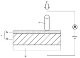
- Fig. 1B is a schematic diagram showing how to measure a withstand breakdown voltage of the insulating layer.
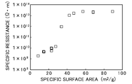
- Fig. 2A is a dispersion diagram showing a relationship between a specific surface area and the specific resistance of an anodized layer.
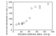
- Fig. 2B is a dispersion diagram showing a relationship between the specific surface area and the withstand breakdown voltage of the anodized layer.
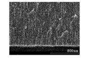
- Fig. 3A is an electron microscope photograph showing a cross section of the anodized layer according to sample No. 1.
- Fig. 3B is an electron microscope photograph showing a cross section of the anodized layer according to sample No. C1.
- An anodized layer according to the present invention has dramatically excellent insulation properties more than the conventional one. Although the present invention does not limit its morphology etc., it is considered that the morphology etc. of the anodized layer may change across a specific value (critical value) of the specific surface area as described above.
- the anodized layer according to the present invention is indirectly specified by using its specific surface area. Conversely, if anodized layers have the same specific surface area, they have the same morphologies etc.; this relationship is considered to be almost not influenced by the layer formation process as well as conditions and the layer thickness, etc. of the anodized layers.
- the specific resistance electrical resistivity
- the withstand voltage withstand breakdown voltage
- the layer thickness of the anodized layer is not limited, it should preferably be about 0.1 through 30 micrometers and, more preferably, about 1 through 20 micrometers in order to improve the slot space factor of the motor coil (conductor's net cross-sectional area/inter-iron core cross-sectional area) and the like while securing the insulation properties. If the layer thickness is too small, it is not preferable because sufficient insulation properties cannot be secured against high voltages, whereas if the layer thickness is too large, it is not preferable because cracks may easily occur when the layer is bent.
- a substrate according to the present invention is made of pure aluminum or aluminum alloy (hereinafter simply referred to as "aluminum"). Independently of the composition of aluminum, aluminum having a composition closer to that of pure aluminum is considered to be capable of more easily forming a uniform anodized layer.
- the conductor may be made of aluminum on its surface and of any other metal (copper etc.) on its inside.
- the substrate may have any given shapes and cross sections. It may be linear or columnar in shape or even circular or rectangular in cross section.
- Anodizing processing which is an insulating layer of the present invention, is formed by the anodizing processing by which the substrate is charged with electricity in an anodizing processing solvent (electrolytic solution).
- the anodizing processing solvent may be, for example, sulfuric acid aqueous solution, phosphoric acid aqueous solution, inorganic acid liquid such as chromium acid aqueous solution, or organic acid liquid such as oxalic acid aqueous solution.
- the sulfuric acid aqueous solution should have a concentration of about 5 through 40% by mass and, more preferably, about 10 through 35% by mass. If the concentration is too low, it is not preferable because the formation of the anodized layer is delayed, whereas if the concentration is too high, it is not preferable because the corrosion resistance of the anodized layer is deteriorated.
- the anodizing processing solvent in particular, sulfuric acid aqueous solution
- the voltage applied to the substrate which is an anode in the anodizing processing solvent
- the voltage applied to the substrate includes a DC voltage and a pulse voltage
- the value of the voltage should preferably be comparatively small.
- the specific voltage value cannot be specified because it depends on the type of the anodizing processing solvent, the electrical conductivity and the thickness of the substrate, etc., it should preferably be, for example, 2 through 15 V, 3 through 12 V, or 4 through 11 V.
- a cathode in the anodizing processing solvent may be made of either platinum or graphite.
- an anodizing processing lapse of time is appropriately adjusted in accordance with a desired layer thickness of the anodized layer, it should preferably, for example, be about 1 through 60 minutes and, more preferably, about 5 through 30 minutes.
- the anodized layer according to the present invention may be as anodized, it may subsequently undergo post-processing such as sealing, heat treatment, or coating appropriately.
- post-processing such as sealing, heat treatment, or coating appropriately.
- sealing processing fine pores formed in the anodized layer are sealed to improve the corrosion resistance of the insulation-covered aluminum conductor.
- the sealing processing is known and can be performed by, for example, exposing the anodized substrate to boiling water or high-pressure vapor.
- the specific resistance or the withstand voltage or the like of the anodized layer may fluctuate to some extent in the sealing processing, the anodized layer according to the present invention has remarkably excellent insulation properties, so that its insulation properties may be affected by the sealing processing relatively slightly.
- the insulating-layer-covered aluminum conductor of the present invention can be used arbitrarily. For example, it may be well suited for use as a motor coil or interconnection required to have high insulation properties.
- the insulating-layer-covered aluminum conductor of the present invention is well suited for use in a device required to have high insulation properties as well as a thinned insulating layer so that the slot space factor of the conductor is improved and heat generated in the conductor is radiated efficiently.
- ⁇ Manufacturing of sample>> (1) Substrate As a substrate forming an anodized layer, a disk-shaped test piece (25 mm (diameter) x 2 mm (thickness)) made of pure aluminum (JIS A1070) was prepared. The processing surface of the test piece forming the anodized layer had a surface roughness (Rz) of 1 micrometer.
- test piece was immersed in sulfuric acid aqueous solution (anodizing bath) to perform anodizing processing by performing electric charging between this test piece (processing surface) used as an anode and a platinum electrode used as a cathode.
- this test piece processing surface
- platinum electrode used as a cathode
- the surface of the test piece other than the processing surface was masked with insulating tape so that electric charging is conducted between the processing surface and the platinum electrode.
- concentration (% by mass) and the temperature of sulfuric acid in the anodizing bath and the voltage (layer formation voltage) applied between the electrodes were variously adjusted as shown in Table 1 to manufacture a plurality of samples. The samples all had an anodizing processing lapse of time of 10 minutes.
- the thickness (t) of the anodized layer 1a was obtained from a cross-sectional photograph of the sample 1 observed after the measurement of the specific resistance.
- the voltage value was measured 10 points for each sample. In each measurement, the terminal P was brought into contact with a different point on the anodized layer 1a. An arithmetic average value was obtained of the measured voltage values. The average value was divided by the thickness of the anodized layer 1a to obtain a withstand breakdown voltage value per unit thickness (referred to as "withstand breakdown voltage” simply). The thickness of the anodized layer 1a was obtained from the cross-sectional photograph of the sample after being measured as in the above-described case.
- the specific surface area (surface area per unit mass) of the anodized layer of each sample was obtained as follows. That is, first the sample after the measurement of the specific resistance and the withstand breakdown voltage was immersed in alkali solution to dissolve the substrate portion. The residue of the anodized layer obtained by filtering out the alkali solution was dried. The specific surface area of the residue was measured by BET nitrogen absorption described above.
- Table 1 shows the thus obtained specific resistance, withstand breakdown voltage, and specific surface area of each sample. Further, Figs. 2A and 2B respectively show the relationship between the specific surface area and the specific resistance and that between the specific surface area and the withstand breakdown voltage.
- FIGs. 3A and 3B respectively show the cross sections of the anodized layers of samples No. 1 and No. C1 observed with a field-emission-type scanning electron microscope (FE-SEM).
- FE-SEM field-emission-type scanning electron microscope
- an anodized layer having such a morphology as shown in Fig. 3A should preferably be formed on the surface of an aluminum-based substrate, which is a conductor.
Landscapes
- Chemical & Material Sciences (AREA)
- Engineering & Computer Science (AREA)
- Chemical Kinetics & Catalysis (AREA)
- Electrochemistry (AREA)
- Materials Engineering (AREA)
- Metallurgy (AREA)
- Organic Chemistry (AREA)
- Other Surface Treatments For Metallic Materials (AREA)
- Insulated Conductors (AREA)
- Laminated Bodies (AREA)
Abstract
An aluminum conductor having very high specific resistance and withstand breakdown voltage is provided. An aluminum conductor of the present invention includes a substrate made of pure aluminum or aluminum alloy and an insulating layer with which an outer surface of this substrate is covered, in which the insulating layer is composed of an anodized layer formed on the substrate and having a specific surface area of 25 m2/g or more. At the specific surface area of 25 m2/g or more, the specific resistance and the withstand breakdown voltage of the anodized layer rapidly rise exactly beyond comparison. The aluminum conductor covered with such an anodized layer exhibits high insulation properties. Moreover, the anodized layer has excellent heat resistance. Therefore, the aluminum conductor of the present invention exhibits excellent insulation properties even in a high temperature environment etc.
Description
The present invention relates to an insulating-layer-covered aluminum conductor which is covered with an anodized layer, an insulating layer formed of the anodized layer, and a method for forming the insulating layer.
A conductor (insulating-layer-covered conductor) has been used as an interconnection or a motor coil (wiring) or segment. The insulating-layer-covered conductor is represented by an enamel-coated conductor, besides which a lighter insulating-layer-covered aluminum conductor has been used recently. In this case, as the insulating layer, an anodized layer is utilized which is formed directly on the surface of the aluminum conductor. The anodized layer is made of aluminum oxide (alumite) and excellent in insulation properties and heat resistance. The excellence well qualifies the insulating-layer-covered aluminum conductor for use as an interconnection and a device which are subject to high voltages and high temperatures.
For such an insulating-layer-covered aluminum conductor, see the following Patent Literature 1, for example.
However, Patent Literature 1 describes nothing about to which extent the thus formed aluminum oxide film has an insulation resistance and a withstand voltage and discusses nothing about characteristics and insulation properties of this film.
In view of the above, the present invention has been developed, and it is an object of the present invention to provide an aluminum conductor (insulating-layer-covered aluminum conductor) which is insulation-covered with an anodized layer (aluminum oxide film) which is excellent in insulation properties more than the conventional one. It is another object of the present invention to provide this insulation layer and a method for forming it.
The present inventors have studied earnestly and conducted trial and error to solve those problems and, as a result, found newly that if the specific surface area of the anodized layer reaches a predetermined value (critical value), its insulation properties change rapidly. By developing the fruits, the inventors have completed the following invention.
<<Insulating-layer-covered aluminum conductor>>
(1) An insulating-layer-covered aluminum conductor of the present invention includes a substrate made of pure aluminum or aluminum alloy and an insulating layer with which the outer surface of the substrate is covered, which insulating layer is composed of an anodized layer formed on the substrate and having a specific surface area of 25 m2/g or more.
(1) An insulating-layer-covered aluminum conductor of the present invention includes a substrate made of pure aluminum or aluminum alloy and an insulating layer with which the outer surface of the substrate is covered, which insulating layer is composed of an anodized layer formed on the substrate and having a specific surface area of 25 m2/g or more.
(2) The anodized layer according to the present invention has very high insulation properties. Therefore, in contrast to the case of the conventional one, it is possible to improve the withstand breakdown voltage without changing the layer thickness of the insulating layer and, conversely, reduce the layer thickness of the insulating layer without changing the withstand breakdown voltage. For example, by reducing the thickness of the insulating layer formed of an anodized layer in the case of the latter, it is possible to improve the slot space factor and the radiation performance of the conductor itself as a whole.
(3) Although the mechanism is not totally clear of the excellent insulation properties of the anodized layer according to the present invention having a specific surface area of 25 m2/g or more, it is considered as follows presently. As long as the present inventors have studied earnestly, it is known that the anodized layer has different morphologies in a case where the specific surface area is smaller than 25 m2/g and in a case where it is larger than it. That is, in the case where the specific surface area is smaller than 25 m2/g, the anodized layer is composed of holes (straight hole) extending straight in the thickness direction as in the case of the conventional one. In the case where the specific surface area is 25 m2/g or more, the anodized layer is a porous body formed of an aggregate of non-straight porosities extending in the thickness direction. In such a manner, the morphology of the anodized layer changes across the particular specific surface area, so that its insulation properties such as the specific resistance and withstand breakdown voltage might possibly have changed rapidly beyond changes in creeping distance.
<<Insulating layer>>
The present invention can be grasped not only as an insulating-layer-covered aluminum conductor but also as an insulating layer formed of the above-described anodized layer with which the relevant aluminum conductor is covered.
The present invention can be grasped not only as an insulating-layer-covered aluminum conductor but also as an insulating layer formed of the above-described anodized layer with which the relevant aluminum conductor is covered.
<<Method for forming insulating layer>>
The present invention can also be grasped as a method for forming the insulating layer described above. That is, the present invention may be an insulating layer formation method that includes a layer formation step of forming the insulating layer by continuously applying a DC voltage to an anode composed of a substrate made of pure aluminum or aluminum alloy in an acid aqueous solution.
The present invention can also be grasped as a method for forming the insulating layer described above. That is, the present invention may be an insulating layer formation method that includes a layer formation step of forming the insulating layer by continuously applying a DC voltage to an anode composed of a substrate made of pure aluminum or aluminum alloy in an acid aqueous solution.
<<Others>>
(1) The specific surface area of the anodized layer referred to in the present description was specified on the basis of a calculated value by use of BET nitrogen absorption. That is, according to the method of fluxion (carrier gas method), the specific surface area was obtained by measurement in accordance with JIS Z8830:2001 by using helium as a non-adsorbed gas and nitrogen as an adsorbate. In this case, a sample was degasified at 100 degrees C for 30 minutes. Further, measured data was evaluated by the multipoint method. If the specific surface area is 30 m2/g or more, 35 m2/g or more, 40 m2/g or more, 45 m2/g or more, or 50 m2/g or more, it is preferable because an anodized layer having high insulation properties can be obtained more reliably.
(1) The specific surface area of the anodized layer referred to in the present description was specified on the basis of a calculated value by use of BET nitrogen absorption. That is, according to the method of fluxion (carrier gas method), the specific surface area was obtained by measurement in accordance with JIS Z8830:2001 by using helium as a non-adsorbed gas and nitrogen as an adsorbate. In this case, a sample was degasified at 100 degrees C for 30 minutes. Further, measured data was evaluated by the multipoint method. If the specific surface area is 30 m2/g or more, 35 m2/g or more, 40 m2/g or more, 45 m2/g or more, or 50 m2/g or more, it is preferable because an anodized layer having high insulation properties can be obtained more reliably.
(2) The "non-straight porosity" referred to in the present description about the morphology of the anodized layer is a porosity (cell) extending in the thickness direction and not having a smooth inner wall surface but having an irregular inner wall surface so that the anodized layer would be broken up in the thickness direction not between the cells but in the cell.
(3) Unless otherwise specified, in the present description, "x through y" includes the lower limit value x and the upper limit value y. A range "a through b" can be given newly by using various values or arbitrary values in a value range described in the present description as new arbitrary lower limit or upper limit values.
Description made in the present description may hold true not only with the insulating-layer-covered aluminum conductor of the present invention but also with an insulating layer and a method for forming it. Components related to the method can also be related to a physical object if they are understood on the basis of product-by-process claims. To the above-described components of the present invention, one or more components arbitrarily selected from the present description can be added. Which one of the embodiments is the best depends on a subject, required performance, and the like.
<<Anodized layer>>
An anodized layer according to the present invention has dramatically excellent insulation properties more than the conventional one. Although the present invention does not limit its morphology etc., it is considered that the morphology etc. of the anodized layer may change across a specific value (critical value) of the specific surface area as described above.
An anodized layer according to the present invention has dramatically excellent insulation properties more than the conventional one. Although the present invention does not limit its morphology etc., it is considered that the morphology etc. of the anodized layer may change across a specific value (critical value) of the specific surface area as described above.
It may not be easy to directly specify the morphology etc. of the anodized layer. Accordingly, in the present description, the anodized layer according to the present invention is indirectly specified by using its specific surface area. Conversely, if anodized layers have the same specific surface area, they have the same morphologies etc.; this relationship is considered to be almost not influenced by the layer formation process as well as conditions and the layer thickness, etc. of the anodized layers.
As something which indicates the insulation properties of the anodized layer that change rapidly in accordance with the specific surface area, the specific resistance (electrical resistivity) and the withstand voltage (withstand breakdown voltage), for example, are available. For example, across the critical value of the specific surface area, the withstand voltage of the anodized layer can change three- through six-fold and the specific resistance thereof, 100 (102) through 10000 (104)fold.
Although the layer thickness of the anodized layer is not limited, it should preferably be about 0.1 through 30 micrometers and, more preferably, about 1 through 20 micrometers in order to improve the slot space factor of the motor coil (conductor's net cross-sectional area/inter-iron core cross-sectional area) and the like while securing the insulation properties. If the layer thickness is too small, it is not preferable because sufficient insulation properties cannot be secured against high voltages, whereas if the layer thickness is too large, it is not preferable because cracks may easily occur when the layer is bent.
<<Substrate>>
A substrate according to the present invention is made of pure aluminum or aluminum alloy (hereinafter simply referred to as "aluminum"). Independently of the composition of aluminum, aluminum having a composition closer to that of pure aluminum is considered to be capable of more easily forming a uniform anodized layer.
A substrate according to the present invention is made of pure aluminum or aluminum alloy (hereinafter simply referred to as "aluminum"). Independently of the composition of aluminum, aluminum having a composition closer to that of pure aluminum is considered to be capable of more easily forming a uniform anodized layer.
Further, it is only necessary that a portion covered with the anodized layer should be made of aluminum, so that the entirety of the conductor need not be made of aluminum. For example, the conductor may be made of aluminum on its surface and of any other metal (copper etc.) on its inside.
Moreover, the substrate may have any given shapes and cross sections. It may be linear or columnar in shape or even circular or rectangular in cross section.
<<Method for formation>>
(1) Anodizing processing
The anodized layer, which is an insulating layer of the present invention, is formed by the anodizing processing by which the substrate is charged with electricity in an anodizing processing solvent (electrolytic solution). The anodizing processing solvent may be, for example, sulfuric acid aqueous solution, phosphoric acid aqueous solution, inorganic acid liquid such as chromium acid aqueous solution, or organic acid liquid such as oxalic acid aqueous solution. By the present invention, no matter which type of the anodizing processing solvent is used, it is preferable to use sulfuric acid aqueous solution from the viewpoint of the flexibility of the anodized layer and the economical efficiency of the processing. In this case, the sulfuric acid aqueous solution should have a concentration of about 5 through 40% by mass and, more preferably, about 10 through 35% by mass. If the concentration is too low, it is not preferable because the formation of the anodized layer is delayed, whereas if the concentration is too high, it is not preferable because the corrosion resistance of the anodized layer is deteriorated. Further, the anodizing processing solvent (in particular, sulfuric acid aqueous solution) should have a temperature of about 0 through 40 degrees C preferably and, more preferably, about 10 through 30 degrees C. If the temperature is too low, it is not preferable because the formation of the anodized layer is delayed, whereas if the temperature is too high, it is not preferable because the dissolution rate of the anodized layer is accelerated.
(1) Anodizing processing
The anodized layer, which is an insulating layer of the present invention, is formed by the anodizing processing by which the substrate is charged with electricity in an anodizing processing solvent (electrolytic solution). The anodizing processing solvent may be, for example, sulfuric acid aqueous solution, phosphoric acid aqueous solution, inorganic acid liquid such as chromium acid aqueous solution, or organic acid liquid such as oxalic acid aqueous solution. By the present invention, no matter which type of the anodizing processing solvent is used, it is preferable to use sulfuric acid aqueous solution from the viewpoint of the flexibility of the anodized layer and the economical efficiency of the processing. In this case, the sulfuric acid aqueous solution should have a concentration of about 5 through 40% by mass and, more preferably, about 10 through 35% by mass. If the concentration is too low, it is not preferable because the formation of the anodized layer is delayed, whereas if the concentration is too high, it is not preferable because the corrosion resistance of the anodized layer is deteriorated. Further, the anodizing processing solvent (in particular, sulfuric acid aqueous solution) should have a temperature of about 0 through 40 degrees C preferably and, more preferably, about 10 through 30 degrees C. If the temperature is too low, it is not preferable because the formation of the anodized layer is delayed, whereas if the temperature is too high, it is not preferable because the dissolution rate of the anodized layer is accelerated.
Although the voltage applied to the substrate, which is an anode in the anodizing processing solvent, includes a DC voltage and a pulse voltage, it is preferable to use a continuous DC voltage from the viewpoint of the rate of formation of the anodized layer and the economical efficiency of facilities. In this case, the value of the voltage should preferably be comparatively small. Although the specific voltage value cannot be specified because it depends on the type of the anodizing processing solvent, the electrical conductivity and the thickness of the substrate, etc., it should preferably be, for example, 2 through 15 V, 3 through 12 V, or 4 through 11 V. If the voltage is too low or too high, it is not preferable respectively because the formation of the anodized layer is delayed or the insulation properties and the flexibility of the anodized layer are deteriorated. A cathode in the anodizing processing solvent may be made of either platinum or graphite.
Although an anodizing processing lapse of time is appropriately adjusted in accordance with a desired layer thickness of the anodized layer, it should preferably, for example, be about 1 through 60 minutes and, more preferably, about 5 through 30 minutes.
(2) Post-processing
Although the anodized layer according to the present invention may be as anodized, it may subsequently undergo post-processing such as sealing, heat treatment, or coating appropriately. For example, by performing sealing processing, fine pores formed in the anodized layer are sealed to improve the corrosion resistance of the insulation-covered aluminum conductor. The sealing processing is known and can be performed by, for example, exposing the anodized substrate to boiling water or high-pressure vapor. Although the specific resistance or the withstand voltage or the like of the anodized layer may fluctuate to some extent in the sealing processing, the anodized layer according to the present invention has remarkably excellent insulation properties, so that its insulation properties may be affected by the sealing processing relatively slightly.
Although the anodized layer according to the present invention may be as anodized, it may subsequently undergo post-processing such as sealing, heat treatment, or coating appropriately. For example, by performing sealing processing, fine pores formed in the anodized layer are sealed to improve the corrosion resistance of the insulation-covered aluminum conductor. The sealing processing is known and can be performed by, for example, exposing the anodized substrate to boiling water or high-pressure vapor. Although the specific resistance or the withstand voltage or the like of the anodized layer may fluctuate to some extent in the sealing processing, the anodized layer according to the present invention has remarkably excellent insulation properties, so that its insulation properties may be affected by the sealing processing relatively slightly.
<<Use>>
The insulating-layer-covered aluminum conductor of the present invention can be used arbitrarily. For example, it may be well suited for use as a motor coil or interconnection required to have high insulation properties. In particular, the insulating-layer-covered aluminum conductor of the present invention is well suited for use in a device required to have high insulation properties as well as a thinned insulating layer so that the slot space factor of the conductor is improved and heat generated in the conductor is radiated efficiently.
The insulating-layer-covered aluminum conductor of the present invention can be used arbitrarily. For example, it may be well suited for use as a motor coil or interconnection required to have high insulation properties. In particular, the insulating-layer-covered aluminum conductor of the present invention is well suited for use in a device required to have high insulation properties as well as a thinned insulating layer so that the slot space factor of the conductor is improved and heat generated in the conductor is radiated efficiently.
The present invention will be described more specifically with reference to examples.
<<Manufacturing of sample>>
(1) Substrate
As a substrate forming an anodized layer, a disk-shaped test piece (25 mm (diameter) x 2 mm (thickness)) made of pure aluminum (JIS A1070) was prepared. The processing surface of the test piece forming the anodized layer had a surface roughness (Rz) of 1 micrometer.
(1) Substrate
As a substrate forming an anodized layer, a disk-shaped test piece (25 mm (diameter) x 2 mm (thickness)) made of pure aluminum (JIS A1070) was prepared. The processing surface of the test piece forming the anodized layer had a surface roughness (Rz) of 1 micrometer.
(2) Anodizing processing
The test piece was immersed in sulfuric acid aqueous solution (anodizing bath) to perform anodizing processing by performing electric charging between this test piece (processing surface) used as an anode and a platinum electrode used as a cathode. In this case, the surface of the test piece other than the processing surface was masked with insulating tape so that electric charging is conducted between the processing surface and the platinum electrode. The concentration (% by mass) and the temperature of sulfuric acid in the anodizing bath and the voltage (layer formation voltage) applied between the electrodes were variously adjusted as shown in Table 1 to manufacture a plurality of samples. The samples all had an anodizing processing lapse of time of 10 minutes. The samples taken out of the anodizing bath after the anodizing processing were all washed well with distilled water, blown with compressed air to remove their water contents sufficiently, and then dried in the atmosphere air for 24 hours. Each two out of the samples were manufactured for each of conditions shown in Table 1, to undergo the later-described measurement of specific resistance and withstand breakdown voltage.
The test piece was immersed in sulfuric acid aqueous solution (anodizing bath) to perform anodizing processing by performing electric charging between this test piece (processing surface) used as an anode and a platinum electrode used as a cathode. In this case, the surface of the test piece other than the processing surface was masked with insulating tape so that electric charging is conducted between the processing surface and the platinum electrode. The concentration (% by mass) and the temperature of sulfuric acid in the anodizing bath and the voltage (layer formation voltage) applied between the electrodes were variously adjusted as shown in Table 1 to manufacture a plurality of samples. The samples all had an anodizing processing lapse of time of 10 minutes. The samples taken out of the anodizing bath after the anodizing processing were all washed well with distilled water, blown with compressed air to remove their water contents sufficiently, and then dried in the atmosphere air for 24 hours. Each two out of the samples were manufactured for each of conditions shown in Table 1, to undergo the later-described measurement of specific resistance and withstand breakdown voltage.
<<Measurement and observation>>
(1) Specific resistance
The specific resistance (electrical resistivity) of each of the samples was obtained by using a method shown in Fig. 1A. That is, an electrode T1 having a diameter of 12.5 mm was attached via silver paste g to ananodized layer 1a generated on a substrate 1b of each sample 1. Further, an electrode T2 was attached to the opposite side surface of the substrate 1b. A DC voltage of 100 V was applied between those electrodes to measure a current flowing through a closed circuit. The measured current value (I), the applied voltage value (V), an electrode area (S1) of the electrode T1, and a thickness (t) of the anodized layer 1a were used to calculate a specific resistance (rho = (V/I) x S/t) based on Ohm's law. The thickness (t) of the anodized layer 1a was obtained from a cross-sectional photograph of the sample 1 observed after the measurement of the specific resistance.
(1) Specific resistance
The specific resistance (electrical resistivity) of each of the samples was obtained by using a method shown in Fig. 1A. That is, an electrode T1 having a diameter of 12.5 mm was attached via silver paste g to an
(2) Withstand breakdown voltage
As shown in Fig. 1B, the withstand breakdown voltage of each sample was measured in accordance with JIS H8687. That is, in the atmosphere, a terminal P whose contact end surface is shaped like a sphere having a diameter of 6 mm was brought into contact with theanodized layer 1a by applying a load F of 100 g. Between the terminal P and an electrode N attached on the opposite side of the substrate 1b, a DC voltage boosted at a rate of 25 V/s was applied. A voltage value was measured at a point in time when a leakage current flowing through the closed circuit exceeded 5 mA.
As shown in Fig. 1B, the withstand breakdown voltage of each sample was measured in accordance with JIS H8687. That is, in the atmosphere, a terminal P whose contact end surface is shaped like a sphere having a diameter of 6 mm was brought into contact with the
The voltage value was measured 10 points for each sample. In each measurement, the terminal P was brought into contact with a different point on the anodized layer 1a. An arithmetic average value was obtained of the measured voltage values. The average value was divided by the thickness of the anodized layer 1a to obtain a withstand breakdown voltage value per unit thickness (referred to as "withstand breakdown voltage" simply). The thickness of the anodized layer 1a was obtained from the cross-sectional photograph of the sample after being measured as in the above-described case.
(3) Specific surface area
The specific surface area (surface area per unit mass) of the anodized layer of each sample was obtained as follows. That is, first the sample after the measurement of the specific resistance and the withstand breakdown voltage was immersed in alkali solution to dissolve the substrate portion. The residue of the anodized layer obtained by filtering out the alkali solution was dried. The specific surface area of the residue was measured by BET nitrogen absorption described above.
The specific surface area (surface area per unit mass) of the anodized layer of each sample was obtained as follows. That is, first the sample after the measurement of the specific resistance and the withstand breakdown voltage was immersed in alkali solution to dissolve the substrate portion. The residue of the anodized layer obtained by filtering out the alkali solution was dried. The specific surface area of the residue was measured by BET nitrogen absorption described above.
Table 1 shows the thus obtained specific resistance, withstand breakdown voltage, and specific surface area of each sample. Further, Figs. 2A and 2B respectively show the relationship between the specific surface area and the specific resistance and that between the specific surface area and the withstand breakdown voltage.
(4) Morphology of anodized layer
Figs. 3A and 3B respectively show the cross sections of the anodized layers of samples No. 1 and No. C1 observed with a field-emission-type scanning electron microscope (FE-SEM).
Figs. 3A and 3B respectively show the cross sections of the anodized layers of samples No. 1 and No. C1 observed with a field-emission-type scanning electron microscope (FE-SEM).
<<Evaluation>>
(1) As may be seen from Table 1 and Figs. 2A and 2B, the specific resistance and the withstand breakdown voltage rapidly change critically near a specific surface area of 25 m2/g. That is, it was found that at the specific surface area of 25 m2/g or more, the specific resistance of the anodized layer would rapidly rise exactly beyond comparison, from the order of 109 (ohm-meter) to the order of 1010 through 1014 (ohm-meter).
(1) As may be seen from Table 1 and Figs. 2A and 2B, the specific resistance and the withstand breakdown voltage rapidly change critically near a specific surface area of 25 m2/g. That is, it was found that at the specific surface area of 25 m2/g or more, the specific resistance of the anodized layer would rapidly rise exactly beyond comparison, from the order of 109 (ohm-meter) to the order of 1010 through 1014 (ohm-meter).
It was found that this tendency holds true also with the withstand breakdown voltage in that at the specific surface area of 25 m2/g or more, the withstand breakdown voltage of the anodized layer rapidly rises up to about four-fold, from the order of 60 volt/micrometer to the order of up to 240 volt/micrometer.
(2) Such rapid changes in specific resistance and withstand breakdown voltage are considered to be caused by a change in morphology itself of the anodized layer as may be clear from the micrographs in Figs. 3A and 3B. That is, as shown in Fig. 3A, in a case where the anodized layer is a porous body formed of non-straight porosities having irregular surfaces, the specific surface area increases and the specific resistance and the withstand breakdown voltage increases rapidly. As shown in Fig. 3B, in a case where the anodized layer is a porous body formed of straight porosities, the specific surface area is relatively small and even if the specific surface area changes to some extent, both of the specific resistance and the withstand breakdown voltage stays low.
It is found that to obtain an insulating-layer-covered aluminum conductor by using such a layer having large values of the specific resistance and the withstand breakdown voltage, an anodized layer having such a morphology as shown in Fig. 3A should preferably be formed on the surface of an aluminum-based substrate, which is a conductor.

1 Sample (test piece)
1a Anodized layer
1b Substrate
1a Anodized layer
1b Substrate
Claims (4)
- An insulating-layer-covered aluminum conductor including a substrate made of pure aluminum or aluminum alloy and an insulating layer with which an outer surface of this substrate is covered, wherein the insulating layer is composed of an anodized layer formed on the substrate and having a specific surface area of 25 m2/g or more.
- The insulating-layer-covered aluminum conductor according to claim 1, wherein the anodized layer is a porous body formed of an aggregate of non-straight porosities extending in a thickness direction.
- An insulating layer formed of the anodized layer according to claim 1 or 2.
- A method for forming an insulating layer, the method comprising the layer formation step of continuously applying a DC voltage to a substrate made of pure aluminum or aluminum alloy by using this substrate as an anode in acid aqueous solution, thereby forming the insulating layer according to any one of claims 1 to 3.
Priority Applications (1)
| Application Number | Priority Date | Filing Date | Title |
|---|---|---|---|
| CN201280023203.1A CN103534390A (en) | 2011-05-18 | 2012-03-23 | Insulating-layer-covered aluminum conductor, and insulating layer and method for forming the insulating layer |
Applications Claiming Priority (2)
| Application Number | Priority Date | Filing Date | Title |
|---|---|---|---|
| JP2011-111570 | 2011-05-18 | ||
| JP2011111570A JP5522117B2 (en) | 2011-05-18 | 2011-05-18 | Insulating coated aluminum conductor, insulating coating and method for forming the same |
Publications (1)
| Publication Number | Publication Date |
|---|---|
| WO2012157164A1 true WO2012157164A1 (en) | 2012-11-22 |
Family
ID=45955062
Family Applications (1)
| Application Number | Title | Priority Date | Filing Date |
|---|---|---|---|
| PCT/JP2012/002056 Ceased WO2012157164A1 (en) | 2011-05-18 | 2012-03-23 | Insulating-layer-covered aluminum conductor, and insulating layer and method for forming the insulating layer |
Country Status (3)
| Country | Link |
|---|---|
| JP (1) | JP5522117B2 (en) |
| CN (1) | CN103534390A (en) |
| WO (1) | WO2012157164A1 (en) |
Cited By (2)
| Publication number | Priority date | Publication date | Assignee | Title |
|---|---|---|---|---|
| US20170047793A1 (en) * | 2015-08-11 | 2017-02-16 | Genesis Robotics Llp | Electric machine |
| US11549190B2 (en) * | 2018-07-31 | 2023-01-10 | Uacj Corporation | Aluminum member and method of manufacturing aluminum member |
Families Citing this family (4)
| Publication number | Priority date | Publication date | Assignee | Title |
|---|---|---|---|---|
| CN105886863A (en) * | 2016-06-07 | 2016-08-24 | 太仓市纯杰金属制品有限公司 | Heat-resisting aluminum alloy material for car |
| JP6585863B1 (en) * | 2019-01-23 | 2019-10-02 | 株式会社Uacj | Aluminum member and manufacturing method thereof |
| KR102935433B1 (en) * | 2021-11-05 | 2026-03-09 | 가부시키가이샤 아토1 | Aluminum metal material with excellent conductivity and method for manufacturing the same |
| JP2025038361A (en) * | 2023-09-07 | 2025-03-19 | 株式会社豊田中央研究所 | Coil member, its manufacturing method and armature |
Citations (3)
| Publication number | Priority date | Publication date | Assignee | Title |
|---|---|---|---|---|
| DE102004052563A1 (en) * | 2004-10-29 | 2006-05-04 | Interkat Katalysatoren Gmbh | Coating components with alumina comprises heating component coated with aluminum hydroxide prepared by adding excess aluminum or aluminum alloy to basic aqueous aluminate solution |
| US20080057293A1 (en) * | 2006-02-23 | 2008-03-06 | Fujifilm Corporation | Microstructure and method of manufacturing the same |
| JP2009099450A (en) | 2007-10-18 | 2009-05-07 | Yazaki Corp | Method for manufacturing aluminum oxide coated insulated aluminum wire |
Family Cites Families (5)
| Publication number | Priority date | Publication date | Assignee | Title |
|---|---|---|---|---|
| JP2002119856A (en) * | 2000-10-13 | 2002-04-23 | Hideo Kameyama | Alumite catalyst carrier having increased BET specific surface area and method for producing the same |
| JP2008127673A (en) * | 2006-11-24 | 2008-06-05 | Fujifilm Corp | Manufacturing method of fine structure and fine structure |
| JP2008144248A (en) * | 2006-12-13 | 2008-06-26 | Mitsui Mining & Smelting Co Ltd | Aluminum oxide anodized nanostructures |
| CN101210341B (en) * | 2006-12-30 | 2010-12-29 | 新疆众和股份有限公司 | Method for producing reaming electrolyte and high specific surface area aluminum electrolytic capacitor electrode foil |
| JP5544456B2 (en) * | 2007-09-21 | 2014-07-09 | 独立行政法人産業技術総合研究所 | Noble metal nanostructure and electrochemical reactor |
-
2011
- 2011-05-18 JP JP2011111570A patent/JP5522117B2/en active Active
-
2012
- 2012-03-23 WO PCT/JP2012/002056 patent/WO2012157164A1/en not_active Ceased
- 2012-03-23 CN CN201280023203.1A patent/CN103534390A/en active Pending
Patent Citations (3)
| Publication number | Priority date | Publication date | Assignee | Title |
|---|---|---|---|---|
| DE102004052563A1 (en) * | 2004-10-29 | 2006-05-04 | Interkat Katalysatoren Gmbh | Coating components with alumina comprises heating component coated with aluminum hydroxide prepared by adding excess aluminum or aluminum alloy to basic aqueous aluminate solution |
| US20080057293A1 (en) * | 2006-02-23 | 2008-03-06 | Fujifilm Corporation | Microstructure and method of manufacturing the same |
| JP2009099450A (en) | 2007-10-18 | 2009-05-07 | Yazaki Corp | Method for manufacturing aluminum oxide coated insulated aluminum wire |
Non-Patent Citations (2)
| Title |
|---|
| GANLEY J C ET AL: "Porous anodic alumina optimized as a catalyst support for microreactors", JOURNAL OF CATALYSIS, ACADEMIC PRESS, DULUTH, MN, US, vol. 227, no. 1, 1 October 2004 (2004-10-01), pages 26 - 32, XP004536788, ISSN: 0021-9517, DOI: 10.1016/J.JCAT.2004.06.016 * |
| ISMAGILOV I Z ET AL: "Optimization of anodic oxidation and Cu-Cr oxide catalyst preparation on structured aluminum plates processed by electro discharge machining", CATALYSIS TODAY, ELSEVIER, NL, vol. 105, no. 3-4, 15 August 2005 (2005-08-15), pages 516 - 528, XP004998999, ISSN: 0920-5861, DOI: 10.1016/J.CATTOD.2005.06.053 * |
Cited By (3)
| Publication number | Priority date | Publication date | Assignee | Title |
|---|---|---|---|---|
| US20170047793A1 (en) * | 2015-08-11 | 2017-02-16 | Genesis Robotics Llp | Electric machine |
| US9742225B2 (en) * | 2015-08-11 | 2017-08-22 | Genesis Robotics Llp | Electric machine |
| US11549190B2 (en) * | 2018-07-31 | 2023-01-10 | Uacj Corporation | Aluminum member and method of manufacturing aluminum member |
Also Published As
| Publication number | Publication date |
|---|---|
| CN103534390A (en) | 2014-01-22 |
| JP5522117B2 (en) | 2014-06-18 |
| JP2012241226A (en) | 2012-12-10 |
Similar Documents
| Publication | Publication Date | Title |
|---|---|---|
| Suzuki et al. | Corrosion-resistant porous alumina formed via anodizing aluminum in etidronic acid and its pore-sealing behavior in boiling water | |
| JP6681138B2 (en) | Stable solid electrolytic capacitors containing nanocomposites | |
| KR101049431B1 (en) | Capacitor and method of manufacturing the capacitor | |
| JP5522117B2 (en) | Insulating coated aluminum conductor, insulating coating and method for forming the same | |
| US20110020603A1 (en) | Capacitor and method for manufacturing the same | |
| JP2005002371A (en) | Aluminum foil, its production method, charge collector, secondary battery and electric double layer capacitor | |
| JP2025003611A (en) | Electrical Resistance Layer | |
| JP2007294875A (en) | Solid electrolytic capacitor | |
| JP2011162802A (en) | Method of manufacturing anodic oxidation film and electrolytic capacitor | |
| JP2015073015A (en) | Electrode foil, electrolytic capacitor and method for producing electrode foil | |
| JP2010212594A (en) | Solid electrolytic capacitor and its manufacturing method | |
| JP6036205B2 (en) | Insulation coated aluminum conductor and method of manufacturing the same | |
| WO2012035899A1 (en) | Solid electrolytic capacitor element, method for producing same, and tool for producing said solid electrolytic capacitor element | |
| WO2019176723A1 (en) | Solid electrolytic capacitor and method for manufacturing solid electrolytic capacitor | |
| JP5694888B2 (en) | Anisotropic conductive member and manufacturing method thereof | |
| KR20130076793A (en) | Method of manufacturing electrode structure, electrode structure, and capacitor | |
| JP5571753B2 (en) | Socket and jig for manufacturing capacitor element using the socket | |
| KR101573780B1 (en) | Electorde material containing multi-element metal oxide deposited electrode for supercapacitor and preparation method thereof | |
| Zahariev et al. | Effect of pore depth on thickening the barrier layer of porous anodic aluminum oxide | |
| CA3079667A1 (en) | Nanoelectronic activated circuit board metals | |
| JP5438485B2 (en) | Surface treatment member | |
| Baldhoff et al. | Characterization of Surface Films Formed on Aluminum during Mass-Transfer Limited Anodic Dissolution in Phosphoric Acid | |
| JP5091710B2 (en) | Solid electrolytic capacitor and manufacturing method thereof | |
| KR102794874B1 (en) | Materials of aluminum or its alloys and methods for manufacturing the same | |
| CN107170591A (en) | The manufacture method of capacitor |
Legal Events
| Date | Code | Title | Description |
|---|---|---|---|
| 121 | Ep: the epo has been informed by wipo that ep was designated in this application |
Ref document number: 12714400 Country of ref document: EP Kind code of ref document: A1 |
|
| NENP | Non-entry into the national phase |
Ref country code: DE |
|
| 122 | Ep: pct application non-entry in european phase |
Ref document number: 12714400 Country of ref document: EP Kind code of ref document: A1 |