WO2012148191A2 - Method for forming front electrode of solar cell - Google Patents
Method for forming front electrode of solar cell Download PDFInfo
- Publication number
- WO2012148191A2 WO2012148191A2 PCT/KR2012/003242 KR2012003242W WO2012148191A2 WO 2012148191 A2 WO2012148191 A2 WO 2012148191A2 KR 2012003242 W KR2012003242 W KR 2012003242W WO 2012148191 A2 WO2012148191 A2 WO 2012148191A2
- Authority
- WO
- WIPO (PCT)
- Prior art keywords
- electrode
- solution
- forming
- semiconductor layer
- front electrode
- Prior art date
Links
- 238000000034 method Methods 0.000 title claims abstract description 149
- 239000004065 semiconductor Substances 0.000 claims abstract description 217
- 229910052751 metal Inorganic materials 0.000 claims abstract description 78
- 239000002184 metal Substances 0.000 claims abstract description 78
- 238000007641 inkjet printing Methods 0.000 claims abstract description 60
- 238000007639 printing Methods 0.000 claims abstract description 28
- 238000005530 etching Methods 0.000 claims description 150
- 230000002209 hydrophobic effect Effects 0.000 claims description 119
- 239000000853 adhesive Substances 0.000 claims description 46
- 230000001070 adhesive effect Effects 0.000 claims description 46
- 239000000463 material Substances 0.000 claims description 44
- 238000004381 surface treatment Methods 0.000 claims description 31
- 238000003475 lamination Methods 0.000 claims description 16
- 238000009713 electroplating Methods 0.000 claims description 15
- 238000001312 dry etching Methods 0.000 claims description 3
- 238000007599 discharging Methods 0.000 claims 4
- 239000007767 bonding agent Substances 0.000 abstract 1
- 239000010408 film Substances 0.000 description 149
- 239000011521 glass Substances 0.000 description 14
- BQCADISMDOOEFD-UHFFFAOYSA-N Silver Chemical compound [Ag] BQCADISMDOOEFD-UHFFFAOYSA-N 0.000 description 12
- 229910052709 silver Inorganic materials 0.000 description 12
- 239000004332 silver Substances 0.000 description 12
- 229910052581 Si3N4 Inorganic materials 0.000 description 11
- XUIMIQQOPSSXEZ-UHFFFAOYSA-N Silicon Chemical compound [Si] XUIMIQQOPSSXEZ-UHFFFAOYSA-N 0.000 description 11
- 229910052710 silicon Inorganic materials 0.000 description 11
- 239000010703 silicon Substances 0.000 description 11
- HQVNEWCFYHHQES-UHFFFAOYSA-N silicon nitride Chemical compound N12[Si]34N5[Si]62N3[Si]51N64 HQVNEWCFYHHQES-UHFFFAOYSA-N 0.000 description 11
- 239000000758 substrate Substances 0.000 description 11
- 238000010586 diagram Methods 0.000 description 8
- 230000031700 light absorption Effects 0.000 description 7
- 239000000919 ceramic Substances 0.000 description 5
- 238000005304 joining Methods 0.000 description 5
- XLYOFNOQVPJJNP-UHFFFAOYSA-N water Substances O XLYOFNOQVPJJNP-UHFFFAOYSA-N 0.000 description 5
- 240000006829 Ficus sundaica Species 0.000 description 4
- 125000000217 alkyl group Chemical group 0.000 description 4
- 150000004767 nitrides Chemical class 0.000 description 4
- 238000007254 oxidation reaction Methods 0.000 description 4
- -1 alcohol fatty acid esters Chemical class 0.000 description 3
- 230000015572 biosynthetic process Effects 0.000 description 3
- 238000002508 contact lithography Methods 0.000 description 3
- 235000014113 dietary fatty acids Nutrition 0.000 description 3
- 229930195729 fatty acid Natural products 0.000 description 3
- 239000000194 fatty acid Substances 0.000 description 3
- 150000002894 organic compounds Chemical class 0.000 description 3
- 238000007650 screen-printing Methods 0.000 description 3
- 239000002904 solvent Substances 0.000 description 3
- CURLTUGMZLYLDI-UHFFFAOYSA-N Carbon dioxide Chemical compound O=C=O CURLTUGMZLYLDI-UHFFFAOYSA-N 0.000 description 2
- 238000005516 engineering process Methods 0.000 description 2
- 238000012827 research and development Methods 0.000 description 2
- 238000003915 air pollution Methods 0.000 description 1
- 229910002092 carbon dioxide Inorganic materials 0.000 description 1
- 239000001569 carbon dioxide Substances 0.000 description 1
- 238000006243 chemical reaction Methods 0.000 description 1
- 239000000470 constituent Substances 0.000 description 1
- 229910021419 crystalline silicon Inorganic materials 0.000 description 1
- 230000000694 effects Effects 0.000 description 1
- 230000007613 environmental effect Effects 0.000 description 1
- 239000002803 fossil fuel Substances 0.000 description 1
- 238000010438 heat treatment Methods 0.000 description 1
- 238000004519 manufacturing process Methods 0.000 description 1
- 239000003921 oil Substances 0.000 description 1
- 229920000620 organic polymer Polymers 0.000 description 1
- 239000002245 particle Substances 0.000 description 1
- 238000007747 plating Methods 0.000 description 1
- 230000003252 repetitive effect Effects 0.000 description 1
- 239000007787 solid Substances 0.000 description 1
- 239000010409 thin film Substances 0.000 description 1
- 238000010792 warming Methods 0.000 description 1
Images


Classifications
-
- H—ELECTRICITY
- H01—ELECTRIC ELEMENTS
- H01L—SEMICONDUCTOR DEVICES NOT COVERED BY CLASS H10
- H01L31/00—Semiconductor devices sensitive to infrared radiation, light, electromagnetic radiation of shorter wavelength or corpuscular radiation and specially adapted either for the conversion of the energy of such radiation into electrical energy or for the control of electrical energy by such radiation; Processes or apparatus specially adapted for the manufacture or treatment thereof or of parts thereof; Details thereof
- H01L31/04—Semiconductor devices sensitive to infrared radiation, light, electromagnetic radiation of shorter wavelength or corpuscular radiation and specially adapted either for the conversion of the energy of such radiation into electrical energy or for the control of electrical energy by such radiation; Processes or apparatus specially adapted for the manufacture or treatment thereof or of parts thereof; Details thereof adapted as photovoltaic [PV] conversion devices
-
- H—ELECTRICITY
- H01—ELECTRIC ELEMENTS
- H01L—SEMICONDUCTOR DEVICES NOT COVERED BY CLASS H10
- H01L31/00—Semiconductor devices sensitive to infrared radiation, light, electromagnetic radiation of shorter wavelength or corpuscular radiation and specially adapted either for the conversion of the energy of such radiation into electrical energy or for the control of electrical energy by such radiation; Processes or apparatus specially adapted for the manufacture or treatment thereof or of parts thereof; Details thereof
- H01L31/02—Details
- H01L31/0216—Coatings
- H01L31/02161—Coatings for devices characterised by at least one potential jump barrier or surface barrier
- H01L31/02167—Coatings for devices characterised by at least one potential jump barrier or surface barrier for solar cells
- H01L31/02168—Coatings for devices characterised by at least one potential jump barrier or surface barrier for solar cells the coatings being antireflective or having enhancing optical properties for the solar cells
-
- H—ELECTRICITY
- H01—ELECTRIC ELEMENTS
- H01L—SEMICONDUCTOR DEVICES NOT COVERED BY CLASS H10
- H01L31/00—Semiconductor devices sensitive to infrared radiation, light, electromagnetic radiation of shorter wavelength or corpuscular radiation and specially adapted either for the conversion of the energy of such radiation into electrical energy or for the control of electrical energy by such radiation; Processes or apparatus specially adapted for the manufacture or treatment thereof or of parts thereof; Details thereof
- H01L31/02—Details
- H01L31/0224—Electrodes
- H01L31/022408—Electrodes for devices characterised by at least one potential jump barrier or surface barrier
- H01L31/022425—Electrodes for devices characterised by at least one potential jump barrier or surface barrier for solar cells
-
- H—ELECTRICITY
- H01—ELECTRIC ELEMENTS
- H01L—SEMICONDUCTOR DEVICES NOT COVERED BY CLASS H10
- H01L31/00—Semiconductor devices sensitive to infrared radiation, light, electromagnetic radiation of shorter wavelength or corpuscular radiation and specially adapted either for the conversion of the energy of such radiation into electrical energy or for the control of electrical energy by such radiation; Processes or apparatus specially adapted for the manufacture or treatment thereof or of parts thereof; Details thereof
- H01L31/18—Processes or apparatus specially adapted for the manufacture or treatment of these devices or of parts thereof
-
- Y—GENERAL TAGGING OF NEW TECHNOLOGICAL DEVELOPMENTS; GENERAL TAGGING OF CROSS-SECTIONAL TECHNOLOGIES SPANNING OVER SEVERAL SECTIONS OF THE IPC; TECHNICAL SUBJECTS COVERED BY FORMER USPC CROSS-REFERENCE ART COLLECTIONS [XRACs] AND DIGESTS
- Y02—TECHNOLOGIES OR APPLICATIONS FOR MITIGATION OR ADAPTATION AGAINST CLIMATE CHANGE
- Y02E—REDUCTION OF GREENHOUSE GAS [GHG] EMISSIONS, RELATED TO ENERGY GENERATION, TRANSMISSION OR DISTRIBUTION
- Y02E10/00—Energy generation through renewable energy sources
- Y02E10/50—Photovoltaic [PV] energy
Definitions
- the present invention relates to a method for forming a front electrode of a solar cell, and more particularly, when printing an etching solution in the step of etching the anti-reflection film, or when printing an electrode solution or a conductive solution for forming the front electrode, EHD, Electrohydrodynamic (Ink Jetting Type) solution is printed, by reducing the width of the front electrode printed on the semiconductor layer of the solar cell to provide a high aspect ratio front electrode, the light incident to the solar cell It relates to a method of forming a front electrode of a solar cell to increase the amount of.
- the solar cell is a device that converts light energy into electrical energy by using the photovoltaic effect. It has the advantages of pollution-free, indefinite resource, and semi-permanent life. It is expected to be an energy source that can be solved.
- Solar cells may be classified into silicon solar cells, thin film solar cells, dye-sensitized solar cells, organic polymer solar cells, and the like according to their constituent materials.
- crystalline silicon solar cells account for most of the total production of solar cells in the world, and the photoelectric conversion efficiency is higher than other cells, and the technology is continuously being developed, which is the most popular solar cell.
- a solar cell includes an n-type semiconductor layer on a front surface of a silicon substrate and a p-type semiconductor layer on a rear surface thereof to form a pn junction interface.
- the semiconductor layer S is formed to contain.
- An antireflection film AR is coated on the front surface of the semiconductor layer S to minimize reflection of light incident on the solar cell, and the front electrode FE is wired to contact the semiconductor layer S.
- the rear electrode BE is wired on the rear surface of the semiconductor layer S.
- the solar cell generates charges (holes, electrons) by the incident light, and the generated charges are separately collected through the front electrode FE and the rear electrode BE to generate electrical energy.
- the generated electrical energy increases.
- the distance between the front electrodes FE spaced apart from each other should be widened.
- a method of reducing the electrode width w of the front electrode FE has been sought to widen the interval between the front electrodes FE.
- the front electrode is used to reduce the electrode width (w) of the front electrode as the electrode solution having a viscosity of 30000 cp to 150000 cp is printed by a contact printing method such as screen printing. There is a limit.
- the amount of charge transferred through the front electrode is proportional to the cross-sectional area of the front electrode (the product of the electrode width (w) and the height of the electrode (h)), reducing the electrode width (w) at the same electrode height (h) There is a problem that the electrical resistance increases.
- the contact printing method such as screen printing has a problem in that the semiconductor layer is damaged during the process, and thus, non-contact printing such as ink jetting to eject ink through the nozzle Law is required.
- the maximum viscosity of the electrode solution discharged in piezoelectric ink jetting or thermoelectric ink jetting is about 30 cP, there is a limit in printing the electrode solution having the aforementioned viscosity (30000 cps to 150000 cps).
- the size of the solid particles contained in the electrode solution is nanoscale, there are problems such as clogging of the nozzle.
- the diameter of the nozzle may be expanded to prevent nozzle clogging, but when the diameter of the nozzle is expanded in the conventional ink jetting, it is difficult to implement a desired minute electrode width w.
- an object of the present invention is to solve such a conventional problem, by reducing the electrode width of the front electrode, and by increasing the distance between the adjacent front electrode, the solar cell which can increase the amount of light incident on the solar cell
- the present invention provides a method for forming a front electrode.
- the method of forming the front electrode of the solar cell can maintain or increase the amount of charge that is transferred through the front electrode, and can reduce the electrical resistance generated in the front electrode In providing.
- the present invention provides a method for forming a front electrode of a solar cell that can prevent damage to a semiconductor layer while using an electrode solution having a viscosity of 30000cp to 150000cp as it is.
- the present invention provides a method for forming a front electrode of a solar cell that can implement a desired minute electrode width.
- the present invention provides a method for forming a front electrode of a solar cell capable of forming a front electrode having a high aspect ratio.
- a method for forming a front electrode on the front surface of a semiconductor layer of a solar cell the electrode forming step of printing an electrode solution on the front surface of the semiconductor layer;
- the electrode solution is a material mixed with the adhesive for bonding the semiconductor layer and the metal, the metal for forming the front electrode, the electrode forming step is at least one electrohydrodynamic (EHD, Electrohydrodynamic ) Forming a front electrode of a solar cell, characterized in that the charge is applied to the electrode solution by a power source applied using an ink jetting type, and the electrode solution having a charge from the nozzle is discharged by an electrostatic force. Is achieved by the method.
- EHD Electrohydrodynamic
- a surface treatment step of applying an anti-reflection film to the entire surface of the semiconductor layer to prevent reflection loss of incident light It is preferable to further include.
- the object is, according to the present invention, a method for forming a front electrode on a solar cell coated with an antireflection film on the entire surface of the semiconductor layer, the etching step of printing an etching solution on the antireflection film; An electrode forming step of printing an electrode solution on a portion where the anti-reflection film is etched through the etching step; An electrode curing step of curing the electrode solution such that the electrode solution printed on the portion where the anti-reflection film is etched through the electrode forming step becomes the front electrode; Including, The electrode solution is a material mixed with an adhesive for bonding the semiconductor layer and the metal, and the metal for forming the front electrode, wherein the etching step and the electrode forming step is at least one electrohydrodynamic (EHD, Electrohydrodynamic) The etching solution and the electrode solution by applying a power applied by using the ink jetting type (Ink Jetting Type), each of the etching solution and the electrode having a charge in each nozzle with an electrostatic force It
- a method for forming a front electrode on a solar cell coated with an antireflection film on the entire surface of the semiconductor layer comprising: etching the antireflection film by dry etching using a laser or plasma; An electrode forming step of printing an electrode solution on a portion where the anti-reflection film is etched through the etching step; An electrode curing step of curing the electrode solution such that the electrode solution printed on the portion where the anti-reflection film is etched through the electrode forming step becomes the front electrode;
- the electrode solution is a material mixed with the adhesive for bonding the semiconductor layer and the metal, the metal for forming the front electrode, the electrode forming step is at least one electrohydrodynamic (EHD, Electrohydrodynamic ) Forming a front electrode of a solar cell, characterized in that the charge is applied to the electrode solution by a power source applied using an ink jetting type, and the electrode solution having a charge from the nozzle is discharged by an electrostatic force.
- EHD Electrohydrodynamic
- a hydrophobic layer is formed by applying a hydrophobic material on the antireflection film to form a hydrophobic layer step; An etching step of printing an etching solution on the hydrophobic layer; Removing the hydrophobic layer and applying heat to the hydrophobic layer so that the etching solution printed through the etching step etches the anti-reflection film; An electrode forming step of printing an electrode solution on a portion where the anti-reflection film is etched through the hydrophobic layer removing step; An electrode curing step of curing the electrode solution such that the electrode solution printed on the portion where the anti-reflection film is etched through the electrode forming step becomes the front electrode; Including, The electrode solution is a material mixed with an adhesive for bonding the semiconductor layer and the metal, and the metal for forming the front electrode, wherein the etching step and the electrode forming
- an electrode for printing a conductive solution mixed with an etching solution and an electrode solution on the antireflection film Forming step An electrode curing step of curing the conductive solution such that the conductive solution printed on the antireflection film becomes the front electrode through the electrode forming step;
- the electrode solution is a material mixed with the adhesive for bonding the semiconductor layer and the metal, the metal for forming the front electrode, the electrode forming step is at least one electrohydrodynamic (EHD, Electrohydrodynamic ) Forming a front electrode of a solar cell, characterized in that the charge is applied to the conductive solution by a power source applied using an ink jetting type, and the conductive solution having a charge from the nozzle is discharged by electrostatic force. Is achieved by the method.
- EHD Electrohydrodynamic
- a hydrophobic layer is formed by applying a hydrophobic material on the antireflection film to form a hydrophobic layer step;
- the electrode solution is a material mixed with the adhesive for bonding the semiconductor layer and the metal, the metal for forming the front electrode, the electrode forming step is at least one electrohydrodynamic (EHD, Electrohydrodynamic ) Forming a front electrode of a solar cell, characterized in that the charge is applied
- the object is, according to the present invention, a method for forming a front electrode on a solar cell coated with an antireflection film on the entire surface of the semiconductor layer, the etching step of printing an etching solution on the antireflection film;
- Including, but the etching step is to charge the etching solution by a power applied by using one or more times (EHD, Electrohydrodynamic) ink jetting type (EHD Jet Inking Type), the charge in the nozzle by the electrostatic force It is achieved by a method for forming a front electrode of a solar cell, characterized in that the etching solution having a discharge.
- a hydrophobic layer is formed by applying a hydrophobic material on the antireflection film to form a hydrophobic layer step; An etching step of printing an etching solution on the hydrophobic layer; Removing the hydrophobic layer and applying heat to the hydrophobic layer so that the etching solution printed through the etching step etches the anti-reflection film; An auxiliary electrode forming step of forming the front electrode on the portion where the anti-reflection film is etched through the hydrophobic layer removing step by at least one electroplating method; Including, wherein the electrode solution is a material mixed with the adhesive for bonding the semiconductor layer and the metal, and the metal for forming the front electrode, the etching step is at least one electrohydrodynamic (EHD, Electrohydrodynamic) A method of forming a front electrode of a solar cell, characterized in that charge
- auxiliary electrode forming step of performing at least one electroplating with a metal for forming the front electrode on the portion where the anti-reflection film is etched It is preferable to further include.
- a method for forming a front electrode of a solar cell which can increase the amount of light incident on the solar cell by reducing the electrode width of the front electrode and widening the distance between adjacent front electrodes.
- the method of forming the front electrode of the solar cell can maintain or increase the amount of charge that is transferred through the front electrode, and can reduce the electrical resistance generated in the front electrode This is provided.
- an electrode solution having a viscosity of 100 cps to 150000 cps may be used, and a method of forming a front electrode of a solar cell capable of preventing breakage of a semiconductor layer is provided.
- a method of forming a front electrode of a solar cell capable of realizing a desired fine electrode width is provided.
- a method for forming a front electrode of a solar cell capable of reducing the contact area of the printed solution and improving the reduction of the electrode width according to the printed solution.
- a method of forming a front electrode of a solar cell which improves precision of front electrode formation and secures a high aspect ratio of the front electrode, is provided.
- EHD electrohydrodynamic ink jetting type
- FIG. 1 is a view schematically showing the structure of a typical solar cell
- FIG. 2 is a flowchart illustrating a first method of forming a front electrode on a solar cell according to an embodiment of the present invention
- 3 and 4 are flowcharts for explaining a second method and a third method of forming a front electrode in a solar cell according to an embodiment of the present invention
- FIG. 5 is a process flow diagram for a second method of forming a front electrode on a solar cell according to one embodiment of the present invention.
- FIG. 6 is a process flow diagram for a third method of forming a front electrode on a solar cell according to one embodiment of the present invention.
- FIG. 7 is a flowchart illustrating a fourth method and a fifth method of forming a front electrode on a solar cell according to an embodiment of the present invention
- FIG. 8 is a flowchart illustrating a sixth method and a seventh method of forming a front electrode on a solar cell according to an embodiment of the present invention
- FIG. 9 is a process flow diagram for a sixth method of forming a front electrode on a solar cell according to one embodiment of the present invention.
- FIG. 10 is a process flow diagram for a seventh method of forming a front electrode on a solar cell according to one embodiment of the present invention.
- the semiconductor layer S is formed to include a pn junction interface by forming an n-type semiconductor layer on a front surface of a silicon substrate and a p-type semiconductor layer on a rear surface of the silicon substrate.
- the front surface of the semiconductor layer S is coated with an antireflection film AR, and the front electrode FE is wired to contact the semiconductor layer S.
- the rear electrode BE is wired on the rear surface of the semiconductor layer S.
- the solar cell generates charges (holes, electrons) by the incident light, and the generated charges are separately collected through the front electrode FE and the rear electrode BE to generate electrical energy.
- the electrohydrodynamic (EHD, Electrohydrodynamic) ink jetting Charge is applied to the solution by a power source applied using an ink jetting type, and a solution having a charge from the nozzle N is discharged by electrostatic force to be printed on the semiconductor layer S.
- EHD Electrohydrodynamic
- the electrode solution E2 when the antireflection film AR is applied to the semiconductor layer S, the electrode solution E2 must be printed after undergoing an etching step.
- the method of forming the front electrode of the solar cell according to the exemplary embodiment of the present invention is a method for forming the front electrode FE in the semiconductor layer S of the solar cell, and can be classified into seven methods as follows.
- the first method is a method of printing the electrode solution (E2) directly on the semiconductor layer (S), and curing the printed electrode solution (E2) to form a front electrode (FE) in the solar cell.
- the electrode solution E2 has a viscosity of about 100 cP to 150000 cP, and may be formed in the form of a paste.
- the electrode solution E2 is a material in which a metal for forming the front electrode FE and an adhesive for joining the ceramic (semiconductor layer S) and the metal are mixed.
- glass frit is used as an adhesive
- silver (Ag) is generally used as a metal for forming the front electrode FE, but the type of adhesive or metal is limited. no.
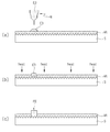
- FIG. 2 is a flowchart illustrating a first method of forming a front electrode on a solar cell according to an embodiment of the present invention.
- the first method of forming the front electrode FE in the solar cell includes a semiconductor forming step S1, an electrode forming step S7, and an electrode curing step S8.
- the semiconductor layer S is formed to generate charges (holes, electrons) by incident light.
- the semiconductor layer S is formed by forming an n-type semiconductor layer on the front surface of the silicon substrate and a p-type semiconductor layer on the rear surface thereof to include a pn junction interface. Then, the n-type semiconductor layer on the front surface acts as an emitter.
- the electrode forming step S7 is for forming the front electrode FE through which charges (holes, electrons) generated in the semiconductor layer S can move.
- the electrode solution E2 is printed on the entire surface of the semiconductor layer S formed through the semiconductor forming step S1. Since the electrode solution E2 forms the front electrode FE through the electrode curing step S8 described later, the electrode solution E2 should be printed in consideration of the pattern of the front electrode FE to be formed. In the electrode forming step S7, it is advantageous to be repeated one or more times in consideration of the electrode height h of the front electrode FE to be formed.
- the electrode solution E2 is charged by a power applied by using an electrohydrodynamic ink jetting type (EHD).
- the electrode solution E2 having the electric charge is discharged from the nozzle N by the electrostatic force.
- the electrode solution E2 may be discharged without clogging the nozzle N by using an electrohydrodynamic ink jetting type (EHD) even though the electrode solution E2 has a viscosity of about 1000 cp to 150000 cp.
- the electrode solution E2 having a viscosity of 20000 cp or more is discharged.
- the electrohydrodynamic ink jetting type may allow the size of the droplets discharged from the nozzle N to be smaller than the diameter of the nozzle N.
- FIG. Accordingly, when the above-described electrode solution E2 is discharged from the nozzle N, the droplet size of the discharged electrode solution E2 can be adjusted according to the applied power, and thus the electrode width of the front electrode FE to be formed. In consideration of (w), a desired electrode width w can be set.
- the electrode solution E2 printed on the semiconductor layer S is cured through the electrode forming step S7.
- the curing temperature of silver (Ag) in the metal for forming the front electrode (FE) in the electrode solution (E2) is about 200 degrees (°C)
- the curing temperature of the glass frit in the adhesive is about 700 degrees (°C). ) to be. Accordingly, in the electrode curing step S8, it is advantageous to heat the entire surface of the semiconductor layer S at 700 ° C. or more.
- the front electrode FE is formed on the entire surface of the semiconductor layer S.
- FIG. The electrode curing step S8 may be repeated one or more times in engagement with the electrode forming step S7 which is repeated in consideration of the height h of the front electrode FE to be formed.
- the first method of forming the front electrode FE on the solar cell may further include at least one of the surface treatment step S3 and the texturing step S2.
- an antireflection film AR is coated on the entire surface of the semiconductor layer S to prevent reflection of light incident to the solar cell and to prevent loss of incident light.
- the antireflection film AR may be coated on the entire surface of the semiconductor layer S to cover the front electrode FE stacked on the semiconductor layer S. In addition, it may be applied only between the front electrode FE formed in the semiconductor layer (S).
- the anti-reflection film AR formed in the surface treatment step S3 may use silicon nitride.
- the texturing step S2 irregularities are formed on the entire surface of the semiconductor layer S formed in the semiconductor forming step S1. If irregularities are formed on the entire surface of the semiconductor layer S through the texturing step S2, light absorption may be improved with respect to incident light, and the generation of charges (holes and electrons) may be promoted in the semiconductor layer S. have.
- the front surface of the semiconductor layer S may be hydrophilic to enhance adhesion between the semiconductor layer S and the anti-reflection film AR in the surface treatment step S3.
- the antireflection film AR is etched with the etching solution E1 while the antireflection film AR is formed on the semiconductor layer S, and then the electrode solution E2 is etched on the etched portion of the antireflection film AR. ), And the front electrode FE is formed on the solar cell by curing the printed electrode solution E2.
- the etching solution E1 may be a material capable of removing the contacted antireflection film AR.
- the electrode solution E2 has a viscosity of about 100 cP to 150000 cP, and may be formed in the form of a paste.
- the electrode solution E2 is a material in which a metal for forming the front electrode FE and an adhesive for joining the ceramic (semiconductor layer S) and the metal are mixed.
- glass frit is used as an adhesive
- silver (Ag) is generally used as a metal for forming the front electrode FE, but the type of adhesive or metal is limited. no.
- FIG. 3 and 4 are flowcharts illustrating a second method and a third method of forming a front electrode on a solar cell according to an embodiment of the present invention
- FIG. 5 is an embodiment according to an embodiment of the present invention. This is a process flow diagram for the second method of forming a front electrode in a cell.
- the semiconductor forming step S1 the surface treatment step S3, the etching step S5, and the electrode forming step (S7) and the electrode curing step (S8).
- the semiconductor layer S is formed to generate charges (holes, electrons) by incident light.
- the semiconductor layer S is formed by forming an n-type semiconductor layer on the front surface of the silicon substrate and a p-type semiconductor layer on the rear surface thereof to include a pn junction interface. Then, the n-type semiconductor layer on the front surface acts as an emitter.
- an antireflection film AR is coated on the entire surface of the semiconductor layer S to prevent reflection of light incident to the solar cell and to prevent loss of incident light.
- the antireflection film AR is applied to the entire surface of the semiconductor layer S.
- the anti-reflection film AR formed in the surface treatment step S3 may use silicon nitride.
- the etching solution E1 is printed on the antireflection film AR as shown in FIG. 5A. Then, as shown in (b) of FIG. 5, the antireflection film AR of the portion in contact with the etching solution E1 is etched to form a pattern for forming the front electrode FE.
- the etching step S5 may be repeated one or more times in consideration of the thickness of the antireflection film AR or the electrode width w of the front electrode FE to be formed.
- etching solution (E1) In order to print the etching solution (E1) in the etching step (S5), charge is applied to the etching solution (E1) by a power applied by using an electrohydrodynamic (EHD, Electro Hydrodynamic) ink jetting type (EHD), The etching solution E1 having an electric charge is discharged from the nozzle N by the electrostatic force.
- the etching solution E1 has a viscosity of about 100 cp or more or about 300 cp or more to be discharged by an electrohydrodynamic ink jetting type (EHD).
- the electrohydrodynamic ink jetting type (EHD) may allow the size of the droplets discharged from the nozzle N to be smaller than the diameter of the nozzle N.
- the droplet size of the etching solution E1 discharged according to the applied power can be adjusted, so that the electrode width w of the front electrode FE to be formed
- the anti-reflection film AR may be etched at a desired portion.
- the electrode forming step S7 is for forming the front electrode FE through which charges (holes, electrons) generated in the semiconductor layer S can move.
- the electrode forming step S7 prints the electrode solution E2 on the portion where the antireflection film AR is etched through the etching step S5 as shown in FIG. 5C. Since the electrode solution E2 forms the front electrode FE through the electrode curing step S8 described later, the electrode solution E2 should be printed in consideration of the pattern of the front electrode FE to be formed. In the electrode forming step S7, it is advantageous to be repeated one or more times in consideration of the electrode height h of the front electrode FE to be formed.
- the electrode solution E2 is charged by a power applied by using an electrohydrodynamic ink jetting type (EHD).
- the electrode solution E2 having the electric charge is discharged from the nozzle N by the electrostatic force.
- the electrode solution E2 may be discharged without clogging the nozzle N by using an electrohydrodynamic ink jetting type (EHD) even though the electrode solution E2 has a viscosity of about 1000 cp to 150000 cp.
- the electrode solution E2 having a viscosity of 20000 cp or more is discharged.
- the electrohydrodynamic ink jetting type may allow the size of the droplets discharged from the nozzle N to be smaller than the diameter of the nozzle N.
- FIG. Accordingly, when the above-described electrode solution E2 is discharged from the nozzle N, the droplet size of the discharged electrode solution E2 can be adjusted according to the applied power, and thus the electrode width of the front electrode FE to be formed. In consideration of (w), a desired electrode width w can be set.
- the electrode forming step S7 when the above-described etching step S5 etches the antireflection film AR by dry etching using a laser or plasma, the electrode forming step S7 must be performed using an electrohydrodynamic ink jetting method (EHD). Ink Jetting Type) is used.
- EHD electrohydrodynamic ink jetting Type
- the electrode curing step S8 cures the electrode solution E2 printed on the portion where the anti-reflection film AR is etched through the electrode forming step S7.
- the curing temperature of silver (Ag) in the metal for forming the front electrode (FE) in the electrode solution (E2) is about 200 degrees (°C)
- the curing temperature of the glass frit in the adhesive is about 700 degrees (°C). ) to be. Accordingly, in the electrode curing step S8, it is advantageous to heat the entire surface of the semiconductor layer S at 700 ° C. or higher as shown in FIG. 5D.
- the glass frit in the adhesive causes an oxidation reaction with silicon nitride (nitride) used as the antireflection film (AR) during the curing process, thereby causing the antireflection film (AR) to be etched. You can get it.
- the front electrode FE is formed on the entire surface of the semiconductor layer S as shown in FIG.
- the electrode curing step S8 may be repeated one or more times in engagement with the electrode forming step S7 which is repeated in consideration of the height h of the front electrode FE to be formed.
- the second method of forming the front electrode FE in the solar cell may further include at least one of the texturing step S2 and the auxiliary electrode forming step S7-1.
- the texturing step S2 irregularities are formed on the entire surface of the semiconductor layer S formed in the semiconductor forming step S1. If irregularities are formed on the entire surface of the semiconductor layer S through the texturing step S2, light absorption may be improved with respect to incident light, and the generation of charges (holes and electrons) may be promoted in the semiconductor layer S. have.
- the front surface of the semiconductor layer S may be hydrophilic to enhance adhesion between the semiconductor layer S and the anti-reflection film AR in the surface treatment step S3.
- the auxiliary electrode forming step S7-1 is to form the front electrode FE through which charges (holes, electrons) generated in the semiconductor layer S can move.
- the metal for forming the front electrode FE is formed by electroplating on a portion where the anti-reflection film AR is etched through the etching step S5 as shown in FIG. 3. May be plated.
- the auxiliary electrode forming step (S7-1) is a method of electroplating the electrode solution (E2) cured in the portion where the anti-reflection film (AR) is etched through the electrode curing step (S8) as shown in FIG.
- the metal for forming the front electrode FE may be plated.
- the electrical conductivity may be improved by increasing the purity of the front electrode FE.
- the third method is to apply the hydrophobic layer HP on the antireflection film AR in a state where the antireflection film AR is formed on the semiconductor layer S, and then print the etching solution E1 on the hydrophobic layer HP. Then, the etching solution E1 etches the antireflection film AR while the hydrophobic layer HP is removed, the electrode solution E2 is printed on the etched portion of the antireflection film AR, and the printed electrode solution E2 is printed. ) To form a front electrode (FE) in the solar cell.
- FE front electrode
- the material forming the hydrophobic layer (HP) may be an organic compound consisting of monohydric or dihydric alcohol fatty acid esters, it may be used a wax containing an alkyl chain (alkyl chain).
- the etching solution E1 is sufficient to be a material capable of removing the antireflection film AR in contact.
- the electrode solution E2 has a viscosity of about 100 cP to 150000 cP, and may be formed in the form of a paste.
- the electrode solution E2 is a material in which a metal for forming the front electrode FE and an adhesive for joining the ceramic (semiconductor layer S) and the metal are mixed.
- glass frit is used as an adhesive
- silver (Ag) is generally used as a metal for forming the front electrode FE, but the type of adhesive or metal is limited. no.
- FIG. 3 and 4 are flowcharts illustrating a second method and a third method of forming a front electrode in a solar cell according to an embodiment of the present invention
- FIG. 6 is an embodiment according to an embodiment of the present invention.
- the semiconductor forming step S1 the surface treatment step S3, the hydrophobic lamination step S4, , An etching step S5, a hydrophobic layer removing step S6, an electrode forming step S7, and an electrode curing step S8.
- the semiconductor layer S is formed to generate charges (holes, electrons) by incident light.
- the n-type semiconductor layer is formed on the front surface of the silicon substrate and the p-type semiconductor layer is formed on the rear surface of the semiconductor substrate to form the pn junction interface. Then, the n-type semiconductor layer on the front surface acts as an emitter.
- an antireflection film AR is coated on the entire surface of the semiconductor layer S to prevent reflection of light incident to the solar cell and to prevent loss of incident light.
- the antireflection film AR may be applied to the entire surface of the semiconductor layer S.
- the anti-reflection film AR formed in the surface treatment step S3 may use silicon nitride.
- a hydrophobic material is coated on the antireflection film AR to form a hydrophobic layer HP.
- the hydrophobic layer HP formed on the anti-reflection film AR through the hydrophobic lamination step S4 is evaporated at a low temperature (lower than the temperature for curing the electrode solution), and is soluble in water-soluble (water soluble) or oily solvents. It is advantageous to have the property of not dissolving.
- heat may be applied to the hydrophobic material, and the heated hydrophobic material may be sprayed onto the antireflection film AR.
- the etching solution E1 is printed on the hydrophobic layer HP as shown in FIG. 6B.
- the contact area between the hydrophilic etching solution E1 and the hydrophobic layer HP can be reduced.
- the etching width of the antireflection film AR may be reduced, and the electrode of the front electrode FE formed on the etched portion of the antireflection film AR as the etching width of the antireflection film AR is reduced.
- the width w may also be reduced, thereby increasing the amount of light incident on the solar cell.
- etching solution (E1) In order to print the etching solution (E1) in the etching step (S5), charge is applied to the etching solution (E1) by a power applied by using an electrohydrodynamic (EHD, Electro Hydrodynamic) ink jetting type (EHD), The etching solution E1 having an electric charge is discharged from the nozzle N by the electrostatic force.
- the etching solution E1 has a viscosity of about 100 cps or more or about 300 cps or more and is discharged without clogging of the nozzle N by an electrohydrodynamic ink jetting type (EHD).
- the electrohydrodynamic ink jetting type (EHD) may allow the size of the droplets discharged from the nozzle N to be smaller than the diameter of the nozzle N.
- the droplet size of the etching solution E1 discharged according to the applied power can be adjusted, so that the electrode width of the front electrode FE to be formed
- the antireflection film AR may be etched at a desired portion.
- the hydrophobic layer removing step S6 applies heat to the hydrophobic layer HP.
- the hydrophobic layer HP is heated, the hydrophobic layer HP is removed by the heat applied as shown in FIG. 6C, and the etching solution printed through the etching step S5 is printed.
- a pattern for forming the front electrode FE by E1 etches the antireflection film AR.
- the etching solution E1 is further added to the etched portion of the antireflection film AR from which the hydrophobic layer HP is removed in consideration of the thickness of the antireflection film AR or the electrode width w of the front electrode FE to be formed.
- the temperature of the heat applied to the hydrophobic layer HP in the hydrophobic layer removing step S6 is advantageously lower than the curing temperature of the metal for forming the front electrode FE, which will be described later, or the curing temperature of the electrode solution E2.
- the electrode forming step S7 is for forming the front electrode FE through which charges (holes, electrons) generated in the semiconductor layer S can move.
- the electrode solution E2 is printed on the portion where the anti-reflection film AR is etched through the hydrophobic layer removing step S6 as shown in FIG. 6D. Since the electrode solution E2 forms the front electrode FE through the electrode curing step S8 described later, the electrode solution E2 should be printed in consideration of the pattern of the front electrode FE to be formed. In the electrode forming step S7, it is advantageous to be repeated one or more times in consideration of the electrode height h of the front electrode FE to be formed.
- the electrode solution E2 is charged by a power applied by using an electrohydrodynamic ink jetting type (EHD).
- the electrode solution E2 having the electric charge is discharged from the nozzle N by the electrostatic force.
- the electrode solution E2 may be discharged without clogging the nozzle N by using an electrohydrodynamic ink jetting type (EHD) even though the electrode solution E2 has a viscosity of about 1000 cp to 150000 cp.
- the electrode solution E2 having a viscosity of 20000 cp or more is discharged.
- the electrohydrodynamic ink jetting type may allow the size of the droplets discharged from the nozzle N to be smaller than the diameter of the nozzle N.
- FIG. Accordingly, when the above-described electrode solution E2 is discharged from the nozzle N, the droplet size of the discharged electrode solution E2 can be adjusted according to the applied power, and thus the electrode width of the front electrode FE to be formed. In consideration of (w), a desired electrode width w can be set.
- the electrode curing step S8 cures the electrode solution E2 printed on the portion where the anti-reflection film AR is etched through the electrode forming step S7.
- the curing temperature of silver (Ag) in the metal for forming the front electrode (FE) in the electrode solution (E2) is about 200 degrees (°C)
- the curing temperature of the glass frit in the adhesive is about 700 degrees (°C). ) to be. Accordingly, in the electrode curing step S8, it is advantageous to heat the entire surface of the semiconductor layer S at 700 ° C. or higher as shown in FIG. 6E.
- the glass frit in the adhesive causes an oxidation reaction with silicon nitride (nitride) used as the antireflection film (AR) during the curing process, thereby causing the antireflection film (AR) to be etched. You can get it.
- the front electrode FE is formed on the entire surface of the semiconductor layer S as shown in FIG.
- the electrode curing step S8 may be repeated one or more times in engagement with the electrode forming step S7 which is repeated in consideration of the height h of the front electrode FE to be formed.
- the third method of forming the front electrode FE on the solar cell may further include at least one of the texturing step S2 and the auxiliary electrode forming step S7-1.
- the texturing step S2 irregularities are formed on the entire surface of the semiconductor layer S formed in the semiconductor forming step S1. If irregularities are formed on the entire surface of the semiconductor layer S through the texturing step S2, light absorption may be improved with respect to incident light, and the generation of charges (holes and electrons) may be promoted in the semiconductor layer S. have.
- the front surface of the semiconductor layer S may be hydrophilic to enhance adhesion between the semiconductor layer S and the anti-reflection film AR in the surface treatment step S3.
- the auxiliary electrode forming step S7-1 is to form the front electrode FE through which charges (holes, electrons) generated in the semiconductor layer S can move.
- the metal for forming the front electrode FE by electroplating is formed on the portion where the anti-reflection film AR is etched through the hydrophobic layer removing step S6 as shown in FIG. 3. Can be plated.
- the auxiliary electrode forming step (S7-1) is a method of electroplating the electrode solution (E2) cured in the portion where the anti-reflection film (AR) is etched through the electrode curing step (S8) as shown in FIG.
- the metal for forming the front electrode FE may be plated.
- the electrical conductivity may be improved by increasing the purity of the front electrode FE.
- the anti-reflection film AR is etched with the etching solution E1 while the anti-reflection film AR is formed on the semiconductor layer S, and then the front electrode FE is etched on the etched portion of the anti-reflection film AR.
- the etching solution E1 may be a material capable of removing the contacted antireflection film AR.
- silver (Ag) is normally used as a metal for forming the front electrode FE, the type of the adhesive or the metal is not limited thereto.
- FIG. 7 is a flowchart illustrating a fourth method and a fifth method of forming a front electrode on a solar cell according to an embodiment of the present invention.
- the semiconductor forming step S1 the surface treatment step S3, the etching step S5, and the auxiliary electrode forming step S7. -1).
- the semiconductor layer S is formed to generate charges (holes, electrons) by incident light.
- the semiconductor layer S is formed by forming an n-type semiconductor layer on the front surface of the silicon substrate and a p-type semiconductor layer on the rear surface thereof to include a pn junction interface. Then, the n-type semiconductor layer on the front surface acts as an emitter.
- an antireflection film AR is coated on the entire surface of the semiconductor layer S to prevent reflection of light incident to the solar cell and to prevent loss of incident light.
- the antireflection film AR may be coated on the entire surface of the semiconductor layer S.
- the anti-reflection film AR formed in the surface treatment step S3 may use silicon nitride.
- the etching solution E1 is printed on the antireflection film AR as shown in FIG. 5A. Then, as shown in (b) of FIG. 5, the antireflection film AR of the portion in contact with the etching solution E1 is etched to form a pattern for forming the front electrode FE.
- the etching step S5 may be repeated one or more times in consideration of the thickness of the antireflection film AR or the electrode width w of the front electrode FE to be formed.
- etching solution (E1) In order to print the etching solution (E1) in the etching step (S5), charge is applied to the etching solution (E1) by a power applied by using an electrohydrodynamic (EHD, Electro Hydrodynamic) ink jetting type (EHD), The etching solution E1 having an electric charge is discharged from the nozzle N by the electrostatic force.
- the etching solution E1 has a viscosity of about 100 cps or more or about 300 cps or more and is discharged without clogging of the nozzle N by an electrohydrodynamic ink jetting type (EHD).
- the electrohydrodynamic ink jetting type (EHD) may allow the size of the droplets discharged from the nozzle N to be smaller than the diameter of the nozzle N.
- the droplet size of the etching solution E1 discharged according to the applied power can be adjusted, so that the electrode width of the front electrode FE to be formed
- the antireflection film AR may be etched at a desired portion.
- the auxiliary electrode forming step S7-1 is to form the front electrode FE through which charges (holes, electrons) generated in the semiconductor layer S can move.
- the metal for forming the front electrode FE may be plated on the portion where the anti-reflection film AR is etched through the etching step S5 by electroplating.
- the electrical conductivity may be improved by increasing the purity of the front electrode FE.
- the fourth method of forming the front electrode FE in the solar cell may further include a texturing step (S2).
- the texturing step S2 irregularities are formed on the entire surface of the semiconductor layer S formed in the semiconductor forming step S1. If irregularities are formed on the entire surface of the semiconductor layer S through the texturing step S2, light absorption may be improved with respect to incident light, and the generation of charges (holes and electrons) may be promoted in the semiconductor layer S. have.
- the front surface of the semiconductor layer S may be hydrophilic to enhance adhesion between the semiconductor layer S and the anti-reflection film AR in the surface treatment step S3.
- the fifth method is to apply a hydrophobic layer (HP) on the antireflection film (AR) in a state where the antireflection film (AR) is formed on the semiconductor layer (S), and then print the etching solution (E1) on the hydrophobic layer (HP).
- the hydrophobic layer HP is removed, the printed etching solution E1 etches the antireflection film AR, and the metal for forming the front electrode FE is plated on the etched portion of the antireflection film AR.
- the front electrode FE is formed on a solar cell.
- the material forming the hydrophobic layer HP may be an organic compound consisting of monohydric or dihydric alcohol fatty acid esters. It is also possible to use a wax containing an alkyl chain.
- the etching solution E1 is sufficient to be a material capable of removing the antireflection film AR in contact.
- silver (Ag) is normally used as a metal for forming the front electrode FE, the type of the adhesive or the metal is not limited thereto.
- FIG. 7 is a flowchart illustrating a fourth method and a fifth method of forming a front electrode on a solar cell according to an embodiment of the present invention.
- the semiconductor forming step S1 the surface treatment step S3, the hydrophobic lamination step S4, and the etching step S5 are performed. And a hydrophobic layer removing step S6 and an auxiliary electrode forming step S7-1.
- the semiconductor layer S is formed to generate charges (holes, electrons) by incident light.
- the semiconductor layer S is formed by forming an n-type semiconductor layer on the front surface of the silicon substrate and a p-type semiconductor layer on the rear surface thereof to include a pn junction interface. Then, the n-type semiconductor layer on the front surface acts as an emitter.
- an antireflection film AR is coated on the entire surface of the semiconductor layer S to prevent reflection of light incident to the solar cell and to prevent loss of incident light.
- the antireflection film AR may be coated on the entire surface of the semiconductor layer S.
- the anti-reflection film AR formed in the surface treatment step S3 may use silicon nitride.
- a hydrophobic material is coated on the antireflection film AR to form a hydrophobic layer HP.
- the hydrophobic layer HP formed on the antireflection film AR through the hydrophobic lamination step S4 is advantageously evaporated at a low temperature and has a property of being insoluble in water (soluble easily in water) or in an oily solvent.
- heat is applied to the hydrophobic material, and the heated hydrophobic material is sprayed onto the antireflection film AR.
- the etching solution E1 is printed on the hydrophobic layer HP as shown in FIG. 6B.
- the contact area between the hydrophilic etching solution E1 and the hydrophobic layer HP can be reduced.
- the etching width of the antireflection film AR may be reduced, and the electrode of the front electrode FE formed on the etched portion of the antireflection film AR as the etching width of the antireflection film AR is reduced.
- the width w may also be reduced, thereby increasing the amount of light incident on the solar cell.
- etching solution (E1) In order to print the etching solution (E1) in the etching step (S5), charge is applied to the etching solution (E1) by a power applied by using an electrohydrodynamic (EHD, Electro Hydrodynamic) ink jetting type (EHD), The etching solution E1 having an electric charge is discharged from the nozzle N by the electrostatic force.
- the etching solution E1 has a viscosity of about 100 cps or more or about 300 cps or more and is discharged without clogging of the nozzle N by an electrohydrodynamic ink jetting type (EHD).
- the electrohydrodynamic ink jetting type (EHD) may allow the size of the droplets discharged from the nozzle N to be smaller than the diameter of the nozzle N.
- the droplet size of the etching solution E1 discharged according to the applied power can be adjusted, so that the electrode width of the front electrode FE to be formed
- the antireflection film AR may be etched at a desired portion.
- the hydrophobic layer removing step S6 applies heat to the hydrophobic layer HP.
- the hydrophobic layer HP is heated, the hydrophobic layer HP is removed by the heat applied as shown in FIG. 6C, and the etching solution printed through the etching step S5 is printed.
- a pattern for forming the front electrode FE by E1 etches the antireflection film AR.
- the etching solution E1 is further added to the etched portion of the antireflection film AR from which the hydrophobic layer HP is removed in consideration of the thickness of the antireflection film AR or the electrode width w of the front electrode FE to be formed.
- the temperature of the heat applied to the hydrophobic layer HP in the hydrophobic layer removing step S6 is advantageously lower than the curing temperature of the metal for forming the front electrode FE, which will be described later, or the curing temperature of the electrode solution E2.
- the auxiliary electrode forming step S7-1 is to form the front electrode FE through which charges (holes, electrons) generated in the semiconductor layer S can move.
- the metal for forming the front electrode FE may be plated on the portion where the anti-reflection film AR is etched through the hydrophobic layer removing step S6.
- the electrical conductivity may be improved by increasing the purity of the front electrode FE.
- the fifth method of forming the front electrode FE in the solar cell may further include a texturing step (S2).
- the texturing step S2 irregularities are formed on the entire surface of the semiconductor layer S formed in the semiconductor forming step S1. If irregularities are formed on the entire surface of the semiconductor layer S through the texturing step S2, light absorption may be improved with respect to incident light, and the generation of charges (holes and electrons) may be promoted in the semiconductor layer S. have.
- the front surface of the semiconductor layer S may be hydrophilic to enhance adhesion between the semiconductor layer S and the anti-reflection film AR in the surface treatment step S3.
- the sixth method prints a conductive solution E3 in which the etching solution E1 and the electrode solution E2 are mixed directly on the antireflection film AR while the antireflection film AR is formed on the semiconductor layer S.
- the etching solution E1 mixed in the printed conductive solution E3 is to etch the antireflection film AR, and the electrode solution E2 mixed in the printed conductive solution E3 is etched in the antireflection film AR.
- the front electrode (FE) is formed on the solar cell by curing at the portion.
- the etching solution E1 mixed with the conductive solution E3 may be a material capable of removing the contacted antireflection film AR.
- the conductive solution (E3) has a viscosity of about 100 cP to 150000 cP, it may be formed in the form of a paste (paste).
- the electrode solution E2 mixed in the conductive solution E3 is a material in which a metal for forming the front electrode FE and an adhesive for joining the ceramic (semiconductor layer S) and the metal are mixed.
- glass frit is used as an adhesive
- silver (Ag) is generally used as a metal for forming the front electrode FE, but the type of adhesive or metal is limited. no.
- FIG. 8 is a flowchart illustrating a sixth method and a seventh method of forming a front electrode in a solar cell according to an embodiment of the present invention
- FIG. 9 is a front view of the solar cell according to an embodiment of the present invention.
- the semiconductor forming step S1 the surface treatment step S3, the electrode forming step S7, and the electrode curing Step S8 is included.
- the semiconductor layer S is formed to generate charges (holes, electrons) by incident light.
- the semiconductor layer S is formed by forming an n-type semiconductor layer on the front surface of the silicon substrate and a p-type semiconductor layer on the rear surface thereof to include a pn junction interface. Then, the n-type semiconductor layer on the front surface acts as an emitter.
- an antireflection film AR is coated on the entire surface of the semiconductor layer S to prevent reflection of light incident to the solar cell and to prevent loss of incident light.
- the antireflection film AR may be coated on the entire surface of the semiconductor layer S.
- FIG. The anti-reflection film AR formed in the surface treatment step S3 may use silicon nitride.
- the electrode forming step S7 is for forming the front electrode FE through which charges (holes, electrons) generated in the semiconductor layer S can move.
- the etching solution E1 is formed according to the pattern of the front electrode FE at the portion where the antireflection film AR is formed through the surface treatment step S3 as shown in FIG. 9A.
- the conductive solution E3 mixed with the electrode solution E2 is printed. Since the conductive solution E3 forms the front electrode FE while going through the electrode curing step S8 to be described later, it should be printed in consideration of the pattern of the front electrode FE to be formed.
- the conductive solution E3 in the electrode forming step (S7) to give a charge to the conductive solution (E3) by a power applied by using an electrohydrodynamic (EHD, Electro Hydrodynamic) ink jetting type (EHD)
- EHD Electro Hydrodynamic
- the conductive solution E3 having a charge is discharged from the nozzle N by the electrostatic force.
- the electrode solution E2 may be discharged without clogging the nozzle N by using an electrohydrodynamic ink jetting type (EHD) even though the electrode solution E2 has a viscosity of about 1000 cp to 150000 cp.
- the electrode solution E2 having a viscosity of 20000 cp or more is discharged.
- the electrohydrodynamic ink jetting type may allow the size of the droplets discharged from the nozzle N to be smaller than the diameter of the nozzle N.
- FIG. Accordingly, when the above-described conductive solution E3 is discharged from the nozzle N, the droplet size of the conductive solution E3 discharged can be adjusted according to the applied power, and thus the electrode width of the front electrode FE to be formed. In consideration of (w), a desired electrode width w can be set.
- the conductive solution E3 printed on the antireflection film AR is cured through the electrode forming step S7.
- the curing temperature of silver (Ag) in the metal for forming the front electrode (FE) in the electrode solution (E2) mixed in the conductive solution (E3) is about 200 degrees (° C), and the glass frit in the adhesive
- the curing temperature is about 700 degrees Celsius. Accordingly, in the electrode curing step S8, it is advantageous to heat the entire surface of the semiconductor layer S at 700 ° C. or more, as shown in FIG. 9B.
- the etching solution E1 mixed in the conductive solution E3 etches the anti-reflection film AR, and at the same time, the electrode solution E2 mixed in the conductive solution E3 is cured in the etched portion.
- the glass frit in the adhesive causes an oxidation reaction with silicon nitride (nitride) used as the antireflection film (AR) during the curing process, thereby causing the antireflection film (AR) to be etched. You can get it.
- the front electrode FE is formed on the entire surface of the semiconductor layer S as shown in FIG. 9C.
- the electrode curing step S8 may be repeated one or more times in engagement with the electrode forming step S7 which is repeated in consideration of the height h of the front electrode FE to be formed.
- the sixth method of forming the front electrode FE in the solar cell may further include at least one of the texturing step S2 and the auxiliary electrode forming step S7-1.
- the texturing step S2 irregularities are formed on the entire surface of the semiconductor layer S formed in the semiconductor forming step S1. If irregularities are formed on the entire surface of the semiconductor layer S through the texturing step S2, light absorption may be improved with respect to incident light, and the generation of charges (holes and electrons) may be promoted in the semiconductor layer S. have.
- the front surface of the semiconductor layer S may be hydrophilic to enhance adhesion between the semiconductor layer S and the anti-reflection film AR in the surface treatment step S3.
- the auxiliary electrode forming step S7-1 is to form the front electrode FE through which charges (holes, electrons) generated in the semiconductor layer S can move.
- Auxiliary electrode forming step (S7-1) is to form the front electrode (FE) by the electroplating method in the conductive solution (E3) cured in the portion where the anti-reflection film (AR) is etched through the electrode curing step (S8) The metal may be plated.
- the electrical conductivity may be improved by increasing the purity of the front electrode FE.
- the seventh method is to apply the hydrophobic layer (HP) on the antireflection film (AR) in the state in which the antireflection film (AR) is formed on the semiconductor layer (S), then the etching solution (E1) and the electrode solution on the hydrophobic layer (HP) Print the conductive solution (E3) mixed with (E2).
- the etching solution E1 mixed with the conductive solution E3 is etched while the hydrophobic layer HP is removed, and the anti-reflection film AR is mixed with the electrode solution E2 mixed with the conductive solution E3.
- the front electrode FE is formed on the solar cell by curing at an etched portion of the solar cell.
- the material forming the hydrophobic layer HP may be an organic compound consisting of monohydric or dihydric alcohol fatty acid esters. It is also possible to use a wax containing an alkyl chain.
- the etching solution E1 mixed with the conductive solution E3 may be a material capable of removing the contacted antireflection film AR.
- the conductive solution (E3) has a viscosity of about 100 cP to 150000 cP, it may be formed in the form of a paste (paste).
- the electrode solution E2 mixed in the conductive solution E3 is a material in which a metal for forming the front electrode FE and an adhesive for joining the ceramic (semiconductor layer S) and the metal are mixed. In an embodiment of the present invention, glass frit is used as an adhesive, and silver (Ag) is generally used as a metal for forming the front electrode FE, but the type of adhesive or metal is limited. no.
- FIG. 8 is a flowchart illustrating a sixth method and a seventh method of forming a front electrode on a solar cell according to an embodiment of the present invention
- FIG. 10 is a front view of the solar cell according to an embodiment of the present invention. Process flow diagram for the seventh method of forming an electrode.
- the semiconductor formation step S1 the surface treatment step S3, the hydrophobic lamination step S4, and the electrode formation are performed.
- a step S7, a hydrophobic layer removing step S6, and an electrode curing step S8 are included.
- the semiconductor layer S is formed to generate charges (holes, electrons) by incident light.
- the semiconductor layer S is formed by forming an n-type semiconductor layer on the front surface of the silicon substrate and a p-type semiconductor layer on the rear surface thereof to include a pn junction interface. Then, the n-type semiconductor layer on the front surface acts as an emitter.
- an antireflection film AR is coated on the entire surface of the semiconductor layer S to prevent reflection of light incident to the solar cell and to prevent loss of incident light.
- the antireflection film AR may be coated on the entire surface of the semiconductor layer S.
- FIG. The anti-reflection film AR formed in the surface treatment step S3 may use silicon nitride.
- a hydrophobic material is coated on the antireflection film AR to form a hydrophobic layer HP.
- the hydrophobic layer HP formed on the antireflection film AR through the hydrophobic lamination step S4 is advantageously evaporated at a low temperature and has a property of being insoluble in water (soluble easily in water) or in an oily solvent.
- heat is applied to the hydrophobic material, and the heated hydrophobic material is sprayed onto the antireflection film AR.
- the electrode forming step S7 is for forming the front electrode FE through which charges (holes, electrons) generated in the semiconductor layer S can move.
- the electrode forming step is performed by using the etching solution E1 and the electrode solution according to the pattern of the front electrode FE on the portion where the hydrophobic layer HP is formed through the hydrophobic lamination step S4.
- the conductive solution E3 mixed with E2) is printed. Then, the contact area between the hydrophilic (hidrophilic) conductive solution E3 and the hydrophobic layer HP can be reduced.
- the etching width of the antireflection film AR may be reduced, and as the etching width of the antireflection film AR is reduced, the electrode of the front electrode FE formed at the portion where the antireflection film AR is etched is formed.
- the width w may also be reduced, thereby increasing the amount of light incident on the solar cell.
- the conductive solution E3 forms the front electrode FE while going through the electrode curing step S8 to be described later, it should be printed in consideration of the pattern of the front electrode FE to be formed.
- the electrode forming step S7 it is advantageous to be repeated one or more times in consideration of the electrode height h of the front electrode FE to be formed.
- the conductive solution E3 in the electrode forming step (S7) to give a charge to the conductive solution (E3) by a power applied by using an electrohydrodynamic (EHD, Electro Hydrodynamic) ink jetting type (EHD)
- EHD Electro Hydrodynamic
- the conductive solution E3 having a charge is discharged from the nozzle N by the electrostatic force.
- the electrode solution E2 may be discharged without clogging the nozzle N by using an electrohydrodynamic ink jetting type (EHD) even though the electrode solution E2 has a viscosity of about 1000 cp to 150000 cp.
- the electrode solution E2 having a viscosity of 20000 cp or more is discharged.
- the electrohydrodynamic ink jetting type may allow the size of the droplets discharged from the nozzle N to be smaller than the diameter of the nozzle N.
- FIG. Accordingly, when the above-described conductive solution E3 is discharged from the nozzle N, the droplet size of the conductive solution E3 discharged can be adjusted according to the applied power, and thus the electrode width of the front electrode FE to be formed. In consideration of (w), a desired electrode width w can be set.
- the hydrophobic layer removing step S6 applies heat to the hydrophobic layer HP.
- the hydrophobic layer HP is heated, the hydrophobic layer HP is removed by the applied heat, and the conductive solution E3 printed through the electrode forming step comes into contact with the antireflection film AR. .
- the temperature of the heat applied to the hydrophobic layer HP in the hydrophobic layer removing step S6 is advantageously lower than the curing temperature of the metal for forming the front electrode FE, which will be described later, or the curing temperature of the electrode solution E2.
- the electrode curing step S8 cures the conductive solution E3 in contact with the antireflection film AR through the hydrophobic layer removing step S6.
- the curing temperature of silver (Ag) in the metal for forming the front electrode (FE) in the electrode solution (E2) mixed in the conductive solution (E3) is about 200 degrees (° C), and the glass frit in the adhesive
- the curing temperature is about 700 degrees Celsius. Accordingly, in the electrode curing step S8, as shown in FIG. 10C, it is advantageous to heat the entire surface of the semiconductor layer S to 700 ° C. or more.
- the etching solution E1 mixed in the conductive solution E3 etches the anti-reflection film AR, and at the same time, the electrode solution E2 mixed in the conductive solution E3 is cured in the etched portion.
- the glass frit in the adhesive causes an oxidation reaction with silicon nitride (nitride) used as the antireflection film (AR) during the curing process, thereby causing the antireflection film (AR) to be etched. You can get it.
- the front electrode FE is formed on the entire surface of the semiconductor layer S as shown in FIG.
- the electrode curing step S8 may be repeated one or more times in engagement with the electrode forming step S7 which is repeated in consideration of the height h of the front electrode FE to be formed.
- the hydrophobic layer removing step and the electrode curing step may be simultaneously performed under one temperature condition by heating the entire surface of the semiconductor layer S to 700 ° C or more.
- the seventh method of forming the front electrode FE in the solar cell may further include at least one of the texturing step S2 and the auxiliary electrode forming step S7-1.
- the texturing step S2 irregularities are formed on the entire surface of the semiconductor layer S formed in the semiconductor forming step S1. If irregularities are formed on the entire surface of the semiconductor layer S through the texturing step S2, light absorption may be improved with respect to incident light, and the generation of charges (holes and electrons) may be promoted in the semiconductor layer S. have.
- the front surface of the semiconductor layer S may be hydrophilic to enhance adhesion between the semiconductor layer S and the anti-reflection film AR in the surface treatment step S3.
- the auxiliary electrode forming step S7-1 is to form the front electrode FE through which charges (holes, electrons) generated in the semiconductor layer S can move.
- Auxiliary electrode forming step (S7-1) is to form the front electrode (FE) by the electroplating method in the conductive solution (E3) cured in the portion where the anti-reflection film (AR) is etched through the electrode curing step (S8) The metal may be plated.
- the electrical conductivity may be improved by increasing the purity of the front electrode FE.
- the present invention by reducing the electrode width of the front electrode and widening the distance between adjacent front electrodes, it is possible to increase the amount of light incident on the solar cell, by increasing the height of the electrode by reducing the electrode width, the front electrode Provided is a method of forming a front electrode of a solar cell, which can maintain or increase the amount of charge transferred through it, and can reduce the electrical resistance generated at the front electrode.
Abstract
The method for forming a front electrode of a solar cell according to the present invention relates to a process whereby a front electrode is formed on the surface of a semiconductor layer of a solar cell. The method for forming a front electrode on the front surface of the semiconductor layer of a solar cell, comprises the steps of: printing an electrode solution on the front surface of the semiconductor layer for forming the electrode; and hardening said electrode solution such that said electrode solution printed on said semiconductor layer by said electrode-forming step configures said front electrode. Said electrode solution is formed by mixing a bonding agent for bonding said semiconductor layer and said metal, and the metal for forming said front electrode. Said electrode-forming step provides an electric charge to said electrode solution by means of the electric energy applied by one or more electrohydrodynamic (EHD) inkjet printing operations, and discharges said electrically-charged electrode solution from a nozzle by means of an electrostatic force.
Description
본 발명은 태양전지의 전면전극 형성방법에 관한 것으로, 좀더 자세하게는, 반사방지막을 에칭하는 단계에서 에칭용액을 인쇄하거나, 전면전극 형성을 위한 전극용액 또는 전도성용액을 인쇄할 때, 전기수력학적(EHD, Electrohydrodynamic) 잉크 젯팅 방식(Ink Jetting Type)으로 용액이 인쇄됨으로써, 태양전지의 반도체층 상에 인쇄되는 전면전극의 폭을 줄여 고종횡비의 전면전극을 마련할 수 있고, 태양전지로 입사되는 빛의 양을 증가시킬 수 있도록 하는 태양전지의 전면전극 형성방법에 관한 것이다.The present invention relates to a method for forming a front electrode of a solar cell, and more particularly, when printing an etching solution in the step of etching the anti-reflection film, or when printing an electrode solution or a conductive solution for forming the front electrode, EHD, Electrohydrodynamic (Ink Jetting Type) solution is printed, by reducing the width of the front electrode printed on the semiconductor layer of the solar cell to provide a high aspect ratio front electrode, the light incident to the solar cell It relates to a method of forming a front electrode of a solar cell to increase the amount of.
최근 들어 세계적인 고유가 행진과 화석연료 고갈에 대응하기 위하여 대체에너지원 발굴에 대한 필요성이 높아지고 있다. 아울러 지구 온난화를 방지하기 위한 기후 조약 발효에 이어 우리나라도 2013년부터 포스트 교토의정서 국제협약에 기준한 대기오염 해소 및 이산화탄소 가스 감축 등을 위한 정부차원의 대응방안 마련이 요구되고 있다.Recently, the necessity of discovering alternative energy sources is increasing to cope with the global high oil price march and fossil fuel exhaustion. In addition, following the entry into force of the climate treaty to prevent global warming, Korea has also been required to prepare government-level countermeasures to resolve air pollution and reduce carbon dioxide gas in accordance with the Post-Kyoto Protocol.
대체에너지원 중 태양광은 지구상의 인류가 사용하는 총 에너지의 10,000배에 해당되는 분량으로써, 지구상에서 가장 풍부하고 공해가 전혀 발생하지 않는 청정한 에너지원이다. 이러한 태양광을 이용한 에너지를 활용하는 기술의 연구 개발은 국가의 당면한 에너지 및 환경문제를 해결하는 유력한 방안이 될 것이다. 이와 관련하여 현재 태양전지에 대한 연구개발이 왕성하게 진행되고 있다.Of the alternative energy sources, sunlight is 10,000 times the total energy used by humans on Earth, making it the cleanest, most pollution-free energy source on the planet. The research and development of such a technology that utilizes solar energy will be a viable solution to the country's current energy and environmental problems. In this regard, research and development on solar cells are currently in full swing.
태양전지는 광기전력 효과(Photovoltaic Effect)를 이용하여 빛 에너지를 전기 에너지로 변환시키는 장치로서, 무공해, 자원의 무한정, 반 영구적 수명 등의 장점을 가지고 있으며 환경 문제를 떠나서도 인류의 에너지 문제를 궁극적으로 해결할 수 있는 에너지원으로 기대되고 있다.The solar cell is a device that converts light energy into electrical energy by using the photovoltaic effect. It has the advantages of pollution-free, indefinite resource, and semi-permanent life. It is expected to be an energy source that can be solved.
태양전지는 그 구성 물질에 따라서 실리콘 태양전지, 박막 태양전지, 염료감응 태양전지 및 유기고분자 태양전지 등으로 구분할 수 있다. 그 중 결정질 실리콘 태양전지가 전세계 태양전지의 총 생산량의 대부분을 차지하고 있으며, 광전변환효율이 다른 전지에 비해서 높고, 계속 제조단가를 낮추는 기술이 개발되고 있기 때문에 가장 대중적인 태양전지라고 할 수 있다.Solar cells may be classified into silicon solar cells, thin film solar cells, dye-sensitized solar cells, organic polymer solar cells, and the like according to their constituent materials. Among them, crystalline silicon solar cells account for most of the total production of solar cells in the world, and the photoelectric conversion efficiency is higher than other cells, and the technology is continuously being developed, which is the most popular solar cell.
첨부 도면 도 1은 일반적인 태양전지의 구조를 개략적으로 도시한 도면으로써, 도 1을 참조하면, 태양전지는 실리콘 기판의 전면에 n형 반도체층과 후면에 p형 반도체층을 형성하여 pn 접합계면을 포함하도록 반도체층(S)이 형성된다. 반도체층(S)의 전면에는 태양전지로 입사되는 빛의 반사를 최소화시키기 위하여 반사방지막(AR)이 도포되어 있고, 전면전극(FE)이 반도체층(S)에 접촉되도록 배선되어 있다. 그리고 반도체층(S)의 후면에는 후면전극(BE)이 배선되어 있다.1 is a schematic view illustrating a structure of a general solar cell. Referring to FIG. 1, a solar cell includes an n-type semiconductor layer on a front surface of a silicon substrate and a p-type semiconductor layer on a rear surface thereof to form a pn junction interface. The semiconductor layer S is formed to contain. An antireflection film AR is coated on the front surface of the semiconductor layer S to minimize reflection of light incident on the solar cell, and the front electrode FE is wired to contact the semiconductor layer S. The rear electrode BE is wired on the rear surface of the semiconductor layer S.
그러면, 태양전지는 입사되는 빛에 의해 전하(정공, 전자)가 생성되고, 생성된 전하는 전면전극(FE)과 후면전극(BE)을 통해 분리 수집되어 전기에너지를 생성하게 된다. 이때, 태양전지로 입사되는 빛의 양을 증대시키면 생성되는 전기에너지가 증가한다. 이에 따라 태양전지로 입사되는 빛의 양을 증대시키기 위해서는 이격 배치되는 전면전극(FE) 사이의 간격을 넓혀야 한다. 여기서 전면전극(FE) 사이의 간격을 넓히기 위해 전면전극(FE)의 전극폭(w)을 줄이는 방안이 모색되고 있다.Then, the solar cell generates charges (holes, electrons) by the incident light, and the generated charges are separately collected through the front electrode FE and the rear electrode BE to generate electrical energy. At this time, when the amount of light incident on the solar cell increases, the generated electrical energy increases. Accordingly, in order to increase the amount of light incident on the solar cell, the distance between the front electrodes FE spaced apart from each other should be widened. Here, a method of reducing the electrode width w of the front electrode FE has been sought to widen the interval between the front electrodes FE.
하지만, 종래 기술에 따른 태양전지에서 보면, 전면전극은 30000 cp 내지 150000 cp의 점도를 갖는 전극용액이 스크린 프린팅과 같은 접촉식 인쇄법으로 인쇄됨에 따라 전면전극의 전극폭(w)을 감소시키는 데 한계가 있다.However, in the solar cell according to the prior art, the front electrode is used to reduce the electrode width (w) of the front electrode as the electrode solution having a viscosity of 30000 cp to 150000 cp is printed by a contact printing method such as screen printing. There is a limit.
또한, 전면전극을 통해 이동되는 전하의 양은 전면전극의 단면적(전극폭(w)과 전극높이(h)의 곱)에 비례하므로, 종래와 동일한 전극높이(h)에서 전극폭(w)만을 줄이면 전기저항이 증가하는 문제점이 있다.In addition, since the amount of charge transferred through the front electrode is proportional to the cross-sectional area of the front electrode (the product of the electrode width (w) and the height of the electrode (h)), reducing the electrode width (w) at the same electrode height (h) There is a problem that the electrical resistance increases.
또한, 지속적으로 태양전지의 반도체층이 박형화됨에 따라 스크린 프린팅과 같은 접촉식 인쇄법으로는 공정 수행 중에 반도체층이 파손되는 문제점이 있었으므로, 노즐을 통해 잉크가 토출되도록 하는 잉크 젯팅과 같은 비접촉식 인쇄법이 요구되고 있다.In addition, as the semiconductor layer of the solar cell is continuously thinned, the contact printing method such as screen printing has a problem in that the semiconductor layer is damaged during the process, and thus, non-contact printing such as ink jetting to eject ink through the nozzle Law is required.
또한, 압전 방식의 잉크 젯팅 또는 열전 방식의 잉크 젯팅에서 토출되는 전극용액의 최대 점도는 약 30cP 정도이므로 상술한 점도(30000 cp 내지 150000 cp)의 전극용액을 인쇄하는데 한계가 있다.In addition, since the maximum viscosity of the electrode solution discharged in piezoelectric ink jetting or thermoelectric ink jetting is about 30 cP, there is a limit in printing the electrode solution having the aforementioned viscosity (30000 cps to 150000 cps).
또한, 종래의 잉크 젯팅에서는 전극용액에 포함된 고체입자의 크기가 나노스케일임에도 불구하고 노즐 막힘과 같은 문제점이 있다. 여기서 노즐 막힘을 방지하기 위해 노즐의 직경을 확장할 수 있으나, 종래의 잉크 젯팅에서 노즐의 직경이 확장되면, 원하는 미세한 전극폭(w)을 구현하기 어렵다.In addition, in the conventional ink jetting, although the size of the solid particles contained in the electrode solution is nanoscale, there are problems such as clogging of the nozzle. Here, the diameter of the nozzle may be expanded to prevent nozzle clogging, but when the diameter of the nozzle is expanded in the conventional ink jetting, it is difficult to implement a desired minute electrode width w.
따라서 본 발명의 목적은 이와 같은 종래의 문제점을 해결하기 위한 것으로서, 전면전극의 전극폭을 줄이고, 인접한 전면전극 사이의 간격을 넓힘으로써, 태양전지에 입사되는 빛의 양을 증가시킬 수 있는 태양전지의 전면전극 형성방법을 제공함에 있다.Therefore, an object of the present invention is to solve such a conventional problem, by reducing the electrode width of the front electrode, and by increasing the distance between the adjacent front electrode, the solar cell which can increase the amount of light incident on the solar cell The present invention provides a method for forming a front electrode.
또한, 전극폭을 줄임에 따라 전극높이를 증가시킴으로써, 전면전극을 통해 이동되는 전하의 양을 유지하거나 증가시킬 수 있고, 전면전극에 발생되는 전기저항을 감소시킬 수 있는 태양전지의 전면전극 형성방법을 제공함에 있다.In addition, by increasing the electrode height as the electrode width is reduced, the method of forming the front electrode of the solar cell can maintain or increase the amount of charge that is transferred through the front electrode, and can reduce the electrical resistance generated in the front electrode In providing.
또한, 30000cp 내지 150000cp의 점도를 갖는 전극용액을 그대로 사용하면서도 반도체층의 파손을 방지할 수 있는 태양전지의 전면전극 형성방법을 제공함에 있다.In addition, the present invention provides a method for forming a front electrode of a solar cell that can prevent damage to a semiconductor layer while using an electrode solution having a viscosity of 30000cp to 150000cp as it is.
또한, 잉크 젯팅으로 전극용액을 인쇄함에 있어, 노즐 막힘 현상을 방지할 수 있는 태양전지의 전면전극 형성방법을 제공함에 있다.In addition, in printing the electrode solution by ink jetting, to provide a method for forming a front electrode of a solar cell that can prevent the nozzle clogging phenomenon.
또한, 원하는 미세한 전극폭을 구현할 수 있는 태양전지의 전면전극 형성방법을 제공함에 있다.In addition, the present invention provides a method for forming a front electrode of a solar cell that can implement a desired minute electrode width.
이에 따라 고종횡비의 전면전극을 형성할 수 있는 태양전지의 전면전극 형성방법을 제공함에 있다.Accordingly, the present invention provides a method for forming a front electrode of a solar cell capable of forming a front electrode having a high aspect ratio.
상기 목적은, 본 발명에 따라, 태양전지의 반도체층 전면에 전면전극을 형성하는 방법에 있어서, 상기 반도체층의 전면에 전극용액을 인쇄하는 전극형성단계; 상기 전극형성단계를 거쳐 상기 반도체층 상에 인쇄된 상기 전극용액이 상기 전면전극이 되도록 상기 전극용액을 경화시키는 전극경화단계; 를 포함하되, 상기 전극용액은 상기 반도체층과 상기 금속을 접합하기 위한 접착제와, 상기 전면전극을 형성하기 위한 금속이 혼합된 물질이고, 상기 전극형성단계는 1회 이상의 전기수력학적(EHD, Electrohydrodynamic) 잉크 젯팅 방식(Ink Jetting Type)을 이용하여 인가되는 전원에 의해 상기 전극용액에 전하를 부여하고, 정전기력으로 노즐에서 전하를 갖는 상기 전극용액이 토출되도록 하는 것을 특징으로 하는 태양전지의 전면전극 형성방법에 의해 달성된다.According to the present invention, a method for forming a front electrode on the front surface of a semiconductor layer of a solar cell, the electrode forming step of printing an electrode solution on the front surface of the semiconductor layer; An electrode curing step of curing the electrode solution such that the electrode solution printed on the semiconductor layer becomes the front electrode through the electrode forming step; Including, wherein the electrode solution is a material mixed with the adhesive for bonding the semiconductor layer and the metal, the metal for forming the front electrode, the electrode forming step is at least one electrohydrodynamic (EHD, Electrohydrodynamic ) Forming a front electrode of a solar cell, characterized in that the charge is applied to the electrode solution by a power source applied using an ink jetting type, and the electrode solution having a charge from the nozzle is discharged by an electrostatic force. Is achieved by the method.
여기서 입사되는 빛의 반사 손실을 방지하도록 상기 반도체층의 전면에 반사방지막을 도포하는 표면처리단계; 를 더 포함하도록 하는 것이 바람직하다.A surface treatment step of applying an anti-reflection film to the entire surface of the semiconductor layer to prevent reflection loss of incident light; It is preferable to further include.
상기 목적은, 본 발명에 따라, 반도체층의 전면에 반사방지막이 도포된 태양전지에 전면전극을 형성하는 방법에 있어서, 상기 반사방지막 상에 에칭용액을 인쇄하는 에칭단계; 상기 에칭단계를 거쳐 상기 반사방지막이 에칭된 부분에 전극용액을 인쇄하는 전극형성단계; 상기 전극형성단계를 거쳐 상기 반사방지막이 에칭된 부분에 인쇄된 상기 전극용액이 상기 전면전극이 되도록 상기 전극용액을 경화시키는 전극경화단계; 를 포함하되, 상기 전극용액은 상기 반도체층과 상기 금속을 접합하기 위한 접착제와, 상기 전면전극을 형성하기 위한 금속이 혼합된 물질이고, 상기 에칭단계와 상기 전극형성단계는 1회 이상의 전기수력학적(EHD, Electrohydrodynamic) 잉크 젯팅 방식(Ink Jetting Type)을 이용하여 인가되는 전원에 의해 상기 에칭용액과 상기 전극용액에 각각 전하를 부여하고, 정전기력으로 각각의 노즐에서 전하를 갖는 상기 에칭용액과 상기 전극용액이 토출되도록 하는 것을 특징으로 하는 태양전지의 전면전극 형성방법에 의해 달성된다.The object is, according to the present invention, a method for forming a front electrode on a solar cell coated with an antireflection film on the entire surface of the semiconductor layer, the etching step of printing an etching solution on the antireflection film; An electrode forming step of printing an electrode solution on a portion where the anti-reflection film is etched through the etching step; An electrode curing step of curing the electrode solution such that the electrode solution printed on the portion where the anti-reflection film is etched through the electrode forming step becomes the front electrode; Including, The electrode solution is a material mixed with an adhesive for bonding the semiconductor layer and the metal, and the metal for forming the front electrode, wherein the etching step and the electrode forming step is at least one electrohydrodynamic (EHD, Electrohydrodynamic) The etching solution and the electrode solution by applying a power applied by using the ink jetting type (Ink Jetting Type), each of the etching solution and the electrode having a charge in each nozzle with an electrostatic force It is achieved by a method for forming a front electrode of a solar cell, characterized in that the solution to be discharged.
상기 목적은, 본 발명에 따라, 반도체층의 전면에 반사방지막이 도포된 태양전지에 전면전극을 형성하는 방법에 있어서, 레이저 또는 플라즈마를 이용한 건식 에칭으로 상기 반사방지막을 에칭하는 에칭단계; 상기 에칭단계를 거쳐 상기 반사방지막이 에칭된 부분에 전극용액을 인쇄하는 전극형성단계; 상기 전극형성단계를 거쳐 상기 반사방지막이 에칭된 부분에 인쇄된 상기 전극용액이 상기 전면전극이 되도록 상기 전극용액을 경화시키는 전극경화단계; 를 포함하되, 상기 전극용액은 상기 반도체층과 상기 금속을 접합하기 위한 접착제와, 상기 전면전극을 형성하기 위한 금속이 혼합된 물질이고, 상기 전극형성단계는 1회 이상의 전기수력학적(EHD, Electrohydrodynamic) 잉크 젯팅 방식(Ink Jetting Type)을 이용하여 인가되는 전원에 의해 상기 전극용액에 전하를 부여하고, 정전기력으로 노즐에서 전하를 갖는 상기 전극용액이 토출되도록 하는 것을 특징으로 하는 태양전지의 전면전극 형성방법에 의해 달성된다.According to the present invention, a method for forming a front electrode on a solar cell coated with an antireflection film on the entire surface of the semiconductor layer, the method comprising: etching the antireflection film by dry etching using a laser or plasma; An electrode forming step of printing an electrode solution on a portion where the anti-reflection film is etched through the etching step; An electrode curing step of curing the electrode solution such that the electrode solution printed on the portion where the anti-reflection film is etched through the electrode forming step becomes the front electrode; Including, wherein the electrode solution is a material mixed with the adhesive for bonding the semiconductor layer and the metal, the metal for forming the front electrode, the electrode forming step is at least one electrohydrodynamic (EHD, Electrohydrodynamic ) Forming a front electrode of a solar cell, characterized in that the charge is applied to the electrode solution by a power source applied using an ink jetting type, and the electrode solution having a charge from the nozzle is discharged by an electrostatic force. Is achieved by the method.
상기 목적은, 본 발명에 따라, 반도체층의 전면에 반사방지막이 도포된 태양전지에 전면전극을 형성하는 방법에 있어서, 상기 반사방지막 상에 소수성(hydrophobic) 물질을 도포하여 소수층을 형성하는 소수층적층단계; 상기 소수층 상에 에칭용액을 인쇄하는 에칭단계; 상기 소수층이 제거되고 상기 에칭단계를 거쳐 인쇄된 에칭용액이 상기 반사방지막을 에칭하도록 상기 소수층에 열을 가하는 소수층제거단계; 상기 소수층제거단계를 거쳐 상기 반사방지막이 에칭된 부분에 전극용액을 인쇄하는 전극형성단계; 상기 전극형성단계를 거쳐 상기 반사방지막이 에칭된 부분에 인쇄된 상기 전극용액이 상기 전면전극이 되도록 상기 전극용액을 경화시키는 전극경화단계; 를 포함하되, 상기 전극용액은 상기 반도체층과 상기 금속을 접합하기 위한 접착제와, 상기 전면전극을 형성하기 위한 금속이 혼합된 물질이고, 상기 에칭단계와 상기 전극형성단계는 1회 이상의 전기수력학적(EHD, Electrohydrodynamic) 잉크 젯팅 방식(Ink Jetting Type)을 이용하여 인가되는 전원에 의해 상기 에칭용액과 상기 전극용액에 각각 전하를 부여하고, 정전기력으로 각각의 노즐에서 전하를 갖는 상기 에칭용액과 상기 전극용액이 토출되도록 하는 것을 특징으로 하는 태양전지의 전면전극 형성방법에 의해 달성된다.According to the present invention, in the method for forming a front electrode on a solar cell coated with an antireflection film on the entire surface of the semiconductor layer, a hydrophobic layer is formed by applying a hydrophobic material on the antireflection film to form a hydrophobic layer step; An etching step of printing an etching solution on the hydrophobic layer; Removing the hydrophobic layer and applying heat to the hydrophobic layer so that the etching solution printed through the etching step etches the anti-reflection film; An electrode forming step of printing an electrode solution on a portion where the anti-reflection film is etched through the hydrophobic layer removing step; An electrode curing step of curing the electrode solution such that the electrode solution printed on the portion where the anti-reflection film is etched through the electrode forming step becomes the front electrode; Including, The electrode solution is a material mixed with an adhesive for bonding the semiconductor layer and the metal, and the metal for forming the front electrode, wherein the etching step and the electrode forming step is at least one electrohydrodynamic (EHD, Electrohydrodynamic) The etching solution and the electrode solution by applying a power applied by using the ink jetting type (Ink Jetting Type), each of the etching solution and the electrode having a charge in each nozzle with an electrostatic force It is achieved by a method for forming a front electrode of a solar cell, characterized in that the solution to be discharged.
상기 목적은, 본 발명에 따라, 반도체층의 전면에 반사방지막이 도포된 태양전지에 전면전극을 형성하는 방법에 있어서, 상기 반사방지막 상에 에칭용액과 전극용액이 혼합된 전도성용액을 인쇄하는 전극형성단계; 상기 전극형성단계를 거쳐 상기 반사방지막 상에 인쇄된 상기 전도성용액이 상기 전면전극이 되도록 상기 전도성용액을 경화시키는 전극경화단계; 를 포함하되, 상기 전극용액은 상기 반도체층과 상기 금속을 접합하기 위한 접착제와, 상기 전면전극을 형성하기 위한 금속이 혼합된 물질이고, 상기 전극형성단계는 1회 이상의 전기수력학적(EHD, Electrohydrodynamic) 잉크 젯팅 방식(Ink Jetting Type)을 이용하여 인가되는 전원에 의해 상기 전도성용액에 전하를 부여하고, 정전기력으로 노즐에서 전하를 갖는 상기 전도성용액이 토출되도록 하는 것을 특징으로 하는 태양전지의 전면전극 형성방법에 의해 달성된다.According to the present invention, in the method for forming a front electrode on a solar cell coated with an antireflection film on the entire surface of the semiconductor layer, an electrode for printing a conductive solution mixed with an etching solution and an electrode solution on the antireflection film Forming step; An electrode curing step of curing the conductive solution such that the conductive solution printed on the antireflection film becomes the front electrode through the electrode forming step; Including, wherein the electrode solution is a material mixed with the adhesive for bonding the semiconductor layer and the metal, the metal for forming the front electrode, the electrode forming step is at least one electrohydrodynamic (EHD, Electrohydrodynamic ) Forming a front electrode of a solar cell, characterized in that the charge is applied to the conductive solution by a power source applied using an ink jetting type, and the conductive solution having a charge from the nozzle is discharged by electrostatic force. Is achieved by the method.
상기 목적은, 본 발명에 따라, 반도체층의 전면에 반사방지막이 도포된 태양전지에 전면전극을 형성하는 방법에 있어서, 상기 반사방지막 상에 소수성(hydrophobic) 물질을 도포하여 소수층을 형성하는 소수층적층단계; 상기 소수층 상에 에칭용액과 전극용액이 혼합된 전도성용액을 인쇄하는 전극형성단계; 상기 소수층이 제거되고 상기 전도성용액이 상기 반사방지막에 접촉되도록 상기 소수층에 열을 가하는 소수층제거단계; 상기 소수층제거단계를 거쳐 상기 반사방지막 상에 접촉된 상기 전도성용액이 상기 전면전극이 되도록 상기 전도성용액을 경화시키는 전극경화단계; 를 포함하되, 상기 전극용액은 상기 반도체층과 상기 금속을 접합하기 위한 접착제와, 상기 전면전극을 형성하기 위한 금속이 혼합된 물질이고, 상기 전극형성단계는 1회 이상의 전기수력학적(EHD, Electrohydrodynamic) 잉크 젯팅 방식(Ink Jetting Type)을 이용하여 인가되는 전원에 의해 상기 전도성용액에 전하를 부여하고, 정전기력으로 노즐에서 전하를 갖는 상기 전도성용액이 토출되도록 하는 것을 특징으로 하는 태양전지의 전면전극 형성방법에 의해 달성된다.According to the present invention, in the method for forming a front electrode on a solar cell coated with an antireflection film on the entire surface of the semiconductor layer, a hydrophobic layer is formed by applying a hydrophobic material on the antireflection film to form a hydrophobic layer step; An electrode forming step of printing a conductive solution in which an etching solution and an electrode solution are mixed on the hydrophobic layer; Removing the hydrophobic layer and applying heat to the hydrophobic layer such that the conductive solution contacts the anti-reflection film; An electrode curing step of curing the conductive solution such that the conductive solution in contact with the anti-reflection film becomes the front electrode through the hydrophobic layer removing step; Including, wherein the electrode solution is a material mixed with the adhesive for bonding the semiconductor layer and the metal, the metal for forming the front electrode, the electrode forming step is at least one electrohydrodynamic (EHD, Electrohydrodynamic ) Forming a front electrode of a solar cell, characterized in that the charge is applied to the conductive solution by a power source applied using an ink jetting type, and the conductive solution having a charge from the nozzle is discharged by electrostatic force. Is achieved by the method.
상기 목적은, 본 발명에 따라, 반도체층의 전면에 반사방지막이 도포된 태양전지에 전면전극을 형성하는 방법에 있어서, 상기 반사방지막 상에 에칭용액을 인쇄하는 에칭단계; 상기 에칭단계를 거쳐 상기 반사방지막이 에칭된 부분에 상기 전면전극을 형성하는 금속으로 1회 이상의 전해도금을 실시하는 보조전극형성단계; 를 포함하되, 상기 에칭단계는 1회 이상의 전기수력학적(EHD, Electrohydrodynamic) 잉크 젯팅 방식(Ink Jetting Type)을 이용하여 인가되는 전원에 의해 상기 에칭용액에 전하를 부여하고, 정전기력으로 노즐에서 전하를 갖는 상기 에칭용액이 토출되도록 하는 것을 특징으로 하는 태양전지의 전면전극 형성방법에 의해 달성된다.The object is, according to the present invention, a method for forming a front electrode on a solar cell coated with an antireflection film on the entire surface of the semiconductor layer, the etching step of printing an etching solution on the antireflection film; An auxiliary electrode forming step of performing at least one electroplating process with a metal forming the front electrode on a portion where the anti-reflection film is etched through the etching step; Including, but the etching step is to charge the etching solution by a power applied by using one or more times (EHD, Electrohydrodynamic) ink jetting type (EHD Jet Inking Type), the charge in the nozzle by the electrostatic force It is achieved by a method for forming a front electrode of a solar cell, characterized in that the etching solution having a discharge.
상기 목적은, 본 발명에 따라, 반도체층의 전면에 반사방지막이 도포된 태양전지에 전면전극을 형성하는 방법에 있어서, 상기 반사방지막 상에 소수성(hydrophobic) 물질을 도포하여 소수층을 형성하는 소수층적층단계; 상기 소수층 상에 에칭용액을 인쇄하는 에칭단계; 상기 소수층이 제거되고 상기 에칭단계를 거쳐 인쇄된 에칭용액이 상기 반사방지막을 에칭하도록 상기 소수층에 열을 가하는 소수층제거단계; 상기 소수층제거단계를 거쳐 상기 반사방지막이 에칭된 부분에 1회 이상의 전해도금의 방법으로 상기 전면전극을 형성하도록 하는 보조전극형성단계; 를 포함하되, 상기 전극용액은 상기 반도체층과 상기 금속을 접합하기 위한 접착제와, 상기 전면전극을 형성하기 위한 금속이 혼합된 물질이고, 상기 에칭단계는 1회 이상의 전기수력학적(EHD, Electrohydrodynamic) 잉크 젯팅 방식(Ink Jetting Type)을 이용하여 인가되는 전원에 의해 상기 에칭용액에 전하를 부여하고, 정전기력으로 노즐에서 전하를 갖는 상기 에칭용액이 토출되도록 하는 것을 특징으로 하는 태양전지의 전면전극 형성방법에 의해 달성된다.According to the present invention, in the method for forming a front electrode on a solar cell coated with an antireflection film on the entire surface of the semiconductor layer, a hydrophobic layer is formed by applying a hydrophobic material on the antireflection film to form a hydrophobic layer step; An etching step of printing an etching solution on the hydrophobic layer; Removing the hydrophobic layer and applying heat to the hydrophobic layer so that the etching solution printed through the etching step etches the anti-reflection film; An auxiliary electrode forming step of forming the front electrode on the portion where the anti-reflection film is etched through the hydrophobic layer removing step by at least one electroplating method; Including, wherein the electrode solution is a material mixed with the adhesive for bonding the semiconductor layer and the metal, and the metal for forming the front electrode, the etching step is at least one electrohydrodynamic (EHD, Electrohydrodynamic) A method of forming a front electrode of a solar cell, characterized in that charge is applied to the etching solution by a power source applied using an ink jetting type, and the etching solution having a charge from the nozzle is discharged by electrostatic force. Is achieved by.
여기서 상기 반사방지막이 에칭된 부분에 상기 전면전극을 형성하는 금속으로 1회 이상의 전해도금을 실시하는 보조전극형성단계; 를 더 포함하도록 하는 것이 바람직하다.Wherein the auxiliary electrode forming step of performing at least one electroplating with a metal for forming the front electrode on the portion where the anti-reflection film is etched; It is preferable to further include.
여기서 상기 전극경화단계를 거쳐 전도성용액이 경화된 부분에 상기 전면전극을 형성하는 금속으로 1회 이상의 전해도금을 실시하는 보조전극형성단계; 를 더 포함하도록 하는 것이 바람직하다.An auxiliary electrode forming step of performing at least one electroplating process using a metal forming the front electrode on a portion of the conductive solution cured through the electrode curing step; It is preferable to further include.
여기서 상기 반도체층 전면에 요철이 형성되도록 상기 반도체층 전면을 에칭하는 텍스처링단계; 를 더 포함하도록 하는 것이 바람직하다.A texturing step of etching the entire surface of the semiconductor layer such that irregularities are formed on the entire surface of the semiconductor layer; It is preferable to further include.
본 발명에 따르면, 전면전극의 전극폭을 줄이고, 인접한 전면전극 사이의 간격을 넓힘으로써, 태양전지에 입사되는 빛의 양을 증가시킬 수 있는 태양전지의 전면전극 형성방법이 제공된다.According to the present invention, there is provided a method for forming a front electrode of a solar cell which can increase the amount of light incident on the solar cell by reducing the electrode width of the front electrode and widening the distance between adjacent front electrodes.
또한, 전극폭을 줄임에 따라 전극높이를 증가시킴으로써, 전면전극을 통해 이동되는 전하의 양을 유지하거나 증가시킬 수 있고, 전면전극에 발생되는 전기저항을 감소시킬 수 있는 태양전지의 전면전극 형성방법이 제공된다.In addition, by increasing the electrode height as the electrode width is reduced, the method of forming the front electrode of the solar cell can maintain or increase the amount of charge that is transferred through the front electrode, and can reduce the electrical resistance generated in the front electrode This is provided.
또한, 100 cp 내지 150000 cp 의 점도를 갖는 전극용액을 사용할 수 있고, 반도체층의 파손을 방지할 수 있는 태양전지의 전면전극 형성방법이 제공된다.In addition, an electrode solution having a viscosity of 100 cps to 150000 cps may be used, and a method of forming a front electrode of a solar cell capable of preventing breakage of a semiconductor layer is provided.
또한, 잉크 젯팅으로 전극용액을 인쇄함에 있어, 노즐 막힘 현상을 방지할 수 있는 태양전지의 전면전극 형성방법이 제공된다.Further, in printing an electrode solution by ink jetting, a method of forming a front electrode of a solar cell, which can prevent a nozzle clogging phenomenon, is provided.
또한, 원하는 미세한 전극폭을 구현할 수 있는 태양전지의 전면전극 형성방법이 제공된다.In addition, a method of forming a front electrode of a solar cell capable of realizing a desired fine electrode width is provided.
또한, 인쇄되는 용액에 따라 인쇄된 용액의 접촉면적을 감소시키고, 전극폭의 축소를 향상시킬 수 있는 태양전지의 전면전극 형성방법이 제공된다.In addition, there is provided a method for forming a front electrode of a solar cell capable of reducing the contact area of the printed solution and improving the reduction of the electrode width according to the printed solution.
또한, 반복되는 공정을 통해 전극높이를 용이하게 조절할 수 있도록 하는 태양전지의 전면전극 형성방법이 제공된다.In addition, there is provided a method for forming a front electrode of a solar cell to easily adjust the height of the electrode through a repeated process.
또한, 전면전극 형성에 대한 정밀도를 향상시키고, 전면전극의 고종횡비(高縱橫比)를 확보할 수 있는 태양전지의 전면전극 형성방법이 제공된다.In addition, a method of forming a front electrode of a solar cell, which improves precision of front electrode formation and secures a high aspect ratio of the front electrode, is provided.
또한, 전기수력학적(EHD, Electrohydrodynamic) 잉크 젯팅 방식(Ink Jetting Type)을 통해 100 cP 이상의 점도를 갖는 용액을 제팅함으로써, 스크린 프린팅의 장점과 종래의 압전 또는 열전 잉크 젯팅의 장점을 모두 활용할 수 있도록 하는 태양전지의 전면전극 형성방법이 제공된다.In addition, by jetting a solution having a viscosity of 100 cP or more through an electrohydrodynamic (EHD) ink jetting type (EHD), it is possible to take advantage of both the advantages of screen printing and the advantages of conventional piezoelectric or thermoelectric ink jetting. Provided is a method of forming a front electrode of a solar cell.
도 1은 일반적인 태양전지의 구조를 개략적으로 도시한 도면,1 is a view schematically showing the structure of a typical solar cell,
도 2는 본 발명의 일실시예에 따라 태양전지에 전면전극을 형성하는 첫 번째 방법을 설명하기 위한 순서도,2 is a flowchart illustrating a first method of forming a front electrode on a solar cell according to an embodiment of the present invention;
도 3과 도 4는 본 발명의 일실시예에 따라 태양전지에 전면전극을 형성하는 두 번째 방법과 세 번째 방법을 설명하기 위한 순서도,3 and 4 are flowcharts for explaining a second method and a third method of forming a front electrode in a solar cell according to an embodiment of the present invention,
도 5는 본 발명의 일실시예에 따라 태양전지에 전면전극을 형성하는 두 번째 방법에 대한 공정 흐름도,5 is a process flow diagram for a second method of forming a front electrode on a solar cell according to one embodiment of the present invention;
도 6은 본 발명의 일실시예에 따라 태양전지에 전면전극을 형성하는 세 번째 방법에 대한 공정 흐름도,6 is a process flow diagram for a third method of forming a front electrode on a solar cell according to one embodiment of the present invention;
도 7은 본 발명의 일실시예에 따라 태양전지에 전면전극을 형성하는 네 번째 방법과 다섯 번째 방법을 설명하기 위한 순서도,7 is a flowchart illustrating a fourth method and a fifth method of forming a front electrode on a solar cell according to an embodiment of the present invention;
도 8은 본 발명의 일실시예에 따라 태양전지에 전면전극을 형성하는 여섯 번째 방법과 일곱 번째 방법을 설명하기 위한 순서도,8 is a flowchart illustrating a sixth method and a seventh method of forming a front electrode on a solar cell according to an embodiment of the present invention;
도 9는 본 발명의 일실시예에 따라 태양전지에 전면전극을 형성하는 여섯 번째 방법에 대한 공정 흐름도,9 is a process flow diagram for a sixth method of forming a front electrode on a solar cell according to one embodiment of the present invention;
도 10은 본 발명의 일실시예에 따라 태양전지에 전면전극을 형성하는 일곱 번째 방법에 대한 공정 흐름도이다.10 is a process flow diagram for a seventh method of forming a front electrode on a solar cell according to one embodiment of the present invention.
설명에 앞서, 여러 실시예에 있어서, 동일한 구성을 가지는 구성요소에 대해서는 동일한 부호를 사용하여 대표적으로 제1실시예에서 설명하고, 그 외의 실시예에서는 제1실시예와 다른 구성에 대해서 설명하기로 한다.Prior to the description, in the various embodiments, components having the same configuration will be representatively described in the first embodiment using the same reference numerals, and in other embodiments, different configurations from the first embodiment will be described. do.
이하, 첨부한 도면을 참조하여 본 발명의 일실시예에 따른 태양전지의 전면전극 형성방법에 대하여 상세하게 설명한다.Hereinafter, a method of forming a front electrode of a solar cell according to an embodiment of the present invention will be described in detail with reference to the accompanying drawings.
태양전지는 도 1에 도시된 바와 같이 실리콘 기판의 전면에 n형 반도체층과 후면에 p형 반도체층을 형성하여 pn 접합계면을 포함하도록 반도체층(S)이 형성된다. 반도체층(S)의 전면에는 태양전지로 입사되는 빛의 반사를 최소화시키기 위하여 반사방지막(AR)을 도포한 후 반도체층(S)에 접촉되도록 전면전극(FE)을 배선한다. 반도체층(S)의 후면에는 후면전극(BE)을 배선한다.In the solar cell, as illustrated in FIG. 1, the semiconductor layer S is formed to include a pn junction interface by forming an n-type semiconductor layer on a front surface of a silicon substrate and a p-type semiconductor layer on a rear surface of the silicon substrate. In order to minimize reflection of light incident on the solar cell, the front surface of the semiconductor layer S is coated with an antireflection film AR, and the front electrode FE is wired to contact the semiconductor layer S. The rear electrode BE is wired on the rear surface of the semiconductor layer S.
그러면, 태양전지는 입사되는 빛에 의해 전하(정공, 전자)가 생성되고, 생성된 전하는 전면전극(FE)과 후면전극(BE)을 통해 분리 수집되어 전기에너지를 생성하게 된다.Then, the solar cell generates charges (holes, electrons) by the incident light, and the generated charges are separately collected through the front electrode FE and the rear electrode BE to generate electrical energy.
본 발명의 주요 특징은,The main features of the present invention,
첫째, 에칭용액(E1) 또는 전극용액(E2) 또는 전도성용액(E3)을 반도체층(S) 상에 인쇄함에 있어서, 1회 이상의 반복 공정을 거치게 되고, 전기수력학적(EHD, Electrohydrodynamic) 잉크 젯팅 방식(Ink Jetting Type)을 이용하여 인가되는 전원에 의해 해당 용액에 전하를 부여하고, 정전기력으로 노즐(N)에서 전하를 갖는 용액이 토출되어 반도체층(S) 상에 인쇄되도록 하는 것이다.First, in printing the etching solution (E1), the electrode solution (E2) or the conductive solution (E3) on the semiconductor layer (S), one or more repetitive processes, the electrohydrodynamic (EHD, Electrohydrodynamic) ink jetting Charge is applied to the solution by a power source applied using an ink jetting type, and a solution having a charge from the nozzle N is discharged by electrostatic force to be printed on the semiconductor layer S. FIG.
둘째, 반도체층(S)에 반사방지막(AR)이 도포된 경우, 전극용액(E2)은 반드시 에칭단계를 거친 다음 인쇄되어야 한다.Second, when the antireflection film AR is applied to the semiconductor layer S, the electrode solution E2 must be printed after undergoing an etching step.
본 발명의 일실시예에 따른 태양전지의 전면전극 형성방법은 태양전지의 반도체층(S)에 전면전극(FE)을 형성하기 위한 방법으로써, 다음과 같이 일곱 가지 방법으로 구분할 수 있다.The method of forming the front electrode of the solar cell according to the exemplary embodiment of the present invention is a method for forming the front electrode FE in the semiconductor layer S of the solar cell, and can be classified into seven methods as follows.
첫 번째 방법은 반도체층(S) 상에 직접 전극용액(E2)을 인쇄하고, 인쇄된 전극용액(E2)을 경화시켜 태양전지에 전면전극(FE)을 형성하는 방법이다.The first method is a method of printing the electrode solution (E2) directly on the semiconductor layer (S), and curing the printed electrode solution (E2) to form a front electrode (FE) in the solar cell.
여기서 전극용액(E2)은 점도가 약 100 cP 내지 150000 cP 이고, 페이스트(paste)의 형태로 형성될 수 있다. 또한, 전극용액(E2)은 전면전극(FE)을 형성하기 위한 금속과, 세라믹(반도체층(S))과 금속을 접합하기 위한 접착제가 혼합된 물질이다. 본 발명의 일실시예에서는 접착제로 글래스 프릿(glass frit)을 사용하고, 전면전극(FE)을 형성하기 위한 금속으로는 통상 은(Ag)이 사용되지만, 여기서 접착제 또는 금속의 종류를 한정하는 것은 아니다.Here, the electrode solution E2 has a viscosity of about 100 cP to 150000 cP, and may be formed in the form of a paste. In addition, the electrode solution E2 is a material in which a metal for forming the front electrode FE and an adhesive for joining the ceramic (semiconductor layer S) and the metal are mixed. In an embodiment of the present invention, glass frit is used as an adhesive, and silver (Ag) is generally used as a metal for forming the front electrode FE, but the type of adhesive or metal is limited. no.
첨부 도면 도 2는 본 발명의 일실시예에 따라 태양전지에 전면전극을 형성하는 첫 번째 방법을 설명하기 위한 순서도이다.2 is a flowchart illustrating a first method of forming a front electrode on a solar cell according to an embodiment of the present invention.
도 2를 참조하면, 태양전지에 전면전극(FE)을 형성하는 첫번째 방법에서는 반도체형성단계(S1)와, 전극형성단계(S7)와, 전극경화단계(S8)를 포함한다.Referring to FIG. 2, the first method of forming the front electrode FE in the solar cell includes a semiconductor forming step S1, an electrode forming step S7, and an electrode curing step S8.
반도체형성단계(S1)는 반도체층(S)을 형성하여 입사되는 빛에 의해 전하(정공, 전자)가 생성되도록 한다. 반도체형성단계(S1)는 실리콘 기판의 전면에 n형 반도체층과 후면에 p형 반도체층을 형성하여 pn 접합계면을 포함하도록 하여 반도체층(S)을 형성하고 있다. 그러면, 전면의 n형 반도체층은 에미터(emitter)로 작용한다.In the semiconductor forming step S1, the semiconductor layer S is formed to generate charges (holes, electrons) by incident light. In the semiconductor forming step S1, the semiconductor layer S is formed by forming an n-type semiconductor layer on the front surface of the silicon substrate and a p-type semiconductor layer on the rear surface thereof to include a pn junction interface. Then, the n-type semiconductor layer on the front surface acts as an emitter.
전극형성단계(S7)는 반도체층(S)에서 생성된 전하(정공, 전자)가 이동할 수 있는 전면전극(FE)을 형성하기 위한 것이다. 전극형성단계(S7)는 반도체형성단계(S1)를 거쳐 형성된 반도체층(S)의 전면에 전극용액(E2)을 인쇄하고 있다. 전극용액(E2)은 후술하는 전극경화단계(S8)를 거치면서 전면전극(FE)을 형성하게 되므로, 형성하고자 하는 전면전극(FE)의 패턴을 고려하여 인쇄되어야 한다. 전극형성단계(S7)에서는 형성하고자 하는 전면전극(FE)의 전극높이(h)를 고려하여 1회 이상 반복되는 것이 유리하다.The electrode forming step S7 is for forming the front electrode FE through which charges (holes, electrons) generated in the semiconductor layer S can move. In the electrode forming step S7, the electrode solution E2 is printed on the entire surface of the semiconductor layer S formed through the semiconductor forming step S1. Since the electrode solution E2 forms the front electrode FE through the electrode curing step S8 described later, the electrode solution E2 should be printed in consideration of the pattern of the front electrode FE to be formed. In the electrode forming step S7, it is advantageous to be repeated one or more times in consideration of the electrode height h of the front electrode FE to be formed.
전극형성단계(S7)에서 전극용액(E2)을 인쇄하기 위해서는 전기수력학적(EHD, Electrohydrodynamic) 잉크 젯팅 방식(Ink Jetting Type)을 이용하여 인가되는 전원에 의해 전극용액(E2)에 전하를 부여하고, 정전기력으로 노즐(N)에서 전하를 갖는 전극용액(E2)이 토출되도록 하는 것이 특징이다. 여기서 전극용액(E2)은 약 1000 cp 내지 150000 cp의 점도를 갖더라도 전기수력학적(EHD, Electrohydrodynamic) 잉크 젯팅 방식(Ink Jetting Type)으로 노즐(N) 막힘없이 토출될 수 있다. 본 발명의 일실시예에서는 20000 cp 이상의 점도를 갖는 전극용액(E2)이 토출되도록 한다. 이러한 전기수력학적(EHD, Electrohydrodynamic) 잉크 젯팅 방식(Ink Jetting Type)은 노즐(N)에서 토출되는 액적의 사이즈가 노즐(N)의 직경보다 작게 토출되도록 할 수 있다. 이에 따라 상술한 전극용액(E2)이 노즐(N)에서 토출되는 경우, 인가되는 전원에 따라 토출되는 전극용액(E2)의 액적 사이즈를 조절할 수 있으므로, 형성하고자 하는 전면전극(FE)의 전극폭(w)을 고려하여 원하는 전극폭(w)을 설정할 수 있다.In order to print the electrode solution E2 in the electrode forming step S7, the electrode solution E2 is charged by a power applied by using an electrohydrodynamic ink jetting type (EHD). The electrode solution E2 having the electric charge is discharged from the nozzle N by the electrostatic force. Here, the electrode solution E2 may be discharged without clogging the nozzle N by using an electrohydrodynamic ink jetting type (EHD) even though the electrode solution E2 has a viscosity of about 1000 cp to 150000 cp. In one embodiment of the present invention, the electrode solution E2 having a viscosity of 20000 cp or more is discharged. The electrohydrodynamic ink jetting type (EHD) may allow the size of the droplets discharged from the nozzle N to be smaller than the diameter of the nozzle N. FIG. Accordingly, when the above-described electrode solution E2 is discharged from the nozzle N, the droplet size of the discharged electrode solution E2 can be adjusted according to the applied power, and thus the electrode width of the front electrode FE to be formed. In consideration of (w), a desired electrode width w can be set.
전극경화단계(S8)는 전극형성단계(S7)를 거쳐 반도체층(S) 상에 인쇄된 전극용액(E2)을 경화시킨다. 전극용액(E2)에서 전면전극(FE)을 형성하기 위한 금속 중 은(Ag)의 경화온도는 약 200도(℃) 이고, 접착제 중 글래스 프릿(glass frit)의 경화온도는 약 700도(℃) 이다. 이에 따라 전극경화단계(S8)에서는 700도(℃) 이상으로 반도체층(S)의 전면을 가열하는 것이 유리하다.In the electrode curing step S8, the electrode solution E2 printed on the semiconductor layer S is cured through the electrode forming step S7. The curing temperature of silver (Ag) in the metal for forming the front electrode (FE) in the electrode solution (E2) is about 200 degrees (℃), and the curing temperature of the glass frit in the adhesive is about 700 degrees (℃). ) to be. Accordingly, in the electrode curing step S8, it is advantageous to heat the entire surface of the semiconductor layer S at 700 ° C. or more.
전극경화단계(S8)에서 인쇄된 전극용액(E2)이 경화되면 반도체층(S)의 전면에 전면전극(FE)을 형성하게 된다. 전극경화단계(S8)는 형성하고자 하는 전면전극(FE)의 높이(h)를 고려하여 반복되는 전극형성단계(S7)와 맞물려 1회 이상 반복될 수 있다.When the electrode solution E2 printed in the electrode curing step S8 is cured, the front electrode FE is formed on the entire surface of the semiconductor layer S. FIG. The electrode curing step S8 may be repeated one or more times in engagement with the electrode forming step S7 which is repeated in consideration of the height h of the front electrode FE to be formed.
태양전지에 전면전극(FE)을 형성하는 첫 번째 방법에서는 표면처리단계(S3)와 텍스처링단계(S2) 중 적어도 하나를 더 포함할 수 있다.The first method of forming the front electrode FE on the solar cell may further include at least one of the surface treatment step S3 and the texturing step S2.
표면처리단계(S3)는 태양전지로 입사되는 빛이 반사되는 것을 막고, 입사되는 빛의 손실을 방지하도록 반도체층(S)의 전면에 반사방지막(AR)이 도포된다. 여기서 반사방지막(AR)은 반도체층(S)에 적층된 전면전극(FE)을 덮도록 반도체층(S)의 전면에 도포될 수 있다. 또한, 반도체층(S)에 형성된 전면전극(FE) 사이에만 도포될 수 있다. 표면처리단계(S3)에서 형성되는 반사방지막(AR)은 통상 실리콘 나이트라이드(nitride)를 이용할 수 있다.In the surface treatment step S3, an antireflection film AR is coated on the entire surface of the semiconductor layer S to prevent reflection of light incident to the solar cell and to prevent loss of incident light. The antireflection film AR may be coated on the entire surface of the semiconductor layer S to cover the front electrode FE stacked on the semiconductor layer S. In addition, it may be applied only between the front electrode FE formed in the semiconductor layer (S). The anti-reflection film AR formed in the surface treatment step S3 may use silicon nitride.
텍스처링단계(S2)는 상술한 반도체형성단계(S1)에서 형성된 반도체층(S) 전면에 요철이 형성되도록 한다. 텍스처링단계(S2)를 거쳐 반도체층(S)의 전면에 요철이 형성되면 입사되는 빛에 대해 광흡수율을 향상시킬 수 있고, 반도체층(S)에서 전하(정공, 전자)의 생성을 촉진시킬 수 있다. 또한, 반도체층(S)의 전면은 초친수성(hydrophilic)이 되어 표면처리단계(S3)에서 반도체층(S)과 반사방지막(AR)의 접착력을 강화시킬 수 있다.In the texturing step S2, irregularities are formed on the entire surface of the semiconductor layer S formed in the semiconductor forming step S1. If irregularities are formed on the entire surface of the semiconductor layer S through the texturing step S2, light absorption may be improved with respect to incident light, and the generation of charges (holes and electrons) may be promoted in the semiconductor layer S. have. In addition, the front surface of the semiconductor layer S may be hydrophilic to enhance adhesion between the semiconductor layer S and the anti-reflection film AR in the surface treatment step S3.
두 번째 방법은 반도체층(S) 상에 반사방지막(AR)을 형성한 상태에서 에칭용액(E1)으로 반사방지막(AR)을 에칭한 다음 반사방지막(AR)의 에칭된 부분에 전극용액(E2)을 인쇄하고, 인쇄된 전극용액(E2)을 경화시켜 태양전지에 전면전극(FE)을 형성하는 방법이다.In the second method, the antireflection film AR is etched with the etching solution E1 while the antireflection film AR is formed on the semiconductor layer S, and then the electrode solution E2 is etched on the etched portion of the antireflection film AR. ), And the front electrode FE is formed on the solar cell by curing the printed electrode solution E2.
여기서 에칭용액(E1)은 접촉된 반사방지막(AR)을 제거할 수 있는 물질이면 충분하다. 또한, 전극용액(E2)은 점도가 약 100 cP 내지 150000 cP 이고, 페이스트(paste)의 형태로 형성될 수 있다. 또한, 전극용액(E2)은 전면전극(FE)을 형성하기 위한 금속과, 세라믹(반도체층(S))과 금속을 접합하기 위한 접착제가 혼합된 물질이다. 본 발명의 일실시예에서는 접착제로 글래스 프릿(glass frit)을 사용하고, 전면전극(FE)을 형성하기 위한 금속으로는 통상 은(Ag)이 사용되지만, 여기서 접착제 또는 금속의 종류를 한정하는 것은 아니다.In this case, the etching solution E1 may be a material capable of removing the contacted antireflection film AR. In addition, the electrode solution E2 has a viscosity of about 100 cP to 150000 cP, and may be formed in the form of a paste. In addition, the electrode solution E2 is a material in which a metal for forming the front electrode FE and an adhesive for joining the ceramic (semiconductor layer S) and the metal are mixed. In an embodiment of the present invention, glass frit is used as an adhesive, and silver (Ag) is generally used as a metal for forming the front electrode FE, but the type of adhesive or metal is limited. no.
첨부 도면 도 3과 도 4는 본 발명의 일실시예에 따라 태양전지에 전면전극을 형성하는 두 번째 방법과 세 번째 방법을 설명하기 위한 순서도이고, 도 5는 본 발명의 일실시예에 따라 태양전지에 전면전극을 형성하는 두 번째 방법에 대한 공정 흐름도이다.3 and 4 are flowcharts illustrating a second method and a third method of forming a front electrode on a solar cell according to an embodiment of the present invention, and FIG. 5 is an embodiment according to an embodiment of the present invention. This is a process flow diagram for the second method of forming a front electrode in a cell.
도 3 내지 도 5를 참조하면, 태양전지에 전면전극(FE)을 형성하는 두 번째 방법에서는 반도체형성단계(S1)와, 표면처리단계(S3)와, 에칭단계(S5)와, 전극형성단계(S7)와, 전극경화단계(S8)를 포함한다.3 to 5, in the second method of forming the front electrode FE in the solar cell, the semiconductor forming step S1, the surface treatment step S3, the etching step S5, and the electrode forming step (S7) and the electrode curing step (S8).
반도체형성단계(S1)는 반도체층(S)을 형성하여 입사되는 빛에 의해 전하(정공, 전자)가 생성되도록 한다. 반도체형성단계(S1)는 실리콘 기판의 전면에 n형 반도체층과 후면에 p형 반도체층을 형성하여 pn 접합계면을 포함하도록 하여 반도체층(S)을 형성하고 있다. 그러면, 전면의 n형 반도체층은 에미터(emitter)로 작용한다.In the semiconductor forming step S1, the semiconductor layer S is formed to generate charges (holes, electrons) by incident light. In the semiconductor forming step S1, the semiconductor layer S is formed by forming an n-type semiconductor layer on the front surface of the silicon substrate and a p-type semiconductor layer on the rear surface thereof to include a pn junction interface. Then, the n-type semiconductor layer on the front surface acts as an emitter.
표면처리단계(S3)는 태양전지로 입사되는 빛이 반사되는 것을 막고, 입사되는 빛의 손실을 방지하도록 반도체층(S)의 전면에 반사방지막(AR)이 도포된다. 여기서 반사방지막(AR)은 반도체층(S)의 전면에 도포되도록 한다. 표면처리단계(S3)에서 형성되는 반사방지막(AR)은 통상 실리콘 나이트라이드(nitride)를 이용할 수 있다.In the surface treatment step S3, an antireflection film AR is coated on the entire surface of the semiconductor layer S to prevent reflection of light incident to the solar cell and to prevent loss of incident light. The antireflection film AR is applied to the entire surface of the semiconductor layer S. The anti-reflection film AR formed in the surface treatment step S3 may use silicon nitride.
에칭단계(S5)는 도 5의 (a)에 도시된 바와 같이 반사방지막(AR)에 에칭용액(E1)을 인쇄한다. 그러면, 도 5의 (b)에 도시된 바와 같이 에칭용액(E1)과 접촉된 부분의 반사방지막(AR)이 에칭되어 전면전극(FE)을 형성하기 위한 패턴이 형성된다. 에칭단계(S5)는 반사방지막(AR)의 두께 또는 형성하고자하는 전면전극(FE)의 전극폭(w)을 고려하여 1회 이상 반복될 수 있다.In the etching step S5, the etching solution E1 is printed on the antireflection film AR as shown in FIG. 5A. Then, as shown in (b) of FIG. 5, the antireflection film AR of the portion in contact with the etching solution E1 is etched to form a pattern for forming the front electrode FE. The etching step S5 may be repeated one or more times in consideration of the thickness of the antireflection film AR or the electrode width w of the front electrode FE to be formed.
에칭단계(S5)에서 에칭용액(E1)을 인쇄하기 위해서는 전기수력학적(EHD, Electrohydrodynamic) 잉크 젯팅 방식(Ink Jetting Type)을 이용하여 인가되는 전원에 의해 에칭용액(E1)에 전하를 부여하고, 정전기력으로 노즐(N)에서 전하를 갖는 에칭용액(E1)이 토출되도록 하는 것이 특징이다. 에칭용액(E1)은 약 100 cp 이상 또는 약 300 cp 이상의 점도를 가지고 전기수력학적(EHD, Electrohydrodynamic) 잉크 젯팅 방식(Ink Jetting Type)으로 토출되도록 한다. 이러한 전기수력학적(EHD, Electrohydrodynamic) 잉크 젯팅 방식(Ink Jetting Type)은 노즐(N)에서 토출되는 액적의 사이즈가 노즐(N)의 직경보다 작게 토출되도록 할 수 있다. 이에 따라 상술한 에칭용액이 노즐(N)에서 토출되는 경우, 인가되는 전원에 따라 토출되는 에칭용액(E1)의 액적 사이즈를 조절할 수 있으므로, 형성하고자 하는 전면전극(FE)의 전극폭(w)을 고려하여 원하는 부분에서 반사방지막(AR)을 에칭할 수 있다.In order to print the etching solution (E1) in the etching step (S5), charge is applied to the etching solution (E1) by a power applied by using an electrohydrodynamic (EHD, Electro Hydrodynamic) ink jetting type (EHD), The etching solution E1 having an electric charge is discharged from the nozzle N by the electrostatic force. The etching solution E1 has a viscosity of about 100 cp or more or about 300 cp or more to be discharged by an electrohydrodynamic ink jetting type (EHD). The electrohydrodynamic ink jetting type (EHD) may allow the size of the droplets discharged from the nozzle N to be smaller than the diameter of the nozzle N. FIG. Accordingly, when the above-described etching solution is discharged from the nozzle N, the droplet size of the etching solution E1 discharged according to the applied power can be adjusted, so that the electrode width w of the front electrode FE to be formed In consideration of this, the anti-reflection film AR may be etched at a desired portion.
전극형성단계(S7)는 반도체층(S)에서 생성된 전하(정공, 전자)가 이동할 수 있는 전면전극(FE)을 형성하기 위한 것이다. 본 발명에서 전극형성단계(S7)는 도 5의 (c)에 도시된 바와 같이 에칭단계(S5)를 거쳐 반사방지막(AR)이 에칭된 부분에 전극용액(E2)을 인쇄하고 있다. 전극용액(E2)은 후술하는 전극경화단계(S8)를 거치면서 전면전극(FE)을 형성하게 되므로, 형성하고자 하는 전면전극(FE)의 패턴을 고려하여 인쇄되어야 한다. 전극형성단계(S7)에서는 형성하고자 하는 전면전극(FE)의 전극높이(h)를 고려하여 1회 이상 반복되는 것이 유리하다.The electrode forming step S7 is for forming the front electrode FE through which charges (holes, electrons) generated in the semiconductor layer S can move. In the present invention, the electrode forming step S7 prints the electrode solution E2 on the portion where the antireflection film AR is etched through the etching step S5 as shown in FIG. 5C. Since the electrode solution E2 forms the front electrode FE through the electrode curing step S8 described later, the electrode solution E2 should be printed in consideration of the pattern of the front electrode FE to be formed. In the electrode forming step S7, it is advantageous to be repeated one or more times in consideration of the electrode height h of the front electrode FE to be formed.
전극형성단계(S7)에서 전극용액(E2)을 인쇄하기 위해서는 전기수력학적(EHD, Electrohydrodynamic) 잉크 젯팅 방식(Ink Jetting Type)을 이용하여 인가되는 전원에 의해 전극용액(E2)에 전하를 부여하고, 정전기력으로 노즐(N)에서 전하를 갖는 전극용액(E2)이 토출되도록 하는 것이 특징이다. 여기서 전극용액(E2)은 약 1000 cp 내지 150000 cp의 점도를 갖더라도 전기수력학적(EHD, Electrohydrodynamic) 잉크 젯팅 방식(Ink Jetting Type)으로 노즐(N) 막힘없이 토출될 수 있다. 본 발명의 일실시예에서는 20000 cp 이상의 점도를 갖는 전극용액(E2)이 토출되도록 한다. 이러한 전기수력학적(EHD, Electrohydrodynamic) 잉크 젯팅 방식(Ink Jetting Type)은 노즐(N)에서 토출되는 액적의 사이즈가 노즐(N)의 직경보다 작게 토출되도록 할 수 있다. 이에 따라 상술한 전극용액(E2)이 노즐(N)에서 토출되는 경우, 인가되는 전원에 따라 토출되는 전극용액(E2)의 액적 사이즈를 조절할 수 있으므로, 형성하고자 하는 전면전극(FE)의 전극폭(w)을 고려하여 원하는 전극폭(w)을 설정할 수 있다.In order to print the electrode solution E2 in the electrode forming step S7, the electrode solution E2 is charged by a power applied by using an electrohydrodynamic ink jetting type (EHD). The electrode solution E2 having the electric charge is discharged from the nozzle N by the electrostatic force. Here, the electrode solution E2 may be discharged without clogging the nozzle N by using an electrohydrodynamic ink jetting type (EHD) even though the electrode solution E2 has a viscosity of about 1000 cp to 150000 cp. In one embodiment of the present invention, the electrode solution E2 having a viscosity of 20000 cp or more is discharged. The electrohydrodynamic ink jetting type (EHD) may allow the size of the droplets discharged from the nozzle N to be smaller than the diameter of the nozzle N. FIG. Accordingly, when the above-described electrode solution E2 is discharged from the nozzle N, the droplet size of the discharged electrode solution E2 can be adjusted according to the applied power, and thus the electrode width of the front electrode FE to be formed. In consideration of (w), a desired electrode width w can be set.
두 번째 방법에서 상술한 에칭단계(S5)가 레이저 또는 플라즈마를 이용한 건식 에칭으로 반사방지막(AR)을 에칭하는 경우, 전극형성단계(S7)는 반드시 전기수력학적(EHD, Electrohydrodynamic) 잉크 젯팅 방식(Ink Jetting Type)이 이용된다.In the second method, when the above-described etching step S5 etches the antireflection film AR by dry etching using a laser or plasma, the electrode forming step S7 must be performed using an electrohydrodynamic ink jetting method (EHD). Ink Jetting Type) is used.
전극경화단계(S8)는 전극형성단계(S7)를 거쳐 반사방지막(AR)이 에칭된 부분에 인쇄된 전극용액(E2)을 경화시킨다. 전극용액(E2)에서 전면전극(FE)을 형성하기 위한 금속 중 은(Ag)의 경화온도는 약 200도(℃) 이고, 접착제 중 글래스 프릿(glass frit)의 경화온도는 약 700도(℃) 이다. 이에 따라 전극경화단계(S8)에서는 도 5의 (d)에 도시된 바와 같이 700도(℃) 이상으로 반도체층(S)의 전면을 가열하는 것이 유리하다. 특히 본 발명의 일실시예에서 접착제 중 글래스 프릿(glass frit)은 경화과정에서 반사방지막(AR)으로 사용되는 실리콘 나이트라이드(nitride)와 산화 반응을 일으켜, 반사방지막(AR)이 에칭되는 효과를 얻을 수 있다.The electrode curing step S8 cures the electrode solution E2 printed on the portion where the anti-reflection film AR is etched through the electrode forming step S7. The curing temperature of silver (Ag) in the metal for forming the front electrode (FE) in the electrode solution (E2) is about 200 degrees (℃), and the curing temperature of the glass frit in the adhesive is about 700 degrees (℃). ) to be. Accordingly, in the electrode curing step S8, it is advantageous to heat the entire surface of the semiconductor layer S at 700 ° C. or higher as shown in FIG. 5D. In particular, in one embodiment of the present invention, the glass frit in the adhesive causes an oxidation reaction with silicon nitride (nitride) used as the antireflection film (AR) during the curing process, thereby causing the antireflection film (AR) to be etched. You can get it.
전극경화단계(S8)에서 인쇄된 전극용액(E2)이 경화되면 도 5의 (e)에 도시된 바와 같이 반도체층(S)의 전면에 전면전극(FE)을 형성하게 된다. 전극경화단계(S8)는 형성하고자 하는 전면전극(FE)의 높이(h)를 고려하여 반복되는 전극형성단계(S7)와 맞물려 1회 이상 반복될 수 있다.When the electrode solution E2 printed in the electrode curing step S8 is cured, the front electrode FE is formed on the entire surface of the semiconductor layer S as shown in FIG. The electrode curing step S8 may be repeated one or more times in engagement with the electrode forming step S7 which is repeated in consideration of the height h of the front electrode FE to be formed.
태양전지에 전면전극(FE)을 형성하는 두 번째 방법에서는 텍스처링단계(S2)와 보조전극형성단계(S7-1) 중 적어도 하나의 단계를 더 포함할 수 있다.The second method of forming the front electrode FE in the solar cell may further include at least one of the texturing step S2 and the auxiliary electrode forming step S7-1.
텍스처링단계(S2)는 상술한 반도체형성단계(S1)에서 형성된 반도체층(S) 전면에 요철이 형성되도록 한다. 텍스처링단계(S2)를 거쳐 반도체층(S)의 전면에 요철이 형성되면 입사되는 빛에 대해 광흡수율을 향상시킬 수 있고, 반도체층(S)에서 전하(정공, 전자)의 생성을 촉진시킬 수 있다. 또한, 반도체층(S)의 전면은 초친수성(hydrophilic)이 되어 표면처리단계(S3)에서 반도체층(S)과 반사방지막(AR)의 접착력을 강화시킬 수 있다.In the texturing step S2, irregularities are formed on the entire surface of the semiconductor layer S formed in the semiconductor forming step S1. If irregularities are formed on the entire surface of the semiconductor layer S through the texturing step S2, light absorption may be improved with respect to incident light, and the generation of charges (holes and electrons) may be promoted in the semiconductor layer S. have. In addition, the front surface of the semiconductor layer S may be hydrophilic to enhance adhesion between the semiconductor layer S and the anti-reflection film AR in the surface treatment step S3.
보조전극형성단계(S7-1)는 반도체층(S)에서 생성된 전하(정공, 전자)가 이동할 수 있는 전면전극(FE)을 형성하기 위한 것이다. 보조전극형성단계(S7-1)는 도 3에 도시된 바와 같이 에칭단계(S5)를 거쳐 반사방지막(AR)이 에칭된 부분에 전해도금의 방법으로 전면전극(FE)을 형성하기 위한 금속이 도금되도록 할 수 있다. 또한, 보조전극형성단계(S7-1)는 도 4에 도시된 바와 같이 전극경화단계(S8)를 거쳐 반사방지막(AR)이 에칭된 부분에서 경화된 전극용액(E2)에 전해도금의 방법으로 전면전극(FE)을 형성하기 위한 금속이 도금되도록 할 수 있다. 보조전극형성단계(S7-1)에서는 형성하고자 하는 전면전극(FE)의 전극높이(h)를 고려하여 1회 이상 반복되는 것이 유리하다.The auxiliary electrode forming step S7-1 is to form the front electrode FE through which charges (holes, electrons) generated in the semiconductor layer S can move. In the auxiliary electrode forming step S7-1, the metal for forming the front electrode FE is formed by electroplating on a portion where the anti-reflection film AR is etched through the etching step S5 as shown in FIG. 3. May be plated. In addition, the auxiliary electrode forming step (S7-1) is a method of electroplating the electrode solution (E2) cured in the portion where the anti-reflection film (AR) is etched through the electrode curing step (S8) as shown in FIG. The metal for forming the front electrode FE may be plated. In the auxiliary electrode forming step S7-1, it is advantageous to be repeated one or more times in consideration of the electrode height h of the front electrode FE to be formed.
보조전극형성단계(S7-1)를 통해 형성되는 전면전극(FE)은 전극용액(E2)에 혼합된 접착제를 포함하지 않기 때문에 전면전극(FE)의 순도를 높여 전기전도도를 향상시킬 수 있다.Since the front electrode FE formed through the auxiliary electrode forming step S7-1 does not include an adhesive mixed in the electrode solution E2, the electrical conductivity may be improved by increasing the purity of the front electrode FE.
세 번째 방법은 반도체층(S) 상에 반사방지막(AR)을 형성한 상태에서 반사방지막(AR) 상에 소수층(HP)을 도포한 다음 소수층(HP) 상에서 에칭용액(E1)을 인쇄한다. 그리고, 소수층(HP)이 제거되면서 에칭용액(E1)이 반사방지막(AR)을 에칭하도록 하며, 반사방지막(AR)의 에칭된 부분에 전극용액(E2)을 인쇄하고, 인쇄된 전극용액(E2)을 경화시켜 태양전지에 전면전극(FE)을 형성하는 방법이다.The third method is to apply the hydrophobic layer HP on the antireflection film AR in a state where the antireflection film AR is formed on the semiconductor layer S, and then print the etching solution E1 on the hydrophobic layer HP. Then, the etching solution E1 etches the antireflection film AR while the hydrophobic layer HP is removed, the electrode solution E2 is printed on the etched portion of the antireflection film AR, and the printed electrode solution E2 is printed. ) To form a front electrode (FE) in the solar cell.
여기서 소수층(HP)을 형성하는 물질은 1가 또는 2가 알코올 지방산 에스테르로 이루어지는 유기화합물일 수 있고, 알킬기(alkyl chain)를 함유한 왁스(wax)를 이용할 수 있다. 또한, 에칭용액(E1)은 접촉된 반사방지막(AR)을 제거할 수 있는 물질이면 충분하다. 또한, 전극용액(E2)은 점도가 약 100 cP 내지 150000 cP 이고, 페이스트(paste)의 형태로 형성될 수 있다. 또한, 전극용액(E2)은 전면전극(FE)을 형성하기 위한 금속과, 세라믹(반도체층(S))과 금속을 접합하기 위한 접착제가 혼합된 물질이다. 본 발명의 일실시예에서는 접착제로 글래스 프릿(glass frit)을 사용하고, 전면전극(FE)을 형성하기 위한 금속으로는 통상 은(Ag)이 사용되지만, 여기서 접착제 또는 금속의 종류를 한정하는 것은 아니다.The material forming the hydrophobic layer (HP) may be an organic compound consisting of monohydric or dihydric alcohol fatty acid esters, it may be used a wax containing an alkyl chain (alkyl chain). In addition, the etching solution E1 is sufficient to be a material capable of removing the antireflection film AR in contact. In addition, the electrode solution E2 has a viscosity of about 100 cP to 150000 cP, and may be formed in the form of a paste. In addition, the electrode solution E2 is a material in which a metal for forming the front electrode FE and an adhesive for joining the ceramic (semiconductor layer S) and the metal are mixed. In an embodiment of the present invention, glass frit is used as an adhesive, and silver (Ag) is generally used as a metal for forming the front electrode FE, but the type of adhesive or metal is limited. no.
첨부 도면 도 3과 도 4는 본 발명의 일실시예에 따라 태양전지에 전면전극을 형성하는 두 번째 방법과 세 번째 방법을 설명하기 위한 순서도이고, 도 6은 본 발명의 일실시예에 따라 태양전지에 전면전극을 형성하는 세 번째 방법에 대한 공정 흐름도이다.3 and 4 are flowcharts illustrating a second method and a third method of forming a front electrode in a solar cell according to an embodiment of the present invention, and FIG. 6 is an embodiment according to an embodiment of the present invention. A process flow diagram for a third method of forming a front electrode in a cell.
도 3과 도 4 그리고 도 6을 참조하면, 태양전지에 전면전극(FE)을 형성하는 세 번째 방법에서는 반도체형성단계(S1)와, 표면처리단계(S3)와, 소수층적층단계(S4)와, 에칭단계(S5)와, 소수층제거단계(S6)와, 전극형성단계(S7)와, 전극경화단계(S8)를 포함한다.3, 4, and 6, in the third method of forming the front electrode FE in the solar cell, the semiconductor forming step S1, the surface treatment step S3, the hydrophobic lamination step S4, , An etching step S5, a hydrophobic layer removing step S6, an electrode forming step S7, and an electrode curing step S8.
반도체형성단계(S1)는 반도체층(S)을 형성하여 입사되는 빛에 의해 전하(정공, 전자)가 생성되도록 한다. 본 발명에서 반도체형성단계(S1)는 실리콘 기판의 전면에 n형 반도체층과 후면에 p형 반도체층을 형성하여 pn 접합계면을 포함하도록 하여 반도체층(S)을 형성하고 있다. 그러면, 전면의 n형 반도체층은 에미터(emitter)로 작용한다.In the semiconductor forming step S1, the semiconductor layer S is formed to generate charges (holes, electrons) by incident light. In the present invention, in the semiconductor forming step S1, the n-type semiconductor layer is formed on the front surface of the silicon substrate and the p-type semiconductor layer is formed on the rear surface of the semiconductor substrate to form the pn junction interface. Then, the n-type semiconductor layer on the front surface acts as an emitter.
표면처리단계(S3)는 태양전지로 입사되는 빛이 반사되는 것을 막고, 입사되는 빛의 손실을 방지하도록 반도체층(S)의 전면에 반사방지막(AR)이 도포된다. 여기서 반사방지막(AR)은 반도체층(S)의 전면에 도포되도록 할 수 있다. 표면처리단계(S3)에서 형성되는 반사방지막(AR)은 통상 실리콘 나이트라이드(nitride)를 이용할 수 있다.In the surface treatment step S3, an antireflection film AR is coated on the entire surface of the semiconductor layer S to prevent reflection of light incident to the solar cell and to prevent loss of incident light. The antireflection film AR may be applied to the entire surface of the semiconductor layer S. The anti-reflection film AR formed in the surface treatment step S3 may use silicon nitride.
소수층적층단계(S4)는 도 6의 (a)에 도시된 바와 같이 반사방지막(AR) 상에 소수성(hydrophobic) 물질을 도포하여 소수층(HP)을 형성한다. 소수층적층단계(S4)를 거쳐 반사방지막(AR) 상에 형성된 소수층(HP)은 낮은 온도(전극용액을 경화시키기 위한 온도보다 낮음)에서 기화되고, 수용성(물에 쉽게 용해됨)이나 지성용매에는 용해되지 않는 성질을 갖는 것이 유리하다. 소수층적층단계(S4)에서는 소수성 물질에 열을 가하고, 가열된 소수성 물질을 반사방지막(AR) 상에 분사하는 방식으로 행해질 수 있다.In the hydrophobic lamination step S4, as shown in FIG. 6A, a hydrophobic material is coated on the antireflection film AR to form a hydrophobic layer HP. The hydrophobic layer HP formed on the anti-reflection film AR through the hydrophobic lamination step S4 is evaporated at a low temperature (lower than the temperature for curing the electrode solution), and is soluble in water-soluble (water soluble) or oily solvents. It is advantageous to have the property of not dissolving. In the hydrophobic lamination step S4, heat may be applied to the hydrophobic material, and the heated hydrophobic material may be sprayed onto the antireflection film AR.
에칭단계(S5)는 도 6의 (b)에 도시된 바와 같이 소수층(HP) 상에 에칭용액(E1)을 인쇄한다. 그러면, 친수성(hidrophilic)인 에칭용액(E1)과 소수층(HP) 간의 접촉면적을 줄일 수 있게 된다. 이러한 접촉면적이 줄게 되면 반사방지막(AR)의 에칭폭을 줄일 수 있고, 반사방지막(AR)의 에칭폭을 줄임에 따라 반사방지막(AR)의 에칭된 부분에 형성되는 전면전극(FE)의 전극폭(w)도 줄일 수 있고, 이에 따라 태양전지에 입사되는 빛의 양을 증가시킬 수 있다.In the etching step S5, the etching solution E1 is printed on the hydrophobic layer HP as shown in FIG. 6B. As a result, the contact area between the hydrophilic etching solution E1 and the hydrophobic layer HP can be reduced. When the contact area is reduced, the etching width of the antireflection film AR may be reduced, and the electrode of the front electrode FE formed on the etched portion of the antireflection film AR as the etching width of the antireflection film AR is reduced. The width w may also be reduced, thereby increasing the amount of light incident on the solar cell.
에칭단계(S5)에서 에칭용액(E1)을 인쇄하기 위해서는 전기수력학적(EHD, Electrohydrodynamic) 잉크 젯팅 방식(Ink Jetting Type)을 이용하여 인가되는 전원에 의해 에칭용액(E1)에 전하를 부여하고, 정전기력으로 노즐(N)에서 전하를 갖는 에칭용액(E1)이 토출되도록 하는 것이 특징이다. 에칭용액(E1)은 약 100 cp 이상 또는 약 300 cp 이상의 점도를 가지고 전기수력학적(EHD, Electrohydrodynamic) 잉크 젯팅 방식(Ink Jetting Type)으로 노즐(N)의 막힘없이 토출되도록 한다. 이러한 전기수력학적(EHD, Electrohydrodynamic) 잉크 젯팅 방식(Ink Jetting Type)은 노즐(N)에서 토출되는 액적의 사이즈가 노즐(N)의 직경보다 작게 토출되도록 할 수 있다. 이에 따라 상술한 에칭용액(E1)이 노즐(N)에서 토출되는 경우, 인가되는 전원에 따라 토출되는 에칭용액(E1)의 액적 사이즈를 조절할 수 있으므로, 형성하고자 하는 전면전극(FE)의 전극폭(w)을 고려하여 원하는 부분에서 반사방지막(AR)을 에칭할 수 있다.In order to print the etching solution (E1) in the etching step (S5), charge is applied to the etching solution (E1) by a power applied by using an electrohydrodynamic (EHD, Electro Hydrodynamic) ink jetting type (EHD), The etching solution E1 having an electric charge is discharged from the nozzle N by the electrostatic force. The etching solution E1 has a viscosity of about 100 cps or more or about 300 cps or more and is discharged without clogging of the nozzle N by an electrohydrodynamic ink jetting type (EHD). The electrohydrodynamic ink jetting type (EHD) may allow the size of the droplets discharged from the nozzle N to be smaller than the diameter of the nozzle N. FIG. Accordingly, when the above-described etching solution E1 is discharged from the nozzle N, the droplet size of the etching solution E1 discharged according to the applied power can be adjusted, so that the electrode width of the front electrode FE to be formed In consideration of (w), the antireflection film AR may be etched at a desired portion.
소수층제거단계(S6)는 소수층(HP)에 열을 가한다. 소수층제거단계(S6)에서는 소수층(HP)에 열을 가하면, 도 6의 (c)에 도시된 바와 같이 가해지는 열에 의해 소수층(HP)이 제거되고, 에칭단계(S5)를 거쳐 인쇄된 에칭용액(E1)이 반사방지막(AR)을 에칭하여 전면전극(FE)을 형성하기 위한 패턴이 형성된다. 여기서 반사방지막(AR)의 두께 또는 형성하고자 하는 전면전극(FE)의 전극폭(w)을 고려하여 소수층(HP)이 제거된 반사방지막(AR)의 에칭된 부분에 에칭용액(E1)을 더 인쇄할 수 있다. 소수층제거단계(S6)에서 소수층(HP)에 가해지는 열의 온도는 후술하는 전면전극(FE)을 형성하기 위한 금속의 경화온도 또는 전극용액(E2)의 경화온도보다 낮은 것이 유리하다.The hydrophobic layer removing step S6 applies heat to the hydrophobic layer HP. In the hydrophobic layer removing step S6, when the hydrophobic layer HP is heated, the hydrophobic layer HP is removed by the heat applied as shown in FIG. 6C, and the etching solution printed through the etching step S5 is printed. A pattern for forming the front electrode FE by E1 etches the antireflection film AR. Here, the etching solution E1 is further added to the etched portion of the antireflection film AR from which the hydrophobic layer HP is removed in consideration of the thickness of the antireflection film AR or the electrode width w of the front electrode FE to be formed. Can print. The temperature of the heat applied to the hydrophobic layer HP in the hydrophobic layer removing step S6 is advantageously lower than the curing temperature of the metal for forming the front electrode FE, which will be described later, or the curing temperature of the electrode solution E2.
전극형성단계(S7)는 반도체층(S)에서 생성된 전하(정공, 전자)가 이동할 수 있는 전면전극(FE)을 형성하기 위한 것이다. 전극형성단계(S7)는 도 6의 (d)에 도시된 바와 같이 소수층제거단계(S6)를 거쳐 반사방지막(AR)이 에칭된 부분에 전극용액(E2)을 인쇄하고 있다. 전극용액(E2)은 후술하는 전극경화단계(S8)를 거치면서 전면전극(FE)을 형성하게 되므로, 형성하고자 하는 전면전극(FE)의 패턴을 고려하여 인쇄되어야 한다. 전극형성단계(S7)에서는 형성하고자 하는 전면전극(FE)의 전극높이(h)를 고려하여 1회 이상 반복되는 것이 유리하다.The electrode forming step S7 is for forming the front electrode FE through which charges (holes, electrons) generated in the semiconductor layer S can move. In the electrode forming step S7, the electrode solution E2 is printed on the portion where the anti-reflection film AR is etched through the hydrophobic layer removing step S6 as shown in FIG. 6D. Since the electrode solution E2 forms the front electrode FE through the electrode curing step S8 described later, the electrode solution E2 should be printed in consideration of the pattern of the front electrode FE to be formed. In the electrode forming step S7, it is advantageous to be repeated one or more times in consideration of the electrode height h of the front electrode FE to be formed.
전극형성단계(S7)에서 전극용액(E2)을 인쇄하기 위해서는 전기수력학적(EHD, Electrohydrodynamic) 잉크 젯팅 방식(Ink Jetting Type)을 이용하여 인가되는 전원에 의해 전극용액(E2)에 전하를 부여하고, 정전기력으로 노즐(N)에서 전하를 갖는 전극용액(E2)이 토출되도록 하는 것이 특징이다. 여기서 전극용액(E2)은 약 1000 cp 내지 150000 cp의 점도를 갖더라도 전기수력학적(EHD, Electrohydrodynamic) 잉크 젯팅 방식(Ink Jetting Type)으로 노즐(N) 막힘없이 토출될 수 있다. 본 발명의 일실시예에서는 20000 cp 이상의 점도를 갖는 전극용액(E2)이 토출되도록 한다. 이러한 전기수력학적(EHD, Electrohydrodynamic) 잉크 젯팅 방식(Ink Jetting Type)은 노즐(N)에서 토출되는 액적의 사이즈가 노즐(N)의 직경보다 작게 토출되도록 할 수 있다. 이에 따라 상술한 전극용액(E2)이 노즐(N)에서 토출되는 경우, 인가되는 전원에 따라 토출되는 전극용액(E2)의 액적 사이즈를 조절할 수 있으므로, 형성하고자 하는 전면전극(FE)의 전극폭(w)을 고려하여 원하는 전극폭(w)을 설정할 수 있다.In order to print the electrode solution E2 in the electrode forming step S7, the electrode solution E2 is charged by a power applied by using an electrohydrodynamic ink jetting type (EHD). The electrode solution E2 having the electric charge is discharged from the nozzle N by the electrostatic force. Here, the electrode solution E2 may be discharged without clogging the nozzle N by using an electrohydrodynamic ink jetting type (EHD) even though the electrode solution E2 has a viscosity of about 1000 cp to 150000 cp. In one embodiment of the present invention, the electrode solution E2 having a viscosity of 20000 cp or more is discharged. The electrohydrodynamic ink jetting type (EHD) may allow the size of the droplets discharged from the nozzle N to be smaller than the diameter of the nozzle N. FIG. Accordingly, when the above-described electrode solution E2 is discharged from the nozzle N, the droplet size of the discharged electrode solution E2 can be adjusted according to the applied power, and thus the electrode width of the front electrode FE to be formed. In consideration of (w), a desired electrode width w can be set.
전극경화단계(S8)는 전극형성단계(S7)를 거쳐 반사방지막(AR)이 에칭된 부분에 인쇄된 전극용액(E2)을 경화시킨다. 전극용액(E2)에서 전면전극(FE)을 형성하기 위한 금속 중 은(Ag)의 경화온도는 약 200도(℃) 이고, 접착제 중 글래스 프릿(glass frit)의 경화온도는 약 700도(℃) 이다. 이에 따라 전극경화단계(S8)에서는 도 6의 (e)에 도시된 바와 같이 700도(℃) 이상으로 반도체층(S)의 전면을 가열하는 것이 유리하다. 특히 본 발명의 일실시예에서 접착제 중 글래스 프릿(glass frit)은 경화과정에서 반사방지막(AR)으로 사용되는 실리콘 나이트라이드(nitride)와 산화 반응을 일으켜, 반사방지막(AR)이 에칭되는 효과를 얻을 수 있다.The electrode curing step S8 cures the electrode solution E2 printed on the portion where the anti-reflection film AR is etched through the electrode forming step S7. The curing temperature of silver (Ag) in the metal for forming the front electrode (FE) in the electrode solution (E2) is about 200 degrees (℃), and the curing temperature of the glass frit in the adhesive is about 700 degrees (℃). ) to be. Accordingly, in the electrode curing step S8, it is advantageous to heat the entire surface of the semiconductor layer S at 700 ° C. or higher as shown in FIG. 6E. In particular, in one embodiment of the present invention, the glass frit in the adhesive causes an oxidation reaction with silicon nitride (nitride) used as the antireflection film (AR) during the curing process, thereby causing the antireflection film (AR) to be etched. You can get it.
전극경화단계(S8)에서 인쇄된 전극용액(E2)이 경화되면 도 6의 (f)에 도시된 바와 같이 반도체층(S)의 전면에 전면전극(FE)을 형성하게 된다. 전극경화단계(S8)는 형성하고자 하는 전면전극(FE)의 높이(h)를 고려하여 반복되는 전극형성단계(S7)와 맞물려 1회 이상 반복될 수 있다.When the electrode solution E2 printed in the electrode curing step S8 is cured, the front electrode FE is formed on the entire surface of the semiconductor layer S as shown in FIG. The electrode curing step S8 may be repeated one or more times in engagement with the electrode forming step S7 which is repeated in consideration of the height h of the front electrode FE to be formed.
태양전지에 전면전극(FE)을 형성하는 세 번째 방법에서는 텍스처링단계(S2)와 보조전극형성단계(S7-1) 중 적어도 하나의 단계를 더 포함할 수 있다.The third method of forming the front electrode FE on the solar cell may further include at least one of the texturing step S2 and the auxiliary electrode forming step S7-1.
텍스처링단계(S2)는 상술한 반도체형성단계(S1)에서 형성된 반도체층(S) 전면에 요철이 형성되도록 한다. 텍스처링단계(S2)를 거쳐 반도체층(S)의 전면에 요철이 형성되면 입사되는 빛에 대해 광흡수율을 향상시킬 수 있고, 반도체층(S)에서 전하(정공, 전자)의 생성을 촉진시킬 수 있다. 또한, 반도체층(S)의 전면은 초친수성(hydrophilic)이 되어 표면처리단계(S3)에서 반도체층(S)과 반사방지막(AR)의 접착력을 강화시킬 수 있다.In the texturing step S2, irregularities are formed on the entire surface of the semiconductor layer S formed in the semiconductor forming step S1. If irregularities are formed on the entire surface of the semiconductor layer S through the texturing step S2, light absorption may be improved with respect to incident light, and the generation of charges (holes and electrons) may be promoted in the semiconductor layer S. have. In addition, the front surface of the semiconductor layer S may be hydrophilic to enhance adhesion between the semiconductor layer S and the anti-reflection film AR in the surface treatment step S3.
보조전극형성단계(S7-1)는 반도체층(S)에서 생성된 전하(정공, 전자)가 이동할 수 있는 전면전극(FE)을 형성하기 위한 것이다. 보조전극형성단계(S7-1)는 도 3에 도시된 바와 같이 소수층제거단계(S6)를 거쳐 반사방지막(AR)이 에칭된 부분에 전해도금의 방법으로 전면전극(FE)을 형성하기 위한 금속이 도금되도록 할 수 있다. 또한, 보조전극형성단계(S7-1)는 도 4에 도시된 바와 같이 전극경화단계(S8)를 거쳐 반사방지막(AR)이 에칭된 부분에서 경화된 전극용액(E2)에 전해도금의 방법으로 전면전극(FE)을 형성하기 위한 금속이 도금되도록 할 수 있다. 보조전극형성단계(S7-1)에서는 형성하고자 하는 전면전극(FE)의 전극높이(h)를 고려하여 1회 이상 반복되는 것이 유리하다.The auxiliary electrode forming step S7-1 is to form the front electrode FE through which charges (holes, electrons) generated in the semiconductor layer S can move. In the auxiliary electrode forming step S7-1, the metal for forming the front electrode FE by electroplating is formed on the portion where the anti-reflection film AR is etched through the hydrophobic layer removing step S6 as shown in FIG. 3. Can be plated. In addition, the auxiliary electrode forming step (S7-1) is a method of electroplating the electrode solution (E2) cured in the portion where the anti-reflection film (AR) is etched through the electrode curing step (S8) as shown in FIG. The metal for forming the front electrode FE may be plated. In the auxiliary electrode forming step S7-1, it is advantageous to be repeated one or more times in consideration of the electrode height h of the front electrode FE to be formed.
보조전극형성단계(S7-1)를 통해 형성되는 전면전극(FE)은 전극용액(E2)에 혼합된 접착제를 포함하지 않기 때문에 전면전극(FE)의 순도를 높여 전기전도도를 향상시킬 수 있다.Since the front electrode FE formed through the auxiliary electrode forming step S7-1 does not include an adhesive mixed in the electrode solution E2, the electrical conductivity may be improved by increasing the purity of the front electrode FE.
네 번째 방법은 반도체층(S) 상에 반사방지막(AR)을 형성한 상태에서 에칭용액(E1)으로 반사방지막(AR)을 에칭한 다음 반사방지막(AR)의 에칭된 부분에 전면전극(FE)을 형성하기 위한 금속이 도금되도록 하여 태양전지에 전면전극(FE)을 형성하는 방법이다.In the fourth method, the anti-reflection film AR is etched with the etching solution E1 while the anti-reflection film AR is formed on the semiconductor layer S, and then the front electrode FE is etched on the etched portion of the anti-reflection film AR. ) Is a method of forming a front electrode (FE) in a solar cell by plating a metal to form a).
여기서 에칭용액(E1)은 접촉된 반사방지막(AR)을 제거할 수 있는 물질이면 충분하다. 또한, 전면전극(FE)을 형성하기 위한 금속으로는 통상 은(Ag)이 사용되지만, 여기서 접착제 또는 금속의 종류를 한정하는 것은 아니다.In this case, the etching solution E1 may be a material capable of removing the contacted antireflection film AR. In addition, although silver (Ag) is normally used as a metal for forming the front electrode FE, the type of the adhesive or the metal is not limited thereto.
첨부 도면 도 7은 본 발명의 일실시예에 따라 태양전지에 전면전극을 형성하는 네 번째 방법과 다섯 번째 방법을 설명하기 위한 순서도이다.7 is a flowchart illustrating a fourth method and a fifth method of forming a front electrode on a solar cell according to an embodiment of the present invention.
도 7을 참조하면, 태양전지에 전면전극(FE)을 형성하는 네 번째 방법에서는 반도체형성단계(S1)와, 표면처리단계(S3)와, 에칭단계(S5)와, 보조전극형성단계(S7-1)를 포함한다.Referring to FIG. 7, in the fourth method of forming the front electrode FE in the solar cell, the semiconductor forming step S1, the surface treatment step S3, the etching step S5, and the auxiliary electrode forming step S7. -1).
반도체형성단계(S1)는 반도체층(S)을 형성하여 입사되는 빛에 의해 전하(정공, 전자)가 생성되도록 한다. 반도체형성단계(S1)는 실리콘 기판의 전면에 n형 반도체층과 후면에 p형 반도체층을 형성하여 pn 접합계면을 포함하도록 하여 반도체층(S)을 형성하고 있다. 그러면, 전면의 n형 반도체층은 에미터(emitter)로 작용한다.In the semiconductor forming step S1, the semiconductor layer S is formed to generate charges (holes, electrons) by incident light. In the semiconductor forming step S1, the semiconductor layer S is formed by forming an n-type semiconductor layer on the front surface of the silicon substrate and a p-type semiconductor layer on the rear surface thereof to include a pn junction interface. Then, the n-type semiconductor layer on the front surface acts as an emitter.
표면처리단계(S3)는 태양전지로 입사되는 빛이 반사되는 것을 막고, 입사되는 빛의 손실을 방지하도록 반도체층(S)의 전면에 반사방지막(AR)이 도포된다. 여기서 반사방지막(AR)은 반도체층(S)의 전면을 도포하도록 할 수 있다. 표면처리단계(S3)에서 형성되는 반사방지막(AR)은 통상 실리콘 나이트라이드(nitride)를 이용할 수 있다.In the surface treatment step S3, an antireflection film AR is coated on the entire surface of the semiconductor layer S to prevent reflection of light incident to the solar cell and to prevent loss of incident light. The antireflection film AR may be coated on the entire surface of the semiconductor layer S. The anti-reflection film AR formed in the surface treatment step S3 may use silicon nitride.
에칭단계(S5)는 도 5의 (a)에 도시된 바와 같이 반사방지막(AR)에 에칭용액(E1)을 인쇄한다. 그러면, 도 5의 (b)에 도시된 바와 같이 에칭용액(E1)과 접촉된 부분의 반사방지막(AR)이 에칭되어 전면전극(FE)을 형성하기 위한 패턴이 형성된다. 에칭단계(S5)는 반사방지막(AR)의 두께 또는 형성하고자하는 전면전극(FE)의 전극폭(w)을 고려하여 1회 이상 반복될 수 있다.In the etching step S5, the etching solution E1 is printed on the antireflection film AR as shown in FIG. 5A. Then, as shown in (b) of FIG. 5, the antireflection film AR of the portion in contact with the etching solution E1 is etched to form a pattern for forming the front electrode FE. The etching step S5 may be repeated one or more times in consideration of the thickness of the antireflection film AR or the electrode width w of the front electrode FE to be formed.
에칭단계(S5)에서 에칭용액(E1)을 인쇄하기 위해서는 전기수력학적(EHD, Electrohydrodynamic) 잉크 젯팅 방식(Ink Jetting Type)을 이용하여 인가되는 전원에 의해 에칭용액(E1)에 전하를 부여하고, 정전기력으로 노즐(N)에서 전하를 갖는 에칭용액(E1)이 토출되도록 하는 것이 특징이다. 에칭용액(E1)은 약 100 cp 이상 또는 약 300 cp 이상의 점도를 가지고 전기수력학적(EHD, Electrohydrodynamic) 잉크 젯팅 방식(Ink Jetting Type)으로 노즐(N)의 막힘없이 토출되도록 한다. 이러한 전기수력학적(EHD, Electrohydrodynamic) 잉크 젯팅 방식(Ink Jetting Type)은 노즐(N)에서 토출되는 액적의 사이즈가 노즐(N)의 직경보다 작게 토출되도록 할 수 있다. 이에 따라 상술한 에칭용액(E1)이 노즐(N)에서 토출되는 경우, 인가되는 전원에 따라 토출되는 에칭용액(E1)의 액적 사이즈를 조절할 수 있으므로, 형성하고자 하는 전면전극(FE)의 전극폭(w)을 고려하여 원하는 부분에서 반사방지막(AR)을 에칭할 수 있다.In order to print the etching solution (E1) in the etching step (S5), charge is applied to the etching solution (E1) by a power applied by using an electrohydrodynamic (EHD, Electro Hydrodynamic) ink jetting type (EHD), The etching solution E1 having an electric charge is discharged from the nozzle N by the electrostatic force. The etching solution E1 has a viscosity of about 100 cps or more or about 300 cps or more and is discharged without clogging of the nozzle N by an electrohydrodynamic ink jetting type (EHD). The electrohydrodynamic ink jetting type (EHD) may allow the size of the droplets discharged from the nozzle N to be smaller than the diameter of the nozzle N. FIG. Accordingly, when the above-described etching solution E1 is discharged from the nozzle N, the droplet size of the etching solution E1 discharged according to the applied power can be adjusted, so that the electrode width of the front electrode FE to be formed In consideration of (w), the antireflection film AR may be etched at a desired portion.
보조전극형성단계(S7-1)는 반도체층(S)에서 생성된 전하(정공, 전자)가 이동할 수 있는 전면전극(FE)을 형성하기 위한 것이다. 보조전극형성단계(S7-1)는 에칭단계(S5)를 거쳐 반사방지막(AR)이 에칭된 부분에 전해도금의 방법으로 전면전극(FE)을 형성하기 위한 금속이 도금되도록 할 수 있다. 보조전극형성단계(S7-1)에서는 형성하고자 하는 전면전극(FE)의 전극높이(h)를 고려하여 1회 이상 반복되는 것이 유리하다.The auxiliary electrode forming step S7-1 is to form the front electrode FE through which charges (holes, electrons) generated in the semiconductor layer S can move. In the auxiliary electrode forming step S7-1, the metal for forming the front electrode FE may be plated on the portion where the anti-reflection film AR is etched through the etching step S5 by electroplating. In the auxiliary electrode forming step S7-1, it is advantageous to be repeated one or more times in consideration of the electrode height h of the front electrode FE to be formed.
보조전극형성단계(S7-1)를 통해 형성되는 전면전극(FE)은 전극용액(E2)에 혼합된 접착제를 포함하지 않기 때문에 전면전극(FE)의 순도를 높여 전기전도도를 향상시킬 수 있다.Since the front electrode FE formed through the auxiliary electrode forming step S7-1 does not include an adhesive mixed in the electrode solution E2, the electrical conductivity may be improved by increasing the purity of the front electrode FE.
태양전지에 전면전극(FE)을 형성하는 네 번째 방법에서는 텍스처링단계(S2)를 더 포함할 수 있다.The fourth method of forming the front electrode FE in the solar cell may further include a texturing step (S2).
텍스처링단계(S2)는 상술한 반도체형성단계(S1)에서 형성된 반도체층(S) 전면에 요철이 형성되도록 한다. 텍스처링단계(S2)를 거쳐 반도체층(S)의 전면에 요철이 형성되면 입사되는 빛에 대해 광흡수율을 향상시킬 수 있고, 반도체층(S)에서 전하(정공, 전자)의 생성을 촉진시킬 수 있다. 또한, 반도체층(S)의 전면은 초친수성(hydrophilic)이 되어 표면처리단계(S3)에서 반도체층(S)과 반사방지막(AR)의 접착력을 강화시킬 수 있다.In the texturing step S2, irregularities are formed on the entire surface of the semiconductor layer S formed in the semiconductor forming step S1. If irregularities are formed on the entire surface of the semiconductor layer S through the texturing step S2, light absorption may be improved with respect to incident light, and the generation of charges (holes and electrons) may be promoted in the semiconductor layer S. have. In addition, the front surface of the semiconductor layer S may be hydrophilic to enhance adhesion between the semiconductor layer S and the anti-reflection film AR in the surface treatment step S3.
다섯 번째 방법은 반도체층(S) 상에 반사방지막(AR)을 형성한 상태에서 반사방지막(AR) 상에 소수층(HP)을 도포한 다음 소수층(HP) 상에서 에칭용액(E1)을 인쇄한다. 그리고 소수층(HP)이 제거되면서 인쇄된 에칭용액(E1)이 반사방지막(AR)을 에칭하도록 하며, 반사방지막(AR)의 에칭된 부분에 전면전극(FE)을 형성하기 위한 금속이 도금되도록 하여 태양전지에 전면전극(FE)을 형성하는 방법이다.The fifth method is to apply a hydrophobic layer (HP) on the antireflection film (AR) in a state where the antireflection film (AR) is formed on the semiconductor layer (S), and then print the etching solution (E1) on the hydrophobic layer (HP). As the hydrophobic layer HP is removed, the printed etching solution E1 etches the antireflection film AR, and the metal for forming the front electrode FE is plated on the etched portion of the antireflection film AR. The front electrode FE is formed on a solar cell.
여기서 소수층(HP)을 형성하는 물질은 1가 또는 2가 알코올 지방산 에스테르로 이루어지는 유기화합물일 수 있다. 또한, 알킬기(alkyl chain)를 함유한 왁스(wax)를 이용할 수 있다. 또한, 에칭용액(E1)은 접촉된 반사방지막(AR)을 제거할 수 있는 물질이면 충분하다. 또한, 전면전극(FE)을 형성하기 위한 금속으로는 통상 은(Ag)이 사용되지만, 여기서 접착제 또는 금속의 종류를 한정하는 것은 아니다.The material forming the hydrophobic layer HP may be an organic compound consisting of monohydric or dihydric alcohol fatty acid esters. It is also possible to use a wax containing an alkyl chain. In addition, the etching solution E1 is sufficient to be a material capable of removing the antireflection film AR in contact. In addition, although silver (Ag) is normally used as a metal for forming the front electrode FE, the type of the adhesive or the metal is not limited thereto.
첨부 도면 도 7은 본 발명의 일실시예에 따라 태양전지에 전면전극을 형성하는 네 번째 방법과 다섯 번째 방법을 설명하기 위한 순서도이다.7 is a flowchart illustrating a fourth method and a fifth method of forming a front electrode on a solar cell according to an embodiment of the present invention.
도 7을 참조하면, 태양전지에 전면전극(FE)을 형성하는 다섯 번째 방법에서는 반도체형성단계(S1)와, 표면처리단계(S3)와, 소수층적층단계(S4)와, 에칭단계(S5)와, 소수층제거단계(S6)와, 보조전극형성단계(S7-1)를 포함한다.Referring to FIG. 7, in the fifth method of forming the front electrode FE in the solar cell, the semiconductor forming step S1, the surface treatment step S3, the hydrophobic lamination step S4, and the etching step S5 are performed. And a hydrophobic layer removing step S6 and an auxiliary electrode forming step S7-1.
반도체형성단계(S1)는 반도체층(S)을 형성하여 입사되는 빛에 의해 전하(정공, 전자)가 생성되도록 한다. 반도체형성단계(S1)는 실리콘 기판의 전면에 n형 반도체층과 후면에 p형 반도체층을 형성하여 pn 접합계면을 포함하도록 하여 반도체층(S)을 형성하고 있다. 그러면, 전면의 n형 반도체층은 에미터(emitter)로 작용한다.In the semiconductor forming step S1, the semiconductor layer S is formed to generate charges (holes, electrons) by incident light. In the semiconductor forming step S1, the semiconductor layer S is formed by forming an n-type semiconductor layer on the front surface of the silicon substrate and a p-type semiconductor layer on the rear surface thereof to include a pn junction interface. Then, the n-type semiconductor layer on the front surface acts as an emitter.
표면처리단계(S3)는 태양전지로 입사되는 빛이 반사되는 것을 막고, 입사되는 빛의 손실을 방지하도록 반도체층(S)의 전면에 반사방지막(AR)이 도포된다. 여기서 반사방지막(AR)은 반도체층(S)의 전면을 도포하도록 할 수 있다. 표면처리단계(S3)에서 형성되는 반사방지막(AR)은 통상 실리콘 나이트라이드(nitride)를 이용할 수 있다.In the surface treatment step S3, an antireflection film AR is coated on the entire surface of the semiconductor layer S to prevent reflection of light incident to the solar cell and to prevent loss of incident light. The antireflection film AR may be coated on the entire surface of the semiconductor layer S. The anti-reflection film AR formed in the surface treatment step S3 may use silicon nitride.
소수층적층단계(S4)는 도 6의 (a)에 도시된 바와 같이 반사방지막(AR) 상에 소수성(hydrophobic) 물질을 도포하여 소수층(HP)을 형성한다. 소수층적층단계(S4)를 거쳐 반사방지막(AR) 상에 형성된 소수층(HP)은 낮은 온도에서 기화되고, 수용성(물에 쉽게 용해됨)이나 지성용매에는 용해되지 않는 성질을 갖는 것이 유리하다. 소수층적층단계(S4)에서는 소수성 물질에 열을 가하고, 가열된 소수성 물질을 반사방지막(AR) 상에 분사하는 방식으로 행해진다.In the hydrophobic lamination step S4, as shown in FIG. 6A, a hydrophobic material is coated on the antireflection film AR to form a hydrophobic layer HP. The hydrophobic layer HP formed on the antireflection film AR through the hydrophobic lamination step S4 is advantageously evaporated at a low temperature and has a property of being insoluble in water (soluble easily in water) or in an oily solvent. In the hydrophobic lamination step S4, heat is applied to the hydrophobic material, and the heated hydrophobic material is sprayed onto the antireflection film AR.
에칭단계(S5)는 도 6의 (b)에 도시된 바와 같이 소수층(HP) 상에 에칭용액(E1)을 인쇄한다. 그러면, 친수성(hidrophilic)인 에칭용액(E1)과 소수층(HP) 간의 접촉면적을 줄일 수 있게 된다. 이러한 접촉면적이 줄게 되면 반사방지막(AR)의 에칭폭을 줄일 수 있고, 반사방지막(AR)의 에칭폭을 줄임에 따라 반사방지막(AR)의 에칭된 부분에 형성되는 전면전극(FE)의 전극폭(w)도 줄일 수 있고, 이에 따라 태양전지에 입사되는 빛의 양을 증가시킬 수 있다.In the etching step S5, the etching solution E1 is printed on the hydrophobic layer HP as shown in FIG. 6B. As a result, the contact area between the hydrophilic etching solution E1 and the hydrophobic layer HP can be reduced. When the contact area is reduced, the etching width of the antireflection film AR may be reduced, and the electrode of the front electrode FE formed on the etched portion of the antireflection film AR as the etching width of the antireflection film AR is reduced. The width w may also be reduced, thereby increasing the amount of light incident on the solar cell.
에칭단계(S5)에서 에칭용액(E1)을 인쇄하기 위해서는 전기수력학적(EHD, Electrohydrodynamic) 잉크 젯팅 방식(Ink Jetting Type)을 이용하여 인가되는 전원에 의해 에칭용액(E1)에 전하를 부여하고, 정전기력으로 노즐(N)에서 전하를 갖는 에칭용액(E1)이 토출되도록 하는 것이 특징이다. 에칭용액(E1)은 약 100 cp 이상 또는 약 300 cp 이상의 점도를 가지고 전기수력학적(EHD, Electrohydrodynamic) 잉크 젯팅 방식(Ink Jetting Type)으로 노즐(N)의 막힘없이 토출되도록 한다. 이러한 전기수력학적(EHD, Electrohydrodynamic) 잉크 젯팅 방식(Ink Jetting Type)은 노즐(N)에서 토출되는 액적의 사이즈가 노즐(N)의 직경보다 작게 토출되도록 할 수 있다. 이에 따라 상술한 에칭용액(E1)이 노즐(N)에서 토출되는 경우, 인가되는 전원에 따라 토출되는 에칭용액(E1)의 액적 사이즈를 조절할 수 있으므로, 형성하고자 하는 전면전극(FE)의 전극폭(w)을 고려하여 원하는 부분에서 반사방지막(AR)을 에칭할 수 있다.In order to print the etching solution (E1) in the etching step (S5), charge is applied to the etching solution (E1) by a power applied by using an electrohydrodynamic (EHD, Electro Hydrodynamic) ink jetting type (EHD), The etching solution E1 having an electric charge is discharged from the nozzle N by the electrostatic force. The etching solution E1 has a viscosity of about 100 cps or more or about 300 cps or more and is discharged without clogging of the nozzle N by an electrohydrodynamic ink jetting type (EHD). The electrohydrodynamic ink jetting type (EHD) may allow the size of the droplets discharged from the nozzle N to be smaller than the diameter of the nozzle N. FIG. Accordingly, when the above-described etching solution E1 is discharged from the nozzle N, the droplet size of the etching solution E1 discharged according to the applied power can be adjusted, so that the electrode width of the front electrode FE to be formed In consideration of (w), the antireflection film AR may be etched at a desired portion.
소수층제거단계(S6)는 소수층(HP)에 열을 가한다. 소수층제거단계(S6)에서는 소수층(HP)에 열을 가하면, 도 6의 (c)에 도시된 바와 같이 가해지는 열에 의해 소수층(HP)이 제거되고, 에칭단계(S5)를 거쳐 인쇄된 에칭용액(E1)이 반사방지막(AR)을 에칭하여 전면전극(FE)을 형성하기 위한 패턴이 형성된다. 여기서 반사방지막(AR)의 두께 또는 형성하고자 하는 전면전극(FE)의 전극폭(w)을 고려하여 소수층(HP)이 제거된 반사방지막(AR)의 에칭된 부분에 에칭용액(E1)을 더 인쇄할 수 있다. 소수층제거단계(S6)에서 소수층(HP)에 가해지는 열의 온도는 후술하는 전면전극(FE)을 형성하기 위한 금속의 경화온도 또는 전극용액(E2)의 경화온도보다 낮은 것이 유리하다.The hydrophobic layer removing step S6 applies heat to the hydrophobic layer HP. In the hydrophobic layer removing step S6, when the hydrophobic layer HP is heated, the hydrophobic layer HP is removed by the heat applied as shown in FIG. 6C, and the etching solution printed through the etching step S5 is printed. A pattern for forming the front electrode FE by E1 etches the antireflection film AR. Here, the etching solution E1 is further added to the etched portion of the antireflection film AR from which the hydrophobic layer HP is removed in consideration of the thickness of the antireflection film AR or the electrode width w of the front electrode FE to be formed. Can print. The temperature of the heat applied to the hydrophobic layer HP in the hydrophobic layer removing step S6 is advantageously lower than the curing temperature of the metal for forming the front electrode FE, which will be described later, or the curing temperature of the electrode solution E2.
보조전극형성단계(S7-1)는 반도체층(S)에서 생성된 전하(정공, 전자)가 이동할 수 있는 전면전극(FE)을 형성하기 위한 것이다. 보조전극형성단계(S7-1)는 소수층제거단계(S6)를 거쳐 반사방지막(AR)이 에칭된 부분에 전해도금의 방법으로 전면전극(FE)을 형성하기 위한 금속이 도금되도록 할 수 있다. 보조전극형성단계(S7-1)에서는 형성하고자 하는 전면전극(FE)의 전극높이(h)를 고려하여 1회 이상 반복되는 것이 유리하다.The auxiliary electrode forming step S7-1 is to form the front electrode FE through which charges (holes, electrons) generated in the semiconductor layer S can move. In the auxiliary electrode forming step S7-1, the metal for forming the front electrode FE may be plated on the portion where the anti-reflection film AR is etched through the hydrophobic layer removing step S6. In the auxiliary electrode forming step S7-1, it is advantageous to be repeated one or more times in consideration of the electrode height h of the front electrode FE to be formed.
보조전극형성단계(S7-1)를 통해 형성되는 전면전극(FE)은 전극용액(E2)에 혼합된 접착제를 포함하지 않기 때문에 전면전극(FE)의 순도를 높여 전기전도도를 향상시킬 수 있다.Since the front electrode FE formed through the auxiliary electrode forming step S7-1 does not include an adhesive mixed in the electrode solution E2, the electrical conductivity may be improved by increasing the purity of the front electrode FE.
태양전지에 전면전극(FE)을 형성하는 다섯 번째 방법에서는 텍스처링단계(S2)를 더 포함할 수 있다.The fifth method of forming the front electrode FE in the solar cell may further include a texturing step (S2).
텍스처링단계(S2)는 상술한 반도체형성단계(S1)에서 형성된 반도체층(S) 전면에 요철이 형성되도록 한다. 텍스처링단계(S2)를 거쳐 반도체층(S)의 전면에 요철이 형성되면 입사되는 빛에 대해 광흡수율을 향상시킬 수 있고, 반도체층(S)에서 전하(정공, 전자)의 생성을 촉진시킬 수 있다. 또한, 반도체층(S)의 전면은 초친수성(hydrophilic)이 되어 표면처리단계(S3)에서 반도체층(S)과 반사방지막(AR)의 접착력을 강화시킬 수 있다.In the texturing step S2, irregularities are formed on the entire surface of the semiconductor layer S formed in the semiconductor forming step S1. If irregularities are formed on the entire surface of the semiconductor layer S through the texturing step S2, light absorption may be improved with respect to incident light, and the generation of charges (holes and electrons) may be promoted in the semiconductor layer S. have. In addition, the front surface of the semiconductor layer S may be hydrophilic to enhance adhesion between the semiconductor layer S and the anti-reflection film AR in the surface treatment step S3.
여섯 번째 방법은 반도체층(S) 상에 반사방지막(AR)을 형성한 상태에서 반사방지막(AR)에 직접 에칭용액(E1)과 전극용액(E2)이 혼합된 전도성용액(E3)을 인쇄하고, 인쇄된 전도성용액(E3)에 혼합된 에칭용액(E1)이 반사방지막(AR)을 에칭하도록 하고, 인쇄된 전도성용액(E3)에 혼합된 전극용액(E2)은 반사방지막(AR)의 에칭된 부분에서 경화되도록 하여 태양전지에 전면전극(FE)을 형성하는 방법이다.The sixth method prints a conductive solution E3 in which the etching solution E1 and the electrode solution E2 are mixed directly on the antireflection film AR while the antireflection film AR is formed on the semiconductor layer S. The etching solution E1 mixed in the printed conductive solution E3 is to etch the antireflection film AR, and the electrode solution E2 mixed in the printed conductive solution E3 is etched in the antireflection film AR. The front electrode (FE) is formed on the solar cell by curing at the portion.
여기서 전도성용액(E3)에 혼합된 에칭용액(E1)은 접촉된 반사방지막(AR)을 제거할 수 있는 물질이면 충분하다. 또한, 전도성용액(E3)은 점도가 약 100 cP 내지 150000 cP 이고, 페이스트(paste)의 형태로 형성될 수 있다. 또한, 전도성용액(E3)에 혼합된 전극용액(E2)은 전면전극(FE)을 형성하기 위한 금속과, 세라믹(반도체층(S))과 금속을 접합하기 위한 접착제가 혼합된 물질이다. 본 발명의 일실시예에서는 접착제로 글래스 프릿(glass frit)을 사용하고, 전면전극(FE)을 형성하기 위한 금속으로는 통상 은(Ag)이 사용되지만, 여기서 접착제 또는 금속의 종류를 한정하는 것은 아니다.In this case, the etching solution E1 mixed with the conductive solution E3 may be a material capable of removing the contacted antireflection film AR. In addition, the conductive solution (E3) has a viscosity of about 100 cP to 150000 cP, it may be formed in the form of a paste (paste). In addition, the electrode solution E2 mixed in the conductive solution E3 is a material in which a metal for forming the front electrode FE and an adhesive for joining the ceramic (semiconductor layer S) and the metal are mixed. In an embodiment of the present invention, glass frit is used as an adhesive, and silver (Ag) is generally used as a metal for forming the front electrode FE, but the type of adhesive or metal is limited. no.
첨부 도면 도 8은 본 발명의 일실시예에 따라 태양전지에 전면전극을 형성하는 여섯 번째 방법과 일곱 번째 방법을 설명하기 위한 순서도이고, 도 9는 본 발명의 일실시예에 따라 태양전지에 전면전극을 형성하는 여섯 번째 방법에 대한 공정 흐름도이다.8 is a flowchart illustrating a sixth method and a seventh method of forming a front electrode in a solar cell according to an embodiment of the present invention, and FIG. 9 is a front view of the solar cell according to an embodiment of the present invention. A process flow diagram for a sixth method of forming an electrode.
도 8과 도 9를 참조하면, 태양전지에 전면전극(FE)을 형성하는 여섯 번째 방법에서는 반도체형성단계(S1)와, 표면처리단계(S3)와, 전극형성단계(S7)와, 전극경화단계(S8)를 포함한다.8 and 9, in the sixth method of forming the front electrode FE in the solar cell, the semiconductor forming step S1, the surface treatment step S3, the electrode forming step S7, and the electrode curing Step S8 is included.
반도체형성단계(S1)는 반도체층(S)을 형성하여 입사되는 빛에 의해 전하(정공, 전자)가 생성되도록 한다. 반도체형성단계(S1)는 실리콘 기판의 전면에 n형 반도체층과 후면에 p형 반도체층을 형성하여 pn 접합계면을 포함하도록 하여 반도체층(S)을 형성하고 있다. 그러면, 전면의 n형 반도체층은 에미터(emitter)로 작용한다.In the semiconductor forming step S1, the semiconductor layer S is formed to generate charges (holes, electrons) by incident light. In the semiconductor forming step S1, the semiconductor layer S is formed by forming an n-type semiconductor layer on the front surface of the silicon substrate and a p-type semiconductor layer on the rear surface thereof to include a pn junction interface. Then, the n-type semiconductor layer on the front surface acts as an emitter.
표면처리단계(S3)는 태양전지로 입사되는 빛이 반사되는 것을 막고, 입사되는 빛의 손실을 방지하도록 반도체층(S)의 전면에 반사방지막(AR)이 도포된다. 여기서 반사방지막(AR)은 반도체층(S)의 전면이 도포되도록 할 수 있다. 표면처리단계(S3)에서 형성되는 반사방지막(AR)은 통상 실리콘 나이트라이드(nitride)를 이용할 수 있다.In the surface treatment step S3, an antireflection film AR is coated on the entire surface of the semiconductor layer S to prevent reflection of light incident to the solar cell and to prevent loss of incident light. The antireflection film AR may be coated on the entire surface of the semiconductor layer S. FIG. The anti-reflection film AR formed in the surface treatment step S3 may use silicon nitride.
전극형성단계(S7)는 반도체층(S)에서 생성된 전하(정공, 전자)가 이동할 수 있는 전면전극(FE)을 형성하기 위한 것이다. 전극형성단계(S7)는 도 9의 (a)에 도시된 바와 같이 표면처리단계(S3)를 거쳐 반사방지막(AR)이 형성된 부분에 전면전극(FE)의 패턴 형상에 따라 에칭용액(E1)과 전극용액(E2)이 혼합된 전도성용액(E3)을 인쇄하고 있다. 전도성용액(E3)은 후술하는 전극경화단계(S8)를 거치면서 전면전극(FE)을 형성하게 되므로, 형성하고자 하는 전면전극(FE)의 패턴을 고려하여 인쇄되어야 한다. 전극형성단계(S7)에서는 형성하고자 하는 전면전극(FE)의 전극높이(h)를 고려하여 1회 이상 반복되는 것이 유리하다.The electrode forming step S7 is for forming the front electrode FE through which charges (holes, electrons) generated in the semiconductor layer S can move. In the electrode forming step S7, the etching solution E1 is formed according to the pattern of the front electrode FE at the portion where the antireflection film AR is formed through the surface treatment step S3 as shown in FIG. 9A. The conductive solution E3 mixed with the electrode solution E2 is printed. Since the conductive solution E3 forms the front electrode FE while going through the electrode curing step S8 to be described later, it should be printed in consideration of the pattern of the front electrode FE to be formed. In the electrode forming step S7, it is advantageous to be repeated one or more times in consideration of the electrode height h of the front electrode FE to be formed.
전극형성단계(S7)에서 전도성용액(E3)을 인쇄하기 위해서는 전기수력학적(EHD, Electrohydrodynamic) 잉크 젯팅 방식(Ink Jetting Type)을 이용하여 인가되는 전원에 의해 전도성용액(E3)에 전하를 부여하고, 정전기력으로 노즐(N)에서 전하를 갖는 전도성용액(E3)이 토출되도록 하는 것이 특징이다. 여기서 전극용액(E2)은 약 1000 cp 내지 150000 cp의 점도를 갖더라도 전기수력학적(EHD, Electrohydrodynamic) 잉크 젯팅 방식(Ink Jetting Type)으로 노즐(N) 막힘없이 토출될 수 있다. 본 발명의 일실시예에서는 20000 cp 이상의 점도를 갖는 전극용액(E2)이 토출되도록 한다. 이러한 전기수력학적(EHD, Electrohydrodynamic) 잉크 젯팅 방식(Ink Jetting Type)은 노즐(N)에서 토출되는 액적의 사이즈가 노즐(N)의 직경보다 작게 토출되도록 할 수 있다. 이에 따라 상술한 전도성용액(E3)이 노즐(N)에서 토출되는 경우, 인가되는 전원에 따라 토출되는 전도성용액(E3)의 액적 사이즈를 조절할 수 있으므로, 형성하고자 하는 전면전극(FE)의 전극폭(w)을 고려하여 원하는 전극폭(w)을 설정할 수 있다.In order to print the conductive solution (E3) in the electrode forming step (S7) to give a charge to the conductive solution (E3) by a power applied by using an electrohydrodynamic (EHD, Electro Hydrodynamic) ink jetting type (EHD) The conductive solution E3 having a charge is discharged from the nozzle N by the electrostatic force. Here, the electrode solution E2 may be discharged without clogging the nozzle N by using an electrohydrodynamic ink jetting type (EHD) even though the electrode solution E2 has a viscosity of about 1000 cp to 150000 cp. In one embodiment of the present invention, the electrode solution E2 having a viscosity of 20000 cp or more is discharged. The electrohydrodynamic ink jetting type (EHD) may allow the size of the droplets discharged from the nozzle N to be smaller than the diameter of the nozzle N. FIG. Accordingly, when the above-described conductive solution E3 is discharged from the nozzle N, the droplet size of the conductive solution E3 discharged can be adjusted according to the applied power, and thus the electrode width of the front electrode FE to be formed. In consideration of (w), a desired electrode width w can be set.
전극경화단계(S8)는 전극형성단계(S7)를 거쳐 반사방지막(AR) 상에 인쇄된 전도성용액(E3)을 경화시킨다. 전도성용액(E3)에 혼합된 전극용액(E2)에서 전면전극(FE)을 형성하기 위한 금속 중 은(Ag)의 경화온도는 약 200도(℃) 이고, 접착제 중 글래스 프릿(glass frit)의 경화온도는 약 700도(℃) 이다. 이에 따라 전극경화단계(S8)에서는 도 9의 (b)에 도시된 바와 같이 700도(℃) 이상으로 반도체층(S)의 전면을 가열하는 것이 유리하다. 그러면, 전도성용액(E3)에 혼합된 에칭용액(E1)이 반사방지막(AR)을 에칭함과 동시에 에칭된 부분에서 전도성용액(E3)에 혼합된 전극용액(E2)이 경화되도록 한다. 특히 본 발명의 일실시예에서 접착제 중 글래스 프릿(glass frit)은 경화과정에서 반사방지막(AR)으로 사용되는 실리콘 나이트라이드(nitride)와 산화 반응을 일으켜, 반사방지막(AR)이 에칭되는 효과를 얻을 수 있다.In the electrode curing step S8, the conductive solution E3 printed on the antireflection film AR is cured through the electrode forming step S7. The curing temperature of silver (Ag) in the metal for forming the front electrode (FE) in the electrode solution (E2) mixed in the conductive solution (E3) is about 200 degrees (° C), and the glass frit in the adhesive The curing temperature is about 700 degrees Celsius. Accordingly, in the electrode curing step S8, it is advantageous to heat the entire surface of the semiconductor layer S at 700 ° C. or more, as shown in FIG. 9B. Then, the etching solution E1 mixed in the conductive solution E3 etches the anti-reflection film AR, and at the same time, the electrode solution E2 mixed in the conductive solution E3 is cured in the etched portion. In particular, in one embodiment of the present invention, the glass frit in the adhesive causes an oxidation reaction with silicon nitride (nitride) used as the antireflection film (AR) during the curing process, thereby causing the antireflection film (AR) to be etched. You can get it.
전극경화단계(S8)에서 인쇄된 전도성용액(E3)이 경화되면 도 9의 (c)에 도시된 바와 같이 반도체층(S)의 전면에 전면전극(FE)을 형성하게 된다. 전극경화단계(S8)는 형성하고자 하는 전면전극(FE)의 높이(h)를 고려하여 반복되는 전극형성단계(S7)와 맞물려 1회 이상 반복될 수 있다.When the conductive solution E3 printed in the electrode curing step S8 is cured, the front electrode FE is formed on the entire surface of the semiconductor layer S as shown in FIG. 9C. The electrode curing step S8 may be repeated one or more times in engagement with the electrode forming step S7 which is repeated in consideration of the height h of the front electrode FE to be formed.
태양전지에 전면전극(FE)을 형성하는 여섯 번째 방법에서는 텍스처링단계(S2)와 보조전극형성단계(S7-1) 중 적어도 하나의 단계를 더 포함할 수 있다.The sixth method of forming the front electrode FE in the solar cell may further include at least one of the texturing step S2 and the auxiliary electrode forming step S7-1.
텍스처링단계(S2)는 상술한 반도체형성단계(S1)에서 형성된 반도체층(S) 전면에 요철이 형성되도록 한다. 텍스처링단계(S2)를 거쳐 반도체층(S)의 전면에 요철이 형성되면 입사되는 빛에 대해 광흡수율을 향상시킬 수 있고, 반도체층(S)에서 전하(정공, 전자)의 생성을 촉진시킬 수 있다. 또한, 반도체층(S)의 전면은 초친수성(hydrophilic)이 되어 표면처리단계(S3)에서 반도체층(S)과 반사방지막(AR)의 접착력을 강화시킬 수 있다.In the texturing step S2, irregularities are formed on the entire surface of the semiconductor layer S formed in the semiconductor forming step S1. If irregularities are formed on the entire surface of the semiconductor layer S through the texturing step S2, light absorption may be improved with respect to incident light, and the generation of charges (holes and electrons) may be promoted in the semiconductor layer S. have. In addition, the front surface of the semiconductor layer S may be hydrophilic to enhance adhesion between the semiconductor layer S and the anti-reflection film AR in the surface treatment step S3.
보조전극형성단계(S7-1)는 반도체층(S)에서 생성된 전하(정공, 전자)가 이동할 수 있는 전면전극(FE)을 형성하기 위한 것이다. 보조전극형성단계(S7-1)는 전극경화단계(S8)를 거쳐 반사방지막(AR)이 에칭된 부분에서 경화된 전도성용액(E3)에 전해도금의 방법으로 전면전극(FE)을 형성하기 위한 금속이 도금되도록 할 수 있다. 보조전극형성단계(S7-1)에서는 형성하고자 하는 전면전극(FE)의 전극높이(h)를 고려하여 1회 이상 반복되는 것이 유리하다.The auxiliary electrode forming step S7-1 is to form the front electrode FE through which charges (holes, electrons) generated in the semiconductor layer S can move. Auxiliary electrode forming step (S7-1) is to form the front electrode (FE) by the electroplating method in the conductive solution (E3) cured in the portion where the anti-reflection film (AR) is etched through the electrode curing step (S8) The metal may be plated. In the auxiliary electrode forming step S7-1, it is advantageous to be repeated one or more times in consideration of the electrode height h of the front electrode FE to be formed.
보조전극형성단계(S7-1)를 통해 형성되는 전면전극(FE)은 전극용액(E2)에 혼합된 접착제를 포함하지 않기 때문에 전면전극(FE)의 순도를 높여 전기전도도를 향상시킬 수 있다.Since the front electrode FE formed through the auxiliary electrode forming step S7-1 does not include an adhesive mixed in the electrode solution E2, the electrical conductivity may be improved by increasing the purity of the front electrode FE.
일곱 번째 방법은 반도체층(S) 상에 반사방지막(AR)을 형성한 상태에서 반사방지막(AR) 상에 소수층(HP)을 도포한 다음 소수층(HP) 상에 에칭용액(E1)과 전극용액(E2)이 혼합된 전도성용액(E3)을 인쇄한다. 그리고 소수층(HP)이 제거되면서 전도성용액(E3)에 혼합된 에칭용액(E1)이 반사방지막(AR)을 에칭하도록 하고, 전도성용액(E3)에 혼합된 전극용액(E2)은 반사방지막(AR)의 에칭된 부분에서 경화되도록 하여 태양전지에 전면전극(FE)을 형성하는 방법이다.The seventh method is to apply the hydrophobic layer (HP) on the antireflection film (AR) in the state in which the antireflection film (AR) is formed on the semiconductor layer (S), then the etching solution (E1) and the electrode solution on the hydrophobic layer (HP) Print the conductive solution (E3) mixed with (E2). The etching solution E1 mixed with the conductive solution E3 is etched while the hydrophobic layer HP is removed, and the anti-reflection film AR is mixed with the electrode solution E2 mixed with the conductive solution E3. The front electrode FE is formed on the solar cell by curing at an etched portion of the solar cell.
여기서 소수층(HP)을 형성하는 물질은 1가 또는 2가 알코올 지방산 에스테르로 이루어지는 유기화합물일 수 있다. 또한, 알킬기(alkyl chain)를 함유한 왁스(wax)를 이용할 수 있다. 또한, 전도성용액(E3)에 혼합된 에칭용액(E1)은 접촉된 반사방지막(AR)을 제거할 수 있는 물질이면 충분하다. 또한, 전도성용액(E3)은 점도가 약 100 cP 내지 150000 cP 이고, 페이스트(paste)의 형태로 형성될 수 있다. 또한, 전도성용액(E3)에 혼합된 전극용액(E2)은 전면전극(FE)을 형성하기 위한 금속과, 세라믹(반도체층(S))과 금속을 접합하기 위한 접착제가 혼합된 물질이다. 본 발명의 일실시예에서는 접착제로 글래스 프릿(glass frit)을 사용하고, 전면전극(FE)을 형성하기 위한 금속으로는 통상 은(Ag)이 사용되지만, 여기서 접착제 또는 금속의 종류를 한정하는 것은 아니다.The material forming the hydrophobic layer HP may be an organic compound consisting of monohydric or dihydric alcohol fatty acid esters. It is also possible to use a wax containing an alkyl chain. In addition, the etching solution E1 mixed with the conductive solution E3 may be a material capable of removing the contacted antireflection film AR. In addition, the conductive solution (E3) has a viscosity of about 100 cP to 150000 cP, it may be formed in the form of a paste (paste). In addition, the electrode solution E2 mixed in the conductive solution E3 is a material in which a metal for forming the front electrode FE and an adhesive for joining the ceramic (semiconductor layer S) and the metal are mixed. In an embodiment of the present invention, glass frit is used as an adhesive, and silver (Ag) is generally used as a metal for forming the front electrode FE, but the type of adhesive or metal is limited. no.
첨부 도면 도 8은 본 발명의 일실시예에 따라 태양전지에 전면전극을 형성하는 여섯 번째 방법과 일곱 번째 방법을 설명하기 위한 순서도이고, 도 10은 본 발명의 일실시예에 따라 태양전지에 전면전극을 형성하는 일곱 번째 방법에 대한 공정 흐름도이다.8 is a flowchart illustrating a sixth method and a seventh method of forming a front electrode on a solar cell according to an embodiment of the present invention, and FIG. 10 is a front view of the solar cell according to an embodiment of the present invention. Process flow diagram for the seventh method of forming an electrode.
도 8과 도 10을 참조하면, 태양전지에 전면전극(FE)을 형성하는 일곱 번째 방법에서는 반도체형성단계(S1)와, 표면처리단계(S3)와, 소수층적층단계(S4)와, 전극형성단계(S7)와, 소수층제거단계(S6)와, 전극경화단계(S8)를 포함한다.8 and 10, in the seventh method of forming the front electrode FE in the solar cell, the semiconductor formation step S1, the surface treatment step S3, the hydrophobic lamination step S4, and the electrode formation are performed. A step S7, a hydrophobic layer removing step S6, and an electrode curing step S8 are included.
반도체형성단계(S1)는 반도체층(S)을 형성하여 입사되는 빛에 의해 전하(정공, 전자)가 생성되도록 한다. 반도체형성단계(S1)는 실리콘 기판의 전면에 n형 반도체층과 후면에 p형 반도체층을 형성하여 pn 접합계면을 포함하도록 하여 반도체층(S)을 형성하고 있다. 그러면, 전면의 n형 반도체층은 에미터(emitter)로 작용한다.In the semiconductor forming step S1, the semiconductor layer S is formed to generate charges (holes, electrons) by incident light. In the semiconductor forming step S1, the semiconductor layer S is formed by forming an n-type semiconductor layer on the front surface of the silicon substrate and a p-type semiconductor layer on the rear surface thereof to include a pn junction interface. Then, the n-type semiconductor layer on the front surface acts as an emitter.
표면처리단계(S3)는 태양전지로 입사되는 빛이 반사되는 것을 막고, 입사되는 빛의 손실을 방지하도록 반도체층(S)의 전면에 반사방지막(AR)이 도포된다. 여기서 반사방지막(AR)은 반도체층(S)의 전면이 도포되도록 할 수 있다. 표면처리단계(S3)에서 형성되는 반사방지막(AR)은 통상 실리콘 나이트라이드(nitride)를 이용할 수 있다.In the surface treatment step S3, an antireflection film AR is coated on the entire surface of the semiconductor layer S to prevent reflection of light incident to the solar cell and to prevent loss of incident light. The antireflection film AR may be coated on the entire surface of the semiconductor layer S. FIG. The anti-reflection film AR formed in the surface treatment step S3 may use silicon nitride.
소수층적층단계(S4)는 도 10의 (a)에 도시된 바와 같이 반사방지막(AR) 상에 소수성(hydrophobic) 물질을 도포하여 소수층(HP)을 형성한다. 소수층적층단계(S4)를 거쳐 반사방지막(AR) 상에 형성된 소수층(HP)은 낮은 온도에서 기화되고, 수용성(물에 쉽게 용해됨)이나 지성용매에는 용해되지 않는 성질을 갖는 것이 유리하다. 소수층적층단계(S4)에서는 소수성 물질에 열을 가하고, 반사방지막(AR) 상에 가열된 소수성 물질을 분사하는 방식으로 행해진다.In the hydrophobic lamination step S4, as shown in FIG. 10A, a hydrophobic material is coated on the antireflection film AR to form a hydrophobic layer HP. The hydrophobic layer HP formed on the antireflection film AR through the hydrophobic lamination step S4 is advantageously evaporated at a low temperature and has a property of being insoluble in water (soluble easily in water) or in an oily solvent. In the hydrophobic lamination step S4, heat is applied to the hydrophobic material, and the heated hydrophobic material is sprayed onto the antireflection film AR.
전극형성단계(S7)는 반도체층(S)에서 생성된 전하(정공, 전자)가 이동할 수 있는 전면전극(FE)을 형성하기 위한 것이다. 전극형성단계는 도 10의 (b)에 도시된 바와 같이 소수층적층단계(S4)를 거쳐 소수층(HP)이 형성된 부분에 전면전극(FE)의 패턴 형상에 따라 에칭용액(E1)과 전극용액(E2)이 혼합된 전도성용액(E3)을 인쇄하고 있다. 그러면, 친수성(hidrophilic)인 전도성용액(E3)과 소수층(HP) 간의 접촉면적을 줄일 수 있게 된다. 이러한 접촉면적이 줄게 되면 반사방지막(AR)의 에칭폭을 줄일 수 있고, 반사방지막(AR)의 에칭폭을 줄임에 따라 반사방지막(AR)이 에칭된 부분에 형성되는 전면전극(FE)의 전극폭(w)도 줄일 수 있고, 이에 따라 태양전지에 입사되는 빛의 양을 증가시킬 수 있다.The electrode forming step S7 is for forming the front electrode FE through which charges (holes, electrons) generated in the semiconductor layer S can move. As shown in (b) of FIG. 10, the electrode forming step is performed by using the etching solution E1 and the electrode solution according to the pattern of the front electrode FE on the portion where the hydrophobic layer HP is formed through the hydrophobic lamination step S4. The conductive solution E3 mixed with E2) is printed. Then, the contact area between the hydrophilic (hidrophilic) conductive solution E3 and the hydrophobic layer HP can be reduced. When the contact area is reduced, the etching width of the antireflection film AR may be reduced, and as the etching width of the antireflection film AR is reduced, the electrode of the front electrode FE formed at the portion where the antireflection film AR is etched is formed. The width w may also be reduced, thereby increasing the amount of light incident on the solar cell.
전도성용액(E3)은 후술하는 전극경화단계(S8)를 거치면서 전면전극(FE)을 형성하게 되므로, 형성하고자 하는 전면전극(FE)의 패턴을 고려하여 인쇄되어야 한다. 전극형성단계(S7)에서는 형성하고자 하는 전면전극(FE)의 전극높이(h)를 고려하여 1회 이상 반복되는 것이 유리하다.Since the conductive solution E3 forms the front electrode FE while going through the electrode curing step S8 to be described later, it should be printed in consideration of the pattern of the front electrode FE to be formed. In the electrode forming step S7, it is advantageous to be repeated one or more times in consideration of the electrode height h of the front electrode FE to be formed.
전극형성단계(S7)에서 전도성용액(E3)을 인쇄하기 위해서는 전기수력학적(EHD, Electrohydrodynamic) 잉크 젯팅 방식(Ink Jetting Type)을 이용하여 인가되는 전원에 의해 전도성용액(E3)에 전하를 부여하고, 정전기력으로 노즐(N)에서 전하를 갖는 전도성용액(E3)이 토출되도록 하는 것이 특징이다. 여기서 전극용액(E2)은 약 1000 cp 내지 150000 cp의 점도를 갖더라도 전기수력학적(EHD, Electrohydrodynamic) 잉크 젯팅 방식(Ink Jetting Type)으로 노즐(N) 막힘없이 토출될 수 있다. 본 발명의 일실시예에서는 20000 cp 이상의 점도를 갖는 전극용액(E2)이 토출되도록 한다. 이러한 전기수력학적(EHD, Electrohydrodynamic) 잉크 젯팅 방식(Ink Jetting Type)은 노즐(N)에서 토출되는 액적의 사이즈가 노즐(N)의 직경보다 작게 토출되도록 할 수 있다. 이에 따라 상술한 전도성용액(E3)이 노즐(N)에서 토출되는 경우, 인가되는 전원에 따라 토출되는 전도성용액(E3)의 액적 사이즈를 조절할 수 있으므로, 형성하고자 하는 전면전극(FE)의 전극폭(w)을 고려하여 원하는 전극폭(w)을 설정할 수 있다.In order to print the conductive solution (E3) in the electrode forming step (S7) to give a charge to the conductive solution (E3) by a power applied by using an electrohydrodynamic (EHD, Electro Hydrodynamic) ink jetting type (EHD) The conductive solution E3 having a charge is discharged from the nozzle N by the electrostatic force. Here, the electrode solution E2 may be discharged without clogging the nozzle N by using an electrohydrodynamic ink jetting type (EHD) even though the electrode solution E2 has a viscosity of about 1000 cp to 150000 cp. In one embodiment of the present invention, the electrode solution E2 having a viscosity of 20000 cp or more is discharged. The electrohydrodynamic ink jetting type (EHD) may allow the size of the droplets discharged from the nozzle N to be smaller than the diameter of the nozzle N. FIG. Accordingly, when the above-described conductive solution E3 is discharged from the nozzle N, the droplet size of the conductive solution E3 discharged can be adjusted according to the applied power, and thus the electrode width of the front electrode FE to be formed. In consideration of (w), a desired electrode width w can be set.
소수층제거단계(S6)는 소수층(HP)에 열을 가한다. 소수층제거단계(S6)에서는 소수층(HP)에 열을 가하면, 가해지는 열에 의해 소수층(HP)이 제거되고, 전극형성단계를 거쳐 인쇄된 전도성용액(E3)이 반사방지막(AR)과 접촉하게 된다. 소수층제거단계(S6)에서 소수층(HP)에 가해지는 열의 온도는 후술하는 전면전극(FE)을 형성하기 위한 금속의 경화온도 또는 전극용액(E2)의 경화온도보다 낮은 것이 유리하다.The hydrophobic layer removing step S6 applies heat to the hydrophobic layer HP. In the hydrophobic layer removing step S6, when the hydrophobic layer HP is heated, the hydrophobic layer HP is removed by the applied heat, and the conductive solution E3 printed through the electrode forming step comes into contact with the antireflection film AR. . The temperature of the heat applied to the hydrophobic layer HP in the hydrophobic layer removing step S6 is advantageously lower than the curing temperature of the metal for forming the front electrode FE, which will be described later, or the curing temperature of the electrode solution E2.
전극경화단계(S8)는 소수층제거단계(S6)를 거쳐 반사방지막(AR)과 접촉된 전도성용액(E3)을 경화시킨다. 전도성용액(E3)에 혼합된 전극용액(E2)에서 전면전극(FE)을 형성하기 위한 금속 중 은(Ag)의 경화온도는 약 200도(℃) 이고, 접착제 중 글래스 프릿(glass frit)의 경화온도는 약 700도(℃) 이다. 이에 따라 전극경화단계(S8)에서는 도 10의 (c)에 도시된 바와 같이 700도(℃) 이상으로 반도체층(S)의 전면을 가열하는 것이 유리하다. 그러면, 전도성용액(E3)에 혼합된 에칭용액(E1)이 반사방지막(AR)을 에칭함과 동시에 에칭된 부분에서 전도성용액(E3)에 혼합된 전극용액(E2)이 경화되도록 한다. 특히 본 발명의 일실시예에서 접착제 중 글래스 프릿(glass frit)은 경화과정에서 반사방지막(AR)으로 사용되는 실리콘 나이트라이드(nitride)와 산화 반응을 일으켜, 반사방지막(AR)이 에칭되는 효과를 얻을 수 있다.The electrode curing step S8 cures the conductive solution E3 in contact with the antireflection film AR through the hydrophobic layer removing step S6. The curing temperature of silver (Ag) in the metal for forming the front electrode (FE) in the electrode solution (E2) mixed in the conductive solution (E3) is about 200 degrees (° C), and the glass frit in the adhesive The curing temperature is about 700 degrees Celsius. Accordingly, in the electrode curing step S8, as shown in FIG. 10C, it is advantageous to heat the entire surface of the semiconductor layer S to 700 ° C. or more. Then, the etching solution E1 mixed in the conductive solution E3 etches the anti-reflection film AR, and at the same time, the electrode solution E2 mixed in the conductive solution E3 is cured in the etched portion. In particular, in one embodiment of the present invention, the glass frit in the adhesive causes an oxidation reaction with silicon nitride (nitride) used as the antireflection film (AR) during the curing process, thereby causing the antireflection film (AR) to be etched. You can get it.
전극경화단계(S8)에서 인쇄된 전도성용액(E3)이 경화되면 도 10의 (d)에 도시된 바와 같이 반도체층(S)의 전면에 전면전극(FE)을 형성하게 된다. 전극경화단계(S8)는 형성하고자 하는 전면전극(FE)의 높이(h)를 고려하여 반복되는 전극형성단계(S7)와 맞물려 1회 이상 반복될 수 있다.When the conductive solution E3 printed in the electrode curing step S8 is cured, the front electrode FE is formed on the entire surface of the semiconductor layer S as shown in FIG. The electrode curing step S8 may be repeated one or more times in engagement with the electrode forming step S7 which is repeated in consideration of the height h of the front electrode FE to be formed.
여기서 700도(℃) 이상으로 반도체층(S)의 전면을 가열하는 것에 의해 하나의 온도조건에서 소수층제거단계와 전극경화단계가 동시에 행해질 수 있다.Here, the hydrophobic layer removing step and the electrode curing step may be simultaneously performed under one temperature condition by heating the entire surface of the semiconductor layer S to 700 ° C or more.
태양전지에 전면전극(FE)을 형성하는 일곱 번째 방법에서는 텍스처링단계(S2)와 보조전극형성단계(S7-1) 중 적어도 하나의 단계를 더 포함할 수 있다.The seventh method of forming the front electrode FE in the solar cell may further include at least one of the texturing step S2 and the auxiliary electrode forming step S7-1.
텍스처링단계(S2)는 상술한 반도체형성단계(S1)에서 형성된 반도체층(S) 전면에 요철이 형성되도록 한다. 텍스처링단계(S2)를 거쳐 반도체층(S)의 전면에 요철이 형성되면 입사되는 빛에 대해 광흡수율을 향상시킬 수 있고, 반도체층(S)에서 전하(정공, 전자)의 생성을 촉진시킬 수 있다. 또한, 반도체층(S)의 전면은 초친수성(hydrophilic)이 되어 표면처리단계(S3)에서 반도체층(S)과 반사방지막(AR)의 접착력을 강화시킬 수 있다.In the texturing step S2, irregularities are formed on the entire surface of the semiconductor layer S formed in the semiconductor forming step S1. If irregularities are formed on the entire surface of the semiconductor layer S through the texturing step S2, light absorption may be improved with respect to incident light, and the generation of charges (holes and electrons) may be promoted in the semiconductor layer S. have. In addition, the front surface of the semiconductor layer S may be hydrophilic to enhance adhesion between the semiconductor layer S and the anti-reflection film AR in the surface treatment step S3.
보조전극형성단계(S7-1)는 반도체층(S)에서 생성된 전하(정공, 전자)가 이동할 수 있는 전면전극(FE)을 형성하기 위한 것이다. 보조전극형성단계(S7-1)는 전극경화단계(S8)를 거쳐 반사방지막(AR)이 에칭된 부분에서 경화된 전도성용액(E3)에 전해도금의 방법으로 전면전극(FE)을 형성하기 위한 금속이 도금되도록 할 수 있다. 보조전극형성단계(S7-1)에서는 형성하고자 하는 전면전극(FE)의 전극높이(h)를 고려하여 1회 이상 반복되는 것이 유리하다.The auxiliary electrode forming step S7-1 is to form the front electrode FE through which charges (holes, electrons) generated in the semiconductor layer S can move. Auxiliary electrode forming step (S7-1) is to form the front electrode (FE) by the electroplating method in the conductive solution (E3) cured in the portion where the anti-reflection film (AR) is etched through the electrode curing step (S8) The metal may be plated. In the auxiliary electrode forming step S7-1, it is advantageous to be repeated one or more times in consideration of the electrode height h of the front electrode FE to be formed.
보조전극형성단계(S7-1)를 통해 형성되는 전면전극(FE)은 전극용액(E2)에 혼합된 접착제를 포함하지 않기 때문에 전면전극(FE)의 순도를 높여 전기전도도를 향상시킬 수 있다.Since the front electrode FE formed through the auxiliary electrode forming step S7-1 does not include an adhesive mixed in the electrode solution E2, the electrical conductivity may be improved by increasing the purity of the front electrode FE.
본 발명의 권리범위는 상술한 실시예에 한정되는 것이 아니라 첨부된 특허청구범위 내에서 다양한 형태의 실시예로 구현될 수 있다. 특허청구범위에서 청구하는 본 발명의 요지를 벗어남이 없이 당해 발명이 속하는 기술 분야에서 통상의 지식을 가진 자라면 누구든지 변형 가능한 다양한 범위까지 본 발명의 청구범위 기재의 범위 내에 있는 것으로 본다.The scope of the present invention is not limited to the above-described embodiments but may be implemented in various forms of embodiments within the appended claims. Without departing from the gist of the invention claimed in the claims, it is intended that any person skilled in the art to which the present invention pertains falls within the scope of the claims described herein to various extents which can be modified.
본 발명에 따르면, 전면전극의 전극폭을 줄이고 인접한 전면전극 사이의 간격을 넓힘으로써, 태양전지에 입사되는 빛의 양을 증가시킬 수 있고, 전극폭을 줄임에 따라 전극높이를 증가시킴으로써, 전면전극을 통해 이동되는 전하의 양을 유지하거나 증가시킬 수 있고, 전면전극에 발생되는 전기저항을 감소시킬 수 있는 태양전지의 전면전극 형성방법이 제공된다.According to the present invention, by reducing the electrode width of the front electrode and widening the distance between adjacent front electrodes, it is possible to increase the amount of light incident on the solar cell, by increasing the height of the electrode by reducing the electrode width, the front electrode Provided is a method of forming a front electrode of a solar cell, which can maintain or increase the amount of charge transferred through it, and can reduce the electrical resistance generated at the front electrode.
Claims (12)
- 태양전지의 반도체층 전면에 전면전극을 형성하는 방법에 있어서,In the method for forming a front electrode on the entire semiconductor layer of the solar cell,상기 반도체층의 전면에 전극용액을 인쇄하는 전극형성단계;An electrode forming step of printing an electrode solution on the front surface of the semiconductor layer;상기 전극형성단계를 거쳐 상기 반도체층 상에 인쇄된 상기 전극용액이 상기 전면전극이 되도록 상기 전극용액을 경화시키는 전극경화단계; 를 포함하되,An electrode curing step of curing the electrode solution such that the electrode solution printed on the semiconductor layer becomes the front electrode through the electrode forming step; Including,상기 전극용액은 상기 반도체층과 상기 금속을 접합하기 위한 접착제와, 상기 전면전극을 형성하기 위한 금속이 혼합된 물질이고,The electrode solution is a material mixed with an adhesive for bonding the semiconductor layer and the metal and a metal for forming the front electrode,상기 전극형성단계는 1회 이상의 전기수력학적(EHD, Electrohydrodynamic) 잉크 젯팅 방식(Ink Jetting Type)을 이용하여 인가되는 전원에 의해 상기 전극용액에 전하를 부여하고, 정전기력으로 노즐에서 전하를 갖는 상기 전극용액이 토출되도록 하는 것을 특징으로 하는 태양전지의 전면전극 형성방법.The electrode forming step is to charge the electrode solution by a power applied using at least one electrohydrodynamic ink jetting type (EHD), the electrode having a charge in the nozzle by the electrostatic force Method for forming a front electrode of a solar cell, characterized in that for discharging the solution.
- 제1항에 있어서,The method of claim 1,입사되는 빛의 반사 손실을 방지하도록 상기 반도체층의 전면에 반사방지막을 도포하는 표면처리단계; 를 더 포함하는 것을 특징으로 하는 태양전지의 전면전극 형성방법.A surface treatment step of applying an anti-reflection film to the entire surface of the semiconductor layer to prevent reflection loss of incident light; Method of forming a front electrode of a solar cell further comprising a.
- 반도체층의 전면에 반사방지막이 도포된 태양전지에 전면전극을 형성하는 방법에 있어서,In the method for forming a front electrode on a solar cell coated with an antireflection film on the entire surface of the semiconductor layer,상기 반사방지막 상에 에칭용액을 인쇄하는 에칭단계;An etching step of printing an etching solution on the anti-reflection film;상기 에칭단계를 거쳐 상기 반사방지막이 에칭된 부분에 전극용액을 인쇄하는 전극형성단계;An electrode forming step of printing an electrode solution on a portion where the anti-reflection film is etched through the etching step;상기 전극형성단계를 거쳐 상기 반사방지막이 에칭된 부분에 인쇄된 상기 전극용액이 상기 전면전극이 되도록 상기 전극용액을 경화시키는 전극경화단계; 를 포함하되,An electrode curing step of curing the electrode solution such that the electrode solution printed on the portion where the anti-reflection film is etched through the electrode forming step becomes the front electrode; Including,상기 전극용액은 상기 반도체층과 상기 금속을 접합하기 위한 접착제와, 상기 전면전극을 형성하기 위한 금속이 혼합된 물질이고,The electrode solution is a material mixed with an adhesive for bonding the semiconductor layer and the metal and a metal for forming the front electrode,상기 에칭단계와 상기 전극형성단계는 1회 이상의 전기수력학적(EHD, Electrohydrodynamic) 잉크 젯팅 방식(Ink Jetting Type)을 이용하여 인가되는 전원에 의해 상기 에칭용액과 상기 전극용액에 각각 전하를 부여하고, 정전기력으로 각각의 노즐에서 전하를 갖는 상기 에칭용액과 상기 전극용액이 토출되도록 하는 것을 특징으로 하는 태양전지의 전면전극 형성방법.In the etching step and the electrode forming step, charge is applied to the etching solution and the electrode solution by a power source applied using at least one electrohydrodynamic ink jetting type (EHD). A method of forming a front electrode of a solar cell, wherein the etching solution and the electrode solution having electric charges are discharged from each nozzle by an electrostatic force.
- 반도체층의 전면에 반사방지막이 도포된 태양전지에 전면전극을 형성하는 방법에 있어서,In the method for forming a front electrode on a solar cell coated with an antireflection film on the entire surface of the semiconductor layer,레이저 또는 플라즈마를 이용한 건식 에칭으로 상기 반사방지막을 에칭하는 에칭단계;Etching the anti-reflection film by dry etching using a laser or plasma;상기 에칭단계를 거쳐 상기 반사방지막이 에칭된 부분에 전극용액을 인쇄하는 전극형성단계;An electrode forming step of printing an electrode solution on a portion where the anti-reflection film is etched through the etching step;상기 전극형성단계를 거쳐 상기 반사방지막이 에칭된 부분에 인쇄된 상기 전극용액이 상기 전면전극이 되도록 상기 전극용액을 경화시키는 전극경화단계; 를 포함하되,An electrode curing step of curing the electrode solution such that the electrode solution printed on the portion where the anti-reflection film is etched through the electrode forming step becomes the front electrode; Including,상기 전극용액은 상기 반도체층과 상기 금속을 접합하기 위한 접착제와, 상기 전면전극을 형성하기 위한 금속이 혼합된 물질이고,The electrode solution is a material mixed with an adhesive for bonding the semiconductor layer and the metal and a metal for forming the front electrode,상기 전극형성단계는 1회 이상의 전기수력학적(EHD, Electrohydrodynamic) 잉크 젯팅 방식(Ink Jetting Type)을 이용하여 인가되는 전원에 의해 상기 전극용액에 전하를 부여하고, 정전기력으로 노즐에서 전하를 갖는 상기 전극용액이 토출되도록 하는 것을 특징으로 하는 태양전지의 전면전극 형성방법.The electrode forming step is to charge the electrode solution by a power applied using at least one electrohydrodynamic ink jetting type (EHD), the electrode having a charge in the nozzle by the electrostatic force Method for forming a front electrode of a solar cell, characterized in that for discharging the solution.
- 반도체층의 전면에 반사방지막이 도포된 태양전지에 전면전극을 형성하는 방법에 있어서,In the method for forming a front electrode on a solar cell coated with an antireflection film on the entire surface of the semiconductor layer,상기 반사방지막 상에 소수성(hydrophobic) 물질을 도포하여 소수층을 형성하는 소수층적층단계;A hydrophobic lamination step of forming a hydrophobic layer by applying a hydrophobic material on the anti-reflection film;상기 소수층 상에 에칭용액을 인쇄하는 에칭단계;An etching step of printing an etching solution on the hydrophobic layer;상기 소수층이 제거되고 상기 에칭단계를 거쳐 인쇄된 에칭용액이 상기 반사방지막을 에칭하도록 상기 소수층에 열을 가하는 소수층제거단계;Removing the hydrophobic layer and applying heat to the hydrophobic layer so that the etching solution printed through the etching step etches the anti-reflection film;상기 소수층제거단계를 거쳐 상기 반사방지막이 에칭된 부분에 전극용액을 인쇄하는 전극형성단계;An electrode forming step of printing an electrode solution on a portion where the anti-reflection film is etched through the hydrophobic layer removing step;상기 전극형성단계를 거쳐 상기 반사방지막이 에칭된 부분에 인쇄된 상기 전극용액이 상기 전면전극이 되도록 상기 전극용액을 경화시키는 전극경화단계; 를 포함하되,An electrode curing step of curing the electrode solution such that the electrode solution printed on the portion where the anti-reflection film is etched through the electrode forming step becomes the front electrode; Including,상기 전극용액은 상기 반도체층과 상기 금속을 접합하기 위한 접착제와, 상기 전면전극을 형성하기 위한 금속이 혼합된 물질이고,The electrode solution is a material mixed with an adhesive for bonding the semiconductor layer and the metal and a metal for forming the front electrode,상기 에칭단계와 상기 전극형성단계는 1회 이상의 전기수력학적(EHD, Electrohydrodynamic) 잉크 젯팅 방식(Ink Jetting Type)을 이용하여 인가되는 전원에 의해 상기 에칭용액과 상기 전극용액에 각각 전하를 부여하고, 정전기력으로 각각의 노즐에서 전하를 갖는 상기 에칭용액과 상기 전극용액이 토출되도록 하는 것을 특징으로 하는 태양전지의 전면전극 형성방법.In the etching step and the electrode forming step, charge is applied to the etching solution and the electrode solution by a power source applied using at least one electrohydrodynamic ink jetting type (EHD). A method of forming a front electrode of a solar cell, wherein the etching solution and the electrode solution having electric charges are discharged from each nozzle by an electrostatic force.
- 반도체층의 전면에 반사방지막이 도포된 태양전지에 전면전극을 형성하는 방법에 있어서,In the method for forming a front electrode on a solar cell coated with an antireflection film on the entire surface of the semiconductor layer,상기 반사방지막 상에 에칭용액과 전극용액이 혼합된 전도성용액을 인쇄하는 전극형성단계;An electrode forming step of printing a conductive solution mixed with an etching solution and an electrode solution on the anti-reflection film;상기 전극형성단계를 거쳐 상기 반사방지막 상에 인쇄된 상기 전도성용액이 상기 전면전극이 되도록 상기 전도성용액을 경화시키는 전극경화단계; 를 포함하되,An electrode curing step of curing the conductive solution such that the conductive solution printed on the antireflection film becomes the front electrode through the electrode forming step; Including,상기 전극용액은 상기 반도체층과 상기 금속을 접합하기 위한 접착제와, 상기 전면전극을 형성하기 위한 금속이 혼합된 물질이고,The electrode solution is a material mixed with an adhesive for bonding the semiconductor layer and the metal and a metal for forming the front electrode,상기 전극형성단계는 1회 이상의 전기수력학적(EHD, Electrohydrodynamic) 잉크 젯팅 방식(Ink Jetting Type)을 이용하여 인가되는 전원에 의해 상기 전도성용액에 전하를 부여하고, 정전기력으로 노즐에서 전하를 갖는 상기 전도성용액이 토출되도록 하는 것을 특징으로 하는 태양전지의 전면전극 형성방법.The electrode forming step is to charge the conductive solution by a power applied by using at least one electrohydrodynamic ink jetting type (EHD), the conductive having a charge in the nozzle with electrostatic force Method for forming a front electrode of a solar cell, characterized in that for discharging the solution.
- 반도체층의 전면에 반사방지막이 도포된 태양전지에 전면전극을 형성하는 방법에 있어서,In the method for forming a front electrode on a solar cell coated with an antireflection film on the entire surface of the semiconductor layer,상기 반사방지막 상에 소수성(hydrophobic) 물질을 도포하여 소수층을 형성하는 소수층적층단계;A hydrophobic lamination step of forming a hydrophobic layer by applying a hydrophobic material on the anti-reflection film;상기 소수층 상에 에칭용액과 전극용액이 혼합된 전도성용액을 인쇄하는 전극형성단계;An electrode forming step of printing a conductive solution in which an etching solution and an electrode solution are mixed on the hydrophobic layer;상기 소수층이 제거되고 상기 전도성용액이 상기 반사방지막에 접촉되도록 상기 소수층에 열을 가하는 소수층제거단계;Removing the hydrophobic layer and applying heat to the hydrophobic layer such that the conductive solution contacts the anti-reflection film;상기 소수층제거단계를 거쳐 상기 반사방지막 상에 접촉된 상기 전도성용액이 상기 전면전극이 되도록 상기 전도성용액을 경화시키는 전극경화단계; 를 포함하되,An electrode curing step of curing the conductive solution such that the conductive solution in contact with the anti-reflection film becomes the front electrode through the hydrophobic layer removing step; Including,상기 전극용액은 상기 반도체층과 상기 금속을 접합하기 위한 접착제와, 상기 전면전극을 형성하기 위한 금속이 혼합된 물질이고,The electrode solution is a material mixed with an adhesive for bonding the semiconductor layer and the metal and a metal for forming the front electrode,상기 전극형성단계는 1회 이상의 전기수력학적(EHD, Electrohydrodynamic) 잉크 젯팅 방식(Ink Jetting Type)을 이용하여 인가되는 전원에 의해 상기 전도성용액에 전하를 부여하고, 정전기력으로 노즐에서 전하를 갖는 상기 전도성용액이 토출되도록 하는 것을 특징으로 하는 태양전지의 전면전극 형성방법.The electrode forming step is to charge the conductive solution by a power applied by using at least one electrohydrodynamic ink jetting type (EHD), the conductive having a charge in the nozzle with electrostatic force Method for forming a front electrode of a solar cell, characterized in that for discharging the solution.
- 반도체층의 전면에 반사방지막이 도포된 태양전지에 전면전극을 형성하는 방법에 있어서,In the method for forming a front electrode on a solar cell coated with an antireflection film on the entire surface of the semiconductor layer,상기 반사방지막 상에 에칭용액을 인쇄하는 에칭단계;An etching step of printing an etching solution on the anti-reflection film;상기 에칭단계를 거쳐 상기 반사방지막이 에칭된 부분에 상기 전면전극을 형성하는 금속으로 1회 이상의 전해도금을 실시하는 보조전극형성단계; 를 포함하되,An auxiliary electrode forming step of performing at least one electroplating process with a metal forming the front electrode on a portion where the anti-reflection film is etched through the etching step; Including,상기 에칭단계는 1회 이상의 전기수력학적(EHD, Electrohydrodynamic) 잉크 젯팅 방식(Ink Jetting Type)을 이용하여 인가되는 전원에 의해 상기 에칭용액에 전하를 부여하고, 정전기력으로 노즐에서 전하를 갖는 상기 에칭용액이 토출되도록 하는 것을 특징으로 하는 태양전지의 전면전극 형성방법.In the etching step, the etching solution is applied to the etching solution by a power source applied using at least one electrohydrodynamic (EHD) ink jetting type (EHD), and the etching solution has a charge at the nozzle with electrostatic force. Method for forming a front electrode of a solar cell, characterized in that the discharge.
- 반도체층의 전면에 반사방지막이 도포된 태양전지에 전면전극을 형성하는 방법에 있어서,In the method for forming a front electrode on a solar cell coated with an antireflection film on the entire surface of the semiconductor layer,상기 반사방지막 상에 소수성(hydrophobic) 물질을 도포하여 소수층을 형성하는 소수층적층단계;A hydrophobic lamination step of forming a hydrophobic layer by applying a hydrophobic material on the anti-reflection film;상기 소수층 상에 에칭용액을 인쇄하는 에칭단계;An etching step of printing an etching solution on the hydrophobic layer;상기 소수층이 제거되고 상기 에칭단계를 거쳐 인쇄된 에칭용액이 상기 반사방지막을 에칭하도록 상기 소수층에 열을 가하는 소수층제거단계;Removing the hydrophobic layer and applying heat to the hydrophobic layer so that the etching solution printed through the etching step etches the anti-reflection film;상기 소수층제거단계를 거쳐 상기 반사방지막이 에칭된 부분에 1회 이상의 전해도금의 방법으로 상기 전면전극을 형성하도록 하는 보조전극형성단계; 를 포함하되,An auxiliary electrode forming step of forming the front electrode on the portion where the anti-reflection film is etched through the hydrophobic layer removing step by at least one electroplating method; Including,상기 전극용액은 상기 반도체층과 상기 금속을 접합하기 위한 접착제와, 상기 전면전극을 형성하기 위한 금속이 혼합된 물질이고,The electrode solution is a material mixed with an adhesive for bonding the semiconductor layer and the metal and a metal for forming the front electrode,상기 에칭단계는 1회 이상의 전기수력학적(EHD, Electrohydrodynamic) 잉크 젯팅 방식(Ink Jetting Type)을 이용하여 인가되는 전원에 의해 상기 에칭용액에 전하를 부여하고, 정전기력으로 노즐에서 전하를 갖는 상기 에칭용액이 토출되도록 하는 것을 특징으로 하는 태양전지의 전면전극 형성방법.In the etching step, the etching solution is applied to the etching solution by a power source applied using at least one electrohydrodynamic (EHD) ink jetting type (EHD), and the etching solution has a charge at the nozzle with electrostatic force. Method for forming a front electrode of a solar cell, characterized in that the discharge.
- 제3항 내지 제5항 중 어느 한 항에 있어서,The method according to any one of claims 3 to 5,상기 반사방지막이 에칭된 부분에 상기 전면전극을 형성하는 금속으로 1회 이상의 전해도금을 실시하는 보조전극형성단계; 를 더 포함하는 것을 특징으로 하는 태양전지 전면전극 형성방법.An auxiliary electrode forming step of performing at least one electroplating process on a metal forming the front electrode on the portion where the anti-reflection film is etched; Method for forming a solar cell front electrode further comprising a.
- 제3항 내지 제7항 중 어느 한 항에 있어서,The method according to any one of claims 3 to 7,상기 전극경화단계를 거쳐 전도성용액이 경화된 부분에 상기 전면전극을 형성하는 금속으로 1회 이상의 전해도금을 실시하는 보조전극형성단계; 를 더 포함하는 것을 특징으로 하는 태양전지 전면전극 형성방법.An auxiliary electrode forming step of performing at least one electroplating process using a metal forming the front electrode on a portion of the conductive solution cured through the electrode curing step; Method for forming a solar cell front electrode further comprising a.
- 제1항 내지 제9항 중 어느 한 항에 있어서,The method according to any one of claims 1 to 9,상기 반도체층 전면에 요철이 형성되도록 상기 반도체층 전면을 에칭하는 텍스처링단계; 를 더 포함하는 것을 특징으로 하는 태양전지의 전면전극 형성방법.A texturing step of etching the entire surface of the semiconductor layer such that unevenness is formed on the entire surface of the semiconductor layer; Method of forming a front electrode of a solar cell further comprising a.
Priority Applications (1)
| Application Number | Priority Date | Filing Date | Title |
|---|---|---|---|
| CN201280016674.XA CN103493221A (en) | 2011-04-26 | 2012-04-26 | Method for forming front electrode of solar cell |
Applications Claiming Priority (2)
| Application Number | Priority Date | Filing Date | Title |
|---|---|---|---|
| KR1020110039105A KR101399419B1 (en) | 2011-04-26 | 2011-04-26 | method for forming front electrode of solar cell |
| KR10-2011-0039105 | 2011-04-26 |
Publications (2)
| Publication Number | Publication Date |
|---|---|
| WO2012148191A2 true WO2012148191A2 (en) | 2012-11-01 |
| WO2012148191A3 WO2012148191A3 (en) | 2013-01-17 |
Family
ID=47072918
Family Applications (1)
| Application Number | Title | Priority Date | Filing Date |
|---|---|---|---|
| PCT/KR2012/003242 WO2012148191A2 (en) | 2011-04-26 | 2012-04-26 | Method for forming front electrode of solar cell |
Country Status (3)
| Country | Link |
|---|---|
| KR (1) | KR101399419B1 (en) |
| CN (1) | CN103493221A (en) |
| WO (1) | WO2012148191A2 (en) |
Families Citing this family (6)
| Publication number | Priority date | Publication date | Assignee | Title |
|---|---|---|---|---|
| KR101468690B1 (en) * | 2012-11-19 | 2014-12-04 | 엔젯 주식회사 | Transparent electrode comprising elecrode line of high-vicosity conductive nano ink composition and touch sensor, transparent heater and electromagnetic wave shielding material using the transparent electrode |
| KR101631923B1 (en) * | 2015-10-27 | 2016-06-20 | 국방과학연구소 | Method for fabricating various patterned flexible plasma electrode using conductive inks and atmospheric pressure plasma jets |
| CN108242477B (en) * | 2016-12-27 | 2020-03-24 | 中国科学院上海高等研究院 | Micro-contact wet etching preparation method of seed crystal substrate for layer transfer monocrystalline silicon thin film |
| KR20190049973A (en) | 2017-10-31 | 2019-05-10 | 희성전자 주식회사 | Manufacturing method for auxiliary electrode of solar cell and electrode of solar cell manufactured thereby |
| KR20220039448A (en) * | 2020-09-22 | 2022-03-29 | 삼성전자주식회사 | Display module having glass substrate formed side wirings and manufacturing mathod as the same |
| CN112951929B (en) * | 2021-01-25 | 2022-12-30 | 浙江爱旭太阳能科技有限公司 | Solar cell electrode, preparation method thereof and solar cell |
Citations (3)
| Publication number | Priority date | Publication date | Assignee | Title |
|---|---|---|---|---|
| KR20100056114A (en) * | 2008-11-19 | 2010-05-27 | 엘지전자 주식회사 | Solar cell and manufacturing method of the same |
| KR101005005B1 (en) * | 2010-08-31 | 2010-12-30 | 한국기계연구원 | Method of fabricating solar cell wafer eletrode |
| KR20110026305A (en) * | 2009-09-07 | 2011-03-15 | 엔바로테크 주식회사 | Electrode composition for solar cell and manufacturing method of electrode for solar cell using the same |
Family Cites Families (4)
| Publication number | Priority date | Publication date | Assignee | Title |
|---|---|---|---|---|
| IE56852B1 (en) * | 1985-10-04 | 1992-01-01 | Boc Group Plc | A method for the preparation of a thin semi conductor film |
| JP3873204B2 (en) * | 2000-09-06 | 2007-01-24 | 学校法人金沢工業大学 | Liquid jet generation method by EHD pumping and liquid jet generation apparatus by EHD pumping |
| AU2009208384A1 (en) * | 2008-02-01 | 2009-08-06 | Newsouth Innovations Pty Limited | Method for patterned etching of selected material |
| US20120196444A1 (en) * | 2009-08-11 | 2012-08-02 | New South Innovations Pty Limited | Method for the selective delivery of material to a substrate |
-
2011
- 2011-04-26 KR KR1020110039105A patent/KR101399419B1/en active IP Right Grant
-
2012
- 2012-04-26 WO PCT/KR2012/003242 patent/WO2012148191A2/en active Application Filing
- 2012-04-26 CN CN201280016674.XA patent/CN103493221A/en active Pending
Patent Citations (3)
| Publication number | Priority date | Publication date | Assignee | Title |
|---|---|---|---|---|
| KR20100056114A (en) * | 2008-11-19 | 2010-05-27 | 엘지전자 주식회사 | Solar cell and manufacturing method of the same |
| KR20110026305A (en) * | 2009-09-07 | 2011-03-15 | 엔바로테크 주식회사 | Electrode composition for solar cell and manufacturing method of electrode for solar cell using the same |
| KR101005005B1 (en) * | 2010-08-31 | 2010-12-30 | 한국기계연구원 | Method of fabricating solar cell wafer eletrode |
Also Published As
| Publication number | Publication date |
|---|---|
| KR101399419B1 (en) | 2014-06-30 |
| CN103493221A (en) | 2014-01-01 |
| KR20120121244A (en) | 2012-11-05 |
| WO2012148191A3 (en) | 2013-01-17 |
Similar Documents
| Publication | Publication Date | Title |
|---|---|---|
| WO2012148191A2 (en) | Method for forming front electrode of solar cell | |
| WO2010147260A1 (en) | Solar cell and method of manufacturing the same | |
| WO2019017522A1 (en) | Perovskite solar battery and tandem solar battery including same | |
| WO2009128678A2 (en) | Solar cell and method of manufacturing the same | |
| WO2010018961A2 (en) | Solar cell and method for manufacturing same | |
| WO2010114313A2 (en) | Solar cell and manufacturing method thereof | |
| WO2010058976A2 (en) | Solar cell and method of manufacturing the same | |
| WO2012023669A1 (en) | Solar cell module | |
| WO2014200312A1 (en) | Organic photovoltaic cell and method for manufacturing same | |
| WO2011136488A2 (en) | Solar cell | |
| WO2010126314A2 (en) | Silicon solar cell comprising a carbon nanotube layer | |
| WO2011040778A2 (en) | Solar power generation apparatus and manufacturing method thereof | |
| WO2015046845A1 (en) | Solar cell | |
| WO2011002212A2 (en) | Photovoltaic power-generating apparatus and method for manufacturing same | |
| WO2011142510A1 (en) | Solar cell and method for manufacturing the same | |
| WO2012093845A2 (en) | Solar cells and manufacturing method thereof | |
| WO2021020657A1 (en) | Shingled solar cell panel and method for manufacturing same | |
| WO2019177223A1 (en) | Manufacturing method comprising multiple conductive treatments for highly conductive polymer thin film | |
| WO2016098984A1 (en) | Nozzle head, manufacturing method for nozzle head and liquid supply apparatus comprising nozzle head | |
| WO2010143794A1 (en) | Etching paste having doping function, and formation method of selective emitter of solar cell using same | |
| WO2011081239A1 (en) | Heterojunction solar cell, and method for manufacturing same | |
| WO2011002130A1 (en) | Solar cell and method of manufacturing the same | |
| US7977146B2 (en) | Method for manufacturing a photovoltaic module | |
| WO2020054920A1 (en) | Semitransparent organic solar cell using conductive polymer, and manufacturing method therefor | |
| WO2014171708A1 (en) | Pattern forming method using trench structure, pattern formed by using same, solar cell production method using same, and solar cell formed by using same |
Legal Events
| Date | Code | Title | Description |
|---|---|---|---|
| 121 | Ep: the epo has been informed by wipo that ep was designated in this application |
Ref document number: 12776918 Country of ref document: EP Kind code of ref document: A2 |
|
| NENP | Non-entry into the national phase |
Ref country code: DE |
|
| 122 | Ep: pct application non-entry in european phase |
Ref document number: 12776918 Country of ref document: EP Kind code of ref document: A2 |