WO2012144631A1 - Electrode chip for detecting biological molecule, and method for detecting biological molecule - Google Patents
Electrode chip for detecting biological molecule, and method for detecting biological molecule Download PDFInfo
- Publication number
- WO2012144631A1 WO2012144631A1 PCT/JP2012/060785 JP2012060785W WO2012144631A1 WO 2012144631 A1 WO2012144631 A1 WO 2012144631A1 JP 2012060785 W JP2012060785 W JP 2012060785W WO 2012144631 A1 WO2012144631 A1 WO 2012144631A1
- Authority
- WO
- WIPO (PCT)
- Prior art keywords
- electrode
- biomolecule
- probe
- electrode substrate
- substrate
- Prior art date
Links
Images


Classifications
-
- G—PHYSICS
- G01—MEASURING; TESTING
- G01N—INVESTIGATING OR ANALYSING MATERIALS BY DETERMINING THEIR CHEMICAL OR PHYSICAL PROPERTIES
- G01N27/00—Investigating or analysing materials by the use of electric, electrochemical, or magnetic means
- G01N27/26—Investigating or analysing materials by the use of electric, electrochemical, or magnetic means by investigating electrochemical variables; by using electrolysis or electrophoresis
- G01N27/28—Electrolytic cell components
- G01N27/30—Electrodes, e.g. test electrodes; Half-cells
- G01N27/327—Biochemical electrodes, e.g. electrical or mechanical details for in vitro measurements
- G01N27/3275—Sensing specific biomolecules, e.g. nucleic acid strands, based on an electrode surface reaction
- G01N27/3276—Sensing specific biomolecules, e.g. nucleic acid strands, based on an electrode surface reaction being a hybridisation with immobilised receptors
-
- G—PHYSICS
- G01—MEASURING; TESTING
- G01N—INVESTIGATING OR ANALYSING MATERIALS BY DETERMINING THEIR CHEMICAL OR PHYSICAL PROPERTIES
- G01N27/00—Investigating or analysing materials by the use of electric, electrochemical, or magnetic means
- G01N27/26—Investigating or analysing materials by the use of electric, electrochemical, or magnetic means by investigating electrochemical variables; by using electrolysis or electrophoresis
- G01N27/403—Cells and electrode assemblies
- G01N27/414—Ion-sensitive or chemical field-effect transistors, i.e. ISFETS or CHEMFETS
- G01N27/4145—Ion-sensitive or chemical field-effect transistors, i.e. ISFETS or CHEMFETS specially adapted for biomolecules, e.g. gate electrode with immobilised receptors
-
- G—PHYSICS
- G01—MEASURING; TESTING
- G01N—INVESTIGATING OR ANALYSING MATERIALS BY DETERMINING THEIR CHEMICAL OR PHYSICAL PROPERTIES
- G01N27/00—Investigating or analysing materials by the use of electric, electrochemical, or magnetic means
- G01N27/26—Investigating or analysing materials by the use of electric, electrochemical, or magnetic means by investigating electrochemical variables; by using electrolysis or electrophoresis
- G01N27/28—Electrolytic cell components
- G01N27/30—Electrodes, e.g. test electrodes; Half-cells
- G01N27/327—Biochemical electrodes, e.g. electrical or mechanical details for in vitro measurements
- G01N27/3275—Sensing specific biomolecules, e.g. nucleic acid strands, based on an electrode surface reaction
- G01N27/3277—Sensing specific biomolecules, e.g. nucleic acid strands, based on an electrode surface reaction being a redox reaction, e.g. detection by cyclic voltammetry
Definitions
- the present invention relates to a biomolecule detection electrode chip and a biomolecule detection method.
- a current detection type DNA chip using a redox label has been reported.
- one end of a molecule called a molecular wire is immobilized on a metal electrode, a DNA probe is bound to the other end of the molecule, and a redox label based on hybridization with a target gene and electrons of the metal electrode are exchanged.
- a method of detecting a target gene by detecting it as a current change is known (see, for example, Nature Biotechnology, vol. 16, (1998) p27, p40).
- a DNA probe is immobilized on the surface of the floating electrode connected to the gate electrode of the field effect transistor, and hybridization is performed on the surface of the floating electrode with the target gene.
- a method for detecting the change of the above using the electric field effect is disclosed (for example, see Japanese Patent Laid-Open No. 2005-077210).
- the method described in Nature Biotechnology, vol. 16, (1998) p27, p40 uses the oxidation-reduction reaction on the metal electrode as the basic principle of detection, so that an oxidizing substance or a reducing substance (for example, ascorbic acid) is contained in the sample. ), An electric current based on oxidation or reduction flows, which may interfere with gene detection and may deteriorate detection accuracy.
- the electrode reaction easily proceeds on the metal electrode along with the current measurement.
- the electrode reaction is irreversible and non-equilibrium reaction, electrode corrosion, gas generation, etc. may occur, and the stability of current measurement may be impaired, especially when repeated measurement is performed, the detection accuracy deteriorates. was there.
- JP-A-2005-072210 although it is a low-cost and highly accurate detection method compared to a biomolecule detection method using an oxidation-reduction reaction, it is difficult to obtain a stable potential, A higher level of accuracy was required.
- An electrode chip for biomolecule detection comprising an electrode having a biomolecule probe immobilization material on which a provided biomolecule probe is immobilized.
- biomolecule detection electrode chip according to any one of ⁇ 1> to ⁇ 4>, wherein the biomolecule probe is a nucleic acid, a polynucleotide, a synthetic oligonucleotide, an antibody, or an antigen.
- ⁇ 6> At least one of a substrate, an electrode substrate, a metal salt and a metal oxide provided on the outermost surface of the electrode substrate opposite to the side on which the substrate is provided, and the outermost surface
- An aqueous solution contact step of contacting a biomolecule detection electrode chip comprising an electrode having a biomolecule probe immobilization material on which the provided biomolecule probe is immobilized with an aqueous solution containing at least one biomolecule; And a detection step of detecting a change in the solid-liquid interface potential of the electrode.
- biomolecule detection method according to any one of ⁇ 6> to ⁇ 9>, wherein the biomolecule probe is a nucleic acid, a polynucleotide, a synthetic oligonucleotide, an antigen, or an antibody.
- the aqueous solution contact step is a step of forming a complementary complex between the biomolecule probe and the nucleic acid that is the biomolecule in the aqueous solution using a single-stranded nucleic acid as the biomolecule probe.
- the method for detecting a biomolecule according to any one of ⁇ 6> to ⁇ 10> above, which is a step of forming an antigen-antibody reaction.
- biomolecule detection electrode chip excellent in potential stability at a solid-liquid interface between a liquid and an electrode, and a biomolecule detection method for accurately detecting a biomolecule.
- FIG. 1 is a schematic cross-sectional view showing a configuration example of an electrode chip for biomolecule detection according to the present invention.
- the (A) side in FIG. 2 is a schematic top view showing a configuration example of a laminate of a substrate and an electrode substrate
- the (B) side in FIG. 2 is a side schematic diagram showing a configuration example of a laminate of a substrate and an electrode substrate.
- FIG. The (A) side of FIG. 3 is a schematic top view showing another configuration example of the laminate of the substrate and the electrode substrate
- the (B) side of FIG. 3 is another configuration example of the laminate of the substrate and the electrode substrate.
- It is a side surface schematic diagram which shows. 4A is a schematic side view illustrating a structural example of a transistor
- FIG. 4B is a schematic top view illustrating a structural example of a transistor.
- 5A is a schematic side view illustrating a structural example of a transistor
- FIG. 5B is a schematic top view illustrating a structural example of a transistor.
- FIG. 6 is a schematic diagram showing a configuration example of a measurement system in the biomolecule detection method of the present invention.
- FIG. 7 is a schematic diagram of a single-base extension reaction of a nucleic acid in the biomolecule detection method of the present invention.
- FIG. 8 is a schematic cross-sectional view showing the layer structure of the SAM laminate used in the examples.
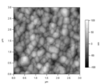
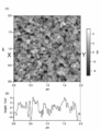
- FIG. 9 is an AFM photograph of the surface of the electrode substrate used in the comparative example.
- FIG. 10 is an AFM photograph of the surface of the electrode substrate used in the example.
- FIG. 11 is an AFM photograph of the surface of the electrode substrate used in the example.
- FIG. 12 is an AFM photograph of the surface of the electrode substrate used in the example.
- FIG. 13 is an AFM photograph of the surface of the electrode substrate used in the example.
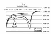
- FIG. 14 is a graph showing a CV curve of the SAM laminate used in the examples.
- FIG. 15 is a graph showing XPS spectra of the SAM laminates used in Examples and Comparative Examples.
- FIG. 16 is a graph showing an XPS spectrum of the SAM laminate used in the example.
- FIG. 17 is a table showing the ratio of detected atoms obtained from the XPS spectra of the SAM laminates used in the examples and comparative examples.
- FIG. 18 is a graph showing the change over time of the surface potential on the electrode substrate surface of the SAM laminate used in the comparative example.
- FIG. 19 is a graph showing the time change of the surface potential on the electrode substrate surface of the SAM laminate used in the example.
- FIG. 20 is a graph showing the potential stability of the surface potential on the electrode substrate surface of the SAM laminate used in the examples and comparative examples.
- the (A) side of FIG. 21 is an AFM photograph of the surface of the electrode substrate used in the example, and the (B) side of FIG. 21 is a curve showing the uneven state of the surface of the electrode substrate used in the example.
- FIG. 22 is a graph showing the potential stability of the surface potential of the electrode substrate used in the example.
- FIG. 23 is a graph showing the potential stability of the surface potential of the electrode substrate used in the example.
- FIG. 24 is a schematic cross-sectional view showing another configuration example of the biomolecule detection electrode chip of the present invention.
- FIG. 25 is a graph showing the surface potential difference of the electrode substrate used in the reference example.
- FIG. 26 is a graph showing the surface potential difference of the electrode substrate used in the reference example.
- FIG. 27 is a graph showing the surface potential difference of the electrode substrate used in the reference example.
- FIG. 28 is an epifluorescence microscope image of the electrode substrate used in the reference example.
- FIG. 29 is an epifluorescence microscope image of the electrode substrate used in the reference example.
- FIG. 30 is an epifluorescence microscope image of the electrode substrate used in the reference example.
- FIG. 31 is a graph showing the change over time of the surface potential of the electrode substrate used in the example.
- FIG. 32 is a bar graph showing the surface potential of the electrode substrate used in the example.
- the electrode chip for biomolecule detection of the present invention includes at least a substrate, an electrode substrate, and a metal salt and a metal oxide provided on the outermost surface of the electrode substrate opposite to the side on which the substrate is provided.
- an electrode having a biomolecular probe immobilization material on which the biomolecular probe provided on the outermost surface is immobilized is configured.
- biomolecules it is known to detect the concentration of biomolecules in a solution as an electrical signal and to quantitatively detect the presence of biomolecules. For example, when an electrode on which a biomolecule probe for capturing a target biomolecule is immobilized is immersed in a solution containing the biomolecule, the biomolecule probe captures the biomolecule and It is known to capture signals.
- a method for capturing an electric signal a current method for capturing the presence of a biomolecule by a change in current and a potential method for capturing by presence of a change in potential are known.
- a current method for example, it is known to use an oxidation-reduction reaction on a metal electrode.
- an oxidizing substance or a reducing substance for example, ascorbic acid
- an electric current based on oxidation or reduction flows, and the detection of biomolecules is hindered, and the detection accuracy may deteriorate. It was.
- an electrode reaction advances on a metal electrode with current measurement. Since the electrode reaction is irreversible and non-equilibrium reaction, corrosion of the metal electrode, generation of gas, and the like occur, and the stability of current measurement is impaired. In particular, the detection accuracy may be deteriorated when repeatedly measuring.
- the above-described biomolecule probe can detect a change in potential at the solid-liquid interface between the electrode and the solution (change in surface charge density) caused by capturing a charged biomolecule.
- a change in potential is detected by a transistor using a field effect.
- metal is generally used as an electrode material, and gold has been conventionally used because it does not cause corrosion due to a solution.
- the potential drift should be suppressed in order to detect the change in potential based on the presence of the biomolecule with high accuracy. That is, by using an electrode material that does not easily polarize and placing the electrode in an environment where the ion concentration in the solution is difficult to increase or decrease, the potential at the solid-liquid interface between the electrode and the solution becomes stable, and potential drift is less likely to occur. Conceivable.
- the electrode chip for biomolecule detection includes a substrate, an electrode substrate, and a metal salt and a metal provided on the outermost surface of the electrode substrate opposite to the side on which the substrate is provided. It is configured to include at least one of oxides and an electrode having a biomolecular probe immobilization material on which a biomolecular probe provided on the outermost surface is immobilized. That is, the electrode material contains at least one of a metal salt and a metal oxide.
- the metal salt is represented as MX
- the metal salt is dissociated into a metal ion (M + ) and a salt ion (X ⁇ ) in an aqueous solution, and is in an equilibrium state as represented by the following formula (1).
- the metal oxide is also dissociated in an aqueous solution to reach an equilibrium state. That is, when the metal oxide is expressed as MO, the metal oxide MO ⁇ is in equilibrium with the hydroxide (MOH) in the aqueous solution, and further becomes MOH 2 + depending on the liquidity (pH) of the aqueous solution. . MO ⁇ , MOH, and MOH 2 + are considered to be in an equilibrium state as shown in the following equation (2).
- the biomolecule detection electrode chip according to the present invention is immersed in an aqueous solution containing X ⁇ ions when it contains a metal salt, and an aqueous solution containing H + ions when it contains a metal oxide, Is in an equilibrium state, and the potential at the solid-liquid interface between the electrode and the solution is considered to be stable. That is, it is considered that potential drift hardly occurs.
- metal salts, metal salts and metal oxides that serve as electrode materials do not cause polarization, and from this point of view, it is considered that potential drift is unlikely to occur. From the above, it is considered that the biomolecule detection electrode chip of the present invention is excellent in potential stability at the solid-liquid interface between the liquid and the electrode.
- the biomolecule detection electrode chip of the present invention having excellent potential stability at the solid-liquid interface between the liquid and the electrode is brought into contact with an aqueous solution containing at least one biomolecule (for example, the chip is immersed in the aqueous solution). If the change in the solid-liquid interface potential of the electrode is detected, the change in potential based on the presence of the biomolecule can be detected more accurately, and the biomolecule can be detected with high accuracy.
- biomolecule detection electrode chip and the biomolecule detection method of the present invention will be described in detail.
- the electrode chip for biomolecule detection of the present invention includes at least a substrate, an electrode substrate, and a metal salt and a metal oxide provided on the outermost surface of the electrode substrate opposite to the side on which the substrate is provided.
- an electrode having a biomolecular probe immobilization material on which the biomolecular probe provided on the outermost surface is immobilized is configured.
- the biomolecule detection electrode chip may further include one or more intermediate layers between the substrate and the electrode.
- the biomolecule detection electrode chip has at least one of a metal salt and a metal oxide on the outermost surface of the electrode
- the metal At least one of the salt and the metal oxide will come into contact with the aqueous solution.
- the metal salt or metal oxide is dissociated, the ions in the aqueous solution are in an equilibrium state, and the potential at the solid-liquid interface between the electrode and the aqueous solution can be stabilized.
- the biomolecule detection electrode chip has a biomolecule probe immobilization material on which the biomolecule probe is immobilized on the outermost surface of the electrode, so that the biomolecule detection electrode chip can be placed in an aqueous solution containing a biomolecule.
- the biomolecular probe comes into contact with the aqueous solution when immersed in the solution.
- the biomolecule probe captures the biomolecule in the aqueous solution, and the change in the potential changed by the charge of the biomolecule can be detected.
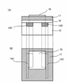
- FIG. 1 shows a biomolecule comprising a substrate 10, an intermediate layer 20 located on the substrate 10 and adjacent to the substrate 10, and an electrode 30 located on the intermediate layer 20 and adjacent to the intermediate layer 20.
- a detection electrode tip 100 is shown.
- the electrode 30 has a metal electrode substrate 32, an inorganic layer 34 composed of at least one of a metal salt and a metal oxide having the electrode substrate 32 as a metal element on the outermost surface of the electrode 30, and a biomolecular probe A biomolecular probe immobilization layer 36 formed using an immobilization material is formed.
- the electrode substrate 32 is covered with the inorganic layer 34 and the biomolecular probe immobilization layer 36 and is not exposed.
- a biomolecule probe 38 is immobilized on the biomolecule probe immobilization layer 36.
- the amount of change in potential detected when the biomolecule detection electrode chip 100 is immersed in an aqueous solution containing biomolecules is measured by a potential measuring device (not shown) connected to the electrode substrate 32 via a lead wire or the like. can do.
- a potential measuring device not shown
- the electrode has at least one of a metal salt and a metal oxide provided on the outermost surface of the electrode substrate opposite to the side on which the substrate is provided. That is, the electrode may include an electrode substrate having only a metal salt on the outermost surface, or may include an electrode substrate having only a metal oxide, or an electrode having both a metal salt and a metal oxide. A substrate may be included.
- the metal salt is not particularly limited.
- silver chloride, calcium chloride, barium chloride, magnesium chloride, zinc chloride, aluminum chloride, calcium nitrate, aluminum sulfate, silver sulfide, silver bromide, silver iodide, platinum chloride, etc. Is mentioned.
- Only one type of metal salt may be used, or two or more types may be used.
- the metal salt is preferably a metal chloride.
- the metal constituting the metal salt is preferably one having good affinity with the biomolecular probe immobilization material described later.
- the metal constituting the metal salt is preferably a metal having a good affinity for a sulfur atom.
- a metal having a good affinity for a sulfur atom Specifically, silver, platinum, Or it is preferable that it is zinc and it is more preferable that it is silver.
- the metal oxide is not particularly limited.
- the metal constituting the metal salt has good affinity with the biomolecular probe immobilization material described later.
- the metal constituting the metal salt is preferably a metal having a good affinity for sulfur atoms.
- tantalum (Ta) Platinum, gold, or titanium is preferable, and tantalum is more preferable.
- the electrode substrate having a metal salt or metal oxide may be an inorganic material such as glass, metal, ITO (Indium Tin Oxide), or an organic material such as polyester or polyolefin.
- the electrode substrate is preferably a metal, and the electrode substrate is composed of a metal or metal oxide constituting the metal salt. More preferably, it is a constituent metal.
- the electrode substrate surface includes at least one of a metal salt and a metal oxide from the viewpoint of the stability of the potential of the solid-liquid interface between the aqueous solution containing biomolecules and the electrode. It is preferable that the inorganic layer is coated with a biomolecular probe immobilization layer formed using a biomolecular probe immobilization material and is not exposed.
- the metal salt or metal oxide only needs to be present on the electrode substrate.
- it may be present as an inorganic layer composed of a metal salt or metal oxide formed on the surface of the electrode substrate.
- a method of forming an inorganic layer composed of a metal salt or metal oxide on the surface of the electrode substrate a method of adhering a separately prepared metal salt or metal oxide on the electrode substrate, a surface of the electrode substrate that is metal And the like, and the like.
- an adhesive such as an epoxy compound is applied to the electrode substrate or metal salt or metal oxide, so that the electrode substrate and the metal salt or metal oxide are oxidized.
- a method of depositing a metal salt or metal oxide on an electrode substrate using an electron beam or the like, or a method of forming by sputtering For example, in order to form a metal oxide layer composed of tantalum oxide on ITO using ITO as an electrode substrate, tantalum oxide may be deposited on the ITO surface. The layer thickness of the tantalum oxide layer can be controlled by adjusting the deposition time.
- Surface treatment of the electrode substrate that is a metal by chemical reaction includes a solution such as a chelating agent solution containing hydrochloric acid, nitric acid, or salt ions, or a gas such as oxygen gas or ozone gas on the surface of the metal electrode substrate.
- a solution such as a chelating agent solution containing hydrochloric acid, nitric acid, or salt ions, or a gas such as oxygen gas or ozone gas on the surface of the metal electrode substrate.
- the method of giving is mentioned.
- the surface of the electrode substrate that is a metal may be surface-treated with a solution that can be used as a target metal salt.
- a chelating agent for example, PDTA; 1,3-Propanediamine Tetraacetic Acid
- Fe 3+ as a ligand
- a chelating agent for example, PDTA; 1,3-Propanediamine Tetraacetic Acid
- the surface of the metal electrode substrate may be oxidized.
- the surface of the metal electrode substrate may be oxidized.
- the electrode substrate may be oxidized by applying a solution containing an oxidizing agent such as hydrogen or spraying oxygen gas, ozone gas, or the like.
- the method for forming the inorganic layer composed of the metal salt on the electrode substrate is preferably a method in which the surface of the electrode substrate that is a metal is surface-treated by a chemical reaction. Moreover, the method of forming the inorganic layer comprised by the metal oxide on the electrode substrate can also vapor-deposit a metal oxide on the surface of the electrode substrate which is a metal.
- the thickness of the inorganic layer including a metal salt or metal oxide is preferably 1 nm to 100 nm, and more preferably 1 nm to 10 nm.
- an inorganic layer composed of a metal salt or a metal oxide on the electrode substrate means that, for example, the surface of the electrode substrate is subjected to AFM (Atomic Force Microscope), TEM (Transmission Electron Microscope). It can be confirmed by photo observation using a microscope such as Transmission (Electron Microscope).
- AFM Atomic Force Microscope
- TEM Transmission Electron Microscope
- Biomolecular probes biomolecular probe immobilization materials
- the electrode has a biomolecular probe immobilization material on which a biomolecular probe provided on the outermost surface of the electrode substrate is immobilized.
- Biomolecular probes include nucleic acids, polynucleotides, synthetic oligonucleotides, antibodies, or antigens. These may be fragments or the like.
- oligonucleotides, cDNA fragments and the like are usually composed of 300 or less bases. When an oligonucleotide is used, it is preferably a nucleic acid fragment having a base length of 80 or less.
- biomolecule probe is bound (immobilized) to the biomolecule probe immobilization material, and specifically binds or reacts with the biomolecule in the aqueous solution containing the biomolecule.
- the biomolecular probe is a single-stranded probe (for example, single-stranded DNA), and after complementary strand binding with the target DNA, a single-base extension reaction that reacts complementarily with the base of the target DNA is used. Specific biomolecules can also be detected with high accuracy. Details of the biomolecule detection method will be described later.
- the biomolecular probe immobilization material is a material for immobilizing the biomolecular probe on the electrode. In order for the electrode to accurately detect the charge of the biomolecule, it is important that the biomolecule probe that captures the biomolecule and the electrode substrate are bound (immobilized).
- biomolecular probe immobilization material examples include a sulfur-containing compound, a silyl group-containing compound, streptavidin (hereinafter also simply referred to as “avidin”), and the like.
- examples of the sulfur-containing compound include alkane thiols and alkane disulfides having an alkyl chain.
- examples of the silyl group-containing compound include alkyl alkoxysilanes having an alkyl chain. Both the sulfur-containing compound and the silyl group-containing compound may be a sulfur-containing compound or a silyl group-containing compound having a polymer chain represented by polyethylene glycol (PEG) instead of the alkyl chain.
- PEG polyethylene glycol
- Sulfur has a high affinity with noble metals such as gold, silver and platinum.
- the salt ion of the metal salt (Cl ⁇ in the case of AgCl) is exposed on the outermost surface of the electrode, and when the metal oxide is present on the outermost surface of the electrode, The metal oxide oxygen ions (O ⁇ ) are exposed on the outermost surface of the electrode.
- salt ions for example, Cl ⁇
- oxygen ions are replaced with sulfur, and the metal and sulfur are bonded.
- the silyl (Si) group has a high affinity with oxygen ions.
- oxygen ions (O ⁇ ) of the metal oxide are exposed on the outermost surface of the electrode.
- a silyl group-containing compound is allowed to act on the oxide of the electrode, oxygen ions (O ⁇ ) and sulfur atoms are bonded.
- a thiol group-containing compound when a thiol group-containing compound is first allowed to act on the metal electrode surface, sulfur is bonded to the metal surface and the thiol group-containing compound is immobilized. Thereafter, when the electrode surface is brought into contact with a reaction solution such as PDTA, a metal salt such as silver chloride is formed on the metal electrode surface where the thiol group-containing compound is not formed.
- a reaction solution such as PDTA
- a metal salt such as silver chloride
- the thickness of the metal salt (silver chloride) layer can be controlled, and the size of the thiol-containing compound, for example, the length of the alkyl group can be controlled.
- the relative position between the functional group (amino group, carboxyl group, aldehyde group, etc.) of the thiol group-containing compound and the metal salt surface, the distance, and the flexibility of the thiol group-containing compound are controlled and optimized. be able to.
- Avidin may be immobilized on the electrode by modifying a part of the molecule with a sulfur-containing compound such as alkanethiol or a silyl group-containing compound such as alkylalkoxysilane.
- a sulfur-containing compound such as alkanethiol or a silyl group-containing compound such as alkylalkoxysilane.
- the binding (immobilization) of the biomolecule probe immobilization material and the biomolecule probe is performed by, for example, modifying either one end of the biomolecule probe or one end of the biomolecule probe immobilization material with an amino group, Is modified with a carboxy group, and the two may be bound by an amide bond or the like.
- the amino group or carboxy group need not be modified.
- the one end may be modified with an aldehyde group and bonded to an amino group.
- biomolecular probe immobilization material is avidin
- biotin having high affinity with avidin Avidin is composed of four subunits, each having a biotin binding site, and thus can bind to four biotins per molecule. Therefore, by modifying biotin at one end of the biomolecule probe, the biomolecule probe immobilization material and the biomolecule probe can be bound (immobilized) using the avidin-biotin bond.
- the biomolecular probe immobilization material is preferably a sulfur-containing compound.
- the sulfur-containing compound functions as a self-assembled membrane (SAM).
- SAM self-assembled film
- SAM refers to a thin film having a structure with a certain order formed by a mechanism of the film material itself without fine control from the outside. This self-organization forms ordered structures and patterns over long distances in a non-equilibrium situation.
- Sulfur-containing compounds such as alkanethiols and alkane disulfides are adsorbed spontaneously on substrates containing noble metals such as noble metals such as gold and silver, metal salts composed of noble metals, and oxides composed of noble metals.
- a monomolecular-sized thin film is given. Therefore, the biomolecule probe can be immobilized on the electrode at a high density, and the detection accuracy of the biomolecule can be further increased.
- a target gene which is a biomolecule to be detected is detected by hybridization with a biomolecule probe (for example, a DNA probe).
- a biomolecule probe for example, a DNA probe.
- the aforementioned biomolecular probe immobilizing material having a hydrophobic group such as alkanethiol is likely to gather due to the interaction of the hydrophobic chain of the alkyl group, resulting in a domain shape.
- Biomolecules such as proteins tend to be adsorbed on a hydrophobic surface, so that they tend to gather and become overcrowded.
- a component having a hydrophilic group such as sulfobetaine (SB) may be mixed with a biomolecular probe immobilization material having a hydrophobic group.
- SBA sulfobetaine
- sulfobetaine is a highly hydrophilic molecule having both a positive charge and a negative charge, it can be mixed with a hydrophobic molecule such as alkanethiol to form a SAM. And hydrophilicity can be adjusted. As a result, it is possible to suppress biomolecular structural damage.
- Specific examples of SB include Sulfobetaine 3-undecanethiol.
- the hydrophobicity and hydrophilicity of the SAM surface can be adjusted by changing the mixing ratio between the hydrophilic component and the biomolecular probe-immobilized material having a hydrophobic group.
- the molar ratio of the DNA probe to sulfobetaine (SB) [DNA probe: SB] is preferably in the range of 1: 1 to 1:10. In order to obtain high hybridization efficiency, 1: 1 is more preferable.
- the DNA probe density on the electrode surface is 0.04 probes / (nm) 2 , that is, 0.04 DNA probes per square nanometer. At this time, the distance between adjacent DNA probes is about 5 nm. Considering that the diameter of the double-stranded DNA is 2 nm, it can be said that the distance between the probes is moderate.
- the DNA probe density is preferably 0.1 probe / (nm) 2 or less.
- a biomolecule probe immobilization material solution in which the biomolecule probe immobilization material is dissolved is applied to the electrode substrate. It may be applied directly or on a layer composed of a metal salt or metal oxide and dried.
- the biomolecule probe may be bonded to the biomolecule probe immobilization material after forming the biomolecule probe immobilization layer.
- the biomolecule probe immobilization material to which the biomolecule probe is bonded is dissolved in a solvent, and the solution is used as an electrode substrate or a metal salt or metal oxide. You may give on the layer comprised by a thing.
- a solution is applied by spin coating, air knife coating, bar coating, blade coating, slide coating, curtain coating, or the like. And a method of applying by a dropping method, a spray method, a vapor deposition method, a casting method, a dipping method, or the like.
- the biomolecule probe immobilization material or the solution in which the biomolecule probe immobilization material bound to the biomolecule probe is dissolved randomly on the electrode substrate or the layer composed of a metal salt or metal oxide. It may be given, arranged in an array, or given in a lump in a domain. Moreover, you may provide in pattern form.
- a solvent for dissolving the biomolecule probe immobilization material or the biomolecule probe immobilization material to which the biomolecule probe is bound water, alcohol, or a mixed solvent thereof is used.
- a water-insoluble organic solvent may be used, but when the biomolecule probe immobilization material to which the biomolecule probe is bound is dissolved, from the viewpoint of handling the biomolecule.
- Water, a water-soluble solvent such as alcohol, or a mixed solvent thereof is used. Among these, water, ethanol, or a mixed solvent thereof is preferable.
- the biomolecular probe can be immobilized on the electrode.
- the biomolecule probe can be immobilized in various shapes such as a pattern and an array by using a solution in which the biomolecule probe immobilization material or the biomolecule probe immobilization material bound to the biomolecule probe is dissolved.
- FIG. 1 shows a state in which the inorganic layer 34 and the biomolecule-immobilized layer 36 are formed in a domain shape. This is because, for example, when the molecules constituting the biomolecule-immobilized layer 36 are hydrophobic, such as an alkyl chain of alkanethiol, they aggregate in a domain by self-organization using a hydrophobic interaction between molecules as a driving force. Therefore, a form as shown in FIG. 1 is formed.
- a pattern structure as shown in FIG. 1 can be artificially formed by a lithography technique.
- the molecules forming the biomolecule-immobilized layer 36 are hydrophilic, such as polyethylene glycol, aggregation between the molecules does not occur. Therefore, the inorganic layer 34 and the biomolecule-immobilized layer 36 can be mixed randomly. it can. This is effective in controlling the distance between the biomolecules and the reaction efficiency when the biomolecule 38 is immobilized on the surface of the biomolecule-immobilized layer 36.
- the size of the biomolecule and the reaction mode are shown in FIG. It is desirable to select such a domain arrangement or a random arrangement.
- the electrode substrate is previously formed in a desired shape, and the biomolecule probe immobilization material or biomolecule probe is bound on the electrode substrate having such a shape.
- An embodiment in which a solution in which the probe immobilization material is dissolved may be applied.
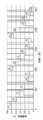
- FIG. 2 shows a laminate 200 in which a patterned electrode substrate 130 is provided on a glass substrate 110.
- the (A) side of FIG. 2 is a schematic top view of the stacked body 200
- the (B) side of FIG. 2 is a schematic side view of the stacked body 200.
- 2A includes an electrode substrate 130 in which a rectangular electrode substrate 130a and a circular electrode substrate 130c are connected to each other on a glass substrate 110 by a linear electrode substrate 130b. It is shown.
- the same reference numerals are used on the (A) side in FIG.
- a layer composed of a metal salt or a metal oxide and a biomolecule probe immobilization layer on which a biomolecule probe is immobilized are formed on a circular electrode substrate 130c, and the linear electrode substrate 130b is used as a wiring.
- a potential of a biomolecule can be detected by connecting a potential measuring device to the rectangular electrode substrate 130a.
- a resist for example, Nippon Kayaku Co., Ltd., SU-8 may be applied.
- FIG. 3 shows a laminate 202 in which a resist is provided on the laminate 200 shown in FIG.
- the (A) side in FIG. 3 is a schematic top view of the laminate 202
- the (B) side in FIG. 3 is an alternate long and short dash line connecting the X and Y shown in FIG. It is a side surface schematic diagram of the laminated body 202 in-).
- a layer made of a metal salt or metal oxide can be formed by applying a solution for surface treatment such as hydrochloric acid to the exposed circular electrode substrate 130c.
- a biomolecule probe immobilization layer on which the biomolecule probe is immobilized is formed by applying a solution in which the biomolecule probe immobilization material bonded with the biomolecule probe is applied to the exposed circular electrode substrate 130c. be able to.
- the fact that the biomolecular probe immobilization material is immobilized on the electrode substrate means that, for example, X-ray photoelectron spectroscopy such as XPS (X-ray Photoelectron Spectroscopy) or ESCA (Electron Spectroscopy for Chemical Analysis) is performed on the electrode substrate surface. This can be confirmed by performing an analysis. For example, when alkanethiol is used as the biomolecular probe immobilization material, a peak derived from a sulfur atom is detected when the alkanethiol is immobilized on the electrode substrate. In addition, it can be confirmed that the biomolecule probe is immobilized on the biomolecule probe immobilization material, for example, by labeling the biomolecule with a fluorescent molecule and performing fluorescence detection.
- the biomolecule detection electrode chip includes a substrate for supporting the electrode substrate.
- the substrate is not particularly limited, and may be an inorganic material typified by a glass substrate, an ITO substrate, a metal substrate, or the like, or an organic material typified by a polyester substrate, a polyolefin substrate, or the like.
- a semiconductor provided with an electronic device such as a field effect transistor (FET) may be used as the substrate.
- FET field effect transistor
- one or more intermediate layers may be provided between the substrate and the electrode substrate.
- the intermediate layer can be a functional layer such as an adhesive layer for improving the adhesion between the substrate and the electrode substrate.
- an adhesive layer it is preferable to use a material having good affinity with both the substrate and the electrode substrate.
- Ti titanium
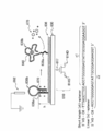
- FIG. 4 shows a schematic diagram of a floating gate type FET
- FIG. 5 shows a schematic diagram of an extended type FET. 4 and 5, the (A) side is a cross-sectional view, and the (B) side is a top view.
- a floating gate type FET (hereinafter referred to as “F-FET”) is shown.
- the F-FET is formed on the silicon substrate 12, the drain 14D and the source 14S which are provided on the silicon substrate 12, and on the silicon substrate 12, the drain 14D and the source 14S.
- a floating electrode 18 is formed on a channel region between the drain 14D and the source 14S, and the potential is detected by the floating electrode 18. Therefore, in the F-FET, the channel region between the drain 14D and the source 14S is located in the region vertically below the floating electrode 18, as shown on the (B) side in FIG.
- an extended FET (hereinafter referred to as “E-FET”) is shown on the (A) side of FIG.
- the E-FET is formed on the silicon substrate 12, the drain 14D and the source 14S which are provided on the silicon substrate 12, and on the silicon substrate 12, the drain 14D and the source 14S.
- an extraction electrode 15 is provided inside the insulating film 16.
- the channel region between the drain 14D and the source 14S is not located in the region below the floating electrode 18, and the region below the floating electrode 18 is vertically below.
- One end of the extraction electrode 15 is located in the region.
- a channel region between the drain 14D and the source 14S is located in a region vertically below the other end of the extraction electrode 15.
- the gate insulating film 16 includes silicon oxide (SiO 2 ), silicon nitride (SiN), aluminum oxide (Al 2 O 3 ), A material such as tantalum oxide (Ta 2 O 5 ) is used singly or in combination, and in order to keep the transistor operation normally, silicon nitride (SiN), aluminum oxide (Al 2 O 3 ) on silicon oxide (SiO 2 ). ) Or tantalum oxide (Ta 2 O 5 ).
- the gate electrode 17 is preferably polysilicon (Poly-Si), and has good consistency with a so-called self-alignment process in which the source 14S and the drain 14D are formed by ion implantation through the polysilicon gate.
- the floating electrode 18 is preferably made of a material having a high affinity with the electrode substrate, and a noble metal such as gold, platinum, silver, or palladium can be used.
- the extraction electrode 15 is used as a wiring, a material with low resistance and good workability such as etching is preferable.
- a material with low resistance and good workability such as etching is preferable.
- the material polysilicon (Poly-Si), aluminum, molybdenum, or the like can be used.
- the extraction electrode 15 and the floating electrode 18 can be formed of the same material such as gold.
- the biomolecule detection method of the present invention includes a substrate, an electrode substrate, and at least one of a metal salt and a metal oxide provided on the outermost surface of the electrode substrate opposite to the side on which the substrate is provided,
- a biomolecule detection electrode chip provided with an electrode having a biomolecule probe immobilization material on which the biomolecule probe provided on the outermost surface is immobilized is brought into contact with an aqueous solution containing at least one kind of biomolecule. It has an aqueous solution contact step and a detection step for detecting a change in the solid-liquid interface potential of the electrode.
- the biomolecule detection method of the present invention comprises an aqueous solution contact step in which the biomolecule detection electrode chip of the present invention described above is contacted with an aqueous solution containing at least one biomolecule, and a solid-liquid interface potential of the electrode. And a detecting step for detecting a change in the above.
- the biomolecule detection electrode chip of the present invention is brought into contact with an aqueous solution containing at least one kind of biomolecule (hereinafter also referred to as “biomolecule aqueous solution”).
- biomolecule aqueous solution a method in which at least one of a metal salt and a metal oxide provided in an electrode chip for biomolecule detection, and a biomolecule probe immobilized on a biomolecule probe immobilization material are in contact with an aqueous solution. If it is, it will not be restrict
- the outermost surface of the electrode of the biomolecule detection electrode chip is immersed in the biomolecule aqueous solution, or the biomolecule aqueous solution is dropped on the outermost surface of the electrode of the biomolecule detection electrode chip, or the biomolecule detection is performed in the biomolecule aqueous solution.
- the electrode tip for use may be immersed.
- the potential of the solid-liquid interface between the electrode and the aqueous solution is stabilized by at least one of the metal salt and the metal oxide included in the biomolecule detection electrode chip of the present invention.
- the biomolecule probe immobilized on the biomolecule probe immobilization material included in the biomolecule detection electrode chip of the present invention captures the biomolecule in the aqueous solution and the solid-liquid interface generated by the capture of the biomolecule. By detecting the change in potential, the presence of a biomolecule can be quantitatively detected.
- the biomolecule probe is a DNA probe having a base sequence complementary to the target gene
- an appropriate reaction condition is applied.
- the target gene and the DNA probe form a complementary complex [Hybridization].
- the biomolecule probe captures the biomolecule.
- Detection process a change in the solid-liquid interface potential between the electrode provided in the biomolecule detection electrode chip and the biomolecule aqueous solution or the detection solution is detected.
- Biomolecules in the aqueous biomolecule solution are positively charged or negatively charged.
- the aqueous biomolecule solution is generally prepared in a buffer solution (buffer solution) having a pH of 7-8. Under such a pH environment, DNA is negatively charged.
- the charged nucleic acid forms a complex by hybridization with the DNA probe, which is a biomolecule probe, so that the charge density changes at the solid-liquid interface between the electrode and the biomolecule aqueous solution, and the surface potential changes. To do.
- a cleaning step of cleaning the biomolecule detection electrode tip with a cleaning liquid may be incorporated before the inspection step.
- the washing liquid is not particularly limited as long as it is a liquid that can remove the aqueous biological component solution attached to the biomolecule detection electrode chip, and examples thereof include water, a phosphate buffer solution, an aqueous NaCl solution, and physiological saline.
- the biomolecule detection electrode chip of the present invention After bringing the biomolecule detection electrode chip of the present invention into contact with the biomolecule aqueous solution, the biomolecule detection electrode chip is washed with a cleaning liquid, and other biomolecules or interference other than the target adsorbed nonspecifically on the electrode chip By removing the components, highly accurate measurement can be performed.
- a solution for detecting a potential change at the solid / liquid interface of the electrode is introduced onto the surface of the electrode chip.
- An electric double layer is formed at the solid / liquid interface, and the potential change at the solid / liquid interface depends on the electric double layer.
- the width (thickness) of the electric double layer is called a Debye length, which is a function of ionic strength.
- the Debye length is small in a solution with a high salt concentration, for example, about 1 nm in a NaCl solution of 100 mmol / L (hereinafter also referred to as mM).
- the Debye length increases in the diluted solution, for example, about 10 nm in a 1 mmol / L NaCl solution.
- the Debye length is long.After washing and removing the aqueous solution of the biological component adhering to the biomolecule detection electrode chip, it is replaced with a detection solution with an optimized concentration and fixed. It is desirable to measure the potential change at the / liquid interface.
- a phosphate buffer solution having a concentration of 1 mmol / L to 10 mmol / L is applied to an electrode tip on a metal oxide surface, and 1 mmol / L to 10 mmol / L is applied to an electrode tip on a metal salt surface such as silver chloride.
- a sodium chloride aqueous solution or a potassium chloride aqueous solution having a concentration can be used.
- Such a change in potential is measured by a potential measuring device connected to the electrode.
- the potential measuring device include an electrometer manufactured by Keithley.
- the change in the surface potential of the electrode may be measured by the FET described above.
- the change in the surface potential has the same effect as the change in the gate voltage of the FET, and changes the conductivity of the channel.
- the drain current flowing between the source and the drain the formation of a complex by hybridization, that is, the presence of the target gene can be detected.
- FIG. 6 is a schematic diagram showing a configuration example of a measurement system in the biomolecule detection method of the present invention.
- the measurement system shown in FIG. 6 uses a biomolecule detection electrode chip and a reference chip to perform differential measurement using two chips.
- FIG. 6 shows a part of a biomolecule detection electrode chip including an electrode configured using the electrode substrate 333a and a reference chip configured using the electrode substrate 333b.
- the electrode substrates 333a and 333b are both made of silver and supported by a glass substrate (not shown).
- a part of the surface of the electrode substrate 333a is surface-treated to have a silver chloride layer (inorganic layer), and the biomolecule-immobilizing material 336a is immobilized on the remaining surface. Chloride ions (Cl ⁇ ) 334a are exposed on the surface of the silver chloride layer.
- the biomolecule immobilization material 336a is immobilized on the electrode substrate 333a via sulfur (S). Further, the biomolecule immobilization material 336a immobilizes the biomolecule probe 338. Therefore, the electrode composed of the electrode substrate 333a has a biomolecule-immobilized layer composed of a silver chloride layer and a biomolecule-immobilized material 336a on which the biomolecule probe 338 is immobilized on the outermost surface. .
- the electrode composed of the electrode substrate 333b has a silver chloride layer and a biomolecule-immobilized layer composed of the biomolecule-immobilized material 336a formed on the outermost surface.
- each electrode is in contact with the aqueous biomolecule solution 370. That is, the biomolecule-immobilized layer composed of the biomolecule-immobilizing material 336a on which the silver chloride layer and the biomolecule probe 338 are immobilized on the electrode substrate 333a, and the silver chloride layer and the biomolecule on the electrode substrate 333b.
- a biomolecule-immobilized layer composed of the molecule-immobilized material 336b is immersed in the biomolecule aqueous solution 370.
- the reference electrode 362 is also immersed in the biomolecule aqueous solution 370.
- the electrode substrates 333a and 333b are connected to operational amplifiers 364a and 364b, the operational amplifiers 364a and 364b are connected to the operational amplifier 366, and the operational amplifier 366 is connected to the differential amplification output 368. ing.
- the biomolecule detection electrode chip including the electrode substrate 333a measures the surface potential using the operational amplifier 364a
- the reference chip including the electrode substrate 333b measures the surface potential using the operational amplifier 364b.
- Each surface potential measurement signal is input to a differential amplification output 368 via an operational amplifier 366.
- the biomolecule detection electrode chip and the reference chip have the same electrical characteristics, it is desirable to use a pair of chips integrated on the same substrate.
- the reference chip can be used in common, and the difference between a different biomolecule detection electrode chip and a common reference chip can be used. Measure.
- FIG. 7 shows a schematic diagram of a reaction showing an example of a single-base extension reaction of a nucleic acid in the biomolecule detection method of the present invention.
- 7A to 7E are an electrode substrate 432, an oligonucleotide probe 437 that is a single-stranded DNA probe immobilized on the electrode substrate 432, and a target for detecting a gene sequence.
- Target DNA 440 is shown.
- Oligonucleotide probe 437 which is a single-stranded DNA probe immobilized on electrode substrate 432, is immersed in a biomolecule aqueous solution (nucleic acid aqueous solution) containing nucleic acid, and target DNA 440 is contained in the nucleic acid aqueous solution. It is a nucleic acid.
- the electrode substrate 432 is a part of the biomolecule detection electrode chip of the present invention described above, and a layer (inorganic layer) composed of a metal salt or metal oxide is also formed on the surface of the electrode substrate 432.
- configurations other than the electrode substrate 432 and the oligonucleotide probe 437 are not shown in the (A) to (E) portions of FIG.
- the oligonucleotide probe 437 captures the target DNA 440, and a part of the target DNA 440 and the oligonucleotide probe 437 form a complex by hybridization. That is, a part of the base of the target DNA 440 and the base of the oligonucleotide probe 437 are complementarily bonded.
- the base sequence (target base sequence) 440a that does not form a complex with the oligonucleotide probe 437 can be grasped by a single base extension reaction of DNA.
- bases such as adenine (A), thymine (T), guanine (G), and cytosine (C) possessed by nucleic acids react with a specific base in a complementary manner and form a pair.
- A adenine
- T thymine
- G guanine
- C cytosine
- Target DNA 440 TCTATATGCACGGTCCACCTC Oligonucleotide probe 437: AGATATACCGTG
- the electrode substrate 432 side to TCTATATGGCAC form a complex, and the base of the base sequence consisting of GGTCCACCTC (target base sequence 440a) is not paired.
- a base that forms a complex by hybridization in the target base sequence 440a.
- dATP deoxyadenosine 5'-triphosphate
- base G which reacts complementarily with base C DGTP (deoxyguanosine 5′-triphosphate) which can be introduced into nucleic acid
- dTTP deoxythymidine 5′-triphosphate
- DNA has a negative charge, and a negative charge is detected each time one base pair is formed. Therefore, it is possible to determine the number of complementary reactions, that is, the number of bases that have formed a complex by hybridization, from the magnitude of the detected change in surface potential. Since base G shows a complementary reaction only with base C, dATP, dGTP, dTTP, etc., which are deoxynucleotides other than dCTP, are introduced into the aqueous nucleic acid solution under the situation shown in part (A) of FIG. Even so, no single-base extension reaction occurs. Therefore, under the situation shown in part (A) of FIG.
- hybridization occurs only when dCTP is introduced, and the surface potential of the electrode changes, resulting in a change in surface potential and a change in surface potential. From the type of deoxynucleotide, the number and type of bases of the target base sequence 440a can be detected.
- the base adjacent to the base (base G) in the target base sequence forming a complex by hybridization is the base T. Therefore, under the situation shown in FIG. 7B, the surface potential of the electrode changes only when dATP is added to the aqueous nucleic acid solution, and the number of bases T can be determined from the amount of potential change. . As shown in part (C) of FIG. 7, there is only one base pair generated by the introduction of dATP.
- an electrode chip for biomolecule detection immersed in an aqueous solution containing DNA polymerase and deoxynucleotides in another aqueous solution containing different types of DNA polymerase and deoxynucleotides, it contains other different types of DNA polymerase and deoxynucleotides. It is preferable to immerse at least the electrode of the biomolecule detection electrode chip after washing with water, a buffer solution or the like before reimmersing in the aqueous solution.
- the dissociation equilibrium of the metal oxide shown in the above-described formula (2) moves according to the hydrogen ion concentration, and the electrode potential is accordingly changed. Since it changes, it becomes a good pH sensor. Therefore, an electrode tip having a metal oxide on its surface is effective in detecting hydrogen ions released as a result of the elongation reaction.
- the oligonucleotide probe 437 which is a single-stranded nucleic acid, is reacted with one base by sequentially reacting dGTP and dTTP. Each of them is extended to form a complex sequentially with the target DNA 440 which is the target nucleic acid. If the surface potential of the electrode does not change regardless of which DNA polymerase is inserted, this means that the base sequence of the target DNA has been analyzed, and the analysis is completed.
- biomolecule detection electrode chip provided with a hairpin aptamer probe and a biomolecule detection method using the same>
- an electrode chip for biomolecule detection provided with a hairpin aptamer probe using an intercalator and ATP (adenosine triphosphate)
- a target biomolecule can be detected with high accuracy.
- the biomolecule detection electrode chip provided with the hairpin aptamer probe is the biomolecule detection electrode described above except that the biomolecule probe provided in the biomolecule detection electrode chip of the present invention is in the form of a hairpin aptamer probe. It is the same as the electrode tip configuration.
- the surface of the electrode substrate on which the biomolecular probe is immobilized has at least one of a metal salt and a metal oxide, the potential stability at the solid-liquid interface between the liquid and the electrode is excellent. Of course, the same.
- the hairpin aptamer probe can induce a large signal by changing the structure upon target recognition in the presence of a reporter molecule (intercalator).
- a reporter molecule intercalator
- an electronic transistor such as an FET as the substrate that constitutes the electrode chip
- the bio-responsible response to external stimuli from biochemical sources is achieved by utilizing the transistor's characteristics such as switching and amplification of specific electrical signals. It is expected to realize a new class of base information processing devices. Details of the biomolecule detection electrode chip provided with the hairpin aptamer probe will be described with reference to FIG.
- FIG. 24 shows a biomolecule detection provided with a hairpin aptamer probe composed of an extended gate FET substrate 610, an electrode substrate 630, a biomolecule probe immobilization material layer 636, and a hairpin aptamer probe 638 (biomolecule probe).
- An electrode tip, an ATP 640, an intercalator 670, and a reference electrode 662 are shown.
- the FET substrate 610, the electrode substrate 630, and the biomolecule probe immobilization material layer 636 are laminated in this order, and the hairpin aptamer probe 638 is immobilized on the biomolecule probe immobilization material layer 636 as a biomolecule probe.
- the FET substrate 610 includes a drain electrode 614D, a source electrode 614S, and a gate electrode 617. By connecting the gate electrode 617 to the electrode substrate 630, a potential change that has changed on the electrode substrate 630 can be obtained.
- the substrate 610 senses.
- the biomolecule probe immobilization material layer 636 is a layer in which the aforementioned biomolecule probe immobilization material is bonded to the electrode substrate 610.
- a dense self-assembled monolayer SAM
- SAM dense self-assembled monolayer
- MCH 6-mercapto-1-hexanol
- a hairpin aptamer probe 638 capable of binding to ATP640 as a biomolecule probe is immobilized on the biomolecule probe immobilization material layer 636.
- the hairpin aptamer probe 638 includes a compound (hereinafter referred to as a specific probe compound) including a structural site 638a capable of forming a structure that can easily enter the intercalator 670 and a structural site 638b including an adenosine 5′-triphosphate (ATP) binding sequence. Also called).
- a structural site having an ATP binding sequence actively binds to ATP and does not react with, for example, GTP (guanosine triphosphate).
- two hairpin aptamer probes 638 are shown.
- One is shown on the left side of FIG. 24 as a short hairpin aptamer probe (sh-aptamer) in which the structural site 638b is a closed loop, and the other is the structural site 638b opened on the right side of FIG. It is shown as a linear aptamer probe in a loop (ln-aptamer).
- sh-aptamer short hairpin aptamer probe
- ln-aptamer probe refers to a biomolecule probe of a biomolecule detection electrode chip equipped with a hairpin aptamer probe, and conformation of both sh-aptamer conformation and ln-aptamer conformation. Shall be included.
- the sh-aptamer is a conformation of a specific probe compound molecule when the structural site 638b containing the ATP binding sequence does not capture ATP, and the ln-aptamer captures the ATP by the structural site 638b containing the ATP binding sequence. This is the conformation of the specific probe compound molecule.
- the structural site 638a forms a layered molecular structure and has a structure in which an intercalator easily enters between layers.
- the structural site 638a in the sh-aptamer is also referred to as “stem”.
- the intercalator is positively charged and has a structure that is linked to the sh-aptamer structural site 638a by electrostatic interaction, ⁇ - ⁇ interaction, or the like.
- the intercalator is represented by DAPI having the following structure.
- a compound is used.
- the hairpin aptamer probe has a positive charge.
- the size of the structural site 638a of the sh-aptamer is preferably 3 nm or less (h ⁇ 3 nm) including the size of the SAM.
- the conformation of the specific probe compound molecule is changed, the structural site 638b containing the ATP binding sequence is opened, and the hairpin aptamer probe 638 captures ATP640. Further, when the structural portion 638b is opened, the intercalator 670 is released from the hairpin aptamer probe 638, and the hairpin aptamer probe 638 loses a positive charge.
- a biomolecule can be recognized by a method without a label using a DNA binding species.
- FIG. 24 shows an example of the structure of specific probe compound molecules constituting the sh-aptamer and ln-aptamer. Note that the structural formula shown in FIG. 24 is a state in which an alkanethiol having 6 carbon atoms and a specific probe compound molecule are bound to each other at the top and bottom, and the 37-mer base sequence site excluding “HS-C6-” It becomes the structure of a specific probe compound molecule.
- C6 refers to an alkyl chain having 6 carbon atoms and represents a part of alkanethiol.
- the c1 portion of the sh-aptamer shown by the 27mer base sequence and the c2 portion of the ln-aptamer correspond to the structural site 638b of the specific probe compound molecule (hairpin aptamer probe 638), which is an ATP binding sequence.
- the sh-aptamer forms a pair when the underlined 7-mer base reacts in a complementary manner, and constitutes a part of the structural site 638a.
- the amount of positive charge lost by the hairpin aptamer probe 638 changing from the sh-aptamer structure to the ln-aptamer structure is converted into a potential difference signal by the field effect of the FET.
- the buffer concentration controls the screening of ions for potential analysis. Real-time measurement of the interfacial potential can be performed with dilution buffer (DPBS is pH 7.4, 15 mM Dulbecco's phosphate buffered saline).
- the difference between the sh-aptamer conformation and the ln-aptamer conformation can be determined by identifying the conformation using an epifluorescence microscope.
- Conformational identification uses indicator dyes (also referred to as fluorescent labels, fluorescent probes, etc.) such as TO-PRO-3.
- the indicator dye may be a known one such as a product manufactured by Beckman-Coulter.
- Biomolecule detection electrode chips 1 and 4 (Examples 1 and 3 respectively) provided with electrodes having AgCl as a metal salt on the metal electrode substrate, and metal salts and metal oxides on the metal electrode substrate
- a biomolecule detection electrode chip 101 (Comparative Example 1) having an electrode from which the metal of the metal electrode substrate was exposed was prepared.
- the metal salt to produce a metal oxide and a Ta 2 O 5 for biomolecules detected with an electrode having an electrode tip 2 (Example 2) on the metal electrodes on the substrate.
- the prescription for producing each biomolecule detection electrode chip is as follows.
- a silver (Ag) plate having a thickness of 90 nm and a surface dimension of 5 mm ⁇ 5 mm was prepared as a metal electrode substrate.
- a glass substrate having a thickness of 1 mm and having the same surface dimensions as the electrode substrate was prepared.
- a titanium (Ti) plate having a thickness of 10 nm and the same surface dimensions as the electrode substrate was prepared. The prepared silver plate, titanium plate, and glass substrate were laminated in this order and bonded to produce an electrode substrate laminate A.
- Electrode substrate laminates A Five prepared electrode substrate laminates A were prepared. Among them, the electrode substrate surfaces of the four electrode substrate laminates A were respectively immersed in the chelate solutions 1 and 2 prepared as described below and dried to obtain surface-treated electrode substrate laminates 1 to 4. .
- Surface treatment electrode substrate laminates 1 and 2 have a contact time between the silver plate and chelate solution 1 of 20 seconds, and surface treatment electrode substrate laminate 3 has a contact time between the silver plate and chelate solution 2 of 180 seconds, In the surface-treated electrode substrate laminate 4, the contact time between the silver plate and the chelate solution 2 was 300 seconds. After each contact time, the surface of each surface-treated electrode substrate was washed with water.
- the surface-treated electrode substrate laminate 1 was prepared by previously immersing the electrode substrate laminate A in a 100 mM NaCl aqueous solution and then adding a 100 mM PDTA ⁇ Fe (III) aqueous solution to start the reaction.
- the surface-treated electrode substrate laminate 2 was prepared by first immersing the electrode substrate laminate A in a 100 mM PDTA ⁇ Fe (III) aqueous solution and then dipping it in a 100 mM NaCl aqueous solution to start the reaction. is there.
- the contact time shown in Table 1 represents the contact time of the PDTA ⁇ Fe (III) aqueous solution.
- SAM laminate Six surface-treated electrode substrate laminates 1 are prepared, and the following SAM-forming solutions 1 to 5 are applied to each of the five electrode substrate surfaces, and a laminate in which SAM is laminated on the electrode substrate laminate (hereinafter “ Also referred to as “SAM laminate”.
- FIG. 8 is a schematic cross-sectional view of the SAM laminate 500, and the SAM laminate 500 includes an electrode substrate laminate 580.
- the SAM laminate 500 includes an electrode substrate laminate 580.
- a glass substrate 510, a titanium plate intermediate layer 520, and a silver plate electrode substrate 532 are laminated in this order.
- a silver chloride layer 534 made of silver chloride (AgCl) and a self-assembled film SAM 536 are formed on the electrode substrate 532 of the electrode substrate laminate 580.
- the silver chloride layer 534 has two regions, and the self-assembled film SAM 536 has three regions.
- a SAM formation comparison solution was applied to the electrode substrate surface of the surface-treated electrode substrate laminate 1 to obtain a comparative laminate 201.
- the details of the preparation formulations of the SAM formation solutions 1 to 5 and the SAM formation comparison solution are as follows.
- Table 3 shows the coating configurations of the SAM laminates 1 to 5 and the comparative laminate 201. Moreover, the coating structure of the SAM laminated body 101 and the SAM laminated body 102 for a comparison mentioned later is also shown.
- the biomolecule probe is formed by allowing the carboxy group of the self-assembled film SAM of the SAM laminate 1 produced as described above to act as an oligonucleotide having an amino group at the 5 ′ end, which is a biomolecule probe, to form an amide bond.
- the biomolecule detection electrode chip 1 of Example 1 was produced.
- the biomolecular probe is immobilized on the self-assembled film SAM in the same manner except that the SAM laminate 101 is used instead of the SAM laminate 1 as the SAM laminate. did. As described above, the biomolecule detection electrode chip 101 of Comparative Example 1 was produced.
- a SAM laminate 102 was fabricated as a comparative SAM laminate.
- the SAM laminate 102 is an electrode substrate laminate A that is not subjected to surface treatment instead of using the surface-treated electrode substrate laminate 1 as an electrode substrate laminate.
- a self-assembled film SAM was formed on the electrode substrate in the same manner except that was used.
- the SAM laminated body 102 which is a comparative self-assembled film SAM-containing electrode substrate laminated body was produced.
- Types of SAM laminates and SAM concentrations used in biomolecule detection electrode chip 1 and biomolecule detection electrode chip 101, and types of surface treatment of electrode substrate laminate A used in the preparation of SAM laminates Table 4 summarizes the surface morphology ("surface species" column).
- FIGS. 9 to 13 show the results of formation of metal salt layer.
- FIG. 9 is an AFM photograph of the electrode substrate surface of the electrode substrate laminate A, that is, the surface of the silver plate.
- FIGS. 10 to 13 show the electrode substrate surface and the silver chloride of the surface-treated electrode substrate laminates 1 to 4, respectively. It is an AFM photograph of the layer surface. In the photograph shown in FIG. 9, no white area is observed, but in FIGS.
- a white area is observed.
- Such a white region is considered to be AgCl, and the area of the white region increases as the sodium chloride concentration increases and the contact time between the silver plate and the chelate solution increases, and AgCl is formed on the silver plate.
- the vertical and horizontal axes of the AFM photographs shown in FIGS. 9 to 13 indicate the size of the observation region, and the unit is [ ⁇ m].
- the band-shaped scale located on the right side of the AFM photograph indicates the size of the irregularities on the surface of the electrode substrate or the surface of the silver chloride layer, and the numerical values are given according to the gradation from white to black.
- the unit of the band-shaped scale is [nm].
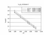
- the vertical axis represents current [A] and the horizontal axis represents potential [V].
- a curved line A indicated by a solid line and a curved line B indicated by a broken line show the CV characteristics of two electrode chips produced under the same conditions. Both the curve A and the curve B have two minimum peaks in the lower curve that appears when the potential is swept in the positive direction. Among these, a small peak shown in the vicinity of ⁇ 1100 [V] indicates the presence of Ag—S bonds in the SAM laminate.
- the horizontal axis of the XPS spectrum indicates the binding energy [eV], and the vertical axis indicates the number of photoelectrons [c / s (counts / sec)].
- Each of the SAM laminates 1, 3, 5 and the comparative laminate 201 uses the surface-treated electrode substrate laminate 1 in which the surface of the electrode substrate laminate A is surface-treated with a chelate solution as the electrode substrate laminate. Therefore, silver chloride is formed on the surface of the surface-treated electrode substrate laminate 1.
- the XPS spectrum shown in FIG. 15 shows the abundance of chlorine atoms (Cl) contained in the silver electrode surfaces of the SAM laminates 1, 3, 5 and the comparative laminate 201. The higher the amount, the greater the peak height.
- the curve A of the SAM laminate 1 having a large SAM concentration has a low peak indicating the abundance of chlorine atoms, and the peak increases as the SAM concentration decreases. It has become. This is because as the SAM concentration increases, the number of sulfur bound to the silver surface increases, and the proportion of the area occupied by the SAM in the substrate surface increases. Since the silver chloride layer is formed by chemical treatment after the SAM is formed, the silver chloride layer is formed in the remaining portion where the SAM is not formed. Therefore, the SAM concentration dependency as shown in FIG. 15 is observed.
- the SAM laminates 1, 3, 5 are obtained by applying a SAM forming solution having a SAM concentration shown in Table 5 to the surface-treated electrode substrate laminate 1.
- the SAM formation solution contains alkanethiol (a biomolecule probe solidifying material) having a sulfur atom.
- the comparative laminate 201 is obtained by applying a SAM formation comparison solution containing no alkanethiol and having a SAM concentration of 0 ⁇ mol / L to the surface-treated electrode substrate laminate 1.
- the XPS spectrum shown in FIG. 16 shows curves AC having peaks indicating the presence of sulfur atoms (S) contained in the SAM laminates 1, 3, and 5, and the laminate 201 For, no curve with peaks was obtained.
- the curve A of the SAM laminate 1 with a high SAM concentration has a higher peak, and the peak is lower as the SAM concentration is lower. This is because as the SAM concentration increases, the number of sulfur bonded to the silver surface increases, and the proportion of the area occupied by the SAM in the substrate surface increases.
- the table shown in FIG. 17 shows the ratio of detected atoms obtained from the XPS spectra shown in FIGS.
- the unit of each numerical value is [%].
- Atoms detected by XPS analysis include carbon atoms (C), chlorine atoms (Cl), oxygen atoms (O), and sulfur atoms (S). It is considered that the carbon atom is derived from the hydrocarbon chain of alkanethiol constituting the self-assembled film SAM, and the sulfur atom is derived from the thiol of alkanethiol.
- the chlorine atom is considered to be derived from chloride ions in the silver chloride layer.
- oxygen atoms are derived from moisture in the air attached to the electrode substrate.
- “1 ⁇ M”, “5 ⁇ M”, and “10 ⁇ M” in the Sample column are the concentrations of the SAM forming solution when forming the SAM laminate.
- bare Ag in the Sample column is a laminate obtained by using the surface-treated electrode substrate laminate 1 in which the AgCl surface is exposed without forming the SAM. Represents the body 201.
- bare Ag the slight detection of the presence of carbon atoms is considered to be derived from ethanol constituting the SAM formation comparison solution applied to the surface-treated electrode substrate laminate 1.
- the stability of the surface potential on the electrode substrate surface was evaluated.
- the SAM laminate 4 and the SAM laminate 102 are both produced using the SAM forming solution 4 having a SAM concentration of 3 ⁇ mol / L.
- the electrode substrate laminate to which the SAM forming solution 4 is applied is subjected to surface treatment in the SAM laminate 4 to form AgCl, and the SAM laminate 102 is not subjected to surface treatment and the Ag plate is exposed. .
- the surface potential was measured by using a 6514 type electrometer manufactured by Keithley as a potential measuring device, and using sodium / silver chloride reference electrodes immersed in a saturated potassium chloride solution as a standard, sodium chloride having a concentration of 2.5 mM, 25 mM, and 250 mM. The solution was used. The results are shown in FIGS.
- FIG. 18 shows changes over time in the surface potentials on the electrode substrate surface of six identical SAM laminates 4 produced using the surface-treated electrode substrate laminate 1 having a silver chloride layer formed on the electrode substrate surface (A1 to A6). ).
- FIG. 19 shows the time variation (B1 to B8) of the surface potential on the electrode substrate surface of eight identical SAM laminates 102 produced using the electrode substrate laminate A with the silver plate exposed on the electrode substrate surface. It is a graph. In both FIG. 18 and FIG. 19, the vertical axis represents the surface potential [V], and the horizontal axis represents the elapsed time [second]. The surface potential is measured by replacing the solution soaked with 25 mM sodium chloride and alternately with 250 mM sodium chloride.
- the SAM laminate 4 in which the silver chloride layer is formed on the electrode substrate surface has a stable surface potential in 5 to 200 seconds, often about 30 seconds from the start of measurement of the surface potential. ing.
- the surface potential is not stable and potential drift occurs.
- FIG. 20 a graph showing variations in the surface potential of the SAM laminate 4 and the SAM laminate 102 is shown in FIG.
- the vertical axis represents the surface potential [V] on the electrode substrate surface of the SAM laminate
- the horizontal axis represents the concentration [mol / L] of sodium chloride (NaCl) used for the measurement.
- the curve A representing the surface potential of the SAM laminate 4 having a silver chloride layer on the electrode substrate has a small length of the vertical bar indicating the variation in the surface potential, and the potential stability of the surface potential. Is excellent. This is presumably because the silver chloride of the silver chloride layer formed on the electrode substrate is dissociated and is in an equilibrium state in the aqueous solution.
- the curve B representing the surface potential of the SAM laminate 102 formed by using the electrode substrate on which the silver plate is exposed has a large vertical bar indicating the variation in the surface potential, and the surface potential is It turns out that it is not stable.
- the surface potential changes according to the sodium chloride concentration of the immersed solution, and the larger the sodium chloride concentration, the smaller the surface potential itself and the smaller the surface potential variation.
- the electrode potential has a negative slope with respect to the anion (chlorine ion) and is proportional to the logarithm of the ion concentration. From FIG. 20, the electrode having silver chloride formed on the surface has good linearity with respect to the logarithm of the chlorine ion concentration, and the surface potential based on the electrochemical equilibrium described by the Nernst equation is obtained. It is possible to control the surface potential.
- an electrode with silver exposed on the surface shows a non-linear response, and it is assumed that the surface potential is changed by other mechanisms such as physical adsorption of ions.
- a self-assembled film SAM was formed on the silver surface by allowing alkanethiol having a carboxyl terminus dissolved in ethyl alcohol to act on the surface of the electrode chip where silver was exposed at a concentration of 1 ⁇ mol / L ( ⁇ M). Thereafter, the electrode tip was immersed in a mixed solution of 100 mM 1,3-diaminopropanetetraacetic acid / iron / ammonium / monohydrate [PDTA / Fe (III)] and 100 mM sodium chloride (NaCl) for 20 seconds, Silver chloride was formed on the surface of the silver where no SAM was formed.
- an amide bond is formed between the amino group on the electrode surface and the carboxyl group of the oligonucleotide, thereby Immobilized on the electrode surface.
- the electrode potential changed about 10 mV in the negative direction. This is presumably because the target DNA having a negative charge formed a complementary strand bond with the oligonucleotide on the electrode surface. As described above, it was confirmed that the target DNA can be detected with the biomolecule detection electrode chip of the present invention.
- Electrode substrate laminate As an electrode substrate, an ITO substrate having a thickness of 100 nm and a surface dimension of 5 mm ⁇ 5 mm was prepared. As a substrate for supporting the electrode substrate, a glass substrate having a thickness of 1 mm and having the same surface dimensions as the electrode substrate was prepared. The prepared ITO substrate and a glass plate were adhered to produce an electrode substrate laminate T for the biomolecule detection electrode chip 2.
- Electrode substrate laminates T are prepared, and the surface of the electrode substrate is subjected to electron beam evaporation using tantalum oxide (Ta 2 O 5 ), and a metal oxide layer containing a deposited film with a thickness of 20 nm is contained. An electrode substrate laminate 5 was obtained.
- the biomolecule probe was immobilized in the same manner except that the SAM laminate 1 was used instead of the SAM laminate 1 as the SAM laminate.
- enzyme urease was used as a biomolecule.
- the biomolecule detection electrode tip 2 of Example 2 was produced. Table 7 shows the configuration of the SAM laminate 6 used in the biomolecule detection electrode chip 2.
- the vertical axis indicates the size of the surface unevenness [nm]
- the horizontal axis indicates the AFM.
- the same observation area size [ ⁇ m] as the horizontal axis of the photograph is shown.
- the horizontal axis of the AFM photograph shown on the (A) side and the horizontal axis shown on the (B) side are shown in correspondence with each other. From FIG. 21, the average roughness R RMS of the tantalum oxide layer surface was 1.855 nm, and it was found that a uniform and flat film was obtained.
- aqueous solutions having six different pH values of pH 1.68, pH 4.01, pH 6.86, pH 7.41, pH 9.18, and pH 10.1 were prepared.
- the metal oxide layer-containing electrode substrate laminate 5 was immersed in each of the prepared liquid aqueous solutions, and the change over time in the surface potential of the surface of the metal oxide layer-containing electrode substrate laminate 5 was measured for about 100 seconds immediately after the immersion. .
- the metal oxide layer-containing electrode substrate laminate 5 has an aqueous solution of pH 1.68, an aqueous solution of pH 4.01, an aqueous solution of pH 6.86, an aqueous solution of pH 7.41, an aqueous solution of pH 9.18, and an aqueous solution of pH 10.1.
- the soaking was repeated 3 times.
- the metal oxide layer-containing electrode substrate laminate 5 is taken out of the aqueous solution and immersed in the next aqueous solution, the metal oxide layer-containing electrode substrate laminate 5 is washed with water and dried, and then the next aqueous solution is used. Soaked in.
- the variation in surface potential on the surface of each metal oxide layer when the metal oxide layer-containing electrode substrate laminate 5 was placed in various pH environments was evaluated.
- the surface potential measurement was performed by connecting the metal oxide layer-containing electrode substrate laminate 5 to a 6514 type electrometer manufactured by Keithley, based on a silver-silver chloride reference electrode.
- FIG. 22 The measurement results are shown in FIG. In FIG. 22, the vertical axis represents the surface potential [V] and the horizontal axis the time change [second].
- A1 to a3 shown above the arrows ( ⁇ ) represent changes in surface potential in an aqueous solution at pH 1.68
- b1 to b3 represent changes in surface potential in an aqueous solution at pH 4.01
- c1 to c3 Represents the change in the surface potential in the aqueous solution at pH 6.86
- d1 to d3 represent the change in the surface potential in the aqueous solution at pH 7.41
- e1 to e3 represent the surface potential in the aqueous solution at pH 9.18.
- F1 to f3 represent changes in the surface potential in an aqueous solution with a pH of 10.1.
- a straight line A in FIG. 23 is a regression line of the surface potential plotted against the pH of a1 to f1 in FIG. 22, and a straight line B is a regression line of the surface potential plotted against the pH of a2 to f2 in FIG.
- a straight line C is a regression line obtained by plotting the surface potential with respect to pH of a3 to f3 in FIG.
- FIG. 23 shows that a good linear response is exhibited in a wide pH range from pH 1.68 to pH 10.1.
- the slopes of the regression lines A to C shown in FIG. 23 are referred to as slope sensitivity and serve as an index for evaluating the performance as a metal oxide film material and a pH sensor.
- the relationship between the surface potential and pH is expressed by the Nernst equation. According to this, the slope sensitivity is about 58 mV / pH at room temperature.
- the slopes of the three regression lines shown in FIG. 23 are ⁇ 0.052 V / pH, ⁇ 0.050 V / pH, and ⁇ 0.051 V / pH, respectively, and the reproducibility and uniformity are good.
- urea was detected according to the following prescription.
- Urea is an important biochemical component in evaluating renal function. Urea is decomposed as shown in the following formula (3) by the catalytic action of the enzyme urease.
- the aqueous solution hydrogen ion concentration that is, pH changes. Therefore, the urea concentration as the measurement target can be known by measuring the pH change.
- the surface potential of the electrode chip changed about 15 mV in 1 minute after introduction. This is because urease immobilized on the electrode surface reacts with urea in the solution to be measured, and hydrogen ions are consumed according to the formula (3). It is thought that it was possible to detect with the oxide electrode.
- the SAM forming solution 6 was prepared by using 6-Carboxy-1-decanthiol instead of using 10-Carboxy-1-decanthiol as the biomolecular probe immobilization material. -Prepared similarly except using Mercapto-1-hexanol (MCH).
- MCH Mercapto-1-hexanol
- a probe compound having a 37-mer base sequence shown as an example of the sh-aptamer structure in FIG. 24 was prepared.
- the hairpin aptamer probe was immobilized on the SAM laminate 6 by allowing the carboxyl group of the probe compound to act on the hydroxy group of the self-assembled film SAM of the SAM laminate 6 to form an ester bond.
- the biomolecule detection electrode chip 3 was produced.
- the hairpin aptamer probe provided in the biomolecule detection electrode tip 3 immersed in the DPBS dilution buffer does not contain ATP in the DPBS dilution buffer before the addition of the ATP aqueous solution. It is thought that he is taking a formation.
- DAPI aqueous solution containing DAPI (intercalator) was added to a container in which biomolecule detection electrode chip 3 (sh-aptamer) was immersed in a DPBS dilution buffer. Thereafter, an ATP aqueous solution was added, and the potential difference when the ATP aqueous solution was added was measured. Next, after washing the biomolecule detection electrode chip 3 with the DPBS dilution buffer, a container in which the biomolecule detection electrode chip 3 (sh-aptamer) is immersed in the DPBS dilution buffer is prepared separately, and the DAPI aqueous solution is stored in the container. Added to. Thereafter, an aqueous solution of GTP was added, and the potential difference when the aqueous solution of GTP was added was measured. The results are shown in FIG.
- the carboxy group of the probe compound having the ln aptamer structure shown in FIG. 24 was allowed to act on the hydroxy group of the self-assembled film SAM of the SAM laminate 6 in the same manner.
- the biomolecule detection electrode chip 4 in which the ln aptamer was immobilized on the SAM laminate 6 was produced.
- the potential measurement 1 when the ATP aqueous solution was added in the same manner except that the obtained biomolecule detection electrode tip 4 (In aptamer) was used instead of the biomolecule detection electrode tip 3 (sh-aptamer) And the potential difference when the GTP aqueous solution was added were measured. The results are shown in FIG.
- the linear (ln) aptamer Since the linear (ln) aptamer has an ATP binding sequence, it has a function of capturing the target ATP, but the electrode connected to the ln aptamer could not detect ATP (FIG. 27). This is thought to be due to the fact that ATP is electrically neutral in the DPBS dilution buffer at pH 7.4, so that no significant signal is generated by detection of ATP using the FET. Conceivable. Therefore, both the sh-aptamer setting and DAPI need to generate a measurement signal.
- FET devices can convert the intrinsic charge of molecules in the electric double layer.
- the characteristic device cleaning length of the solution can be described as a function of ionic strength (I) as ( ⁇ ) ⁇ ⁇ I 1/2 .
- the Debye length calculated in 15 mM DPBS dilution buffer was 2.5 nm. This corresponds to an intramolecular distance of only 7 mer at the 5 ′ end of the sh-aptamer within the Debye length when converted from the base base length (0.34 nm).
- FET devices are believed to respond sensitively only to stem charge changes due to DAPI dissociation upon capture of a particular ATP.
- FIG. 28 shows an epifluorescent image of the surface (AgCl surface) of the electrode substrate on which the SAM and hairpin aptamer probe are not formed
- FIG. 29 shows a state before ATP is allowed to act on the biomolecule detection electrode chip 3 (sh-aptamer).
- FIG. 30 shows an epifluorescent image after ATP was allowed to act on the biomolecule detection electrode chip 3 (sh-aptamer).
- FIG. 29 shows that the hairpin aptamer probe had a closed-loop sh-aptamer conformation.
- FIG. 30 showing the system in the presence of ATP, fluorescence emission is not observed, and the hairpin aptamer probe has a conformation different from that of the sh-aptamer, that is, the conformation of the ln-aptamer. Recognize.
- An FET is a powerful transducer for detecting ions and charged particles as a potential difference signal in an unlabeled manner. Also, the expanded gate structure configuration facilitates sensor chip changes in a cost effective manner. However, high sensitivity detection of weakly charged or uncharged analytes has been a major issue.
- the use of structured oligonucleotide aptamer probes of molecular recognition elements in combination with groove binding or intercalating species can expand the use of FET sensors to detect a wide variety of neutral molecules. In the future, DAPI can be improved by improving the safety of the assay and using a DNA binder with less carcinogenicity.
- the critical signal induced by the release of the charge indicator from the electrical double layer at the gate solution nanointerface overcomes the potential drawback of ion screening for analytes charged to FET biosensing Is expected to do.
- Each approach described in the present invention may be detected using a target-specific sh-aptamer in combination with the built-in charge of the shield and a large molecular cationic groove binder.
- DAPI cationic indicator
- the large change obtained as a potentiometric signal was induced by the dissociation of preloaded DAPI from target-induced self-denaturation and the hairpin trunk of the electric double layer by the formation of aptamer and ATP complexes.
- the structured aptamer concept allows FET biosensors to detect neutral analytes with minimal impact from the length of device cleaning.
- the hairpin aptamer combined with the function of the FET is expected to play a role as a general switch for transmitting ATP recognition to an electric signal.
- Electrode substrate laminate C in which a glass substrate, a titanium film, and a silver film were laminated in this order was produced in the following manner.
- a synthetic quartz glass substrate having a thickness of 1 mm and a size of 100 mm ⁇ 100 mm was prepared.
- the surface of the synthetic quartz glass substrate was cleaned by (1) reverse sputtering, (2) a titanium (Ti) film was deposited by vapor deposition, and (3) silver (Ag) was further formed on the obtained Ti film.
- a film was formed by vapor deposition. The Ti film was formed to improve the adhesion between the synthetic quartz glass substrate and the Ag film.
- the Ti film of the electrode substrate laminate C was 10 nm thick, and the Ag film was 90 nm thick.
- the sputtering conditions (1) to (3) are as follows.
- As the sputtering apparatus a sputtering apparatus “Jsputter” was used.
- SAM-forming solution 7 containing 10-Carboxy-1-decanthiol (10-CDT) (Dojindo Laboratories) and Sulfobetaine 3-undecanethiol (SB) into the electrode substrate surface of the electrode substrate laminate C, A SAM laminate 7 was formed on the electrode substrate surface.
- the SAM-forming solution 7 was prepared in the same manner as the SAM-forming solution 1 except that Sulfobetaine 3-undecanethiol was further mixed.
- a chelate solution (chelate solution 1) containing PDTA ⁇ Fe (III) (Cylest Killest PD-FN Sample) (PDTA ferric ammonium complex) is applied to the electrode substrate surface of the produced SAM laminate 7, A silver chloride layer was formed.
- chelate solution 1 containing PDTA ⁇ Fe (III) Cylest Killest PD-FN Sample
- PDTA ferric ammonium complex is applied to the electrode substrate surface of the produced SAM laminate 7, A silver chloride layer was formed.
- substrate laminated body 6 which contains SAM containing SB and silver chloride on the surface was obtained.
- an oligonucleotide having an amino group at the 5 ′ end which is a biomolecule probe (DNA probe) was allowed to act on the carboxy group of the self-assembled membrane SAM to form an amide bond, thereby immobilizing the biomolecule probe.
- the biomolecule detection electrode chip 4 of Example 3 was produced.
- the SAM contains hydrophobic 10-Carboxy-1-decanthiol and hydrophilic sulfobetaine 3-undecanethiol (SB)
- all the ends of the SAM are biomolecule probes.
- a part is a biomolecular probe and a part is SB.
- the molar ratio of DNA probe to SB [DNA probe: SB] is 1: 1 and 0.04 probe / (nm) 2 .
- the metal salt layer-containing electrode substrate laminate 6 is the electrode substrate having the pattern shown in FIGS. 2 and 3 described above, and has 10 circular electrode substrates on the surface (the electrode substrates in FIGS. 2 and 3). 130c) and a rectangular electrode substrate (corresponding to the electrode substrate 130a in FIGS. 2 and 3). Each of the circular electrode substrates has a diameter of 500 ⁇ m.
- the SAM containing SB formed in the above process and the silver chloride layer are formed.
- the circular electrode substrate and the rectangular electrode substrate are connected by a linear electrode substrate 130b as shown in FIGS.
- a glass cylinder that surrounds all of the 10 circular electrode substrates and can be disposed outside the enclosure is disposed on the surface of the metal salt layer-containing electrode substrate laminate 6,
- the cylinder was glued so as not to leak water to form a cylindrical container having a bottom surface with a surface having ten circular electrode substrates.
- the biomolecule detection electrode chip 4 comes into contact with the 10 circular electrode substrates and does not come into contact with the rectangular electrode substrate. It has a configuration.
- control sample which is the sample (2)
- the target sample which is sample (3), is a liquid obtained by diluting a PCR product (PCR products) containing microRNA-143 amplified by adding microRNA-143 to the PCR buffer and performing 30 thermal cycles. is there.
- Each sample of (1), (2), and (3) was dropped onto the circular electrode substrate in the cylindrical container of the biomolecule detection electrode chip 4 at the time interval shown in FIG. Specifically, the sample (1) in FIG. 31 (1), the sample (2) in (2) in FIG. 31, and the sample (3) in (3) in FIG. 31 are dropped three times on the electrode substrate. Each sample was contacted. In addition, the surface potential of each electrode substrate was read at time points (A) and (B) in FIG. The reading of the surface potential at time (A) was performed after dropping the sample (2) (control sample) onto the electrode substrate and washing the electrode with a buffer. Further, the reading of the surface potential at the time (B) was performed after dropping the sample (3) (target sample) onto the electrode substrate and washing the electrode with a buffer. The results are shown in FIG. 31 and FIG.
- FIG. 31 is a graph showing the temporal change of the surface potential in the evaluation of the stability of the surface potential of the biomolecule detection electrode tip 4.
- the electrode chip for biomolecule detection since the surface potential settles immediately after the addition of each sample of (1), (2), and (3), and the baseline is hardly changed, the electrode chip for biomolecule detection It can be seen that if the electrode substrate of 4 is used, stable surface potential difference measurement can be performed. Since the biomolecule detection electrode chip 4 has ten circular electrode substrates capable of detecting biomolecules, the surface potential due to biomolecule adsorption was measured on each of the ten electrode substrates. FIG. 31 shows one of the data, but the same tendency was observed in the other nine electrode substrates.
- FIG. 32 is a bar graph showing the average of surface potentials read at (A) time point and (B)) in FIG.
- the surface potential of the control sample that is, the PCR buffer is read
- the surface potential of the target sample is read.
- the bar graph shown on the left (C) is the surface potential when the control sample (Control) is brought into contact with the electrode substrate
- the bar graph shown on the right (T) shows the target sample including the target as an electrode. The surface potential when brought into contact with the substrate.
- the bar graph of FIG. 32 also shows an error bar indicating measurement variation.
- the sizes of the error bars shown in (C) and (T) are both about 1 mV, indicating that the variation is small.
- a small error bar indicates that the surface potential is stable.
- Electrode substrate 34 Inorganic layer (metal salt and metal At least one of the oxides) 36: Biomolecule probe immobilization layer 38: Biomolecule probe 100: Biomolecule detection electrode chip 110: Glass substrate 130: Electrode substrate 130a: Rectangular electrode substrate 130b: Linear electrode substrate 130c: Circular electrode substrate 200 : Laminate 202: laminate 333a: electrode substrate 333b: electrode substrate 334a: part of metal salt 334b: part of metal salt 336a: biomolecular probe immobilization material 336b: biomolecule probe immobilization material 338: biomolecule probe 362: reference electrode 364a: operational amplifier 364b: operational amplifier 366: operational amplifier 368: differential amplification output 370: aqueous biomolecule solution 432: electrode substrate 437: oligonucle
Abstract
Description
遺伝子の機能及び発現解析を大規模に行い、遺伝子検査へ発展させる技術は、既に、DNAチップまたはDNAマイクロアレイとして、市販されている。しかし、現状のDNAチップ及びDNAマイクロアレイの多くは、蛍光物質などの標識分子を用いて、光学的に生体分子を検出する蛍光検出を基本原理としているため、レーザや複雑な光学系が必要となり、システムが大型化し高価である。 In recent years, the decoding of genome base sequences of various organisms including the human genome has progressed rapidly, and a large amount of base sequence information is being accumulated. By clarifying the functions of genes in living organisms, it is expected that the development of gene-related technologies will progress dramatically in a wide range of fields such as diagnosis of various diseases, development of pharmaceuticals, and improvement of crop varieties. In the development of such gene-related technologies, it is important to analyze base sequence information and gene expression and function information with high accuracy.
A technique for conducting gene function and expression analysis on a large scale and developing it to genetic testing is already commercially available as a DNA chip or a DNA microarray. However, many of the current DNA chips and DNA microarrays are based on the principle of fluorescence detection that optically detects biomolecules using a labeling molecule such as a fluorescent substance. Therefore, a laser and a complicated optical system are required. The system is large and expensive.
特開2005-077210号公報に記載の方式によれば、低コストで、酸化還元反応を用いた生体分子の検出方法に比べ、精度の高い検出方法ではあるが、安定した電位が得られにくく、より高い水準の精度が求められていた。 However, the method described in Nature Biotechnology, vol. 16, (1998) p27, p40 uses the oxidation-reduction reaction on the metal electrode as the basic principle of detection, so that an oxidizing substance or a reducing substance (for example, ascorbic acid) is contained in the sample. ), An electric current based on oxidation or reduction flows, which may interfere with gene detection and may deteriorate detection accuracy. In addition, the electrode reaction easily proceeds on the metal electrode along with the current measurement. Furthermore, since the electrode reaction is irreversible and non-equilibrium reaction, electrode corrosion, gas generation, etc. may occur, and the stability of current measurement may be impaired, especially when repeated measurement is performed, the detection accuracy deteriorates. was there.
According to the method described in JP-A-2005-072210, although it is a low-cost and highly accurate detection method compared to a biomolecule detection method using an oxidation-reduction reaction, it is difficult to obtain a stable potential, A higher level of accuracy was required.
<1> 基板と、電極基板、及び、前記電極基板の前記基板が設けられている側とは反対側の最表面に設けられた金属塩および金属酸化物の少なくとも一方、並びに、前記最表面に設けられた生体分子プローブが固定化された生体分子プローブ固定化材料を有する電極とを備える生体分子検出用電極チップである。 Specific means for achieving the above object are as follows.
<1> A substrate, an electrode substrate, and at least one of a metal salt and a metal oxide provided on the outermost surface opposite to the side on which the substrate is provided, and the outermost surface. An electrode chip for biomolecule detection comprising an electrode having a biomolecule probe immobilization material on which a provided biomolecule probe is immobilized.
生体分子検出用電極チップを上記構成とすることで、液体と電極との固液界面(固/液界面とも表現される)における電位の安定性に優れた生体分子検出用電極チップとすることができる。 The electrode chip for biomolecule detection of the present invention includes at least a substrate, an electrode substrate, and a metal salt and a metal oxide provided on the outermost surface of the electrode substrate opposite to the side on which the substrate is provided. On the other hand, an electrode having a biomolecular probe immobilization material on which the biomolecular probe provided on the outermost surface is immobilized is configured.
By configuring the biomolecule detection electrode chip as described above, it is possible to obtain a biomolecule detection electrode chip having excellent potential stability at a solid-liquid interface (also expressed as a solid / liquid interface) between a liquid and an electrode. it can.
電流方式としては、例えば、金属電極上での酸化還元反応を利用することが知られている。しかし、生体分子を含む溶液中に、酸化物質または還元物質(例えば、アスコルビン酸)が存在すると、酸化または還元に基づく電流が流れ、生体分子の検出が妨げられ、検出精度が劣化することがあった。また、電流計測に伴い、金属電極上で電極反応が進行する。電極反応は不可逆で非平衡反応であるため、金属電極の腐食、ガスの生成等が生じ、電流測定の安定性が損なわれ、特に繰返し測定する場合に検出精度が劣化することがあった。 Regarding the detection of biomolecules, it is known to detect the concentration of biomolecules in a solution as an electrical signal and to quantitatively detect the presence of biomolecules. For example, when an electrode on which a biomolecule probe for capturing a target biomolecule is immobilized is immersed in a solution containing the biomolecule, the biomolecule probe captures the biomolecule and It is known to capture signals. As a method for capturing an electric signal, a current method for capturing the presence of a biomolecule by a change in current and a potential method for capturing by presence of a change in potential are known.
As a current method, for example, it is known to use an oxidation-reduction reaction on a metal electrode. However, if an oxidizing substance or a reducing substance (for example, ascorbic acid) is present in a solution containing biomolecules, an electric current based on oxidation or reduction flows, and the detection of biomolecules is hindered, and the detection accuracy may deteriorate. It was. Moreover, an electrode reaction advances on a metal electrode with current measurement. Since the electrode reaction is irreversible and non-equilibrium reaction, corrosion of the metal electrode, generation of gas, and the like occur, and the stability of current measurement is impaired. In particular, the detection accuracy may be deteriorated when repeatedly measuring.
さらに、電極材料として、一般に金属が用いられるところ、溶液による腐食が生じないとの理由から、従来は、金が用いられていた。しかし、金は分極を起こすため、固液界面の電位が安定せず、生体分子の存在に基づく電位の変化を、精度良く検出することができなかった。このように電位が不安定になること(「電位ドリフト」とも称する)は、電極が浸されている溶液中のイオン濃度が増減することによっても生ずる。 On the other hand, as a potential method, the above-described biomolecule probe can detect a change in potential at the solid-liquid interface between the electrode and the solution (change in surface charge density) caused by capturing a charged biomolecule. Are known. According to the method described in Japanese Patent Application Laid-Open No. 2005-077210, it is known that such a change in potential is detected by a transistor using a field effect. However, if a transistor is used, equipment for manufacturing a semiconductor is required, and it is difficult to meet the demand for cost reduction.
Furthermore, metal is generally used as an electrode material, and gold has been conventionally used because it does not cause corrosion due to a solution. However, since gold is polarized, the electric potential at the solid-liquid interface is not stable, and the change in electric potential based on the presence of biomolecules cannot be detected with high accuracy. Such potential instability (also referred to as “potential drift”) also occurs when the concentration of ions in the solution in which the electrode is immersed increases or decreases.
金属塩をMXと表すと、金属塩は、水溶液中で、金属イオン(M+)と塩イオン(X-)とに解離し、下記式(1)に示す式のごとく平衡状態になる。 Here, the electrode chip for biomolecule detection according to the present invention includes a substrate, an electrode substrate, and a metal salt and a metal provided on the outermost surface of the electrode substrate opposite to the side on which the substrate is provided. It is configured to include at least one of oxides and an electrode having a biomolecular probe immobilization material on which a biomolecular probe provided on the outermost surface is immobilized. That is, the electrode material contains at least one of a metal salt and a metal oxide.
When the metal salt is represented as MX, the metal salt is dissociated into a metal ion (M + ) and a salt ion (X − ) in an aqueous solution, and is in an equilibrium state as represented by the following formula (1).
以上より、本発明の生体分子検出用電極チップは、液体と電極との固液界面における電位の安定性に優れると考えられる。 Therefore, the biomolecule detection electrode chip according to the present invention is immersed in an aqueous solution containing X − ions when it contains a metal salt, and an aqueous solution containing H + ions when it contains a metal oxide, Is in an equilibrium state, and the potential at the solid-liquid interface between the electrode and the solution is considered to be stable. That is, it is considered that potential drift hardly occurs. In addition, unlike metal salts, metal salts and metal oxides that serve as electrode materials do not cause polarization, and from this point of view, it is considered that potential drift is unlikely to occur.
From the above, it is considered that the biomolecule detection electrode chip of the present invention is excellent in potential stability at the solid-liquid interface between the liquid and the electrode.
本発明の生体分子検出用電極チップは、基板と、電極基板、及び、前記電極基板の前記基板が設けられている側とは反対側の最表面に設けられた金属塩および金属酸化物の少なくとも一方、並びに、前記最表面に設けられた生体分子プローブが固定化された生体分子プローブ固定化材料を有する電極とを備えて構成される。
生体分子検出用電極チップは、さらに、基板と、電極との間に、1層以上の中間層を備えていてもよい。 <Electrode chip for biomolecule detection>
The electrode chip for biomolecule detection of the present invention includes at least a substrate, an electrode substrate, and a metal salt and a metal oxide provided on the outermost surface of the electrode substrate opposite to the side on which the substrate is provided. On the other hand, an electrode having a biomolecular probe immobilization material on which the biomolecular probe provided on the outermost surface is immobilized is configured.
The biomolecule detection electrode chip may further include one or more intermediate layers between the substrate and the electrode.
また、生体分子検出用電極チップが、電極の最表面に、生体分子プローブが固定化された生体分子プローブ固定化材料を有することで、生体分子検出用電極チップを、生体分子を含有する水溶液中に浸したときに、生体分子プローブが水溶液と接触することになる。これによって、生体分子プローブが水溶液中の生体分子を捕捉し、生体分子が有する電荷によって変化した電位の変化を検出することができる。 When the biomolecule detection electrode chip has at least one of a metal salt and a metal oxide on the outermost surface of the electrode, when the electrode chip for biomolecule detection is immersed in an aqueous solution containing a biomolecule, the metal At least one of the salt and the metal oxide will come into contact with the aqueous solution. As a result, the metal salt or metal oxide is dissociated, the ions in the aqueous solution are in an equilibrium state, and the potential at the solid-liquid interface between the electrode and the aqueous solution can be stabilized.
Further, the biomolecule detection electrode chip has a biomolecule probe immobilization material on which the biomolecule probe is immobilized on the outermost surface of the electrode, so that the biomolecule detection electrode chip can be placed in an aqueous solution containing a biomolecule. The biomolecular probe comes into contact with the aqueous solution when immersed in the solution. As a result, the biomolecule probe captures the biomolecule in the aqueous solution, and the change in the potential changed by the charge of the biomolecule can be detected.
図1には、基板10と、基板10の上に位置し、基板10と隣接する中間層20と、中間層20の上に位置し、中間層20と隣接する電極30とを備えた生体分子検出用電極チップ100が示されている。電極30は、金属の電極基板32を有し、電極30の最表面に、電極基板32を金属要素とする金属塩及び金属酸化物の少なくとも一方で構成された無機層34、並びに、生体分子プローブ固定化材料を用いて構成される生体分子プローブ固定化層36が形成されている。電極基板32は、無機層34と生体分子プローブ固定化層36とで覆われ、露出していない。また、生体分子プローブ固定化層36には、生体分子プローブ38が固定化されている。
生体分子検出用電極チップ100を、生体分子を含有する水溶液中に浸したときに検出される電位の変化量は、電極基板32とリード線等を介して連結された図示しない電位測定器により測定することができる。
以下、符号を省略して説明する。 A configuration example of the biomolecule detection electrode chip of the present invention will be described with reference to FIG.
FIG. 1 shows a biomolecule comprising a
The amount of change in potential detected when the biomolecule
Hereinafter, description will be made with the reference numerals omitted.
(金属塩、金属酸化物)
電極は、電極基板の前記基板が設けられている側とは反対側の最表面に設けられた金属塩および金属酸化物の少なくとも一方を有する。
すなわち、電極は、最表面に金属塩のみを有する電極基板を含んでいてもよいし、金属酸化物のみを有する電極基板を含んでいてもよいし、金属塩および金属酸化物の両方を有する電極基板を含んでいてもよい。 〔electrode〕
(Metal salt, metal oxide)
The electrode has at least one of a metal salt and a metal oxide provided on the outermost surface of the electrode substrate opposite to the side on which the substrate is provided.
That is, the electrode may include an electrode substrate having only a metal salt on the outermost surface, or may include an electrode substrate having only a metal oxide, or an electrode having both a metal salt and a metal oxide. A substrate may be included.
以上の中でも、血清等の生体分子を含有する水溶液は、塩化物イオンを多く含むことから、金属塩は、金属塩化物であることが好ましい。また、金属塩を構成する金属は、後述する生体分子プローブ固定化材料との親和性が良いものが好ましい。生体分子プローブ固定化材料として、例えば、アルカンチオールを用いる場合には、金属塩を構成する金属が、硫黄原子との親和性が良い金属であることが好ましく、具体的には、銀、白金、または亜鉛であることが好ましく、銀であることがより好ましい。 The metal salt is not particularly limited. For example, silver chloride, calcium chloride, barium chloride, magnesium chloride, zinc chloride, aluminum chloride, calcium nitrate, aluminum sulfate, silver sulfide, silver bromide, silver iodide, platinum chloride, etc. Is mentioned. Only one type of metal salt may be used, or two or more types may be used.
Among these, since the aqueous solution containing biomolecules such as serum contains a large amount of chloride ions, the metal salt is preferably a metal chloride. Further, the metal constituting the metal salt is preferably one having good affinity with the biomolecular probe immobilization material described later. For example, when using alkanethiol as the biomolecular probe immobilization material, the metal constituting the metal salt is preferably a metal having a good affinity for a sulfur atom. Specifically, silver, platinum, Or it is preferable that it is zinc and it is more preferable that it is silver.
以上の中でも、金属塩を構成する金属が、後述する生体分子プローブ固定化材料との親和性が良いものが好ましい。生体分子プローブ固定化材料として、例えば、アルカンチオールを用いる場合には、金属塩を構成する金属が、硫黄原子との親和性が良い金属であることが好ましく、具体的には、タンタル(Ta)、白金、金、またはチタンであることが好ましく、タンタルであることがより好ましい。 The metal oxide is not particularly limited. For example, tantalum oxide (Ta 2 O 5 ), titanium oxide (TiO 2 ), aluminum oxide (Al 2 O 3 ), magnesium oxide (MgO 2 ), zinc oxide (ZnO) 2 ), silicon oxide, tin oxide, platinum oxide, gold oxide and the like. Only one type of metal oxide may be used, or two or more types may be used.
Among the above, it is preferable that the metal constituting the metal salt has good affinity with the biomolecular probe immobilization material described later. For example, when alkanethiol is used as the biomolecular probe immobilization material, the metal constituting the metal salt is preferably a metal having a good affinity for sulfur atoms. Specifically, tantalum (Ta) Platinum, gold, or titanium is preferable, and tantalum is more preferable.
金属塩ないし金属酸化物で構成される無機層を、後述する表面処理により形成する場合には、電極基板は金属であることが好ましく、電極基板は、金属塩を構成する金属または金属酸化物を構成する金属であることがより好ましい。
ただし、電極基板が金属である場合は、生体分子を含む水溶液と電極との固液界面の電位の安定性の観点から、電極基板表面は、金属塩および金属酸化物の少なくとも一方を含んで構成される無機層と、生体分子プローブ固定化材料を用いて構成される生体分子プローブ固定化層とで被覆され、露出していないことが好ましい。 The electrode substrate having a metal salt or metal oxide may be an inorganic material such as glass, metal, ITO (Indium Tin Oxide), or an organic material such as polyester or polyolefin.
When the inorganic layer composed of a metal salt or metal oxide is formed by the surface treatment described later, the electrode substrate is preferably a metal, and the electrode substrate is composed of a metal or metal oxide constituting the metal salt. More preferably, it is a constituent metal.
However, when the electrode substrate is a metal, the electrode substrate surface includes at least one of a metal salt and a metal oxide from the viewpoint of the stability of the potential of the solid-liquid interface between the aqueous solution containing biomolecules and the electrode. It is preferable that the inorganic layer is coated with a biomolecular probe immobilization layer formed using a biomolecular probe immobilization material and is not exposed.
例えば、ITOを電極基板とし、ITO上にタンタル酸化物で構成された金属酸化物層を形成するには、ITO表面にタンタル酸化物を蒸着すればよい。蒸着時間を調整することにより、タンタル酸化物層の層厚を制御することができる。 As a method of adhering a separately prepared metal salt or metal oxide on the substrate, an adhesive such as an epoxy compound is applied to the electrode substrate or metal salt or metal oxide, so that the electrode substrate and the metal salt or metal oxide are oxidized. And a method of depositing a metal salt or metal oxide on an electrode substrate using an electron beam or the like, or a method of forming by sputtering.
For example, in order to form a metal oxide layer composed of tantalum oxide on ITO using ITO as an electrode substrate, tantalum oxide may be deposited on the ITO surface. The layer thickness of the tantalum oxide layer can be controlled by adjusting the deposition time.
金属である電極基板の表面に、金属塩で構成される無機層を形成するためには、金属である電極基板の表面を、目的の金属塩とし得る溶液等で表面処理すればよい。例えば、銀板表面に塩化銀で構成された層を形成するには、銀板表面に、Fe3+を配位子とするキレート剤(例えば、PDTA;1,3-Propanediamine Tetraacetic Acid)に塩化ナトリウムを溶解したキレート溶液を付与すればよい。キレート溶液中の塩化ナトリウムの濃度を調整したり、キレート溶液と銀板との接触時間を調整することにより、無機層たる塩化銀層の層厚を制御することができる。 Surface treatment of the electrode substrate that is a metal by chemical reaction includes a solution such as a chelating agent solution containing hydrochloric acid, nitric acid, or salt ions, or a gas such as oxygen gas or ozone gas on the surface of the metal electrode substrate. The method of giving is mentioned.
In order to form an inorganic layer composed of a metal salt on the surface of the electrode substrate that is a metal, the surface of the electrode substrate that is a metal may be surface-treated with a solution that can be used as a target metal salt. For example, in order to form a layer composed of silver chloride on the surface of a silver plate, a chelating agent (for example, PDTA; 1,3-Propanediamine Tetraacetic Acid) containing Fe 3+ as a ligand is added to the surface of the silver plate with sodium chloride. What is necessary is just to provide the chelate solution which melt | dissolved. By adjusting the concentration of sodium chloride in the chelate solution or adjusting the contact time between the chelate solution and the silver plate, the layer thickness of the silver chloride layer as the inorganic layer can be controlled.
金属塩ないし金属酸化物を含んで構成される無機層の層厚は、1nm~100nmであることが好ましく、1nm~10nmであることがより好ましい。 Among the methods described above, the method for forming the inorganic layer composed of the metal salt on the electrode substrate is preferably a method in which the surface of the electrode substrate that is a metal is surface-treated by a chemical reaction. Moreover, the method of forming the inorganic layer comprised by the metal oxide on the electrode substrate can also vapor-deposit a metal oxide on the surface of the electrode substrate which is a metal.
The thickness of the inorganic layer including a metal salt or metal oxide is preferably 1 nm to 100 nm, and more preferably 1 nm to 10 nm.
電極は、電極基板の最表面に設けられた生体分子プローブが固定化された生体分子プローブ固定化材料を有する。
生体分子プローブとしては、核酸、ポリヌクレオチド、合成オリゴヌクレオチド、抗体、または抗原が挙げられる。これらは、断片等であってもよい。例えば、オリゴヌクレオチド、cDNAの断片等は、通常、300個以下の塩基から構成されている。オリゴヌクレオチドを用いる場合は、80個以下の塩基長の核酸断片であることが望ましい。
生体分子プローブは、一端が生体分子プローブ固定化材料に結合(固定化)し、生体分子を含有する水溶液中の生体分子と特異的に結合、または反応する。また、生体分子プローブを、一本鎖プローブ(例えば、一本鎖DNA)とし、ターゲットDNAと相補鎖結合させた後、そのターゲットDNAの塩基と相補的に反応する一塩基伸長反応を用いて、特定の生体分子を精度良く検出することもできる。生体分子の検出方法の詳細については後述する。 (Biomolecular probes, biomolecular probe immobilization materials)
The electrode has a biomolecular probe immobilization material on which a biomolecular probe provided on the outermost surface of the electrode substrate is immobilized.
Biomolecular probes include nucleic acids, polynucleotides, synthetic oligonucleotides, antibodies, or antigens. These may be fragments or the like. For example, oligonucleotides, cDNA fragments and the like are usually composed of 300 or less bases. When an oligonucleotide is used, it is preferably a nucleic acid fragment having a base length of 80 or less.
One end of the biomolecule probe is bound (immobilized) to the biomolecule probe immobilization material, and specifically binds or reacts with the biomolecule in the aqueous solution containing the biomolecule. In addition, the biomolecular probe is a single-stranded probe (for example, single-stranded DNA), and after complementary strand binding with the target DNA, a single-base extension reaction that reacts complementarily with the base of the target DNA is used. Specific biomolecules can also be detected with high accuracy. Details of the biomolecule detection method will be described later.
含硫黄化合物としては、アルキル鎖を有するアルカンチオールやアルカンジスルフィド類などが挙げられる。シリル基含有化合物としては、アルキル鎖を有するアルキルアルコキシシランなどが挙げられる。
含硫黄化合物、シリル基含有化合物とも、アルキル鎖に代えて、ポリエチレングリコール(PEG)に代表されるポリマー鎖を有する含硫黄化合物またはシリル基含有化合物であってもよい。 Examples of the biomolecular probe immobilization material include a sulfur-containing compound, a silyl group-containing compound, streptavidin (hereinafter also simply referred to as “avidin”), and the like.
Examples of the sulfur-containing compound include alkane thiols and alkane disulfides having an alkyl chain. Examples of the silyl group-containing compound include alkyl alkoxysilanes having an alkyl chain.
Both the sulfur-containing compound and the silyl group-containing compound may be a sulfur-containing compound or a silyl group-containing compound having a polymer chain represented by polyethylene glycol (PEG) instead of the alkyl chain.
含硫黄化合物は、自己組織化膜(SAM;Self-Assembled Membrane)として機能する。自己組織化膜(SAM)とは、外からの細かい制御を加えていない状態で、膜材料そのものがもつ機構によって形成される一定の秩序をもつ組織をもった薄膜のことをいう。この自己組織化により、非平衡の状況で長距離にわたって秩序がある構造やパターンが形成される。アルカンチオールやアルカンジスルフィド類などの含硫黄化合物は、金、銀等の貴金属、貴金属で構成される金属塩、または貴金属で構成される酸化物等、貴金属を含む基板上に、自発的に吸着し単分子サイズの薄膜を与える。従って、電極に高密度で生体分子プローブを固定化することができ、生体分子の検出の精度をより高くすることができる。 Among the above, the biomolecular probe immobilization material is preferably a sulfur-containing compound.
The sulfur-containing compound functions as a self-assembled membrane (SAM). The self-assembled film (SAM) refers to a thin film having a structure with a certain order formed by a mechanism of the film material itself without fine control from the outside. This self-organization forms ordered structures and patterns over long distances in a non-equilibrium situation. Sulfur-containing compounds such as alkanethiols and alkane disulfides are adsorbed spontaneously on substrates containing noble metals such as noble metals such as gold and silver, metal salts composed of noble metals, and oxides composed of noble metals. A monomolecular-sized thin film is given. Therefore, the biomolecule probe can be immobilized on the electrode at a high density, and the detection accuracy of the biomolecule can be further increased.
そこで、例えば、スルホベタイン(SB)の如き、親水基を有する成分(親水性成分)を、疎水基を有する生体分子プローブ固定化材料と混合して用いてもよい。スルホベタインは、プラスのチャージとマイナスのチャージとの両方を有する親水性の高い分子であるため、例えば、アルカンチオール等の疎水性の分子と混合してSAMを形成することで、SAM表面の疎水性と親水性を調整することができる。その結果、生体分子の構造障害を抑制することができる。SBとしては、具体的には、例えば、Sulfobetaine3-undecanethiolが挙げられる。
SAM表面の疎水性と親水性の調整は、親水性成分と疎水基を有する生体分子プローブ固定化材料との混合比を変えることにより行うことができる。
DNAプローブとスルホベタイン(SB)のモル比〔DNAプローブ:SB〕は1:1から1:10の範囲であることが好ましい。高いハイブリダイゼーション効率を得るためには1:1であることがさらに好ましい。モル比1:1で形成したとき、電極表面のDNAプローブ密度は0.04プローブ/(nm)2、すなわち、1平方ナノメーター当たり0.04本のDNAプローブが存在する。このとき、隣り合うDNAプローブ間の距離は約5nmである。二本鎖DNAの直径は2nmであることを考慮すると、程よいプローブ間距離であるといえる。100%のハイブリダイゼーション効率を達成するためにはDNAプローブ密度が0.1プローブ/(nm)2以下であることが望ましい。 By the way, a target gene which is a biomolecule to be detected is detected by hybridization with a biomolecule probe (for example, a DNA probe). At this time, if the periphery of the biomolecule is too dense, it may be difficult to adsorb the biomolecule to the biomolecule probe due to a structural failure. The aforementioned biomolecular probe immobilizing material having a hydrophobic group such as alkanethiol is likely to gather due to the interaction of the hydrophobic chain of the alkyl group, resulting in a domain shape. Biomolecules such as proteins tend to be adsorbed on a hydrophobic surface, so that they tend to gather and become overcrowded.
Therefore, for example, a component having a hydrophilic group (hydrophilic component) such as sulfobetaine (SB) may be mixed with a biomolecular probe immobilization material having a hydrophobic group. Since sulfobetaine is a highly hydrophilic molecule having both a positive charge and a negative charge, it can be mixed with a hydrophobic molecule such as alkanethiol to form a SAM. And hydrophilicity can be adjusted. As a result, it is possible to suppress biomolecular structural damage. Specific examples of SB include Sulfobetaine 3-undecanethiol.
The hydrophobicity and hydrophilicity of the SAM surface can be adjusted by changing the mixing ratio between the hydrophilic component and the biomolecular probe-immobilized material having a hydrophobic group.
The molar ratio of the DNA probe to sulfobetaine (SB) [DNA probe: SB] is preferably in the range of 1: 1 to 1:10. In order to obtain high hybridization efficiency, 1: 1 is more preferable. When formed at a molar ratio of 1: 1, the DNA probe density on the electrode surface is 0.04 probes / (nm) 2 , that is, 0.04 DNA probes per square nanometer. At this time, the distance between adjacent DNA probes is about 5 nm. Considering that the diameter of the double-stranded DNA is 2 nm, it can be said that the distance between the probes is moderate. In order to achieve 100% hybridization efficiency, the DNA probe density is preferably 0.1 probe / (nm) 2 or less.
生体分子プローブは、生体分子プローブ固定化層を形成した後に、生体分子プローブ固定化材料に結合すればよい。また、生体分子プローブと生体分子プローブ固定化材料とを予め結合してから、生体分子プローブが結合した生体分子プローブ固定化材料を溶媒に溶かし、溶液として、電極基板、または、金属塩ないし金属酸化物で構成される層の上に付与してもよい。 When a biomolecule probe immobilization layer composed of a biomolecule probe immobilization material is formed on an electrode, a biomolecule probe immobilization material solution in which the biomolecule probe immobilization material is dissolved is applied to the electrode substrate. It may be applied directly or on a layer composed of a metal salt or metal oxide and dried.
The biomolecule probe may be bonded to the biomolecule probe immobilization material after forming the biomolecule probe immobilization layer. In addition, after the biomolecule probe and the biomolecule probe immobilization material are bonded in advance, the biomolecule probe immobilization material to which the biomolecule probe is bonded is dissolved in a solvent, and the solution is used as an electrode substrate or a metal salt or metal oxide. You may give on the layer comprised by a thing.
生体分子プローブ固定化材料、または、生体分子プローブが結合した生体分子プローブ固定化材料を溶解した溶液は、電極基板上、または、金属塩ないし金属酸化物で構成される層上に、ランダム状に付与してもよいし、アレイ状に配列させて付与してもよいし、ドメイン状に一塊に付与してもよい。また、パターン状に付与してもよい。 As a method of applying a solution onto an electrode substrate or an inorganic layer composed of a metal salt or metal oxide, a solution is applied by spin coating, air knife coating, bar coating, blade coating, slide coating, curtain coating, or the like. And a method of applying by a dropping method, a spray method, a vapor deposition method, a casting method, a dipping method, or the like.
The biomolecule probe immobilization material or the solution in which the biomolecule probe immobilization material bound to the biomolecule probe is dissolved randomly on the electrode substrate or the layer composed of a metal salt or metal oxide. It may be given, arranged in an array, or given in a lump in a domain. Moreover, you may provide in pattern form.
パターン状、アレイ状等の生体分子プローブの固定化は、電極基板を、予め所望の形状にしておき、かかる形状の電極基板上に、生体分子プローブ固定化材料または生体分子プローブが結合した生体分子プローブ固定化材料を溶解した溶液を付与する態様であってもよい。 As described above, the biomolecular probe can be immobilized on the electrode. The biomolecule probe can be immobilized in various shapes such as a pattern and an array by using a solution in which the biomolecule probe immobilization material or the biomolecule probe immobilization material bound to the biomolecule probe is dissolved. . FIG. 1 shows a state in which the
For immobilization of biomolecule probes such as patterns and arrays, the electrode substrate is previously formed in a desired shape, and the biomolecule probe immobilization material or biomolecule probe is bound on the electrode substrate having such a shape. An embodiment in which a solution in which the probe immobilization material is dissolved may be applied.
図2には、ガラス基板110上にパターン状の電極基板130が設けられた積層体200が示されている。図2の(A)側は、積層体200の上面模式図であり、図2の(B)側は積層体200の側面模式図である。図2の(A)側に示す積層体200には、ガラス基板110上に、長方形の電極基板130aと、円形状の電極基板130cとが、線状の電極基板130bによって連結した電極基板130が示されている。図2の(A)側には、長方形の電極基板130aと、線状の電極基板130bと、円形状の電極基板130cとの組み合わせにより構成される電極130のほかに、同様の構成の符号を付けていない電極が、他に9つ示されている。
例えば、円形状の電極基板130cに、金属塩ないし金属酸化物で構成される層と、生体分子プローブが固定化した生体分子プローブ固定化層を形成し、線状の電極基板130bを配線として、長方形の電極基板130aに、電位測定器を連結することで、生体分子の電位を検出することができる。
円形状の電極基板130cに、金属塩ないし金属酸化物で構成される層と、生体分子プローブが固定化した生体分子プローブ固定化層を形成する場合は、ガラス基板110上に、レジスト(例えば、日本化薬社製、SU-8)を塗布するとよい。 2 and 3 show a configuration example of a patterned electrode substrate.
FIG. 2 shows a laminate 200 in which a patterned
For example, a layer composed of a metal salt or a metal oxide and a biomolecule probe immobilization layer on which a biomolecule probe is immobilized are formed on a
When forming a layer composed of a metal salt or a metal oxide and a biomolecule probe-immobilized layer on which a biomolecule probe is immobilized on the
図3の(A)側は、積層体202の上面模式図であり、図3の(B)側は、図3の(A)側に示すXとYとを結ぶ一点鎖線(-・-・-)における積層体202の側面模式図である。
長方形の電極基板130aと、円形状の電極基板130cとのみ以外の電極基板130上およびガラス基板110上に、レジスト150を付与することで、図3の(A)側および図3の(B)側に示すように、長方形の電極基板130aと、円形状の電極基板130cとが露出した積層体202が形成される。例えば、露出した円形状の電極基板130cに、塩酸等の表面処理のための溶液等を付与することで、金属塩ないし金属酸化物で構成される層を形成することができる。また、露出した円形状の電極基板130cに、生体分子プローブが結合した生体分子プローブ固定化材料を溶解した溶液を付与することで、生体分子プローブが固定化した生体分子プローブ固定化層を形成することができる。 FIG. 3 shows a laminate 202 in which a resist is provided on the laminate 200 shown in FIG.
The (A) side in FIG. 3 is a schematic top view of the laminate 202, and the (B) side in FIG. 3 is an alternate long and short dash line connecting the X and Y shown in FIG. It is a side surface schematic diagram of the
By applying a resist 150 on the
また、生体分子プローブが、生体分子プローブ固定化材料に固定化されていることは、例えば、螢光分子で生体分子を標識し、螢光検出を行なうことで確認することができる。 The fact that the biomolecular probe immobilization material is immobilized on the electrode substrate means that, for example, X-ray photoelectron spectroscopy such as XPS (X-ray Photoelectron Spectroscopy) or ESCA (Electron Spectroscopy for Chemical Analysis) is performed on the electrode substrate surface. This can be confirmed by performing an analysis. For example, when alkanethiol is used as the biomolecular probe immobilization material, a peak derived from a sulfur atom is detected when the alkanethiol is immobilized on the electrode substrate.
In addition, it can be confirmed that the biomolecule probe is immobilized on the biomolecule probe immobilization material, for example, by labeling the biomolecule with a fluorescent molecule and performing fluorescence detection.
生体分子検出用電極チップは、電極基板を支えるための基板を備える。
基板としては、特に制限されず、ガラス基板、ITO基板、金属基板等に代表される無機材料でも、ポリエステル基板、ポリオレフィン基板等に代表される有機材料でもよい。また、FET(Field effect transistor;電界効果トランジスタ)等の電子デバイスが設けられた半導体を基板としてもよい。 〔substrate〕
The biomolecule detection electrode chip includes a substrate for supporting the electrode substrate.
The substrate is not particularly limited, and may be an inorganic material typified by a glass substrate, an ITO substrate, a metal substrate, or the like, or an organic material typified by a polyester substrate, a polyolefin substrate, or the like. Alternatively, a semiconductor provided with an electronic device such as a field effect transistor (FET) may be used as the substrate.
FETとしては、例えば、Floatingゲート型、Extended型などが挙げられる。これらのFETの構造の一構成例を、図4および図5を用いて説明する。
図4には、Floatingゲート型FETの模式図が示してあり、図5には、Extended型FETの模式図が示してある。図4および図5とも、(A)側が断面図、(B)側が上面図である。 When a semiconductor on which an FET is formed is used as the substrate, a fine change in potential at the solid-liquid interface between the electrode of the biomolecule detection electrode chip and the aqueous solution containing the biomolecule can be measured.
Examples of the FET include a floating gate type and an extended type. One structural example of the structure of these FETs will be described with reference to FIGS.
FIG. 4 shows a schematic diagram of a floating gate type FET, and FIG. 5 shows a schematic diagram of an extended type FET. 4 and 5, the (A) side is a cross-sectional view, and the (B) side is a top view.
トランジスタにおいては、一般に、ドレイン14D-ソース14S間のチャネル領域上にフローティング電極18を形成し、フローティング電極18によって電位を検出する。従って、F-FETでは、図4の(B)側に示すように、フローティング電極18の垂直下方の領域に、ドレイン14Dおよびソース14Sの間のチャネル領域が位置している。 On the (A) side of FIG. 4, a floating gate type FET (hereinafter referred to as “F-FET”) is shown. On the (A) side in FIG. 4, the F-FET is formed on the
Generally, in a transistor, a floating
このように、取り出し電極15を備えることで、ドレイン14Dおよびソース14Sの間のチャネル領域を、フローティング電極18の垂直下方の領域に位置づける必要がなく、フローティング電極18を、位置にとらわれず自由に形成することができる。
E-FETでは、図4の(B)側に示すように、フローティング電極18の垂直下方の領域に、ドレイン14D-ソース14S間のチャネル領域が位置しておらず、フローティング電極18の垂直下方の領域に、取り出し電極15の一端が位置している。また取り出し電極15の他端の垂直下方の領域にドレイン14D-ソース14S間のチャネル領域が位置している。 On the other hand, an extended FET (hereinafter referred to as “E-FET”) is shown on the (A) side of FIG. On the (A) side of FIG. 5, the E-FET is formed on the
Thus, by providing the
In the E-FET, as shown in FIG. 4B, the channel region between the
ゲート電極17は、ポリシリコン(Poly-Si)が望ましく、ポリシリコンゲートを通してイオン注入によるソース14S、ドレイン14Dを形成する、いわゆるセルフアラインプロセスとの整合性がよい。
フローティング電極18は、電極基板との親和性の高い材料が望ましく、金、白金、銀、パラジウムなどの貴金属を用いることができる。 In the floating gate type FET (F-FET) and the extended type FET (E-FET), the
The
The floating
また、リフトオフ法などフローティング電極18のパターン形成方法を用いることにより、取り出し電極15とフローティング電極18とを、例えば金のような同じ材料で形成することもできる。 In the extended type FET, since the
Further, by using a pattern forming method of the floating
本発明の生体分子検出方法は、基板と、電極基板、及び、前記電極基板の前記基板が設けられている側とは反対側の最表面に設けられた金属塩および金属酸化物の少なくとも一方、並びに、前記最表面に設けられた生体分子プローブが固定化された生体分子プローブ固定化材料を有する電極とを備える生体分子検出用電極チップを、少なくとも1種の生体分子を含有する水溶液に接触する水溶液接触工程と、前記電極の固液界面電位の変化を検出する検出工程とを有して構成される。
すなわち、本発明の生体分子検出方法は、既述の本発明の生体分子検出用電極チップを、少なくとも1種の生体分子を含有する水溶液に接触する水溶液接触工程と、前記電極の固液界面電位の変化を検出する検出工程とを有して構成される。 <Biomolecule detection method>
The biomolecule detection method of the present invention includes a substrate, an electrode substrate, and at least one of a metal salt and a metal oxide provided on the outermost surface of the electrode substrate opposite to the side on which the substrate is provided, In addition, a biomolecule detection electrode chip provided with an electrode having a biomolecule probe immobilization material on which the biomolecule probe provided on the outermost surface is immobilized is brought into contact with an aqueous solution containing at least one kind of biomolecule. It has an aqueous solution contact step and a detection step for detecting a change in the solid-liquid interface potential of the electrode.
That is, the biomolecule detection method of the present invention comprises an aqueous solution contact step in which the biomolecule detection electrode chip of the present invention described above is contacted with an aqueous solution containing at least one biomolecule, and a solid-liquid interface potential of the electrode. And a detecting step for detecting a change in the above.
水溶液接触工程では、本発明の生体分子検出用電極チップを、少なくとも1種の生体分子を含有する水溶液(以下、「生体分子水溶液」とも称する)に接触する。
生体分子水溶液の接触方法としては、生体分子検出用電極チップが備える金属塩および金属酸化物の少なくとも一方、並びに、生体分子プローブ固定化材料に固定化された生体分子プローブが、水溶液に接触する方法であれば特に制限されない。例えば、生体分子検出用電極チップの電極の最表面のみを生体分子水溶液に浸したり、生体分子検出用電極チップの電極の最表面に生体分子水溶液を滴下したり、生体分子水溶液中に生体分子検出用電極チップを浸漬すればよい。 [Aqueous solution contact process]
In the aqueous solution contact step, the biomolecule detection electrode chip of the present invention is brought into contact with an aqueous solution containing at least one kind of biomolecule (hereinafter also referred to as “biomolecule aqueous solution”).
As a method for contacting an aqueous biomolecule solution, a method in which at least one of a metal salt and a metal oxide provided in an electrode chip for biomolecule detection, and a biomolecule probe immobilized on a biomolecule probe immobilization material are in contact with an aqueous solution. If it is, it will not be restrict | limited in particular. For example, only the outermost surface of the electrode of the biomolecule detection electrode chip is immersed in the biomolecule aqueous solution, or the biomolecule aqueous solution is dropped on the outermost surface of the electrode of the biomolecule detection electrode chip, or the biomolecule detection is performed in the biomolecule aqueous solution. The electrode tip for use may be immersed.
検出工程では、生体分子検出用電極チップが備える電極と生体分子水溶液または検出溶液との固液界面電位の変化を検出する。
生体分子水溶液中の生体分子は、正の電荷または負の電荷を帯びている。例えば、生体分子として核酸を検出するとき、生体分子水溶液は、一般に、pH7~8の緩衝溶液(バッファ溶液)に調製する。かかるpH環境下では、DNAは負の電荷を帯びている。このように電荷を帯びた核酸が、生体分子プローブであるDNAプローブとハイブリダイズによる複合体を形成することにより、電極と生体分子水溶液との固液界面で電荷密度が変化し、表面電位が変化する。 [Detection process]
In the detection step, a change in the solid-liquid interface potential between the electrode provided in the biomolecule detection electrode chip and the biomolecule aqueous solution or the detection solution is detected.
Biomolecules in the aqueous biomolecule solution are positively charged or negatively charged. For example, when nucleic acid is detected as a biomolecule, the aqueous biomolecule solution is generally prepared in a buffer solution (buffer solution) having a pH of 7-8. Under such a pH environment, DNA is negatively charged. The charged nucleic acid forms a complex by hybridization with the DNA probe, which is a biomolecule probe, so that the charge density changes at the solid-liquid interface between the electrode and the biomolecule aqueous solution, and the surface potential changes. To do.
本発明の生体分子検出方法では、検査工程の前に、生体分子検出用電極チップを洗浄液により洗浄する洗浄工程をとり入れてもよい。洗浄液は、生体分子検出用電極チップに付着した生体成分水溶液を除去し得る液体であれば特に制限されず、例えば、水、リン酸緩衝液、NaCl水溶液、生理食塩水等が挙げられる。 -Washing process-
In the biomolecule detection method of the present invention, a cleaning step of cleaning the biomolecule detection electrode tip with a cleaning liquid may be incorporated before the inspection step. The washing liquid is not particularly limited as long as it is a liquid that can remove the aqueous biological component solution attached to the biomolecule detection electrode chip, and examples thereof include water, a phosphate buffer solution, an aqueous NaCl solution, and physiological saline.
電極の表面電位の変化は、既述のFETによって測定してもよい。表面電位の変化が、FETのゲート電圧変化と同等の作用となり、チャネルの導電率を変化させる。ソース-ドレイン間を流れるドレイン電流変化として、ハイブリダイゼーションによる複合体の形成、すなわち、ターゲット遺伝子の存在を検出することができる。 Such a change in potential is measured by a potential measuring device connected to the electrode. Examples of the potential measuring device include an electrometer manufactured by Keithley.
The change in the surface potential of the electrode may be measured by the FET described above. The change in the surface potential has the same effect as the change in the gate voltage of the FET, and changes the conductivity of the channel. As a change in the drain current flowing between the source and the drain, the formation of a complex by hybridization, that is, the presence of the target gene can be detected.
また、生体分子水溶液370中には、参照電極362も浸されている。
参照電極362を併用することで、生体分子検出用電極チップと参照チップの表面電位を安定に測定し易い。 The outermost surface of each electrode is in contact with the
The
By using the
このような差動測定を行うことにより、生体分子検出用電極チップと参照チップとの電気的特性の違いによる周囲の温度や、光の変化による出力値の変化を補償することができ、ターゲットとする生体分子(例えば、遺伝子)と、生体分子プローブ338(例えば、DNAプローブ)とのハイブリダイゼーションによる出力変化のみを精度良く検出することができる。 In the measurement system configured as described above, the biomolecule detection electrode chip including the
By performing such differential measurement, it is possible to compensate for ambient temperature due to the difference in electrical characteristics between the biomolecule detection electrode chip and the reference chip, and to compensate for changes in the output value due to changes in light. It is possible to accurately detect only an output change due to hybridization between a biomolecule (for example, a gene) and a biomolecule probe 338 (for example, a DNA probe).
本発明の生体分子検出方法では、DNAの一塩基伸長反応を利用することにより、特定の遺伝子配列のDNAを、精度良く検出することができる。
図7に、本発明の生体分子検出方法における核酸の一塩基伸長反応の一例を示す反応の概略図を示す。
図7の(A)部分~(E)部分には、電極基板432と、電極基板432に固定化された一本鎖のDNAプローブであるオリゴヌクレオチドプローブ437と、遺伝子配列を検出したいターゲットとなるターゲットDNA440が示されている。電極基板432に固定化された一本鎖のDNAプローブであるオリゴヌクレオチドプローブ437は、核酸を含有する生体分子水溶液(核酸水溶液)中に浸されており、ターゲットDNA440は、当該核酸水溶液に含まれる核酸である。
電極基板432は、既述の本発明の生体分子検出用電極チップの一部であり、電極基板432の表面には、金属塩ないし金属酸化物で構成される層(無機層)も形成されているが、電極基板432およびオリゴヌクレオチドプローブ437以外の構成は、図7の(A)部分~(E)部分には、図示していない。 Furthermore, another aspect of the biomolecule detection method will be described.
In the biomolecule detection method of the present invention, DNA having a specific gene sequence can be detected with high accuracy by utilizing a single-base extension reaction of DNA.
FIG. 7 shows a schematic diagram of a reaction showing an example of a single-base extension reaction of a nucleic acid in the biomolecule detection method of the present invention.
7A to 7E are an
The
ターゲットDNA440が有する塩基配列のうち、オリゴヌクレオチドプローブ437と複合体を形成していない塩基配列(ターゲット塩基配列)440aを、DNAの一塩基伸長反応により把握することができる。 In part (A) of FIG. 7, the
Among the base sequences of the
図7の(A)部分では、ターゲットDNA440およびオリゴヌクレオチドプローブ437の各塩基は、電極基板432側から順に、下記配列で並んでいる。 It is known that bases such as adenine (A), thymine (T), guanine (G), and cytosine (C) possessed by nucleic acids react with a specific base in a complementary manner and form a pair. By utilizing such properties and detecting the bases contained in the
7A, the bases of the
オリゴヌクレオチドプローブ437:AGATATACGTG Target DNA 440: TCTATATGCACGGTCCACCTC
Oligonucleotide probe 437: AGATATACCGTG
かかる状況下において、DNAポリメラーゼ及びdCTP(デオキシシチジン三リン酸;deoxycytidine 5'-triphosphate)を核酸水溶液に投入すると、ターゲット塩基配列440aのうち、ハイブリダイゼーションにより複合体を形成している塩基(塩基C)に隣接する塩基Gと相補的に反応する塩基Cを、オリゴヌクレオチドプローブ437の末端に導入することができる。 Of the base sequence of the
Under such circumstances, when DNA polymerase and dCTP (deoxycytidine triphosphate:
なお、塩基Gは、塩基Cとのみ相補的な反応を示すため、図7の(A)部分に示す状況下において、dCTP以外のデオキシヌクレオチドであるdATP、dGTP、dTTP等を核酸水溶液中に投入しても、一塩基伸長反応は起こらない。
従って、図7の(A)部分に示す状況下においては、dCTPを投入した場合にのみハイブリダイゼーションが生じ、電極の表面電位が変化するため、表面電位の変化量と、表面電位の変化をもたらすデオキシヌクレオチドの種類とから、ターゲット塩基配列440aの塩基の数および種類を検出することができる。 As described above, DNA has a negative charge, and a negative charge is detected each time one base pair is formed. Therefore, it is possible to determine the number of complementary reactions, that is, the number of bases that have formed a complex by hybridization, from the magnitude of the detected change in surface potential.
Since base G shows a complementary reaction only with base C, dATP, dGTP, dTTP, etc., which are deoxynucleotides other than dCTP, are introduced into the aqueous nucleic acid solution under the situation shown in part (A) of FIG. Even so, no single-base extension reaction occurs.
Therefore, under the situation shown in part (A) of FIG. 7, hybridization occurs only when dCTP is introduced, and the surface potential of the electrode changes, resulting in a change in surface potential and a change in surface potential. From the type of deoxynucleotide, the number and type of bases of the
既述の本発明の生体分子検出用電極チップ、および、本発明の生体分子検出方法を応用した他の実施形態について説明する。
インターカレーター(Intercalator)とATP(アデノシン三リン酸)を利用するヘアピンアプタマープローブを備えた生体分子検出用電極チップを用いることで、ターゲットとする生体分子を精度良く検出することができる。
ヘアピンアプタマープローブを備えた生体分子検出用電極チップは、本発明の生体分子検出用電極チップが備える生体分子プローブが、ヘアピンアプタマープローブという形態であることを除いては、既述の生体分子検出用電極チップの構成と変わりない。また、生体分子プローブが固定化された電極基板表面が、金属塩および金属酸化物の少なくとも一方を有していることにより、液体と電極との固液界面における電位の安定性に優れることについても、当然同じである。 <A biomolecule detection electrode chip provided with a hairpin aptamer probe and a biomolecule detection method using the same>
Other embodiments to which the electrode chip for biomolecule detection of the present invention described above and the biomolecule detection method of the present invention are applied will be described.
By using an electrode chip for biomolecule detection provided with a hairpin aptamer probe using an intercalator and ATP (adenosine triphosphate), a target biomolecule can be detected with high accuracy.
The biomolecule detection electrode chip provided with the hairpin aptamer probe is the biomolecule detection electrode described above except that the biomolecule probe provided in the biomolecule detection electrode chip of the present invention is in the form of a hairpin aptamer probe. It is the same as the electrode tip configuration. In addition, since the surface of the electrode substrate on which the biomolecular probe is immobilized has at least one of a metal salt and a metal oxide, the potential stability at the solid-liquid interface between the liquid and the electrode is excellent. Of course, the same.
ヘアピンアプタマープローブを備えた生体分子検出用電極チップの詳細を、図24を用いて説明する。 The hairpin aptamer probe can induce a large signal by changing the structure upon target recognition in the presence of a reporter molecule (intercalator). In addition, by using an electronic transistor such as an FET as the substrate that constitutes the electrode chip, the bio-responsible response to external stimuli from biochemical sources is achieved by utilizing the transistor's characteristics such as switching and amplification of specific electrical signals. It is expected to realize a new class of base information processing devices.
Details of the biomolecule detection electrode chip provided with the hairpin aptamer probe will be described with reference to FIG.
FET基板610と、電極基板630と、生体分子プローブ固定化材料層636とは、この順に積層され、生体分子プローブ固定化材料層636に生体分子プローブとしてヘアピンアプタマープローブ638が固定化されている。FET基板610は、ドレイン電極614D、ソース電極614S、及びゲート電極617を備えて構成され、ゲート電極617が、電極基板630接続されていることにより、電極基板630上で変化した電位変化を、FET基板610が感知する。 FIG. 24 shows a biomolecule detection provided with a hairpin aptamer probe composed of an extended
The
生体分子プローブ固定化材料層636を形成する方法としては、例えば、6-メルカプト-1-ヘキサノール(MCH)を電極基板610に塗布すればよい。 The biomolecule probe
As a method for forming the biomolecular probe
ヘアピンアプタマープローブ638は、インターカレーター670が入り込み易い構造を形成可能な構造部位638aと、アデノシン5’-三リン酸(ATP)結合配列を含む構造部位638bと、を含む化合物(以下、特定プローブ化合物ともいう)を用いる。
ATP結合配列を有する構造部位は、ATPと積極的に結合し、例えば、GTP(グアノシン三リン酸)とは反応を示さない。 A hairpin aptamer probe 638 capable of binding to ATP640 as a biomolecule probe is immobilized on the biomolecule probe
The hairpin aptamer probe 638 includes a compound (hereinafter referred to as a specific probe compound) including a
A structural site having an ATP binding sequence actively binds to ATP and does not react with, for example, GTP (guanosine triphosphate).
なお、本発明において「ヘアピンアプタマープローブ」とは、ヘアピンアプタマープローブを備えた生体分子検出用電極チップの生体分子プローブを指し、sh-アプタマーのコンフォメーション及びln-アプタマーのコンフォメーションの両方のコンフォメーションを含むものとする。 In FIG. 24, two hairpin aptamer probes 638 are shown. One is shown on the left side of FIG. 24 as a short hairpin aptamer probe (sh-aptamer) in which the
In the present invention, the term “hairpin aptamer probe” refers to a biomolecule probe of a biomolecule detection electrode chip equipped with a hairpin aptamer probe, and conformation of both sh-aptamer conformation and ln-aptamer conformation. Shall be included.
特定プローブ化合物分子がsh-アプタマーとして示されるコンフォメーションをしているとき、構造部位638aは層状の分子構造を形成し、層間にインターカレーターが入り込みやすい構造をとっている。なお、sh-アプタマーにおける構造部位638aを、「幹」とも称する。
インターカレーターは、プラスの電荷を帯び、sh-アプタマーの構造部位638aと、静電的相互作用やπ-π相互作用等によって結ばれる構造をしており、例えば、下記構造のDAPIに代表される化合物が用いられる。
特定プローブ化合物分子に、インターカレーターが入り込むことで、ヘアピンアプタマープローブは、プラスの電荷を有することになる。
sh-アプタマーの構造部位638aの大きさは、SAMの大きさを含め、3nm以下(h≦3nm)であることが好ましい。 The sh-aptamer is a conformation of a specific probe compound molecule when the
When the specific probe compound molecule is in a conformation shown as a sh-aptamer, the
The intercalator is positively charged and has a structure that is linked to the sh-aptamer
When the intercalator enters the specific probe compound molecule, the hairpin aptamer probe has a positive charge.
The size of the

このように、ヘアピンアプタマープローブ638の閉ループから開ループへのコンフォメーション変化を、電気信号として読み取ることで、DNA結合種を使用して、ラベルのない方法で、生体分子を認識することができる。 On the other hand, in the environment where ATP is present, the conformation of the specific probe compound molecule is changed, the
Thus, by reading the conformational change from the closed loop to the open loop of the hairpin aptamer probe 638 as an electrical signal, a biomolecule can be recognized by a method without a label using a DNA binding species.
27merの塩基配列で示されるsh-アプタマーのc1部分、及び、ln-アプタマーのc2部分が、特定プローブ化合物分子(ヘアピンアプタマープローブ638)の構造部位638bに相当し、ATP結合配列となっている。また、sh-アプタマーは、下線を引いた7merの塩基が、相補的に反応することにより対を形成し、構造部位638aの一部を構成する。 24 shows an example of the structure of specific probe compound molecules constituting the sh-aptamer and ln-aptamer. Note that the structural formula shown in FIG. 24 is a state in which an alkanethiol having 6 carbon atoms and a specific probe compound molecule are bound to each other at the top and bottom, and the 37-mer base sequence site excluding “HS-C6-” It becomes the structure of a specific probe compound molecule. In the structural formula, “C6” refers to an alkyl chain having 6 carbon atoms and represents a part of alkanethiol.
The c1 portion of the sh-aptamer shown by the 27mer base sequence and the c2 portion of the ln-aptamer correspond to the
〔生体分子検出用電極チップの作製〕
金属電極基板上に金属塩であるAgClを有する電極を備えた生体分子検出用電極チップ1、4(それぞれ、実施例1、実施例3)、及び、金属電極基板上に金属塩および金属酸化物を有さず、金属電極基板の金属が露出した電極を備えた生体分子検出用電極チップ101(比較例1)を作製した。
また、金属塩に代えて、金属電極基板上に金属酸化物であるTa2O5を有する電極を備えた生体分子検出用電極チップ2(実施例2)を作製した。
各生体分子検出用電極チップの作製処方は次のとおりである。 <Examples 1 to 3 and Comparative Example 1>
[Preparation of electrode chip for biomolecule detection]
Biomolecule
In place of the metal salt, to produce a metal oxide and a Ta 2 O 5 for biomolecules detected with an electrode having an electrode tip 2 (Example 2) on the metal electrodes on the substrate.
The prescription for producing each biomolecule detection electrode chip is as follows.
(電極基板積層体の作製)
金属電極基板として、厚さ90nm、表面寸法5mm×5mmの銀(Ag)板を用意した。電極基板を支える基板として、厚さ1mmであり、電極基板と同じ表面寸法のガラス基板を用意した。電極基板とガラス基板との接着性を高めるため、厚さ10nmであり、電極基板と同じ表面寸法のチタン(Ti)板を用意した。
用意した銀板とチタン板とガラス基板とを、この順に積層し、接着して、電極基板積層体Aを作製した。 [Production of Biomolecule Detection Electrode Chip 1 (Example 1)]
(Production of electrode substrate laminate)
A silver (Ag) plate having a thickness of 90 nm and a surface dimension of 5 mm × 5 mm was prepared as a metal electrode substrate. As a substrate for supporting the electrode substrate, a glass substrate having a thickness of 1 mm and having the same surface dimensions as the electrode substrate was prepared. In order to improve the adhesion between the electrode substrate and the glass substrate, a titanium (Ti) plate having a thickness of 10 nm and the same surface dimensions as the electrode substrate was prepared.
The prepared silver plate, titanium plate, and glass substrate were laminated in this order and bonded to produce an electrode substrate laminate A.
作製した電極基板積層体Aを5枚用意した。そのうち4枚の電極基板積層体Aの電極基板表面に対して、下記のようにして調製したキレート溶液1および2にそれぞれ浸漬し、乾燥して、表面処理電極基板積層体1~4を得た。
表面処理電極基板積層体1及び2は、銀板とキレート溶液1との接触時間を20秒とし、表面処理電極基板積層体3は、銀板とキレート溶液2との接触時間を180秒とし、表面処理電極基板積層体4は、銀板とキレート溶液2との接触時間を300秒とした。各接触時間後に、各表面処理電極基板の表面を水で洗浄した。
なお、表面処理電極基板積層体1は、電極基板積層体Aを予め100mMのNaCl水溶液に浸漬しておき、後で100mMのPDTA・Fe(III)水溶液を添加して反応を開始したものであり、表面処理電極基板積層体2は、電極基板積層体Aを先に、100mMのPDTA・Fe(III)水溶液に浸漬しておき、後で100mMのNaCl水溶液に浸漬して反応を開始したものである。表面処理電極基板積層体1及び2において、表1に示す接触時間は、PDTA・Fe(III)水溶液の接触時間を表す。 (Formation of metal salt layer)
Five prepared electrode substrate laminates A were prepared. Among them, the electrode substrate surfaces of the four electrode substrate laminates A were respectively immersed in the
Surface treatment
The surface-treated

・1,3-ジアミノプロパン四酢酸・鉄・アンモニウム・一水塩 100mmol/L
〔PDTA・Fe(III)〕
・塩化ナトリウム(NaCl) 100mmol/L
上記組成の成分を混合し、キレート溶液1を調製した。 -Preparation of chelate solution 1-
・ 1,3-Diaminopropanetetraacetic acid ・ Iron ・ Ammonium ・ Monohydrate 100mmol / L
[PDTA / Fe (III)]
Sodium chloride (NaCl) 100mmol / L
Components of the above composition were mixed to prepare
・1,3-ジアミノプロパン四酢酸・鉄・アンモニウム・一水塩 200mmol/L
〔PDTA・Fe(III)〕
・塩化ナトリウム(NaCl) 200mmol/L
上記組成の成分を混合し、キレート溶液2を調製した。 -Preparation of chelate solution 2-
・ 1,3-Diaminopropanetetraacetic acid ・ Iron ・ Ammonium ・ Monohydrate 200mmol / L
[PDTA / Fe (III)]
・ Sodium chloride (NaCl) 200 mmol / L
Components of the above composition were mixed to prepare
表面処理電極基板積層体1を6枚用意し、そのうち5枚の電極基板表面それぞれに、下記SAM形成用溶液1~5を塗布して、電極基板積層体にSAMが積層した積層体(以下「SAM積層体」とも称する)を得た。 (Formation of self-assembled film SAM)
Six surface-treated
SAM積層体1~5は、図8に示す積層構成をしている。
図8は、SAM積層体500の断面模式図であり、SAM積層体500は、電極基板積層体580を含んで構成されている。電極基板積層体580は、ガラス基板510と、チタン板の中間層520と、銀板の電極基板532とがこの順に積層している。電極基板積層体580の電極基板532上には、塩化銀(AgCl)で構成される塩化銀層534と、自己組織化膜SAM536とが形成されている。図8に示す断面模式図においては、塩化銀層534は2つの領域を有し、自己組織化膜SAM536は3つの領域を有している。 SAM laminates obtained by applying the
The SAM stacks 1 to 5 have the stacked configuration shown in FIG.
FIG. 8 is a schematic cross-sectional view of the
SAM形成用溶液1~5、及びSAM形成比較用溶液の調製処方の詳細は次のとおりである。 In addition, a SAM formation comparison solution was applied to the electrode substrate surface of the surface-treated
The details of the preparation formulations of the
・生体分子プローブ固体化材料
10-Carboxy-1-decanthiol 10μmol/L
・溶媒
エタノール
上記組成の成分を混合し、生体分子プローブ固体化材料の濃度(以下、「SAM濃度」との称する)が10μmol/LのSAM形成用溶液1を調製した。 -Preparation of SAM forming solution 1-
・ Biomolecular probe solidification material 10-Carboxy-1-decanthiol 10μmol / L
-Solvent Ethanol The component of the said composition was mixed and the
SAM形成用溶液1の調製において、生体分子プローブ固体化材料の添加量を変更したほかはSAM形成用溶液1と同様にして、表2に示すSAM濃度のSAM形成用溶液2~5、及びSAM形成比較用溶液を調製した。 -Preparation of SAM formation solutions 2-5 and SAM formation comparison solution-
In the preparation of the


上記のようにして作製したSAM積層体1の自己組織化膜SAMのカルボキシ基に、生体分子プローブである5’端にアミノ基を有するオリゴヌクレオチド作用させ、アミド結合形成することにより、生体分子プローブを固定化した。
以上のようにして、実施例1の生体分子検出用電極チップ1を作製した。 (Immobilization of biomolecular probes)
The biomolecule probe is formed by allowing the carboxy group of the self-assembled film SAM of the
As described above, the biomolecule
(電極基板積層体の用意)
電極基板積層体Aを、表面処理せずに、そのまま電極基板積層体として用いた。従って、比較例1の生体分子検出用電極チップ101の作製に用いた電極基板積層体Aの金属電極基板の表面は、金属塩及び金属酸化物が存在せず、銀板が露出している。 [Production of Biomolecule Detection Electrode Chip 101 (Comparative Example 1)]
(Preparation of electrode substrate laminate)
The electrode substrate laminate A was directly used as an electrode substrate laminate without performing surface treatment. Therefore, the surface of the metal electrode substrate of the electrode substrate laminate A used for the production of the biomolecule detection electrode chip 101 of Comparative Example 1 is free of metal salt and metal oxide, and the silver plate is exposed.
SAM積層体1の作製において、電極基板積層体として表面処理電極基板積層体1を用いる代わりに、表面処理がなされていない電極基板積層体Aを用いた他は、同様にして、電極基板上に自己組織化膜SAMを形成した。得られた自己組織化膜SAM含有電極基板積層体を、SAM積層体101とする。 (Formation of self-assembled film SAM)
In the production of the
生体分子検出用電極チップ1の作製において、SAM積層体としてSAM積層体1を用いる代わりに、SAM積層体101を用いた他は、同様にして、自己組織化膜SAMに生体分子プローブを固定化した。
以上のようにして、比較例1の生体分子検出用電極チップ101を作製した。 (Immobilization of biomolecular probes)
In the production of the biomolecule
As described above, the biomolecule detection electrode chip 101 of Comparative Example 1 was produced.
SAM積層体102は、SAM濃度が3μmol/LであるSAM積層体4の作製において、電極基板積層体として表面処理電極基板積層体1を用いる代わりに、表面処理がなされていない電極基板積層体Aを用いた他は、同様にして、電極基板上に自己組織化膜SAMを形成した。
このようにして、比較用の自己組織化膜SAM含有電極基板積層体であるSAM積層体102を作製した。 Separately, a SAM laminate 102 was fabricated as a comparative SAM laminate.
In the preparation of the
Thus, the SAM laminated body 102 which is a comparative self-assembled film SAM-containing electrode substrate laminated body was produced.

(金属塩層の形成評価)
表面処理を施していない電極基板積層体A(比較例1)、および、表面処理電極基板積層体1~4(実施例1)について、AFMによる写真観察を行なったところ、図9~図13に示される写真が得られた。
図9は、電極基板積層体Aの電極基板表面、すなわち、銀板の表面のAFM写真であり、図10~図13は、それぞれ表面処理電極基板積層体1~4の電極基板表面および塩化銀層表面のAFM写真である。
図9に示す写真には、白い領域が観察されないが、図10~図13には白い領域が観察される。かかる白い領域はAgClであると考えられ、塩化ナトリウム濃度が大きいほど、また、銀板とキレート溶液との接触時間が長いほど、白い領域の面積が増えており、銀板上にAgClが形成されていることがわかる。
なお、図9~図13に示すAFM写真の縦軸および横軸は、観察領域の大きさを示し、単位はともに〔μm〕である。AFM写真の右側に位置する帯状の目盛りは、電極基板表面ないし、塩化銀層表面の凹凸の大きさを示し、白から黒のグラデーションに応じて数値が振られている。帯状の目盛りの単位は〔nm〕である。 [Evaluation of Biomolecule
(Evaluation of formation of metal salt layer)
When the electrode substrate laminate A not subjected to surface treatment (Comparative Example 1) and the surface treated
FIG. 9 is an AFM photograph of the electrode substrate surface of the electrode substrate laminate A, that is, the surface of the silver plate. FIGS. 10 to 13 show the electrode substrate surface and the silver chloride of the surface-treated
In the photograph shown in FIG. 9, no white area is observed, but in FIGS. 10 to 13, a white area is observed. Such a white region is considered to be AgCl, and the area of the white region increases as the sodium chloride concentration increases and the contact time between the silver plate and the chelate solution increases, and AgCl is formed on the silver plate. You can see that
The vertical and horizontal axes of the AFM photographs shown in FIGS. 9 to 13 indicate the size of the observation region, and the unit is [μm]. The band-shaped scale located on the right side of the AFM photograph indicates the size of the irregularities on the surface of the electrode substrate or the surface of the silver chloride layer, and the numerical values are given according to the gradation from white to black. The unit of the band-shaped scale is [nm].
-CV測定による評価-
SAM濃度が7μmol/LであるSAM形成用溶液2を用いて作製された二つのSAM積層体2について、ECO CHEMIE社製のポテンシオスタットAUTOLABを用いて、CV測定〔サイクリックボルタンメトリ測定〕を行なったところ、図14に示す曲線が得られた。参照電極には飽和塩化カリウム溶液に浸漬した銀/塩化銀電極、カウンター電極には白金、作用電極には本発明の電極チップを用い、0.1mM水酸化カリウム水溶液中で測定した。 (Evaluation of formation of self-assembled film SAM)
-Evaluation by CV measurement-
CV measurement (cyclic voltammetry measurement) using potentiostat AUTOLAB manufactured by ECO CHEMIE for two
SAM濃度が10μmol/L、5μmol/L、1μmol/LであるSAM形成用溶液1、3、及び5を用いて作製されたSAM積層体1、3、及び5、並びに、SAM濃度が0μmol/LであるSAM形成比較用溶液を用いて作製された比較用の積層体201について、ULVAC-PHI社製のPHI Quantera SXMを用いて、XPS分析(X線光電子分光分析)を行なったところ、図15および図16に示すXPSスペクトルが得られた。
図15及び図16における曲線A~Dと、各積層体との関係を表5に示す。 -Evaluation by XPS analysis-
SAM laminates 1, 3, and 5 prepared using
Table 5 shows the relationship between the curves A to D in FIG. 15 and FIG.

これを表すように、図16に示すXPSスペクトルからは、SAM積層体1、3、および5に含まれる硫黄原子(S)の存在を示すピークを有する曲線A~Cが示され、積層体201については、ピークを有する曲線は得られなかった。 The SAM laminates 1, 3, 5 are obtained by applying a SAM forming solution having a SAM concentration shown in Table 5 to the surface-treated
To represent this, the XPS spectrum shown in FIG. 16 shows curves AC having peaks indicating the presence of sulfur atoms (S) contained in the SAM laminates 1, 3, and 5, and the laminate 201 For, no curve with peaks was obtained.
また、図17に示す表において、Sample欄に「1μM」、「5μM」、「10μM」と示してあるものは、それぞれ、SAM積層体を形成するときのSAM形成溶液の濃度である。 Further, the table shown in FIG. 17 shows the ratio of detected atoms obtained from the XPS spectra shown in FIGS. The unit of each numerical value is [%]. Atoms detected by XPS analysis include carbon atoms (C), chlorine atoms (Cl), oxygen atoms (O), and sulfur atoms (S). It is considered that the carbon atom is derived from the hydrocarbon chain of alkanethiol constituting the self-assembled film SAM, and the sulfur atom is derived from the thiol of alkanethiol. The chlorine atom is considered to be derived from chloride ions in the silver chloride layer. It is considered that oxygen atoms are derived from moisture in the air attached to the electrode substrate.
In the table shown in FIG. 17, “1 μM”, “5 μM”, and “10 μM” in the Sample column are the concentrations of the SAM forming solution when forming the SAM laminate.
SAM積層体4(実施例)、及びSAM積層体102(比較例)を用いて、電極基板表面における表面電位の安定性を評価した。表6に示すように、SAM積層体4及びSAM積層体102は、共に、SAM濃度が3μmol/LであるSAM形成用溶液4を用いて作製されている。しかし、SAM形成用溶液4の塗布対象である電極基板積層体は、SAM積層体4では表面処理がされてAgClが形成され、SAM積層体102では表面処理がされずAg板が露出している。 (Evaluation of electrochemical properties of electrode materials)
Using the SAM laminate 4 (Example) and the SAM laminate 102 (Comparative Example), the stability of the surface potential on the electrode substrate surface was evaluated. As shown in Table 6, the

結果を図18~図20に示す。 The surface potential was measured by using a 6514 type electrometer manufactured by Keithley as a potential measuring device, and using sodium / silver chloride reference electrodes immersed in a saturated potassium chloride solution as a standard, sodium chloride having a concentration of 2.5 mM, 25 mM, and 250 mM. The solution was used.
The results are shown in FIGS.
一方、銀板が露出している電極基板を用いて構成されているSAM積層体102の表面電位を表す曲線Bは、表面電位のバラツキを示す縦線のバーの長さが大きく、表面電位が安定していないことがわかる。 As can be seen from FIG. 20, the curve A representing the surface potential of the
On the other hand, the curve B representing the surface potential of the SAM laminate 102 formed by using the electrode substrate on which the silver plate is exposed has a large vertical bar indicating the variation in the surface potential, and the surface potential is It turns out that it is not stable.
銀が露出した電極チップ表面にエチルアルコールに溶解したカルボキシル末端を有するアルカンチオールを1μmol/L(μM)の濃度で作用させることにより、銀表面に自己組織化膜SAMを形成した。その後、上記電極チップを100mMの1,3-ジアミノプロパン四酢酸・鉄・アンモニウム・一水塩〔PDTA・Fe(III)〕と100mM塩化ナトリウム(NaCl)の混合液に20秒間浸漬することにより、SAMが形成されていない部分の銀表面に塩化銀を形成した。該電極チップを生体分子プローブである5’端にアミノ基を有するオリゴヌクレオチド溶液に浸漬することにより、電極表面のアミノ基とオリゴヌクレオチドのカルボキシル基とでアミド結合を形成することにより、オリゴヌクレオチドを電極表面に固定化した。この電極表面にターゲットDNAを導入してハイブリダイゼーションを行わせたところ、電極電位が負の方向に約10mV変化した。これは負の電荷を有するターゲットDNAが電極表面のオリゴヌクレオチドと相補鎖結合を形成したことによると考えられる。以上のように本発明の生体分子検出用電極チップでターゲットDNAを検出できることが確認された。 (Evaluation of immobilization of biomolecular probes)
A self-assembled film SAM was formed on the silver surface by allowing alkanethiol having a carboxyl terminus dissolved in ethyl alcohol to act on the surface of the electrode chip where silver was exposed at a concentration of 1 μmol / L (μM). Thereafter, the electrode tip was immersed in a mixed solution of 100
(電極基板積層体の作製)
電極基板として、厚さ100nm、表面寸法5mm×5mmのITO基板を用意した。
電極基板を支える基板として、厚さ1mmであり、電極基板と同じ表面寸法のガラス基板を用意した。
用意したITO基板とガラス板とを接着して、生体分子検出用電極チップ2用の電極基板積層体Tを作製した。 [Production of Biomolecule Detection Electrode Chip 2 (Example 2)]
(Production of electrode substrate laminate)
As an electrode substrate, an ITO substrate having a thickness of 100 nm and a surface dimension of 5 mm × 5 mm was prepared.
As a substrate for supporting the electrode substrate, a glass substrate having a thickness of 1 mm and having the same surface dimensions as the electrode substrate was prepared.
The prepared ITO substrate and a glass plate were adhered to produce an electrode substrate laminate T for the biomolecule
作製した電極基板積層体Tを4枚用意し、電極基板表面に対して、酸化タンタル(Ta2O5)を用いて電子ビーム蒸着し、蒸着膜の膜厚が20nmである金属酸化物層含有電極基板積層体5を得た。 (Formation of metal oxide layer)
Four prepared electrode substrate laminates T are prepared, and the surface of the electrode substrate is subjected to electron beam evaporation using tantalum oxide (Ta 2 O 5 ), and a metal oxide layer containing a deposited film with a thickness of 20 nm is contained. An
金属酸化物層含有電極基板積層体5の電極基板表面に、γアミノプロピルトリエトキシシラン溶液を導入することにより、金属酸化物層含有電極基板積層体5の表面にアミノ基を導入し、SAM積層体6を得た。 (Formation of self-assembled film SAM)
By introducing a γ-aminopropyltriethoxysilane solution to the electrode substrate surface of the metal oxide layer-containing
生体分子検出用電極チップ1の作製において、SAM積層体としてSAM積層体1を用いる代わりに、SAM積層体6を用いた他は、同様にして、生体分子プローブを固定化した。本実施例においては生体分子として酵素ウレアーゼを用いた。
以上のようにして、実施例2の生体分子検出用電極チップ2を作製した。生体分子検出用電極チップ2で用いたSAM積層体6の構成を表7に示す。 (Immobilization of biomolecular probes)
In the production of the biomolecule
As described above, the biomolecule

(金属酸化物層の形成評価)
金属酸化物層含有電極基板積層体5について、AFMによる写真観察を行なったところ、それぞれ、図21に示される写真(A)及び、電極基板表面ないし金属酸化物層表面の凹凸状態を示す曲線(B)が得られた。
図21の(A)側に示されるAFM写真の縦軸および横軸の内容、並びに、写真右横に位置する帯状の目盛りの内容は、図9~図13に示すAFM写真と同様である。図21の(B)側に示される電極基板表面ないし金属酸化物層表面の凹凸状態を表す曲線を示すグラフは、縦軸が、表面凹凸の大きさ〔nm〕を示し、横軸は、AFM写真の横軸と同じ観察領域の大きさ〔μm〕を示す。図21には、それぞれ、(A)側に示すAFM写真の横軸と、(B)側に示す横軸とを対応させて示してある。
図21より酸化タンタル層表面の平均粗さRRMSは1.855nmであり、均一で平坦な膜が得られていることがわかった。 [Evaluation of Biomolecule Detection Electrode Chip 2]
(Evaluation of formation of metal oxide layer)
When the metal oxide layer-containing
The contents of the vertical and horizontal axes of the AFM photograph shown on the (A) side of FIG. 21 and the content of the strip-shaped scale located on the right side of the photograph are the same as those of the AFM photographs shown in FIGS. In the graph showing the unevenness state of the electrode substrate surface or the metal oxide layer surface shown on the (B) side of FIG. 21, the vertical axis indicates the size of the surface unevenness [nm], and the horizontal axis indicates the AFM. The same observation area size [μm] as the horizontal axis of the photograph is shown. In FIG. 21, the horizontal axis of the AFM photograph shown on the (A) side and the horizontal axis shown on the (B) side are shown in correspondence with each other.
From FIG. 21, the average roughness R RMS of the tantalum oxide layer surface was 1.855 nm, and it was found that a uniform and flat film was obtained.
市販の緩衝溶液を用いて、pH1.68、pH4.01、pH6.86、pH7.41、pH9.18、pH10.01の、6種の異なるpHの水溶液を用意した。用意した各液性の水溶液に、金属酸化物層含有電極基板積層体5を浸し、浸した直後から約100秒間、金属酸化物層含有電極基板積層体5表面の表面電位の経時変化を測定した。 (Evaluation of pH response)
Using commercially available buffer solutions, aqueous solutions having six different pH values of pH 1.68, pH 4.01, pH 6.86, pH 7.41, pH 9.18, and pH 10.1 were prepared. The metal oxide layer-containing
以上のようにして、金属酸化物層含有電極基板積層体5が各種pH環境下に置かれたときの各金属酸化物層表面の表面電位のバラツキを評価した。 The metal oxide layer-containing
As described above, the variation in surface potential on the surface of each metal oxide layer when the metal oxide layer-containing
図22は、縦軸に表面電位〔V〕、横軸に時間変化〔秒〕をとった。
矢印(⇔)の上に示されるa1~a3は、pH1.68の水溶液中の表面電位の変化を表し、b1~b3は、pH4.01の水溶液中の表面電位の変化を表し、c1~c3は、pH6.86の水溶液中の表面電位の変化を表し、d1~d3は、pH7.41の水溶液中の表面電位の変化を表し、e1~e3は、pH9.18の水溶液中の表面電位の変化を表し、f1~f3は、pH10.01の水溶液中の表面電位の変化を表す。 The measurement results are shown in FIG.
In FIG. 22, the vertical axis represents the surface potential [V] and the horizontal axis the time change [second].
A1 to a3 shown above the arrows (⇔) represent changes in surface potential in an aqueous solution at pH 1.68, b1 to b3 represent changes in surface potential in an aqueous solution at pH 4.01, and c1 to c3 Represents the change in the surface potential in the aqueous solution at pH 6.86, d1 to d3 represent the change in the surface potential in the aqueous solution at pH 7.41, and e1 to e3 represent the surface potential in the aqueous solution at pH 9.18. F1 to f3 represent changes in the surface potential in an aqueous solution with a pH of 10.1.
図22におけるpHと表面電位との関係をグラフにして、図23に示す直線を得た。
図23における直線Aは、図22におけるa1~f1のpHに対する表面電位をプロットしたものの回帰直線であり、直線Bは、図22におけるa2~f2のpHに対する表面電位をプロットしたものの回帰直線であり、直線Cは、図22におけるa3~f3のpHに対する表面電位をプロットしたものの回帰直線である。 (PH characteristic evaluation)
The relationship between pH and surface potential in FIG. 22 was graphed, and the straight line shown in FIG. 23 was obtained.
A straight line A in FIG. 23 is a regression line of the surface potential plotted against the pH of a1 to f1 in FIG. 22, and a straight line B is a regression line of the surface potential plotted against the pH of a2 to f2 in FIG. A straight line C is a regression line obtained by plotting the surface potential with respect to pH of a3 to f3 in FIG.
実施例2の生体分子検出用電極チップ2を用いて、下記処方により、尿素を検出した。尿素は腎機能を評価する上で重要な生化学成分である。尿素は酵素ウレアーゼの触媒作用により下記式(3)に示す反応のように分解する。 [Detection of biomolecules]
Using the biomolecule
〔生体分子検出用電極チップ3(ヘアピンアプタマープローブを備えた生体分子検出用電極チップ)の作製、及び、生体分子検出用電極チップ3用いた生体分子検出〕
(SAM積層体6の作製)
金属電極基板として、厚さ90nm、表面寸法5mm×5mmの金(Au)板を用意した。用意した金板と図24に示す構成の拡張ゲートFET基板とを積層し、電極基板積層体Bを作製した。
次いで、電極基板積層体Bの表面に、下記調製方法で得たSAM形成用溶液6を塗布し、SAM積層体6を作製した。なお、SAM積層体6のSAMの総密度は、電気化学的に2.3±0.5nm-2と決定した。 <Reference Example 1>
[Production of Biomolecule Detection Electrode Chip 3 (Biomolecule Detection Electrode Chip with Hairpin Aptamer Probe) and Biomolecule Detection Using Biomolecule Detection Electrode Chip 3]
(Preparation of SAM laminate 6)
As a metal electrode substrate, a gold (Au) plate having a thickness of 90 nm and a surface dimension of 5 mm × 5 mm was prepared. The prepared metal plate and the extended gate FET substrate having the configuration shown in FIG. 24 were laminated to produce an electrode substrate laminate B.
Subsequently, the SAM formation solution 6 obtained by the following preparation method was apply | coated to the surface of the electrode substrate laminated body B, and the SAM laminated body 6 was produced. The total SAM density of the SAM laminate 6 was determined to be 2.3 ± 0.5 nm −2 electrochemically.

生体分子プローブを構成する分子として、図24のsh-アプタマーの構造例として示した37merの塩基配列を有するプローブ化合物を用意した。次いで、SAM積層体6の自己組織化膜SAMのヒドロキシ基に、プローブ化合物のカルボキシ基を作用させ、エステル結合を形成することにより、SAM積層体6にヘアピンアプタマープローブを固定化した。
以上のようにして、生体分子検出用電極チップ3を作製した。 (Immobilization of biomolecular probes)
As a molecule constituting the biomolecular probe, a probe compound having a 37-mer base sequence shown as an example of the sh-aptamer structure in FIG. 24 was prepared. Next, the hairpin aptamer probe was immobilized on the SAM laminate 6 by allowing the carboxyl group of the probe compound to act on the hydroxy group of the self-assembled film SAM of the SAM laminate 6 to form an ester bond.
As described above, the biomolecule
(電極の固液界面電位の測定)
次の電位測定1~2の条件下において、生体分子検出用電極チップ3の電極の固液界面電位を測定し、測定結果を、それぞれ図25~図26に示した。
生体分子検出用電極チップ3の電極の固液界面電位は、DPBS希釈バッファー(pH7.4、15mMのダルベッコのリン酸緩衝生理食塩水)を入れた容器に、生体分子検出用電極チップ3と、Ag/AgClの参照電極とを、DPBS希釈バッファー中に浸し、FETにより、リアルタイムで検出し、測定した。
なお、DPBS希釈バッファー中に浸された生体分子検出用電極チップ3が備えるヘアピンアプタマープローブは、ATP水溶液を添加する前は、DPBS希釈バッファー中にATPが存在していないため、sh-アプタマーのコンフォメーションをとっていると考えられる。 [Evaluation of Biomolecule Detection Electrode Chip 3]
(Measurement of electrode solid-liquid interface potential)
Under the conditions of the following
The solid-liquid interfacial potential of the electrode of the biomolecule
Note that the hairpin aptamer probe provided in the biomolecule
DPBS希釈バッファー中に生体分子検出用電極チップ3(sh-アプタマー)が浸されている容器に、DAPI(インターカレーター)を含有するDAPI水溶液を容器に添加した。その後、ATP水溶液を添加し、ATP水溶液を添加したときの電位差を測定した。
次いで、生体分子検出用電極チップ3をDPBS希釈バッファーで洗浄した後、DPBS希釈バッファー中に生体分子検出用電極チップ3(sh-アプタマー)が浸されている容器を別途用意し、DAPI水溶液を容器に添加した。その後、GTP水溶液を添加し、GTP水溶液を添加したときの電位差を測定した。
結果を図25に示した。 -
A DAPI aqueous solution containing DAPI (intercalator) was added to a container in which biomolecule detection electrode chip 3 (sh-aptamer) was immersed in a DPBS dilution buffer. Thereafter, an ATP aqueous solution was added, and the potential difference when the ATP aqueous solution was added was measured.
Next, after washing the biomolecule
The results are shown in FIG.
DPBS希釈バッファー中に生体分子検出用電極チップ3(sh-アプタマー)が浸されている容器に、DAPI水溶液を添加しなかったほかは、電位測定2と同様にして、ATP水溶液を添加したときの電位差、及び、GTP水溶液を添加したときの電位差を測定した。
結果を図26に示した。 -Potential measurement 2-
When the ATP aqueous solution was added in the same manner as in the
The results are shown in FIG.
生体分子検出用電極チップ3の作製において、SAM積層体6の自己組織化膜SAMのヒドロキシ基に、図24に示すlnアプタマーの構造を有するプローブ化合物のカルボキシ基を作用させた他は同様にして、SAM積層体6にlnアプタマーが固定化した生体分子検出用電極チップ4を作製した。
電位測定1において、生体分子検出用電極チップ3(sh-アプタマー)の代わりに、得られた生体分子検出用電極チップ4(lnアプタマー)を用いた他は同様にして、ATP水溶液を添加したときの電位差、及び、GTP水溶液を添加したときの電位差を測定した。
結果を図27に示した。 -Potential measurement 3-
In the production of the biomolecule
In the
The results are shown in FIG.
図25~図27は、いずれも、横軸が、ATPまたはGTPの濃度〔mol/L〕(〔M〕)であり、縦軸が検出された電位差である。 -Results of
In each of FIGS. 25 to 27, the horizontal axis represents the concentration [mol / L] ([M]) of ATP or GTP, and the vertical axis represents the detected potential difference.
sh-アプタマーは、GTPのための親和性を有さないため、プローブは折り返しのままで、DAPIは、sh-アプタマーの幹にバインドされているままになっている。ATPとの培養で観察された負の変化は、sh-アプタマーのAT領域のマイナー溝から正に帯電DAPIの液層リリースで説明される。 In FIG. 25, in the biomolecule
Since the sh-aptamer has no affinity for GTP, the probe remains folded and DAPI remains bound to the trunk of the sh-aptamer. The negative changes observed in culture with ATP are explained by a liquid release of positively charged DAPI from the minor groove in the AT region of the sh-aptamer.
これは、pHが7.4であるDPBS希釈バッファー中においては、ATPが電気的に中性であるためと考えられ、そのため、有意な信号は、FETを使用してATPの検出によって生成されないと考えられる。したがって、sh-アプタマーの設定と、DAPIの両方は、測定信号を生成する必要がある。 Since the linear (ln) aptamer has an ATP binding sequence, it has a function of capturing the target ATP, but the electrode connected to the ln aptamer could not detect ATP (FIG. 27).
This is thought to be due to the fact that ATP is electrically neutral in the DPBS dilution buffer at pH 7.4, so that no significant signal is generated by detection of ATP using the FET. Conceivable. Therefore, both the sh-aptamer setting and DAPI need to generate a measurement signal.
15mMのDPBS希釈バッファーにおいて計算されたデバイの長さは2.5nmであった。これはベース塩基長(0.34nm)から換算すると、デバイ長内のsh-アプタマーの5’末端で、わずか7merの分子内の距離に該当する。したがって、FETデバイスは、特定のATPの捕捉時にDAPIの解離のための幹の荷電変化のみに敏感に応答すると考えられる。 In principle, FET devices can convert the intrinsic charge of molecules in the electric double layer. The characteristic device cleaning length of the solution can be described as a function of ionic strength (I) as (ξ) ξ˜I 1/2 .
The Debye length calculated in 15 mM DPBS dilution buffer was 2.5 nm. This corresponds to an intramolecular distance of only 7 mer at the 5 ′ end of the sh-aptamer within the Debye length when converted from the base base length (0.34 nm). Thus, FET devices are believed to respond sensitively only to stem charge changes due to DAPI dissociation upon capture of a particular ATP.
図25に示すように、センサの応答は、約3桁のダイナミックレンジ(10-8から10-11M)で、ATPの濃度に特異的であった。非常に簡単なラベルフリー技術での感度の高さで、ほとんどの電気とATPに蛍光アッセイに匹敵するか、それよりも優れていることがわかる。 In contrast, in the absence of a DAPI indicator, changes in the local ion concentration at the gate solution interface due to large-scale structural changes of the sh-aptamer during ATP capture are not sufficient to induce a potential difference change. It is. The ion screening effect is the main reason for the differential detection of the sh-aptamer structural phase transition in the presence of DAPI.
As shown in FIG. 25, the sensor response was specific for ATP concentration with a dynamic range of about three orders of magnitude (10 −8 to 10 −11 M). It can be seen that the sensitivity of this very simple label-free technology is comparable to or better than most electrical and ATP fluorescent assays.
電極上におけるsh-アプタマーの構造変化を識別するために、インジケータ染料の存在下において、エピ蛍光顕微鏡による写真(epifluorescent画像)観察を行なった。
インジケータ染料として、TO-PRO-3を用いた。
図28に、SAMおよびヘアピンアプタマープローブが形成されていない電極基板の表面(AgCl表面)のepifluorescent画像を示し、図29に、生体分子検出用電極チップ3(sh-アプタマー)にATPを作用させる前のepifluorescent画像を示し、図30に、生体分子検出用電極チップ3(sh-アプタマー)にATPを作用させた後のepifluorescent画像を示した。 (Photograph observation using an epifluorescence microscope)
In order to identify the structural change of the sh-aptamer on the electrode, a photograph (epifluorescent image) was observed with an epifluorescence microscope in the presence of an indicator dye.
TO-PRO-3 was used as the indicator dye.
FIG. 28 shows an epifluorescent image of the surface (AgCl surface) of the electrode substrate on which the SAM and hairpin aptamer probe are not formed, and FIG. 29 shows a state before ATP is allowed to act on the biomolecule detection electrode chip 3 (sh-aptamer). FIG. 30 shows an epifluorescent image after ATP was allowed to act on the biomolecule detection electrode chip 3 (sh-aptamer).
グルーヴバインディングまたはインターカレート種と組み合わせて、分子認識素子の構造化されたオリゴヌクレオチドアプタマープローブの使用は、中性分子の多種多様な検出にFETのセンサーの使用を拡大することができる。今後DAPIは、アッセイの安全性を向上させる、より発がん性が弱いDNAのバインダーを使用するなどの改良ができる。この技術の追加機能から、ゲートソリューションナノ界面での電気二重層から充電インジケータのリリースによって誘導される重要な信号が、FETバイオセンシングに充電された検体のためのイオンスクリーニングの潜在的な欠点を克服することが期待される。
本発明において示した記述の各手法では、シールドの組み込み荷電と、大きな分子カチオン性溝バインダーと、組み合わせて、ターゲット固有のsh-アプタマーを使用して検出される可能性がある。 An FET is a powerful transducer for detecting ions and charged particles as a potential difference signal in an unlabeled manner. Also, the expanded gate structure configuration facilitates sensor chip changes in a cost effective manner. However, high sensitivity detection of weakly charged or uncharged analytes has been a major issue.
The use of structured oligonucleotide aptamer probes of molecular recognition elements in combination with groove binding or intercalating species can expand the use of FET sensors to detect a wide variety of neutral molecules. In the future, DAPI can be improved by improving the safety of the assay and using a DNA binder with less carcinogenicity. With the added functionality of this technology, the critical signal induced by the release of the charge indicator from the electrical double layer at the gate solution nanointerface overcomes the potential drawback of ion screening for analytes charged to FET biosensing Is expected to do.
Each approach described in the present invention may be detected using a target-specific sh-aptamer in combination with the built-in charge of the shield and a large molecular cationic groove binder.
電位差信号として得られる大きな変化は、ターゲットに誘導される自己変性、および、アプタマーとATPとの複合体の形成による電気二重層のヘアピンの幹から、プリロードDAPIの解離によって誘導された。構造化されたアプタマーのコンセプトは、FETのバイオセンサーは、デバイスクリーニングの長さから、最小限の影響力を持つ中立的な検体を検出することができる。FETの機能と組み合わせたヘアピンアプタマーは、電気信号にATPの認識を伝達するための一般的なスイッチとしての役割が期待される。 In conclusion, high sensitivity and specific detection of ATP can be achieved in an unlabeled manner by confirming the release of the cationic indicator (DAPI) from the sh-aptamer incorporated in the FET device. I knew it was possible.
The large change obtained as a potentiometric signal was induced by the dissociation of preloaded DAPI from target-induced self-denaturation and the hairpin trunk of the electric double layer by the formation of aptamer and ATP complexes. The structured aptamer concept allows FET biosensors to detect neutral analytes with minimal impact from the length of device cleaning. The hairpin aptamer combined with the function of the FET is expected to play a role as a general switch for transmitting ATP recognition to an electric signal.
(電極基板積層体の作製)
ガラス基板、チタン膜、及び銀膜の順に積層された電極基板積層体Cを次の要領で作製した。
電極基板を支える基板として、厚さ1mmであり、100mm×100mmの合成石英ガラス基板を用意した。
次に、合成石英ガラス基板表面を(1)逆スパッタにより洗浄した後、(2)チタン(Ti)膜を蒸着により成膜し、得られたTi膜上にさらに、(3)銀(Ag)膜を蒸着により成膜した。Ti膜は、合成石英ガラス基板とAg膜との接着性を高めるために成膜した。電極基板積層体CのTi膜は10nm厚とし、Ag膜は90nm厚とした。
前記(1)~(3)の各スパッタ条件は、次のとおりである。スパッタ装置は、いずれも、スパッタ装置「Jsputter」を用いた。 [Production of Biomolecule Detection Electrode Chip 4 (Example 3)]
(Production of electrode substrate laminate)
An electrode substrate laminate C in which a glass substrate, a titanium film, and a silver film were laminated in this order was produced in the following manner.
As a substrate for supporting the electrode substrate, a synthetic quartz glass substrate having a thickness of 1 mm and a size of 100 mm × 100 mm was prepared.
Next, the surface of the synthetic quartz glass substrate was cleaned by (1) reverse sputtering, (2) a titanium (Ti) film was deposited by vapor deposition, and (3) silver (Ag) was further formed on the obtained Ti film. A film was formed by vapor deposition. The Ti film was formed to improve the adhesion between the synthetic quartz glass substrate and the Ag film. The Ti film of the electrode substrate laminate C was 10 nm thick, and the Ag film was 90 nm thick.
The sputtering conditions (1) to (3) are as follows. As the sputtering apparatus, a sputtering apparatus “Jsputter” was used.
(2)Ti成膜 ;DC300W、0.1Pa、93sec
(3)Ag成膜 ;DC300W、0.1Pa、667sec (1) Reverse sputtering; RF150W, 300sec, Ar10sccm
(2) Ti film formation: DC300W, 0.1Pa, 93sec
(3) Ag film formation: DC300W, 0.1Pa, 667sec
電極基板積層体Cの電極基板表面に、10-Carboxy -1-decanthiol (10-CDT)(同仁化学研究所)とSulfobetaine3-undecanethiol(SB)とを含むSAM形成用溶液7を導入することにより、電極基板表面にSAM積層体7を形成した。なお、SAM形成用溶液7の調製方法は、SAM形成用溶液1の調製において、さらにSulfobetaine3-undecanethiolを混合したほかは同様にして調製した。 (Formation of self-assembled film SAM)
By introducing the SAM-forming solution 7 containing 10-Carboxy-1-decanthiol (10-CDT) (Dojindo Laboratories) and Sulfobetaine 3-undecanethiol (SB) into the electrode substrate surface of the electrode substrate laminate C, A SAM laminate 7 was formed on the electrode substrate surface. The SAM-forming solution 7 was prepared in the same manner as the SAM-forming
作製したSAM積層体7の電極基板表面に対して、PDTA・Fe(III)(キレスト キレストPD-FN Sample)(PDTA第二鉄アンモニウム錯体)を含むキレート溶液(キレート溶液1)を付与して、塩化銀層を形成した。このように、SBを含有するSAMと塩化銀とを表面に含む金属塩層含有電極基板積層体6を得た。 (Formation of metal salt layer)
A chelate solution (chelate solution 1) containing PDTA · Fe (III) (Cylest Killest PD-FN Sample) (PDTA ferric ammonium complex) is applied to the electrode substrate surface of the produced SAM laminate 7, A silver chloride layer was formed. Thus, the metal salt layer containing electrode board | substrate laminated body 6 which contains SAM containing SB and silver chloride on the surface was obtained.
次いで、自己組織化膜SAMのカルボキシ基に、生体分子プローブ(DNAプローブ)である5’端にアミノ基を有するオリゴヌクレオチド作用させ、アミド結合形成することにより、生体分子プローブを固定化した。
以上のようにして、実施例3の生体分子検出用電極チップ4を作製した。
なお、生体分子検出用電極チップ4においては、SAMが、疎水性の10-Carboxy-1-decanthiolと親水性のSulfobetaine3-undecanethiol(SB)とを含むため、SAMの末端全てが生体分子プローブとなってはおらず、一部が生体分子プローブであり、一部がSBである構成となっている。
具体的には、DNAプローブとSBのモル比〔DNAプローブ:SB〕は1:1であり0.04プローブ/(nm)2である。 (Immobilization of biomolecular probes)
Next, an oligonucleotide having an amino group at the 5 ′ end, which is a biomolecule probe (DNA probe), was allowed to act on the carboxy group of the self-assembled membrane SAM to form an amide bond, thereby immobilizing the biomolecule probe.
As described above, the biomolecule
In the biomolecule
Specifically, the molar ratio of DNA probe to SB [DNA probe: SB] is 1: 1 and 0.04 probe / (nm) 2 .
また、円形状の電極基板と長方形の電極基板とは、図2および図3に示すように線状の電極基板130bによって連結している。 The metal salt layer-containing electrode substrate laminate 6 is the electrode substrate having the pattern shown in FIGS. 2 and 3 described above, and has 10 circular electrode substrates on the surface (the electrode substrates in FIGS. 2 and 3). 130c) and a rectangular electrode substrate (corresponding to the
In addition, the circular electrode substrate and the rectangular electrode substrate are connected by a
生体分子検出用電極チップ4の長方形の電極基板に、既述のKeithley社製の電位差測定装置を接続し、次の操作を行って、電極表面に生体分子が吸着したときの表面電位の安定性を評価した。 [Evaluation of Biomolecule Detection Electrode Chip 4 (Surface Potential Stability Evaluation)]
Stability of the surface potential when a biomolecule is adsorbed on the electrode surface by connecting the above-described potentiometer manufactured by Keithley to the rectangular electrode substrate of the biomolecule
(1)DPBS希釈バッファー
・pH7.4、15mMのダルベッコのリン酸緩衝生理食塩水
(2)コントロール試料(Control)
・PCRバッファー(dNTPとTaqDNA Polymeraseとの混合液)
(3)ターゲット試料
・microRNA-143のPCR産物を1000倍に希釈した溶液 First, the following sample was prepared.
(1) DPBS dilution buffer-pH 7.4, 15 mM Dulbecco's phosphate buffered saline (2) Control sample (Control)
・ PCR buffer (mixture of dNTP and TaqDNA Polymerase)
(3) Target sample-A solution obtained by diluting the microRNA-143
試料(3)であるターゲット試料は、PCRバッファーにmicroRNA-143を添加し、30回のサーマルサイクルを行うことにより増幅したmicroRNA-143を含むPCRプロダクト(PCR products)を千倍に希釈した液体である。 As described above, the control sample, which is the sample (2), is a PCR buffer, which includes dNTPs (N = A, G, C, or T) containing four types of substrates, A, G, C, T, and enzymes. Contains certain TaqDNA Polymerase.
The target sample, which is sample (3), is a liquid obtained by diluting a PCR product (PCR products) containing microRNA-143 amplified by adding microRNA-143 to the PCR buffer and performing 30 thermal cycles. is there.
また、図31の(A)時点および(B)時点で、各電極基板の表面電位を読み取った。なお、(A)時点における表面電位の読み取りは、試料(2)(コントロール試料)を電極基板に滴下し、バッファーで電極を洗浄した後に行った。また、(B)時点における表面電位の読み取りは、試料(3)(ターゲット試料)を電極基板に滴下し、バッファーで電極を洗浄した後に行った。
その結果を、図31および図32に示した。 Each sample of (1), (2), and (3) was dropped onto the circular electrode substrate in the cylindrical container of the biomolecule
In addition, the surface potential of each electrode substrate was read at time points (A) and (B) in FIG. The reading of the surface potential at time (A) was performed after dropping the sample (2) (control sample) onto the electrode substrate and washing the electrode with a buffer. Further, the reading of the surface potential at the time (B) was performed after dropping the sample (3) (target sample) onto the electrode substrate and washing the electrode with a buffer.
The results are shown in FIG. 31 and FIG.
図31に示すように、(1)、(2)、および(3)の各試料添加後に、すぐに表面電位が落ち着き、また、ベースラインがほとんど変わっていないことから、生体分子検出用電極チップ4が有する電極基板を用いれば、安定した表面電位差測定を行うことができることがわかる。
なお、生体分子検出用電極チップ4には、生体分子の検出が可能な円形状の電極基板を10個有するため、10個の各電極基板において、生体分子の吸着による表面電位が測定された。図31には、そのうちの1つのデータを示したが、他の9つの電極基板においても、同様の傾向が見られた。 FIG. 31 is a graph showing the temporal change of the surface potential in the evaluation of the stability of the surface potential of the biomolecule
As shown in FIG. 31, since the surface potential settles immediately after the addition of each sample of (1), (2), and (3), and the baseline is hardly changed, the electrode chip for biomolecule detection It can be seen that if the electrode substrate of 4 is used, stable surface potential difference measurement can be performed.
Since the biomolecule
図32は、図31の(A)時点および(B))で読み取った表面電位の平均を表す棒グラフである。図31の(A)時点では、コントロール試料、すなわち、PCRバッファーの表面電位が読み取られ、図31の(B)時点では、ターゲット試料の表面電位が読み取られている。
図32において、左側の(C)に示す棒グラフが、コントロール試料(Contrrol)を電極基板に接触させたときの表面電位であり、右側の(T)に示す棒グラフが、ターゲットを含むターゲット試料を電極基板に接触させたときの表面電位である。 Further, data shown in FIG. 31 and data obtained from the other nine electrode substrates are collectively shown in FIG.
FIG. 32 is a bar graph showing the average of surface potentials read at (A) time point and (B)) in FIG. At the time (A) in FIG. 31, the surface potential of the control sample, that is, the PCR buffer is read, and at the time (B) in FIG. 31, the surface potential of the target sample is read.
In FIG. 32, the bar graph shown on the left (C) is the surface potential when the control sample (Control) is brought into contact with the electrode substrate, and the bar graph shown on the right (T) shows the target sample including the target as an electrode. The surface potential when brought into contact with the substrate.
また、図32の棒グラフには、測定のバラツキを表すエラーバーも示した。(C)および(T)に示すエラーバーの大きさは、いずれも1mV程度であり、バラツキが小さいことがわかる。エラーバーが小さいことは、すなわち、表面電位が安定していることを示す。 By bringing the target sample into contact with the electrode substrate, the surface potential is larger than when the control sample not containing the target is in contact with the electrode substrate. This is presumably because the target biomolecule is adsorbed on the electrode substrate of the biomolecule
In addition, the bar graph of FIG. 32 also shows an error bar indicating measurement variation. The sizes of the error bars shown in (C) and (T) are both about 1 mV, indicating that the variation is small. A small error bar indicates that the surface potential is stable.
本明細書に記載された全ての文献、特許出願、及び技術規格は、個々の文献、特許出願、及び技術規格が参照により取り込まれることが具体的かつ個々に記された場合と同程度に、本明細書中に参照により取り込まれる。 The disclosure of Japanese Application 2011-094452 is incorporated herein by reference in its entirety.
All documents, patent applications, and technical standards mentioned in this specification are to the same extent as if each individual document, patent application, and technical standard were specifically and individually stated to be incorporated by reference, Incorporated herein by reference.
12 :シリコン基板
14D:ドレイン
14S:ソース
15 :取り出し電極
16 :ゲート絶縁膜
17 :ゲート電極
18 :フローティング電極
20 :中間層
30 :電極
32 :電極基板
34 :無機層(金属塩及び金属酸化物の少なくとも一方)
36 :生体分子プローブ固定化層
38 :生体分子プローブ
100 :生体分子検出用電極チップ
110 :ガラス基板
130 :電極基板
130a:長方形の電極基板
130b:線状の電極基板
130c:円形状の電極基板
200 :積層体
202 :積層体
333a:電極基板
333b:電極基板
334a:金属塩の一部
334b:金属塩の一部
336a:生体分子プローブ固定化材料
336b:生体分子プローブ固定化材料
338 :生体分子プローブ
362 :参照電極
364a:演算増幅器
364b:演算増幅器
366 :演算増幅器
368 :差動増幅出力
370 :生体分子水溶液
432 :電極基板
437 :オリゴヌクレオチドプローブ
440 :ターゲットDNA
440a:ターゲット塩基配列
DESCRIPTION OF SYMBOLS 10: Substrate 12:
36: Biomolecule probe immobilization layer 38: Biomolecule probe 100: Biomolecule detection electrode chip 110: Glass substrate 130:
440a: Target base sequence
Claims (7)
- 基板と、
電極基板、及び、前記電極基板の前記基板が設けられている側とは反対側の最表面に設けられた金属塩および金属酸化物の少なくとも一方、並びに、前記最表面に設けられた生体分子プローブが固定化された生体分子プローブ固定化材料を有する電極と
を備える生体分子検出用電極チップ。 A substrate,
An electrode substrate, at least one of a metal salt and a metal oxide provided on the outermost surface opposite to the side on which the substrate is provided, and a biomolecular probe provided on the outermost surface An electrode chip for biomolecule detection comprising an electrode having a biomolecule probe immobilization material on which is immobilized. - 前記金属塩が、金属塩化物である請求項1に記載の生体分子検出用電極チップ。 The electrode chip for biomolecule detection according to claim 1, wherein the metal salt is a metal chloride.
- 前記金属塩を構成する金属が、銀である請求項1に記載の生体分子検出用電極チップ。 The electrode chip for biomolecule detection according to claim 1, wherein the metal constituting the metal salt is silver.
- 前記金属酸化物を構成する金属が、タンタルである請求項1に記載の生体分子検出用電極チップ。 The electrode chip for biomolecule detection according to claim 1, wherein the metal constituting the metal oxide is tantalum.
- 前記生体分子プローブが、核酸、ポリヌクレオチド、合成オリゴヌクレオチド、抗体、または抗原である請求項1に記載の生体分子検出用電極チップ。 The electrode chip for biomolecule detection according to claim 1, wherein the biomolecule probe is a nucleic acid, a polynucleotide, a synthetic oligonucleotide, an antibody, or an antigen.
- 請求項1に記載の生体分子検出用電極チップを、少なくとも1種の生体分子を含有する水溶液に接触する水溶液接触工程と、
前記電極と前記水溶液との固液界面電位の変化を検出する検出工程と
を有する生体分子検出方法。 An aqueous solution contact step of contacting the electrode chip for biomolecule detection according to claim 1 with an aqueous solution containing at least one kind of biomolecule,
A biomolecule detection method comprising a detection step of detecting a change in a solid-liquid interface potential between the electrode and the aqueous solution. - 前記水溶液接触工程は、1本鎖である核酸を前記生体分子プローブとして用い、前記生体分子プローブと前記水溶液中の前記生体分子である核酸との相補的な複合体を形成する工程、または、抗原-抗体反応を形成する工程である請求項6に記載の生体分子検出方法。
The aqueous solution contact step uses a single-stranded nucleic acid as the biomolecule probe and forms a complementary complex of the biomolecule probe and the nucleic acid that is the biomolecule in the aqueous solution, or an antigen The biomolecule detection method according to claim 6, which is a step of forming an antibody reaction.
Priority Applications (3)
| Application Number | Priority Date | Filing Date | Title |
|---|---|---|---|
| EP12774527.1A EP2700937A4 (en) | 2011-04-20 | 2012-04-20 | Electrode chip for detecting biological molecule, and method for detecting biological molecule |
| JP2013511073A JPWO2012144631A1 (en) | 2011-04-20 | 2012-04-20 | Biomolecule detection electrode chip and biomolecule detection method |
| US14/112,383 US20140124383A1 (en) | 2011-04-20 | 2012-04-20 | Electrode chip for detecting biological molecule, and method for detecting biological molecule |
Applications Claiming Priority (2)
| Application Number | Priority Date | Filing Date | Title |
|---|---|---|---|
| JP2011094452 | 2011-04-20 | ||
| JP2011-094452 | 2011-04-20 |
Publications (1)
| Publication Number | Publication Date |
|---|---|
| WO2012144631A1 true WO2012144631A1 (en) | 2012-10-26 |
Family
ID=47041731
Family Applications (1)
| Application Number | Title | Priority Date | Filing Date |
|---|---|---|---|
| PCT/JP2012/060785 WO2012144631A1 (en) | 2011-04-20 | 2012-04-20 | Electrode chip for detecting biological molecule, and method for detecting biological molecule |
Country Status (4)
| Country | Link |
|---|---|
| US (1) | US20140124383A1 (en) |
| EP (1) | EP2700937A4 (en) |
| JP (1) | JPWO2012144631A1 (en) |
| WO (1) | WO2012144631A1 (en) |
Cited By (2)
| Publication number | Priority date | Publication date | Assignee | Title |
|---|---|---|---|---|
| JP2017044674A (en) * | 2015-08-28 | 2017-03-02 | 国立大学法人 東京大学 | Electrode, sensor, fluid device, and manufacturing method of electrode |
| WO2018070113A1 (en) * | 2016-10-14 | 2018-04-19 | ソニーセミコンダクタソリューションズ株式会社 | Potential detection substrate and potential measuring device |
Families Citing this family (3)
| Publication number | Priority date | Publication date | Assignee | Title |
|---|---|---|---|---|
| WO2017073665A1 (en) * | 2015-10-30 | 2017-05-04 | Necソリューションイノベータ株式会社 | Detection device and method for detecting target by using same |
| US10983088B2 (en) * | 2016-03-28 | 2021-04-20 | University Of Massachusetts | Coulometric microfluidic sensors using a silver band electrode, and methods thereof |
| CA3047317A1 (en) * | 2016-12-16 | 2018-06-21 | Infusense Corp. | Compositions and methods to detect molecules in a sample |
Citations (3)
| Publication number | Priority date | Publication date | Assignee | Title |
|---|---|---|---|---|
| JP2005077210A (en) | 2003-08-29 | 2005-03-24 | National Institute For Materials Science | Biomolecule detecting element and nucleic acid analyzing method using it |
| JP2008064724A (en) * | 2006-09-11 | 2008-03-21 | Osaka Univ | Carbon nanotube electrode and sensor using the electrode |
| JP2011094452A (en) | 2009-11-02 | 2011-05-12 | Allen:Kk | Repairing method in slab type track |
Family Cites Families (3)
| Publication number | Priority date | Publication date | Assignee | Title |
|---|---|---|---|---|
| KR100682918B1 (en) * | 2005-01-20 | 2007-02-15 | 삼성전자주식회사 | FET-type biosensor with surface modification |
| KR100738081B1 (en) * | 2005-11-22 | 2007-07-12 | 삼성전자주식회사 | FET based biosensor with inorganic film method for preparing thereof and method for detecting biomolecule using the FET based biosensor |
| KR101478540B1 (en) * | 2007-09-17 | 2015-01-02 | 삼성전자 주식회사 | Biosensor using nanoscale material as a channel of transistor and method of fabricating the same |
-
2012
- 2012-04-20 EP EP12774527.1A patent/EP2700937A4/en not_active Withdrawn
- 2012-04-20 US US14/112,383 patent/US20140124383A1/en not_active Abandoned
- 2012-04-20 JP JP2013511073A patent/JPWO2012144631A1/en active Pending
- 2012-04-20 WO PCT/JP2012/060785 patent/WO2012144631A1/en active Application Filing
Patent Citations (3)
| Publication number | Priority date | Publication date | Assignee | Title |
|---|---|---|---|---|
| JP2005077210A (en) | 2003-08-29 | 2005-03-24 | National Institute For Materials Science | Biomolecule detecting element and nucleic acid analyzing method using it |
| JP2008064724A (en) * | 2006-09-11 | 2008-03-21 | Osaka Univ | Carbon nanotube electrode and sensor using the electrode |
| JP2011094452A (en) | 2009-11-02 | 2011-05-12 | Allen:Kk | Repairing method in slab type track |
Non-Patent Citations (2)
| Title |
|---|
| NATURE BIOTECHNOLOGY, vol. 16, 1998, pages 27,40 |
| See also references of EP2700937A4 |
Cited By (2)
| Publication number | Priority date | Publication date | Assignee | Title |
|---|---|---|---|---|
| JP2017044674A (en) * | 2015-08-28 | 2017-03-02 | 国立大学法人 東京大学 | Electrode, sensor, fluid device, and manufacturing method of electrode |
| WO2018070113A1 (en) * | 2016-10-14 | 2018-04-19 | ソニーセミコンダクタソリューションズ株式会社 | Potential detection substrate and potential measuring device |
Also Published As
| Publication number | Publication date |
|---|---|
| EP2700937A4 (en) | 2014-09-03 |
| JPWO2012144631A1 (en) | 2014-07-28 |
| US20140124383A1 (en) | 2014-05-08 |
| EP2700937A1 (en) | 2014-02-26 |
Similar Documents
| Publication | Publication Date | Title |
|---|---|---|
| Pejcic et al. | Impedance spectroscopy: Over 35 years of electrochemical sensor optimization | |
| Karunakaran et al. | Introduction to biosensors | |
| LaFratta et al. | Very high density sensing arrays | |
| Mishra et al. | Electrochemical impedance spectroscopy characterization of mercaptopropionic acid capped ZnS nanocrystal based bioelectrode for the detection of the cardiac biomarker—myoglobin | |
| KR20180054558A (en) | Biomolecular sensors and methods | |
| Riedel et al. | Impedimetric DNA Detection Steps Forward to Sensorial Application | |
| Brazaca et al. | Nanostructured materials and nanoparticles for point of care (POC) medical biosensors | |
| WO2012144631A1 (en) | Electrode chip for detecting biological molecule, and method for detecting biological molecule | |
| Veloso et al. | Electrochemical biosensors for medical applications | |
| Wain et al. | Scanning electrochemical microscopy imaging of DNA microarrays using methylene blue as a redox-active intercalator | |
| Bronder et al. | Detection of PCR-amplified tuberculosis DNA fragments with polyelectrolyte-modified field-effect sensors | |
| Chen et al. | Ultrasensitive electrochemical DNA biosensor fabrication by coupling an integral multifunctional zirconia-reduced graphene oxide-thionine nanocomposite and exonuclease I-assisted cleavage | |
| Zacco et al. | Electrochemical biosensing based on universal affinity biocomposite platforms | |
| WO2013176289A1 (en) | Biological molecule detection device, and, biological molecule detection method | |
| Yılmaz et al. | An epoxysilane modified indium tin oxide electrode for the determination of PAK 2: application in human serum samples | |
| Ma et al. | Sensitive PAT gene sequence detection by nano-SiO2/p-aminothiophenol self-assembled films DNA electrochemical biosensor based on impedance measurement | |
| KR100728152B1 (en) | Method for detecting or assaying target material, and electrode substrate, device, and kit used for the same | |
| Sopousek et al. | Blocking the nanopores in a layer of nonconductive nanoparticles: dominant effects therein and challenges for electrochemical impedimetric biosensing | |
| JP2003090815A (en) | Method for electrochemically detecting gene, and nucleic acid tip | |
| Wang et al. | Molecular-electromechanical system for unamplified detection of trace analytes in biofluids | |
| Barreiros Dos Santos et al. | Fundamentals of biosensors and detection methods | |
| Fatima et al. | Biosensors | |
| JP4111961B2 (en) | DNA-immobilized FET sensor and manufacturing method thereof | |
| Devadhasan et al. | Overview of CMOS image sensor use in molecular diagnostics | |
| KR101048478B1 (en) | Biosensor for ultra trace sample detection and its manufacturing method |
Legal Events
| Date | Code | Title | Description |
|---|---|---|---|
| 121 | Ep: the epo has been informed by wipo that ep was designated in this application |
Ref document number: 12774527 Country of ref document: EP Kind code of ref document: A1 |
|
| ENP | Entry into the national phase |
Ref document number: 2013511073 Country of ref document: JP Kind code of ref document: A |
|
| NENP | Non-entry into the national phase |
Ref country code: DE |
|
| WWE | Wipo information: entry into national phase |
Ref document number: 14112383 Country of ref document: US Ref document number: 2012774527 Country of ref document: EP |