WO2012144387A1 - 表示装置 - Google Patents
表示装置 Download PDFInfo
- Publication number
- WO2012144387A1 WO2012144387A1 PCT/JP2012/059906 JP2012059906W WO2012144387A1 WO 2012144387 A1 WO2012144387 A1 WO 2012144387A1 JP 2012059906 W JP2012059906 W JP 2012059906W WO 2012144387 A1 WO2012144387 A1 WO 2012144387A1
- Authority
- WO
- WIPO (PCT)
- Prior art keywords
- substrate
- display panel
- frame
- liquid crystal
- display device
- Prior art date
- Legal status (The legal status is an assumption and is not a legal conclusion. Google has not performed a legal analysis and makes no representation as to the accuracy of the status listed.)
- Ceased
Links
Images


Classifications
-
- G—PHYSICS
- G02—OPTICS
- G02F—OPTICAL DEVICES OR ARRANGEMENTS FOR THE CONTROL OF LIGHT BY MODIFICATION OF THE OPTICAL PROPERTIES OF THE MEDIA OF THE ELEMENTS INVOLVED THEREIN; NON-LINEAR OPTICS; FREQUENCY-CHANGING OF LIGHT; OPTICAL LOGIC ELEMENTS; OPTICAL ANALOGUE/DIGITAL CONVERTERS
- G02F1/00—Devices or arrangements for the control of the intensity, colour, phase, polarisation or direction of light arriving from an independent light source, e.g. switching, gating or modulating; Non-linear optics
- G02F1/01—Devices or arrangements for the control of the intensity, colour, phase, polarisation or direction of light arriving from an independent light source, e.g. switching, gating or modulating; Non-linear optics for the control of the intensity, phase, polarisation or colour
- G02F1/13—Devices or arrangements for the control of the intensity, colour, phase, polarisation or direction of light arriving from an independent light source, e.g. switching, gating or modulating; Non-linear optics for the control of the intensity, phase, polarisation or colour based on liquid crystals, e.g. single liquid crystal display cells
- G02F1/133—Constructional arrangements; Operation of liquid crystal cells; Circuit arrangements
- G02F1/1333—Constructional arrangements; Manufacturing methods
- G02F1/133308—Support structures for LCD panels, e.g. frames or bezels
-
- G—PHYSICS
- G02—OPTICS
- G02F—OPTICAL DEVICES OR ARRANGEMENTS FOR THE CONTROL OF LIGHT BY MODIFICATION OF THE OPTICAL PROPERTIES OF THE MEDIA OF THE ELEMENTS INVOLVED THEREIN; NON-LINEAR OPTICS; FREQUENCY-CHANGING OF LIGHT; OPTICAL LOGIC ELEMENTS; OPTICAL ANALOGUE/DIGITAL CONVERTERS
- G02F1/00—Devices or arrangements for the control of the intensity, colour, phase, polarisation or direction of light arriving from an independent light source, e.g. switching, gating or modulating; Non-linear optics
- G02F1/01—Devices or arrangements for the control of the intensity, colour, phase, polarisation or direction of light arriving from an independent light source, e.g. switching, gating or modulating; Non-linear optics for the control of the intensity, phase, polarisation or colour
- G02F1/13—Devices or arrangements for the control of the intensity, colour, phase, polarisation or direction of light arriving from an independent light source, e.g. switching, gating or modulating; Non-linear optics for the control of the intensity, phase, polarisation or colour based on liquid crystals, e.g. single liquid crystal display cells
- G02F1/133—Constructional arrangements; Operation of liquid crystal cells; Circuit arrangements
- G02F1/1333—Constructional arrangements; Manufacturing methods
- G02F1/133308—Support structures for LCD panels, e.g. frames or bezels
- G02F1/133322—Mechanical guidance or alignment of LCD panel support components
Definitions
- the present invention relates to a display device including a display panel, and more particularly to a technique for preventing damage to the display panel. Note that this application claims priority based on Japanese Patent Application No. 2011-092152 filed on April 18, 2011, the entire contents of which are incorporated herein by reference. .
- Liquid crystal display devices including a liquid crystal display panel that is typically rectangular are widely used as image display devices (displays) such as televisions and personal computers.
- a frame-shaped bezel (frame body) is typically disposed on the front side of the display panel, and a frame-shaped frame (frame body) is disposed on the rear surface side of the panel.
- These bezels and frames which are frame bodies, are each formed in a frame shape surrounding the display area (active area) in the center of the display panel in a rectangular shape, and sandwich the panel from both front and rear sides of the display panel. .
- Such a display panel is configured such that a liquid crystal material is enclosed between a pair of substrates (typically, an array substrate and a color filter substrate disposed to face the array substrate) and held as a liquid crystal layer. ing. Electronic parts and the like for driving the display panel are mounted on a portion of the peripheral portion of the array substrate that does not overlap with the color filter (CF) substrate.
- CF color filter
- Patent Document 1 discloses a technique for preventing contact between a display panel and a frame housing the display panel by disposing a buffer member on a back surface (a surface facing the display device) of a bezel (frame body). Is described.
- an object of the present invention is to prevent contact between a frame body facing the peripheral portion of the display panel and an end portion of a substrate constituting the display panel.
- An object of the present invention is to provide a display device capable of preventing breakage of a substrate and easily constructing the prevention function.
- a display device including a display panel in which a first substrate and a second substrate facing each other are bonded together, and a frame body facing a peripheral portion of the display panel. Is done. That is, in the display device disclosed herein, the first substrate and the second substrate are different in size from each other, and overlap the second substrate in the relatively large peripheral portion of the first substrate.
- the exposed part is formed in the part which is not.
- a part of the exposed portion is provided with a protruding member that protrudes in the direction of the frame body (that is, the direction along the spreading direction of the surface of the first substrate) beyond the end portion of the first substrate.
- the protruding member is provided on the exposed portion formed on the first substrate, and the protruding member protrudes in the direction of the frame body beyond the end of the first substrate. According to such a configuration, even when the display device is subjected to vibration or the like and the display panel accommodated in the frame moves, the protruding member protruding from the end of the first substrate contacts the frame, Since the direct contact between the end portion of the exposed portion of the first substrate and the frame can be prevented, damage to the first substrate can be prevented in advance.
- the protruding member is disposed (for example, fixed) on the exposed portion of the first substrate after the display panel is accommodated in the frame body, so that the mounting state of the protruding member is confirmed. Can do. For this reason, it is possible to easily construct the display device without a problem that the protruding member rides on another portion (for example, the second substrate).
- a liquid crystal display device is given as a preferable embodiment of the display device disclosed herein.
- the first substrate is an array substrate (TFT substrate)
- the second substrate is a color filter substrate (CF substrate)
- the pair of substrates is interposed between the pair of substrates.
- a liquid crystal layer is formed.
- the protruding member is in contact with the frame. According to this configuration, it is possible to prevent the end portion of the first substrate from coming into direct contact with the frame body and to suppress the movement of the display panel accommodated in the frame body.
- the protruding member is formed of a material having elasticity. According to such a configuration, even when the display panel is subjected to an impact due to vibration or the like and the display panel accommodated in the frame moves, the first substrate and the frame are brought into direct contact by the protruding member. In addition, since the protruding member can absorb the impact, it is possible to more effectively prevent the impact from being transmitted to the first substrate through the protruding member.
- the first substrate has a rectangular shape having four corners, and the protruding member is a corner of the exposed portion of the corner. It is provided in. According to this configuration, it is possible to more effectively prevent the end portion of the first substrate from coming into contact with the frame body.
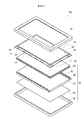
- FIG. 1 is an exploded perspective view schematically showing a configuration of a display device according to an embodiment of the present invention.
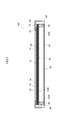
- FIG. 2 is a cross-sectional view schematically showing a configuration of a display device according to an embodiment of the present invention.
- FIG. 3 is a cross-sectional view schematically showing a peripheral portion of the display panel in the display device according to the embodiment of the present invention.
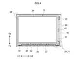
- FIG. 4 is a plan view schematically showing a state in which a protruding member is provided on the exposed portion formed in the peripheral portion of the display panel according to the embodiment of the present invention.
- FIG. 5 is a cross-sectional view schematically showing a peripheral portion of a display panel in a display device according to another embodiment of the present invention.
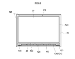
- FIG. 6 is a plan view schematically showing a state in which a protruding member is provided on the exposed portion formed in the peripheral portion of the display panel according to another embodiment of the present invention.
- an active matrix type (TFT type) liquid crystal display device (display device) having a liquid crystal display panel 10 as a display panel for a display device according to a preferred embodiment of the present invention with reference to FIGS. 100 will be described as an example.
- TFT type active matrix type liquid crystal display device
- members and parts having the same action are denoted by the same reference numerals, and redundant description may be omitted or simplified.
- the dimensional relationship (length, width, thickness, etc.) in each drawing does not necessarily accurately reflect the actual dimensional relationship.
- “front” or “front side” means a side facing the viewer (that is, the liquid crystal display panel side) in the liquid crystal display device 100
- “rear side” or “back side” means a liquid crystal display.
- the side of the device 100 that does not face the viewer that is, the backlight unit 80 side) is used.
- the liquid crystal display device 100 includes a liquid crystal display panel 10 and a backlight unit 80 that is an external light source disposed on the back side (lower side in FIG. 1) of the liquid crystal display panel 10. .
- the liquid crystal display panel 10 and the backlight unit 80 are integrally held by being assembled by a bezel (frame body) 70.
- the liquid crystal display panel 10 generally has a rectangular shape having four corners as a whole, and is a region in which a pixel is formed at the center and a display region for displaying an image.
- the liquid crystal display panel 10 is configured by bonding a first substrate 20 and a second substrate 30 facing each other.
- the pair of substrates 20 and 30 are translucent glass substrates and have a sandwich structure composed of a liquid crystal layer 34 sealed therebetween.
- the front side is a color filter substrate (CF substrate) 30 as a second substrate
- the back side is an array substrate (TFT substrate) 20 as a first substrate.
- a sealing material 36 see FIG.
- the sealing material 36 seals the liquid crystal layer 34.
- the liquid crystal layer 34 is composed of a liquid crystal material containing liquid crystal molecules. In such a liquid crystal material, the alignment of liquid crystal molecules is manipulated with the application of an electric field between the substrates 20 and 30, and the optical characteristics change. An alignment film (not shown) that determines the alignment direction of the liquid crystal molecules is formed on the opposite surfaces (inner side) of both the substrates 20 and 30, respectively.
- the polarizing plates 29 and 39 are attached, respectively.
- the array substrate 20 as the first substrate and the CF substrate 30 as the second substrate are different in size from each other, and the array substrate 20 is different from the CF substrate 30. It is formed so as to be relatively large (area).
- an exposed portion 22 is formed in a portion of the peripheral portion of the array substrate 20 that does not overlap the CF substrate 30. That is, at least one peripheral portion of the four sides constituting the rectangular periphery of the array substrate 20 slightly protrudes from the CF substrate 30, and the protruding portion is the exposed portion 22.
- a plurality of flexible printed circuit boards (FPCs) 40 and a plurality of protruding members 50 described later are arranged side by side.
- each of the FPCs 40 an IC chip (driver IC chip) for driving a liquid crystal display panel (not shown) for driving the liquid crystal display panel 10 is mounted.
- one end of the FPC 40 is fixed to the protruding portion 22 so that the FPC 40 is connected to an electrode (typically a pixel electrode or a counter electrode) in the liquid crystal display panel 10.
- the other end of the FPC 40 is attached to a connection board (not shown) which is a printed circuit board (PCB) in which a controller for controlling the driver IC chip and other electronic components are incorporated.
- PCB printed circuit board
- connection board can be disposed on the side surface of the frame 86 by, for example, folding the FPC 40 on the side surface on the outer peripheral side of the frame 86.
- the FPC 40 provided in the liquid crystal display panel 10 includes two of the four sides constituting the rectangular periphery of the array substrate 20. It is fixed to the exposed portion 22 of the side (exposed side 26 described later).
- the backlight unit 80 of the present embodiment is a light source unit that irradiates the liquid crystal display panel 10 with light.
- the backlight unit 80 in the example shown in FIG. 1 is an edge light type backlight unit.
- the backlight unit 80 of the present embodiment includes a light emitting element 82, a light guide plate 84 that irradiates the liquid crystal display panel 10 with light emitted from the light emitting element 82, and a frame (frame body) 86 that houses these. .
- the frame 86 of the present embodiment is made of a metal material (for example, aluminum, iron, etc.) or a resin material having elasticity, and is a box-shaped member that covers the entire back surface of the liquid crystal display device 100.
- a reflection sheet 90 is disposed between the light guide plate 84 and the frame 86 for efficiently reflecting the light from the light emitting element 82 to the front side (viewer side).
- the light guide plate 84 is formed into a rectangular flat plate having a size covering the display area of the liquid crystal display panel 10 by injection molding or the like. As shown in FIG. 2, the light guide plate 84 has a light incident surface 85 ⁇ / b> A on which light from the light emitting element 82 is incident and a light emitting surface 85 ⁇ / b> B that emits the incident light toward the liquid crystal display panel 10.
- the material constituting the light guide plate 84 is not particularly limited as long as it is a material having translucency and excellent moldability. For example, an acrylic resin, a polycarbonate resin, etc. are mentioned.
- a dot pattern (not shown) is formed on the bottom surface of the light guide plate 84 (the surface on the back side and facing the reflection sheet 90) to scatter light and increase the light utilization efficiency.
- Such a dot pattern is formed by printing using an ink or the like that forms a reflection pattern or a diffusion pattern.
- the light emitting element 82 of the present embodiment is a light emitting diode element (LED element).
- LED element light emitting diode element
- the LED element 82 is disposed so as to face the light incident surface 85A of the light guide plate 84, and light emitted from the LED element 82 is incident on the light guide plate 84 from the light incident surface 85A of the light guide plate 84. The light is emitted from the emission surface 85B toward the liquid crystal display panel 10.
- a plurality of sheet-like optical sheets 92 are laminated so as to cover the light guide plate 84.
- the configuration of the optical sheet 92 includes, for example, a diffusion plate, a diffusion sheet, a lens sheet, and a brightness enhancement sheet in order from the frame 86 side, but is not limited to this combination and order.
- the optical sheet 92 is disposed on the front side of the backlight unit 80. Further, as shown in FIGS. 1 and 2, the frame 86 is disposed so as to surround the periphery of the liquid crystal display panel 10 and accommodates the display panel 10. The frame 86 faces the peripheral part of the liquid crystal display panel 10.
- the liquid crystal display panel 10 is disposed on the front side of the optical sheet 92 and is sandwiched between a bezel (frame body) 70 and a frame 86 mounted on the front side of the display panel 10.
- the cushion material 75 that hinders the movement of the display panel 10 in the front-rear direction (that is, the vertical movement in FIG. 3) It is arranged between.
- FIG. 3 is a cross-sectional view schematically showing the periphery of the liquid crystal display panel 10 in the liquid crystal display device 100 according to the present embodiment.
- FIG. 4 is a plan view schematically showing a state in which the protruding member 50 is fixed to the exposed portion 22 formed in the peripheral portion of the liquid crystal display panel 10 according to the present embodiment.
- the protruding member 50 is provided (for example, fixed) on a part of the exposed portion 22 on the array substrate 20.
- a part of the protruding member 50 provided on the array substrate 20 extends beyond the end 24 (that is, the side surface of the array substrate 20) 24 of the array substrate 20 in the direction of the frame 86 (that is, the surface of the array substrate 20). It extends in the direction along the spreading direction (horizontal direction in the drawing). More specifically, as shown in FIG. 4, the protruding member 50 can be disposed on the exposed portion 22 in a region where the FPC 40 is not disposed.
- a part of the protruding member 50 arranged on the exposed portion 22 is a side (exposed side) 26 that does not overlap any of the sides of the CF substrate 30 among the four sides constituting the rectangular periphery of the array substrate 20 In the embodiment, it protrudes in the direction of the frame body (frame) 86 (that is, so as to be parallel to the array substrate 20) beyond the end 24 of the four sides which are the exposed sides 26. Since the exposed side 26 is composed only of the array substrate 20, its strength is weaker than an overlapping side 28 described later. Therefore, when the display panel 10 moves in the frame 86 in the direction of the arrow Y2 or the arrow X2 in FIG. 4 due to vibration or the like, the display panel 10 may be damaged due to contact with the frame 86.
- the end portion 24 of the exposed side 26 is prevented from coming into direct contact with the frame 86. For this reason, damage to the array substrate 20 can be prevented.
- the side (overlapping side) 28 in which the side forming the periphery of the array substrate 20 and the side forming the periphery of the CF substrate 30 overlap has a certain degree of strength. For this reason, the display panel 10 moves in the frame 86 in the direction of the arrow Y1 or the arrow X1 in FIG. The risk of damage to 30 is small.
- a part of the overlapping side 28 is not overlapped with the array substrate 20 and the CF substrate 30 and a part of the array substrate 20 is exposed.
- most of the overlapping side 28 is the array substrate 20.
- the CF substrate 30 overlap each other and have sufficient strength. Therefore, even if the display panel 10 moves in the frame 86 in the direction of the arrow Y1 or the arrow X1 in FIG.
- the protruding member 50 is preferably formed of an elastic material capable of exhibiting a cushioning (cushion) function (that is, capable of absorbing a vibration shock).
- an elastic material polymer materials such as polyethylene terephthalate (PET), polyethylene (PE), polypropylene (PP), polystyrene (PS), polyamide (nylon), and the like are used. What was formed in this is preferable.
- the thickness of the protruding member 50 is not particularly limited, but is preferably a thickness that can exhibit a buffer function.
- a suitable thickness capable of exhibiting a sufficient buffering function is, for example, about 300 ⁇ m to 1000 ⁇ m. For example, as shown in FIG.
- the protruding member 50 is formed in a flat rectangular parallelepiped shape. Further, the protruding member 50 disposed at a corner portion on the exposed portion 22 (that is, a corner portion where the exposed side 26 and the exposed side 26 intersect) among the corner portions of the array substrate 20 is formed in a flat L-shape. And arranged so as to straddle the two exposed sides 26 and 26 of the array substrate 20.
- the shape of the protrusion member 50 is not limited to the above-mentioned shape.
- the exposed portion 22 of the array substrate 20 and the protruding member 50 are fixed (adhered) via a double-sided tape or the like.
- the protruding member 50 made of a synthetic resin (for example, a thermoplastic resin) or other heat-weldable material
- the protruding member 50 is directly attached to the substrate without using a separate adhesive by heating the portion in contact with the substrate. Heat welding (or high frequency welding) may be used.
- the liquid crystal display device 100 including the protruding member 50 as described above accommodates the liquid crystal display panel 10 in the frame 86 and brings the overlapping side 28 of the array substrate 20 into contact with the frame 86.
- the protruding member 50 is exposed to the exposed portion via a double-sided tape or the like so that a part of the protruding member 50 protrudes in the direction of the frame 86 that faces the end portion 24 beyond the end portion 24 of the array substrate 20. It sticks onto 22.
- a bezel (frame body) 70 can be constructed by attaching it to the front surface of the liquid crystal display panel 10.
- the protruding member 50 that can prevent the end portion 24 of the array substrate 20 and the frame 86 from directly contacting each other and prevent the array substrate 20 from being damaged can be disposed.
- the arrangement (fixed) state of can be visually confirmed.
- the protruding member 50 is arranged (adhered) in advance on the exposed portion 22 as described above. Then, the liquid crystal display panel 10 including the protruding member 50 is accommodated in the frame 86. Thereafter, a bezel (frame body) 70 can be constructed by attaching it to the front surface of the liquid crystal display panel 10.
- a part of the protruding member 50 arranged at the corner of the array substrate 20 (that is, the corner where the exposed side 26 and the overlapping side 28 intersect; see FIG. 4). Although it is provided so as to protrude in the direction of the frame 86 beyond the end 24 of the exposed side 26 of the array substrate 20, it overlaps with the overlapping side 28 of the array substrate 20 at the same time as it exceeds the end 24 of the exposed side 26. You may provide so that it may protrude in the direction of the frame 86 beyond the edge part.
- a part of the protruding member 50 protrudes in the direction of the frame 86 beyond the end 24 of the exposed side 26 of the array substrate 20.
- the protruding member 50 according to the present embodiment may be in contact with the frame 86.
- the protruding member 50 is provided on the exposed portion 22 (fixed) so that a part of the protruding member 50 (that is, a portion protruding in the direction of the frame body 86 beyond the end portion 24 of the array substrate 20) is in contact with the frame body 86. ),
- the gap between the liquid crystal display panel 10 and the frame 86 is eliminated. Therefore, it is possible to prevent the array substrate 20 and the frame body 86 from coming into direct contact and to suppress the liquid crystal display panel 10 from moving in the frame body 86, thereby effectively preventing the array substrate 20 from being damaged. can do.
- the present invention is not limited to such a form.
- the present invention is not limited to such a form.
- the present invention is not limited to such a form.
- the protruding members 150 are respectively provided (fixed) at the corners of the exposed portions 122, and a part of the protruding members 150 is the array substrate 120.
- the frame that houses the backlight (ie, LED, light guide plate, etc.) and the array substrate (first substrate) are prevented. It is also possible to prevent contact with a frame (for example, a bezel or the like) different from the frame that accommodates.
- the first substrate constituting the display panel for example, the array substrate
- the frame facing the peripheral portion of the display panel are prevented from coming into direct contact, and the first substrate is prevented from being damaged.
- a liquid crystal display device provided with a protruding member is provided.
- Liquid crystal display panel (display panel) 20 First substrate (array substrate, TFT substrate) 22 Exposed portion 24 End portion 26 Exposed side 28 Overlapping side 29 Polarizing plate 30 Second substrate (color filter substrate, CF substrate) 34 Liquid crystal layer 36 Sealing material 39 Polarizing plate 40 Flexible printed circuit board (FPC) 50 Projecting member 70 Bezel (frame) 75 Cushion material 80 Backlight unit 82 Light emitting element (LED element) 84 Light guide plate 85A Light incident surface 85B Light exit surface 86 Frame (frame) 88 Wiring board 90 Reflective sheet 92 Optical sheet 100 Liquid crystal display device (display device) 110 Liquid crystal display panel (display panel) 120 Array substrate (first substrate) 122 Exposed portion 124 End portion 126 Exposed side 128 Overlapping side 130 CF substrate (second substrate) 150 Protruding member
Landscapes
- Physics & Mathematics (AREA)
- Nonlinear Science (AREA)
- Mathematical Physics (AREA)
- Chemical & Material Sciences (AREA)
- Crystallography & Structural Chemistry (AREA)
- General Physics & Mathematics (AREA)
- Optics & Photonics (AREA)
- Liquid Crystal (AREA)
- Devices For Indicating Variable Information By Combining Individual Elements (AREA)
Abstract
表示装置100は、互いに対向する第1基板20と第2基板30とが貼り合わされてなる表示パネル10と、上記表示パネルの周辺部に対向する枠体86とを備えている。上記第1基板と上記第2基板とは相互に大きさが異なっており、相対的に大きい上記第1基板の周辺部のうち上記第2基板と重なっていない部分には露出部22が形成されている。上記露出部の一部には上記第1基板の端部24を越えて上記枠体の方向に突出する突出部材50が設けられている。
Description
本発明は、表示パネルを備える表示装置に関し、詳しくは、表示パネルの破損を防止する技術に関する。
なお、本出願は2011年4月18日に出願された日本国特許出願2011-092152号に基づく優先権を主張しており、その出願の全内容は本明細書中に参照として組み入れられている。
なお、本出願は2011年4月18日に出願された日本国特許出願2011-092152号に基づく優先権を主張しており、その出願の全内容は本明細書中に参照として組み入れられている。
テレビ、パソコン等の画像表示装置(ディスプレイ)として、典型的には矩形状である液晶表示パネルを備えた液晶表示装置が広く用いられている。
この種の表示装置では、典型的には、上記表示パネルの前面側に枠形状のベゼル(枠体)が配置され、また該パネルの後面側には枠状のフレーム(枠体)が配置されている。これら枠体であるベゼル及びフレームは、それぞれ上記表示パネルの中央における表示領域(アクティブエリア)を矩形状に囲む額縁形状に形成されており、該表示パネルの前後両側から該パネルを挟持している。
かかる表示パネルは、一対の基板(典型的にはアレイ基板及び該アレイ基板に対向するように配置されるカラーフィルタ基板)間に、液晶材料が封じ込められて液晶層として保持されるように構成されている。上記アレイ基板の周辺部のうちカラーフィルタ(CF)基板と重なっていない部分には、表示パネルを駆動するための電子部品等が実装されている。
上記表示パネルをフレーム(枠体)に収容したときに、表示パネルの端部(即ち表示パネルの側面)と該端部に対向する枠体との間に間隙(クリアランス)があると、振動や衝撃等によって表示パネルが移動してフレームに接触する虞がある。上記アレイ基板の周辺部のうちCF基板と重なっていない部分は、重なっている部分と比べて強度が低いため、枠体との接触により破損する虞がある。例えば特許文献1には、ベゼル(枠体)の裏面(表示装置と対向する面)に緩衝部材を配置することにより表示パネルと該表示パネルを収容する枠体との接触を防止しようとする技術が記載されている。
この種の表示装置では、典型的には、上記表示パネルの前面側に枠形状のベゼル(枠体)が配置され、また該パネルの後面側には枠状のフレーム(枠体)が配置されている。これら枠体であるベゼル及びフレームは、それぞれ上記表示パネルの中央における表示領域(アクティブエリア)を矩形状に囲む額縁形状に形成されており、該表示パネルの前後両側から該パネルを挟持している。
かかる表示パネルは、一対の基板(典型的にはアレイ基板及び該アレイ基板に対向するように配置されるカラーフィルタ基板)間に、液晶材料が封じ込められて液晶層として保持されるように構成されている。上記アレイ基板の周辺部のうちカラーフィルタ(CF)基板と重なっていない部分には、表示パネルを駆動するための電子部品等が実装されている。
上記表示パネルをフレーム(枠体)に収容したときに、表示パネルの端部(即ち表示パネルの側面)と該端部に対向する枠体との間に間隙(クリアランス)があると、振動や衝撃等によって表示パネルが移動してフレームに接触する虞がある。上記アレイ基板の周辺部のうちCF基板と重なっていない部分は、重なっている部分と比べて強度が低いため、枠体との接触により破損する虞がある。例えば特許文献1には、ベゼル(枠体)の裏面(表示装置と対向する面)に緩衝部材を配置することにより表示パネルと該表示パネルを収容する枠体との接触を防止しようとする技術が記載されている。
ところで、上記特許文献1に記載されるようにベゼル(枠体)の裏面に緩衝部材を配置したものを用いて表示装置を構築する場合、緩衝部材の寸法誤差や取り付け誤差等によって、緩衝部材がCF基板上に乗り上げてしまう(即ち緩衝部材とCF基板とが重なり合う)虞がある。このとき、かかる緩衝部材は表示パネル(即ちアレイ基板)が枠体に接触することを防止するという機能を果たさなくなる虞がある。さらに、上記構成の表示パネルでは、表示パネルを一旦組立てると緩衝部材がCF基板上に乗り上げているか否かの確認をすることができない。また、緩衝部材とCF基板との間の間隙を広めに設けることによって緩衝部材がCF基板上に乗り上げないようにすると、枠体(典型的にはベゼルの額縁部分)の狭小化の実現が困難となり好ましくない。
そこで、本発明は、かかる点に鑑みてなされたものであり、その目的は、表示パネルの周辺部に対向する枠体と該表示パネルを構成する基板の端部との接触を防止して該基板の破損を防止すると共に、該防止機能を容易に構築可能な表示装置を提供することである。
そこで、本発明は、かかる点に鑑みてなされたものであり、その目的は、表示パネルの周辺部に対向する枠体と該表示パネルを構成する基板の端部との接触を防止して該基板の破損を防止すると共に、該防止機能を容易に構築可能な表示装置を提供することである。
上記目的を実現するべく、本発明により、互いに対向する第1基板と第2基板とが貼り合わされてなる表示パネルと、上記表示パネルの周辺部に対向する枠体と、を備える表示装置が提供される。即ちここで開示される表示装置において、上記第1基板と上記第2基板とは相互に大きさが異なっており、相対的に大きい上記第1基板の周辺部のうち前記第2基板と重なっていない部分には露出部が形成されている。上記露出部、の一部には上記第1基板の端部を越えて上記枠体の方向(即ち第1基板表面の拡がり方向に沿う方向)に突出する突出部材が設けられていることを特徴とする。
本発明に係る表示装置では、第1基板に形成された露出部上に突出部材が設けられており、突出部材は第1基板の端部を越えて枠体の方向に突出している。かかる構成によると、表示装置に振動等が加わり、枠体内に収容された表示パネルが移動するような場合であっても、第1基板の端部から突出する突出部材が枠体と接触し、第1基板の露出部の端部と枠体との直接的な接触を防止することができるため第1基板の破損等を未然に防ぐことができる。
また、上記構成の表示装置では、典型的には、表示パネルを枠体内に収容した後に第1基板の露出部に突出部材を配置(例えば固着)するため、突出部材の取り付け状態を確認することができる。このため、突出部材が他の部分(例えば第2基板)に乗り上げてしまうような不具合もなく表示装置を容易に構築することができる。
ここで開示される表示装置の好適な一形態として液晶表示装置が挙げられる。その形態の表示装置(液晶表示装置)において、好ましくは、上記第1基板はアレイ基板(TFT基板)であり、上記第2基板はカラーフィルタ基板(CF基板)であり、該一対の基板間に液晶層が形成されている。
また、上記構成の表示装置では、典型的には、表示パネルを枠体内に収容した後に第1基板の露出部に突出部材を配置(例えば固着)するため、突出部材の取り付け状態を確認することができる。このため、突出部材が他の部分(例えば第2基板)に乗り上げてしまうような不具合もなく表示装置を容易に構築することができる。
ここで開示される表示装置の好適な一形態として液晶表示装置が挙げられる。その形態の表示装置(液晶表示装置)において、好ましくは、上記第1基板はアレイ基板(TFT基板)であり、上記第2基板はカラーフィルタ基板(CF基板)であり、該一対の基板間に液晶層が形成されている。
ここで開示される表示装置の好適な一態様では、上記突出部材は、上記枠体と接触していることを特徴とする。
かかる構成によると、第1基板の端部が枠体に直接接触するのを防止すると共に、枠体内に収容された表示パネルの動きを抑制することができる。
かかる構成によると、第1基板の端部が枠体に直接接触するのを防止すると共に、枠体内に収容された表示パネルの動きを抑制することができる。
ここで開示される表示装置の好適な他の一態様では、上記突出部材は、弾性を有する材料から形成されていることを特徴とする。
かかる構成によると、表示装置に振動等に伴う衝撃が加わって枠体内に収容された表示パネルが移動するような場合であっても、突出部材によって第1基板と枠体とが直接接触するのを防止すると共に、突出部材が衝撃を吸収し得るため衝撃が突出部材を介して第1基板に伝わることをより効果的に防止することができる。
かかる構成によると、表示装置に振動等に伴う衝撃が加わって枠体内に収容された表示パネルが移動するような場合であっても、突出部材によって第1基板と枠体とが直接接触するのを防止すると共に、突出部材が衝撃を吸収し得るため衝撃が突出部材を介して第1基板に伝わることをより効果的に防止することができる。
ここで開示される表示装置の好適な他の一態様では、上記第1基板は4つの角部を有する矩形状をしており、上記突出部材は、該角部のうち上記露出部の角部に設けられていることを特徴とする。
かかる構成によると、第1基板の端部が枠体に接触することをより効果的に防止することができる。
かかる構成によると、第1基板の端部が枠体に接触することをより効果的に防止することができる。
図面を参照しながら、本発明の好適ないくつかの実施形態を説明する。なお、本明細書において特に言及している事項以外の事柄であって本発明の実施に必要な事柄(例えば、表示パネルの構成や構築方法、表示装置に装備される光源の構成等)は、当該分野における従来技術に基づく当業者の設計事項として把握され得る。本発明は、本明細書に開示されている内容と当該分野における技術常識とに基づいて実施することができる。
以下、図1~図4を参照しながら、本発明の好ましい一実施形態に係る表示装置について、表示パネルとして液晶表示パネル10を備えたアクティブマトリックス方式(TFT型)の液晶表示装置(表示装置)100を例に挙げて説明する。なお、以下の図面において、同じ作用を奏する部材、部位には同じ符号を付し、重複する説明は省略または簡略化することがある。また、各図における寸法関係(長さ、幅、厚さ等)は、必ずしも実際の寸法関係を正確に反映するものではない。また、以下の説明において、「前面」、または「表側」とは液晶表示装置100における視聴者に面する側(すなわち液晶表示パネル側)をいい、「後面」、または「裏側」とは液晶表示装置100における視聴者に面しない側(すなわちバックライトユニット80側)をいうこととする。
図1に示すように、液晶表示装置100は、液晶表示パネル10と、該液晶表示パネル10の裏側(図1における下側)に配置された外部光源であるバックライトユニット80とを備えている。液晶表示パネル10とバックライトユニット80とは、ベゼル(枠体)70により組み付けられることで一体的に保持されている。
図1に示すように、液晶表示パネル10は、概して、全体として4つの角部を有する矩形状をしており、その中央に画素が形成されている領域であって画像を表示する表示領域を有している。図1及び図2に示すように、この液晶表示パネル10は、互いに対向する第1基板20と第2基板30とが貼り合わされて構成されている。上記一対の基板20,30は透光性のガラス基板であって、その間に封入される液晶層34とから構成されるサンドイッチ構造を有している。上記一対の基板20,30のうち、表側が第2基板であるカラーフィルタ基板(CF基板)30であり、裏側が第1基板であるアレイ基板(TFT基板)20である。なお、かかる基板20,30の周辺部には、上記表示領域の周囲を囲むようにシール材36(図3参照)が設けられている。該シール材36は液晶層34を封止している。液晶層34は、液晶分子を含む液晶材料から構成される。かかる液晶材料は、基板20,30の間の電界印加に伴って液晶分子の配向が操作され光学特性が変化する。両基板20,30における互いに対向する側(内側)の面には、それぞれ液晶分子の配向方向を決定する配向膜(図示せず)が形成されており、対向しない側(外側)の面には、それぞれ偏光板29,39が貼り付けられている。
図1及び図4に示すように、上記第1基板であるアレイ基板20と第2基板であるCF基板30とは相互に大きさが異なっており、アレイ基板20は、CF基板30に対して相対的に(面積が)大きくなるように形成されている。該2枚の基板20,30を重ね合わせた際に、アレイ基板20の周辺部のうちCF基板30と重なっていない部分には露出部22が形成されている。即ち、アレイ基板20の矩形状の周辺を構成する四辺のうち少なくとも一辺の周辺部がCF基板30からわずかにはみ出しており、該はみ出した部分が露出部22である。
かかる露出部22には、複数のフレキシブルプリント基板(FPC)40と後述する複数の突出部材50とが並んで配置されている。FPC40のそれぞれには、液晶表示パネル10を駆動するための図示しない液晶表示パネル駆動用のICチップ(ドライバICチップ)が搭載されている。このような構成のFPC40において、その一方の端部は上記はみ出た露出部22に固定されることにより、該FPC40が液晶表示パネル10内の電極(典型的には画素電極や対向電極等)に接続される。また、該FPC40の他方の端部は、上記ドライバICチップを制御するコントローラやその他の電子部品などが組み込まれたプリント回路基板(PCB)である接続基板(図示せず)に取り付けられている。接続基板は、例えば、FPC40がフレーム86の外周側の側面に折り込まれることにより、フレーム86の側面に配設され得る。
図1及び図4に示すように、本実施形態に係る液晶表示パネル10において、該液晶表示パネル10に設けられたFPC40は、上記アレイ基板20の矩形状の周辺を構成する四辺のうちの二辺(後述する露出辺26)の露出部22に固定されている。
かかる露出部22には、複数のフレキシブルプリント基板(FPC)40と後述する複数の突出部材50とが並んで配置されている。FPC40のそれぞれには、液晶表示パネル10を駆動するための図示しない液晶表示パネル駆動用のICチップ(ドライバICチップ)が搭載されている。このような構成のFPC40において、その一方の端部は上記はみ出た露出部22に固定されることにより、該FPC40が液晶表示パネル10内の電極(典型的には画素電極や対向電極等)に接続される。また、該FPC40の他方の端部は、上記ドライバICチップを制御するコントローラやその他の電子部品などが組み込まれたプリント回路基板(PCB)である接続基板(図示せず)に取り付けられている。接続基板は、例えば、FPC40がフレーム86の外周側の側面に折り込まれることにより、フレーム86の側面に配設され得る。
図1及び図4に示すように、本実施形態に係る液晶表示パネル10において、該液晶表示パネル10に設けられたFPC40は、上記アレイ基板20の矩形状の周辺を構成する四辺のうちの二辺(後述する露出辺26)の露出部22に固定されている。
本実施形態のバックライトユニット80は、液晶表示パネル10に光を照射する光源ユニットである。図1に示した例のバックライトユニット80は、エッジライト型のバックライトユニットである。本実施形態のバックライトユニット80は、発光素子82と、発光素子82が発した光を液晶表示パネル10に照射させる導光板84と、これらを収納するフレーム(枠体)86とを備えている。本実施形態のフレーム86は、金属材料(例えば、アルミニウム、鉄など)や弾性を有する樹脂材料から構成されており、液晶表示装置100の裏面全体を覆う箱型形状の部材である。導光板84とフレーム86との間には、発光素子82の光を効率的に表側(観視者側)に反射させるための反射シート90が配置されている。
導光板84は、液晶表示パネル10の表示領域を覆う大きさの長方形の平板状に射出成形等によって形成されている。図2に示すように、導光板84は、発光素子82からの光が入射する光入射面85A及び該入射した光を液晶表示パネル10に向けて出射する光出射面85Bを有している。導光板84を構成する材料は、透光性を有し成形性に優れる材料であれば特に制限されない。例えば、アクリル樹脂、ポリカーボネート樹脂等が挙げられる。導光板84の底面(裏側の面であって反射シート90に対向する面)には、光を散乱させて光の利用効率を高めるドットパターン(図示せず)が形成されている。かかるドットパターンは、反射パターン又は拡散パターンを形成するインクなどを用いて印刷によって形成されている。
本実施形態の発光素子82は、発光ダイオード素子(LED素子)である。図1に示した構成例では、発光素子としての複数のLED素子82が配線基板88の上に載置されている。LED素子82は、導光板84の光入射面85Aに対向して配置されており、LED素子82から出射された光は、導光板84の光入射面85Aから導光板84内に入射され、光出射面85Bから液晶表示パネル10に向けて出射される。
本実施形態の発光素子82は、発光ダイオード素子(LED素子)である。図1に示した構成例では、発光素子としての複数のLED素子82が配線基板88の上に載置されている。LED素子82は、導光板84の光入射面85Aに対向して配置されており、LED素子82から出射された光は、導光板84の光入射面85Aから導光板84内に入射され、光出射面85Bから液晶表示パネル10に向けて出射される。
また、導光板86の表側(即ち導光板86と液晶表示パネル10との間)には、複数のシート状の光学シート92が積層されて該導光板84を覆うように配置されている。光学シート92の構成としては、例えば、フレーム86側から順に、拡散板、拡散シート、レンズシート、および輝度上昇シートから構成されているが、この組合せおよび順序に限定されない。
上述のように、バックライトユニット80の前面側には光学シート92が配置されている。さらに、図1及び2に示すように、フレーム86は、液晶表示パネル10の周辺部を囲むように配置されて該表示パネル10を収容している。フレーム86は、液晶表示パネル10の周辺部に対向している。液晶表示パネル10は、光学シート92の前面側に配置されており、該表示パネル10の前面側に装着されたベゼル(枠体)70とフレーム86とに挟持されている。なお、図3に示すように、本実施形態に係る液晶表示装置100では、表示パネル10の前後方向の動き(即ち図3の上下方向の動き)を妨げるクッション材75が表示パネル10とベゼル70との間に配置されている。
次に、図3及び図4を参照しつつ本実施形態(第1実施形態)に係る液晶表示装置100に具備される突出部材50の構成およびその配置(固着)について詳細に説明する。図3は、本実施形態に係る液晶表示装置100における液晶表示パネル10の周辺部を模式手に示す断面図である。図4は、本実施形態に係る液晶表示パネル10の周辺部に形成された露出部22に突出部材50が固着された状態を模式的に示す平面図である。
図3及び図4に示すように、本実施形態に係る突出部材50は、アレイ基板20上の露出部22の一部に設けられている(例えば固着されている)。アレイ基板20上に設けられた突出部材50は、その一部がアレイ基板20の端部(即ちアレイ基板20の側面)24を越えて枠体(フレーム)86の方向(即ちアレイ基板20の表面の拡がり方向に沿う方向:図面における水平方向)に突出している。より具体的には、突出部材50は、図4に示すように、露出部22上であってFPC40が配置されていない領域に配置され得る。露出部22上に配置された突出部材50の一部は、アレイ基板20の矩形状の周辺を構成する四辺のうちCF基板30のいずれかの辺とも重なっていない辺(露出辺)26(本実施形態では四辺のうち二辺が露出辺26である)の端部24を越えて枠体(フレーム)86の方向に(即ちアレイ基板20と平行となるように)突出している。
露出辺26はアレイ基板20のみからなるため後述する重複辺28と比べると強度が弱い。このため、振動等によって表示パネル10が枠体86内を図4の矢印Y2又は矢印X2の方向に移動すると、枠体86との接触によって破損してしまう虞がある。しかし、本実施形態のように露出部22上に突出部材50を配置することで露出辺26の端部24が枠体86に直接接触することが防止される。このため、アレイ基板20の破損を防止することができる。一方、アレイ基板20の周辺を構成する辺とCF基板30の周辺を構成する辺とが重なっている辺(重複辺)28は、強度がある程度高い。このため、表示パネル10が枠体86内を図4の矢印Y1又は矢印X1の方向に移動することによって、重複辺28が枠体86と直接接触する場合であってもアレイ基板20及びCF基板30の破損の虞は小さい。なお、本実施形態の重複辺28の一部は、アレイ基板20とCF基板30とが重なっておらずアレイ基板20の一部が露出しているが、重複辺28の大部分はアレイ基板20とCF基板30とが重なっており十分な強度を備えている。このため、表示パネル10が枠体86内を図4の矢印Y1又は矢印X1の方向に移動してもアレイ基板20の破損の虞は小さい。
露出辺26はアレイ基板20のみからなるため後述する重複辺28と比べると強度が弱い。このため、振動等によって表示パネル10が枠体86内を図4の矢印Y2又は矢印X2の方向に移動すると、枠体86との接触によって破損してしまう虞がある。しかし、本実施形態のように露出部22上に突出部材50を配置することで露出辺26の端部24が枠体86に直接接触することが防止される。このため、アレイ基板20の破損を防止することができる。一方、アレイ基板20の周辺を構成する辺とCF基板30の周辺を構成する辺とが重なっている辺(重複辺)28は、強度がある程度高い。このため、表示パネル10が枠体86内を図4の矢印Y1又は矢印X1の方向に移動することによって、重複辺28が枠体86と直接接触する場合であってもアレイ基板20及びCF基板30の破損の虞は小さい。なお、本実施形態の重複辺28の一部は、アレイ基板20とCF基板30とが重なっておらずアレイ基板20の一部が露出しているが、重複辺28の大部分はアレイ基板20とCF基板30とが重なっており十分な強度を備えている。このため、表示パネル10が枠体86内を図4の矢印Y1又は矢印X1の方向に移動してもアレイ基板20の破損の虞は小さい。
突出部材50は、緩衝(クッション)機能を発揮し得る(すなわち振動衝撃を吸収し得る)弾性を有する材料から形成されていることが好ましい。このような弾性材料の一好適例としては、ポリエチレンテレフタレート(PET),ポリエチレン(PE),ポリプロピレン(PP),ポリスチレン(PS),ポリアミド(ナイロン)等のポリマー材料が挙げられ、かかる材料からシート状に形成されたものが好ましい。突出部材50の厚さは、特に制限はないが緩衝機能を発揮し得る厚さであることが好ましい。十分な緩衝機能を発揮し得る好適な厚さとしては、例えば凡そ300μm~1000μm程度が適当である。
突出部材50は、例えば、図4に示すように、扁平な直方体形状に形成されている。また、アレイ基板20の角部のうち露出部22上にある角部(即ち露出辺26と露出辺26とが交わる角部)に配置される突出部材50は、扁平なL字形状に形成されており、アレイ基板20の二つの露出辺26,26上に跨るように配置されている。なお、突出部材50の形状は上述の形状に限定されない。
上記アレイ基板20の露出部22に設けられている突出部材50を露出部22に固着する場合、その方法としては、突出部材50が露出部22から外れない限り特に制限はない。例えば、両面テープ等を介してアレイ基板20の露出部22と突出部材50とを固着(接着)することが挙げられる。或いは、合成樹脂(例えば熱可塑性樹脂)その他の熱溶着可能な素材からなる突出部材50である場合は、基板に接触する部分を加熱して別途接着剤を使用することなく突出部材50を直接基板に熱溶着(若しくは高周波溶着)してもよい。
突出部材50は、例えば、図4に示すように、扁平な直方体形状に形成されている。また、アレイ基板20の角部のうち露出部22上にある角部(即ち露出辺26と露出辺26とが交わる角部)に配置される突出部材50は、扁平なL字形状に形成されており、アレイ基板20の二つの露出辺26,26上に跨るように配置されている。なお、突出部材50の形状は上述の形状に限定されない。
上記アレイ基板20の露出部22に設けられている突出部材50を露出部22に固着する場合、その方法としては、突出部材50が露出部22から外れない限り特に制限はない。例えば、両面テープ等を介してアレイ基板20の露出部22と突出部材50とを固着(接着)することが挙げられる。或いは、合成樹脂(例えば熱可塑性樹脂)その他の熱溶着可能な素材からなる突出部材50である場合は、基板に接触する部分を加熱して別途接着剤を使用することなく突出部材50を直接基板に熱溶着(若しくは高周波溶着)してもよい。
以上のような突出部材50を備える液晶表示装置100は、例えば、液晶表示パネル10を枠体86内に収容してアレイ基板20の重複辺28を枠体86に接触させる。かかる状態で、突出部材50の一部がアレイ基板20の端部24を越えて該端部24に対向する枠体86の方向に突出するように突出部材50を両面テープ等を介して露出部22上に固着する。その後にベゼル(枠体)70を液晶表示パネル10の前面に装着することにより構築することができる。このようにして、アレイ基板20の端部24と枠体86とが直接接触するのを防止してアレイ基板20の破損を防止し得る突出部材50を配置することができ、また、突出部材50の配置(固着)状態を目視で確認することができる。また、別の例として、予め露出部22上に上記のように突出部材50を配置(固着)しておく。そして、突出部材50を備える液晶表示パネル10を枠体86内に収容する。その後にベゼル(枠体)70を液晶表示パネル10の前面に装着することにより構築することができる。なお、本実施形態に係る液晶表示装置100では、アレイ基板20の角部(即ち露出辺26と重複辺28とが交わる角部。図4参照。)に配置された突出部材50の一部は、アレイ基板20の露出辺26の端部24を越えて枠体86の方向に突出するように設けられているが、露出辺26の端部24を越えるのと同時にアレイ基板20の重複辺28の端部を越えて枠体86の方向に突出するように設けてもよい。
上述した第1実施形態に係る液晶表示装置100では、突出部材50の一部は、アレイ基板20の露出辺26の端部24を越えて枠体86の方向に突出しており、枠体86と接触していないが、図5に示すように、本実施形態(第2実施形態)に係る突出部材50は枠体86と接触していてもよい。突出部材50の一部(即ちアレイ基板20の端部24を越えて枠体86の方向に突出した部分)が枠体86と接触するように、突出部材50を露出部22に設ける(固着する)ことによって、液晶表示パネル10と枠体86との間隙がなくなる。このためアレイ基板20と枠体86とが直接接触するのを防止する共に、液晶表示パネル10が枠体86内を移動することを抑制することができ、アレイ基板20の破損を効果的に防止することができる。
また、上述した第1実施形態に係る液晶表示パネル10では、アレイ基板20の矩形状の周辺を構成する四辺のうち二辺が露出辺26であったが、かかる形態に限定されない。例えば、図6に示すように、アレイ基板(第1基板)120の周辺を構成する四辺のうち三辺がCF基板(第2基板)の周辺を構成する辺と重なっている辺(重複辺128)であり、一辺が重なっていない辺(露出辺)126の場合であってもよい。本実施形態(第3実施形態)に係る液晶表示パネル110では、露出部122の角部に突出部材150がそれぞれ設けられており(固着されており)、突出部材150の一部がアレイ基板120の露出辺126の端部124を越えて枠体86の方向に突出するように配置されている。なお、アレイ基板の矩形状の周辺を構成する三辺がCF基板の周辺を構成する辺と重なっていない場合(即ち3辺が露出辺の場合)、或いはアレイ基板の全周がCF基板の周辺を構成する辺と重なっていない場合(即ち4辺全てが露出辺の場合)には、露出部上であって露出辺から、該辺に対向する枠体の方向に突出するように突出部材を配置する。
以上、本発明の具体例を図面を参照しつつ詳細に説明したが、これらは例示にすぎず、特許請求の範囲を限定するものではない。特許請求の範囲に記載の技術には、以上に例示した具体例を様々に変形、変更したものが含まれる。
例えば、上述した種々の実施形態では、バックライト(即ちLED、導光板等)を収容するフレーム(枠体)とアレイ基板(第1基板)との接触を防止するものであったが、バックライトを収容する枠体とは別の枠体(例えばベゼル等)との接触を防止するものであってもよい。
例えば、上述した種々の実施形態では、バックライト(即ちLED、導光板等)を収容するフレーム(枠体)とアレイ基板(第1基板)との接触を防止するものであったが、バックライトを収容する枠体とは別の枠体(例えばベゼル等)との接触を防止するものであってもよい。
本発明によると、表示パネルを構成する第1基板(例えばアレイ基板)と表示パネルの周辺部に対向する枠体とが直接接触することを防止して第1基板に破損が発生することを防ぐ突出部材を具備した液晶表示装置が提供される。
10 液晶表示パネル(表示パネル)
20 第1基板(アレイ基板、TFT基板)
22 露出部
24 端部
26 露出辺
28 重複辺
29 偏光板
30 第2基板(カラーフィルタ基板、CF基板)
34 液晶層
36 シール材
39 偏光板
40 フレキシブルプリント基板(FPC)
50 突出部材
70 ベゼル(枠体)
75 クッション材
80 バックライトユニット
82 発光素子(LED素子)
84 導光板
85A 光入射面
85B 光出射面
86 フレーム(枠体)
88 配線基板
90 反射シート
92 光学シート
100 液晶表示装置(表示装置)
110 液晶表示パネル(表示パネル)
120 アレイ基板(第1基板)
122 露出部
124 端部
126 露出辺
128 重複辺
130 CF基板(第2基板)
150 突出部材
20 第1基板(アレイ基板、TFT基板)
22 露出部
24 端部
26 露出辺
28 重複辺
29 偏光板
30 第2基板(カラーフィルタ基板、CF基板)
34 液晶層
36 シール材
39 偏光板
40 フレキシブルプリント基板(FPC)
50 突出部材
70 ベゼル(枠体)
75 クッション材
80 バックライトユニット
82 発光素子(LED素子)
84 導光板
85A 光入射面
85B 光出射面
86 フレーム(枠体)
88 配線基板
90 反射シート
92 光学シート
100 液晶表示装置(表示装置)
110 液晶表示パネル(表示パネル)
120 アレイ基板(第1基板)
122 露出部
124 端部
126 露出辺
128 重複辺
130 CF基板(第2基板)
150 突出部材
Claims (5)
- 互いに対向する第1基板と第2基板とが貼り合わされてなる表示パネルと、
前記表示パネルの周辺部に対向する枠体と、
を備える表示装置であって、
前記第1基板と前記第2基板とは相互に大きさが異なっており、相対的に大きい前記第1基板の周辺部のうち前記第2基板と重なっていない部分には露出部が形成されており、
前記露出部の一部には、前記第1基板の端部を越えて前記枠体の方向に突出する突出部材が設けられていることを特徴とする、表示装置。 - 前記突出部材は、前記枠体と接触していることを特徴とする、請求項1に記載の表示装置。
- 前記突出部材は、弾性を有する材料から形成されていることを特徴とする、請求項1又は2に記載の表示装置。
- 前記第1基板は4つの角部を有する矩形状をしており、前記突出部材は、該角部のうち前記露出部の角部に設けられていることを特徴とする、請求項1から3のいずれか一項に記載の表示装置。
- 前記第1基板はアレイ基板であり、前記第2基板はカラーフィルタ基板であって、該一対の基板間に液晶層が形成されていることを特徴とする、請求項1から4のいずれか一項に記載の表示装置。
Priority Applications (1)
| Application Number | Priority Date | Filing Date | Title |
|---|---|---|---|
| JP2013510959A JPWO2012144387A1 (ja) | 2011-04-18 | 2012-04-11 | 表示装置 |
Applications Claiming Priority (2)
| Application Number | Priority Date | Filing Date | Title |
|---|---|---|---|
| JP2011-092152 | 2011-04-18 | ||
| JP2011092152 | 2011-04-18 |
Publications (1)
| Publication Number | Publication Date |
|---|---|
| WO2012144387A1 true WO2012144387A1 (ja) | 2012-10-26 |
Family
ID=47041498
Family Applications (1)
| Application Number | Title | Priority Date | Filing Date |
|---|---|---|---|
| PCT/JP2012/059906 Ceased WO2012144387A1 (ja) | 2011-04-18 | 2012-04-11 | 表示装置 |
Country Status (2)
| Country | Link |
|---|---|
| JP (1) | JPWO2012144387A1 (ja) |
| WO (1) | WO2012144387A1 (ja) |
Citations (2)
| Publication number | Priority date | Publication date | Assignee | Title |
|---|---|---|---|---|
| JPH08179288A (ja) * | 1994-12-27 | 1996-07-12 | Sharp Corp | 液晶表示装置 |
| JPH08313880A (ja) * | 1995-05-18 | 1996-11-29 | Rohm Co Ltd | 液晶表示装置およびその製法 |
-
2012
- 2012-04-11 JP JP2013510959A patent/JPWO2012144387A1/ja active Pending
- 2012-04-11 WO PCT/JP2012/059906 patent/WO2012144387A1/ja not_active Ceased
Patent Citations (2)
| Publication number | Priority date | Publication date | Assignee | Title |
|---|---|---|---|---|
| JPH08179288A (ja) * | 1994-12-27 | 1996-07-12 | Sharp Corp | 液晶表示装置 |
| JPH08313880A (ja) * | 1995-05-18 | 1996-11-29 | Rohm Co Ltd | 液晶表示装置およびその製法 |
Also Published As
| Publication number | Publication date |
|---|---|
| JPWO2012144387A1 (ja) | 2014-07-28 |
Similar Documents
| Publication | Publication Date | Title |
|---|---|---|
| US10705277B2 (en) | Display device | |
| JP5933509B2 (ja) | 液晶表示装置 | |
| US20150301266A1 (en) | Lighting device and display device | |
| US20170127166A1 (en) | Lighting device and display device | |
| JP2014142614A (ja) | 液晶表示装置 | |
| US20140192497A1 (en) | Display module and display device including the display module | |
| WO2013002117A1 (ja) | バックライト装置及び該バックライト装置を備える液晶表示装置 | |
| JP2015114643A (ja) | 液晶表示装置 | |
| JP4568209B2 (ja) | バックライト及びそれを用いた液晶表示装置 | |
| JP2013015637A (ja) | 液晶表示装置 | |
| KR102260858B1 (ko) | 액정표시장치 및 액정표시장치의 모듈화방법 | |
| WO2013099765A1 (ja) | 表示装置及び枠部材 | |
| KR102491720B1 (ko) | 액정 표시 장치 | |
| JP2014178551A (ja) | 液晶表示装置 | |
| KR102110296B1 (ko) | 액정표시장치 | |
| JP2014142379A (ja) | 平面表示装置 | |
| KR102271067B1 (ko) | 액정표시장치 | |
| KR102376312B1 (ko) | 액정표시장치 | |
| WO2012173077A1 (ja) | 表示装置、及びテレビ受信装置 | |
| WO2012144387A1 (ja) | 表示装置 | |
| JP2005100692A (ja) | 面状光源装置及びこれを用いた液晶表示装置 | |
| CN111694186A (zh) | 显示装置 | |
| US9891660B2 (en) | Display device | |
| KR20170080791A (ko) | 액정표시장치를 구비한 전자기기 | |
| KR102523535B1 (ko) | 표시장치 |
Legal Events
| Date | Code | Title | Description |
|---|---|---|---|
| 121 | Ep: the epo has been informed by wipo that ep was designated in this application |
Ref document number: 12774408 Country of ref document: EP Kind code of ref document: A1 |
|
| ENP | Entry into the national phase |
Ref document number: 2013510959 Country of ref document: JP Kind code of ref document: A |
|
| NENP | Non-entry into the national phase |
Ref country code: DE |
|
| 122 | Ep: pct application non-entry in european phase |
Ref document number: 12774408 Country of ref document: EP Kind code of ref document: A1 |