WO2012144228A1 - Circuit module - Google Patents
Circuit module Download PDFInfo
- Publication number
- WO2012144228A1 WO2012144228A1 PCT/JP2012/002741 JP2012002741W WO2012144228A1 WO 2012144228 A1 WO2012144228 A1 WO 2012144228A1 JP 2012002741 W JP2012002741 W JP 2012002741W WO 2012144228 A1 WO2012144228 A1 WO 2012144228A1
- Authority
- WO
- WIPO (PCT)
- Prior art keywords
- electrode
- transmission
- reception
- ground electrode
- ground
- Prior art date
Links
Images


Classifications
-
- H—ELECTRICITY
- H03—ELECTRONIC CIRCUITRY
- H03H—IMPEDANCE NETWORKS, e.g. RESONANT CIRCUITS; RESONATORS
- H03H9/00—Networks comprising electromechanical or electro-acoustic devices; Electromechanical resonators
- H03H9/02—Details
- H03H9/05—Holders; Supports
- H03H9/0538—Constructional combinations of supports or holders with electromechanical or other electronic elements
- H03H9/0566—Constructional combinations of supports or holders with electromechanical or other electronic elements for duplexers
-
- H—ELECTRICITY
- H01—ELECTRIC ELEMENTS
- H01P—WAVEGUIDES; RESONATORS, LINES, OR OTHER DEVICES OF THE WAVEGUIDE TYPE
- H01P5/00—Coupling devices of the waveguide type
- H01P5/12—Coupling devices having more than two ports
-
- H—ELECTRICITY
- H04—ELECTRIC COMMUNICATION TECHNIQUE
- H04M—TELEPHONIC COMMUNICATION
- H04M1/00—Substation equipment, e.g. for use by subscribers
- H04M1/02—Constructional features of telephone sets
- H04M1/0202—Portable telephone sets, e.g. cordless phones, mobile phones or bar type handsets
-
- H—ELECTRICITY
- H05—ELECTRIC TECHNIQUES NOT OTHERWISE PROVIDED FOR
- H05K—PRINTED CIRCUITS; CASINGS OR CONSTRUCTIONAL DETAILS OF ELECTRIC APPARATUS; MANUFACTURE OF ASSEMBLAGES OF ELECTRICAL COMPONENTS
- H05K1/00—Printed circuits
- H05K1/02—Details
- H05K1/0213—Electrical arrangements not otherwise provided for
- H05K1/0216—Reduction of cross-talk, noise or electromagnetic interference
- H05K1/0218—Reduction of cross-talk, noise or electromagnetic interference by printed shielding conductors, ground planes or power plane
- H05K1/0224—Patterned shielding planes, ground planes or power planes
- H05K1/0227—Split or nearly split shielding or ground planes
-
- H—ELECTRICITY
- H05—ELECTRIC TECHNIQUES NOT OTHERWISE PROVIDED FOR
- H05K—PRINTED CIRCUITS; CASINGS OR CONSTRUCTIONAL DETAILS OF ELECTRIC APPARATUS; MANUFACTURE OF ASSEMBLAGES OF ELECTRICAL COMPONENTS
- H05K1/00—Printed circuits
- H05K1/02—Details
- H05K1/0213—Electrical arrangements not otherwise provided for
- H05K1/0216—Reduction of cross-talk, noise or electromagnetic interference
- H05K1/023—Reduction of cross-talk, noise or electromagnetic interference using auxiliary mounted passive components or auxiliary substances
- H05K1/0233—Filters, inductors or a magnetic substance
-
- H—ELECTRICITY
- H05—ELECTRIC TECHNIQUES NOT OTHERWISE PROVIDED FOR
- H05K—PRINTED CIRCUITS; CASINGS OR CONSTRUCTIONAL DETAILS OF ELECTRIC APPARATUS; MANUFACTURE OF ASSEMBLAGES OF ELECTRICAL COMPONENTS
- H05K1/00—Printed circuits
- H05K1/02—Details
- H05K1/0213—Electrical arrangements not otherwise provided for
- H05K1/0237—High frequency adaptations
- H05K1/0243—Printed circuits associated with mounted high frequency components
-
- H—ELECTRICITY
- H05—ELECTRIC TECHNIQUES NOT OTHERWISE PROVIDED FOR
- H05K—PRINTED CIRCUITS; CASINGS OR CONSTRUCTIONAL DETAILS OF ELECTRIC APPARATUS; MANUFACTURE OF ASSEMBLAGES OF ELECTRICAL COMPONENTS
- H05K1/00—Printed circuits
- H05K1/02—Details
- H05K1/11—Printed elements for providing electric connections to or between printed circuits
- H05K1/111—Pads for surface mounting, e.g. lay-out
- H05K1/112—Pads for surface mounting, e.g. lay-out directly combined with via connections
- H05K1/113—Via provided in pad; Pad over filled via
-
- H—ELECTRICITY
- H05—ELECTRIC TECHNIQUES NOT OTHERWISE PROVIDED FOR
- H05K—PRINTED CIRCUITS; CASINGS OR CONSTRUCTIONAL DETAILS OF ELECTRIC APPARATUS; MANUFACTURE OF ASSEMBLAGES OF ELECTRICAL COMPONENTS
- H05K2201/00—Indexing scheme relating to printed circuits covered by H05K1/00
- H05K2201/09—Shape and layout
- H05K2201/09209—Shape and layout details of conductors
- H05K2201/095—Conductive through-holes or vias
- H05K2201/09618—Via fence, i.e. one-dimensional array of vias
-
- H—ELECTRICITY
- H05—ELECTRIC TECHNIQUES NOT OTHERWISE PROVIDED FOR
- H05K—PRINTED CIRCUITS; CASINGS OR CONSTRUCTIONAL DETAILS OF ELECTRIC APPARATUS; MANUFACTURE OF ASSEMBLAGES OF ELECTRICAL COMPONENTS
- H05K2201/00—Indexing scheme relating to printed circuits covered by H05K1/00
- H05K2201/10—Details of components or other objects attached to or integrated in a printed circuit board
- H05K2201/10007—Types of components
- H05K2201/1006—Non-printed filter
Landscapes
- Physics & Mathematics (AREA)
- Engineering & Computer Science (AREA)
- Electromagnetism (AREA)
- Microelectronics & Electronic Packaging (AREA)
- Acoustics & Sound (AREA)
- Signal Processing (AREA)
- Transceivers (AREA)
- Surface Acoustic Wave Elements And Circuit Networks Thereof (AREA)
Abstract
Provided is a technique for improving the characteristic of isolation between transmitting and receiving electrodes provided on an implementation board on which a branching filter is mounted. Even if a transmitted signal, which is outputted from a transmitting electrode (21) of an implementation board (2) to a transmitting terminal of a branching filter (10), leaks to a ground electrode (24), the transmitted signal thus having leaked to the ground electrode (24) then flows into the via conductors (25) that are connected along edges of the ground electrode (24), which edges are adjacent to the transmitting electrode (21), and that are further connected to the ground lines of the motherboard, so that the transmitted signal outputted from the transmitting electrode (21) and leaking into the ground electrode (24) can be prevented from propagating along the edges of the ground electrode (24) to the side of receiving electrodes (22), thereby improving the characteristic of isolation between the transmitting and receiving electrodes (21, 22) provided on the implementation board (2) on which the branching filter (10) is mounted.
Description
本発明は、通過帯域が異なる送信フィルタおよび受信フィルタを有する分波器を備える回路モジュールに関する。
The present invention relates to a circuit module including a duplexer having a transmission filter and a reception filter having different pass bands.
近年、GSM(Global System for Mobile Communications)規格やCDMA(Code Division Multiple Access)規格などの複数の通信規格による通信をサポートする携帯電話や携帯情報端末などの通信携帯端末が急速に普及しており、これらの通信携帯端末では、共通のアンテナを用いて異なる周波数帯域の信号の送受信が行われる。したがって、周波数の異なる送信信号および受信信号を分波する分波器(デュプレクサ)を備えるアンテナスイッチなどのフロントエンドモジュール(回路モジュール)の更なる高性能化および小型化の要求が高まっている。
In recent years, mobile communication terminals such as mobile phones and personal digital assistants that support communication based on multiple communication standards such as the GSM (Global System for Mobile Communications) standard and the CDMA (Code Division Multiple Access) standard are rapidly spreading. In these communication portable terminals, signals in different frequency bands are transmitted and received using a common antenna. Therefore, there is an increasing demand for higher performance and miniaturization of a front end module (circuit module) such as an antenna switch including a duplexer that demultiplexes transmission signals and reception signals having different frequencies.
例えば、図7に示すように、信号の通過帯域が異なる第1および第2のフィルタ部503,505が、各フィルタ部503,505の特性が劣化しないように近接配置されることにより小型化および高性能化が図られた分波器500が、回路モジュールが備える実装用基板に搭載されることで、回路モジュールの小型化および高性能化が図られている。図7に示す従来の分波器500は、プリント基板、LTCC基板、アルミナ系基板、ガラス基板、複合材料基板など、樹脂やセラミック、ポリマー材料から成るベース基板501の実装面に、SAW(表面弾性派)フィルタ素子502を含む第1のフィルタ部503と、SAWフィルタ素子504を含む第2のフィルタ部505とを有し、第1および第2のフィルタ部503,505には、それぞれ、SAWフィルタ素子502,504の電気的特性を補完する周辺回路素子として、チップインダクタ506およびチップコンデンサ507などの受動素子が設けられている。
For example, as shown in FIG. 7, the first and second filter units 503 and 505 having different signal pass bands are arranged close to each other so that the characteristics of the filter units 503 and 505 are not deteriorated. The duplexer 500 with improved performance is mounted on a mounting substrate included in the circuit module, thereby reducing the size and performance of the circuit module. A conventional duplexer 500 shown in FIG. 7 has a SAW (surface elasticity) on a mounting surface of a base substrate 501 made of resin, ceramic, or polymer material such as a printed circuit board, LTCC substrate, alumina substrate, glass substrate, or composite material substrate. A first filter unit 503 including a filter element 502 and a second filter unit 505 including a SAW filter element 504. The first and second filter units 503 and 505 include SAW filters, respectively. As peripheral circuit elements that complement the electrical characteristics of the elements 502 and 504, passive elements such as a chip inductor 506 and a chip capacitor 507 are provided.
そして、インダクタ素子相互の電磁的な干渉を抑制し、各フィルタ部503,505間での信号の干渉を防止するために、第1のフィルタ部503と第2のフィルタ部505との境界部508に配置されて隣り合うチップインダクタ506は、磁束の向きが互いにほぼ直交するようにベース基板501上に配置されている。このように構成すれば、各フィルタ部503,505が近接配置されても、第1および第2のフィルタ部503,505間での信号の干渉が防止され、各フィルタ部503,505の特性変化が低減される。
In order to suppress electromagnetic interference between the inductor elements and to prevent signal interference between the filter units 503 and 505, a boundary part 508 between the first filter unit 503 and the second filter unit 505 is used. The adjacent chip inductors 506 are arranged on the base substrate 501 so that the directions of the magnetic fluxes are substantially orthogonal to each other. With this configuration, even when the filter units 503 and 505 are arranged close to each other, signal interference between the first and second filter units 503 and 505 is prevented, and the characteristic change of each filter unit 503 and 505 is prevented. Is reduced.
このように小型化および高性能化が図られた従来の分波器500が実装用基板に搭載されて、分波器500の第1および第2のフィルタ部503,505が、それぞれ送信フィルタおよび受信フィルタとして利用されることで、アンテナスイッチなどの回路モジュールが形成される。
Thus, the conventional duplexer 500 with reduced size and higher performance is mounted on the mounting substrate, and the first and second filter sections 503 and 505 of the duplexer 500 are respectively connected to the transmission filter and the transmission filter. By being used as a reception filter, a circuit module such as an antenna switch is formed.
また、分波器500は、実装用基板側から送信信号を送信フィルタに入力するための送信端子と、受信フィルタから実装用基板側に受信信号を出力するための受信端子と、送信フィルタの出力側および受信フィルタの入力側に接続されるアンテナ端子(共通端子)と、接地端子とを有しており、実装用基板には、分波器500の送信端子および受信端子にそれぞれ接続される送信電極および受信電極が設けられている。そして、実装用基板の送信電極から分波器500が備える送信フィルタに送信端子を介して送信信号が出力され、送信フィルタに入力された送信信号は、所定のフィルタ処理が施されて分波器500のアンテナ端子から出力される。また、アンテナ端子から分波器500が備える受信フィルタに受信信号が入力され、受信フィルタに入力された受信信号は、所定のフィルタ処理が施されて分波器500の受信端子から受信電極を介して実装用基板側に出力される。
The duplexer 500 includes a transmission terminal for inputting a transmission signal from the mounting substrate side to the transmission filter, a reception terminal for outputting a reception signal from the reception filter to the mounting substrate side, and an output of the transmission filter. Antenna terminal (common terminal) connected to the input side and the input side of the reception filter, and a ground terminal, and the transmission board connected to the transmission terminal and the reception terminal of the duplexer 500 on the mounting board, respectively. An electrode and a receiving electrode are provided. Then, a transmission signal is output from the transmission electrode of the mounting substrate to the transmission filter included in the duplexer 500 via the transmission terminal, and the transmission signal input to the transmission filter is subjected to a predetermined filter process and is then separated. Output from 500 antenna terminals. Further, a reception signal is input from the antenna terminal to the reception filter included in the duplexer 500, and the reception signal input to the reception filter is subjected to a predetermined filtering process and is received from the reception terminal of the duplexer 500 via the reception electrode. Output to the mounting board side.
ところで、送信フィルタに送信信号を入力するために、実装用基板の送信電極から分波器500の送信端子に出力された送信信号が、実装用基板に設けられた受信信号入力用の受信電極側に漏洩し、アンテナ端子から入力されて受信フィルタを介して受信端子から実装用基板の受信電極に出力される受信信号に干渉するおそれがある。したがって、一般的に、実装用基板の送信電極から分波器500の送信端子に出力された送信信号が、アンテナ端子から入力されて受信フィルタを介して分波器500の受信端子から実装用基板の受信電極に出力される受信信号に干渉するのを防止するため、実装用基板には、送信電極と受信電極との間に、分波器500の接地端子と接続される接地電極が設けられている。
By the way, in order to input a transmission signal to the transmission filter, the transmission signal output from the transmission electrode of the mounting board to the transmission terminal of the duplexer 500 is the reception electrode input reception electrode side provided on the mounting board. May be interfered with a received signal that is input from the antenna terminal and output from the receiving terminal to the receiving electrode of the mounting substrate via the receiving filter. Therefore, in general, a transmission signal output from the transmission electrode of the mounting substrate to the transmission terminal of the duplexer 500 is input from the antenna terminal and passed from the reception terminal of the duplexer 500 via the reception filter. In order to prevent interference with the received signal output to the receiving electrode, a ground electrode connected to the ground terminal of the duplexer 500 is provided on the mounting substrate between the transmitting electrode and the receiving electrode. ing.
ところが、近年、通信携帯端末の小型化が急速に進み、通信携帯端末に搭載される回路モジュールおよび回路モジュールに搭載される分波器500の更なる小型化が要求されている。しかしながら、分波器500をさらに小型化すると、分波器500に設けられる、送信フィルタへの入力用の送信端子と、受信フィルタからの出力用の受信端子との間隔が非常に狭くなるため、分波器500が搭載される実装用基板に設けられる送信電極と受信電極との間に、分波器500の接地端子と接続される接地電極が設けられても、実装用基板の送信電極から分波器500の送信端子に出力された送信信号が接地電極に漏洩し、接地電極に漏洩した送信信号が接地電極の縁部を伝って受信電極側に回り込んで、受信フィルタを介して分波器500の受信端子から実装用基板の受信電極に出力される受信信号に干渉するおそれがあり、分波器500の小型化の妨げとなっていた。
However, in recent years, miniaturization of communication portable terminals has progressed rapidly, and further miniaturization of the circuit module mounted on the communication portable terminal and the duplexer 500 mounted on the circuit module is required. However, when the duplexer 500 is further reduced in size, the interval between the transmission terminal for input to the transmission filter and the reception terminal for output from the reception filter provided in the duplexer 500 becomes very narrow. Even if a ground electrode connected to the ground terminal of the duplexer 500 is provided between the transmission electrode and the reception electrode provided on the mounting substrate on which the duplexer 500 is mounted, the transmission electrode of the mounting substrate The transmission signal output to the transmission terminal of the duplexer 500 leaks to the ground electrode, and the transmission signal leaked to the ground electrode travels along the edge of the ground electrode to the reception electrode side and is separated through the reception filter. There is a possibility of interfering with a reception signal output from the reception terminal of the duplexer 500 to the reception electrode of the mounting substrate, which hinders downsizing of the duplexer 500.
この発明は、上記した課題に鑑みてなされたものであり、分波器が搭載される実装用基板に設けられた送信電極および受信電極間のアイソレーション特性の向上を図ることができる技術を提供することを目的とする。
The present invention has been made in view of the above-described problems, and provides a technique capable of improving the isolation characteristics between a transmission electrode and a reception electrode provided on a mounting substrate on which a duplexer is mounted. The purpose is to do.
上記した目的を達成するために、本発明の回路モジュールは、通過帯域が異なる送信フィルタおよび受信フィルタを有する分波器を備える回路モジュールにおいて、前記分波器が実装される実装用基板を備え、前記分波器は、前記送信フィルタへの入力用の送信端子と、前記受信フィルタからの出力用の受信端子と、接地端子とを有し、前記実装用基板には、前記送信端子と接続される送信電極と、前記受信端子と接続される受信電極と、上面視において前記送信電極および前記受信電極の間に配置されて前記接地端子と接続される接地電極とが設けられており、前記接地電極には、上面視において当該接地電極の前記送信電極に近接する縁部に沿って複数のビア導体が接続されていることを特徴としている(請求項1)。
In order to achieve the above-described object, a circuit module of the present invention includes a mounting board on which the duplexer is mounted in a circuit module including a duplexer having a transmission filter and a reception filter having different passbands. The duplexer includes a transmission terminal for input to the transmission filter, a reception terminal for output from the reception filter, and a ground terminal, and the mounting board is connected to the transmission terminal. A transmission electrode, a reception electrode connected to the reception terminal, and a ground electrode disposed between the transmission electrode and the reception electrode in a top view and connected to the ground terminal, A plurality of via conductors are connected to the electrode along an edge portion of the ground electrode that is close to the transmission electrode in a top view (claim 1).
また、前記接地電極には、上面視において当該接地電極の前記送信電極に近接する縁部から前記受信電極に近接する縁部まで、当該接地電極の縁部に沿って前記複数のビア導体が接続されるのが望ましい(請求項2)。このような構成にすることにより、送信電極から出力されて接地電極に漏洩した送信信号が、当該接地電極の縁部に沿って接続された複数のビア導体により効率よく流れ込むため、接地電極に漏洩した送信信号が、当該接地電極の縁部を伝って受信電極側への回り込むのがより効率よく防止されるので、分波器が搭載される実装用基板に設けられた送信電極および受信電極間のアイソレーション特性をさらに向上することができる。
The plurality of via conductors are connected to the ground electrode along an edge of the ground electrode from an edge of the ground electrode close to the transmission electrode to an edge of the ground electrode close to the reception electrode. (Claim 2). With this configuration, the transmission signal output from the transmission electrode and leaked to the ground electrode efficiently flows through the plurality of via conductors connected along the edge of the ground electrode. Since the transmitted signal is more efficiently prevented from traveling around the edge of the ground electrode to the receiving electrode side, the transmission signal is provided between the transmitting electrode and the receiving electrode provided on the mounting substrate on which the duplexer is mounted. The isolation characteristics can be further improved.
また、前記送信電極および前記受信電極は、前記実装用基板の実装面の端縁近傍に設けられており、前記接地電極は、上面視において前記端縁および前記送信電極の間に設けられているとよい(請求項3)。このような構成にすることにより、分波器が実装用基板の端に詰めて配置されて回路モジュールの小型化が図ることができる。また、接地電極が、上面視において実装用基板の端縁および送信電極の間に設けられているため、送信電極から出力されて接地電極に漏洩した送信信号は、実装用基板の端縁と送信電極との間に設けられた接地電極の縁部に沿って接続された複数のビア導体に流れ込み、接地電極に漏洩した送信信号が、当該接地電極の縁部を伝って受信電極側へ回り込むのが防止されるので、実装用基板に設けられた送信電極および受信電極間のアイソレーション特性の向上を図ることもできる。
The transmitting electrode and the receiving electrode are provided in the vicinity of an edge of the mounting surface of the mounting substrate, and the ground electrode is provided between the edge and the transmitting electrode in a top view. (Claim 3). With such a configuration, the duplexer is arranged close to the end of the mounting substrate and the circuit module can be reduced in size. In addition, since the ground electrode is provided between the edge of the mounting substrate and the transmission electrode in a top view, a transmission signal output from the transmission electrode and leaked to the ground electrode is transmitted to the edge of the mounting substrate. A transmission signal that flows into a plurality of via conductors connected along the edge of the ground electrode provided between the electrodes and leaks to the ground electrode passes through the edge of the ground electrode and circulates to the reception electrode side. Therefore, the isolation characteristic between the transmission electrode and the reception electrode provided on the mounting substrate can be improved.
また、前記接地電極は、前記実装用基板に複数層に渡って設けられており、前記各接地電極が前記ビア導体で接続されているとよい(請求項4)。このような構成にすることにより、送信電極から出力されて接地電極に漏洩した送信信号が、当該接地電極の縁部に沿って接続された複数のビア導体にさらに効率よく流れ込むので、接地電極に漏洩した送信信号が、当該接地電極の縁部を伝って受信電極側へ回り込むことをさらに効率よく防止されるため、分波器が搭載される実装用基板に設けられた送信電極および受信電極間のアイソレーション特性をより一層向上することができる。
The ground electrode may be provided in a plurality of layers on the mounting substrate, and the ground electrodes may be connected by the via conductor. With this configuration, the transmission signal output from the transmission electrode and leaked to the ground electrode flows more efficiently into the plurality of via conductors connected along the edge of the ground electrode. In order to more efficiently prevent the leaked transmission signal from traveling to the reception electrode side along the edge of the ground electrode, between the transmission electrode and the reception electrode provided on the mounting substrate on which the duplexer is mounted. The isolation characteristics can be further improved.
また、前記接地電極は、上面視において前記分波器の外側に延出して設けられた第1の延出部を備えているのが望ましい(請求項5)。このような構成にすることにより、上面視において当該接地電極の送信電極に近接する縁部から受信電極に近接する縁部までの、当該接地電極の縁部に沿った距離が長くなるので、送信電極から出力されて接地電極に漏洩した送信信号が、当該接地電極の縁部を伝って受信電極側へ回り込むのを確実に防止することができる。
Further, it is desirable that the ground electrode includes a first extending portion provided to extend outside the duplexer when viewed from above (Claim 5). With this configuration, the distance along the edge of the ground electrode from the edge close to the transmission electrode of the ground electrode to the edge close to the reception electrode in the top view is increased. It is possible to reliably prevent the transmission signal output from the electrode and leaking to the ground electrode from traveling to the receiving electrode side along the edge of the ground electrode.
また、前記接地電極は、前記第1の延出部の端部から前記送信電極および前記受信電極の少なくとも一方の方向にさら延出して設けられた第2の延出部をさらに備えているとよい(請求項6)。このような構造にすることにより、上面視において当該接地電極の送信電極に近接する縁部から受信電極に近接する縁部までの、当該接地電極の縁部に沿った距離がさらに長くなるので、送信電極から出力されて接地電極に漏洩した送信信号が、当該接地電極の縁部を伝って受信電極側へ回り込むのをさらに確実に防止することができる。
Further, the ground electrode further includes a second extending portion provided so as to extend further from at least one direction of the transmitting electrode and the receiving electrode from an end portion of the first extending portion. Good (Claim 6). By adopting such a structure, the distance along the edge of the ground electrode from the edge near the transmission electrode of the ground electrode to the edge close to the reception electrode in the top view is further increased. It is possible to more reliably prevent the transmission signal output from the transmission electrode and leaked to the ground electrode from traveling to the reception electrode side along the edge of the ground electrode.
また、前記接地電極は、上面視において少なくとも前記送信電極を囲む形状に形成されているとよい(請求項7)。このような構造にすることにより、当該接地電極の送信電極を囲む縁部と当該接地電極の受信電極に近接する縁部とが連続していないため、接地電極に漏洩した送信信号が、当該接地電極の縁部を伝って受信電極側へ回り込むのを確実に防止することができる。
Further, the ground electrode may be formed in a shape surrounding at least the transmission electrode in a top view (Claim 7). With such a structure, the edge surrounding the transmission electrode of the ground electrode and the edge of the ground electrode close to the reception electrode are not continuous. It is possible to reliably prevent wrapping around the receiving electrode side along the electrode edge.
また、前記送信電極および前記受信電極のうち少なくとも一方は、前記実装用基板の実装面に矩形のランド状に設けられており、前記接地電極は、矩形状に形成された前記送信電極または前記受信電極の少なくとも3辺を上面視において囲んで設けられていてもよい(請求項8)。このような構造にすることにより、上面視において当該接地電極の送信電極に近接する縁部から受信電極に近接する縁部までの当該接地電極の縁部に沿った距離が長くなるので、接地電極に漏洩した送信信号が当該接地電極の縁部を伝って受信電極側へ回り込むのを効率よく防止することができる。
In addition, at least one of the transmission electrode and the reception electrode is provided in a rectangular land shape on the mounting surface of the mounting substrate, and the ground electrode is the transmission electrode formed in a rectangular shape or the reception electrode. The electrode may be provided so as to surround at least three sides in a top view (claim 8). By adopting such a structure, the distance along the edge of the ground electrode from the edge close to the transmission electrode of the ground electrode to the edge close to the reception electrode in the top view is increased. It is possible to efficiently prevent the transmission signal leaked to the reception electrode side from traveling along the edge of the ground electrode.
また、前記分波器は、前記送信フィルタの出力側および前記受信フィルタの入力側に接続される共通端子をさらに有し、前記送信電極および前記受信電極と、前記共通端子と接続される共通電極とが、前記実装用基板の実装面に矩形のランド状に設けられており、前記接地電極は、上面視において前記送信電極、前記受信電極および前記共通電極それぞれの少なくとも3辺を囲んで設けられていてもよい(請求項9)。このような構造にすることにより、送信電極から出力されて接地電極に漏洩した送信信号は、送信電極の少なくとも3辺を囲む当該接地電極の縁部に沿って接続されたビア導体に効率よく流れ込むと共に、上面視において当該接地電極の送信電極に近接する縁部から受信電極に近接する縁部までの、当該接地電極の縁部に沿った距離が長くなるので、接地電極に漏洩した送信信号が、当該接地電極の縁部を伝って受信電極側へ回り込むのを確実に防止することができる。
The duplexer further includes a common terminal connected to an output side of the transmission filter and an input side of the reception filter, and the transmission electrode and the reception electrode are connected to the common terminal. Are provided in a rectangular land shape on the mounting surface of the mounting substrate, and the ground electrode is provided so as to surround at least three sides of each of the transmission electrode, the reception electrode, and the common electrode in a top view. (Claim 9). With this structure, the transmission signal output from the transmission electrode and leaked to the ground electrode efficiently flows into the via conductor connected along the edge of the ground electrode surrounding at least three sides of the transmission electrode. At the same time, since the distance along the edge of the ground electrode from the edge of the ground electrode close to the transmission electrode to the edge close to the reception electrode in the top view becomes longer, the transmission signal leaked to the ground electrode Thus, it is possible to reliably prevent wrapping around the receiving electrode side along the edge of the ground electrode.
本発明によれば、実装用基板の送信電極から分波器の送信端子に出力された送信信号が接地電極に漏洩しても、接地電極に漏洩した送信信号は、当該接地電極の送信電極に近接する縁部に沿って接続されたビア導体に流れ込むため、送信電極から出力されて接地電極に漏洩した送信信号が、当該接地電極の縁部を伝って受信電極側へ回り込むのが防止されるので、分波器が搭載される実装用基板に設けられた送信電極および受信電極間のアイソレーション特性の向上を図ることができる。
According to the present invention, even if the transmission signal output from the transmission electrode of the mounting substrate to the transmission terminal of the duplexer leaks to the ground electrode, the transmission signal leaked to the ground electrode is transmitted to the transmission electrode of the ground electrode. Since it flows into the via conductor connected along the adjacent edge, the transmission signal output from the transmission electrode and leaked to the ground electrode is prevented from flowing around the edge of the ground electrode to the reception electrode side. Therefore, it is possible to improve the isolation characteristics between the transmission electrode and the reception electrode provided on the mounting substrate on which the duplexer is mounted.
<第1実施形態>
本発明の分波器(デュプレクサ)を備える回路モジュールの第1実施形態について、図1~図3を参照して説明する。図1は本発明の回路モジュールの第1実施形態を示す図である。図2は図1の回路モジュールの内部構成を示すブロック図である。図3は実装用基板の電極形状の一例を示す平面図である。 <First Embodiment>
A first embodiment of a circuit module including a duplexer according to the present invention will be described with reference to FIGS. FIG. 1 is a diagram showing a first embodiment of a circuit module according to the present invention. FIG. 2 is a block diagram showing the internal configuration of the circuit module of FIG. FIG. 3 is a plan view showing an example of the electrode shape of the mounting substrate.
(回路モジュール)
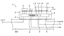
図1に示す回路モジュール1は、携帯電話や携帯情報端末などの通信携帯端末が備えるマザー基板MBに搭載されるものであり、この実施形態では、実装用基板2と、分波器10と、スイッチICやフィルタ、抵抗、コンデンサ、コイルなどの各種の部品3とを備え、高周波アンテナスイッチモジュールとして形成されている。また、分波器10および部品3は、実装用基板2の実装面2aに設けられた電極に実装されて、実装用基板2に設けられた内部配線パターン5を介して実装用基板2の裏面に形成された複数の実装用電極6に電気的に接続される。そして、回路モジュール1がマザー基板MBに実装されることにより、マザー基板MBが備えるアンテナラインANTやグランドラインGND、送信信号ラインTx、受信信号ラインRxなどの各種信号ラインおよび電源ラインと回路モジュール1とが接続されて、マザー基板MBと回路モジュール1との間で送受信信号の入出力が行われる。 (Circuit module)
Acircuit module 1 shown in FIG. 1 is mounted on a mother board MB provided in a communication portable terminal such as a mobile phone or a portable information terminal. In this embodiment, a mounting board 2, a duplexer 10, It includes various components 3 such as a switch IC, a filter, a resistor, a capacitor, and a coil, and is formed as a high frequency antenna switch module. Further, the duplexer 10 and the component 3 are mounted on electrodes provided on the mounting surface 2 a of the mounting substrate 2, and the back surface of the mounting substrate 2 through the internal wiring pattern 5 provided on the mounting substrate 2. Are electrically connected to the plurality of mounting electrodes 6. When the circuit module 1 is mounted on the mother board MB, various signal lines such as the antenna line ANT, the ground line GND, the transmission signal line Tx, the reception signal line Rx, and the power supply line provided in the mother board MB and the circuit module 1 Are connected, and transmission / reception signals are input / output between the mother board MB and the circuit module 1.
図1に示す回路モジュール1は、携帯電話や携帯情報端末などの通信携帯端末が備えるマザー基板MBに搭載されるものであり、この実施形態では、実装用基板2と、分波器10と、スイッチICやフィルタ、抵抗、コンデンサ、コイルなどの各種の部品3とを備え、高周波アンテナスイッチモジュールとして形成されている。また、分波器10および部品3は、実装用基板2の実装面2aに設けられた電極に実装されて、実装用基板2に設けられた内部配線パターン5を介して実装用基板2の裏面に形成された複数の実装用電極6に電気的に接続される。そして、回路モジュール1がマザー基板MBに実装されることにより、マザー基板MBが備えるアンテナラインANTやグランドラインGND、送信信号ラインTx、受信信号ラインRxなどの各種信号ラインおよび電源ラインと回路モジュール1とが接続されて、マザー基板MBと回路モジュール1との間で送受信信号の入出力が行われる。 (Circuit module)
A
実装用基板2は、この実施形態では、セラミックグリーンシートにより形成された複数の誘電体層が積層されて焼成されることで一体的にセラミック積層体として形成されており、各誘電体層に、ビア導体および電極パターンが適宜形成されることで内部配線パターン5が形成されている。
In this embodiment, the mounting substrate 2 is integrally formed as a ceramic laminate by laminating and firing a plurality of dielectric layers formed of ceramic green sheets. In each dielectric layer, The internal wiring pattern 5 is formed by appropriately forming via conductors and electrode patterns.
すなわち、各誘電体層を形成するセラミックグリーンシートは、アルミナおよびガラスなどの混合粉末が有機バインダおよび溶剤などと一緒に混合されたスラリーが成膜装置によりシート化されたものであり、約1000℃前後の低い温度で、所謂、低温焼成できるように形成されている。そして、所定形状に切り取られたセラミックグリーンシートに、レーザー加工などによりビアホールが形成され、形成されたビアホールにAgやCuなどを含む導体ペーストが充填されたり、ビアフィルめっきが施されることにより層間接続用のビア導体が形成され、導体ペーストによる印刷により種々の電極パターンが形成されて、各誘電体層が形成される。
That is, the ceramic green sheet forming each dielectric layer is a sheet in which a slurry in which a mixed powder such as alumina and glass is mixed with an organic binder and a solvent is formed into a sheet by a film forming apparatus. It is formed so that it can be fired at a low temperature before and after, so-called low temperature firing. Then, via holes are formed in the ceramic green sheet cut into a predetermined shape by laser processing or the like, and the formed via holes are filled with a conductive paste containing Ag, Cu, etc. Via conductors are formed, various electrode patterns are formed by printing with a conductive paste, and each dielectric layer is formed.
なお、内部配線パターン5は、回路モジュール1に実装される分波器10および各種部品3と、実装用電極6とを相互に電気的に接続するための電極パターンおよびビア導体が、各誘電体層に設けられることで形成される。このとき、内部配線パターン5を形成する電極パターンおよびビア導体によりコンデンサやコイルなどの回路素子を形成したり、電極パターンおよびビア導体によるコンデンサやコイルなどの回路素子によりフィルタ回路や整合回路などを形成してもよい。
The internal wiring pattern 5 includes an electrode pattern and a via conductor for electrically connecting the duplexer 10 and various components 3 mounted on the circuit module 1 and the mounting electrode 6 to each other. It is formed by being provided in the layer. At this time, a circuit element such as a capacitor or a coil is formed by the electrode pattern and via conductor forming the internal wiring pattern 5, or a filter circuit or a matching circuit is formed by the circuit element such as a capacitor or coil by the electrode pattern and via conductor. May be.
(分波器)
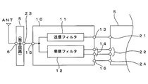
分波器10は、周波数の異なる送信信号と受信信号とを分離するために用いられるものであり、図2に示すように、分波器10は、高周波信号の通過帯域が異なる送信フィルタ11および受信フィルタ12を備えている。送信フィルタ11および受信フィルタ12は、それぞれSAW(表面弾性波)フィルタ素子により形成されており、この実施形態では、平衡出力型の受信フィルタ12が設けられている。なお、送信フィルタ11および受信フィルタ12としては、誘電体フィルタやBAWフィルタ素子など、所定帯域の信号を通過させる機能を有する素子であれば何でも構わない。 (Demultiplexer)
Theduplexer 10 is used to separate a transmission signal and a reception signal having different frequencies. As illustrated in FIG. 2, the duplexer 10 includes a transmission filter 11 and a high-frequency signal having different passbands. A reception filter 12 is provided. The transmission filter 11 and the reception filter 12 are each formed by a SAW (surface acoustic wave) filter element. In this embodiment, a balanced output type reception filter 12 is provided. The transmission filter 11 and the reception filter 12 may be any element as long as it has a function of passing a signal in a predetermined band, such as a dielectric filter or a BAW filter element.
分波器10は、周波数の異なる送信信号と受信信号とを分離するために用いられるものであり、図2に示すように、分波器10は、高周波信号の通過帯域が異なる送信フィルタ11および受信フィルタ12を備えている。送信フィルタ11および受信フィルタ12は、それぞれSAW(表面弾性波)フィルタ素子により形成されており、この実施形態では、平衡出力型の受信フィルタ12が設けられている。なお、送信フィルタ11および受信フィルタ12としては、誘電体フィルタやBAWフィルタ素子など、所定帯域の信号を通過させる機能を有する素子であれば何でも構わない。 (Demultiplexer)
The
また、分波器10は、送信フィルタ11への入力用の送信端子13と、受信フィルタ12からの出力用の受信端子14と、送信フィルタ12の出力側および受信フィルタ12の入力側に接続される共通端子15(アンテナ端子)と、接地端子16とを有し、実装用基板2に設けられた送信電極21、受信電極22、共通電極23および接地電極24とそれぞれ接続される。
The duplexer 10 is connected to the transmission terminal 13 for input to the transmission filter 11, the reception terminal 14 for output from the reception filter 12, the output side of the transmission filter 12, and the input side of the reception filter 12. The common terminal 15 (antenna terminal) and the ground terminal 16 are connected to the transmission electrode 21, the reception electrode 22, the common electrode 23, and the ground electrode 24 provided on the mounting substrate 2, respectively.
なお、この実施形態では、分波器10が備える送信フィルタ11および受信フィルタ12はSAWフィルタ素子により形成されているが、SAWフィルタ素子の他に、複数の共振器およびコイルなどが接続されて送信フィルタ11および受信フィルタ12が形成されていてもよく、周波数の異なる送信信号と受信信号とを確実に分波することができれば、送信フィルタ11および受信フィルタ12は、誘電体フィルタやBAWフィルタ素子など、どのようなものであってもよい。また、分波器10は、送信フィルタ11および受信フィルタ12を備える一般的なものを採用すればよく、その構成および動作は周知のものであるため、分波器10の構成および動作の詳細な説明は省略する。
In this embodiment, the transmission filter 11 and the reception filter 12 included in the duplexer 10 are formed by SAW filter elements. However, in addition to the SAW filter elements, a plurality of resonators, coils, and the like are connected for transmission. The filter 11 and the reception filter 12 may be formed. If the transmission signal and the reception signal having different frequencies can be reliably demultiplexed, the transmission filter 11 and the reception filter 12 may be a dielectric filter, a BAW filter element, or the like. Anything is acceptable. Further, as the duplexer 10, a general filter including the transmission filter 11 and the reception filter 12 may be adopted, and the configuration and operation thereof are well known, and therefore the configuration and operation of the duplexer 10 are detailed. Description is omitted.
(実装用基板の電極形状)
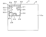
次に、図3を参照して、実装用基板2に設けられた送信電極21、受信電極22、共通電極23および接地電極24の電極形状の一例について説明する。 (Electrode shape of mounting board)
Next, an example of electrode shapes of thetransmission electrode 21, the reception electrode 22, the common electrode 23, and the ground electrode 24 provided on the mounting substrate 2 will be described with reference to FIG.
次に、図3を参照して、実装用基板2に設けられた送信電極21、受信電極22、共通電極23および接地電極24の電極形状の一例について説明する。 (Electrode shape of mounting board)
Next, an example of electrode shapes of the
図3に示すように、この実施形態では、実装用基板2を形成する複数の誘電体層の最上層の実装面2aに、送信電極21と、受信電極22と、共通電極23とが、矩形のランド状に設けられている。また、接地電極24は、実装面2aが設けられた誘電体層の1つ下層の誘電体層の表面に設けられており、接地電極24は、上面視において送信電極21および受信電極22の間に配置されている。
As shown in FIG. 3, in this embodiment, a transmission electrode 21, a reception electrode 22, and a common electrode 23 are rectangular on the uppermost mounting surface 2 a of a plurality of dielectric layers forming the mounting substrate 2. It is provided in the shape of a land. The ground electrode 24 is provided on the surface of the dielectric layer one layer below the dielectric layer provided with the mounting surface 2a, and the ground electrode 24 is located between the transmission electrode 21 and the reception electrode 22 in a top view. Are arranged.
また、この実施形態では、送信電極21および受信電極22は、実装用基板2の実装面2aの端縁2b近傍に設けられており、接地電極24は、端縁2b側の端部が該端縁2bに沿って両側に延出されて上面視において略T字状に形成されることにより、端縁2bと、送信電極21および受信電極22との間にも配置されている。また、接地電極24は、上面視において送信電極21、受信電極22および共通電極23それぞれの3辺を囲んで設けられている。すなわち、この実施形態では、接地電極24は、矩形の3辺にそれぞれ矩形状の切欠きが設けられた形状を成し、送信電極21、受信電極22および共通電極23は、上面視において、接地電極24に設けられた3つの矩形状の切欠きにそれぞれ配置されている。
In this embodiment, the transmission electrode 21 and the reception electrode 22 are provided in the vicinity of the edge 2b of the mounting surface 2a of the mounting substrate 2, and the end of the ground electrode 24 on the edge 2b side is the end. By extending to both sides along the edge 2 b and forming a substantially T shape in a top view, the edge 2 b is also disposed between the transmission electrode 21 and the reception electrode 22. The ground electrode 24 is provided so as to surround three sides of the transmission electrode 21, the reception electrode 22, and the common electrode 23 in a top view. That is, in this embodiment, the ground electrode 24 has a shape in which a rectangular cutout is provided on each of the three sides of the rectangle, and the transmission electrode 21, the reception electrode 22, and the common electrode 23 are grounded in a top view. They are arranged in three rectangular cutouts provided in the electrode 24, respectively.
また、接地電極24は、内部配線パターン5の複数のビア導体25が接続されることにより、マザー基板MBのグランドラインGNDと接続される実装用電極6と接続される。この実施形態では、特に、上面視において、接地電極24の送信電極21に近接する縁部に沿って複数のビア導体25が接続されている。また、この実施形態では、上面視において、接地電極24の送信電極21に近接する縁部から受信電極22に近接する縁部まで、接地電極24の縁部に沿って複数のビア導体25が接続されている。
The ground electrode 24 is connected to the mounting electrode 6 connected to the ground line GND of the mother board MB by connecting the plurality of via conductors 25 of the internal wiring pattern 5. In this embodiment, in particular, the plurality of via conductors 25 are connected along the edge portion of the ground electrode 24 close to the transmission electrode 21 in a top view. In this embodiment, a plurality of via conductors 25 are connected along the edge of the ground electrode 24 from the edge of the ground electrode 24 close to the transmission electrode 21 to the edge of the ground electrode 24 close to the reception electrode 22 in a top view. Has been.
なお、図3では、説明が容易となるように、送信電極21、受信電極22、共通電極23および接地電極24、並びに、接地電極24に接続されたビア導体25のみが図示されており、その他の電極およびビア導体25は図示省略されている。また、図3では、実装用基板2の内部に設けられた接地電極24およびビア導体25も実線で示されており、同図中の点線は、分波器10の実装面2aへの実装位置を示す。また、分波器10の接地端子16は、実装面2aに設けられた実装用の電極と、この電極に接続されるビア導体とを介して接地電極24と接続される(図示省略)。なお、後の説明で用いられる図4~図6においても図3と同様に図示されているため、以下ではその説明は省略する。
In FIG. 3, only the transmitting electrode 21, the receiving electrode 22, the common electrode 23, the ground electrode 24, and the via conductor 25 connected to the ground electrode 24 are shown for ease of explanation. The electrodes and via conductors 25 are not shown. In FIG. 3, the ground electrode 24 and the via conductor 25 provided inside the mounting substrate 2 are also shown by solid lines, and the dotted line in FIG. 3 indicates the mounting position on the mounting surface 2 a of the duplexer 10. Indicates. Further, the ground terminal 16 of the duplexer 10 is connected to the ground electrode 24 via a mounting electrode provided on the mounting surface 2a and a via conductor connected to the electrode (not shown). 4 to 6 used in the following description are also illustrated in the same manner as in FIG. 3, and the description thereof will be omitted below.
(製造方法)
次に、図1の回路モジュール1の製造方法の一例についてその概略を説明する。 (Production method)
Next, an outline of an example of a method for manufacturing thecircuit module 1 of FIG. 1 will be described.
次に、図1の回路モジュール1の製造方法の一例についてその概略を説明する。 (Production method)
Next, an outline of an example of a method for manufacturing the
まず、所定形状に形成されたセラミックグリーンシートに、レーザーなどでビアホールを形成し、内部に導体ペーストを充填したり、ビアフィルめっきを施すことにより層間接続用のビア導体25が形成され、送信電極21、受信電極22、共通電極23および接地電極24などの電極パターンが導体ペーストにより印刷されて、実装用基板2を構成する各誘電体層を形成するためのセラミックグリーンシートが準備される。なお、それぞれのセラミックグリーンシートには、一度に大量の実装用基板2を形成できるように、ビア導体25や、送信電極21、受信電極22、共通電極23および接地電極24などの電極パターンが複数設けられている。
First, a via hole is formed in a ceramic green sheet formed in a predetermined shape with a laser or the like, and a conductor paste is filled inside or via fill plating is performed to form a via conductor 25 for interlayer connection. Electrode patterns such as the reception electrode 22, the common electrode 23, and the ground electrode 24 are printed with a conductive paste, and a ceramic green sheet for forming each dielectric layer constituting the mounting substrate 2 is prepared. Each ceramic green sheet has a plurality of electrode patterns such as via conductors 25, transmission electrodes 21, reception electrodes 22, common electrodes 23, and ground electrodes 24 so that a large number of mounting substrates 2 can be formed at one time. Is provided.
次に、各誘電体層が積層されて積層体が形成される。そして、焼成後に個々の実装用基板2に分割するための溝が、各実装用基板2の領域を囲むように形成される。続いて、積層体が低温焼成されることにより実装用基板2の集合体が形成される。
Next, each dielectric layer is laminated to form a laminate. And the groove | channel for dividing | segmenting into each mounting board | substrate 2 after baking is formed so that the area | region of each mounting board | substrate 2 may be enclosed. Subsequently, the assembly of the mounting substrate 2 is formed by firing the laminated body at a low temperature.
次に、個々の実装用基板2に分割される前に、実装用基板2の集合体の実装面2aに分波器10および部品3が実装され、分波器10および部品3が実装された実装用基板2の集合体の実装面2aにモールド樹脂が充填されて、これが加熱硬化されることによりモールド層(図示省略)が各実装用基板2に設けられて回路モジュール1の集合体が形成される。そして、回路モジュール1の集合体は個々に分割されて、回路モジュール1が完成する。
Next, before being divided into individual mounting substrates 2, the duplexer 10 and the component 3 are mounted on the mounting surface 2a of the assembly of the mounting substrates 2, and the duplexer 10 and the component 3 are mounted. The mounting surface 2a of the assembly of mounting substrates 2 is filled with a mold resin, and this is heated and cured, whereby a mold layer (not shown) is provided on each mounting substrate 2 to form an assembly of circuit modules 1. Is done. Then, the assembly of the circuit modules 1 is divided individually to complete the circuit module 1.
このように形成された回路モジュール1では、マザー基板MBの送信信号ラインTxから、実装用電極6および内部配線パターン5を介して分波器10の送信端子13に出力された送信信号は、送信フィルタ11に入力されて所定のフィルタ処理が施されて、共通端子15から実装用基板2側に出力され、内部配線パターン5(整合回路)および実装用電極6を介してマザー基板MBのアンテナラインANTに出力される。また、マザー基板MBのアンテナラインANTから、実装用電極6および内部配線パターン5(整合回路)を介して分波器10の共通端子15に入力された受信信号は、受信フィルタ12に入力されて所定のフィルタ処理が施されて、受信端子14から実装用基板2側に出力され、内部配線パターン5および実装用電極6を介してマザー基板MBの受信信号ラインRxに出力される。
In the circuit module 1 thus formed, the transmission signal output from the transmission signal line Tx of the mother board MB to the transmission terminal 13 of the duplexer 10 via the mounting electrode 6 and the internal wiring pattern 5 is transmitted. The signal is input to the filter 11, subjected to a predetermined filtering process, output from the common terminal 15 to the mounting board 2 side, and the antenna line of the mother board MB via the internal wiring pattern 5 (matching circuit) and the mounting electrode 6. Output to ANT. A reception signal input from the antenna line ANT of the mother board MB to the common terminal 15 of the duplexer 10 via the mounting electrode 6 and the internal wiring pattern 5 (matching circuit) is input to the reception filter 12. Predetermined filtering is performed, the signal is output from the receiving terminal 14 to the mounting substrate 2 side, and is output to the reception signal line Rx of the mother substrate MB via the internal wiring pattern 5 and the mounting electrode 6.
なお、内部配線パターン5が設けられた実装用基板2、分波器10、部品3およびモールド層を備える回路モジュール1は、上記した製造方法に限らず、周知の一般的な製造方法により形成すればよく、実装用基板2は、樹脂やセラミック、ポリマー材料などを用いた、プリント基板、LTCC、アルミナ系基板、ガラス基板、複合材料基板、単層基板、多層基板などで形成することができ、回路モジュール1の使用目的に応じて、適宜最適な材質を選択して実装用基板2を形成すればよい。
The circuit module 1 including the mounting substrate 2 provided with the internal wiring pattern 5, the duplexer 10, the component 3, and the mold layer is not limited to the above-described manufacturing method, and may be formed by a known general manufacturing method. The mounting board 2 can be formed of a printed board, LTCC, alumina-based board, glass board, composite material board, single-layer board, multilayer board, etc. using resin, ceramic, polymer material, etc. The mounting substrate 2 may be formed by selecting an appropriate material as appropriate according to the purpose of use of the circuit module 1.
また、この実施形態では、内部配線パターン5により整合回路を形成したが、実装用基板2の実装面2aに実装されるチップコイルなどの部品3により整合回路を形成してもよい。
In this embodiment, the matching circuit is formed by the internal wiring pattern 5, but the matching circuit may be formed by a component 3 such as a chip coil mounted on the mounting surface 2 a of the mounting substrate 2.
以上のように、この実施形態では、分波器10は、送信フィルタ11への入力用の送信端子13と、受信フィルタ12からの出力用の受信端子14と、接地端子16とを有し、分波器10が実装される実装用基板2には、分波器10の送信端子13と接続される送信電極21と、分波器10の受信端子14と接続される受信電極22と、上面視において送信電極21および受信電極22の間に配置されて、分波器10の接地端子16と接続される接地電極24とが設けられている。また、実装用基板2の接地電極24には、上面視において当該接地電極24の送信電極21に近接する縁部に沿って複数のビア導体25が接続されている。
As described above, in this embodiment, the duplexer 10 includes the transmission terminal 13 for input to the transmission filter 11, the reception terminal 14 for output from the reception filter 12, and the ground terminal 16. The mounting substrate 2 on which the duplexer 10 is mounted includes a transmission electrode 21 connected to the transmission terminal 13 of the duplexer 10, a reception electrode 22 connected to the reception terminal 14 of the duplexer 10, and an upper surface. A ground electrode 24 that is disposed between the transmission electrode 21 and the reception electrode 22 and is connected to the ground terminal 16 of the duplexer 10 is provided. A plurality of via conductors 25 are connected to the ground electrode 24 of the mounting substrate 2 along an edge portion of the ground electrode 24 that is close to the transmission electrode 21 in a top view.
したがって、実装用基板2の送信電極21から分波器10の送信端子13に出力された送信信号が接地電極24に漏洩しても、接地電極24に漏洩した送信信号は、当該接地電極24の送信電極21に近接する縁部に沿って接続されてマザー基板MBのグランドラインGNDと接続されるビア導体25に流れ込むため、送信電極21から出力されて接地電極24に漏洩した送信信号が、当該接地電極24の縁部を伝って受信電極22側へ回り込むのが防止され、送信電極21および受信電極22が、地電極24を介して漏洩した送信信号により電気的に結合するのが防止されるので、分波器10が搭載される実装用基板2に設けられた送信電極21および受信電極22間のアイソレーション特性の向上を図ることができる。
Therefore, even if the transmission signal output from the transmission electrode 21 of the mounting substrate 2 to the transmission terminal 13 of the duplexer 10 leaks to the ground electrode 24, the transmission signal leaked to the ground electrode 24 Since it flows into the via conductor 25 connected along the edge near the transmission electrode 21 and connected to the ground line GND of the mother board MB, the transmission signal output from the transmission electrode 21 and leaked to the ground electrode 24 It is prevented that it goes around the edge of the ground electrode 24 to the reception electrode 22 side, and the transmission electrode 21 and the reception electrode 22 are prevented from being electrically coupled by the transmission signal leaked through the ground electrode 24. Therefore, the isolation characteristic between the transmission electrode 21 and the reception electrode 22 provided on the mounting substrate 2 on which the duplexer 10 is mounted can be improved.
また、接地電極24には、上面視において当該接地電極24の送信電極21に近接する縁部から受信電極22に近接する縁部まで、当該接地電極の縁部に沿って複数のビア導体25が接続されているため、送信電極21から出力されて接地電極24に漏洩した送信信号が、当該接地電極24の縁部に沿って接続された複数のビア導体25により効率よく流れ込むことにより、接地電極24に漏洩した送信信号が、当該接地電極24の縁部を伝って受信電極22側への回り込むのがより効率よく防止されるので、分波器10が搭載される実装用基板2に設けられた送信電極21および受信電極22間のアイソレーション特性をさらに向上することができる。
The ground electrode 24 has a plurality of via conductors 25 along the edge of the ground electrode from the edge of the ground electrode 24 close to the transmission electrode 21 to the edge of the ground electrode 24 close to the reception electrode 22 in a top view. As a result, the transmission signal output from the transmission electrode 21 and leaked to the ground electrode 24 efficiently flows through the plurality of via conductors 25 connected along the edge of the ground electrode 24. Since the transmission signal leaked to 24 is more efficiently prevented from traveling around the edge of the ground electrode 24 to the reception electrode 22 side, it is provided on the mounting substrate 2 on which the duplexer 10 is mounted. Further, the isolation characteristic between the transmission electrode 21 and the reception electrode 22 can be further improved.
また、送信電極21および受信電極22が、実装用基板2の実装面2aの端縁2b近傍に設けられることにより、分波器10が実装用基板2の端に詰めて配置されて回路モジュール1の小型化を図ることができる。しかも、接地電極24は、上面視において実装用基板2の端縁2bと、送信電極21および受信電極22との間にも設けられているため、送信電極21から出力されて接地電極24に漏洩した送信信号は、特に送信電極21側において、実装用基板2の端縁2bと送信電極21との間に設けられた接地電極24の縁部に沿って接続された複数のビア導体25に流れ込み、接地電極24に漏洩した送信信号が、当該接地電極24の縁部を伝って受信電極22側へ回り込むのが防止されるので、回路モジュール1の小型化を図ることにより、実装用基板2に設けられた送信電極21と受信電極22との間隔が狭くなっても、送信電極21および受信電極22間の高アイソレーション特性を維持することができる。
Further, the transmission electrode 21 and the reception electrode 22 are provided in the vicinity of the edge 2b of the mounting surface 2a of the mounting board 2, so that the duplexer 10 is arranged close to the end of the mounting board 2 and the circuit module 1 is placed. Can be miniaturized. Moreover, since the ground electrode 24 is also provided between the edge 2 b of the mounting substrate 2 and the transmission electrode 21 and the reception electrode 22 in a top view, the ground electrode 24 is output from the transmission electrode 21 and leaks to the ground electrode 24. The transmitted signal flows into a plurality of via conductors 25 connected along the edge of the ground electrode 24 provided between the end edge 2b of the mounting substrate 2 and the transmission electrode 21, particularly on the transmission electrode 21 side. Since the transmission signal leaked to the ground electrode 24 is prevented from flowing around the edge of the ground electrode 24 to the receiving electrode 22 side, the circuit module 1 can be reduced in size, and the mounting substrate 2 can be reduced. Even if the interval between the provided transmission electrode 21 and the reception electrode 22 is narrow, high isolation characteristics between the transmission electrode 21 and the reception electrode 22 can be maintained.
また、送信電極21、受信電極22および共通電極23が、実装用基板2の実装面2aに矩形のランド状に設けられており、接地電極24は、上面視において送信電極21、受信電極22および共通電極23それぞれの少なくとも3辺を囲んで設けられているため、送信電極21から出力されて接地電極24に漏洩した送信信号は、送信電極21の少なくとも3辺を囲む当該接地電極24の縁部に沿って接続されたビア導体25に効率よく流れ込むと共に、上面視において当該接地電極24の送信電極21に近接する縁部から受信電極22に近接する縁部までの、当該接地電極24の縁部に沿った距離が長くなるので、接地電極24に漏洩した送信信号が、当該接地電極24の縁部を伝って受信電極24側へ回り込むのを確実に防止することができる。
Further, the transmission electrode 21, the reception electrode 22, and the common electrode 23 are provided in a rectangular land shape on the mounting surface 2a of the mounting substrate 2, and the ground electrode 24 is formed by transmitting the transmission electrode 21, the reception electrode 22, and the common electrode 23 in a top view. Since the common electrode 23 is provided so as to surround at least three sides, the transmission signal output from the transmission electrode 21 and leaked to the ground electrode 24 is an edge portion of the ground electrode 24 surrounding at least three sides of the transmission electrode 21. The edge portion of the ground electrode 24 from the edge portion close to the transmission electrode 21 of the ground electrode 24 to the edge portion close to the reception electrode 22 in a top view is efficiently flown into the via conductor 25 connected along As a result, the transmission signal leaked to the ground electrode 24 is reliably prevented from traveling around the edge of the ground electrode 24 toward the reception electrode 24. Can.
<第2実施形態>
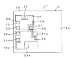
次に、図4を参照して本発明の第2実施形態について説明する。図4は本発明の第2実施形態における実装用基板の電極形状の一例を示す平面図である。この実施形態が上記した第1実施形態と異なる点は、図4に示すように、接地電極24に、上面視において、分波器10の外側に延出して設けられた延出部24a(本発明の「第1の延出部」に相当)が送信電極21および受信電極22側に設けられている点である。その他の構成は上記した第1実施形態と同様の構成であるため、同一符号を付すことによりその構成の説明は省略する。 Second Embodiment
Next, a second embodiment of the present invention will be described with reference to FIG. FIG. 4 is a plan view showing an example of the electrode shape of the mounting substrate according to the second embodiment of the present invention. As shown in FIG. 4, this embodiment is different from the first embodiment described above in that an extended portion 24 a (this one) is provided on theground electrode 24 so as to extend outside the duplexer 10 in a top view. (Corresponding to the “first extending portion” of the invention) is provided on the transmitting electrode 21 and receiving electrode 22 side. Since other configurations are the same as those in the first embodiment, description of the configuration is omitted by giving the same reference numerals.
次に、図4を参照して本発明の第2実施形態について説明する。図4は本発明の第2実施形態における実装用基板の電極形状の一例を示す平面図である。この実施形態が上記した第1実施形態と異なる点は、図4に示すように、接地電極24に、上面視において、分波器10の外側に延出して設けられた延出部24a(本発明の「第1の延出部」に相当)が送信電極21および受信電極22側に設けられている点である。その他の構成は上記した第1実施形態と同様の構成であるため、同一符号を付すことによりその構成の説明は省略する。 Second Embodiment
Next, a second embodiment of the present invention will be described with reference to FIG. FIG. 4 is a plan view showing an example of the electrode shape of the mounting substrate according to the second embodiment of the present invention. As shown in FIG. 4, this embodiment is different from the first embodiment described above in that an extended portion 24 a (this one) is provided on the
このように構成すると、接地電極24は、上面視において分波器10の外側に延出して設けられた延出部24aを備えているため、当該接地電極24の送信電極21に近接する縁部から受信電極22に近接する縁部までの、当該接地電極24の縁部に沿った距離が長くなるので、送信電極21から出力されて接地電極24に漏洩した送信信号が、当該接地電極24の縁部を伝って受信電極22側へ回り込むのを防止することができる。
If comprised in this way, since the ground electrode 24 is provided with the extension part 24a extended and provided in the outer side of the splitter 10 in the top view, the edge part which adjoins the transmission electrode 21 of the said ground electrode 24 Since the distance along the edge of the ground electrode 24 from the terminal to the edge close to the reception electrode 22 becomes long, the transmission signal output from the transmission electrode 21 and leaked to the ground electrode 24 It is possible to prevent the reception electrode 22 from going around along the edge.
なお、上面視において、接地電極24が、送信電極21または受信電極22の矩形の少なくとも2辺に近接配置されるように、接地電極24の延出部24aを、その端部から送信電極21および受信電極22の少なくとも一方の方向にさら延出してもよい(本発明の「第2の延出部」に相当)。このように構成すると、上面視において当該接地電極24の送信電極21に近接する縁部から受信電極22に近接する縁部までの、当該接地電極24の縁部に沿った距離がさらに長くなるので、送信電極21から出力されて接地電極24に漏洩した送信信号が、当該接地電極24の縁部を伝って受信電極22側へ回り込むのをより確実に防止することができる。
In addition, when viewed from the top, the extended portion 24a of the ground electrode 24 is arranged from the end thereof so that the ground electrode 24 is disposed close to at least two sides of the rectangular shape of the transmission electrode 21 or the reception electrode 22. It may extend further in at least one direction of the receiving electrode 22 (corresponding to the “second extending portion” of the present invention). With this configuration, the distance along the edge of the ground electrode 24 from the edge of the ground electrode 24 close to the transmission electrode 21 to the edge of the ground electrode 24 close to the reception electrode 22 in the top view is further increased. The transmission signal output from the transmission electrode 21 and leaked to the ground electrode 24 can be more reliably prevented from traveling around the edge of the ground electrode 24 toward the reception electrode 22 side.
<第3実施形態>
次に、図5を参照して本発明の第3実施形態について説明する。図5は本発明の第3実施形態における実装用基板の電極形状の一例を示す平面図である。この実施形態が上記した第1実施形態と異なる点は、図5に示すように、実装用基板2の実装面2aに2つの分波器10,10aが実装されており、実装面2aに、分波器10aが実装される送信電極21a、受信電極22aおよび共通電極23aがさらに設けられて、接地電極24が、送信電極21,21aと受信電極22,22aとの間に配置されるように大面積に形成されている点である。その他の構成は上記した第1実施形態と同様の構成であるため、同一符号を付すことによりその構成の説明は省略する。 <Third Embodiment>
Next, a third embodiment of the present invention will be described with reference to FIG. FIG. 5 is a plan view showing an example of the electrode shape of the mounting board according to the third embodiment of the present invention. This embodiment is different from the first embodiment described above in that twoduplexers 10 and 10a are mounted on the mounting surface 2a of the mounting board 2 as shown in FIG. A transmission electrode 21a on which the duplexer 10a is mounted, a reception electrode 22a, and a common electrode 23a are further provided, and the ground electrode 24 is disposed between the transmission electrodes 21 and 21a and the reception electrodes 22 and 22a. It is a point formed in a large area. Since other configurations are the same as those in the first embodiment, description of the configuration is omitted by giving the same reference numerals.
次に、図5を参照して本発明の第3実施形態について説明する。図5は本発明の第3実施形態における実装用基板の電極形状の一例を示す平面図である。この実施形態が上記した第1実施形態と異なる点は、図5に示すように、実装用基板2の実装面2aに2つの分波器10,10aが実装されており、実装面2aに、分波器10aが実装される送信電極21a、受信電極22aおよび共通電極23aがさらに設けられて、接地電極24が、送信電極21,21aと受信電極22,22aとの間に配置されるように大面積に形成されている点である。その他の構成は上記した第1実施形態と同様の構成であるため、同一符号を付すことによりその構成の説明は省略する。 <Third Embodiment>
Next, a third embodiment of the present invention will be described with reference to FIG. FIG. 5 is a plan view showing an example of the electrode shape of the mounting board according to the third embodiment of the present invention. This embodiment is different from the first embodiment described above in that two
このように構成すると、上記した第1実施形態と同様の効果を奏することができる。
With this configuration, the same effects as those of the first embodiment described above can be obtained.
<第4実施形態>
次に、図6を参照して本発明の第4実施形態について説明する。図6は本発明の第4実施形態における実装用基板の電極形状の一例を示す平面図である。この実施形態が上記した第3実施形態と異なる点は、図6に示すように、分波器10を実装するための送信電極21および受信電極22が、接地電極24の同図中の上下方向における中央側に配置され、共通電極23が接地電極24の上端側に配置されている点である。その他の構成は上記した第3実施形態と同様の構成であるため、同一符号を付すことによりその構成の説明は省略する。なお、図6では、接地電極24の送信電極21,21aに近接する縁部に沿って接続されたビア導体25のみが図示され、その他のビア導体25は図示省略されている。 <Fourth embodiment>
Next, a fourth embodiment of the present invention will be described with reference to FIG. FIG. 6 is a plan view showing an example of the electrode shape of the mounting board in the fourth embodiment of the present invention. This embodiment differs from the third embodiment described above in that, as shown in FIG. 6, the transmittingelectrode 21 and the receiving electrode 22 for mounting the duplexer 10 are arranged in the vertical direction of the ground electrode 24 in the figure. The common electrode 23 is arranged on the upper end side of the ground electrode 24. Since other configurations are the same as those in the third embodiment described above, description of the configurations is omitted by giving the same reference numerals. In FIG. 6, only the via conductor 25 connected along the edge portion of the ground electrode 24 close to the transmission electrodes 21 and 21a is shown, and the other via conductors 25 are not shown.
次に、図6を参照して本発明の第4実施形態について説明する。図6は本発明の第4実施形態における実装用基板の電極形状の一例を示す平面図である。この実施形態が上記した第3実施形態と異なる点は、図6に示すように、分波器10を実装するための送信電極21および受信電極22が、接地電極24の同図中の上下方向における中央側に配置され、共通電極23が接地電極24の上端側に配置されている点である。その他の構成は上記した第3実施形態と同様の構成であるため、同一符号を付すことによりその構成の説明は省略する。なお、図6では、接地電極24の送信電極21,21aに近接する縁部に沿って接続されたビア導体25のみが図示され、その他のビア導体25は図示省略されている。 <Fourth embodiment>
Next, a fourth embodiment of the present invention will be described with reference to FIG. FIG. 6 is a plan view showing an example of the electrode shape of the mounting board in the fourth embodiment of the present invention. This embodiment differs from the third embodiment described above in that, as shown in FIG. 6, the transmitting
このように構成すると、上面視において接地電極24の送信電極21,21aに近接する縁部から受信電極22,22aに近接する縁部までの、当該接地電極24の縁部に沿った距離が長くなり、上記した第1実施形態と同様の効果を奏することができる。
With this configuration, the distance along the edge of the ground electrode 24 from the edge of the ground electrode 24 near the transmitting electrodes 21 and 21a to the edge near the receiving electrodes 22 and 22a is long in a top view. Thus, the same effects as those of the first embodiment described above can be obtained.
なお、本発明は上記した実施形態に限定されるものではなく、その趣旨を逸脱しない限りにおいて、上記したもの以外に種々の変更を行なうことが可能である。例えば、接地電極24を、実装用基板2を構成する複数の誘電体層に渡って設け、各接地電極24を、複数のビア導体25で接続してもよい。
Note that the present invention is not limited to the above-described embodiment, and various modifications other than those described above can be made without departing from the spirit of the present invention. For example, the ground electrode 24 may be provided across a plurality of dielectric layers constituting the mounting substrate 2, and each ground electrode 24 may be connected by a plurality of via conductors 25.
このように構成すると、実装用基板2に複数層に渡って設けられた各接地電極24がビア導体25で接続されているため、送信電極21,21aから出力されて接地電極24に漏洩した送信信号は、上面視において、当該接地電極24の送信電極21,21aに近接する縁部に沿って接続された複数のビア導体25にさらに効率よく流れ込むので、接地電極24に漏洩した送信信号が、当該接地電極24の縁部を伝って受信電極22,22a側へ回り込むのをさらに効率よく防止でき、分波器10,10aが搭載される実装用基板に設けられた送信電極21,21aおよび受信電極22,22a間のアイソレーション特性をより一層向上することができる。
With this configuration, since the ground electrodes 24 provided in a plurality of layers on the mounting substrate 2 are connected by the via conductors 25, the transmission output from the transmission electrodes 21 and 21a and leaked to the ground electrode 24 Since the signal flows more efficiently into the plurality of via conductors 25 connected along the edge portions of the ground electrode 24 close to the transmission electrodes 21 and 21a in a top view, the transmission signal leaked to the ground electrode 24 is It is possible to more efficiently prevent the transmission electrode 21 and 22a from wrapping around the edge of the ground electrode 24 toward the reception electrodes 22 and 22a, and the transmission electrodes 21 and 21a and the reception provided on the mounting substrate on which the duplexers 10 and 10a are mounted. The isolation characteristic between the electrodes 22 and 22a can be further improved.
なお、実装用基板2に複数層に渡って設けられた各接地電極24は、同一形状であってもよいが、少なくとも、上面視において、送信電極21,21aに近接する部分の形状を同一にすることにより、送信電極21,21aから出力されて接地電極24に漏洩した送信信号を、当該接地電極24の縁部に沿って接続された複数のビア導体25に効率よく誘導することができる。
The ground electrodes 24 provided on the mounting substrate 2 over a plurality of layers may have the same shape, but at least the portions adjacent to the transmission electrodes 21 and 21a in the top view have the same shape. As a result, the transmission signal output from the transmission electrodes 21 and 21a and leaked to the ground electrode 24 can be efficiently guided to the plurality of via conductors 25 connected along the edge of the ground electrode 24.
また、接地電極24を、上面視において少なくとも送信電極21,21aを囲む形状に形成してもよい。このように構成すると、送信電極21,21aから出力されて接地電極24に漏洩した送信信号は、当該接地電極24の送信電極21,21aを囲む縁部に沿って接続されたビア導体25に流れ込むと共に、当該接地電極24の送信電極21,21aを囲む縁部と当該接地電極24の受信電極22,22aに近接する縁部とが連続していないため、接地電極24に漏洩した送信信号が、当該接地電極24の縁部を伝って受信電極22,22a側へ回り込むのを確実に防止することができる。
Further, the ground electrode 24 may be formed in a shape surrounding at least the transmission electrodes 21 and 21a in a top view. With this configuration, the transmission signal output from the transmission electrodes 21 and 21a and leaked to the ground electrode 24 flows into the via conductor 25 connected along the edge surrounding the transmission electrodes 21 and 21a of the ground electrode 24. At the same time, since the edge surrounding the transmission electrodes 21 and 21a of the ground electrode 24 and the edge of the ground electrode 24 adjacent to the reception electrodes 22 and 22a are not continuous, the transmission signal leaked to the ground electrode 24 is It is possible to reliably prevent wrapping around the receiving electrodes 22 and 22a along the edge of the ground electrode 24.
また、少なくとも、上面視において接地電極24の送信電極21,21aに近接する縁部に沿って複数のビア導体25が接続されていればよく、接地電極24を実装用基板2の実装面2aに設けてもよい。
In addition, at least a plurality of via conductors 25 may be connected along the edge portion of the ground electrode 24 close to the transmission electrodes 21 and 21a when viewed from above, and the ground electrode 24 is connected to the mounting surface 2a of the mounting substrate 2. It may be provided.
また、実装用基板2の実装面2aに設けられる、送信電極21,21a、受信電極22,22aおよび共通電極23a,23aの形状は矩形状に限られるものではなく、円形状など、分波器10,10aを実装することができれば、どのような形状であってもよく、接地電極24は、必ずしも、矩形状の送信電極21,21a、受信電極22,22aおよび共通電極23a,23aを、少なくとも3方向から囲むように形成しなくともよい。
Further, the shapes of the transmission electrodes 21 and 21a, the reception electrodes 22 and 22a, and the common electrodes 23a and 23a provided on the mounting surface 2a of the mounting substrate 2 are not limited to rectangular shapes, The ground electrode 24 is not necessarily limited to the rectangular transmission electrodes 21 and 21a, the reception electrodes 22 and 22a, and the common electrodes 23a and 23a. It does not have to be formed so as to surround from three directions.
本発明は、通過帯域が異なる送信フィルタおよび受信フィルタを有する分波器を備える回路モジュールに本発明を広く適用することができる。
The present invention can be widely applied to a circuit module including a duplexer having a transmission filter and a reception filter having different passbands.
1 回路モジュール
2 実装用基板
2a 実装面
2b 端縁
10,10a 分波器
11 送信フィルタ
12 受信フィルタ
13 送信端子
14 受信端子
15 共通端子
16 接地端子
21,21a 送信電極
22,22a 受信電極
23,23a 共通電極
24 接地電極
24a 延出部(第1の延出部)
25 ビア導体 DESCRIPTION OFSYMBOLS 1 Circuit module 2 Mounting board 2a Mounting surface 2b Edge 10, 10a Splitter 11 Transmission filter 12 Reception filter 13 Transmission terminal 14 Reception terminal 15 Common terminal 16 Ground terminal 21, 21a Transmission electrode 22, 22a Reception electrode 23, 23a Common electrode 24 Ground electrode 24a Extension part (first extension part)
25 Via conductor
2 実装用基板
2a 実装面
2b 端縁
10,10a 分波器
11 送信フィルタ
12 受信フィルタ
13 送信端子
14 受信端子
15 共通端子
16 接地端子
21,21a 送信電極
22,22a 受信電極
23,23a 共通電極
24 接地電極
24a 延出部(第1の延出部)
25 ビア導体 DESCRIPTION OF
25 Via conductor
Claims (9)
- 通過帯域が異なる送信フィルタおよび受信フィルタを有する分波器を備える回路モジュールにおいて、
前記分波器が実装される実装用基板を備え、
前記分波器は、前記送信フィルタへの入力用の送信端子と、前記受信フィルタからの出力用の受信端子と、接地端子とを有し、
前記実装用基板には、前記送信端子と接続される送信電極と、前記受信端子と接続される受信電極と、上面視において前記送信電極および前記受信電極の間に配置されて前記接地端子と接続される接地電極とが設けられており、
前記接地電極には、上面視において当該接地電極の前記送信電極に近接する縁部に沿って複数のビア導体が接続されている
ことを特徴とする回路モジュール。 In a circuit module including a duplexer having a transmission filter and a reception filter having different passbands,
A mounting substrate on which the duplexer is mounted;
The duplexer has a transmission terminal for input to the transmission filter, a reception terminal for output from the reception filter, and a ground terminal,
The mounting substrate has a transmission electrode connected to the transmission terminal, a reception electrode connected to the reception terminal, and is disposed between the transmission electrode and the reception electrode in a top view and connected to the ground terminal And a ground electrode to be provided,
The circuit module, wherein a plurality of via conductors are connected to the ground electrode along an edge portion of the ground electrode close to the transmission electrode in a top view. - 前記接地電極には、上面視において当該接地電極の前記送信電極に近接する縁部から前記受信電極に近接する縁部まで、当該接地電極の縁部に沿って前記複数のビア導体が接続されていることを特徴とする請求項1に記載の回路モジュール。 The plurality of via conductors are connected to the ground electrode along an edge of the ground electrode from an edge of the ground electrode close to the transmission electrode to an edge of the ground electrode close to the reception electrode. The circuit module according to claim 1.
- 前記送信電極および前記受信電極は、前記実装用基板の実装面の端縁近傍に設けられており、前記接地電極は、上面視において前記端縁および前記送信電極の間に設けられていることを特徴とする請求項1または2に記載の回路モジュール。 The transmission electrode and the reception electrode are provided in the vicinity of an edge of the mounting surface of the mounting substrate, and the ground electrode is provided between the edge and the transmission electrode in a top view. The circuit module according to claim 1, wherein the circuit module is characterized in that:
- 前記接地電極は、前記実装用基板に複数層に渡って設けられており、前記各接地電極が前記ビア導体で接続されていることを特徴とする請求項1ないし3のいずれかに記載の回路モジュール。 4. The circuit according to claim 1, wherein the ground electrode is provided in a plurality of layers on the mounting substrate, and the ground electrodes are connected by the via conductor. module.
- 前記接地電極は、上面視において前記分波器の外側に延出して設けられた第1の延出部を備えていることを特徴とする請求項1ないし4のいずれかに記載の回路モジュール。 5. The circuit module according to claim 1, wherein the ground electrode includes a first extending portion provided to extend outside the duplexer in a top view.
- 前記接地電極は、前記第1の延出部の端部から前記送信電極および前記受信電極の少なくとも一方の方向にさら延出して設けられた第2の延出部をさらに備えていることを特徴とする請求項5に記載の回路モジュール。 The ground electrode further includes a second extension portion provided to extend from an end portion of the first extension portion in at least one direction of the transmission electrode and the reception electrode. The circuit module according to claim 5.
- 前記接地電極は、上面視において少なくとも前記送信電極を囲む形状に形成されていることを特徴とする請求項1ないし6のいずれかに記載の回路モジュール。 7. The circuit module according to claim 1, wherein the ground electrode is formed in a shape surrounding at least the transmission electrode in a top view.
- 前記送信電極および前記受信電極のうち少なくとも一方は、前記実装用基板の実装面に矩形のランド状に設けられており、前記接地電極は、矩形状に形成された前記送信電極または前記受信電極の少なくとも3辺を上面視において囲んで設けられていることを特徴とする請求項1ないし6のいずれかに記載の回路モジュール。 At least one of the transmission electrode and the reception electrode is provided in a rectangular land shape on the mounting surface of the mounting substrate, and the ground electrode is formed of the transmission electrode or the reception electrode formed in a rectangular shape. 7. The circuit module according to claim 1, wherein at least three sides are provided so as to surround the top view.
- 前記分波器は、前記送信フィルタの出力側および前記受信フィルタの入力側に接続される共通端子をさらに有し、
前記送信電極および前記受信電極と、前記共通端子と接続される共通電極とが、前記実装用基板の実装面に矩形のランド状に設けられており、
前記接地電極は、上面視において前記送信電極、前記受信電極および前記共通電極それぞれの少なくとも3辺を囲んで設けられていることを特徴とする請求項1ないし6のいずれかに記載の回路モジュール。 The duplexer further includes a common terminal connected to the output side of the transmission filter and the input side of the reception filter;
The transmission electrode and the reception electrode, and a common electrode connected to the common terminal are provided in a rectangular land shape on the mounting surface of the mounting substrate,
The circuit module according to claim 1, wherein the ground electrode is provided so as to surround at least three sides of each of the transmission electrode, the reception electrode, and the common electrode in a top view.
Priority Applications (3)
| Application Number | Priority Date | Filing Date | Title |
|---|---|---|---|
| CN201280019253.2A CN103493371B (en) | 2011-04-21 | 2012-04-20 | Circuit module |
| JP2013510897A JP5807675B2 (en) | 2011-04-21 | 2012-04-20 | Circuit module |
| US14/057,000 US9252476B2 (en) | 2011-04-21 | 2013-10-18 | Circuit module including a splitter and a mounting substrate |
Applications Claiming Priority (2)
| Application Number | Priority Date | Filing Date | Title |
|---|---|---|---|
| JP2011-095193 | 2011-04-21 | ||
| JP2011095193 | 2011-04-21 |
Related Child Applications (1)
| Application Number | Title | Priority Date | Filing Date |
|---|---|---|---|
| US14/057,000 Continuation US9252476B2 (en) | 2011-04-21 | 2013-10-18 | Circuit module including a splitter and a mounting substrate |
Publications (1)
| Publication Number | Publication Date |
|---|---|
| WO2012144228A1 true WO2012144228A1 (en) | 2012-10-26 |
Family
ID=47041357
Family Applications (1)
| Application Number | Title | Priority Date | Filing Date |
|---|---|---|---|
| PCT/JP2012/002741 WO2012144228A1 (en) | 2011-04-21 | 2012-04-20 | Circuit module |
Country Status (4)
| Country | Link |
|---|---|
| US (1) | US9252476B2 (en) |
| JP (1) | JP5807675B2 (en) |
| CN (1) | CN103493371B (en) |
| WO (1) | WO2012144228A1 (en) |
Cited By (3)
| Publication number | Priority date | Publication date | Assignee | Title |
|---|---|---|---|---|
| CN104854792A (en) * | 2013-10-17 | 2015-08-19 | 株式会社村田制作所 | High-frequency circuit module |
| DE102015002297A1 (en) | 2015-02-23 | 2016-08-25 | MAX-PLANCK-Gesellschaft zur Förderung der Wissenschaften e.V. | Rope robot system for motion simulation |
| WO2022163409A1 (en) * | 2021-01-29 | 2022-08-04 | 株式会社村田製作所 | High frequency module and communication device |
Families Citing this family (6)
| Publication number | Priority date | Publication date | Assignee | Title |
|---|---|---|---|---|
| JP6544981B2 (en) * | 2015-04-20 | 2019-07-17 | ローム株式会社 | Printed wiring board |
| US9660609B2 (en) * | 2015-07-07 | 2017-05-23 | Skyworks Solutions, Inc. | Devices and methods related to stacked duplexers |
| CN105810666A (en) * | 2016-03-30 | 2016-07-27 | 江苏长电科技股份有限公司 | Fabrication method for package structure having electromagnetic shielding function |
| CN109067380A (en) * | 2018-07-11 | 2018-12-21 | 深圳振华富电子有限公司 | Antivibration dynamic formula power splitter |
| CN209402820U (en) * | 2018-10-31 | 2019-09-17 | 惠科股份有限公司 | Circuit board and display device |
| US11457524B2 (en) * | 2019-04-29 | 2022-09-27 | Nxp B.V. | Integrated filter for de-sense reduction |
Citations (6)
| Publication number | Priority date | Publication date | Assignee | Title |
|---|---|---|---|---|
| JPH09121137A (en) * | 1996-09-30 | 1997-05-06 | Hitachi Ltd | Surface acoustic wave device and equipment using the same |
| JP2003152292A (en) * | 2001-11-19 | 2003-05-23 | Kyocera Corp | Wiring board |
| JP2003273277A (en) * | 2002-03-14 | 2003-09-26 | Fujitsu Ltd | High-frequency integrated circuit module |
| JP2003298462A (en) * | 2002-04-01 | 2003-10-17 | Ngk Spark Plug Co Ltd | Ceramic board for branching filter device |
| WO2009104251A1 (en) * | 2008-02-20 | 2009-08-27 | 富士通株式会社 | Filter, branching filter, communication module, and communication equipment |
| WO2010067497A1 (en) * | 2008-12-10 | 2010-06-17 | 株式会社村田製作所 | High-frequency module |
Family Cites Families (5)
| Publication number | Priority date | Publication date | Assignee | Title |
|---|---|---|---|---|
| JPH0514015A (en) | 1991-07-03 | 1993-01-22 | Tdk Corp | High frequency smd module |
| JPH0745746A (en) | 1993-07-30 | 1995-02-14 | Toshiba Lighting & Technol Corp | Hybrid high-frequency wave attenuator circuit |
| JP3180774B2 (en) | 1998-08-31 | 2001-06-25 | 日本電気株式会社 | High frequency amplifier |
| JP2006279604A (en) | 2005-03-29 | 2006-10-12 | Tdk Corp | Surface acoustic wave device |
| JP4943137B2 (en) * | 2006-12-25 | 2012-05-30 | 京セラ株式会社 | Duplexer and communication device |
-
2012
- 2012-04-20 WO PCT/JP2012/002741 patent/WO2012144228A1/en active Application Filing
- 2012-04-20 CN CN201280019253.2A patent/CN103493371B/en active Active
- 2012-04-20 JP JP2013510897A patent/JP5807675B2/en active Active
-
2013
- 2013-10-18 US US14/057,000 patent/US9252476B2/en active Active
Patent Citations (6)
| Publication number | Priority date | Publication date | Assignee | Title |
|---|---|---|---|---|
| JPH09121137A (en) * | 1996-09-30 | 1997-05-06 | Hitachi Ltd | Surface acoustic wave device and equipment using the same |
| JP2003152292A (en) * | 2001-11-19 | 2003-05-23 | Kyocera Corp | Wiring board |
| JP2003273277A (en) * | 2002-03-14 | 2003-09-26 | Fujitsu Ltd | High-frequency integrated circuit module |
| JP2003298462A (en) * | 2002-04-01 | 2003-10-17 | Ngk Spark Plug Co Ltd | Ceramic board for branching filter device |
| WO2009104251A1 (en) * | 2008-02-20 | 2009-08-27 | 富士通株式会社 | Filter, branching filter, communication module, and communication equipment |
| WO2010067497A1 (en) * | 2008-12-10 | 2010-06-17 | 株式会社村田製作所 | High-frequency module |
Cited By (4)
| Publication number | Priority date | Publication date | Assignee | Title |
|---|---|---|---|---|
| CN104854792A (en) * | 2013-10-17 | 2015-08-19 | 株式会社村田制作所 | High-frequency circuit module |
| US9883585B2 (en) | 2013-10-17 | 2018-01-30 | Murata Manufacturing Co., Ltd. | Radio-frequency circuit module |
| DE102015002297A1 (en) | 2015-02-23 | 2016-08-25 | MAX-PLANCK-Gesellschaft zur Förderung der Wissenschaften e.V. | Rope robot system for motion simulation |
| WO2022163409A1 (en) * | 2021-01-29 | 2022-08-04 | 株式会社村田製作所 | High frequency module and communication device |
Also Published As
| Publication number | Publication date |
|---|---|
| US9252476B2 (en) | 2016-02-02 |
| US20140045546A1 (en) | 2014-02-13 |
| CN103493371B (en) | 2016-11-09 |
| JPWO2012144228A1 (en) | 2014-07-28 |
| JP5807675B2 (en) | 2015-11-10 |
| CN103493371A (en) | 2014-01-01 |
Similar Documents
| Publication | Publication Date | Title |
|---|---|---|
| JP5807675B2 (en) | Circuit module | |
| US9178491B2 (en) | Circuit module including duplexer | |
| US10454446B2 (en) | High-frequency module | |
| JP6489182B2 (en) | Wireless module with integrated antenna | |
| JP5677499B2 (en) | High frequency circuit module | |
| KR101622452B1 (en) | Module substrate and module | |
| US8963652B2 (en) | Duplexer and circuit module including the same | |
| JP5672412B2 (en) | Compound module | |
| JP5618003B2 (en) | Circuit module | |
| WO2013011649A1 (en) | Demultiplexer | |
| WO2014013831A1 (en) | Module and module manufacturing method | |
| JP2006211144A (en) | High frequency module and wireless communication apparatus | |
| JP5420102B1 (en) | High frequency circuit module | |
| JP5420103B1 (en) | High frequency circuit module | |
| JP2014039265A (en) | High-frequency circuit module |
Legal Events
| Date | Code | Title | Description |
|---|---|---|---|
| 121 | Ep: the epo has been informed by wipo that ep was designated in this application |
Ref document number: 12774199 Country of ref document: EP Kind code of ref document: A1 |
|
| ENP | Entry into the national phase |
Ref document number: 2013510897 Country of ref document: JP Kind code of ref document: A |
|
| NENP | Non-entry into the national phase |
Ref country code: DE |
|
| 122 | Ep: pct application non-entry in european phase |
Ref document number: 12774199 Country of ref document: EP Kind code of ref document: A1 |