WO2012133285A1 - 信号処理装置、制御プログラム、および集積回路 - Google Patents
信号処理装置、制御プログラム、および集積回路 Download PDFInfo
- Publication number
- WO2012133285A1 WO2012133285A1 PCT/JP2012/057716 JP2012057716W WO2012133285A1 WO 2012133285 A1 WO2012133285 A1 WO 2012133285A1 JP 2012057716 W JP2012057716 W JP 2012057716W WO 2012133285 A1 WO2012133285 A1 WO 2012133285A1
- Authority
- WO
- WIPO (PCT)
- Prior art keywords
- signal
- block
- boundary
- frequency
- block boundary
- Prior art date
- Legal status (The legal status is an assumption and is not a legal conclusion. Google has not performed a legal analysis and makes no representation as to the accuracy of the status listed.)
- Ceased
Links
Images








Classifications
-
- G—PHYSICS
- G06—COMPUTING OR CALCULATING; COUNTING
- G06T—IMAGE DATA PROCESSING OR GENERATION, IN GENERAL
- G06T5/00—Image enhancement or restoration
- G06T5/70—Denoising; Smoothing
-
- H—ELECTRICITY
- H04—ELECTRIC COMMUNICATION TECHNIQUE
- H04N—PICTORIAL COMMUNICATION, e.g. TELEVISION
- H04N19/00—Methods or arrangements for coding, decoding, compressing or decompressing digital video signals
- H04N19/85—Methods or arrangements for coding, decoding, compressing or decompressing digital video signals using pre-processing or post-processing specially adapted for video compression
- H04N19/86—Methods or arrangements for coding, decoding, compressing or decompressing digital video signals using pre-processing or post-processing specially adapted for video compression involving reduction of coding artifacts, e.g. of blockiness
- H04N19/865—Methods or arrangements for coding, decoding, compressing or decompressing digital video signals using pre-processing or post-processing specially adapted for video compression involving reduction of coding artifacts, e.g. of blockiness with detection of the former encoding block subdivision in decompressed video
-
- G—PHYSICS
- G06—COMPUTING OR CALCULATING; COUNTING
- G06T—IMAGE DATA PROCESSING OR GENERATION, IN GENERAL
- G06T2207/00—Indexing scheme for image analysis or image enhancement
- G06T2207/20—Special algorithmic details
- G06T2207/20021—Dividing image into blocks, subimages or windows
Definitions
- the present invention relates to a signal processing device or the like that reduces block distortion that occurs at the boundary between blocks included in an image.
- an image can be compressed to a data amount of about 1/10 to 1/200, so that it can be stored in a recording medium such as a DVD (digital video disc), digital broadcast and Internet distribution, etc. Is feasible.
- block distortion block noise
- JPEG Joint Photographic Experts Group
- MPEG Motion Picture Experts Group
- MPEG-4MPEGPart10 stipulates that block distortion is reduced by using a so-called deblocking filter.
- deblocking filters Various types have been proposed, but all use position information on the boundaries of blocks obtained from an encoded stream.
- Patent Document 1 acquires a motion estimation block of variable size in a frame subjected to motion estimation processing, and adds the motion estimation block to the frame according to the acquired motion estimation block.
- a technique for performing deblocking filter processing is disclosed.
- Patent Document 2 discloses a block distortion reduction apparatus that can cope with block distortion that occurs at a local location in a screen of one frame.
- Patent Document 3 discloses a block distortion reduction device that performs filtering with reduced visual influence by switching a plurality of filters having different intensities.
- Japanese Patent Publication “JP 2005-123732 A Publication Date: May 12, 2005”
- Japanese Patent Publication “Japanese Patent Laid-Open No. 2007-336075 Publication Date: December 27, 2007
- the position of the block boundary is obtained from the encoded stream. It cannot be applied to existing images. That is, it cannot be applied to an image that has been decoded, such as an image that can be obtained from a website.
- Patent Documents 1 to 3 do not show a specific method for detecting the boundary between blocks.
- Patent Documents 1 to 3 only show a technique for making the block distortion less visible by filtering the block boundary, assuming that the block boundary is detected. That is, when the position of the block boundary is unknown (for example, an image for which decoding has been completed), the techniques disclosed in Patent Documents 1 to 3 cannot be applied.
- the present invention has been made in view of the above-described problems, and an object of the present invention is to detect block boundaries and reduce block distortion even when information indicating block boundaries included in an image is not input.
- An object of the present invention is to provide a signal processing apparatus and the like that can be used.
- a signal processing apparatus receives a decoded signal obtained by decoding an encoded signal obtained by encoding a signal representing an image in units of blocks, and represents the decoded signal as the decoded signal.
- a signal processing apparatus that outputs an output signal representing an image with reduced block distortion generated at the boundary between adjacent blocks in the image to be detected, and detects a boundary between adjacent blocks in the image represented by the decoded signal
- a boundary detection unit a high frequency component removal unit that generates a high frequency removal signal by removing a high frequency component from the decoded signal, and a synchronization signal that is synchronized with the high frequency removal signal by delaying the decoded signal
- the boundary is detected by the synchronization means and the block boundary detection means, one or more of the boundary located near the detected boundary is detected.
- a signal switching means for outputting the high-frequency rejection signal as the output signal for the neighboring pixel, and for outputting the synchronization signal as the output signal for the pixel that is not the neighboring pixel. It is said.
- an integrated circuit receives a decoded signal obtained by decoding a coded signal obtained by coding a signal representing an image in units of blocks, and an adjacent block in the image represented by the decoded signal
- An integrated circuit that outputs an output signal representing an image with reduced block distortion generated at the boundary of the block, the block boundary detection circuit detecting a boundary between adjacent blocks in the image represented by the decoded signal, and the decoding
- a high-frequency component removal circuit that generates a high-frequency removal signal by removing high-frequency components from the signal; a synchronization circuit that generates a synchronization signal synchronized with the high-frequency removal signal by delaying the decoded signal; and the block boundary detection
- the boundary is detected by the circuit, a neighboring pixel that is one or more pixels located in the vicinity of the detected boundary is detected. It is the high frequency removal signal and outputting as the output signal, for pixels that are not the nearby pixels, and the synchronization signal; and a signal switching circuit for outputting as the output signal.
- the signal processing device detects the boundary between adjacent blocks in the image represented by the decoded signal.
- the signal processing apparatus detects the boundary, for a neighboring pixel that is one or more pixels located in the vicinity of the detected boundary, the signal processing apparatus outputs a high-frequency removal signal obtained by removing a high-frequency component from the decoded signal. Output as.
- a synchronization signal that is synchronized with the high-frequency removal signal is output as an output signal by delaying the decoded signal.
- the high frequency component is removed from only the signal near the block boundary in the decoded signal, and the result is output as an output signal.
- the average pixel value (DC level) in the block gradually changes between the blocks before and after the block boundary.
- the signal processing device By incorporating the signal processing device according to the present invention into a display device that displays a still image or a moving image, it is possible to display a decoded image such as an image that can be obtained from a website with a high sense of detail. .
- an image encoded by a certain encoding method is re-encoded by another encoding method.
- an image obtained by decoding an image encoded by MPEG-2 is re-encoded by MPEG-4
- block distortion may occur in the image obtained by decoding. Therefore, by applying a process for reducing block distortion to an image obtained by decoding, block distortion included in an image re-encoded with MPEG-4 can be reduced.
- the signal processing apparatus receives a decoded signal obtained by decoding a coded signal obtained by coding a signal representing an image in units of blocks, and inputs the image represented by the decoded signal.
- a signal processing apparatus that outputs an output signal representing an image with reduced block distortion generated at the boundary between adjacent blocks in the block, and that detects a boundary between adjacent blocks in the image represented by the decoded signal
- a high-frequency component removing unit that generates a high-frequency removed signal by removing a high-frequency component from the decoded signal
- a synchronizing unit that generates a synchronizing signal that is synchronized with the high-frequency removed signal by delaying the decoded signal;
- an integrated circuit receives a decoded signal obtained by decoding a coded signal obtained by coding a signal representing an image in units of blocks, and an adjacent block in the image represented by the decoded signal
- An integrated circuit that outputs an output signal representing an image with reduced block distortion generated at the boundary of the block, the block boundary detection circuit detecting a boundary between adjacent blocks in the image represented by the decoded signal, and the decoding
- a high-frequency component removal circuit that generates a high-frequency removal signal by removing high-frequency components from the signal; a synchronization circuit that generates a synchronization signal synchronized with the high-frequency removal signal by delaying the decoded signal; and the block boundary detection
- the high frequency component is removed from only the signal near the block boundary in the decoded signal, and the result is output as an output signal.
- FIG. 4A is a schematic diagram illustrating an example of a waveform of a decoded signal.
- FIG. 4A is a schematic diagram illustrating an example of a waveform of a decoded signal.
- FIG. 4B is a schematic diagram illustrating an example of a waveform of a low frequency removal signal obtained by removing a low frequency component from the decoded signal illustrated in FIG.
- FIG. 4C is a schematic diagram showing an example of a waveform of a delayed signal obtained by delaying the low frequency removal signal shown in FIG. 4B by a time obtained by multiplying the unit time by the block length.
- FIG. 4D is a schematic diagram showing an example of a waveform of a multiplication signal obtained by multiplying the low frequency removal signal shown in FIG. 4B by the delay signal shown in FIG.
- FIG. 4E is a schematic diagram showing an example of a waveform of a detection signal in which the absolute value of the multiplication signal shown in FIG.
- FIG. 7A is a schematic diagram illustrating an example of a waveform of a decoded signal.
- FIG. 7B shows an example of the waveform of the absolute value signal, which is the result of obtaining the absolute value of the signal value of the low frequency removal signal obtained by removing the low frequency component from the decoded signal shown in FIG. It is a schematic diagram shown.
- FIG. 7A is a schematic diagram illustrating an example of a waveform of a decoded signal.
- FIG. 7B shows an example of the waveform of the absolute value signal, which is the result of obtaining the absolute value of the signal value of the low frequency removal signal obtained by removing the low frequency component from the decoded signal shown in FIG. It is a schematic diagram shown.
- FIG. 7A is a schematic diagram illustrating an example of a waveform of a decoded signal.
- FIG. 7B shows an example of the waveform of the absolute value signal, which is the result of obtaining the absolute value of the signal value of the low frequency removal signal obtained by
- FIG. 7C is a schematic diagram showing an example of a delayed signal waveform obtained by delaying the absolute value signal shown in FIG. 7B by a time obtained by multiplying the unit time by the block length.
- FIG. 7D is a schematic diagram showing an example of a waveform of a multiplication signal obtained by multiplying the absolute value signal shown in FIG. 7B by the delay signal shown in FIG.
- FIG. 7E is a schematic diagram illustrating an example of a waveform of a detection signal in which the absolute value of the multiplication signal illustrated in FIG. It is a block diagram which shows the structure of the signal processing apparatus which concerns on other one Embodiment of this invention. It is a block diagram which shows the structure of the block boundary detection part contained in the signal processing apparatus shown in FIG.
- FIG. 16A is a block diagram illustrating a configuration for reducing horizontal block distortion and vertical block distortion using the signal processing apparatus according to the embodiment of the present invention.
- FIG. 16B is a block diagram showing another configuration for reducing horizontal block distortion and vertical block distortion using the signal processing apparatus according to the embodiment of the present invention. It is a figure which shows an example of the image represented by a decoded signal. It is a figure which shows an example of the image after reducing block distortion with the signal processing apparatus which concerns on one Embodiment of this invention with respect to the image shown in FIG.
- a signal processing apparatus (integrated circuit) 100 includes MPEG-2, H.264, and the like. This is a device that reduces block distortion remaining in a signal obtained by decoding a signal encoded by an encoding technique such as H.264. Specifically, the signal processing apparatus 100 decodes a signal (hereinafter referred to as an encoded signal) obtained by encoding a signal representing an image in units of blocks (hereinafter referred to as a decoded signal). And the high frequency component is removed only from the vicinity of the boundary between adjacent blocks in the image represented by the input decoded signal, thereby reducing block distortion.
- an encoded signal obtained by encoding a signal representing an image in units of blocks
- a conventionally known deblocking filter uses block position information (hereinafter referred to as a block boundary) included in an encoded signal to block distortion. Is reduced.
- the signal processing apparatus 100 detects a block boundary from the image represented by the decoded signal after decoding, and performs a process of reducing block distortion on the detected block boundary. This is very different from the conventionally known deblocking filter.
- FIG. 2 is a schematic diagram showing an average pixel value (DC level) in a block in a simplified manner for each successive block.
- DC level average pixel value
- the signal processing apparatus 100 performs processing for removing high-frequency components on the vicinity of the block boundary using a low-pass filter (low-pass filter). That is, the waveform shown in FIG. 2A is changed to the waveform shown in FIG. 2B so that the DC level gradually changes before and after the block boundary.
- shaft of the graph shown in FIG. 2 has shown the luminance value, not only a luminance value but a color signal may be sufficient.
- Each of B11, B12, and B13 shown in FIG. 2 is a block boundary position.
- the block boundary can be made difficult to be recognized by human vision, so that block distortion can be reduced.
- block distortion can be reduced by using the signal processing apparatus 100, and an image with a high sense of detail can be displayed. it can.
- the signal processing apparatus 100 is also effective in a case where an image encoded by a certain encoding method is encoded again by another encoding method.
- an image obtained by decoding an image encoded by MPEG-2 is re-encoded by MPEG-4
- block distortion may occur in the image obtained by decoding. Therefore, block distortion included in an image re-encoded with MPEG-4 can be reduced by performing processing for reducing block distortion in the signal processing apparatus 100 on an image obtained by decoding.
- the signal processing device 100 is preferably used by being incorporated in a display device that displays still images and moving images.
- it is preferably used by being incorporated in an LSI for image processing, TCON (timing controller), or the like, and block distortion included in an image displayed on a display can be greatly reduced.
- the decoded signal input to the signal processing apparatus 100 is referred to as a decoded signal Sin. Further, a signal output from the signal processing apparatus 100 is referred to as an output signal Sout.
- the image represented by the decoded signal Sin may be a still image or a moving image. Furthermore, the moving image may be displayed in real time on, for example, a receiver of a standard definition television (SDTV: Standard Definition Television) or a high definition television (HDTV: High Definition Television).
- SDTV Standard Definition Television
- HDTV High Definition Television
- the decoded signal Sin will be described as being constituted by a data string (pixel value series) composed of pixel values of pixels arranged adjacent to each other in the horizontal direction (horizontal direction, main scanning direction) of the image. You may comprise by the data row
- signal processing device 100 when not distinguishing signal processing devices 100a to 100d described later, they are simply expressed as “signal processing device 100”.
- the signal processing apparatus 100 according to the present embodiment is referred to as a signal processing apparatus 100a.
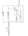
- FIG. 1 is a block diagram showing an outline of the configuration of the signal processing apparatus 100a.
- the signal processing apparatus 100a includes a block boundary detection unit (block boundary detection means, block boundary detection circuit) 11a, a low-pass filter (high frequency component removal means, high frequency component removal circuit) 20, a synchronization processing unit. (Synchronizing means, synchronizing circuit) 30 and signal switching unit (signal switching means, signal switching circuit) 40 are provided.
- the decoding apparatus 200 shown in FIG. It is a decoder that performs a decoding process on an encoded signal encoded in block units by an encoding technique such as H.264.
- the decoding device 200 outputs a decoded signal Sin obtained by decoding the encoded signal.
- the block boundary detection unit 11a detects a block boundary included in the image represented by the decoded signal Sin. Then, the block boundary detection unit 11a outputs a signal indicating the position of the block boundary included in the decoded signal Sin to the signal switching unit 40 as a block boundary detection result.
- the configuration of the block boundary detection unit 11a will be described later.
- a signal output from the block boundary detection unit 11a is referred to as a detection signal S111.
- the low-pass filter 20 is a generally known low-pass filter that removes high-frequency components from the decoded signal Sin. It may be a filter with adjustable frequency characteristics (adaptive). Note that a signal output from the low-pass filter 20 is denoted as a high-frequency removal signal S20.
- the synchronization processing unit 30 includes a delay element inside, and delays the decoded signal Sin in order to synchronize the decoded signal Sin and the high frequency elimination signal S20. Specifically, the decoded signal Sin is delayed by the same delay time as the delay time when the decoded signal Sin passes through the low-pass filter 20. A signal output from the synchronization processing unit 30 is referred to as a synchronization signal S30.
- the signal switching unit 40 is a switch for switching the connection between the connection point In1 and the connection point In2 and the connection point Out according to the detection result of the block boundary by the block boundary detection unit 11a. Specifically, when a block boundary is detected (that is, when the position of the block boundary is indicated by the detection signal S111 output from the block boundary detection unit 11a), one or more positioned near the block boundary For the pixel (hereinafter referred to as the neighboring pixel NP), the connection point In1 and the connection point Out are connected. On the other hand, for a pixel that does not belong to the neighboring pixel NP, the connection point In2 and the connection point Out are connected.
- the pixels belonging to the neighboring pixel NP are predetermined in this embodiment.
- 2L pixels including L consecutive pixels (L is an arbitrary integer greater than or equal to 0) immediately before the block boundary and L consecutive pixels immediately after the block boundary are represented as neighboring pixels NP.
- L is an arbitrary integer greater than or equal to 0
- L consecutive pixels immediately after the block boundary
- two pixels composed of pixels immediately before and after the block boundary are neighboring pixels NP.
- the signal processing device 100a outputs the high-frequency removal signal S20 as the output signal Sout for the neighboring pixels NP located in the vicinity of the block boundary in the decoded signal Sin.
- the synchronization signal S30 is output as the output signal Sout for pixels that do not belong to the neighboring pixel NP.
- the signal processing device 100a causes the DC level to change gently between the blocks before and after the block boundary.
- the block boundary can be made difficult to be recognized by human vision, so that block distortion included in the image represented by the decoded signal Sin can be reduced.
- the detection signal S111 plays a role as an activation signal of a so-called adaptive filter that performs a filtering process that removes a high-frequency component from only a signal near the block boundary.
- FIG. 3 is a block diagram illustrating a configuration of the block boundary detection unit 11a.
- the block boundary detection unit 11a includes a high-pass filter (low frequency component removal unit) 12, a delay processing unit (delay unit) 13, a multiplication unit (multiplication unit) 14, and a detection signal generation unit ( Detection signal generation means) 15 is provided.
- the high-pass filter 12 is a generally known high-pass filter and removes a low-frequency component from the decoded signal Sin. It may be a filter with adjustable frequency characteristics (adaptive). A signal output from the high-pass filter 12 is referred to as a low frequency removal signal S12.
- the delay processing unit 13 outputs a signal obtained by delaying the low frequency removal signal S12 by a time obtained by multiplying N times the block length by a unit time (N is an arbitrary positive integer).
- N is an arbitrary positive integer.
- the delay processing unit 13 includes B ⁇ N delay circuits connected in cascade. Each delay circuit outputs a signal obtained by delaying the input signal by unit time. Note that a signal output from the delay processing unit 13 is referred to as a delay signal S13.
- the delay processing unit 13 delays the low frequency removal signal S12 by unit time ⁇ 8N and outputs it as the delay signal S13.
- H.M. In H.264, since encoding is performed in units of blocks of 4 pixels ⁇ 4 lines (pixels), the block boundary in the image represented by the decoded signal is every 4 pixels in the horizontal direction and every 4 lines (pixels) in the vertical direction. Appear.
- the block length B is “4”. Therefore, in this case, the delay processing unit 13 delays the low frequency removal signal S12 by unit time ⁇ 4N and outputs it as the delay signal S13.
- the horizontal direction is used to reduce block distortion that appears in the horizontal direction.
- the block distortion appearing in the vertical direction is reduced, the block length in the vertical direction is used.
- the multiplication unit 14 generates a multiplication signal S14 by multiplying the low frequency removal signal S12 and the delay signal S13. That is, if the data sequence that constitutes the low frequency removal signal S12 is U1, U2, U3,..., And the data sequence that constitutes the delay signal S13 is V1, V2, V3,. Is a digital signal composed of data strings U1 ⁇ V1, U2 ⁇ V2, U3 ⁇ V3,.
- the low frequency removal signal S12 has a block boundary for each block length, and similarly, the delayed signal S13 also has a block boundary for each block length.
- the low frequency removal signal S12 and the delay signal S13 have a time difference of N times the block length. Therefore, in the multiplication signal S14, the signal value in the vicinity of the block boundary becomes a significantly large value.
- the detection signal generation unit 15 generates a detection signal S111 from the multiplication signal S14 by setting a value whose absolute value is equal to or less than a predetermined threshold to “0”.
- a position having a signal value other than “0” in the detection signal S111 can be regarded as an appearance position of a block boundary included in the image represented by the decoded signal Sin.
- the predetermined threshold value has a configuration that can be appropriately set according to an image represented by a decoded signal.
- FIG. 4 is a schematic diagram illustrating an example of a waveform of a signal handled by each unit of the block boundary detection unit 11a. Note that the waveform of each signal in FIG. 4 is merely a schematic overview, and there are actually a large number of signals with minute values. Particularly in FIGS. 4B to 4E, the position and size of the signal value are represented by the position and length of the line segment for easy understanding.
- FIG. 4A is a schematic diagram showing an example of the waveform of the decoded signal Sin.
- the position of the broken line shown to (a) of FIG. 4 shall be a block boundary.
- FIG. 4 is a schematic diagram showing an example of a waveform of a low frequency removal signal S12 obtained by removing low frequency components from the decoded signal Sin shown in (a) of FIG.
- the waveform shown in FIG. 4B includes an edge component included in the image in addition to the block boundary. Note that the position indicated by the arrow is the position of the block boundary.
- FIG. 4C shows an example of a waveform of a delay signal S13 obtained by delaying the low frequency removal signal S12 shown in FIG. 4B by a time obtained by multiplying the unit time by the length of the block. It is a schematic diagram. As shown in (c) of FIG. 4, the position where the block boundary appears is the same position as the waveform shown in (b) of FIG. Note that the position indicated by the arrow is the position of the block boundary.
- FIG. 4 is a schematic diagram illustrating an example of a waveform of a multiplication signal S14 obtained by multiplying the low frequency removal signal S12 illustrated in (b) of FIG. 4 and the delay signal S13 illustrated in (c) of FIG. FIG.
- the signal value corresponding to the block boundary stands out compared to other signal values. Note that the position indicated by the arrow is the position of the block boundary.
- the signal value not corresponding to the block boundary has no correlation between the low frequency removal signal S12 shown in FIG. 4B and the delayed signal S13 shown in FIG.
- the multiplication signal S14 shown in d) has no value or a small value.
- FIG. 4 is a schematic diagram showing an example of a waveform of the detection signal S111 in which the absolute value is “0” from the multiplication signal S14 shown in (d) of FIG. is there.
- a position where a signal value exists is regarded as a block boundary appearance position.
- FIG. 5 is a block diagram illustrating a configuration of a block boundary detection unit 11a ′ which is a modification of the block boundary detection unit 11a.
- the block boundary detection unit 11a ′ includes an absolute value processing unit 17 that obtains the absolute value of the signal value of the low-frequency removal signal S12 at the subsequent stage of the high-pass filter 12.
- a signal output from the absolute value processing unit 17 is referred to as an absolute value signal S17.
- a signal output from the block boundary detection unit 11a ′ is represented as a detection signal S111 ′.
- FIG. 6 is a block diagram showing a configuration of a block boundary detection unit 11a ′′ which is another modification of the block boundary detection unit 11a.
- the block boundary detection unit 11 a ′′ includes an absolute value processing unit 17 that obtains an absolute value of the signal value of the multiplication signal S 14 after the multiplication unit 14.
- a signal output from the block boundary detection unit 11a ′′ is referred to as a detection signal S111 ′′.
- FIG. 7 is a schematic diagram illustrating an example of a waveform of a signal handled by each unit of the block boundary detection unit 11a ′.
- the waveform of each signal in FIG. 7 is merely a schematic view, and there are actually a large number of signals with minute values.
- the position and size of the signal value are expressed by the position and length of the line segment for easy understanding.
- FIG. 7A is a schematic diagram showing an example of the waveform of the decoded signal Sin. It is the same waveform as the decoded signal Sin shown in FIG.
- (b) of FIG. 7 shows an absolute value signal obtained as a result of obtaining the absolute value of the signal value of the low frequency removal signal S12 obtained by removing the low frequency component from the decoded signal Sin shown in (a) of FIG. It is a schematic diagram which shows an example of the waveform of S17.
- the waveform shown in (b) of FIG. 7 includes many edge components included in the image in addition to the block boundary. Note that the position indicated by the arrow is the position of the block boundary.
- FIG. 7 is a schematic diagram showing an example of a waveform of a delay signal S13 obtained by delaying the absolute value signal S17 shown in (b) of FIG. 7 by a time obtained by multiplying the unit time by the block length.
- FIG. As shown in (c) of FIG. 7, the position where the block boundary appears is the same position as the waveform shown in (b) of FIG. Note that the position indicated by the arrow is the position of the block boundary.
- FIG. 7 is a schematic diagram showing an example of a waveform of a multiplication signal S14 obtained by multiplying the absolute value signal S17 shown in (b) of FIG. 7 and the delay signal S13 shown in (c) of FIG. It is.
- the signal value corresponding to the block boundary stands out compared with other signal values. Note that the position indicated by the arrow is the position of the block boundary.
- the signal value not corresponding to the block boundary has no correlation between the absolute value signal S17 shown in FIG. 7B and the delayed signal S13 shown in FIG.
- FIG. 7 is a schematic diagram showing an example of a waveform of the detection signal S111 ′ in which the absolute value is “0” from the multiplication signal S14 shown in (d) of FIG. It is.
- a position where a signal value exists is regarded as a block boundary appearance position.
- the signal processing device 100 is referred to as a signal processing device 100b.
- members having the same functions as those shown in the first embodiment are denoted by the same reference numerals, and the description thereof is omitted unless specifically described.
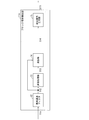
- FIG. 8 is a block diagram showing an outline of the configuration of the signal processing device 100b.
- the signal processing device 100b has a configuration in which the block boundary detection unit 11a is replaced with a block boundary detection unit (block boundary detection means, block boundary detection circuit) 11b in the configuration of the signal processing device 100a. is there.
- a signal output from the block boundary detection unit 11b is referred to as a detection signal S112.
- FIG. 9 is a block diagram illustrating a configuration of the block boundary detection unit 11b.
- the block boundary detection unit 11 b includes a high-pass filter 12, k cascaded delay circuits 18 (k is an arbitrary positive integer), a convolution operation unit (convolution operation means) 19. , And a detection signal generation unit 15.
- Each of the k delay circuits 18 outputs a signal obtained by delaying the input signal by a unit time.
- the value of k is not particularly limited, but the maximum value is the screen resolution (for example, in the case of HDTV, vertical direction: 1080, horizontal direction: 1920), but from the viewpoint of circuit scale and cost. It is desirable that “20” be greater than the block length for which motion correction is performed.
- the convolution operation unit 19 receives the low-frequency removal signal S12 and the signals output from each of the k delay circuits 18, and obtains a convolution sum. Then, the result of the convolution sum is output as a convolution signal S19.
- the convolution operation unit 19 has a “block length B ⁇ 2 centered on a signal to be processed (hereinafter, referred to as a signal of interest) in a signal sequence including k signals to be input. ⁇ 1 ”signals and“ block length B ⁇ 2-1 ”signals centered on a signal separated from the signal of interest by a block length B, by calculating a generally known convolution sum, A convolution signal S19 corresponding to the signal is output.
- the convolution operation unit 19 outputs a convolution signal S19 corresponding to the new signal of interest by obtaining the same convolution sum as described above for the new signal of interest. And the convolution operation part 19 repeats the said process.
- the convolution unit 19 obtains a convolution sum represented by the following formula (1), for example.
- f (n) indicates the signal value of the signal n.
- required by following Numerical formula (1) is shown in FIG.
- Equation (2) is an equation for calculating the correlation between a plurality of adjacent pixels.
- the detection signal generation unit 15 of the present embodiment generates the detection signal S112 from the convolution signal S19 by setting a value whose absolute value is equal to or less than a predetermined threshold to “0”. As a result, a position having a signal value other than “0” in the detection signal S112 is regarded as an appearance position of a block boundary included in the image represented by the decoded signal Sin.
- the block boundary detection unit 11b includes the “block length B ⁇ 2-1” signals centered on the target signal to be processed in the low frequency removal signal S12 and the block length B from the target signal.
- a convolution sum is obtained from “block length B ⁇ 2-1” signals centered on signals separated by a distance.
- the block boundary detection unit 11b determines the block length B from the signal group composed of continuous “block length B ⁇ 2-1” signals in the low frequency removal signal S12 and the signal located at the center of the signal group.
- a convolution sum is obtained from a signal group consisting of continuous “block length B ⁇ 2-1” signals centered on signals separated by a distance.
- the signal processing device 100b can also detect block boundaries that are difficult to detect with the signal processing device 100a.
- the signal processing device 100b when calculating the convolution sum, since the calculation is performed using many signal values, the signal processing device 100b requires more processing time than the signal processing device 100a and is not suitable for real-time processing. Therefore, the signal processing device 100b is suitable when the image represented by the decoded signal Sin is a still image.
- FIG. 11 is a schematic diagram illustrating a state in which the block boundary detection unit 11a and the block boundary detection unit 11b perform operations on the signal sequence included in the low frequency removal signal S12. D1 to d13 shown in FIG. 11 are labels attached to identify each signal, and the numerical values attached in parentheses are signal values.
- the block boundary detection unit 11a performs a calculation of d5 ⁇ d9, for example, as a calculation C1 illustrated in FIG. The result of this calculation is “90”.
- the multiplication signal S14 generated by the block boundary detection unit 11a and the convolution signal S19 generated by the block boundary detection unit 11b will be described.
- the low frequency removal signal S12 shown in FIG. 12 is an excerpt of the low frequency removal signal S12 shown in FIG.
- the block boundary detection unit 11a is described with reference to FIG. Then, an operation of d5 ⁇ d9 is performed on d5, similarly, an operation of d6 ⁇ d10 is performed on d6, and an operation of d7 ⁇ d11 is performed on d7.
- a multiplication signal S14 shown in FIG. 12 is generated.
- the frequency characteristic of the low-pass filter 20 is not changed.
- the frequency characteristic of the low-pass filter 20 may be adjusted according to the magnitude of block distortion. Specifically, the frequency characteristics may be adjusted so that the amount of high-frequency components remaining in the high-frequency removal signal S20 decreases as the block distortion increases. Thereby, the greater the block distortion, the higher the degree of block distortion reduction.
- each block of the signal processing device 100 is realized by software using a CPU (central processing unit), it is possible to easily adjust the frequency characteristics of the low-pass filter 20.
- the magnitude of block distortion is the average pixel value (DC level) in the block immediately before the block boundary where the block distortion occurs and the average pixel value (DC level) in the block immediately after the block boundary. It shall be measured by the magnitude of the difference (hereinafter referred to as DC level difference).
- the signal processing device 100 is referred to as a signal processing device 100c.
- a signal processing device 100c members having the same functions as those of the members shown in the first and second embodiments are given the same reference numerals, and explanations thereof are omitted unless otherwise specified.
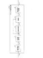
- FIG. 13 is a block diagram showing an outline of the configuration of the signal processing device 100c.
- the signal processing apparatus 100c includes a block boundary detection unit 11, a low-pass filter 20, a synchronization processing unit 30, a signal switching unit 40, and a DC level difference calculation unit (DC level difference calculation unit) 51.
- the low-pass filter 20 of this embodiment shall be a filter which can adjust a frequency characteristic (adaptive).
- the block boundary detection unit 11 is either the block boundary detection unit 11a or the block boundary detection unit 11b.
- a signal output from the block boundary detection unit 11 is referred to as a detection signal S11.
- the detection signal S11 is the detection signal S111.
- the detection signal S11 is the detection signal S112.
- the DC level difference calculation unit 51 performs direct current of the block immediately before the block boundary.
- a DC level difference that is a difference between the level and the DC level of the block immediately after the block boundary is calculated.
- the filter coefficient of the low-pass filter 20 is adjusted according to the calculated DC level difference. Specifically, the filter coefficient of the low-pass filter 20 is set so that the amount of high-frequency components removed from the decoded signal Sin increases as the DC level difference increases. As a result, the degree of removing the high frequency component from the decoded signal Sin can be increased.
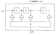
- the frequency characteristics are adjusted by setting the values of the filter coefficients ⁇ 0 to ⁇ n shown in FIG. Some filter coefficients may be set to “0”.
- the timing for switching the connection between the connection point In1 and the connection point In2 and the connection point Out in the signal switching unit 40 does not vary for each block boundary.
- the greater the block distortion the longer the period during which the signal switching unit 40 connects the connection point In1 and the connection point Out near the block boundary.
- the greater the block distortion the longer the period during which the high-frequency removal signal S20 is output as the output signal Sout in the vicinity of the block boundary. Therefore, the degree of reduction in block distortion can be increased.
- the magnitude of block distortion is measured by the magnitude of the DC level difference between the DC level of the block immediately before the block boundary where the block distortion occurs and the DC level of the block immediately after the block boundary.
- the signal processing apparatus 100 is referred to as a signal processing apparatus 100d.
- members having the same functions as those shown in the first to third embodiments are given the same reference numerals, and explanations thereof are omitted unless otherwise specified.
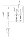
- FIG. 15 is a block diagram showing an outline of the configuration of the signal processing device 100d.
- the signal processing device 100d includes a block boundary detection unit 11, a low-pass filter 20, a synchronization processing unit 30, a signal switching unit 41, and a DC level difference calculation unit (DC level difference calculation unit) 52. I have.
- the DC level difference calculation unit 52 performs direct current of the block immediately before the block boundary. A DC level difference that is a difference between the level and the DC level of the block immediately after the block boundary is calculated. Then, the calculated DC level difference is output to the signal switching unit 41.
- the signal switching unit 41 determines the connection point In1, the connection point In2, and the connection point Out according to the detection result of the block boundary by the block boundary detection unit 11 and the DC level difference calculated by the DC level difference calculation unit 52. This is a switch for switching the connection.
- the signal switching unit 41 is positioned in the vicinity of the block boundary when the block boundary is detected by the block boundary detection unit 11 (that is, when the position of the block boundary is indicated by the detection signal S11).
- the connection point In1 and the connection point Out are connected.
- the connection point In2 and the connection point Out are connected.
- the signal switching unit 41 determines pixels belonging to the neighboring pixel NP according to the DC level difference calculated by the DC level difference calculating unit 52. Specifically, the adjustment is performed such that the larger the DC level difference is, the more pixels belonging to the neighboring pixel NP are increased. As a result, the larger the DC level difference, the larger the number of signals that are the targets for removing high-frequency components from the decoded signal Sin.
- the neighboring pixel NP is 2N pixels including N consecutive pixels (N is an arbitrary integer greater than or equal to 0) immediately before the block boundary and N consecutive pixels immediately after the block boundary. In this case, adjustment is performed so that the value of N increases as the DC level difference increases. As a specific example, when the DC level difference is 16, the value of N is “3”, and when the DC level difference is 8 or less, the value of N is “2”.
- the signal processing device 100 that reduces horizontal block distortion is referred to as a signal processing device 100A.
- the delay elements included in the respective units of the signal processing apparatus 100 may be those that delay the input signal in the horizontal direction (delay in units of pixels).
- the block boundary detection unit 11 is a signal representing a pixel group composed of pixels arranged adjacent to each other in the horizontal direction of the image represented by the decoded signal Sin (hereinafter referred to as a horizontal direction signal).
- the low-pass filter 20 generates a high-frequency removal signal S20 by removing high-frequency components from the horizontal signal.
- the synchronization processing unit 30 generates a synchronization signal S30 that is synchronized with the high-frequency removal signal S20 by delaying the horizontal direction signal. Then, the signal switching unit 40 performs processing using a pixel located in the vicinity of the block boundary detected by the block boundary detection unit 11 in the horizontal direction as a neighboring pixel NP.
- the signal processing device 100 that reduces block distortion in the vertical direction is referred to as a signal processing device 100B.
- the delay element included in each unit of the signal processing apparatus 100 may be any element that delays the input signal in the vertical direction (that delays in units of lines).
- the block boundary detection unit 11 is a signal representing a pixel group composed of pixels lined up adjacent in the vertical direction of the image represented by the decoded signal Sin (hereinafter referred to as a vertical direction signal).
- the low-pass filter 20 generates a high-frequency removal signal S20 by removing a high-frequency component from the vertical direction signal.
- the synchronization processing unit 30 generates a synchronization signal S30 that is synchronized with the high frequency removal signal S20 by delaying the vertical direction signal. Then, the signal switching unit 40 performs processing using a pixel located in the vicinity of the block boundary detected by the block boundary detection unit 11 in the vertical direction as a neighboring pixel NP.
- connection configuration of the signal processing device 100A and the signal processing device 100B is as shown in FIG. As shown in FIG. 16A, the decoded signal Sin is input to the signal processing device 100A, and the output signal from the signal processing device 100A is input to the signal processing device 100B. Thereby, in the image represented by the output signal from the signal processing device 100B, both horizontal block distortion and vertical block distortion are reduced.
- connection order of the signal processing device 100A and the signal processing device 100B may be reversed. That is, as shown in FIG. 16B, the decoded signal Sin may be input to the signal processing device 100B, and the output signal from the signal processing device 100B may be connected to the signal processing device 100A.
- FIG. 17 is a diagram illustrating an example of an image represented by the decoded signal Sin. Such images are often seen in images obtained from websites. As shown in FIG. 17, block distortion is prominently seen in flowers, flower pots, outer walls of buildings, and the like.
- FIG. 18 is a diagram illustrating an example of an image after block distortion is reduced by the signal processing device 100 with respect to the image illustrated in FIG. In the image shown in FIG. 18, it can be seen that the block distortion included in the image in FIG. 17 is reduced.
- each block of the signal processing apparatus 100 may be configured as hardware by a logic circuit formed on an integrated circuit (IC chip), or software using a CPU (central processing unit) as follows. It may be realized by.
- IC chip integrated circuit
- CPU central processing unit
- the signal processing apparatus 100 When implemented by software, the signal processing apparatus 100 includes a CPU that executes instructions of a control program for realizing each function, a ROM (read only memory) that stores the program, and a RAM (random access memory) that develops the program. And a storage device (recording medium) such as a memory for storing the program and various data.
- An object of the present invention is a recording medium on which a program code (execution format program, intermediate code program, source program) of a control program of the signal processing apparatus 100, which is software that realizes the functions described above, is recorded so as to be readable by a computer. This can also be achieved by supplying the signal processing apparatus 100 and reading and executing the program code recorded on the recording medium by the computer (or CPU or MPU).
- Examples of the recording medium include tapes such as magnetic tapes and cassette tapes, magnetic disks such as floppy (registered trademark) disks / hard disks, and disks including optical disks such as CD-ROM / MO / MD / DVD / CD-R.
- IC cards including memory cards
- semiconductor memories such as mask ROM / EPROM / EEPROM / flash ROM
- logic circuits such as PLD (Programmable logic device), etc. it can.
- the signal processing apparatus 100 may be configured to be connectable to a communication network, and the program code may be supplied via the communication network.
- the communication network is not particularly limited.
- the Internet intranet, extranet, LAN, ISDN, VAN, CATV communication network, virtual private network, telephone line network, mobile communication network, satellite communication. A net or the like is available.
- the transmission medium constituting the communication network is not particularly limited.
- infrared rays such as IrDA and remote control
- Bluetooth It can also be used for wireless such as registered trademark), IEEE 802.11 wireless, HDR (High Data Rate), NFC (Near Field Communication), DLNA (Digital Living Network Alliance), mobile phone network, satellite line, terrestrial digital network, etc. .
- means does not necessarily mean physical means, but includes cases where the functions of each means are realized by software. Further, the function of one means may be realized by two or more physical means, or the functions of two or more means may be realized by one physical means.
- the signal processing apparatus receives a decoded signal obtained by decoding a coded signal obtained by coding a signal representing an image in units of blocks, and inputs the image represented by the decoded signal.
- a signal processing apparatus that outputs an output signal representing an image with reduced block distortion generated at the boundary between adjacent blocks in the block, and that detects a boundary between adjacent blocks in the image represented by the decoded signal
- a high-frequency component removing unit that generates a high-frequency removed signal by removing a high-frequency component from the decoded signal
- a synchronizing unit that generates a synchronizing signal that is synchronized with the high-frequency removed signal by delaying the decoded signal;
- an integrated circuit receives a decoded signal obtained by decoding a coded signal obtained by coding a signal representing an image in units of blocks, and an adjacent block in the image represented by the decoded signal
- An integrated circuit that outputs an output signal representing an image with reduced block distortion generated at the boundary of the block, the block boundary detection circuit detecting a boundary between adjacent blocks in the image represented by the decoded signal, and the decoding
- a high-frequency component removal circuit that generates a high-frequency removal signal by removing high-frequency components from the signal; a synchronization circuit that generates a synchronization signal synchronized with the high-frequency removal signal by delaying the decoded signal; and the block boundary detection
- the high frequency component is removed from only the signal near the block boundary in the decoded signal, and the result is output as an output signal.
- the block boundary detection unit further includes a low frequency component removal unit that generates a low frequency removal signal by removing a low frequency component from the decoded signal, and the low frequency component.
- Multiplication that generates a multiplication signal by multiplying the low-frequency removal signal and the delay signal by delay means that generates a delay signal obtained by delaying the cancellation signal by a time obtained by multiplying the unit time by the length of the block.
- the configuration may be such that the boundary is detected.
- a low-frequency removal signal is generated by removing low-frequency components from the decoded signal.
- a delay signal is generated by delaying the low frequency removal signal by a time obtained by multiplying the unit time by the length of the block.
- a multiplication signal is generated by multiplying the low frequency removal signal and the delay signal.
- a detection signal is generated by setting a signal value whose absolute value is equal to or less than a predetermined threshold among the multiplication signals to 0. Then, the position of a signal whose signal value is not 0 is detected as a block boundary in the detection signal.
- the block boundary detection unit further includes a low frequency component removing unit that generates a low frequency removal signal by removing a low frequency component from the decoded signal, and the low frequency component.
- a signal group consisting of a number of consecutive signals that is one less than twice the block length and a signal that is separated from the signal located in the center of the signal group by the length of the block.
- a convolution operation means for outputting a convolution signal by obtaining a convolution sum from a signal group consisting of a number of consecutive signals one less than twice the length; and a signal value having an absolute value of a predetermined threshold value or less among the convolution signals.
- Detection signal generating means for generating a detection signal by setting 0 to 0, and detecting the position of a signal whose signal value is not 0 in the detection signal as the boundary It may be a configuration that.
- a low frequency removal signal is generated by removing low frequency components from the decoded signal. Then, in the low frequency elimination signal, a signal group composed of a number of consecutive signals less than twice the block length, and a signal separated from the signal located at the center of the signal group by the length of the block, as a center. Then, a convolution signal is output by obtaining a convolution sum from a signal group consisting of a number of consecutive signals that is one less than twice the block length. Then, a detection signal is generated by setting a signal value whose absolute value is equal to or less than a predetermined threshold among the convolution signals to 0. Then, the position of a signal whose signal value is not 0 is detected as a block boundary in the detection signal.
- the boundary of the block can be detected appropriately with a simple configuration, and the signal value of the detection signal increases because the convolution sum is obtained. There is an effect of obtaining.
- the high-frequency component removing unit is a low-pass filter, and when the boundary is detected by the block boundary detecting unit, a block immediately before the detected boundary is detected.
- a DC level difference calculating means for calculating a difference between the DC level of the block and the DC level of the block immediately after the detected boundary, and setting the frequency characteristic of the filter according to the calculated difference.
- the frequency characteristics of the filter are further set according to the magnitude of the difference between the DC level of the block immediately before the block boundary and the DC level of the immediately following block.
- the filter coefficient is set so that the higher the difference, the greater the amount of high frequency components removed from the decoded signal.
- the signal processing apparatus when the boundary is detected by the block boundary detecting means, the signal processing apparatus according to the present invention is configured such that the direct current level of the block immediately before the detected boundary and the direct current of the block immediately after the detected boundary are detected.
- DC level difference calculating means for calculating a difference from the level is further provided, and the signal switching means is configured to set the neighboring pixels according to the magnitude of the difference calculated by the DC level difference calculating means. Also good.
- the neighboring pixels are further set according to the magnitude of the difference between the DC level of the block immediately before the block boundary and the DC level of the immediately following block. For example, the larger the difference is, the more pixels are included in the neighboring pixels.
- the larger the difference the greater the number of signals that are the targets for removing high-frequency components from the decoded signal.
- the block boundary detecting means detects the boundary from a horizontal direction signal representing a pixel group consisting of pixels arranged adjacent to each other in the horizontal direction of the image represented by the decoded signal.
- the high-frequency component removal means generates the high-frequency removal signal by removing a high-frequency component from the horizontal signal, and the synchronization means delays the horizontal signal to
- the synchronization signal is generated in synchronization with a high-frequency rejection signal, and the signal switching unit is configured such that a pixel located in the horizontal vicinity of the boundary detected by the block boundary detection unit is set as the neighboring pixel. Also good.
- the block boundary detecting means detects the boundary from a vertical direction signal representing a pixel group composed of pixels arranged adjacent to each other in the vertical direction of the image represented by the input signal.
- the high-frequency component removal means generates the high-frequency removal signal by removing a high-frequency component from the vertical direction signal, and the synchronization means delays the vertical direction signal and outputs the high-frequency removal signal.
- the synchronization signal that is synchronized with the high-frequency rejection signal is generated, and the signal switching unit has a configuration in which a pixel located in the vicinity of the boundary in the vertical direction detected by the block boundary detection unit is the neighborhood pixel. Also good.
- the signal processing device may be realized by a computer.
- a control program for the signal processing device that causes the signal processing device to be realized by the computer by causing the computer to operate as each of the means, and A computer-readable recording medium on which it is recorded also falls within the scope of the present invention.
- a chip including the above integrated circuit, a ROM (read only memory) storing a control program, and the like fall within the scope of the present invention.
- the present invention can be applied to an apparatus for processing an image signal.
- the present invention can be suitably applied to a display device that displays a still image or a moving image.
- Block boundary detection unit (block boundary detection means, block boundary detection circuit) 12 High-pass filter (low frequency component removal means) 13 Delay processing unit (delay means) 14 Multiplier (Multiplier) 15 Detection signal generator (detection signal generator) 19 Convolution operation part (convolution operation means) 20 Low-pass filter (high-frequency component removal means, high-frequency component removal circuit) 30 Synchronization processing unit (synchronization means, synchronization circuit) 40 Signal switching part (signal switching means, signal switching circuit) 51, 52 DC level difference calculation unit (DC level difference calculation means) 100, 100a to 100d Signal processing device (integrated circuit) 100A, 100B Signal processing device (integrated circuit) Sin decoded signal Sout output signal S11, S111, S112 detection signal S12 low frequency removal signal S13 delay signal S14 multiplication signal S19 convolution signal S20 high frequency removal signal S30 synchronization signal NP neighboring pixels
Landscapes
- Engineering & Computer Science (AREA)
- Multimedia (AREA)
- Signal Processing (AREA)
- Physics & Mathematics (AREA)
- General Physics & Mathematics (AREA)
- Theoretical Computer Science (AREA)
- Compression Or Coding Systems Of Tv Signals (AREA)
Abstract
信号処理装置(100a)は、画像を表す信号をブロック単位で符号化した符号化信号を復号して得られる復号化信号(Sin)で表される画像における隣接するブロックの境界を検出するブロック境界検出部(11a)と、復号化信号(Sin)から高周波成分を除去することによって高周波除去信号(S20)を生成する低域通過フィルタ(20)と、復号化信号(Sin)を遅延させることにより高周波除去信号(S20)と同期する同期信号(S30)を生成する同期処理部(30)と、上記境界が検出されたとき、該検出された境界の近傍に位置する1または複数の画素である近傍画素については、高周波除去信号(S20)を出力するとともに、近傍画素ではない画素については、同期信号(S30)を出力する信号切替部(40)とを備える。
Description
本発明は、画像に含まれるブロックの境界で生じるブロック歪みを低減する信号処理装置等に関するものである。
近年、LSI(large-scale integration)技術の進歩により、画像のデジタル符号化が行なわれるようになった。デジタル符号化を行なうことにより、画像を1/10から1/200程度のデータ量に圧縮することができるため、DVD(digital video disc)等の記録媒体への格納や、デジタル放送およびインターネット配信等が実現可能となっている。
一方、画像を圧縮しすぎると、ブロック歪み(ブロックノイズ)と称される画質劣化が生じることが知られている。例えば、JPEG(Joint Photographic Experts Group)、MPEG(Moving Picture Experts Group)-2、H.264などの符号化方式で画像を圧縮すると、矩形のブロック歪みが生じることが知られている。そのため、ブロック歪みを低減するために、従来から様々な技術が提案されている。
画像の符号化において、ブロックの境界は各フレームで固定されており、ブロックの境界は符号化されたストリームの情報を解析することによって容易に知り得ることができる。そのため、MPEG-4 Part10(H.264)では、いわゆるデブロッキングフィルタを用いてブロック歪みを低減することが定められている。デブロッキングフィルタには様々なものが提案されているが、いずれも、符号化されたストリームから得られるブロックの境界の位置情報を用いるものである。
デブロッキングフィルタを用いてブロック歪みを低減する技術として、特許文献1には、動き推定処理が施されたフレームにおける可変サイズの動き推定ブロックを取得し、取得された動き推定ブロックに従って、前記フレームに対してデブロックフィルタ処理を施す技術が開示されている。
また、ブロック歪みを低減する技術として、特許文献2には、1フレームの画面内の局所的な箇所で発生するようなブロック歪みに対応するブロック歪み低減装置が開示されている。さらに、特許文献3には、強度が異なる複数のフィルタを切り替えることにより、視覚的な影響を抑えたフィルタリングを行なうブロック歪み低減装置が開示されている。
しかしながら、特許文献1に開示されているような、デブロッキングフィルタを用いてブロック歪みを低減させる技術では、符号化されたストリームからブロックの境界の位置を得るため、当該技術は、復号が完了している画像に対しては適用することはできない。つまり、Webサイトから入手可能な画像などの、復号が完了している画像に対しては、適用することはできない。
また、特許文献1~3には、ブロックの境目を検出する具体的な方法は示されていない。特許文献1~3では、ブロックの境目が検出されているものとして、ブロックの境目にフィルタをかけてブロック歪みを見えにくくする手法を示しているだけである。つまり、ブロックの境界の位置が分からないとき(例えば、復号が完了している画像)には、特許文献1~3に開示されている技術は適用することができない。
本発明は、上記の問題点に鑑みてなされたものであり、その目的は、画像に含まれるブロックの境界を示す情報が入力されなくても、ブロックの境界を検出してブロック歪みを低減することができる信号処理装置等を提供することにある。
上記課題を解決するために、本発明に係る信号処理装置は、画像を表す信号をブロック単位で符号化した符号化信号を復号して得られる復号化信号を入力とし、上記復号化信号で表される画像における隣接するブロックの境界で生じるブロック歪みを低減した画像を表す出力信号を出力する信号処理装置であって、上記復号化信号で表される画像における隣接するブロックの境界を検出するブロック境界検出手段と、上記復号化信号から高周波成分を除去することによって高周波除去信号を生成する高周波成分除去手段と、上記復号化信号を遅延させることにより上記高周波除去信号と同期する同期信号を生成する同期手段と、上記ブロック境界検出手段によって上記境界が検出されたとき、該検出された境界の近傍に位置する1または複数の画素である近傍画素については、上記高周波除去信号を上記出力信号として出力するとともに、上記近傍画素ではない画素については、上記同期信号を上記出力信号として出力する信号切替手段とを備えることを特徴としている。
また、本発明に係る集積回路は、画像を表す信号をブロック単位で符号化した符号化信号を復号して得られる復号化信号を入力とし、上記復号化信号で表される画像における隣接するブロックの境界で生じるブロック歪みを低減した画像を表す出力信号を出力する集積回路であって、上記復号化信号で表される画像における隣接するブロックの境界を検出するブロック境界検出回路と、上記復号化信号から高周波成分を除去することによって高周波除去信号を生成する高周波成分除去回路と、上記復号化信号を遅延させることにより上記高周波除去信号と同期する同期信号を生成する同期回路と、上記ブロック境界検出回路によって上記境界が検出されたとき、該検出された境界の近傍に位置する1または複数の画素である近傍画素については、上記高周波除去信号を上記出力信号として出力するとともに、上記近傍画素ではない画素については、上記同期信号を上記出力信号として出力する信号切替回路とを備えることを特徴としている。
上記の構成によれば、信号処理装置は、復号化信号で表される画像における隣接するブロックの境界を検出する。そして、信号処理装置は、上記境界を検出したとき、該検出した境界の近傍に位置する1または複数の画素である近傍画素については、復号化信号から高周波成分を除去した高周波除去信号を出力信号として出力する。一方、上記近傍画素ではない画素については、復号化信号を遅延させることにより高周波除去信号と同期する同期信号を出力信号として出力する。
よって、復号化信号のうち、ブロックの境界付近の信号のみから高周波成分を除去した上で、出力信号として出力する。これにより、ブロックの境界の前後のブロック間で、ブロック内の平均画素値(直流レベル)が緩やかに変化するようにする。
したがって、ブロックの境界を人間の視覚に認識されにくいものとすることができ、その結果、復号化信号で表される画像に含まれるブロック歪みを低減することができるという効果を奏する。
本発明に係る信号処理装置を、静止画や動画像を表示するディスプレイ装置に組み込んで用いることにより、Webサイトから入手可能な画像等の復号済みの画像を精細感を高めて表示することができる。
また、ある符号化方式で符号化されている画像を別の符号化方式で符号化しなおすケースにおいても有効である。例えば、MPEG-2で符号化されている画像を復号して得られる画像をMPEG-4で再符号化する場合、復号して得られる画像にはブロック歪みが生じ得る。そこで、復号して得られる画像に対してブロック歪みを低減する処理を施すことにより、MPEG-4で再符号化した画像に含まれるブロック歪みを低減することができる。
以上のように、本発明に係る信号処理装置は、画像を表す信号をブロック単位で符号化した符号化信号を復号して得られる復号化信号を入力とし、上記復号化信号で表される画像における隣接するブロックの境界で生じるブロック歪みを低減した画像を表す出力信号を出力する信号処理装置であって、上記復号化信号で表される画像における隣接するブロックの境界を検出するブロック境界検出手段と、上記復号化信号から高周波成分を除去することによって高周波除去信号を生成する高周波成分除去手段と、上記復号化信号を遅延させることにより上記高周波除去信号と同期する同期信号を生成する同期手段と、上記ブロック境界検出手段によって上記境界が検出されたとき、該検出された境界の近傍に位置する1または複数の画素である近傍画素については、上記高周波除去信号を上記出力信号として出力するとともに、上記近傍画素ではない画素については、上記同期信号を上記出力信号として出力する信号切替手段とを備えている。
また、本発明に係る集積回路は、画像を表す信号をブロック単位で符号化した符号化信号を復号して得られる復号化信号を入力とし、上記復号化信号で表される画像における隣接するブロックの境界で生じるブロック歪みを低減した画像を表す出力信号を出力する集積回路であって、上記復号化信号で表される画像における隣接するブロックの境界を検出するブロック境界検出回路と、上記復号化信号から高周波成分を除去することによって高周波除去信号を生成する高周波成分除去回路と、上記復号化信号を遅延させることにより上記高周波除去信号と同期する同期信号を生成する同期回路と、上記ブロック境界検出回路によって上記境界が検出されたとき、該検出された境界の近傍に位置する1または複数の画素である近傍画素については、上記高周波除去信号を上記出力信号として出力するとともに、上記近傍画素ではない画素については、上記同期信号を上記出力信号として出力する信号切替回路とを備えている。
よって、復号化信号のうち、ブロックの境界付近の信号のみから高周波成分を除去した上で、出力信号として出力する。
したがって、ブロックの境界を人間の視覚に認識されにくいものとすることができ、その結果、復号化信号で表される画像に含まれるブロック歪みを低減することができるという効果を奏する。
本発明の他の目的、特徴、および優れた点は、以下に示す記載によって十分分かるであろう。また、本発明の利点は、添付図面を参照した次の説明で明白になるであろう。
(信号処理装置の概要)
各実施形態に係る信号処理装置(集積回路)100は、MPEG-2やH.264などの符号化技術によって符号化された信号を復号して得られる信号に残存するブロック歪みを低減する装置である。具体的には、信号処理装置100は、画像を表す信号をブロック単位で符号化した信号(以下、符号化信号と表記する)を復号して得られる信号(以下、復号化信号と表記する)を入力とし、該入力された復号化信号で表される画像における隣接するブロックの境界の近傍のみから高周波成分を除去することにより、ブロック歪みを低減するものである。
各実施形態に係る信号処理装置(集積回路)100は、MPEG-2やH.264などの符号化技術によって符号化された信号を復号して得られる信号に残存するブロック歪みを低減する装置である。具体的には、信号処理装置100は、画像を表す信号をブロック単位で符号化した信号(以下、符号化信号と表記する)を復号して得られる信号(以下、復号化信号と表記する)を入力とし、該入力された復号化信号で表される画像における隣接するブロックの境界の近傍のみから高周波成分を除去することにより、ブロック歪みを低減するものである。
背景技術の欄にて説明したように、従来から知られているデブロッキングフィルタは、符号化信号に含まれるブロックの境界(以下、ブロック境界と表記する)の位置に関する情報を用いて、ブロック歪みを低減するものである。これに対して、信号処理装置100は、復号化後の復号化信号で表される画像からブロック境界を検出し、該検出したブロック境界に対してブロック歪みを低減する処理を施すものであり、従来から知られているデブロッキングフィルタとは大きく異なる。
図2を参照しながら、信号処理装置100にて施す処理の概略について説明する。図2は、連続するブロック毎にブロック内の平均画素値(直流レベル)を簡略化して示す模式図である。ブロック境界にて直流レベルが変化するほど、ブロック境界が人間の視覚に認識されやすくなる。そこで、信号処理装置100では、ブロック境界の近傍に対して、低域通過型のフィルタ(ローパスフィルタ)によって高周波成分を除去する処理を施す。つまり、図2(a)に示した波形を、図2(b)に示す波形のようにして、ブロック境界の前後にて直流レベルが緩やかに変化するようにする。なお、図2に示すグラフの縦軸は輝度値を示しているが、輝度値に限らず色信号でもよい。また、図2に示すB11、B12、B13のそれぞれはブロック境界の位置であるものとする。
これにより、ブロック境界を人間の視覚に認識されにくいものとすることができる。なお、全ての画素について高周波成分を除去すると画像全体が精細感を失うので、ブロック境界の近傍についてのみ高周波成分を除去している。
このように、信号処理装置100を用いることによって、ブロック境界を人間の視覚に認識されにくいものとすることができるので、ブロック歪みを低減することができる。
例えば、Webサイトから入手可能な画像にはブロック歪みが含まれるものが多いことから、信号処理装置100を用いることによりブロック歪みを低減することができ、精細感を高めた画像を表示することができる。
また、ある符号化方式で符号化されている画像を別の符号化方式で符号化しなおすケースにおいても信号処理装置100は有効である。例えば、MPEG-2で符号化されている画像を復号して得られる画像をMPEG-4で再符号化する場合、復号して得られる画像にはブロック歪みが生じ得る。そこで、復号して得られる画像に対して信号処理装置100にてブロック歪みを低減する処理を施すことにより、MPEG-4で再符号化した画像に含まれるブロック歪みを低減することができる。
信号処理装置100は、静止画や動画像を表示するディスプレイ装置に組み込んで用いることが好適である。特に、画像処理用のLSIやTCON(タイミングコントローラ)などに組み込んで用いることが好適であり、ディスプレイに表示される画像に含まれるブロック歪みを大幅に低減することができる。
なお、以下では、信号処理装置100に入力される復号化信号を、復号化信号Sinと表記する。また、信号処理装置100から出力される信号を、出力信号Soutと表記する。
復号化信号Sinで表される画像は、静止画像であってもよいし、動画像であってもよい。さらに、動画像は、例えば、標準画質テレビジョン(SDTV:Standard Definition Television)または高精細テレビジョン(HDTV:High Definition Television)の受像機等にて、リアルタイムに表示されるものであってもよい。
また、復号化信号Sinは、画像の水平方向(横方向、主走査方向)に隣接して並ぶ画素の画素値から成るデータ列(画素値の系列)によって構成されているものとして説明するが、画像の垂直方向(縦方向、副走査方向)に隣接して並ぶ画素の画素値から成るデータ列によって構成されていてもよい。
なお、後述する信号処理装置100a~100dを区別しないときは、単に「信号処理装置100」と表記する。
〔実施形態1〕
本発明の一実施形態について、図1、および、図3から図7に基づいて説明すると以下の通りである。本実施形態に係る信号処理装置100を、信号処理装置100aと表記する。
本発明の一実施形態について、図1、および、図3から図7に基づいて説明すると以下の通りである。本実施形態に係る信号処理装置100を、信号処理装置100aと表記する。
(信号処理装置の構成の概要)
図1を参照しながら、信号処理装置100aの構成の概要について説明する。図1は、信号処理装置100aの構成の概要を示すブロック図である。同図に示すように、信号処理装置100aは、ブロック境界検出部(ブロック境界検出手段、ブロック境界検出回路)11a、低域通過フィルタ(高周波成分除去手段、高周波成分除去回路)20、同期処理部(同期手段、同期回路)30、および信号切替部(信号切替手段、信号切替回路)40を備えている。
図1を参照しながら、信号処理装置100aの構成の概要について説明する。図1は、信号処理装置100aの構成の概要を示すブロック図である。同図に示すように、信号処理装置100aは、ブロック境界検出部(ブロック境界検出手段、ブロック境界検出回路)11a、低域通過フィルタ(高周波成分除去手段、高周波成分除去回路)20、同期処理部(同期手段、同期回路)30、および信号切替部(信号切替手段、信号切替回路)40を備えている。
なお、同図に示す復号化装置200は、MPEG-2やH.264などの符号化技術によってブロック単位で符号化された符号化信号に対して、復号化処理を施すデコーダである。復号化装置200は、当該符号化信号を復号して得られる復号化信号Sinを出力する。
ブロック境界検出部11aは、復号化信号Sinで表される画像に含まれるブロック境界を検出する。そして、ブロック境界検出部11aは、ブロック境界の検出結果として、復号化信号Sinに含まれるブロック境界の位置を示している信号を信号切替部40に出力する。ブロック境界検出部11aの構成は後述する。なお、ブロック境界検出部11aから出力される信号を、検出信号S111と表記する。
次に、低域通過フィルタ20は、一般に知られているローパスフィルタであり、復号化信号Sinから高周波成分を除去するものである。周波数特性が調整可能な(アダプティブな)フィルタであってもよい。なお、低域通過フィルタ20から出力される信号を、高周波除去信号S20と表記する。
次に、同期処理部30は、内部に遅延素子を含んでおり、復号化信号Sinと高周波除去信号S20とを同期させるために復号化信号Sinを遅延させるものである。具体的には、復号化信号Sinが低域通過フィルタ20を通過する際に遅延する時間と同じ遅延時間だけ復号化信号Sinを遅延させる。同期処理部30から出力される信号を、同期信号S30と表記する。
次に、信号切替部40は、ブロック境界検出部11aによるブロック境界の検出結果に従って、接続点In1および接続点In2と、接続点Outとの接続を切り替えるスイッチである。具体的には、ブロック境界が検出されたとき(つまり、ブロック境界検出部11aから出力される検出信号S111にてブロック境界の位置が示されるとき)、当該ブロック境界の近傍に位置する1または複数の画素(以下、近傍画素NPと表記する)については、接続点In1と接続点Outとを接続する。一方、近傍画素NPに属さない画素については、接続点In2と接続点Outとを接続する。
なお、近傍画素NPに属する画素は、本実施形態では予め定められているものとする。一例としては、ブロック境界の直前の連続するL(Lは0以上の任意の整数)個の画素と、ブロック境界の直後の連続するL個の画素とから成る2L個の画素を、近傍画素NPとする。例えば、Lの値が“1”である場合、ブロック境界の直前および直後の画素から成る2個の画素が、近傍画素NPとなる。
上記構成により、信号処理装置100aは、復号化信号Sinのうち、ブロック境界の近傍に位置する近傍画素NPについては、高周波除去信号S20を出力信号Soutとして出力する。一方、復号化信号Sinのうち、近傍画素NPに属さない画素については、同期信号S30を出力信号Soutとして出力する。
よって、信号処理装置100aは、ブロック境界の前後のブロック間で直流レベルが緩やかに変化するようにする。これにより、ブロック境界を人間の視覚に認識されにくいものとすることができるので、復号化信号Sinで表される画像に含まれるブロック歪みを低減させることができる。
なお、検出信号S111は、ブロック境界の近傍の信号のみから高周波成分を除去するフィルタ処理を施す、いわゆるアダプティブフィルタのアクティベイト信号としての役割を果たすものであると言える。
(ブロック境界検出部の構成)
次に、図3を参照しながら、ブロック境界検出部11aの構成について説明する。図3は、ブロック境界検出部11aの構成を示すブロック図である。同図に示すように、ブロック境界検出部11aは、高域通過フィルタ(低周波成分除去手段)12、遅延処理部(遅延手段)13、乗算部(乗算手段)14、および検出信号生成部(検出信号生成手段)15を備えている。
次に、図3を参照しながら、ブロック境界検出部11aの構成について説明する。図3は、ブロック境界検出部11aの構成を示すブロック図である。同図に示すように、ブロック境界検出部11aは、高域通過フィルタ(低周波成分除去手段)12、遅延処理部(遅延手段)13、乗算部(乗算手段)14、および検出信号生成部(検出信号生成手段)15を備えている。
高域通過フィルタ12は、一般に知られているハイパスフィルタであり、復号化信号Sinから低周波成分を除去するものである。周波数特性が調整可能な(アダプティブな)フィルタであってもよい。高域通過フィルタ12から出力される信号を、低周波除去信号S12と表記する。
次に、遅延処理部13は、低周波除去信号S12を、ブロックの長さのN倍を単位時間に乗じた時間だけ遅延させた信号を出力するものである(Nは任意の正の整数)。ブロックの長さ(以下、ブロック長とも表記する)をBと表記すると、遅延処理部13は、縦列接続された、B×N個の遅延回路を備えて構成される。各遅延回路は、入力された信号を単位時間ずつ遅延させた信号を出力する。なお、遅延処理部13から出力される信号を、遅延信号S13と表記する。
なお、MPEG-2では8画素×8ライン(画素)のブロック単位で符号化を行なうため、復号化信号で表される画像におけるブロック境界は、水平方向に8画素毎および垂直方向に8ライン(画素)毎に出現する。ブロック長Bは“8”である。したがって、この場合、遅延処理部13は、低周波除去信号S12を、単位時間×8Nだけ遅延させて遅延信号S13として出力する。同様に、H.264では4画素×4ライン(画素)のブロック単位で符号化を行なうため、復号化信号で表される画像におけるブロック境界は、水平方向に4画素毎および垂直方向に4ライン(画素)毎に出現する。ブロック長Bは“4”である。したがって、この場合、遅延処理部13は、低周波除去信号S12を、単位時間×4Nだけ遅延させて遅延信号S13として出力する。
なお、符号化対象となるブロックにおける水平方向のブロック長と垂直方向のブロック長とが異なる場合(例えば、8画素×16ラインなど)、水平方向に出現するブロック歪みを低減するときは、水平方向のブロック長を用い、一方、垂直方向に出現するブロック歪みを低減するときは垂直方向のブロック長を用いる。
次に、乗算部14は、低周波除去信号S12と遅延信号S13とを乗算することにより、乗算信号S14を生成する。すなわち、低周波除去信号S12を構成するデータ列が、U1、U2、U3、…であるとし、遅延信号S13を構成するデータ列が、V1、V2、V3、…であるとすると、乗算信号S14は、データ列U1・V1、U2・V2、U3・V3、…によって構成されるデジタル信号となる。
低周波除去信号S12にはブロック長毎にブロック境界があり、同様に、遅延信号S13にもブロック長毎にブロック境界がある。そして、低周波除去信号S12と遅延信号S13とは、ブロック長のN倍だけ時間差がある。そのため、乗算信号S14では、ブロック境界付近の信号値が際立って大きな値となる。
次に、検出信号生成部15は、乗算信号S14から、絶対値が所定閾値以下の値を“0”にすることによって検出信号S111を生成する。この結果、検出信号S111にて“0”でない信号値のある位置が、復号化信号Sinで表される画像に含まれるブロック境界の出現位置と見なすことができる。
なお、上記所定閾値は、復号化信号で表される画像に応じて、適宜設定可能な構成であることが好ましい。
(ブロック境界検出部で生成される各信号の例)
次に、図4を参照しながら、ブロック境界検出部11aの各部にて取り扱われる信号の波形の一例について説明する。図4は、ブロック境界検出部11aの各部にて取り扱われる信号の波形の一例を示す模式図である。なお、図4における各信号の波形は、概観を模式的に示したものに過ぎず、実際には微小な値の信号が多数存在する。特に図4の(b)~図4の(e)については、説明を分かりやすくするため、信号値の位置および大きさを、線分の位置および長さによって表現している。
次に、図4を参照しながら、ブロック境界検出部11aの各部にて取り扱われる信号の波形の一例について説明する。図4は、ブロック境界検出部11aの各部にて取り扱われる信号の波形の一例を示す模式図である。なお、図4における各信号の波形は、概観を模式的に示したものに過ぎず、実際には微小な値の信号が多数存在する。特に図4の(b)~図4の(e)については、説明を分かりやすくするため、信号値の位置および大きさを、線分の位置および長さによって表現している。
まず、図4の(a)は、復号化信号Sinの波形の一例を示す模式図である。なお、図4の(a)に示す破線の位置がブロック境界であるものとする。
次に、図4の(b)は、図4の(a)に示す復号化信号Sinから低周波成分を除去した低周波除去信号S12の波形の一例を示す模式図である。図4の(b)に示す波形には、ブロック境界の他に、画像に含まれるエッジ成分が含まれる。なお、矢印で示している位置がブロック境界の位置であるものとする。
次に、図4の(c)は、図4の(b)に示す低周波除去信号S12を、単位時間にブロックの長さを乗じた時間だけ遅延させた遅延信号S13の波形の一例を示す模式図である。図4の(c)に示すとおり、ブロック境界が出現する位置は、図4の(b)に示す波形と同じ位置となる。なお、矢印で示している位置がブロック境界の位置であるものとする。
次に、図4の(d)は、図4の(b)に示す低周波除去信号S12と図4の(c)に示す遅延信号S13とを乗算した乗算信号S14の波形の一例を示す模式図である。図4の(d)に示すとおり、乗算の結果、ブロック境界に相当する信号値は他の信号値と比べて際立つ。なお、矢印で示している位置がブロック境界の位置であるものとする。一方、ブロック境界に相当しない信号値は、図4の(b)に示す低周波除去信号S12と図4の(c)に示す遅延信号S13との間で相関がないことから、図4の(d)に示す乗算信号S14では値が無いか小さい値となる。
最後に、図4の(e)は、図4の(d)に示す乗算信号S14から、絶対値が所定閾値以下の値を“0”にした検出信号S111の波形の一例を示す模式図である。図4の(e)において、信号値がある位置(矢印で示している位置)をブロック境界の出現位置と見なす。
(ブロック境界検出部の変形例)
ブロック境界検出部11aの構成は図3に示した構成に限定されるものではなく、例えば、演算の途中で信号値の絶対値を求める処理を施してもよいので、図5および図6を参照しながら変形例について説明する。図5は、ブロック境界検出部11aの変形例であるブロック境界検出部11a’の構成を示すブロック図である。同図に示すように、ブロック境界検出部11a’は、高域通過フィルタ12の後段に、低周波除去信号S12の信号値の絶対値を求める絶対値処理部17を備えている。なお、絶対値処理部17から出力される信号を、絶対値信号S17と表記する。また、ブロック境界検出部11a’から出力される信号を、検出信号S111’と表記する。
ブロック境界検出部11aの構成は図3に示した構成に限定されるものではなく、例えば、演算の途中で信号値の絶対値を求める処理を施してもよいので、図5および図6を参照しながら変形例について説明する。図5は、ブロック境界検出部11aの変形例であるブロック境界検出部11a’の構成を示すブロック図である。同図に示すように、ブロック境界検出部11a’は、高域通過フィルタ12の後段に、低周波除去信号S12の信号値の絶対値を求める絶対値処理部17を備えている。なお、絶対値処理部17から出力される信号を、絶対値信号S17と表記する。また、ブロック境界検出部11a’から出力される信号を、検出信号S111’と表記する。
また、図6は、ブロック境界検出部11aの他の変形例であるブロック境界検出部11a’’の構成を示すブロック図である。同図に示すように、ブロック境界検出部11a’’は、乗算部14の後段に、乗算信号S14の信号値の絶対値を求める絶対値処理部17を備えている。なお、ブロック境界検出部11a’’から出力される信号を、検出信号S111’’と表記する。
なお、このように、絶対値を求める処理を入れることにより、符号ビットが不要となるので、演算に係るリソースの低減化を図ることができる。
(ブロック境界検出部で生成される各信号の例)
次に、図7を参照しながら、ブロック境界検出部11a’の各部にて取り扱われる信号の波形の一例について説明する。図7は、ブロック境界検出部11a’の各部にて取り扱われる信号の波形の一例を示す模式図である。なお、図7における各信号の波形は、概観を模式的に示したものに過ぎず、実際には微小な値の信号が多数存在する。特に図7の(b)~図7の(e)については、説明を分かりやすくするため、信号値の位置および大きさを、線分の位置および長さによって表現している。
次に、図7を参照しながら、ブロック境界検出部11a’の各部にて取り扱われる信号の波形の一例について説明する。図7は、ブロック境界検出部11a’の各部にて取り扱われる信号の波形の一例を示す模式図である。なお、図7における各信号の波形は、概観を模式的に示したものに過ぎず、実際には微小な値の信号が多数存在する。特に図7の(b)~図7の(e)については、説明を分かりやすくするため、信号値の位置および大きさを、線分の位置および長さによって表現している。
まず、図7の(a)は、復号化信号Sinの波形の一例を示す模式図である。図4の(a)に示す復号化信号Sinと同じ波形である。
次に、図7の(b)は、図7の(a)に示す復号化信号Sinから低周波成分を除去した低周波除去信号S12の信号値の絶対値を求めた結果である絶対値信号S17の波形の一例を示す模式図である。図7の(b)に示す波形には、ブロック境界の他に、画像に含まれるエッジ成分が多く含まれる。なお、矢印で示している位置がブロック境界の位置であるものとする。
次に、図7の(c)は、図7の(b)に示す絶対値信号S17を、単位時間にブロックの長さを乗じた時間だけ遅延させた遅延信号S13の波形の一例を示す模式図である。図7の(c)に示すとおり、ブロック境界が出現する位置は、図7の(b)に示す波形と同じ位置となる。なお、矢印で示している位置がブロック境界の位置であるものとする。
次に、図7の(d)は、図7の(b)に示す絶対値信号S17と図7の(c)に示す遅延信号S13とを乗算した乗算信号S14の波形の一例を示す模式図である。図7の(d)に示すとおり、乗算の結果、ブロック境界に相当する信号値は他の信号値と比べて際立つ。なお、矢印で示している位置がブロック境界の位置であるものとする。一方、ブロック境界に相当しない信号値は、図7の(b)に示す絶対値信号S17と図7の(c)に示す遅延信号S13との間で相関がないことから、図7の(d)に示す乗算信号S14では値が無いか小さい値となる。
最後に、図7の(e)は、図7の(d)に示す乗算信号S14から、絶対値が所定閾値以下の値を“0”にした検出信号S111’の波形の一例を示す模式図である。図7の(e)において、信号値がある位置(矢印で示している位置)をブロック境界の出現位置と見なす。
〔実施形態2〕
本実施形態では、複数の画素の相関を調べることによってブロック境界を検出する形態について説明する。本実施形態について図8から図10に基づいて説明すると以下の通りである。本実施形態に係る信号処理装置100を、信号処理装置100bと表記する。なお、説明の便宜上、実施形態1にて示した各部材と同一の機能を有する部材には、同一の符号を付記し、特に記載する場合を除きその説明を省略する。
本実施形態では、複数の画素の相関を調べることによってブロック境界を検出する形態について説明する。本実施形態について図8から図10に基づいて説明すると以下の通りである。本実施形態に係る信号処理装置100を、信号処理装置100bと表記する。なお、説明の便宜上、実施形態1にて示した各部材と同一の機能を有する部材には、同一の符号を付記し、特に記載する場合を除きその説明を省略する。
図8を参照しながら、信号処理装置100bの構成の概要について説明する。図8は、信号処理装置100bの構成の概要を示すブロック図である。同図に示すように、信号処理装置100bは、信号処理装置100aが備える構成のうち、ブロック境界検出部11aをブロック境界検出部(ブロック境界検出手段、ブロック境界検出回路)11bに置き換えた構成である。なお、ブロック境界検出部11bから出力される信号を、検出信号S112と表記する。
(ブロック境界検出部の構成)
次に、図9を参照しながら、ブロック境界検出部11bの構成について説明する。図9は、ブロック境界検出部11bの構成を示すブロック図である。同図に示すように、ブロック境界検出部11bは、高域通過フィルタ12、縦列接続されているk個(kは任意の正の整数)の遅延回路18、畳み込み演算部(畳み込み演算手段)19、および検出信号生成部15を備えている。
次に、図9を参照しながら、ブロック境界検出部11bの構成について説明する。図9は、ブロック境界検出部11bの構成を示すブロック図である。同図に示すように、ブロック境界検出部11bは、高域通過フィルタ12、縦列接続されているk個(kは任意の正の整数)の遅延回路18、畳み込み演算部(畳み込み演算手段)19、および検出信号生成部15を備えている。
k個の遅延回路18のそれぞれは、入力された信号を、単位時間だけ遅延させた信号を出力する。なお、kの値は、特に限定されるものではないが、最大値は画面の解像度(例えば、HDTVの場合、垂直方向:1080、水平方向:1920)であるが、回路規模やコストの観点から、動き補正が行なわれるブロック長を超える“20”程度が望ましい。
畳み込み演算部19は、低周波除去信号S12、および、k個の遅延回路18のそれぞれから出力される信号を入力として、畳み込み和を求める。そして、当該畳み込み和の結果を畳み込み信号S19として出力する。
具体的には、畳み込み演算部19は、入力されるk個の信号から成る信号列において、現在の処理対象である信号(以下、注目信号と表記する)を中心とした「ブロック長B×2-1」個の信号と、注目信号からブロック長Bだけ離間した信号を中心とした「ブロック長B×2-1」個の信号とから、一般に知られている畳み込み和を求めることによって、注目信号に対応する畳み込み信号S19を出力する。
続いて、畳み込み演算部19は、新たな注目信号に対して上記と同じ畳み込み和を求めることによって、新たな注目信号に対応する畳み込み信号S19を出力する。そして、畳み込み演算部19は、当該処理を繰り返し行なう。
なお、ブロック長B毎にブロック境界が現れるので、一度に畳み込み和を求める対象となる信号は、多くて「ブロック長B×2-1」個あれば十分である。
ブロック長Bが“4”である場合、畳み込み演算部19は、例えば下記数式(1)に示す畳み込み和を求める。f(n)は、信号nの信号値を示す。なお、下記数式(1)にて畳み込み和を求める様子を図10に示す。

なお、ブロック長Bが“8”である場合は、下記数式(1)中の「4」を「8」に変えた数式を用いればよい。また、ブロック長Bが“16”である場合は、下記数式(1)中の「4」を「16」に変えた数式を用いればよい。
なお、参考までに、上記数式(1)におけるf(i-n)に代えて、f(n-i)を用いて下記数式(2)を計算してもよい。数式(2)は、隣接する複数の画素の相関を演算する式である。

なお、本実施形態の検出信号生成部15は、畳み込み信号S19から、絶対値が所定閾値以下の値を“0”にすることによって検出信号S112を生成する。この結果、検出信号S112にて値が“0”でない信号値のある位置が、復号化信号Sinで表される画像に含まれるブロック境界の出現位置と見なす。
以上のとおり、ブロック境界検出部11bは、低周波除去信号S12における、現在の処理対象である注目信号を中心とした「ブロック長B×2-1」個の信号と、注目信号からブロック長Bだけ離間した信号を中心とした「ブロック長B×2-1」個の信号とから、畳み込み和を求める。
言い換えれば、ブロック境界検出部11bは、低周波除去信号S12における、連続する「ブロック長B×2-1」個の信号から成る信号群と、当該信号群の中央に位置する信号からブロック長Bだけ離間した信号を中心とした連続する「ブロック長B×2-1」個の信号から成る信号群とから、畳み込み和を求める。
なお、畳み込み和を求めるため、多くの信号値が加算されることから、検出信号S112ではブロック境界付近の信号値が際立つ。そのため、信号処理装置100bは、信号処理装置100aでは検出しにくいブロック境界についても検出し得る。
なお、畳み込み和を求める場合、多くの信号値を用いて演算を行なうことから、信号処理装置100bは信号処理装置100aよりも多くの処理時間を要し、リアルタイム処理には適さない。そのため、信号処理装置100bは、復号化信号Sinで表される画像が静止画像である場合に適している。
図11を参照しながら、ブロック境界検出部11aおよびブロック境界検出部11bにて施す演算の例について、具体的な信号値を用いて説明する。図11は、低周波除去信号S12に含まれる信号列に対して、ブロック境界検出部11aおよびブロック境界検出部11bにて演算を施す様子を示す模式図である。図11に示すd1~d13は各信号を識別するために付したラベルであり、括弧書きで付した数値は信号値である。
ブロック長が“4”であり、ブロック境界検出部11aの遅延処理部13が4個の遅延回路を備えて構成されるものとする。この場合、ブロック境界検出部11aでは、例えば図11に示す演算C1のとおり、d5×d9という演算を施す。この演算の結果は“90”となる。
一方、ブロック境界検出部11bでは、d5が現在の注目信号であるとすると、例えば、図11に示す演算C2のとおり、(d2×d12)+(d3×d11)+(d4×d10)+(d5×d9)+(d6×d8)+(d7×d7)+(d8×d6)という演算を施す。この演算の結果は“152”となる。
図12を参照しながら、ブロック境界検出部11aにて生成される乗算信号S14、および、ブロック境界検出部11bにて生成される畳み込み信号S19について説明する。
図12に示す低周波除去信号S12は、図11に示した低周波除去信号S12の抜粋である。ブロック長が“4”であり、ブロック境界検出部11aの遅延処理部13が4個の遅延回路を備えて構成されるものとする場合、図11を用いて説明したとおり、ブロック境界検出部11aでは、d5に対してd5×d9という演算を施し、同様にd6に対してd6×d10という演算を施し、d7に対してd7×d11という演算を施す。その結果、図12に示す乗算信号S14が生成される。
一方、ブロック境界検出部11bでは、d5に対して、(d2×d12)+(d3×d11)+(d4×d10)+(d5×d9)+(d6×d8)+(d7×d7)+(d8×d6)という演算を施す。同様に、d6に対して、(d3×d13)+(d4×d12)+(d5×d11)+(d6×d10)+(d7×d9)+(d8×d8)+(d9×d7)という演算を施す。同様に、d7に対して、(d4×d14)+(d5×d13)+(d6×d12)+(d7×d11)+(d8×d10)+(d9×d9)+(d10×d8)という演算を施す。その結果、図12に示す畳み込み信号S19が生成される。
〔実施形態3〕
上述した実施形態1および2では、低域通過フィルタ20の周波数特性を変動させないものとして説明したが、ブロック歪みの大きさに応じて低域通過フィルタ20の周波数特性を調整する構成としてもよい。具体的には、ブロック歪みが大きいときほど、高周波除去信号S20に残存する高周波成分の量を少なくするように周波数特性を調整する構成としてもよい。これにより、ブロック歪みが大きいほど、ブロック歪みの低減度合いを高めることができる。特に、信号処理装置100の各ブロックを、CPU(central processing unit)を用いてソフトウェアによって実現する場合、低域通過フィルタ20の周波数特性を調整することは容易に実現可能である。
上述した実施形態1および2では、低域通過フィルタ20の周波数特性を変動させないものとして説明したが、ブロック歪みの大きさに応じて低域通過フィルタ20の周波数特性を調整する構成としてもよい。具体的には、ブロック歪みが大きいときほど、高周波除去信号S20に残存する高周波成分の量を少なくするように周波数特性を調整する構成としてもよい。これにより、ブロック歪みが大きいほど、ブロック歪みの低減度合いを高めることができる。特に、信号処理装置100の各ブロックを、CPU(central processing unit)を用いてソフトウェアによって実現する場合、低域通過フィルタ20の周波数特性を調整することは容易に実現可能である。
そこで、本実施形態では、ブロック歪みの大きさに応じて低域通過フィルタ20の周波数特性を調整する形態について説明する。なお、ブロック歪みの大きさは、ブロック歪みが生じているブロック境界の直前のブロック内の平均画素値(直流レベル)と、当該ブロック境界の直後のブロック内の平均画素値(直流レベル)との差(以下、DCレベル差と表記する)の大きさで測るものとする。
本実施形態について図13および図14に基づいて説明すると以下の通りである。本実施形態に係る信号処理装置100を、信号処理装置100cと表記する。なお、説明の便宜上、実施形態1および2にて示した各部材と同一の機能を有する部材には、同一の符号を付記し、特に記載する場合を除きその説明を省略する。
図13を参照しながら、信号処理装置100cの構成の概要について説明する。図13は、信号処理装置100cの構成の概要を示すブロック図である。同図に示すように、信号処理装置100cは、ブロック境界検出部11、低域通過フィルタ20、同期処理部30、信号切替部40、およびDCレベル差算出部(直流レベル差算出手段)51を備えている。なお、本実施形態の低域通過フィルタ20は、周波数特性が調整可能な(アダプティブな)フィルタであるものとする。
ブロック境界検出部11は、ブロック境界検出部11aおよびブロック境界検出部11bのいずれかである。ブロック境界検出部11から出力される信号を検出信号S11と表記する。ブロック境界検出部11がブロック境界検出部11aである場合、検出信号S11は検出信号S111であり、ブロック境界検出部11がブロック境界検出部11bである場合、検出信号S11は検出信号S112である。
DCレベル差算出部51は、ブロック境界検出部11にてブロック境界が検出されたとき(つまり、検出信号S11にてブロック境界の位置が示されたとき)、当該ブロック境界の直前のブロックの直流レベルと、当該ブロック境界の直後のブロックの直流レベルとの差であるDCレベル差を算出する。そして、該算出したDCレベル差の大きさに応じて、低域通過フィルタ20のフィルタ係数を調整する。具体的には、DCレベル差が大きいほど、復号化信号Sinから除去する高周波成分の量が多くなるように低域通過フィルタ20のフィルタ係数を設定する。これにより復号化信号Sinから高周波成分を除去する度合いを増やすことができる。
より具体的には、低域通過フィルタ20が図14に示すような一般に知られている構成である場合、同図に示すフィルタ係数α0~αnの値を設定することによって周波数特性を調整する。いくつかのフィルタ係数を“0”に設定してもよい。
〔実施形態4〕
上述した各実施形態では、信号切替部40において、接続点In1および接続点In2と、接続点Outとの接続を切り替えるタイミングは、ブロック境界毎に変動しないものであった。しかしながら、ブロック歪みが大きいときほど、ブロック境界の近傍において、信号切替部40が接続点In1と接続点Outとを接続する期間を増大させる構成としてもよい。これにより、ブロック歪みが大きいほど、ブロック境界の近傍において高周波除去信号S20が出力信号Soutとして出力される期間が長くなるため、ブロック歪みの低減度合いを高めることができる。
上述した各実施形態では、信号切替部40において、接続点In1および接続点In2と、接続点Outとの接続を切り替えるタイミングは、ブロック境界毎に変動しないものであった。しかしながら、ブロック歪みが大きいときほど、ブロック境界の近傍において、信号切替部40が接続点In1と接続点Outとを接続する期間を増大させる構成としてもよい。これにより、ブロック歪みが大きいほど、ブロック境界の近傍において高周波除去信号S20が出力信号Soutとして出力される期間が長くなるため、ブロック歪みの低減度合いを高めることができる。
そこで、本実施形態では、ブロック境界が検出されたとき、ブロック歪みの大きさに応じて、接続点In1と接続点Outとを接続する期間を調整する形態について説明する。なお、ブロック歪みの大きさは、ブロック歪みが生じているブロック境界の直前のブロックの直流レベルと、当該ブロック境界の直後のブロックの直流レベルとのDCレベル差の大きさで測るものとする。
本実施形態について図15に基づいて説明すると以下の通りである。本実施形態に係る信号処理装置100を、信号処理装置100dと表記する。なお、説明の便宜上、実施形態1から3にて示した各部材と同一の機能を有する部材には、同一の符号を付記し、特に記載する場合を除きその説明を省略する。
図15を参照しながら、信号処理装置100dの構成の概要について説明する。図15は、信号処理装置100dの構成の概要を示すブロック図である。同図に示すように、信号処理装置100dは、ブロック境界検出部11、低域通過フィルタ20、同期処理部30、信号切替部41、およびDCレベル差算出部(直流レベル差算出手段)52を備えている。
DCレベル差算出部52は、ブロック境界検出部11にてブロック境界が検出されたとき(つまり、検出信号S11にてブロック境界の位置が示されたとき)、当該ブロック境界の直前のブロックの直流レベルと、当該ブロック境界の直後のブロックの直流レベルとの差であるDCレベル差を算出する。そして、該算出したDCレベル差を信号切替部41に出力する。
次に、信号切替部41は、ブロック境界検出部11によるブロック境界の検出結果、および、DCレベル差算出部52が算出したDCレベル差に従って、接続点In1および接続点In2と、接続点Outとの接続を切り替えるスイッチである。
具体的には、信号切替部41は、ブロック境界検出部11によりブロック境界が検出されたとき(つまり、検出信号S11にてブロック境界の位置が示されたとき)、当該ブロック境界の近傍に位置する近傍画素NPについては、接続点In1と接続点Outとを接続する。一方、近傍画素NPに属さない画素については、接続点In2と接続点Outとを接続する。
このとき、信号切替部41は、近傍画素NPに属する画素を、DCレベル差算出部52が算出したDCレベル差に従って定める。具体的には、DCレベル差が大きいほど、近傍画素NPに属する画素を増やすように調整する。これにより、DCレベル差が大きいほど、復号化信号Sinのうち高周波成分を除去する対象となる信号を増やすことができる。例えば、近傍画素NPが、ブロック境界の直前の連続するN(Nは0以上の任意の整数)個の画素と、ブロック境界の直後の連続するN個の画素とから成る2N個の画素である場合、DCレベル差が大きいほどNの値を増やすように調整する。具体例としては、DCレベル差が16である場合はNの値を“3”とし、DCレベル差が8以下である場合はNの値を“2”とする。
〔実施形態5〕
ブロックは矩形であるので、ブロック歪みは、画像の水平方向および垂直方向のいずれにも出現する。そのため、水平方向のブロック歪みおよび垂直方向のブロック歪みの両方を低減することが好ましい。これにより、画像をより高度に鮮明にすることができる。
ブロックは矩形であるので、ブロック歪みは、画像の水平方向および垂直方向のいずれにも出現する。そのため、水平方向のブロック歪みおよび垂直方向のブロック歪みの両方を低減することが好ましい。これにより、画像をより高度に鮮明にすることができる。
そこで、本実施形態では、2つの信号処理装置100を用いて、水平方向のブロック歪みおよび垂直方向のブロック歪みをそれぞれ低減する形態について説明する。なお、説明の便宜上、実施形態1から4にて示した各部材と同一の機能を有する部材には、同一の符号を付記し、特に記載する場合を除きその説明を省略する。
水平方向のブロック歪みを低減する信号処理装置100を、信号処理装置100Aと表記する。水平方向のブロック歪みを低減する場合には、信号処理装置100の各部に含まれる遅延素子が、入力される信号を水平方向に遅延させるもの(画素単位に遅延させるもの)であればよい。
つまり、信号処理装置100Aでは、ブロック境界検出部11は、復号化信号Sinで表される画像の水平方向に隣接して並ぶ画素から成る画素群を表す信号(以下、水平方向信号と表記する)からブロック境界を検出する。また、低域通過フィルタ20は、水平方向信号から高周波成分を除去することによって高周波除去信号S20を生成する。また、同期処理部30は、水平方向信号を遅延させて高周波除去信号S20と同期する同期信号S30を生成する。そして、信号切替部40は、ブロック境界検出部11によって検出されたブロック境界の水平方向の近傍に位置する画素を近傍画素NPとして処理を行なう。
一方、垂直方向のブロック歪みを低減する信号処理装置100を、信号処理装置100Bと表記する。垂直方向のブロック歪みを低減する場合には、信号処理装置100の各部に含まれる遅延素子が、入力される信号を垂直方向に遅延させるもの(ライン単位に遅延させるもの)であればよい。
つまり、信号処理装置100Bでは、ブロック境界検出部11は、復号化信号Sinで表される画像の垂直方向に隣接して並ぶ画素から成る画素群を表す信号(以下、垂直方向信号と表記する)からブロック境界を検出する。また、低域通過フィルタ20は、垂直方向信号から高周波成分を除去することによって高周波除去信号S20を生成する。また、同期処理部30は、垂直方向信号を遅延させて高周波除去信号S20と同期する同期信号S30を生成する。そして、信号切替部40は、ブロック境界検出部11によって検出されたブロック境界の垂直方向の近傍に位置する画素を近傍画素NPとして処理を行なう。
なお、信号処理装置100Aおよび信号処理装置100Bの接続構成は図16に示すとおりである。図16の(a)に示すとおり、復号化信号Sinを信号処理装置100Aに入力し、信号処理装置100Aからの出力信号を信号処理装置100Bに入力する。これにより、信号処理装置100Bからの出力信号で表される画像では、水平方向のブロック歪みおよび垂直方向のブロック歪みの両方が低減される。
なお、信号処理装置100Aおよび信号処理装置100Bの接続順は逆であってもよい。つまり、図16の(b)に示すとおり、復号化信号Sinを信号処理装置100Bに入力し、信号処理装置100Bからの出力信号を信号処理装置100Aに入力するように接続してもよい。
〔実画像による検証〕
図17および図18を参照しながら、ブロック歪みを含む実画像に対して、信号処理装置100にてブロック歪みを低減した様子について説明する。
図17および図18を参照しながら、ブロック歪みを含む実画像に対して、信号処理装置100にてブロック歪みを低減した様子について説明する。
図17は、復号化信号Sinで表される画像の一例を示す図である。このような画像は、Webサイトから入手した画像などでしばしば見られる。図17に示すように、草花、植木鉢、建物の外壁などにブロック歪みが顕著に見られる。
図18は、図17に示した画像に対して、信号処理装置100にてブロック歪みを低減した後の画像の一例を示す図である。図18に示す画像では、図17に画像に含まれていたブロック歪みが低減されていることが分かる。
〔付記事項〕
最後に、信号処理装置100の各ブロックは、集積回路(ICチップ)上に形成された論理回路によってハードウェアとして構成してもよいし、次のようにCPU(central processing unit)を用いてソフトウェアによって実現してもよい。
最後に、信号処理装置100の各ブロックは、集積回路(ICチップ)上に形成された論理回路によってハードウェアとして構成してもよいし、次のようにCPU(central processing unit)を用いてソフトウェアによって実現してもよい。
ソフトウェアによって実現する場合は、信号処理装置100は、各機能を実現する制御プログラムの命令を実行するCPU、上記プログラムを格納したROM(read only memory)、上記プログラムを展開するRAM(random access memory)、上記プログラム及び各種データを格納するメモリ等の記憶装置(記録媒体)などを備えている。そして、本発明の目的は、上述した機能を実現するソフトウェアである信号処理装置100の制御プログラムのプログラムコード(実行形式プログラム、中間コードプログラム、ソースプログラム)をコンピュータで読み取り可能に記録した記録媒体を、上記信号処理装置100に供給し、そのコンピュータ(またはCPUやMPU)が記録媒体に記録されているプログラムコードを読み出し実行することによっても、達成可能である。
上記記録媒体としては、例えば、磁気テープやカセットテープ等のテープ類、フロッピー(登録商標)ディスク/ハードディスク等の磁気ディスクやCD-ROM/MO/MD/DVD/CD-R等の光ディスクを含むディスク類、ICカード(メモリカードを含む)/光カード等のカード類、あるいはマスクROM/EPROM/EEPROM/フラッシュROM等の半導体メモリ類、PLD(Programmable logic device)等の論理回路類などを用いることができる。
また、信号処理装置100を通信ネットワークと接続可能に構成し、上記プログラムコードを、通信ネットワークを介して供給してもよい。この通信ネットワークとしては、特に限定されず、例えば、インターネット、イントラネット、エキストラネット、LAN、ISDN、VAN、CATV通信網、仮想専用網(virtual private network)、電話回線網、移動体通信網、衛星通信網等が利用可能である。また、通信ネットワークを構成する伝送媒体としては、特に限定されず、例えば、IEEE1394、USB、電力線搬送、ケーブルTV回線、電話線、ADSL回線等の有線でも、IrDAやリモコンのような赤外線、Bluetooth(登録商標)、IEEE802.11無線、HDR(High Data Rate)、NFC(Near Field Communication)、DLNA(Digital Living Network Alliance)、携帯電話網、衛星回線、地上波デジタル網等の無線でも利用可能である。
このように本明細書において、手段とは必ずしも物理的手段を意味するものではなく、各手段の機能がソフトウェアによって実現される場合も含む。さらに、1つの手段の機能が2つ以上の物理的手段により実現されても、もしくは2つ以上の手段の機能が1つの物理的手段により実現されてもよい。
以上のように、本発明に係る信号処理装置は、画像を表す信号をブロック単位で符号化した符号化信号を復号して得られる復号化信号を入力とし、上記復号化信号で表される画像における隣接するブロックの境界で生じるブロック歪みを低減した画像を表す出力信号を出力する信号処理装置であって、上記復号化信号で表される画像における隣接するブロックの境界を検出するブロック境界検出手段と、上記復号化信号から高周波成分を除去することによって高周波除去信号を生成する高周波成分除去手段と、上記復号化信号を遅延させることにより上記高周波除去信号と同期する同期信号を生成する同期手段と、上記ブロック境界検出手段によって上記境界が検出されたとき、該検出された境界の近傍に位置する1または複数の画素である近傍画素については、上記高周波除去信号を上記出力信号として出力するとともに、上記近傍画素ではない画素については、上記同期信号を上記出力信号として出力する信号切替手段とを備えている。
また、本発明に係る集積回路は、画像を表す信号をブロック単位で符号化した符号化信号を復号して得られる復号化信号を入力とし、上記復号化信号で表される画像における隣接するブロックの境界で生じるブロック歪みを低減した画像を表す出力信号を出力する集積回路であって、上記復号化信号で表される画像における隣接するブロックの境界を検出するブロック境界検出回路と、上記復号化信号から高周波成分を除去することによって高周波除去信号を生成する高周波成分除去回路と、上記復号化信号を遅延させることにより上記高周波除去信号と同期する同期信号を生成する同期回路と、上記ブロック境界検出回路によって上記境界が検出されたとき、該検出された境界の近傍に位置する1または複数の画素である近傍画素については、上記高周波除去信号を上記出力信号として出力するとともに、上記近傍画素ではない画素については、上記同期信号を上記出力信号として出力する信号切替回路とを備えている。
よって、復号化信号のうち、ブロックの境界付近の信号のみから高周波成分を除去した上で、出力信号として出力する。
したがって、ブロックの境界を人間の視覚に認識されにくいものとすることができ、その結果、復号化信号で表される画像に含まれるブロック歪みを低減することができるという効果を奏する。
さらに、本発明に係る信号処理装置は、上記ブロック境界検出手段は、さらに、上記復号化信号から低周波成分を除去することによって低周波除去信号を生成する低周波成分除去手段と、上記低周波除去信号を、単位時間に上記ブロックの長さを乗じた時間だけ遅延させた遅延信号を生成する遅延手段と、上記低周波除去信号と上記遅延信号とを乗算することによって乗算信号を生成する乗算手段と、上記乗算信号のうち絶対値が所定閾値以下の信号値を0にすることによって検出信号を生成する検出信号生成手段とを備え、上記検出信号にて信号値が0でない信号の位置を上記境界として検出する構成であってもよい。
上記の構成によれば、さらに、ブロックの境界を検出するにあたり、まず、復号化信号から低周波成分を除去して低周波除去信号を生成する。そして、低周波除去信号を、単位時間にブロックの長さを乗じた時間だけ遅延させた遅延信号を生成する。そして、低周波除去信号と遅延信号とを乗算することによって乗算信号を生成する。そして、乗算信号のうち絶対値が所定閾値以下の信号値を0にすることによって検出信号を生成する。そして、検出信号にて信号値が0でない信号の位置をブロックの境界として検出する。
よって、簡易な構成により、ブロックの境界を適切に検出することができるという効果を奏する。
さらに、本発明に係る信号処理装置は、上記ブロック境界検出手段は、さらに、上記復号化信号から低周波成分を除去することによって低周波除去信号を生成する低周波成分除去手段と、上記低周波除去信号における、ブロックの長さの2倍より1少ない個数の連続する信号から成る信号群と、当該信号群の中央に位置する信号からブロックの長さだけ離間した信号を中心とした、ブロックの長さの2倍より1少ない個数の連続する信号から成る信号群とから、畳み込み和を求めることによって畳み込み信号を出力する畳み込み演算手段と、上記畳み込み信号のうち絶対値が所定閾値以下の信号値を0にすることによって検出信号を生成する検出信号生成手段とを備え、上記検出信号にて信号値が0でない信号の位置を上記境界として検出する構成であってもよい。
上記の構成によれば、さらに、ブロックの境界を検出するにあたり、まず、復号化信号から低周波成分を除去することによって低周波除去信号を生成する。そして、低周波除去信号における、ブロックの長さの2倍より1少ない個数の連続する信号から成る信号群と、当該信号群の中央に位置する信号からブロックの長さだけ離間した信号を中心とした、ブロックの長さの2倍より1少ない個数の連続する信号から成る信号群とから、畳み込み和を求めることによって畳み込み信号を出力する。そして、畳み込み信号のうち絶対値が所定閾値以下の信号値を0にすることによって検出信号を生成する。そして、検出信号にて信号値が0でない信号の位置をブロックの境界として検出する。
よって、簡易な構成によりブロックの境界を適切に検出することができるとともに、畳み込み和を求めるので検出信号の信号値が大きくなることから、ブロックの境界があまり明瞭でない場合でも、当該境界を検出し得るという効果を奏する。
さらに、本発明に係る信号処理装置は、上記高周波成分除去手段は、低域通過型のフィルタであり、上記ブロック境界検出手段によって上記境界が検出されたとき、該検出された境界の直前のブロックの直流レベルと、該検出された境界の直後のブロックの直流レベルとの差を算出するとともに、該算出した差の大きさに応じて上記フィルタの周波数特性を設定する直流レベル差算出手段をさらに備える構成であってもよい。
上記の構成によれば、さらに、ブロックの境界の直前のブロックの直流レベルと、直後のブロックの直流レベルとの差の大きさに応じてフィルタの周波数特性を設定する。例えば、差が大きいほど、復号化信号から除去する高周波成分の量が多くなるようにフィルタ係数を設定する。
よって、上記差が大きいほど、復号化信号から高周波成分を除去する度合いを増やすことができる。
したがって、ブロック歪みが大きいほど、ブロック歪みの低減度合いを高めることができるという効果を奏する。
さらに、本発明に係る信号処理装置は、上記ブロック境界検出手段によって上記境界が検出されたとき、該検出された境界の直前のブロックの直流レベルと、該検出された境界の直後のブロックの直流レベルとの差を算出する直流レベル差算出手段をさらに備え、上記信号切替手段は、上記直流レベル差算出手段にて算出した差の大きさに応じて、上記近傍画素を設定する構成であってもよい。
上記の構成によれば、さらに、ブロックの境界の直前のブロックの直流レベルと、直後のブロックの直流レベルとの差の大きさに応じて近傍画素を設定する。例えば、上記差が大きいほど、近傍画素に含める画素が多くなるように設定する。
よって、上記差が大きいほど、復号化信号のうち高周波成分を除去する対象となる信号を増やすことができる。
したがって、ブロック歪みが大きいほど、ブロック歪みの低減度合いを高めることができるという効果を奏する。
さらに、本発明に係る信号処理装置は、上記ブロック境界検出手段は、上記復号化信号で表される画像の水平方向に隣接して並ぶ画素から成る画素群を表す水平方向信号から、上記境界を検出するものであり、上記高周波成分除去手段は、上記水平方向信号から高周波成分を除去することによって上記高周波除去信号を生成するものであり、上記同期手段は、上記水平方向信号を遅延させて上記高周波除去信号と同期する上記同期信号を生成するものであり、上記信号切替手段は、上記ブロック境界検出手段によって検出された上記境界の水平方向の近傍に位置する画素を上記近傍画素とする構成としてもよい。
上記の構成によれば、復号化信号で表される画像の水平方向に出現するブロック歪みを低減することができる。
さらに、本発明に係る信号処理装置は、上記ブロック境界検出手段は、入力される信号で表される画像の垂直方向に隣接して並ぶ画素から成る画素群を表す垂直方向信号から、上記境界を検出するものであり、上記高周波成分除去手段は、上記垂直方向信号から高周波成分を除去することによって上記高周波除去信号を生成するものであり、上記同期手段は、上記垂直方向信号を遅延させて上記高周波除去信号と同期する上記同期信号を生成するものであり、上記信号切替手段は、上記ブロック境界検出手段によって検出された上記境界の垂直方向の近傍に位置する画素を上記近傍画素とする構成としてもよい。
上記の構成によれば、復号化信号で表される画像の垂直方向に出現するブロック歪みを低減することができる。
なお、上記信号処理装置は、コンピュータによって実現してもよく、この場合には、コンピュータを上記各手段として動作させることにより上記信号処理装置をコンピュータにて実現させる上記信号処理装置の制御プログラム、およびそれを記録したコンピュータ読み取り可能な記録媒体も、本発明の範疇に入る。
さらに、上記集積回路を備えるチップや、制御プログラムが格納されたROM(read only memory)なども、本発明の範疇に入る。
本発明は上述した各実施形態に限定されるものではなく、請求項に示した範囲で種々の変更が可能であり、異なる実施形態にそれぞれ開示された技術的手段を適宜組み合わせて得られる実施形態についても本発明の技術的範囲に含まれる。
発明の詳細な説明の項においてなされた具体的な実施形態または実施例は、あくまでも、本発明の技術内容を明らかにするものであって、そのような具体例にのみ限定して狭義に解釈されるべきものではなく、本発明の精神と次に記載する特許請求事項の範囲内で、いろいろと変更して実施することができるものである。
本発明は、画像信号を処理する装置に適用できる。特に、静止画や動画像などを表示するディスプレイ装置等に好適に適用できる。
11、11a、11b ブロック境界検出部(ブロック境界検出手段、ブロック境界検出回路)
12 高域通過フィルタ(低周波成分除去手段)
13 遅延処理部(遅延手段)
14 乗算部(乗算手段)
15 検出信号生成部(検出信号生成手段)
19 畳み込み演算部(畳み込み演算手段)
20 低域通過フィルタ(高周波成分除去手段、高周波成分除去回路)
30 同期処理部(同期手段、同期回路)
40 信号切替部(信号切替手段、信号切替回路)
51、52 DCレベル差算出部(直流レベル差算出手段)
100、100a~100d 信号処理装置(集積回路)
100A、100B 信号処理装置(集積回路)
Sin 復号化信号
Sout 出力信号
S11、S111、S112 検出信号
S12 低周波除去信号
S13 遅延信号
S14 乗算信号
S19 畳み込み信号
S20 高周波除去信号
S30 同期信号
NP 近傍画素
12 高域通過フィルタ(低周波成分除去手段)
13 遅延処理部(遅延手段)
14 乗算部(乗算手段)
15 検出信号生成部(検出信号生成手段)
19 畳み込み演算部(畳み込み演算手段)
20 低域通過フィルタ(高周波成分除去手段、高周波成分除去回路)
30 同期処理部(同期手段、同期回路)
40 信号切替部(信号切替手段、信号切替回路)
51、52 DCレベル差算出部(直流レベル差算出手段)
100、100a~100d 信号処理装置(集積回路)
100A、100B 信号処理装置(集積回路)
Sin 復号化信号
Sout 出力信号
S11、S111、S112 検出信号
S12 低周波除去信号
S13 遅延信号
S14 乗算信号
S19 畳み込み信号
S20 高周波除去信号
S30 同期信号
NP 近傍画素
Claims (9)
- 画像を表す信号をブロック単位で符号化した符号化信号を復号して得られる復号化信号を入力とし、上記復号化信号で表される画像における隣接するブロックの境界で生じるブロック歪みを低減した画像を表す出力信号を出力する信号処理装置であって、
上記復号化信号で表される画像における隣接するブロックの境界を検出するブロック境界検出手段と、
上記復号化信号から高周波成分を除去することによって高周波除去信号を生成する高周波成分除去手段と、
上記復号化信号を遅延させることにより上記高周波除去信号と同期する同期信号を生成する同期手段と、
上記ブロック境界検出手段によって上記境界が検出されたとき、該検出された境界の近傍に位置する1または複数の画素である近傍画素については、上記高周波除去信号を上記出力信号として出力するとともに、上記近傍画素ではない画素については、上記同期信号を上記出力信号として出力する信号切替手段とを備えることを特徴とする信号処理装置。 - 上記ブロック境界検出手段は、さらに、
上記復号化信号から低周波成分を除去することによって低周波除去信号を生成する低周波成分除去手段と、
上記低周波除去信号を、単位時間に上記ブロックの長さを乗じた時間だけ遅延させた遅延信号を生成する遅延手段と、
上記低周波除去信号と上記遅延信号とを乗算することによって乗算信号を生成する乗算手段と、
上記乗算信号のうち絶対値が所定閾値以下の信号値を0にすることによって検出信号を生成する検出信号生成手段とを備え、
上記検出信号にて信号値が0でない信号の位置を上記境界として検出することを特徴とする請求項1に記載の信号処理装置。 - 上記ブロック境界検出手段は、さらに、
上記復号化信号から低周波成分を除去することによって低周波除去信号を生成する低周波成分除去手段と、
上記低周波除去信号における、ブロックの長さの2倍より1少ない個数の連続する信号から成る信号群と、当該信号群の中央に位置する信号からブロックの長さだけ離間した信号を中心とした、ブロックの長さの2倍より1少ない個数の連続する信号から成る信号群とから、畳み込み和を求めることによって畳み込み信号を出力する畳み込み演算手段と、
上記畳み込み信号のうち絶対値が所定閾値以下の信号値を0にすることによって検出信号を生成する検出信号生成手段とを備え、
上記検出信号にて信号値が0でない信号の位置を上記境界として検出することを特徴とする請求項1に記載の信号処理装置。 - 上記高周波成分除去手段は、低域通過型のフィルタであり、
上記ブロック境界検出手段によって上記境界が検出されたとき、該検出された境界の直前のブロックの直流レベルと、該検出された境界の直後のブロックの直流レベルとの差を算出するとともに、該算出した差の大きさに応じて上記フィルタの周波数特性を設定する直流レベル差算出手段をさらに備えることを特徴とする請求項1から3のいずれか1項に記載の信号処理装置。 - 上記ブロック境界検出手段によって上記境界が検出されたとき、該検出された境界の直前のブロックの直流レベルと、該検出された境界の直後のブロックの直流レベルとの差を算出する直流レベル差算出手段をさらに備え、
上記信号切替手段は、上記直流レベル差算出手段にて算出した差の大きさに応じて、上記近傍画素を設定することを特徴とする請求項1から3のいずれか1項に記載の信号処理装置。 - 上記ブロック境界検出手段は、上記復号化信号で表される画像の水平方向に隣接して並ぶ画素から成る画素群を表す水平方向信号から、上記境界を検出するものであり、
上記高周波成分除去手段は、上記水平方向信号から高周波成分を除去することによって上記高周波除去信号を生成するものであり、
上記同期手段は、上記水平方向信号を遅延させて上記高周波除去信号と同期する上記同期信号を生成するものであり、
上記信号切替手段は、上記ブロック境界検出手段によって検出された上記境界の水平方向の近傍に位置する画素を上記近傍画素とすることを特徴とする請求項1から5のいずれか1項に記載の信号処理装置。 - 上記ブロック境界検出手段は、入力される信号で表される画像の垂直方向に隣接して並ぶ画素から成る画素群を表す垂直方向信号から、上記境界を検出するものであり、
上記高周波成分除去手段は、上記垂直方向信号から高周波成分を除去することによって上記高周波除去信号を生成するものであり、
上記同期手段は、上記垂直方向信号を遅延させて上記高周波除去信号と同期する上記同期信号を生成するものであり、
上記信号切替手段は、上記ブロック境界検出手段によって検出された上記境界の垂直方向の近傍に位置する画素を上記近傍画素とすることを特徴とする請求項1から5のいずれか1項に記載の信号処理装置。 - 請求項1から7のいずれか1項に記載の信号処理装置が備えるコンピュータを動作させる制御プログラムであって、上記コンピュータを上記の各手段として機能させるための制御プログラム。
- 画像を表す信号をブロック単位で符号化した符号化信号を復号して得られる復号化信号を入力とし、上記復号化信号で表される画像における隣接するブロックの境界で生じるブロック歪みを低減した画像を表す出力信号を出力する集積回路であって、
上記復号化信号で表される画像における隣接するブロックの境界を検出するブロック境界検出回路と、
上記復号化信号から高周波成分を除去することによって高周波除去信号を生成する高周波成分除去回路と、
上記復号化信号を遅延させることにより上記高周波除去信号と同期する同期信号を生成する同期回路と、
上記ブロック境界検出回路によって上記境界が検出されたとき、該検出された境界の近傍に位置する1または複数の画素である近傍画素については、上記高周波除去信号を上記出力信号として出力するとともに、上記近傍画素ではない画素については、上記同期信号を上記出力信号として出力する信号切替回路とを備えることを特徴とする集積回路。
Applications Claiming Priority (2)
| Application Number | Priority Date | Filing Date | Title |
|---|---|---|---|
| JP2011081170 | 2011-03-31 | ||
| JP2011-081170 | 2011-03-31 |
Publications (1)
| Publication Number | Publication Date |
|---|---|
| WO2012133285A1 true WO2012133285A1 (ja) | 2012-10-04 |
Family
ID=46931003
Family Applications (1)
| Application Number | Title | Priority Date | Filing Date |
|---|---|---|---|
| PCT/JP2012/057716 Ceased WO2012133285A1 (ja) | 2011-03-31 | 2012-03-26 | 信号処理装置、制御プログラム、および集積回路 |
Country Status (1)
| Country | Link |
|---|---|
| WO (1) | WO2012133285A1 (ja) |
Citations (3)
| Publication number | Priority date | Publication date | Assignee | Title |
|---|---|---|---|---|
| JP2001119695A (ja) * | 1999-10-20 | 2001-04-27 | Victor Co Of Japan Ltd | ブロックノイズ低減装置 |
| JP2002344968A (ja) * | 2001-05-14 | 2002-11-29 | Matsushita Electric Ind Co Ltd | ブロック歪み除去装置 |
| JP2010283448A (ja) * | 2009-06-02 | 2010-12-16 | Funai Electric Co Ltd | 映像再生装置 |
-
2012
- 2012-03-26 WO PCT/JP2012/057716 patent/WO2012133285A1/ja not_active Ceased
Patent Citations (3)
| Publication number | Priority date | Publication date | Assignee | Title |
|---|---|---|---|---|
| JP2001119695A (ja) * | 1999-10-20 | 2001-04-27 | Victor Co Of Japan Ltd | ブロックノイズ低減装置 |
| JP2002344968A (ja) * | 2001-05-14 | 2002-11-29 | Matsushita Electric Ind Co Ltd | ブロック歪み除去装置 |
| JP2010283448A (ja) * | 2009-06-02 | 2010-12-16 | Funai Electric Co Ltd | 映像再生装置 |
Similar Documents
| Publication | Publication Date | Title |
|---|---|---|
| JP5979856B2 (ja) | イメージにじみ検出器 | |
| CN106504281B (zh) | 应用于cmos图像传感器的图像画质增强和滤波方法 | |
| CN105340268B (zh) | 图像处理装置、图像处理方法以及图像处理程序 | |
| JP2007174667A (ja) | フィルムグレインの生成及び付加 | |
| JP5250465B2 (ja) | スレッショルド関数制御型ウェーブレットシュリンケージ雑音除去装置及びプログラム | |
| JP2010206293A (ja) | 階調制御装置および階調制御方法 | |
| US20130176495A1 (en) | Signal processing device, control program, and integrated circuit | |
| JP4290193B2 (ja) | 画像処理装置 | |
| CN100512376C (zh) | 用于图像信号的内容自适应降噪滤波 | |
| JP6354586B2 (ja) | ノイズ除去システムとノイズ除去方法及びプログラム | |
| US20120147051A1 (en) | Image enlargement device, image enlargement program and display apparatus | |
| JP2004145615A (ja) | 画像処理装置および画像処理方法 | |
| CN102316249B (zh) | 图像处理器、显示设备及图像处理方法 | |
| JP5349429B2 (ja) | 符号量低減装置および符号化装置 | |
| JP2005012641A (ja) | ブロックノイズ検出装置及びそれを用いたブロックノイズ除去装置 | |
| US20110129160A1 (en) | Image processing apparatus and image processing method in the image processing apparatus | |
| US8180169B2 (en) | System and method for multi-scale sigma filtering using quadrature mirror filters | |
| CN101253772A (zh) | 用于滤波通过基于块的图像解压获得的图像的设备 | |
| WO2012133285A1 (ja) | 信号処理装置、制御プログラム、および集積回路 | |
| CN102694962A (zh) | 降噪方法及装置 | |
| JP2007251881A (ja) | ブロックノイズ除去装置及び電子機器 | |
| US9147231B2 (en) | Resolution determination device, image processing device, and image display apparatus | |
| CN102905055A (zh) | 图像处理装置和图像处理方法 | |
| KR20070100279A (ko) | 링크된 랜덤 생성기들을 갖는 전자 이미지 처리 방법 및장치 | |
| JP5790933B2 (ja) | ノイズ除去装置、電子機器 |
Legal Events
| Date | Code | Title | Description |
|---|---|---|---|
| 121 | Ep: the epo has been informed by wipo that ep was designated in this application |
Ref document number: 12765168 Country of ref document: EP Kind code of ref document: A1 |
|
| NENP | Non-entry into the national phase |
Ref country code: DE |
|
| 122 | Ep: pct application non-entry in european phase |
Ref document number: 12765168 Country of ref document: EP Kind code of ref document: A1 |
|
| NENP | Non-entry into the national phase |
Ref country code: JP |