WO2012132185A1 - Transmission-reception device - Google Patents
Transmission-reception device Download PDFInfo
- Publication number
- WO2012132185A1 WO2012132185A1 PCT/JP2012/000648 JP2012000648W WO2012132185A1 WO 2012132185 A1 WO2012132185 A1 WO 2012132185A1 JP 2012000648 W JP2012000648 W JP 2012000648W WO 2012132185 A1 WO2012132185 A1 WO 2012132185A1
- Authority
- WO
- WIPO (PCT)
- Prior art keywords
- signal
- transmission
- unit
- frequency
- correction coefficient
- Prior art date
Links
Images


Classifications
-
- H—ELECTRICITY
- H04—ELECTRIC COMMUNICATION TECHNIQUE
- H04B—TRANSMISSION
- H04B1/00—Details of transmission systems, not covered by a single one of groups H04B3/00 - H04B13/00; Details of transmission systems not characterised by the medium used for transmission
- H04B1/38—Transceivers, i.e. devices in which transmitter and receiver form a structural unit and in which at least one part is used for functions of transmitting and receiving
- H04B1/40—Circuits
-
- H—ELECTRICITY
- H04—ELECTRIC COMMUNICATION TECHNIQUE
- H04L—TRANSMISSION OF DIGITAL INFORMATION, e.g. TELEGRAPHIC COMMUNICATION
- H04L27/00—Modulated-carrier systems
- H04L27/26—Systems using multi-frequency codes
- H04L27/2601—Multicarrier modulation systems
- H04L27/2626—Arrangements specific to the transmitter only
- H04L27/2627—Modulators
- H04L27/2634—Inverse fast Fourier transform [IFFT] or inverse discrete Fourier transform [IDFT] modulators in combination with other circuits for modulation
- H04L27/2636—Inverse fast Fourier transform [IFFT] or inverse discrete Fourier transform [IDFT] modulators in combination with other circuits for modulation with FFT or DFT modulators, e.g. standard single-carrier frequency-division multiple access [SC-FDMA] transmitter or DFT spread orthogonal frequency division multiplexing [DFT-SOFDM]
-
- H—ELECTRICITY
- H04—ELECTRIC COMMUNICATION TECHNIQUE
- H04L—TRANSMISSION OF DIGITAL INFORMATION, e.g. TELEGRAPHIC COMMUNICATION
- H04L25/00—Baseband systems
- H04L25/02—Details ; arrangements for supplying electrical power along data transmission lines
- H04L25/06—Dc level restoring means; Bias distortion correction ; Decision circuits providing symbol by symbol detection
- H04L25/068—Dc level restoring means; Bias distortion correction ; Decision circuits providing symbol by symbol detection by sampling faster than the nominal bit rate
-
- H—ELECTRICITY
- H04—ELECTRIC COMMUNICATION TECHNIQUE
- H04L—TRANSMISSION OF DIGITAL INFORMATION, e.g. TELEGRAPHIC COMMUNICATION
- H04L27/00—Modulated-carrier systems
- H04L27/32—Carrier systems characterised by combinations of two or more of the types covered by groups H04L27/02, H04L27/10, H04L27/18 or H04L27/26
- H04L27/34—Amplitude- and phase-modulated carrier systems, e.g. quadrature-amplitude modulated carrier systems
- H04L27/36—Modulator circuits; Transmitter circuits
- H04L27/366—Arrangements for compensating undesirable properties of the transmission path between the modulator and the demodulator
- H04L27/367—Arrangements for compensating undesirable properties of the transmission path between the modulator and the demodulator using predistortion
-
- H—ELECTRICITY
- H04—ELECTRIC COMMUNICATION TECHNIQUE
- H04L—TRANSMISSION OF DIGITAL INFORMATION, e.g. TELEGRAPHIC COMMUNICATION
- H04L27/00—Modulated-carrier systems
- H04L27/32—Carrier systems characterised by combinations of two or more of the types covered by groups H04L27/02, H04L27/10, H04L27/18 or H04L27/26
Definitions
- the present invention relates to a transmission / reception apparatus for transmitting / receiving a signal modulated using a single carrier transmission system.
- a signal that is PSK or QAM modulated at 1.76 G symbols / second is transmitted.
- One symbol time is as short as about 0.57 nsec.
- a radio frequency (RF) circuit that up-converts a modulated baseband signal to a 60 GHz band and transmits it from an antenna
- broadband communication characteristics are required. Since the signal bandwidth is 1.76 GHz and is a wide band, the transmission band characteristic of the RF circuit is required to be flat over the entire band of the signal for transmission without causing signal distortion.
- a method for correcting distortion of passband characteristics in an RF circuit As a method for correcting distortion of passband characteristics in an RF circuit, a method of predistorting using a digital baseband signal is known. In this method, the passband characteristic of the RF circuit is measured in advance, a digital filter coefficient that is the inverse characteristic of the measurement result is obtained, and the transmission signal is filtered to correct the passband characteristic when passing through the RF circuit. Is given.
- Patent Documents 1 and 2 are known as wireless communication systems using predistortion.
- the wireless communication device described in Patent Document 1 detects a frequency distortion characteristic of a signal obtained by looping back an RF circuit from a transmission side to a reception side, holds a time axis signal obtained by performing an inverse Fourier transform on a difference spectrum from an ideal characteristic, Distortion is corrected by adding to the FIR filter at the time of transmission.
- the digital wireless communication device described in Patent Document 2 performs predistortion on the frequency domain signal.
- the digital wireless communication device performs N-point Fourier transform on the time axis signal oversampled L times by inserting zero samples, and weights the signal in the frequency domain. After weighting, the digital wireless communication device shifts the frequency bin to change the center frequency, and converts it into a time axis signal by N-point inverse Fourier transform and outputs it.
- the conventional wireless communication apparatus has the following problems. Specifically, in the above-described prior art, it is necessary to apply a predistortion filter to a signal obtained by oversampling (interpolating) a symbol of a transmission signal in a DA converter.
- the conventional wireless communication device is to be applied to millimeter wave communication, it is necessary to use a digital filter with respect to a time axis signal of 3.52 Gsps (samples / second) even with, for example, double oversampling.
- the present invention has been made in consideration of such circumstances, and since the symbol rate is high, even a baseband signal having a wide signal bandwidth has a high passband characteristic without increasing the circuit scale. It is an object of the present invention to provide a transmission / reception device that corrects accuracy.
- the transmitting / receiving apparatus includes a high frequency unit that frequency-converts a signal modulated using a single carrier transmission method, and a correction that corrects distortion by multiplying a frequency domain signal by a distortion correction coefficient in the frequency conversion of the high frequency unit.
- a coefficient multiplier a first converter that converts a time-axis signal into a frequency-domain signal at the time of reception, and converts a frequency-domain signal that has been distortion-corrected by the correction coefficient multiplier at the time of transmission into a time-axis signal;
- a second conversion unit that converts the axis signal into a frequency domain signal and converts the frequency domain signal that has been subjected to distortion correction by the correction coefficient multiplication unit at the time of reception into a time axis signal.
- the correction coefficient multiplication unit, the first conversion unit, and the second conversion unit at the time of reception can be shared, and transmission can be performed without greatly increasing the circuit scale.
- Band characteristics can be corrected with high accuracy.
- Block diagram showing the overall configuration of the transceiver Block diagram showing the internal configuration of the distortion correction unit Explanatory drawing showing an example of the frame format of a transmission signal
- Block diagram showing the internal configuration of the distortion correction unit during calibration of transmission distortion characteristics The figure which expressed the signal of each part of a distortion amendment part at the time of calibration with a spectrum, (A) The spectrum of the baseband signal inputted into AD converter, (B) After the AD converter oversampled the baseband signal twice The spectrum of the signal, (C) the spectrum of the frequency domain signal obtained by converting the sample string by 128-point FFT, and (D) the spectrum of the frequency domain signal corresponding to the inverse characteristic of the distortion characteristic Block diagram showing the internal configuration of the distortion correction unit during transmission The figure which expressed each signal in the distortion correction part at the time of transmission with a spectrum, (A) Spectrum of the modulation signal of the symbol rate fs from a modulation part, (B) Spectrum of the frequency domain signal which converted the sample sequence by 64 point FFT , (C) spectrum of frequency domain signal
- the transmission / reception apparatus according to the present invention is applied to a transmission / reception apparatus that transmits and receives millimeter-wave band radio signals.
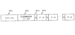
- FIG. 3 is an explanatory diagram illustrating an example of a frame format of a transmission signal.
- the frame format of the transmission signal includes a preamble 401, a transmission path estimation field 402, a guard interval (GI) 403, and data 404.
- GI guard interval
- the preamble 401 includes a waveform obtained by repeating a known signal waveform a plurality of times.
- the preamble 401 uses a waveform obtained by repeating a signal waveform of one unit a plurality of times with a signal waveform obtained by BPSK modulation of a 128-bit Golay sequence having excellent correlation characteristics as a unit.
- the transmission / reception apparatus obtains repetition of a known signal waveform by correlation detection, and uses it for synchronization processing including at least one of frame detection, gain control, and carrier frequency synchronization.
- the transmission path estimation field 402 includes a plurality of known signal waveforms, and is used for transmission path distortion estimation in the transmission / reception apparatus according to the present invention.
- the transmission path estimation field 402 uses a signal waveform obtained by BPSK modulation of a 128-bit Golay sequence and a complementary sequence of the Golay sequence.
- the guard interval 403 is inserted as a delimiter of the data 404.
- a known signal waveform for example, a signal obtained by BPSK modulation of a 64-bit Golay sequence is also used for the guard interval 403.
- the data 404 includes a symbol string obtained by PSK or QAM modulation of a data bit string that has been subjected to error correction coding for each block.
- the symbol sequence of the transmission signal digitally modulated using the frame format (signal format) described above is subjected to a root raised cosine filter as a transmission band limiting filter and converted to an analog baseband signal by a DA converter.
- the baseband signal is converted into a single carrier high frequency signal in a high frequency (RF) section (see FIG. 1) and transmitted from the antenna.
- RF high frequency
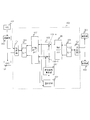
- FIG. 1 is a block diagram illustrating the overall configuration of the transmission / reception device 10.
- the transmission / reception device 10 includes an antenna 301, a high frequency unit (RF unit) 302, an AD converter 201, a synchronization unit 303, a distortion correction unit 102, a demodulation unit 304, a DA converter 101, and a modulation unit 103. It is.
- the RF unit 302 has a configuration on the transmission side for up-converting a signal that has been single-carrier modulated by the modulation unit 103, and a configuration on the reception side for down-converting a single-carrier high-frequency signal received by the antenna 301. including.
- the distortion correction unit 102 corrects transmission distortion characteristics received on the transmission side of the RF unit 302 by the symbol sequence digitally modulated (single carrier modulation) by the modulation unit 103 and outputs the correction to the DA converter 101.
- the DA converter 101 converts the output signal from the distortion correction unit 102 into an analog baseband signal.
- the transmission side of the RF unit 302 up-converts the analog baseband signal into a single carrier high-frequency signal and transmits it through the antenna 301.
- the receiving side of the RF unit 302 down-converts the single carrier high frequency signal received by the antenna 301 and converts it into a baseband signal.
- the reception side of the RF unit 302 outputs a baseband signal to the AD converter 201.
- the AD converter 201 samples an output signal from the reception side of the RF unit 302 and converts it into a digital signal.
- the synchronization unit 303 performs synchronization processing including at least one of frame detection, gain adjustment of the RF unit 302, and carrier frequency synchronization using the preamble 401 in the received signal of the converted digital signal.
- the distortion correction unit 102 estimates the transmission path distortion using the transmission path estimation field 402 according to the frame timing detected by the synchronization unit 303, corrects the distortion characteristics of the transmission path of the data 404 thereafter and the symbol string. Is output.
- the demodulator 304 receives the symbol sequence output from the distortion corrector 102, determines signal points, demodulates data, and reproduces transmission data.
- FIG. 2 is a block diagram showing the internal configuration of the distortion correction unit 102.
- the distortion correction unit 102 includes a switching unit C1, a parallel / serial conversion unit 104, a PN point inverse Fourier / Fourier conversion unit 105, a correction coefficient multiplication unit 106 (106-1 to 106-n), a correction unit,
- the configuration includes a coefficient calculation unit 107, a distortion estimation unit 202, an N-point Fourier / inverse Fourier transform unit 108, a serial / parallel conversion unit 109, and a switching unit C2.
- the switching unit C1 outputs a reception signal from the synchronization unit 303 to the parallel / serial conversion unit 104 during reception or calibration, and outputs a transmission signal from the parallel / serial conversion unit 104 to the DA converter 101 during transmission. Switch the transmission path.
- the parallel / serial converter 104 converts a serial signal into a parallel signal at the time of reception or calibration, and converts the parallel signal into a serial signal at the time of transmission.
- the PN point inverse Fourier / Fourier transform unit 105 as the first transform unit performs Fourier transform or inverse Fourier transform by using a P ⁇ N point frequency domain signal or time axis signal as a unit and by sign inversion of the rotor operation.
- the PN point inverse Fourier / Fourier transform unit 105 performs a Fourier transform using a time axis signal of P ⁇ N points as a unit and converts it to a frequency domain signal of P ⁇ N points.
- the PN point inverse Fourier / Fourier transform unit 105 performs inverse Fourier transform with a P ⁇ N point frequency domain signal as a unit to convert it into a P ⁇ N point time axis signal.
- the switching unit C2 outputs a reception signal from the serial / parallel conversion unit 109 to the demodulation unit 304 at the time of reception or calibration, and outputs a transmission signal from the modulation unit 103 to the serial / parallel conversion unit 109 at the time of transmission. Switch the transmission path.
- the serial / parallel converter 109 converts a parallel signal into a serial signal at the time of reception or calibration, and converts from a serial signal to a parallel signal at the time of transmission.
- the N-point Fourier / inverse Fourier transform unit 108 as the second transform unit performs Fourier transform or inverse Fourier transform in units of the N-point time axis signal or frequency domain signal so that it can be realized by sign inversion of the rotor operation. .
- the N-point Fourier / inverse Fourier transform unit 108 performs inverse Fourier transform in units of N-point frequency domain signals at the time of reception or calibration, and converts them into N-point time axis signals.
- the N-point Fourier / inverse Fourier transform unit 108 performs Fourier transform in units of N-point time axis signals at the time of transmission, and transforms them into N-point frequency domain signals.
- the distortion correction unit 102 can share each unit by changing the signal processing direction at any timing of transmission, reception, and calibration.
- reception distortion characteristic for example, a reference signal is input from the measuring device to the reception side of the RF unit 302, the reception distortion characteristic is measured using the same method as described later, and the reception distortion correction coefficient is calculated. It is possible to ask.
- FIG. 4 is a block diagram showing an internal configuration of the distortion correction unit 102 at the time of calibration of transmission distortion characteristics.
- the switching unit C1 is omitted.
- the DA converter 101 receives a reference signal having a known signal waveform, for example, from the outside of the transmission / reception device 10 and outputs it to the transmission side of the RF unit 302, and further loops back via the reception side of the RF unit 302. The same signal is input to the AD converter 201. That is, a loopback signal from the transmission side of the RF unit 302 to the reception side of the RF unit 302 is input to the RF unit 302.
- the reference signal may be any signal as long as it has a known signal waveform, for example, a modulated signal of the preamble 401 of the transmission signal.
- a sine wave signal having an arbitrary frequency may be used.
- it is a wideband signal that can measure the frequency characteristics of the signal band of the transmission signal, or a signal obtained by frequency sweeping a sine wave narrowband signal within the signal band.
- the AD converter 201 inputs and samples a reference signal obtained by looping back the RF unit 302, and outputs the sampled digital signal to the parallel / serial conversion unit 104 via the synchronization unit 303 and the switching unit C1.
- the parallel / serial converter 104 converts the input digital signal (serial signal) into a parallel signal and outputs the parallel signal to the PN point inverse Fourier / Fourier transformer 105.
- the PN point inverse Fourier / Fourier transform unit 105 performs Fourier transform on the time axis signal, which is an input signal from the parallel / serial conversion unit 104, and converts it into a frequency domain signal.
- the PN point inverse Fourier / Fourier transform unit 105 selects a signal band signal from the frequency domain signal and outputs the selected signal to the distortion estimation unit 202.
- the distortion estimation unit 202 corrects the frequency domain signal of the input signal band using the reception distortion characteristics of the RF unit 302 obtained in advance, and then corrects the frequency domain signal after correction and the frequency domain of a known reference signal.
- a difference vector from the signal is obtained for each frequency bin (range). The difference vector corresponds to the transmission distortion characteristic on the transmission side of the RF unit 302.
- the correction coefficient calculation unit 107 obtains a correction vector that is the inverse characteristic of the estimated transmission distortion characteristic based on the transmission distortion characteristic estimated by the distortion estimation unit 202, and stores the transmission distortion correction coefficient corresponding to the correction vector. . Furthermore, the correction coefficient calculation unit 107 may weight the correction vector for each frequency bin using the frequency domain characteristic of the root raised cosine filter obtained in advance as the transmission band limiting filter.
- FIG. 5 is a diagram in which signals of each part of the distortion correction unit 102 at the time of calibration are expressed by a spectrum.
- the reference signal for calibration is a signal having the same bandwidth fs (Hz) as that of the transmission signal.
- FIG. 5A shows the spectrum of the baseband signal input to the AD converter 201.
- the baseband signal is a complex signal and has a spectrum with a bandwidth fs (Hz) centering on a DC (0 Hz) component.
- FIG. 5B shows the spectrum of the signal after the AD converter 201 oversamples the baseband signal twice.
- the sampling rate is 2 fs (Hz), and aliasing occurs around fs (Hz).
- FIG. 5C shows a spectrum of a frequency domain signal obtained by converting a sample string by a 128-point FFT.
- the difference between the signal band characteristic 700 (see FIG. 5C) and the ideal frequency characteristic 701 (dotted line) is the transmission distortion characteristic with respect to the frequency bin of 64 points in the signal band. It becomes.
- the correction coefficient calculation unit 107 obtains a transmission distortion correction coefficient 702 (solid line) that is a reverse characteristic of the transmission distortion characteristic, and stores it in the correction coefficient calculation unit 107.
- the transmission signal x (t), the loopback reception signal r (t), the passband characteristic h_tx (t) on the transmission side of the RF unit 302, and the passband characteristic h_rx (t) on the reception side of the RF unit 302 are used.
- Equation (1) is obtained.
- x_ref (t) is a reference signal for calibration
- X_ref (f) is a value obtained by Fourier transforming x_ref (t)
- r_ref (t) and r_ref (t) are reference signals looped back to the reception side of the RF unit 302.
- the passband characteristic H (f) of the RF unit 302 is obtained by Expression (2).
- the communication band characteristic H_tx (f) on the transmission side of the RF unit 302 is obtained as represented by Equation (3).
- 1 / H_tx (f) is obtained as a transmission distortion correction coefficient 702 (see FIG. 7) which is a reverse characteristic of the transmission distortion characteristic by calibration of the distortion correction unit 102.
- FIG. 6 is a block diagram illustrating an internal configuration of the distortion correction unit 102 at the time of transmission.
- the switching unit C2 is omitted.
- the serial / parallel converter 109 receives a symbol string (serial signal) modulated at the symbol rate fs (Hz) from the modulator 103 via the switching unit C2, and converts it into a parallel signal every N symbols. To do.
- the N-point Fourier / inverse Fourier transform unit 108 performs Fourier transform on the input N-symbol signal, which is a parallel signal, and converts it into an N-point frequency domain signal that can be configured by a complex vector for each frequency bin.
- the N-point Fourier / inverse Fourier transform unit 108 converts the N-point frequency domain signal into the P-point (P> 1) oversampling necessary when the DA converter 101 converts the analog signal into an analog signal. Band extension to P ⁇ N points.
- the N-point Fourier / inverse Fourier transform unit 108 generates a complex vector in the signal band of the frequency bin in another band of the same frequency bin in order to generate an alias component of the signal band corresponding to oversampling. make a copy.
- the correction coefficient multiplying unit 106 applies the transmission distortion correction coefficient obtained by the correction coefficient calculating unit 107 to the frequency domain signal band-extended to P ⁇ N points by the N point Fourier / inverse Fourier transform unit 108 for each frequency bin. Multiply.
- the correction coefficient multiplication unit 106 outputs the multiplication result to the PN point inverse Fourier / Fourier transform unit 105.
- the PN point inverse Fourier / Fourier transform unit 105 performs inverse Fourier transform on the multiplication result from the correction coefficient multiplication unit 106, that is, the P ⁇ N point frequency domain signal multiplied by the transmission distortion correction coefficient, to obtain a time axis signal. Convert.
- the PN point inverse Fourier / Fourier transform unit 105 outputs the time axis signal to the parallel / serial conversion unit 104.
- the time axis signal is a sample sequence that has been oversampled P times with respect to the original N symbol sequence.
- a sample string of P ⁇ N samples is converted into a serial signal by the parallel / serial converter 104.
- the parallel / serial conversion unit 104 removes the first partial sample and the last few samples that are affected by the FFT and IFFT waveform truncation from the P ⁇ N samples, for example, a central P ⁇ N / 2 sample. Output a sample sequence.
- N symbols to be corrected are input while overlapping each other by N / 2 symbols from the symbol string input from the modulation unit 103 to the distortion correction unit 102. Thereby, the continuity of the sample sequence output from the distortion correction unit 102 is maintained.
- FIG. 7 is a diagram representing each signal in the distortion correction unit 102 by a spectrum.
- FIG. 7A shows the spectrum of the modulation signal from the modulation unit 103 at the symbol rate fs (Hz). Since the symbol rate fs (Hz) and the sample rate are the same sample sequence, the aliasing occurs at fs / 2 (Hz) in FIG.
- FIG. 7B shows a spectrum of a frequency domain signal obtained by transforming a sample string by 64-point FFT.
- FIG. 7C shows a spectrum of a frequency domain signal whose band is expanded by double oversampling for each frequency bin.
- the N-point Fourier / inverse Fourier transform unit 108 when the frequency band is expanded to 128 points by double oversampling, the N-point Fourier / inverse Fourier transform unit 108 generates an alias component of the signal in the original signal band with respect to the frequency bin that becomes the alias frequency. Copy the signal band component.
- FIG. 7D shows the spectrum of the signal of the transmission distortion correction coefficient 601.
- the transmission distortion correction coefficient 601 includes the characteristics of a root raised cosine filter (RRC filter)
- the multiplication also serves as a transmission band limiting filter.
- the PN point inverse Fourier / Fourier transform unit 105 performs inverse Fourier transform on the corrected frequency domain signal in 128-point IFFT to convert it into a time axis signal, and outputs it to the DA converter 101 via the switching unit C1.
- the input time-axis signal is converted into an analog signal in the DA converter 101, the spectrum of the baseband signal shown in FIG. 7F is obtained.
- the baseband signal is modulated using the single carrier frequency fc.
- FIG. 7G shows a spectrum of a frequency domain signal in which distortion on the transmission side of the RF unit is corrected.
- the correction coefficient multiplication unit 106 converts the frequency Rx filter characteristic C_filt (f) into the frequency domain signal X ′ (f) (see FIG. 7D) obtained by over-sampling the transmission signal x (t) by Fourier transform. ) And a correction coefficient 1 / H_tx (f) for correcting the passband characteristic on the transmission side of the RF unit 302, to obtain a signal X ′′ (f) represented by Expression (4) (FIG. 7E). reference).
- the PN point inverse Fourier / Fourier transform unit 105 performs inverse Fourier transform on the signal X ′′ (f) obtained by Equation (4) to obtain a time axis signal x ′′ (t) (see FIG. 7F).
- the time axis signal x ′′ (t) is transmitted from the antenna 301 via the transmission side of the RF unit 302.
- the signal x ′′ ′′ (t) is expressed by Equation (5).
- the transmission / reception device 10 can correct a signal distortion generated on the transmission side of the RF unit 302 and transmit a signal multiplied by a transmission filter (see FIG. 7G).
- FIG. 7G shows a spectrum of a signal in which the distortion of the RF transmitter is corrected.
- FIG. 8 is an explanatory diagram showing an example of a processing unit of a signal to be corrected.
- a sample (symbol) column 501 of the same sampling rate with the same symbol rate and sample rate is input.
- the serial / parallel converter 109 selects a sample sequence 502-1 of 64 samples corresponding to 64 symbols from the sample sequence 501.
- a 64-point Fourier transform and distortion correction are performed on each selected sample string 502 by the distortion correction unit 102, and the 128-sample (64 symbols) time-axis signal 503 is oversampled twice by the 128-point inverse Fourier transform. Converted.
- the partial sample sequence 504-1 of the center 64 samples (32 symbols) is selected and output.
- Sample columns 502-2 and 502-3 are similarly processed and converted into sample columns 504-2 and 504-3.
- the transmitting / receiving apparatus 10 performs FDE (Frequency Domain Equalization) using the distortion correction unit 102 as an equalizer at the time of reception, and measures the pass band of the RF unit at the time of calibration. Furthermore, according to the transmission / reception apparatus 10, it is used as a frequency domain filter that performs interpolation (oversampling) and predistortion (distortion correction) during transmission.
- FDE Frequency Domain Equalization
- the passband characteristic of the transmission RF circuit can be corrected with high accuracy without significantly increasing the circuit scale. Therefore, since the symbol rate is high, even the baseband signal having a wide signal bandwidth can correct the passband characteristic with high accuracy without increasing the circuit scale. Further, the processing clock speed can be lowered by parallelizing the signal processing.
- Each configuration according to the embodiment may be realized as an LSI which is an integrated circuit.
- the LSI may be made into one chip, or a part or all of each component may be made into one chip.
- LSI depending on the degree of integration, it may be referred to as IC, system LSI, super LSI, or ultra LSI.
- circuit integration is not limited to LSI, and circuit integration may be performed using a dedicated circuit or a general-purpose processor.
- an FPGA Field Programmable Gate Array
- a reconfigurable processor that can reconfigure the connection and setting of circuit cells inside the LSI may be used.
- these functional blocks can be performed using, for example, a DSP or a CPU. Further, these processing steps can be recorded on a recording medium as a program and executed.
- the present invention can be widely applied to all wireless communication devices including mobile communication that requires a small circuit scale and low power consumption as a transmission distortion compensation circuit used for single carrier communication.
- the present invention is a transmission / reception apparatus that transmits and receives a signal modulated using a single carrier transmission system, and has high symbol speed, so even a baseband signal having a wide signal bandwidth can be used without increasing the circuit scale.
- the passband characteristic can be corrected well, which is useful.
Abstract
The present invention accurately corrects passband characteristics without an increase in circuit scale, even for baseband signals having a signal bandwidth that spans a wide band as a result of a high-speed symbol rate. During transmission, a symbol sequence that has been modulated using a symbol rate (fs) (Hz) from a modulation unit (103) is input, and then converted into a parallel signal every N symbols in a serial/parallel conversion unit (109). The N symbol signal undergoes a Fourier transform in an N-point Fourier/inverse Fourier transform unit (108), and is converted into an N-point frequency domain signal. The N-point signal bandwidth is widened to P×N points. For each frequency bin, a correction coefficient multiplication unit (106) multiplies the frequency domain signal having the bandwidth widened to P×N points by a transmission distortion correction coefficient obtained in a correction coefficient calculation unit (107). The P×N-point frequency domain signal that has been multiplied by the transmission distortion correction coefficient undergoes an inverse Fourier transform in a PN-point inverse Fourier/Fourier transform unit (105) and is converted into a time axis signal.
Description
本発明は、シングルキャリア伝送方式を用いて変調された信号を送受信する送受信装置に関する。
The present invention relates to a transmission / reception apparatus for transmitting / receiving a signal modulated using a single carrier transmission system.
近年、高精細な画像(動画像及び静止画像を含む)又は音声を用いた種々の大容量コンテンツを含むデータを、無線通信を介してエンドユーザに提供するサービスが検討されている。
In recent years, services that provide high-definition images (including moving images and still images) or data including various large-capacity contents using audio to end users via wireless communication are being studied.
特に、数G(ギガ)ビットに及ぶ大容量のデータを高速に伝送するため、60GHz帯を含むミリ波帯を用いて、数Gbpsの高速伝送を行う無線通信システムが検討されている。特に、IEEE(Institute of Electrical and Electronics Engineering)において、無線PANとして例えばIEEE802.15.3c、又は無線LANとして例えばIEEE802.11adの規格標準化作業が行われている。
In particular, in order to transmit large-capacity data of several G (giga) bits at high speed, a wireless communication system that performs high-speed transmission of several Gbps using a millimeter wave band including a 60 GHz band has been studied. In particular, in IEEE (Institute of Electrical and Electronics Electronics), standardization work of, for example, IEEE 802.15.3c as a wireless PAN or IEEE 802.11ad as a wireless LAN is being performed.
例えば、IEEE802.11adにおいて検討されているミリ波帯を用いたシングルキャリア通信では、1.76Gシンボル/秒によってPSK又はQAM変調された信号を伝送する。1シンボル時間は約0.57nsecと短くなる。
For example, in single carrier communication using a millimeter wave band studied in IEEE802.11ad, a signal that is PSK or QAM modulated at 1.76 G symbols / second is transmitted. One symbol time is as short as about 0.57 nsec.
一方、変調されたベースバンド信号を60GHz帯にアップコンバートしてアンテナから送信する高周波(RF)回路では、広帯域な通信特性が求められる。信号帯域幅が1.76GHzとなり、広帯域であるので、信号歪みを起こさない送信のために、RF回路の通過帯域特性が信号の全帯域にわたって平坦であることが求められる。
On the other hand, in a radio frequency (RF) circuit that up-converts a modulated baseband signal to a 60 GHz band and transmits it from an antenna, broadband communication characteristics are required. Since the signal bandwidth is 1.76 GHz and is a wide band, the transmission band characteristic of the RF circuit is required to be flat over the entire band of the signal for transmission without causing signal distortion.
しかし、60GHzの高周波信号に変換するミキサー又はパワーアンプに、信号の全帯域にわたって平坦な通過帯域特性を持たせることは実際には難しい。
However, it is actually difficult for a mixer or power amplifier that converts to a high-frequency signal of 60 GHz to have a flat passband characteristic over the entire band of the signal.
RF回路における通過帯域特性の歪みを補正する方法として、デジタルベースバンド信号を用いてプレディストーションする方法が知られている。この方法では、予めRF回路の通過帯域特性を測定し、測定結果の逆特性となるデジタルフィルタ係数を求め、送信信号をフィルタリングすることで、RF回路通過時に通過帯域特性を平坦にするための補正が施される。
As a method for correcting distortion of passband characteristics in an RF circuit, a method of predistorting using a digital baseband signal is known. In this method, the passband characteristic of the RF circuit is measured in advance, a digital filter coefficient that is the inverse characteristic of the measurement result is obtained, and the transmission signal is filtered to correct the passband characteristic when passing through the RF circuit. Is given.
プレディストーションを用いる無線通信システムとして、例えば特許文献1、2が知られている。特許文献1に記載の無線通信装置は、RF回路を送信側から受信側へループバックした信号の周波数歪み特性を検出し、理想特性からの差分スペクトルを逆フーリエ変換した時間軸信号を保持し、送信時のFIRフィルタに加算することにより、歪みを補正する。
For example, Patent Documents 1 and 2 are known as wireless communication systems using predistortion. The wireless communication device described in Patent Document 1 detects a frequency distortion characteristic of a signal obtained by looping back an RF circuit from a transmission side to a reception side, holds a time axis signal obtained by performing an inverse Fourier transform on a difference spectrum from an ideal characteristic, Distortion is corrected by adding to the FIR filter at the time of transmission.
また、特許文献2に記載のデジタル無線通信装置は、周波数領域信号においてプレディストーションを行う。デジタル無線通信装置は、ゼロサンプル挿入によりL倍にオーバーサンプリングした時間軸信号をNポイントフーリエ変換し、周波数領域において重み付けする。デジタル無線通信装置は、重み付けの後、周波数binをシフトして中心周波数を変更し、Nポイント逆フーリエ変換により時間軸信号に変換して出力する。
Also, the digital wireless communication device described in Patent Document 2 performs predistortion on the frequency domain signal. The digital wireless communication device performs N-point Fourier transform on the time axis signal oversampled L times by inserting zero samples, and weights the signal in the frequency domain. After weighting, the digital wireless communication device shifts the frequency bin to change the center frequency, and converts it into a time axis signal by N-point inverse Fourier transform and outputs it.
しかしながら、上記従来の無線通信装置では、次の様な問題があった。具体的には、前述した従来技術では、送信信号のシンボルをDAコンバータにおいてオーバーサンプリング(インタポレーション)した信号に対し、プレディストーションフィルタを掛ける必要があった。
However, the conventional wireless communication apparatus has the following problems. Specifically, in the above-described prior art, it is necessary to apply a predistortion filter to a signal obtained by oversampling (interpolating) a symbol of a transmission signal in a DA converter.
即ち、上記従来の無線通信装置をミリ波の通信に適用しようとすると、例えば2倍オーバーサンプリングでも、3.52Gsps(サンプル/秒)の時間軸信号に対してデジタルフィルタを用いる必要がある。
That is, if the conventional wireless communication device is to be applied to millimeter wave communication, it is necessary to use a digital filter with respect to a time axis signal of 3.52 Gsps (samples / second) even with, for example, double oversampling.
インタポレーションフィルタ及びプレディストーションフィルタを用いて補正するRF回路の通過帯域特性の周波数分解能を高めるためには、数十タップのFIRフィルタが必要となり、回路規模が増大する。また、フィルタ演算には、高速な処理クロック速度が求められた。
In order to increase the frequency resolution of the passband characteristics of the RF circuit corrected using the interpolation filter and the predistortion filter, an FIR filter with several tens of taps is required, and the circuit scale increases. In addition, a high processing clock speed is required for the filter operation.
本発明は、この様な事情を考慮してなされたものであり、シンボル速度が高速であるために信号帯域幅が広帯域にわたるベースバンド信号でも、回路規模を増大せずに、通過帯域特性を高精度に補正する送受信装置を提供することを目的とする。
The present invention has been made in consideration of such circumstances, and since the symbol rate is high, even a baseband signal having a wide signal bandwidth has a high passband characteristic without increasing the circuit scale. It is an object of the present invention to provide a transmission / reception device that corrects accuracy.
本発明の送受信装置は、シングルキャリア伝送方式を用いて変調された信号を周波数変換する高周波部と、周波数領域信号に、前記高周波部の前記周波数変換における歪補正係数を乗算して歪補正する補正係数乗算部と、受信時に時間軸信号を周波数領域信号に変換し、送信時に前記補正係数乗算部によって歪補正された周波数領域信号を時間軸信号に変換する第1の変換部と、送信時に時間軸信号を周波数領域信号に変換し、受信時に前記補正係数乗算部によって歪補正された周波数領域信号を時間軸信号に変換する第2の変換部と、を備える。
The transmitting / receiving apparatus according to the present invention includes a high frequency unit that frequency-converts a signal modulated using a single carrier transmission method, and a correction that corrects distortion by multiplying a frequency domain signal by a distortion correction coefficient in the frequency conversion of the high frequency unit. A coefficient multiplier, a first converter that converts a time-axis signal into a frequency-domain signal at the time of reception, and converts a frequency-domain signal that has been distortion-corrected by the correction coefficient multiplier at the time of transmission into a time-axis signal; A second conversion unit that converts the axis signal into a frequency domain signal and converts the frequency domain signal that has been subjected to distortion correction by the correction coefficient multiplication unit at the time of reception into a time axis signal.
本発明によれば、送信時の歪補正において、受信時における補正係数乗算部、第1の変換部および第2の変換部を共用でき、回路規模を大幅に増大せずに、送信時、通過帯域特性を精度良く補正できる。
According to the present invention, in distortion correction at the time of transmission, the correction coefficient multiplication unit, the first conversion unit, and the second conversion unit at the time of reception can be shared, and transmission can be performed without greatly increasing the circuit scale. Band characteristics can be corrected with high accuracy.
本発明に係る送受信装置の実施形態について、図面を参照して説明する。本発明に係る送受信装置は、ミリ波帯の無線信号を送受信する送受信装置に適用される。
Embodiments of a transmitting / receiving apparatus according to the present invention will be described with reference to the drawings. The transmission / reception apparatus according to the present invention is applied to a transmission / reception apparatus that transmits and receives millimeter-wave band radio signals.
(信号フォーマット)
図3は、送信信号のフレームフォーマットの一例を表す説明図である。送信信号のフレームフォーマットは、プリアンブル401、伝送路推定用フィールド402、ガードインターバル(GI)403、及びデータ404を含む構成である。 (Signal format)
FIG. 3 is an explanatory diagram illustrating an example of a frame format of a transmission signal. The frame format of the transmission signal includes a preamble 401, a transmissionpath estimation field 402, a guard interval (GI) 403, and data 404.
図3は、送信信号のフレームフォーマットの一例を表す説明図である。送信信号のフレームフォーマットは、プリアンブル401、伝送路推定用フィールド402、ガードインターバル(GI)403、及びデータ404を含む構成である。 (Signal format)
FIG. 3 is an explanatory diagram illustrating an example of a frame format of a transmission signal. The frame format of the transmission signal includes a preamble 401, a transmission
プリアンブル401は、既知の信号波形を複数回繰り返した波形を含む。例えば、プリアンブル401には、相関特性に優れる128ビットのGolay系列をBPSK変調した信号波形を一単位として、一単位の信号波形を複数回繰り返した波形が用いられる。本発明に係る送受信装置は、既知の信号波形の繰り返しを相関検出により求め、フレームの検出、ゲイン制御、キャリア周波数同期のうち、少なくとも1つ以上を含む同期処理に用いる。
The preamble 401 includes a waveform obtained by repeating a known signal waveform a plurality of times. For example, the preamble 401 uses a waveform obtained by repeating a signal waveform of one unit a plurality of times with a signal waveform obtained by BPSK modulation of a 128-bit Golay sequence having excellent correlation characteristics as a unit. The transmission / reception apparatus according to the present invention obtains repetition of a known signal waveform by correlation detection, and uses it for synchronization processing including at least one of frame detection, gain control, and carrier frequency synchronization.
伝送路推定用フィールド402は、同様に複数個の既知の信号波形を含み、本発明に係る送受信装置において伝送路の歪み推定に用いられる。例えば、伝送路推定用フィールド402には、128bitのGolay系列とGolay系列の相補系列とをBPSK変調した信号波形が用いられる。
Similarly, the transmission path estimation field 402 includes a plurality of known signal waveforms, and is used for transmission path distortion estimation in the transmission / reception apparatus according to the present invention. For example, the transmission path estimation field 402 uses a signal waveform obtained by BPSK modulation of a 128-bit Golay sequence and a complementary sequence of the Golay sequence.
ガードインターバル403は、データ404の区切りとして挿入されている。ガードインターバル403にも、同様に既知の信号波形、例えば64bitのGolay系列をBPSK変調した信号が用いられる。
The guard interval 403 is inserted as a delimiter of the data 404. Similarly, a known signal waveform, for example, a signal obtained by BPSK modulation of a 64-bit Golay sequence is also used for the guard interval 403.
データ404は、ブロック単位毎に誤り訂正符号化されたデータビット列をPSK又はQAM変調したシンボル列を含む。
The data 404 includes a symbol string obtained by PSK or QAM modulation of a data bit string that has been subjected to error correction coding for each block.
前述のフレームフォーマット(信号フォーマット)を用いてデジタル変調された送信信号のシンボル列は、送信帯域制限フィルタとしてルートレイズドコサインフィルタに掛けられ、DAコンバータによりアナログベースバンド信号に変換される。ベースバンド信号は、高周波(RF)部(図1参照)においてシングルキャリア高周波信号に変換され、アンテナから送信される。
The symbol sequence of the transmission signal digitally modulated using the frame format (signal format) described above is subjected to a root raised cosine filter as a transmission band limiting filter and converted to an analog baseband signal by a DA converter. The baseband signal is converted into a single carrier high frequency signal in a high frequency (RF) section (see FIG. 1) and transmitted from the antenna.
(送受信装置の構成)
図1は、送受信装置10の全体構成を表すブロック図である。送受信装置10は、図1に表す様に、アンテナ301、高周波部(RF部)302、ADコンバータ201、同期部303、歪補正部102、復調部304、DAコンバータ101及び変調部103を含む構成である。 (Configuration of transceiver)
FIG. 1 is a block diagram illustrating the overall configuration of the transmission /reception device 10. As shown in FIG. 1, the transmission / reception device 10 includes an antenna 301, a high frequency unit (RF unit) 302, an AD converter 201, a synchronization unit 303, a distortion correction unit 102, a demodulation unit 304, a DA converter 101, and a modulation unit 103. It is.
図1は、送受信装置10の全体構成を表すブロック図である。送受信装置10は、図1に表す様に、アンテナ301、高周波部(RF部)302、ADコンバータ201、同期部303、歪補正部102、復調部304、DAコンバータ101及び変調部103を含む構成である。 (Configuration of transceiver)
FIG. 1 is a block diagram illustrating the overall configuration of the transmission /
なお、RF部302は、変調部103によりシングルキャリア変調された信号をアップコンバートするための送信側の構成と、アンテナ301により受信されたシングルキャリア高周波信号をダウンコンバートするための受信側の構成とを含む。
The RF unit 302 has a configuration on the transmission side for up-converting a signal that has been single-carrier modulated by the modulation unit 103, and a configuration on the reception side for down-converting a single-carrier high-frequency signal received by the antenna 301. including.
送信時、歪補正部102は、変調部103によりデジタル変調(シングルキャリア変調)されたシンボル列がRF部302の送信側において受ける送信歪特性を補正し、DAコンバータ101に出力する。
During transmission, the distortion correction unit 102 corrects transmission distortion characteristics received on the transmission side of the RF unit 302 by the symbol sequence digitally modulated (single carrier modulation) by the modulation unit 103 and outputs the correction to the DA converter 101.
DAコンバータ101は、歪補正部102からの出力信号を、アナログベースバンド信号に変換する。RF部302の送信側は、アナログベースバンド信号をシングルキャリア高周波信号にアップコンバートし、アンテナ301を介して送信する。
The DA converter 101 converts the output signal from the distortion correction unit 102 into an analog baseband signal. The transmission side of the RF unit 302 up-converts the analog baseband signal into a single carrier high-frequency signal and transmits it through the antenna 301.
受信時、RF部302の受信側は、アンテナ301により受信されたシングルキャリア高周波信号をダウンコンバートしてベースバンド信号に変換する。RF部302の受信側は、ベースバンド信号をADコンバータ201に出力する。ADコンバータ201は、RF部302の受信側からの出力信号をサンプリングしてデジタル信号に変換する。
At the time of reception, the receiving side of the RF unit 302 down-converts the single carrier high frequency signal received by the antenna 301 and converts it into a baseband signal. The reception side of the RF unit 302 outputs a baseband signal to the AD converter 201. The AD converter 201 samples an output signal from the reception side of the RF unit 302 and converts it into a digital signal.
同期部303は、変換されたデジタル信号の受信信号におけるプリアンブル401を用いて、フレームの検出、RF部302のゲイン調整、キャリア周波数同期のうち少なくとも1つ以上を含む同期処理を行う。
The synchronization unit 303 performs synchronization processing including at least one of frame detection, gain adjustment of the RF unit 302, and carrier frequency synchronization using the preamble 401 in the received signal of the converted digital signal.
歪補正部102は、同期部303において検出されたフレームタイミングに従い、伝送路推定用フィールド402を用いて伝送路歪みを推定し、これ以降のデータ404の伝送路の歪み特性を補正してシンボル列を出力する。
The distortion correction unit 102 estimates the transmission path distortion using the transmission path estimation field 402 according to the frame timing detected by the synchronization unit 303, corrects the distortion characteristics of the transmission path of the data 404 thereafter and the symbol string. Is output.
復調部304は、歪補正部102により出力されたシンボル列を入力し、信号点を判定してデータを復調し、送信データを再生する。
The demodulator 304 receives the symbol sequence output from the distortion corrector 102, determines signal points, demodulates data, and reproduces transmission data.
図2は、歪補正部102の内部構成を表すブロック図である。歪補正部102は、図2に表す様に、切替部C1、パラレル/シリアル変換部104、PNポイント逆フーリエ/フーリエ変換部105、補正係数乗算部106(106-1~106-n)、補正係数算出部107、歪推定部202、Nポイントフーリエ/逆フーリエ変換部108、シリアル/パラレル変換部109及び切替部C2を含む構成である。
FIG. 2 is a block diagram showing the internal configuration of the distortion correction unit 102. As shown in FIG. 2, the distortion correction unit 102 includes a switching unit C1, a parallel / serial conversion unit 104, a PN point inverse Fourier / Fourier conversion unit 105, a correction coefficient multiplication unit 106 (106-1 to 106-n), a correction unit, The configuration includes a coefficient calculation unit 107, a distortion estimation unit 202, an N-point Fourier / inverse Fourier transform unit 108, a serial / parallel conversion unit 109, and a switching unit C2.
切替部C1は、受信時あるいはキャリブレーション時には同期部303からの受信信号をパラレル/シリアル変換部104に出力し、送信時にはパラレル/シリアル変換部104からの送信信号をDAコンバータ101に出力するために、伝送路を切り替える。
The switching unit C1 outputs a reception signal from the synchronization unit 303 to the parallel / serial conversion unit 104 during reception or calibration, and outputs a transmission signal from the parallel / serial conversion unit 104 to the DA converter 101 during transmission. Switch the transmission path.
パラレル/シリアル変換部104は、受信時あるいはキャリブレーション時にはシリアル信号からパラレル信号に変換し、送信時にはパラレル信号からシリアル信号に変換する。
The parallel / serial converter 104 converts a serial signal into a parallel signal at the time of reception or calibration, and converts the parallel signal into a serial signal at the time of transmission.
第1の変換部としてのPNポイント逆フーリエ/フーリエ変換部105は、P×Nポイントの周波数領域信号又は時間軸信号を単位として、回転子演算の符号反転によって、フーリエ変換又は逆フーリエ変換する。
The PN point inverse Fourier / Fourier transform unit 105 as the first transform unit performs Fourier transform or inverse Fourier transform by using a P × N point frequency domain signal or time axis signal as a unit and by sign inversion of the rotor operation.
具体的には、PNポイント逆フーリエ/フーリエ変換部105は、受信時あるいはキャリブレーション時には、P×Nポイントの時間軸信号を単位としてフーリエ変換し、P×Nポイントの周波数領域信号に変換する。
Specifically, at the time of reception or calibration, the PN point inverse Fourier / Fourier transform unit 105 performs a Fourier transform using a time axis signal of P × N points as a unit and converts it to a frequency domain signal of P × N points.
また、PNポイント逆フーリエ/フーリエ変換部105は、送信時には、P×Nポイントの周波数領域信号を単位として逆フーリエ変換し、P×Nポイントの時間軸信号に変換する。
Further, at the time of transmission, the PN point inverse Fourier / Fourier transform unit 105 performs inverse Fourier transform with a P × N point frequency domain signal as a unit to convert it into a P × N point time axis signal.
切替部C2は、受信時あるいはキャリブレーション時にはシリアル/パラレル変換部109からの受信信号を復調部304に出力し、送信時には変調部103からの送信信号をシリアル/パラレル変換部109に出力するために、伝送路を切り替える。
The switching unit C2 outputs a reception signal from the serial / parallel conversion unit 109 to the demodulation unit 304 at the time of reception or calibration, and outputs a transmission signal from the modulation unit 103 to the serial / parallel conversion unit 109 at the time of transmission. Switch the transmission path.
シリアル/パラレル変換部109は、受信時あるいはキャリブレーション時にはパラレル信号からシリアル信号に変換し、送信時にはシリアル信号からパラレル信号に変換する。
The serial / parallel converter 109 converts a parallel signal into a serial signal at the time of reception or calibration, and converts from a serial signal to a parallel signal at the time of transmission.
第2の変換部としてのNポイントフーリエ/逆フーリエ変換部108は、回転子演算の符号反転によって実現可能に、Nポイントの時間軸信号又は周波数領域信号を単位として、フーリエ変換又は逆フーリエ変換する。
The N-point Fourier / inverse Fourier transform unit 108 as the second transform unit performs Fourier transform or inverse Fourier transform in units of the N-point time axis signal or frequency domain signal so that it can be realized by sign inversion of the rotor operation. .
具体的には、Nポイントフーリエ/逆フーリエ変換部108は、受信時あるいはキャリブレーション時には、Nポイントの周波数領域信号を単位として逆フーリエ変換し、Nポイントの時間軸信号に変換する。
More specifically, the N-point Fourier / inverse Fourier transform unit 108 performs inverse Fourier transform in units of N-point frequency domain signals at the time of reception or calibration, and converts them into N-point time axis signals.
また、Nポイントフーリエ/逆フーリエ変換部108は、送信時には、Nポイントの時間軸信号を単位としてフーリエ変換し、Nポイントの周波数領域信号に変換する。
Also, the N-point Fourier / inverse Fourier transform unit 108 performs Fourier transform in units of N-point time axis signals at the time of transmission, and transforms them into N-point frequency domain signals.
歪補正部102は、送信時、受信時及びキャリブレーション時のうち、いずれかのタイミングにおいて、信号の処理方向を変えることにより、各部を共用できる。
The distortion correction unit 102 can share each unit by changing the signal processing direction at any timing of transmission, reception, and calibration.
次に、歪補正部102の動作を詳細に説明する。
Next, the operation of the distortion correction unit 102 will be described in detail.
(キャリブレーション時の動作)
歪補正部102のキャリブレーション時における動作について説明する。キャリブレーションでは、RF部302の送信側における送信歪特性が測定され、送信歪特性を補正するための送信歪補正係数が求められる。なお、既に、RF部302の受信側における受信歪特性のキャリブレーションされており、受信歪特性を補正するための受信歪補正係数は予め求められているとする。 (Operation during calibration)
An operation during calibration of thedistortion correction unit 102 will be described. In the calibration, transmission distortion characteristics on the transmission side of the RF unit 302 are measured, and a transmission distortion correction coefficient for correcting the transmission distortion characteristics is obtained. It is assumed that the reception distortion characteristic on the reception side of the RF unit 302 has already been calibrated, and a reception distortion correction coefficient for correcting the reception distortion characteristic is obtained in advance.
歪補正部102のキャリブレーション時における動作について説明する。キャリブレーションでは、RF部302の送信側における送信歪特性が測定され、送信歪特性を補正するための送信歪補正係数が求められる。なお、既に、RF部302の受信側における受信歪特性のキャリブレーションされており、受信歪特性を補正するための受信歪補正係数は予め求められているとする。 (Operation during calibration)
An operation during calibration of the
なお、受信歪特性のキャリブレーションにおいては、例えば測定器からリファレンス信号をRF部302の受信側に入力し、後述する方法と同様の方法を用いて受信歪特性を測定し、受信歪補正係数を求めることが可能である。
In the calibration of the reception distortion characteristic, for example, a reference signal is input from the measuring device to the reception side of the RF unit 302, the reception distortion characteristic is measured using the same method as described later, and the reception distortion correction coefficient is calculated. It is possible to ask.
図4は、送信歪特性のキャリブレーション時における歪補正部102の内部構成を表すブロック図である。なお、図4において切替部C1は省略している。キャリブレーション時、DAコンバータ101は、既知の信号波形を持つリファレンス信号を例えば送受信装置10の外部から入力してRF部302の送信側に出力し、更にRF部302の受信側を介してループバックさせた同信号をADコンバータ201に入力する。即ち、RF部302には、同RF部302の送信側から同RF部302の受信側へのループバック信号が入力される。
FIG. 4 is a block diagram showing an internal configuration of the distortion correction unit 102 at the time of calibration of transmission distortion characteristics. In FIG. 4, the switching unit C1 is omitted. At the time of calibration, the DA converter 101 receives a reference signal having a known signal waveform, for example, from the outside of the transmission / reception device 10 and outputs it to the transmission side of the RF unit 302, and further loops back via the reception side of the RF unit 302. The same signal is input to the AD converter 201. That is, a loopback signal from the transmission side of the RF unit 302 to the reception side of the RF unit 302 is input to the RF unit 302.
ここで、リファレンス信号は既知の信号波形を持つ信号であれば、どのような信号でも良く、例えば送信信号のプリアンブル401の変調信号でもよい。あるいは任意の周波数の正弦波信号でもよい。好ましくは、送信信号の信号帯域の周波数特性が測定できるような広帯域信号、もしくは正弦波の狭帯域信号を信号帯域内において周波数スイープさせたような信号であることが望ましい。
Here, the reference signal may be any signal as long as it has a known signal waveform, for example, a modulated signal of the preamble 401 of the transmission signal. Alternatively, a sine wave signal having an arbitrary frequency may be used. Preferably, it is a wideband signal that can measure the frequency characteristics of the signal band of the transmission signal, or a signal obtained by frequency sweeping a sine wave narrowband signal within the signal band.
ADコンバータ201は、RF部302をループバックしたリファレンス信号を入力してサンプリングし、同期部303及び切替部C1を介して、サンプリング後のデジタル信号をパラレル/シリアル変換部104に出力する。
The AD converter 201 inputs and samples a reference signal obtained by looping back the RF unit 302, and outputs the sampled digital signal to the parallel / serial conversion unit 104 via the synchronization unit 303 and the switching unit C1.
パラレル/シリアル変換部104は、入力されたデジタル信号(シリアル信号)をパラレル信号に変換し、PNポイント逆フーリエ/フーリエ変換部105に出力する。
The parallel / serial converter 104 converts the input digital signal (serial signal) into a parallel signal and outputs the parallel signal to the PN point inverse Fourier / Fourier transformer 105.
PNポイント逆フーリエ/フーリエ変換部105は、パラレル/シリアル変換部104からの入力信号である時間軸信号に対してフーリエ変換し、周波数領域信号に変換する。PNポイント逆フーリエ/フーリエ変換部105は、周波数領域信号から信号帯域の信号を選択して歪推定部202に出力する。
The PN point inverse Fourier / Fourier transform unit 105 performs Fourier transform on the time axis signal, which is an input signal from the parallel / serial conversion unit 104, and converts it into a frequency domain signal. The PN point inverse Fourier / Fourier transform unit 105 selects a signal band signal from the frequency domain signal and outputs the selected signal to the distortion estimation unit 202.
歪推定部202は、入力された信号帯域の周波数領域信号を、予め求められているRF部302の受信歪特性を用いて補正した後、補正後の周波数領域信号と既知のリファレンス信号の周波数領域信号との差分ベクトルを周波数bin(範囲)毎に求める。差分ベクトルは、RF部302の送信側における送信歪特性に相当する。
The distortion estimation unit 202 corrects the frequency domain signal of the input signal band using the reception distortion characteristics of the RF unit 302 obtained in advance, and then corrects the frequency domain signal after correction and the frequency domain of a known reference signal. A difference vector from the signal is obtained for each frequency bin (range). The difference vector corresponds to the transmission distortion characteristic on the transmission side of the RF unit 302.
補正係数算出部107は、歪推定部202によって推定された送信歪特性を基に、推定された送信歪特性の逆特性となる補正ベクトルを求め、補正ベクトルに対応する送信歪補正係数を保存する。更に、補正係数算出部107は、送信帯域制限フィルタとして予め求められたルートレイズドコサインフィルタの周波数領域特性を用いて、周波数bin毎に、補正ベクトルに重み付けをしても良い。
The correction coefficient calculation unit 107 obtains a correction vector that is the inverse characteristic of the estimated transmission distortion characteristic based on the transmission distortion characteristic estimated by the distortion estimation unit 202, and stores the transmission distortion correction coefficient corresponding to the correction vector. . Furthermore, the correction coefficient calculation unit 107 may weight the correction vector for each frequency bin using the frequency domain characteristic of the root raised cosine filter obtained in advance as the transmission band limiting filter.
図5は、キャリブレーション時における歪補正部102の各部の信号をスペクトルによって表現した図である。キャリブレーション用のリファレンス信号は、送信信号と同じ帯域幅fs(Hz)を有する信号とする。
FIG. 5 is a diagram in which signals of each part of the distortion correction unit 102 at the time of calibration are expressed by a spectrum. The reference signal for calibration is a signal having the same bandwidth fs (Hz) as that of the transmission signal.
図5(A)は、ADコンバータ201に入力されたベースバンド信号のスペクトルを表す。ベースバンド信号は、複素信号であり、DC(0Hz)成分を中心に帯域幅fs(Hz)のスペクトルとなる。
FIG. 5A shows the spectrum of the baseband signal input to the AD converter 201. The baseband signal is a complex signal and has a spectrum with a bandwidth fs (Hz) centering on a DC (0 Hz) component.
図5(B)は、ADコンバータ201がベースバンド信号を2倍オーバーサンプリングした後の信号のスペクトルを表す。サンプリング速度が2fs(Hz)であり、fs(Hz)を中心に折り返し(エイリアシング)が生じている。
FIG. 5B shows the spectrum of the signal after the AD converter 201 oversamples the baseband signal twice. The sampling rate is 2 fs (Hz), and aliasing occurs around fs (Hz).
図5(C)は、サンプル列を128ポイントのFFTによって変換した周波数領域信号のスペクトルを表す。横軸は、2fs(Hz)を128ポイントに離散化した周波数bin(k=0~127)を表す。信号帯域は、k=0~31と、k=96~127の周波数binに存在する。
FIG. 5C shows a spectrum of a frequency domain signal obtained by converting a sample string by a 128-point FFT. The horizontal axis represents a frequency bin (k = 0 to 127) obtained by discretizing 2 fs (Hz) into 128 points. The signal band exists in the frequency bin of k = 0 to 31 and k = 96 to 127.
図5(D)に表す様に、信号帯域の64ポイント分の周波数binに対し、信号帯域特性700(図5(C)参照)と理想の周波数特性701(点線)との差分が送信歪特性となる。補正係数算出部107は、送信歪特性の逆特性となる送信歪補正係数702(実線)を求め、補正係数算出部107に記憶する。
As shown in FIG. 5D, the difference between the signal band characteristic 700 (see FIG. 5C) and the ideal frequency characteristic 701 (dotted line) is the transmission distortion characteristic with respect to the frequency bin of 64 points in the signal band. It becomes. The correction coefficient calculation unit 107 obtains a transmission distortion correction coefficient 702 (solid line) that is a reverse characteristic of the transmission distortion characteristic, and stores it in the correction coefficient calculation unit 107.
ここで、数式を用いて、歪補正部102におけるキャリブレーションの動作を説明する。
Here, the calibration operation in the distortion correction unit 102 will be described using mathematical expressions.
送信信号x(t)、ループバック受信信号r(t)、RF部302の送信側の通過帯域特性h_tx(t)、RF部302の受信側の通過帯域特性h_rx(t)とする。
Suppose that the transmission signal x (t), the loopback reception signal r (t), the passband characteristic h_tx (t) on the transmission side of the RF unit 302, and the passband characteristic h_rx (t) on the reception side of the RF unit 302 are used.
更に、送信信号x(t)、ループバック受信信号r(t)、RF部302の送信側の通過帯域特性h_tx(t)、RF部302の受信側の通過帯域特性h_rx(t)をフーリエ変換した値をそれぞれX(f)、R(f)、H_tx(f)、H_rx(f)とすると、数式(1)が得られる。
Further, Fourier transform is performed on the transmission signal x (t), the loopback reception signal r (t), the passband characteristic h_tx (t) on the transmission side of the RF unit 302, and the passband characteristic h_rx (t) on the reception side of the RF unit 302. Assuming that the obtained values are X (f), R (f), H_tx (f), and H_rx (f), Equation (1) is obtained.

また、キャリブレーション用リファレンス信号をx_ref(t)、x_ref(t)がフーリエ変換された値をX_ref(f)、RF部302の受信側にループバックしたリファレンス信号をr_ref(t)、r_ref(t)がフーリエ変換された値をR_ref(f)とする。RF部302の通過帯域特性H(f)は、数式(2)により求められる。
Further, x_ref (t) is a reference signal for calibration, X_ref (f) is a value obtained by Fourier transforming x_ref (t), and r_ref (t) and r_ref (t) are reference signals looped back to the reception side of the RF unit 302. ) Is R_ref (f). The passband characteristic H (f) of the RF unit 302 is obtained by Expression (2).
ここで、予め求められたRF部の受信側における通過帯域特性H_rx(f)を用いると、RF部302の送信側における通信帯域特性H_tx(f)が、数式(3)に表す様に求められる。
Here, when the passband characteristic H_rx (f) on the reception side of the RF unit obtained in advance is used, the communication band characteristic H_tx (f) on the transmission side of the RF unit 302 is obtained as represented by Equation (3). .

すなわち、歪補正部102のキャリブレーションにより、送信歪特性の逆特性となる送信歪補正係数702(図7参照)として、1/H_tx(f)が求められる。
That is, 1 / H_tx (f) is obtained as a transmission distortion correction coefficient 702 (see FIG. 7) which is a reverse characteristic of the transmission distortion characteristic by calibration of the distortion correction unit 102.
(送信時の動作)
次に、歪補正部102がキャリブレーション時に求められた送信歪補正係数を用いて送信信号を補正する動作を説明する。図6は、送信時における歪補正部102の内部構成を表すブロック図である。なお、図6において切替部C2は省略している。 (Operation when sending)
Next, an operation in which thedistortion correction unit 102 corrects a transmission signal using a transmission distortion correction coefficient obtained at the time of calibration will be described. FIG. 6 is a block diagram illustrating an internal configuration of the distortion correction unit 102 at the time of transmission. In FIG. 6, the switching unit C2 is omitted.
次に、歪補正部102がキャリブレーション時に求められた送信歪補正係数を用いて送信信号を補正する動作を説明する。図6は、送信時における歪補正部102の内部構成を表すブロック図である。なお、図6において切替部C2は省略している。 (Operation when sending)
Next, an operation in which the
送信時、シリアル/パラレル変換部109は、切替部C2を介して、変調部103からシンボル速度fs(Hz)において変調されたシンボル列(シリアル信号)を入力し、Nシンボル毎にパラレル信号に変換する。
At the time of transmission, the serial / parallel converter 109 receives a symbol string (serial signal) modulated at the symbol rate fs (Hz) from the modulator 103 via the switching unit C2, and converts it into a parallel signal every N symbols. To do.
Nポイントフーリエ/逆フーリエ変換部108は、入力されたパラレル信号であるNシンボルの信号をフーリエ変換し、周波数bin毎の複素ベクトルによって構成可能なNポイントの周波数領域信号に変換する。
The N-point Fourier / inverse Fourier transform unit 108 performs Fourier transform on the input N-symbol signal, which is a parallel signal, and converts it into an N-point frequency domain signal that can be configured by a complex vector for each frequency bin.
更に、Nポイントフーリエ/逆フーリエ変換部108は、DAコンバータ101がアナログ信号に変換する場合に必要なP倍(P>1)のオーバーサンプリングを可能とするために、Nポイントの周波数領域信号をP×Nポイントに帯域拡張する。
Further, the N-point Fourier / inverse Fourier transform unit 108 converts the N-point frequency domain signal into the P-point (P> 1) oversampling necessary when the DA converter 101 converts the analog signal into an analog signal. Band extension to P × N points.
具体的には、Nポイントフーリエ/逆フーリエ変換部108は、オーバーサンプリングに相当する信号帯域のエイリアス成分を生成するために、周波数binの信号帯域における複素ベクトルを、同周波数binの他の帯域にコピーする。
Specifically, the N-point Fourier / inverse Fourier transform unit 108 generates a complex vector in the signal band of the frequency bin in another band of the same frequency bin in order to generate an alias component of the signal band corresponding to oversampling. make a copy.
補正係数乗算部106は、Nポイントフーリエ/逆フーリエ変換部108によりP×Nポイントに帯域拡張された周波数領域信号に、補正係数算出部107により求められた送信歪補正係数を、周波数bin毎に乗算する。補正係数乗算部106は、乗算結果をPNポイント逆フーリエ/フーリエ変換部105に出力する。
The correction coefficient multiplying unit 106 applies the transmission distortion correction coefficient obtained by the correction coefficient calculating unit 107 to the frequency domain signal band-extended to P × N points by the N point Fourier / inverse Fourier transform unit 108 for each frequency bin. Multiply. The correction coefficient multiplication unit 106 outputs the multiplication result to the PN point inverse Fourier / Fourier transform unit 105.
PNポイント逆フーリエ/フーリエ変換部105は、補正係数乗算部106からの乗算結果、即ち、送信歪補正係数が乗算されたP×Nポイントの周波数領域信号を、逆フーリエ変換し、時間軸信号に変換する。PNポイント逆フーリエ/フーリエ変換部105は、時間軸信号をパラレル/シリアル変換部104に出力する。
The PN point inverse Fourier / Fourier transform unit 105 performs inverse Fourier transform on the multiplication result from the correction coefficient multiplication unit 106, that is, the P × N point frequency domain signal multiplied by the transmission distortion correction coefficient, to obtain a time axis signal. Convert. The PN point inverse Fourier / Fourier transform unit 105 outputs the time axis signal to the parallel / serial conversion unit 104.
時間軸信号は、元のNシンボルのシンボル列に対してP倍のオーバーサンプリングされたサンプル列である。P×Nサンプルのサンプル列は、パラレル/シリアル変換部104においてシリアル信号に変換される。
The time axis signal is a sample sequence that has been oversampled P times with respect to the original N symbol sequence. A sample string of P × N samples is converted into a serial signal by the parallel / serial converter 104.
パラレル/シリアル変換部104は、P×Nサンプルのうち、FFT及びIFFTの波形打ち切りの影響を受ける先頭及び最後の数サンプルを除去した中央の部分サンプル列、例えば中央のP×N/2サンプルのサンプル列を出力する。
The parallel / serial conversion unit 104 removes the first partial sample and the last few samples that are affected by the FFT and IFFT waveform truncation from the P × N samples, for example, a central P × N / 2 sample. Output a sample sequence.
なお、送受信装置10において、変調部103から歪補正部102に入力されたシンボル列から補正の対象とするNシンボルをN/2シンボルずつオーバーラップさせながら入力する。これにより、歪補正部102から出力されるサンプル列の連続性が保たれる。
In the transmission / reception apparatus 10, N symbols to be corrected are input while overlapping each other by N / 2 symbols from the symbol string input from the modulation unit 103 to the distortion correction unit 102. Thereby, the continuity of the sample sequence output from the distortion correction unit 102 is maintained.
図7は、歪補正部102内の各信号をスペクトルによって表現した図である。図7(A)は、変調部103からのシンボル速度fs(Hz)の変調信号のスペクトルを表す。シンボル速度fs(Hz)とサンプル速度とが等しいサンプル列であるので、図7(A)においてfs/2(Hz)において折り返しが発生している。
FIG. 7 is a diagram representing each signal in the distortion correction unit 102 by a spectrum. FIG. 7A shows the spectrum of the modulation signal from the modulation unit 103 at the symbol rate fs (Hz). Since the symbol rate fs (Hz) and the sample rate are the same sample sequence, the aliasing occurs at fs / 2 (Hz) in FIG.
図7(B)は、サンプル列を64ポイントのFFTによって変換した周波数領域信号のスペクトルを表す。横軸はfs(Hz)を64ポイントに離散化した周波数bin(k=0~63)を表す。
FIG. 7B shows a spectrum of a frequency domain signal obtained by transforming a sample string by 64-point FFT. The horizontal axis represents the frequency bin (k = 0 to 63) obtained by discretizing fs (Hz) into 64 points.
図7(C)は、周波数bin毎の、2倍のオーバーサンプリングによって帯域拡張した周波数領域信号のスペクトルを表す。図7(C)に表す様に、Nポイントフーリエ/逆フーリエ変換部108は、DAコンバータ101が2倍(P=2)のオーバーサンプリングを行うために、Nポイントの周波数領域信号を帯域拡張する。
FIG. 7C shows a spectrum of a frequency domain signal whose band is expanded by double oversampling for each frequency bin. As shown in FIG. 7C, the N-point Fourier / inverse Fourier transform unit 108 extends the band of the N-point frequency domain signal so that the DA converter 101 performs oversampling twice (P = 2). .
即ち、Nポイントフーリエ/逆フーリエ変換部108は、2倍オーバーサンプリングによって周波数帯域が128ポイントに広がる場合、元の信号帯域の信号のエイリアス成分を生成するために、エイリアス周波数となる周波数binに対して信号帯域成分をコピーする。
That is, when the frequency band is expanded to 128 points by double oversampling, the N-point Fourier / inverse Fourier transform unit 108 generates an alias component of the signal in the original signal band with respect to the frequency bin that becomes the alias frequency. Copy the signal band component.
図7(D)は、送信歪補正係数601の信号のスペクトルである。図7(D)に表す様に、補正係数乗算部106によりオーバーサンプリングされた128ポイントの周波数領域信号に送信歪補正係数601が乗算されると、送信歪が補正された後の周波数領域信号が得られる(図7(E)参照)。図7(E)は、送信歪補正係数の乗算後の周波数領域信号のスペクトルを表す。送信歪補正係数601には、ルートレイズドコサインフィルタ(RRCフィルタ)の特性も含まれている場合、上記乗算は送信帯域制限フィルタの役割も果たす。
FIG. 7D shows the spectrum of the signal of the transmission distortion correction coefficient 601. As shown in FIG. 7D, when the 128-point frequency domain signal oversampled by the correction coefficient multiplication unit 106 is multiplied by the transmission distortion correction coefficient 601, the frequency domain signal after the transmission distortion is corrected is obtained. Is obtained (see FIG. 7E). FIG. 7E shows the spectrum of the frequency domain signal after multiplication by the transmission distortion correction coefficient. When the transmission distortion correction coefficient 601 includes the characteristics of a root raised cosine filter (RRC filter), the multiplication also serves as a transmission band limiting filter.
PNポイント逆フーリエ/フーリエ変換部105は、補正された周波数領域信号を128ポイントIFFTにおいて逆フーリエ変換して時間軸信号に変換し、切替部C1を介してDAコンバータ101に出力する。DAコンバータ101において、入力された時間軸信号をアナログ信号に変換すると、図7(F)に表すベースバンド信号のスペクトルが得られる。
The PN point inverse Fourier / Fourier transform unit 105 performs inverse Fourier transform on the corrected frequency domain signal in 128-point IFFT to convert it into a time axis signal, and outputs it to the DA converter 101 via the switching unit C1. When the input time-axis signal is converted into an analog signal in the DA converter 101, the spectrum of the baseband signal shown in FIG. 7F is obtained.
更に、RF部302において、図7(G)に表すように、ベースバンド信号はシングルキャリア周波数fcを用いて変調される。図7(G)は、RF部の送信側における歪みが補正された周波数領域信号のスペクトルを表す。
Further, in the RF unit 302, as shown in FIG. 7G, the baseband signal is modulated using the single carrier frequency fc. FIG. 7G shows a spectrum of a frequency domain signal in which distortion on the transmission side of the RF unit is corrected.
ここで、数式を用いて、歪補正部102における送信時の送信歪補正の動作を説明する。
Here, the operation of transmission distortion correction at the time of transmission in the distortion correction unit 102 will be described using mathematical expressions.
補正係数乗算部106は、送信信号x(t)をフーリエ変換してオーバーサンプリングした周波数領域信号X’(f)に(図7(D)参照)、送信RRCフィルタ特性の周波数領域表現C_filt(f)と、RF部302の送信側の通過帯域特性を補正する補正係数1/H_tx(f)とを乗算し、数式(4)に表す信号X’’(f)を得る(図7(E)参照)。
The correction coefficient multiplication unit 106 converts the frequency Rx filter characteristic C_filt (f) into the frequency domain signal X ′ (f) (see FIG. 7D) obtained by over-sampling the transmission signal x (t) by Fourier transform. ) And a correction coefficient 1 / H_tx (f) for correcting the passband characteristic on the transmission side of the RF unit 302, to obtain a signal X ″ (f) represented by Expression (4) (FIG. 7E). reference).

PNポイント逆フーリエ/フーリエ変換部105は、数式(4)によって求められた信号X’’(f)を逆フーリエ変換して時間軸信号x’’(t)(図7(F)参照)を求める。時間軸信号x’’(t)は、RF部302の送信側を介してアンテナ301から送信される。信号x’’’(t)は、数式(5)により表される。
The PN point inverse Fourier / Fourier transform unit 105 performs inverse Fourier transform on the signal X ″ (f) obtained by Equation (4) to obtain a time axis signal x ″ (t) (see FIG. 7F). Ask. The time axis signal x ″ (t) is transmitted from the antenna 301 via the transmission side of the RF unit 302. The signal x ″ ″ (t) is expressed by Equation (5).

ただし、*は畳み込み演算を表す。信号x’’’(t)をフーリエ変換して周波数領域によって表すと、数式(6)により表される。
However, * represents a convolution operation. When the signal x ′ ″ (t) is Fourier-transformed and expressed in the frequency domain, it is expressed by Equation (6).

送受信装置10は、RF部302の送信側において生じる信号の歪みを補正し、送信フィルタを乗じた信号を送信できる(図7(G)参照)。図7(G)は、RF送信部の歪みが補正された信号のスペクトルを表す。
The transmission / reception device 10 can correct a signal distortion generated on the transmission side of the RF unit 302 and transmit a signal multiplied by a transmission filter (see FIG. 7G). FIG. 7G shows a spectrum of a signal in which the distortion of the RF transmitter is corrected.
図8は、補正の対象とする信号の処理単位の一例を表す説明図である。図8では、シンボル速度とサンプル速度とが等しい等倍サンプリングのサンプル(シンボル)列501が入力される。補正対象の処理単位をN=64シンボルとする。
FIG. 8 is an explanatory diagram showing an example of a processing unit of a signal to be corrected. In FIG. 8, a sample (symbol) column 501 of the same sampling rate with the same symbol rate and sample rate is input. The processing unit to be corrected is N = 64 symbols.
シリアル/パラレル変換部109は、サンプル列501から64シンボル分に相当する64サンプルのサンプル列502-1を選択する。シリアル/パラレル変換部109は、N/2=32シンボル(32サンプル)ずつオーバーラップさせたサンプル列502(502-1、502-2、502-3)を処理単位として選択する。
The serial / parallel converter 109 selects a sample sequence 502-1 of 64 samples corresponding to 64 symbols from the sample sequence 501. The serial / parallel converter 109 selects a sample string 502 (502-1, 502-2, 502-3) that is overlapped by N / 2 = 32 symbols (32 samples) as a processing unit.
選択された各サンプル列502に対し、歪補正部102によって64ポイントフーリエ変換及び歪補正が行われ、128ポイント逆フーリエ変換により2倍オーバーサンプリングされた128サンプル(64シンボル)の時間軸信号503に変換される。
A 64-point Fourier transform and distortion correction are performed on each selected sample string 502 by the distortion correction unit 102, and the 128-sample (64 symbols) time-axis signal 503 is oversampled twice by the 128-point inverse Fourier transform. Converted.
ここから、中央64サンプル(32シンボル)の部分サンプル列504-1が選択されて出力される。サンプル列502-2、502-3も同様に処理され、サンプル列504-2、504-3に変換される。
From here, the partial sample sequence 504-1 of the center 64 samples (32 symbols) is selected and output. Sample columns 502-2 and 502-3 are similarly processed and converted into sample columns 504-2 and 504-3.
これらのサンプル列504-1、504-2、504-3が連結され、シンボル速度に対してP=2倍の速度によってオーバーサンプリングされたサンプル列505は、連続性が保たれたまま出力される。
These sample sequences 504-1, 504-2, and 504-3 are connected, and a sample sequence 505 that is oversampled at a rate P = 2 times the symbol rate is output while maintaining continuity. .
以上の様に、本発明に係る送受信装置10は、歪補正部102を、受信時に等化器として用いてFDE(Frequency Domain Equalization)を行い、キャリブレーション時にはRF部の通過帯域を測定する。更に、送受信装置10によれば、送信時にはインタポレーション(オーバーサンプリング)とプレディストーション(歪補正)とを行う周波数領域フィルタとして用いる。
As described above, the transmitting / receiving apparatus 10 according to the present invention performs FDE (Frequency Domain Equalization) using the distortion correction unit 102 as an equalizer at the time of reception, and measures the pass band of the RF unit at the time of calibration. Furthermore, according to the transmission / reception apparatus 10, it is used as a frequency domain filter that performs interpolation (oversampling) and predistortion (distortion correction) during transmission.
これにより、送受信装置10によれば、回路規模を大幅に増大せずに、精度良く送信RF回路の通過帯域特性を補正できる。従って、シンボル速度が高速であるために信号帯域幅が広帯域にわたるベースバンド信号でも、回路規模を増大せずに、精度良く通過帯域特性を補正できる。また、信号処理を並列化することによって処理クロック速度を下げることができる。
Thereby, according to the transmission / reception apparatus 10, the passband characteristic of the transmission RF circuit can be corrected with high accuracy without significantly increasing the circuit scale. Therefore, since the symbol rate is high, even the baseband signal having a wide signal bandwidth can correct the passband characteristic with high accuracy without increasing the circuit scale. Further, the processing clock speed can be lowered by parallelizing the signal processing.
以上、図面を参照しながら各種の実施形態について説明したが、本発明はかかる例に限定されないことは言うまでもない。当業者であれば、特許請求の範囲に記載された範疇内において、各種の変更例または修正例に想到し得ることは明らかであり、それらについても当然に本発明の技術的範囲に属するものと了解される。
Although various embodiments have been described above with reference to the drawings, it goes without saying that the present invention is not limited to such examples. It will be apparent to those skilled in the art that various changes and modifications can be made within the scope of the claims, and these are naturally within the technical scope of the present invention. Understood.
なお、実施の形態にかかる各構成は、集積回路であるLSIとして実現されても良い。LSIは、1チップ化されてもよいし、各構成の一部または全てを含んで1チップ化しても良い。ここでは、LSIと称したが、集積度の違いによっては、IC、システムLSI、スーパーLSI、ウルトラLSIと称呼されることもある。
Each configuration according to the embodiment may be realized as an LSI which is an integrated circuit. The LSI may be made into one chip, or a part or all of each component may be made into one chip. Although referred to here as LSI, depending on the degree of integration, it may be referred to as IC, system LSI, super LSI, or ultra LSI.
また、集積回路化の手法は、LSIに限られず、専用回路または汎用プロセッサを用いて集積回路化してもよい。また、LSI製造後にプログラムすることが可能なFPGA(Field Programmable Gate Array)、LSI内部の回路セルの接続及び設定を再構成可能なリコンフィギュラブル・プロセッサを用いても良い。
Further, the method of circuit integration is not limited to LSI, and circuit integration may be performed using a dedicated circuit or a general-purpose processor. Further, an FPGA (Field Programmable Gate Array) that can be programmed after LSI manufacturing, or a reconfigurable processor that can reconfigure the connection and setting of circuit cells inside the LSI may be used.
また、これらの機能ブロックの演算は、例えばDSP又はCPUを用いて演算できる。さらに、これらの処理ステップはプログラムとして記録媒体に記録して実行できる。
Further, the calculation of these functional blocks can be performed using, for example, a DSP or a CPU. Further, these processing steps can be recorded on a recording medium as a program and executed.
さらには、半導体技術の進歩または派生する別技術によりLSIに置き換わる集積回路化の技術が登場すれば、当然、別技術を用いて機能ブロックを集積化してもよい。
Furthermore, if integrated circuit technology that replaces LSI emerges as a result of advances in semiconductor technology or other derived technologies, it is natural that functional blocks may be integrated using other technologies.
また、上記実施形態では、ミリ波帯の無線信号を送受信する場合を示したが、センチメートル波帯を含む無線信号においても、本発明は同様に適用可能である。
In the above-described embodiment, a case where a radio signal in the millimeter wave band is transmitted / received has been described. However, the present invention can be similarly applied to a radio signal including a centimeter wave band.
また、本発明は、シングルキャリア通信に用いる送信歪補償回路として、小回路規模・低消費電力が要求されるモバイル通信を含む無線通信機器全般に広く適用できる。
Further, the present invention can be widely applied to all wireless communication devices including mobile communication that requires a small circuit scale and low power consumption as a transmission distortion compensation circuit used for single carrier communication.
なお、本出願は、2011年3月30日出願の日本特許出願(特願2011-075832)に基づくものであり、その内容はここに参照として取り込まれる。
Note that this application is based on a Japanese patent application filed on March 30, 2011 (Japanese Patent Application No. 2011-075832), the contents of which are incorporated herein by reference.
本発明は、シングルキャリア伝送方式を用いて変調された信号を送受信する送受信装置において、シンボル速度が高速であるために信号帯域幅が広帯域にわたるベースバンド信号でも、回路規模を増大せずに、精度良く通過帯域特性を補正でき、有用である。
The present invention is a transmission / reception apparatus that transmits and receives a signal modulated using a single carrier transmission system, and has high symbol speed, so even a baseband signal having a wide signal bandwidth can be used without increasing the circuit scale. The passband characteristic can be corrected well, which is useful.
10 送受信装置
101 DAコンバータ
102 歪補正部
103 変調部
104 パラレル/シリアル変換部
105 PNポイント逆フーリエ/フーリエ変換部
106 補正係数乗算部
107 補正係数算出部
108 Nポイントフーリエ/逆フーリエ変換部
109 シリアル/パラレル変換部
201 ADコンバータ
202 歪推定部
302 高周波(RF)部
303 同期部
304 復調部
401 プリアンブル
402 伝送路推定用フィールド
403 ガードインターバル(GI)
404 データ
C1、C2 切替部
601、702 補正係数 DESCRIPTION OFSYMBOLS 10 Transmission / reception apparatus 101 DA converter 102 Distortion correction | amendment part 103 Modulation part 104 Parallel / serial conversion part 105 PN point inverse Fourier / Fourier transform part 106 Correction coefficient multiplication part 107 Correction coefficient calculation part 108 N point Fourier / inverse Fourier transform part 109 Serial / Parallel conversion unit 201 AD converter 202 Distortion estimation unit 302 High frequency (RF) unit 303 Synchronization unit 304 Demodulation unit 401 Preamble 402 Transmission path estimation field 403 Guard interval (GI)
404 Data C1, C2 switching unit 601, 702 Correction coefficient
101 DAコンバータ
102 歪補正部
103 変調部
104 パラレル/シリアル変換部
105 PNポイント逆フーリエ/フーリエ変換部
106 補正係数乗算部
107 補正係数算出部
108 Nポイントフーリエ/逆フーリエ変換部
109 シリアル/パラレル変換部
201 ADコンバータ
202 歪推定部
302 高周波(RF)部
303 同期部
304 復調部
401 プリアンブル
402 伝送路推定用フィールド
403 ガードインターバル(GI)
404 データ
C1、C2 切替部
601、702 補正係数 DESCRIPTION OF
404 Data C1,
Claims (5)
- シングルキャリア伝送方式を用いて変調された信号を周波数変換する高周波部と、
周波数領域信号に、前記高周波部の前記周波数変換における歪補正係数を乗算して歪補正する補正係数乗算部と、
受信時に時間軸信号を周波数領域信号に変換し、送信時に前記補正係数乗算部によって歪補正された周波数領域信号を時間軸信号に変換する第1の変換部と、
送信時に時間軸信号を周波数領域信号に変換し、受信時に前記補正係数乗算部によって歪補正された周波数領域信号を時間軸信号に変換する第2の変換部と、
を備える送受信装置。 A high-frequency unit that converts the frequency of a signal modulated using a single carrier transmission method;
A correction coefficient multiplier for correcting distortion by multiplying a frequency domain signal by a distortion correction coefficient in the frequency conversion of the high-frequency unit;
A first conversion unit that converts a time-axis signal into a frequency-domain signal at the time of reception, and converts a frequency-domain signal that has been distortion-corrected by the correction coefficient multiplication unit at the time of transmission into a time-axis signal;
A second converter that converts a time-axis signal into a frequency-domain signal at the time of transmission and converts a frequency-domain signal that has been distortion-corrected by the correction coefficient multiplier at the time of reception into a time-axis signal;
A transmission / reception device comprising: - 請求項1記載の送受信装置であって、
前記第1の変換部は、キャリブレーション時、前記高周波部の送信側から受信側へのループバック信号を周波数領域信号に変換する送受信装置。 The transmission / reception device according to claim 1,
The first conversion unit is a transmission / reception device that converts a loopback signal from the transmission side to the reception side of the high frequency unit into a frequency domain signal during calibration. - 請求項2記載の送受信装置であって、
前記ループバック信号が変換された周波数領域信号から前記高周波部の前記周波数変換における歪特性を推定する歪推定部と、
前記歪推定部によって推定された歪特性の逆特性となる補正係数を算出する補正係数算出部と、を更に備え、
前記補正係数乗算部は、前記送信時、前記補正係数算出部によって算出された補正係数を前記周波数領域信号に乗算して歪補正する送受信装置。 The transmission / reception device according to claim 2,
A distortion estimation unit that estimates distortion characteristics in the frequency conversion of the high-frequency unit from the frequency domain signal into which the loopback signal is converted;
A correction coefficient calculation unit that calculates a correction coefficient that is a reverse characteristic of the distortion characteristic estimated by the distortion estimation unit;
The transmission / reception apparatus that corrects distortion by multiplying the frequency domain signal by the correction coefficient calculated by the correction coefficient calculation unit during the transmission. - 請求項1~3のうちいずれか一項に記載の送受信装置であって、
前記第2の変換部は、前記送信時に変換した周波数領域信号に対し、Nポイントの信号からP>1とするP×Nポイントの信号を得るオーバーサンプリングを行い、
前記補正係数乗算部は、前記P×Nポイントの信号に補正係数を乗算して歪補正する送受信装置。 The transmitting / receiving apparatus according to any one of claims 1 to 3,
The second conversion unit performs oversampling to obtain a P × N point signal with P> 1 from an N point signal with respect to the frequency domain signal converted at the time of transmission,
The transmission / reception apparatus that corrects distortion by multiplying the P × N point signal by a correction coefficient. - 請求項4記載の送受信装置であって、
前記補正係数算出部は、帯域を制限する係数を乗じて前記補正係数を算出する送受信装置。 The transmission / reception device according to claim 4,
The correction coefficient calculation unit is a transmission / reception apparatus that calculates the correction coefficient by multiplying a coefficient that limits a band.
Priority Applications (1)
| Application Number | Priority Date | Filing Date | Title |
|---|---|---|---|
| US13/814,914 US9065538B2 (en) | 2011-03-30 | 2012-01-31 | Transmission-reception device |
Applications Claiming Priority (2)
| Application Number | Priority Date | Filing Date | Title |
|---|---|---|---|
| JP2011075832A JP5599353B2 (en) | 2011-03-30 | 2011-03-30 | Transceiver |
| JP2011-075832 | 2011-03-30 |
Publications (1)
| Publication Number | Publication Date |
|---|---|
| WO2012132185A1 true WO2012132185A1 (en) | 2012-10-04 |
Family
ID=46929982
Family Applications (1)
| Application Number | Title | Priority Date | Filing Date |
|---|---|---|---|
| PCT/JP2012/000648 WO2012132185A1 (en) | 2011-03-30 | 2012-01-31 | Transmission-reception device |
Country Status (3)
| Country | Link |
|---|---|
| US (1) | US9065538B2 (en) |
| JP (1) | JP5599353B2 (en) |
| WO (1) | WO2012132185A1 (en) |
Families Citing this family (3)
| Publication number | Priority date | Publication date | Assignee | Title |
|---|---|---|---|---|
| JP6551690B2 (en) * | 2014-02-21 | 2019-07-31 | パナソニック インテレクチュアル プロパティ コーポレーション オブ アメリカPanasonic Intellectual Property Corporation of America | Transmission device, reception device, transmission method, and reception method |
| US9949259B2 (en) * | 2015-05-07 | 2018-04-17 | Qualcomm Incorporated | System and method for transmitting data payload in WB SC, aggregate SC, duplicate SC, OFDM transmission frames |
| US20200304171A1 (en) * | 2020-06-09 | 2020-09-24 | Intel Corporation | Dispersive waveguide crosstalk mitigation |
Citations (3)
| Publication number | Priority date | Publication date | Assignee | Title |
|---|---|---|---|---|
| JP2000244370A (en) * | 1999-02-22 | 2000-09-08 | Sony Corp | Nonlinear distortion compensating method foe transmission part of radio communication equipment and the equipment |
| JP2007195056A (en) * | 2006-01-20 | 2007-08-02 | Matsushita Electric Ind Co Ltd | Distortion compensation device and distortion compensation method |
| JP2010252178A (en) * | 2009-04-17 | 2010-11-04 | Nippon Telegr & Teleph Corp <Ntt> | Digital wireless communication device |
Family Cites Families (9)
| Publication number | Priority date | Publication date | Assignee | Title |
|---|---|---|---|---|
| US5612978A (en) * | 1995-05-30 | 1997-03-18 | Motorola, Inc. | Method and apparatus for real-time adaptive interference cancellation in dynamic environments |
| US7133825B2 (en) * | 2003-11-28 | 2006-11-07 | Skyworks Solutions, Inc. | Computationally efficient background noise suppressor for speech coding and speech recognition |
| US7333423B2 (en) * | 2004-03-31 | 2008-02-19 | Intel Corporation | Transceiver with calibrated I and Q paths and methods for deconvolved calibration |
| US7660374B2 (en) * | 2004-05-21 | 2010-02-09 | Honeywell International Inc. | Method and apparatus for excision of narrowband interference signals in navigation or communication bands |
| BRPI0513071A (en) * | 2004-08-05 | 2008-04-22 | Matsushita Electric Ind Co Ltd | radio transmission device, radio reception device, radio transmission method and radio reception method |
| KR100633047B1 (en) * | 2004-12-02 | 2006-10-11 | 삼성전자주식회사 | Smart Antenna Communication System Employing Apparatus And Method For Signal Calibration |
| US7548589B2 (en) * | 2005-06-13 | 2009-06-16 | Qualcomm Incorporated | Method and apparatus for generating weights for transmit diversity in wireless communication |
| KR20090050994A (en) * | 2007-11-16 | 2009-05-20 | 엘지전자 주식회사 | Digital broadcasting system and method of processing data in digital broadcasting system |
| MY168031A (en) * | 2008-02-04 | 2018-10-11 | Samsung Electronics Co Ltd | Control and data multiplexing in communication systems |
-
2011
- 2011-03-30 JP JP2011075832A patent/JP5599353B2/en not_active Expired - Fee Related
-
2012
- 2012-01-31 WO PCT/JP2012/000648 patent/WO2012132185A1/en active Application Filing
- 2012-01-31 US US13/814,914 patent/US9065538B2/en not_active Expired - Fee Related
Patent Citations (3)
| Publication number | Priority date | Publication date | Assignee | Title |
|---|---|---|---|---|
| JP2000244370A (en) * | 1999-02-22 | 2000-09-08 | Sony Corp | Nonlinear distortion compensating method foe transmission part of radio communication equipment and the equipment |
| JP2007195056A (en) * | 2006-01-20 | 2007-08-02 | Matsushita Electric Ind Co Ltd | Distortion compensation device and distortion compensation method |
| JP2010252178A (en) * | 2009-04-17 | 2010-11-04 | Nippon Telegr & Teleph Corp <Ntt> | Digital wireless communication device |
Also Published As
| Publication number | Publication date |
|---|---|
| US9065538B2 (en) | 2015-06-23 |
| US20130157589A1 (en) | 2013-06-20 |
| JP5599353B2 (en) | 2014-10-01 |
| JP2012209887A (en) | 2012-10-25 |
Similar Documents
| Publication | Publication Date | Title |
|---|---|---|
| JP4261578B2 (en) | Wireless communication apparatus and reception method | |
| US11290312B2 (en) | Transmission apparatus that transmits a block signal | |
| JP5035259B2 (en) | Communication device | |
| KR100893736B1 (en) | System for channel sounding of broadband single carrier mobile communications and the method thereof | |
| WO2012132191A1 (en) | Reception device | |
| US9680681B2 (en) | Transmission apparatus, reception apparatus, and communication system | |
| TW201832481A (en) | Apparatus and method for iq mismatch calibration and compensation | |
| WO2014132599A1 (en) | Reception apparatus, phase error estimation method, and phase error correction method | |
| WO2023130716A1 (en) | Iq imbalance compensation method for wifi broadband transmitting and receiving paths, and application | |
| CN110278167B (en) | Wireless communication method for continuous estimation and compensation of IQ imbalance | |
| JP5599353B2 (en) | Transceiver | |
| JP2005192109A (en) | Propagation path estimator for ofdm radio communication system, and receiver using the same | |
| US7606331B2 (en) | Frequency offset compensation in radio receiver | |
| US6993099B2 (en) | Communications receiver architectures and algorithms permitting hardware adjustments for optimizing performance | |
| JP2004166217A (en) | Communication apparatus | |
| US20050073946A1 (en) | Transmitter and receiver for use with an orthogonal frequency division multiplexing system | |
| CN109150180B (en) | Correction method for sampling time mismatch of dual-channel time-interleaved ADC (analog to digital converter) | |
| US20100246710A1 (en) | Transmitter and ssb signal generation method | |
| KR100747889B1 (en) | Channel Estimation Apparatus using Conversion of Frequency Domain and Time Domain | |
| US20050073947A1 (en) | Channel estimator for a receiver and method of operation thereof | |
| Luo et al. | Joint calibration of frequency selective time variant I/Q-imbalance and modulator DC-offset error in broadband direct-conversion transmitters | |
| JP3793198B2 (en) | OFDM signal communication system and OFDM signal transmitter | |
| Vandersteen et al. | Efficient bit-error-rate estimation of multicarrier transceivers | |
| US20090225877A1 (en) | Method and system for characterization of filter transfer functions in ofdm systems | |
| Sobaihi et al. | Field-programmable gate array-based software-defined radio for millimetre-wave single-carrier transmission |
Legal Events
| Date | Code | Title | Description |
|---|---|---|---|
| 121 | Ep: the epo has been informed by wipo that ep was designated in this application |
Ref document number: 12765963 Country of ref document: EP Kind code of ref document: A1 |
|
| WWE | Wipo information: entry into national phase |
Ref document number: 13814914 Country of ref document: US |
|
| NENP | Non-entry into the national phase |
Ref country code: DE |
|
| 122 | Ep: pct application non-entry in european phase |
Ref document number: 12765963 Country of ref document: EP Kind code of ref document: A1 |