WO2012124883A1 - 양공 주입 및 수송에 기반한 테라헤르츠파 변조장치 - Google Patents
양공 주입 및 수송에 기반한 테라헤르츠파 변조장치 Download PDFInfo
- Publication number
- WO2012124883A1 WO2012124883A1 PCT/KR2011/009551 KR2011009551W WO2012124883A1 WO 2012124883 A1 WO2012124883 A1 WO 2012124883A1 KR 2011009551 W KR2011009551 W KR 2011009551W WO 2012124883 A1 WO2012124883 A1 WO 2012124883A1
- Authority
- WO
- WIPO (PCT)
- Prior art keywords
- terahertz
- wave
- terahertz wave
- organic material
- incident
- Prior art date
- Legal status (The legal status is an assumption and is not a legal conclusion. Google has not performed a legal analysis and makes no representation as to the accuracy of the status listed.)
- Ceased
Links
Images

Classifications
-
- G—PHYSICS
- G02—OPTICS
- G02F—OPTICAL DEVICES OR ARRANGEMENTS FOR THE CONTROL OF LIGHT BY MODIFICATION OF THE OPTICAL PROPERTIES OF THE MEDIA OF THE ELEMENTS INVOLVED THEREIN; NON-LINEAR OPTICS; FREQUENCY-CHANGING OF LIGHT; OPTICAL LOGIC ELEMENTS; OPTICAL ANALOGUE/DIGITAL CONVERTERS
- G02F1/00—Devices or arrangements for the control of the intensity, colour, phase, polarisation or direction of light arriving from an independent light source, e.g. switching, gating or modulating; Non-linear optics
- G02F1/01—Devices or arrangements for the control of the intensity, colour, phase, polarisation or direction of light arriving from an independent light source, e.g. switching, gating or modulating; Non-linear optics for the control of the intensity, phase, polarisation or colour
- G02F1/0126—Opto-optical modulation, i.e. control of one light beam by another light beam, not otherwise provided for in this subclass
-
- G—PHYSICS
- G02—OPTICS
- G02F—OPTICAL DEVICES OR ARRANGEMENTS FOR THE CONTROL OF LIGHT BY MODIFICATION OF THE OPTICAL PROPERTIES OF THE MEDIA OF THE ELEMENTS INVOLVED THEREIN; NON-LINEAR OPTICS; FREQUENCY-CHANGING OF LIGHT; OPTICAL LOGIC ELEMENTS; OPTICAL ANALOGUE/DIGITAL CONVERTERS
- G02F1/00—Devices or arrangements for the control of the intensity, colour, phase, polarisation or direction of light arriving from an independent light source, e.g. switching, gating or modulating; Non-linear optics
- G02F1/01—Devices or arrangements for the control of the intensity, colour, phase, polarisation or direction of light arriving from an independent light source, e.g. switching, gating or modulating; Non-linear optics for the control of the intensity, phase, polarisation or colour
- G02F1/015—Devices or arrangements for the control of the intensity, colour, phase, polarisation or direction of light arriving from an independent light source, e.g. switching, gating or modulating; Non-linear optics for the control of the intensity, phase, polarisation or colour based on semiconductor elements having potential barriers, e.g. having a PN or PIN junction
-
- G—PHYSICS
- G02—OPTICS
- G02F—OPTICAL DEVICES OR ARRANGEMENTS FOR THE CONTROL OF LIGHT BY MODIFICATION OF THE OPTICAL PROPERTIES OF THE MEDIA OF THE ELEMENTS INVOLVED THEREIN; NON-LINEAR OPTICS; FREQUENCY-CHANGING OF LIGHT; OPTICAL LOGIC ELEMENTS; OPTICAL ANALOGUE/DIGITAL CONVERTERS
- G02F1/00—Devices or arrangements for the control of the intensity, colour, phase, polarisation or direction of light arriving from an independent light source, e.g. switching, gating or modulating; Non-linear optics
- G02F1/29—Devices or arrangements for the control of the intensity, colour, phase, polarisation or direction of light arriving from an independent light source, e.g. switching, gating or modulating; Non-linear optics for the control of the position or the direction of light beams, i.e. deflection
- G02F1/31—Digital deflection, i.e. optical switching
-
- G—PHYSICS
- G02—OPTICS
- G02F—OPTICAL DEVICES OR ARRANGEMENTS FOR THE CONTROL OF LIGHT BY MODIFICATION OF THE OPTICAL PROPERTIES OF THE MEDIA OF THE ELEMENTS INVOLVED THEREIN; NON-LINEAR OPTICS; FREQUENCY-CHANGING OF LIGHT; OPTICAL LOGIC ELEMENTS; OPTICAL ANALOGUE/DIGITAL CONVERTERS
- G02F2/00—Demodulating light; Transferring the modulation of modulated light; Frequency-changing of light
-
- H—ELECTRICITY
- H03—ELECTRONIC CIRCUITRY
- H03C—MODULATION
- H03C7/00—Modulating electromagnetic waves
-
- H—ELECTRICITY
- H10—SEMICONDUCTOR DEVICES; ELECTRIC SOLID-STATE DEVICES NOT OTHERWISE PROVIDED FOR
- H10K—ORGANIC ELECTRIC SOLID-STATE DEVICES
- H10K50/00—Organic light-emitting devices
- H10K50/80—Constructional details
-
- H—ELECTRICITY
- H10—SEMICONDUCTOR DEVICES; ELECTRIC SOLID-STATE DEVICES NOT OTHERWISE PROVIDED FOR
- H10K—ORGANIC ELECTRIC SOLID-STATE DEVICES
- H10K85/00—Organic materials used in the body or electrodes of devices covered by this subclass
- H10K85/20—Carbon compounds, e.g. carbon nanotubes or fullerenes
- H10K85/211—Fullerenes, e.g. C60
-
- H—ELECTRICITY
- H10—SEMICONDUCTOR DEVICES; ELECTRIC SOLID-STATE DEVICES NOT OTHERWISE PROVIDED FOR
- H10K—ORGANIC ELECTRIC SOLID-STATE DEVICES
- H10K85/00—Organic materials used in the body or electrodes of devices covered by this subclass
- H10K85/30—Coordination compounds
- H10K85/311—Phthalocyanine
-
- H—ELECTRICITY
- H10—SEMICONDUCTOR DEVICES; ELECTRIC SOLID-STATE DEVICES NOT OTHERWISE PROVIDED FOR
- H10K—ORGANIC ELECTRIC SOLID-STATE DEVICES
- H10K85/00—Organic materials used in the body or electrodes of devices covered by this subclass
- H10K85/30—Coordination compounds
- H10K85/321—Metal complexes comprising a group IIIA element, e.g. Tris (8-hydroxyquinoline) gallium [Gaq3]
- H10K85/324—Metal complexes comprising a group IIIA element, e.g. Tris (8-hydroxyquinoline) gallium [Gaq3] comprising aluminium, e.g. Alq3
-
- H—ELECTRICITY
- H10—SEMICONDUCTOR DEVICES; ELECTRIC SOLID-STATE DEVICES NOT OTHERWISE PROVIDED FOR
- H10K—ORGANIC ELECTRIC SOLID-STATE DEVICES
- H10K85/00—Organic materials used in the body or electrodes of devices covered by this subclass
- H10K85/60—Organic compounds having low molecular weight
- H10K85/615—Polycyclic condensed aromatic hydrocarbons, e.g. anthracene
-
- H—ELECTRICITY
- H10—SEMICONDUCTOR DEVICES; ELECTRIC SOLID-STATE DEVICES NOT OTHERWISE PROVIDED FOR
- H10K—ORGANIC ELECTRIC SOLID-STATE DEVICES
- H10K85/00—Organic materials used in the body or electrodes of devices covered by this subclass
- H10K85/60—Organic compounds having low molecular weight
- H10K85/615—Polycyclic condensed aromatic hydrocarbons, e.g. anthracene
- H10K85/622—Polycyclic condensed aromatic hydrocarbons, e.g. anthracene containing four rings, e.g. pyrene
-
- H—ELECTRICITY
- H10—SEMICONDUCTOR DEVICES; ELECTRIC SOLID-STATE DEVICES NOT OTHERWISE PROVIDED FOR
- H10K—ORGANIC ELECTRIC SOLID-STATE DEVICES
- H10K85/00—Organic materials used in the body or electrodes of devices covered by this subclass
- H10K85/60—Organic compounds having low molecular weight
- H10K85/615—Polycyclic condensed aromatic hydrocarbons, e.g. anthracene
- H10K85/623—Polycyclic condensed aromatic hydrocarbons, e.g. anthracene containing five rings, e.g. pentacene
-
- H—ELECTRICITY
- H10—SEMICONDUCTOR DEVICES; ELECTRIC SOLID-STATE DEVICES NOT OTHERWISE PROVIDED FOR
- H10K—ORGANIC ELECTRIC SOLID-STATE DEVICES
- H10K85/00—Organic materials used in the body or electrodes of devices covered by this subclass
- H10K85/60—Organic compounds having low molecular weight
- H10K85/649—Aromatic compounds comprising a hetero atom
- H10K85/657—Polycyclic condensed heteroaromatic hydrocarbons
- H10K85/6574—Polycyclic condensed heteroaromatic hydrocarbons comprising only oxygen in the heteroaromatic polycondensed ring system, e.g. cumarine dyes
-
- H—ELECTRICITY
- H10—SEMICONDUCTOR DEVICES; ELECTRIC SOLID-STATE DEVICES NOT OTHERWISE PROVIDED FOR
- H10K—ORGANIC ELECTRIC SOLID-STATE DEVICES
- H10K99/00—Subject matter not provided for in other groups of this subclass
-
- G—PHYSICS
- G02—OPTICS
- G02B—OPTICAL ELEMENTS, SYSTEMS OR APPARATUS
- G02B1/00—Optical elements characterised by the material of which they are made; Optical coatings for optical elements
- G02B1/002—Optical elements characterised by the material of which they are made; Optical coatings for optical elements made of materials engineered to provide properties not available in nature, e.g. metamaterials
-
- G—PHYSICS
- G02—OPTICS
- G02B—OPTICAL ELEMENTS, SYSTEMS OR APPARATUS
- G02B5/00—Optical elements other than lenses
- G02B5/008—Surface plasmon devices
-
- G—PHYSICS
- G02—OPTICS
- G02F—OPTICAL DEVICES OR ARRANGEMENTS FOR THE CONTROL OF LIGHT BY MODIFICATION OF THE OPTICAL PROPERTIES OF THE MEDIA OF THE ELEMENTS INVOLVED THEREIN; NON-LINEAR OPTICS; FREQUENCY-CHANGING OF LIGHT; OPTICAL LOGIC ELEMENTS; OPTICAL ANALOGUE/DIGITAL CONVERTERS
- G02F2203/00—Function characteristic
- G02F2203/13—Function characteristic involving THZ radiation
-
- H—ELECTRICITY
- H10—SEMICONDUCTOR DEVICES; ELECTRIC SOLID-STATE DEVICES NOT OTHERWISE PROVIDED FOR
- H10K—ORGANIC ELECTRIC SOLID-STATE DEVICES
- H10K50/00—Organic light-emitting devices
-
- H—ELECTRICITY
- H10—SEMICONDUCTOR DEVICES; ELECTRIC SOLID-STATE DEVICES NOT OTHERWISE PROVIDED FOR
- H10K—ORGANIC ELECTRIC SOLID-STATE DEVICES
- H10K85/00—Organic materials used in the body or electrodes of devices covered by this subclass
- H10K85/60—Organic compounds having low molecular weight
- H10K85/615—Polycyclic condensed aromatic hydrocarbons, e.g. anthracene
- H10K85/621—Aromatic anhydride or imide compounds, e.g. perylene tetra-carboxylic dianhydride or perylene tetracarboxylic di-imide
Definitions
- the present invention relates to a terahertz wave modulator, and more particularly, it is possible to modulate terahertz waves by injection and transport of positive holes excited by incident light, and various modulations depending on the intensity of the incident wave and the crystal state of the organic material. Relates to a possible terahertz wave modulator.
- the terahertz wave being newly pioneered in the electromagnetic wave range has recently been proposed various methods for this.
- the use of designer surface plasmon resonances or metamaterials in terahertz waves has been proposed, and the method of controlling the amplitude of terahertz waves by exciting free electrons in semiconductors, etc. This has been presented.
- the first problem to be solved by the present invention is to provide a terahertz wave modulator that can vary the transmitted terahertz wave and maximize the modulation efficiency.
- a second problem to be solved by the present invention is to provide a terahertz wave switching device capable of modulating the transmission of terahertz waves and uniformly modulating the amplitude in the entire wavelength range of terahertz waves.
- the present invention to achieve the first object,
- a terahertz modulation layer comprising (i) a semiconductor substrate and (ii) an organic material layer formed on the semiconductor substrate, and (b) a first incident wave comprising a terahertz wave region perpendicular to the terahertz modulation layer. It provides a Herater wave modulator comprising a first incident wave irradiation means for irradiating the incident light.
- the organic material layer is copper phthalocyanine, anthracene, anthracene, tetracene, pentacene, perylene tetracarboxylic dihydride (PTCDA, 3) And 4,9,10-perylenetetracarboxylic dianhydride), C60 (C60), aluminum triquinoleate (Alq3, aluminum-tris-quinolate), and a layer of organic material selected from rubrene.
- At least a portion of the organic material layer may be crystalline beta phase.
- the organic material layer may be deposited by thermal evaporation at 100-500 °C.
- the terahertz modulation layer may further include (iii) a transparent layer made of a material selected from quartz, sapphire and PMMA on the organic material layer.
- the terahertz modulator further includes (c) a second incident wave irradiating means for irradiating a second incident wave, which is pulsed light or incident light, to the terahertz modulating layer at a controlled angle. It can be included as.
- the second incident wave may be pulsed light.
- the organic material layer may include an array of a plurality of holes having a predetermined pattern, and the holes may penetrate the organic material layer.
- the present invention to achieve the second object,
- a terahertz wave switching device comprising the terahertz wave modulator, and further comprising a second incident wave irradiation adjusting means for determining whether or not the second incident wave is irradiated.
- the transmitted terahertz wave is varied by the degree of crystallization of the organic material deposited on the semiconductor and the intensity of the incident incident wave, thereby maximizing the modulation efficiency by using the time domain.
- Waveform transformations in phase can provide devices for modulating wavelength width, amplitude, phase, etc.
- a highly functional terahertz wave modulation device can be used for optics. It can be widely used.
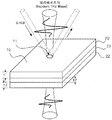
- FIG. 1 is a perspective view showing the basic structure of a terahertz wave modulator according to the present invention.
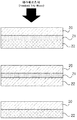
- FIG. 2 is a side view of a structure part manufactured differently to compare and analyze the material structure part, which is a core part of the terahertz wave modulator according to the present invention, and the efficiency and characteristics of the modulator according to the characteristic thereof.
- FIG. 3 is a graph showing transmission characteristics of terahertz waves measured in a modulation device according to an embodiment of the present invention.
- FIG. 4 is a graph showing transmission characteristics of terahertz waves measured in a modulation device according to an embodiment of the present invention.
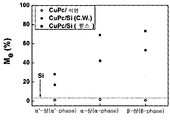
- FIG. 5 is a graph illustrating modulation efficiency of a terahertz wave according to a pick value according to an embodiment of the present invention.
- 6 is a graph showing a change in transmission efficiency when the intensity of incident light is changed continuously.
- FIG. 7 is a conceptual diagram illustrating a principle of terahertz wave waveform modulation.
- FIG. 8 is a perspective view showing one of the representative structures used for the study of similar surface plasmons.
- the terahertz wave modulator includes a semiconductor substrate 22, a terahertz modulation layer including the organic material layer 21 formed on the semiconductor substrate 22, and a first incident wave including the terahertz wave region. And a first incident wave irradiating means for irradiating the terahertz modulation layer perpendicularly to the terahertz modulation layer, wherein the terahertz modulation layer is formed of quartz, sapphire, and PMA on the organic material layer 21. It is characterized in that it further comprises a transparent layer 20 made of a material selected from) and the transparent layer is preferably a quartz layer made of quartz.
- the terahertz wave modulator according to the present invention may further include a second incident wave irradiation means for irradiating a second incident wave which is pulsed light or incident light at an angle adjusted to the terahertz modulation layer.
- Figure 1 is a perspective view showing the basic structure of a terahertz wave modulator according to the present invention.
- the terahertz wave modulator according to the present invention is deposited on a transparent layer 20 having an upper surface 10, a semiconductor substrate 22 having a lower surface (not shown), and deposited on the semiconductor substrate 22.
- the organic material layer 21 disposed between the semiconductor substrates 22 is formed of three independent layers.
- the organic material layer 21 includes all organic materials that allow free holes excited in a semiconductor to be injected through an interface with the organic material layer, but preferably phthalocyanine, anthracene, or tetra Tetracene, pentacene, perylenetetracarboxylic dihydride (PTCDA, 3,4,9,10-perylenetetracarboxylic dianhydride), C60 (C60), aluminum triquinoleate (Alq3, aluminum-tris -quinolate, and rubrene may be an organic material, and more preferably, phthalocyanine copper (CuPc, copper pthalocyanine).
- PTCDA perylenetetracarboxylic dihydride
- Alq3 aluminum triquinoleate
- Alq3 aluminum-tris -quinolate
- rubrene may be an organic material, and more preferably, phthalocyanine copper (CuPc, copper pthalocyanine).
- the semiconductor substrate includes all semiconductors capable of exciting free electrons by incident light while having excellent transmission characteristics in the terahertz wave region.
- the organic material structure on the semiconductor is deposited by thermal evaporation and the transparent layer on the intermediate layer is laminated by adhesive method.
- This transparent layer also serves to prevent the oxidation of organic materials to increase the stability of the device.
- the thickness (h1, h2, h3) of each layer is composed of 100 ⁇ m for the transparent layer as the upper layer, 200 ⁇ m for the organic material layer constituting the middle layer, and 500 ⁇ m for the semiconductor as the lower layer.
- the thickness (h1, h2, h3) of each layer is composed of 100 ⁇ m for the transparent layer as the upper layer, 200 ⁇ m for the organic material layer constituting the middle layer, and 500 ⁇ m for the semiconductor as the lower layer.
- the second incident wave for exciting free electrons / holes has a constant angle of incidence such that the first incident wave in the terahertz wave region is vertically incident on the incident point 11 of the upper surface 10. It is designed to be incident on the incident point 11 of the upper surface 10.
- the second incident wave is in the visible light band and is totally reflected by the semiconductor layer, only the transmitted terahertz wave is finally measured on the lower surface of the opposite side.
- the present invention is characterized in that the first incident wave in the terahertz wave region can block more than 70% when the second incident wave is irradiated to the semiconductor deposited on the surface of the organic material, such a reduction of the transmission of the terahertz wave
- the crystallinity of the organic material deposited on the semiconductor, the intensity of the incident light, and the characteristics of the incident light are manifested in various properties.
- Phthalocyanine copper deposited by a thermal evaporation method on a semiconductor substrate according to an embodiment of the present invention exhibits different crystal properties according to the thermal evaporation method, and exhibits different terahertz wave transmission characteristics according to such crystal properties. That is, at least a part of the organic material layer 21 according to the present invention may be a crystalline beta phase.
- the reduction in the transmission of terahertz waves is 20% or less, whereas the reduction in the transmission of terahertz waves is improved to 70% or more when the heat treatment temperature is increased to 150 and 250 ° C.
- the degree of decrease in the transmission of the terahertz wave differs depending on the characteristics of the incident light.
- the incident light continuous light and pulsed light were used to measure the decrease in the transmission characteristics.
- the pulsed light increased more than 30% more than the continuous light.
- the transmittance of terahertz waves was reduced by 55% for continuous light and 70% for pulsed light at 80 80 incident light.
- FIG. 2 is a side view of a structure part manufactured differently to compare and analyze the material structure part, which is a core part of the terahertz wave modulator according to the present invention, and the efficiency and characteristics of the modulator according to the characteristics thereof.
- the structure of the middle of Figure 2 consists of a transparent layer 20 / organic material 21 / transparent layer 20 in this case it was confirmed that the modulation efficiency of terahertz wave is extremely low, the structure below Figure 2 is a transparent layer 20 / It consists of the semiconductor 22, but also in this case it was confirmed that the modulation efficiency is extremely low.
- a quartz transparent layer in which excitation of free electrons and holes cannot occur in a visible light region used as incident light is used instead of a semiconductor substrate.
- the transmission of terahertz waves with or without strong incident light was less than 1%.
- the difference was less than 1% in all samples manufactured under various heat treatment conditions. This is a result showing that the decrease in the transmission of teraherpa is a contribution by free electrons / holes excited on the semiconductor substrate.
- the measurement was performed using only the semiconductor substrate without the organic material layer, as shown in the following structure of FIG. 2.
- the difference in the transmittance of terahertz waves with and without incident light was within 3%, and the difference was within 1% between samples fabricated differently by heat treatment conditions. This shows that the organic material deposited on the semiconductor is necessary to reduce the transmission of terahertz waves.
- the free holes excited in the semiconductor are injected into the phthalocyanine copper.
- the combined structure of the semiconductor / organic material serves to separate the excited free electrons and holes and thus survives the excited state for a long time to form a layer having a certain degree of effective metallicity to block terahertz waves. do. This is determined by the presence or absence of incident light, thereby enabling ultra-fast terahertz wave transmission modulation using incident light.
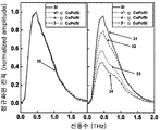
- FIG. 3 is a graph showing transmission characteristics of terahertz waves measured in a modulation device according to an embodiment of the present invention.
- the transmission characteristic of the terahertz wave does not change (30).
- the amorphous alpha phase ( ⁇ '-phase) blocks the transmission of terahertz waves by about 20% (32)
- the crystalline alpha phase ( ⁇ -phase) and crystalline beta-phase (beta-phase) were found to block the transmission of terahertz waves by 45% (33) and 55% (34), respectively.
- the better the crystallinity is developed the better the blocking characteristics of terahertz waves, and thus the terahertz wave modulation efficiency increases.
- FIG. 4 is also a graph showing the transmission characteristics of the terahertz wave measured in the modulation device according to an embodiment of the present invention.
- 3 is a result measured in the same environment as in FIG. 3, and the difference from FIG. 3 is that incident light is measured using pulsed waves instead of continuous light.
- the amorphous alpha phase ( ⁇ '-phase) blocks the transmission of terahertz waves by about 25% (42), and the crystalline alpha phase ( ⁇ -phase)
- the crystalline beta phase ( ⁇ -phase) it was shown to block the transmission of terahertz wave more than 65% (43), 70% (44), respectively. That is, when the pulsed wave (pulsed wave) is used, it can be seen that the modulation efficiency of the terahertz wave more than 30% on average.
- FIG. 5 is a graph showing modulation efficiency of a terahertz wave based on a pick value according to an embodiment of the present invention, and in order to compare modulation efficiency according to structures, modulation efficiency in three structures shown in FIG. 2 is measured. It is shown.
- the transparent layer 20 / semiconductor 22 or the transparent layer 20 / organic material 21 / transparent layer 20 structure shows similar transmission characteristics for organic materials having various crystallinities made under different manufacturing conditions. In the structure of the transparent layer 20 / organic material 21 / semiconductor 22, it can be clearly seen that the modulation efficiency of the terahertz wave is maximized when incident light is present. This is a result showing that the optimized structure of the modulation device is a transparent layer / organic material / semiconductor according to an embodiment of the present invention.
- FIG. 6 is a graph showing a change in transmission efficiency when the incident light is continuous light and the intensity of the incident light is continuously changed.
- Such characteristics can be utilized in a terahertz wave device capable of modulating modulation efficiency that can control the transmission efficiency of terahertz waves when the incident light intensity is changed.
- the present invention is characterized in that the waveform of the terahertz wave in the time domain 70 can be modulated based on the above experimental results (FIGS. 3 to 6).
- the pulsed terahertz waves 71, 72, and 73 form longer waveforms in the time domain than the incident light 77 placed in the visible light region.
- each pulse of incident light can be placed at a specific different location of the terahertz wave using a time delay method.
- Terahertz waves modulated in the time domain can induce variations in the width, amplitude, and phase of the transmission wavelength in the spectrum, thereby providing a wide range of terahertz wave modulation devices.
- the present invention may provide a highly functional terahertz wave modulation device having various characteristics in combination with the properties of the similar surface plasmon or meta material based on the above experimental results (FIGS. 3 to 6).
- Structured organic materials deposited on semiconductors and then incident light on them can generate the properties of similar surface plasmons or metamaterials, which can be combined with the ultrafast modulation capabilities of transparent / organic / semiconductor structures to form terahertz wave devices. Can provide. At this time, in order to apply the properties of the similar surface plasmon or meta-materials, all types of structures or shape patterns known in the art may be applied.
- FIG. 8 is a perspective view showing one of the representative structures used for the study of similar surface plasmons.
- the organic material 80 When the organic material 80 is formed into a pattern 81 having a specific shape on the semiconductor substrate 82, and then incident light is reflected, a layer having metallicity is formed by free electrons / holes excited by the semiconductor substrate and the organic material. Surface plasmon properties appear, which is manifested by transmission resonance at certain wavelengths.
- the present invention is characterized in that the transmission resonance can be adjusted according to the presence or absence of incident light.
- Organic materials deposited on semiconductor substrates can be fabricated in a variety of shapes and structures, enabling a highly functional terahertz wave modulation device with a variety of functions.
Landscapes
- Physics & Mathematics (AREA)
- Chemical & Material Sciences (AREA)
- Nonlinear Science (AREA)
- Engineering & Computer Science (AREA)
- Materials Engineering (AREA)
- Optics & Photonics (AREA)
- General Physics & Mathematics (AREA)
- Spectroscopy & Molecular Physics (AREA)
- Inorganic Chemistry (AREA)
- Electromagnetism (AREA)
- Nanotechnology (AREA)
- Optical Modulation, Optical Deflection, Nonlinear Optics, Optical Demodulation, Optical Logic Elements (AREA)
Abstract
본 발명은 테라헤르츠파 변조장치에 관한 것으로서 반도체 기판, 상기 반도체 기판 위에 형성된 유기물질층을 포함하는 테라헤르츠 변조층 및 테라헤르츠파 영역을 포함하는 제1 입사파를 상기 테라헤르츠 변조층에 수직으로 입사하도록 조사하는 제1 입사파 조사 수단을 포함하는 것을 특징으로 하며, 투과된 테라헤르츠파는 반도체 위에 증착된 유기물질의 결정 정도와 입사하는 입사광의 세기에 의해 다양하게 변하며 이를 이용하여 변조 효율을 극대화시킬 수 있고, 시간 영역상에서의 파형 변형을 통해 파장폭, 진폭, 위상 등을 변조하기 위한 소자를 제공하며, 더 나아가 유사 표면 플라즈몬 또는 메타 물질과 결합하여 고기능성 테라헤르츠파 변조 소자를 가능하게 하여 광학용으로 폭넓게 활용이 가능하다.
Description
본 발명은 테라헤르츠파 변조장치에 관한 것으로서, 더욱 상세하게는 입사광에 의해서 여기된 양공의 주입 및 수송에 의해서 테라헤르츠파 변조가 가능하고, 입사파의 세기 및 유기물질의 결정상태에 따라서 다양한 변조가 가능한 테라헤르츠파 변조장치에 관한 것이다.
다양한 전자기파 영역대에서 투과 파장의 진폭(amplitude), 위상(phase), 편광(polarization)등을 변조하고 조정하기 위한 노력들이 폭넓게 진행되어 왔다.
특히, 전자기파 영역 대에서 새롭게 개척되고 있는 테라헤르츠파는 이를 위한 다양한 방법들이 최근 제시되고 있다. 테라헤르츠파에서 발생하는 유사 표면 플라즈몬 (designer surface plasmon) 공진을 이용한다거나 메타물질(metamaterial)을 이용하는 방법들이 제시되기도 하였고, 반도체 등에서 자유 전자를 여기하는 방법을 통해 테라헤르츠파의 진폭을 조절하는 방법이 제시되기도 하였다.
하지만, 그 변조 효율의 한계성 및 제작의 비효율성으로 인하여 새로운 변조 방법에 대한 필요성이 강하게 제기되고 있는 실정이다.
따라서, 본 발명이 해결하고자 하는 첫 번째 과제는 투과되는 테라헤르츠파를 다양하게 변화시키고, 변조 효율을 극대화시킬 수 있는 테라헤르츠파 변조장치를 제공하는 것이다.
본 발명이 해결하고자 하는 두 번째 과제는 테라헤르츠파의 투과를 변조할 수 있고, 테라헤르츠파 전 파장 영역에서 진폭을 균일하게 변조할 수 있는 테라헤르츠파 스위칭 소자를 제공하는 것이다.
본 발명은 상기 첫 번째 과제를 달성하기 위하여,
(a) (i) 반도체 기판 및 (ii) 상기 반도체 기판 위에 형성된 유기물질층을 포함하는 테라헤르츠 변조층 및 (b) 테라헤르츠파 영역을 포함하는 제1 입사파를 상기 테라헤르츠 변조층에 수직으로 입사하도록 조사하는 제1 입사파 조사 수단을 포함하는 것을 특징으로 하는 헤라테르츠파 변조장치를 제공한다.
본 발명의 일 실시예에 의하면, 상기 유기물질층은 프탈로시아닌 구리(Copper phthalocyanine), 안트라센(anthrancene), 테트라센(tetracene), 펜타센(pentacene), 페릴렌테트라카르복실 다이아하이드라이드(PTCDA, 3,4,9,10 -perylenetetracarboxylic dianhydride), 씨60(C60), 알루미늄 트리퀸올레이트(Alq3, aluminum-tris-quinolate), 및 루브렌(rubrene) 중에서 선택된 유기물질의 층일 수 있다.
본 발명의 일 실시예에 의하면, 상기 유기물질층의 적어도 일부분은 베타상의 결정질일 수 있다.
본 발명의 일 실시예에 의하면, 상기 유기물질층은 100-500 ℃에서 열증착 방식으로 증착될 수 있다.
본 발명의 일 실시예에 의하면, 상기 테라헤르츠 변조층은 (iii) 상기 유기물질층 위에 석영, 사파이어 및 피엠엠에이(PMMA) 중에서 선택된 물질로 구성된 투명층을 추가로 포함할 수 있다.
본 발명의 일 실시예에 의하면, 상기 테라헤르츠 변조장치는 (c) 상기 테라헤르츠 변조층에 조절된 각도로 펄스광 또는 입사광인 제2 입사파를 입사하도록 조사하는 제2 입사파 조사 수단을 추가로 포함할 수 있다.
본 발명의 일 실시예에 의하면, 상기 제2 입사파는 펄스광일 수 있다.
본 발명의 일 실시예에 의하면, 상기 유기물질층에는 일정한 패턴을 가지는 복수 개의 구멍들의 배열을 포함할 수 있고, 상기 구멍은 상기 유기물질층을 관통할 수 있다.
본 발명은 상기 두 번째 과제를 달성하기 위하여,
상기의 테라헤르츠파 변조장치를 포함하고, 상기 제2 입사파의 조사 여부를 결정하는 제2 입사파 조사 조절 수단을 추가로 포함하는 것을 특징으로 하는 테라헤르츠파 스위칭 소자를 제공한다.
본 발명의 테라헤르츠파 변조장치에 의하면, 투과된 테라헤르츠파는 반도체 위에 증착된 유기물질의 결정 정도와 입사하는 입사파의 세기에 의해 다양하게 변하며 이를 이용하여 변조 효율을 극대화시킬 수 있고, 시간 도메인상에서의 파형 변형을 통해 파장폭, 진폭, 위상 등을 변조하기 위한 소자를 제공할 수 잇으며, 더 나아가 유사 표면 플라즈몬 또는 메타 물질과 결합하여 고기능성 테라헤르츠파 변조 소자를 가능하게 하여 광학용으로 폭넓게 활용이 가능하다.
도 1은 본 발명에 따른 테라헤르츠파 변조장치의 기본 구조를 나타내는 사시도이다.
도 2는 본 발명에 따른 테라헤르츠파 변조장치의 핵심 부분인 물질 구조부분과 이의 특징에 따른 변조장치의 효율 및 특성을 비교 분석하기 위하여 다르게 제작한 구조부분의 측면도이다.
도 3은 본 발명의 일 구현예에 따른 변조장치에서 측정된 테라헤르츠파의 투과 특성을 나타내는 그래프이다.
도 4는 본 발명의 일 구현예에 따른 변조장치에서 측정된 테라헤르츠파의 투과 특성을 나타내는 그래프이다.
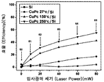
도 5는 본 발명의 일 실시예에 따른 테라헤르츠파의 변조 효율을 픽값을 기준으로 나타낸 그래프이다.
도 6은 입사광의 세기를 연속적으로 바꾸었을 때의 투과 효율의 변화를 나타내는 그래프이다.
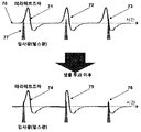
도 7은 테라헤르츠파 파형 변조의 원리를 보여주는 개념도이다.
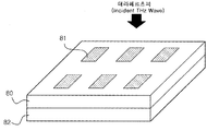
도 8은 유사 표면 플라즈몬의 연구를 위해 사용되는 대표적인 구조중 하나를 보여주는 사시도이다.
이하, 첨부된 도면을 참조하여 본 발명의 실시예를 상세하게 설명한다. 우선, 도면들 중 동일한 구성요소 또는 부품들은 가능한 한 동일한 참조부호를 나타내고 있음에 유의해야 한다. 본 발명을 설명함에 있어서 관련된 공지기능 혹은 구성에 대한 구체적인 설명은 본 발명의 요지를 모호하게 하지 않기 위해 생략한다.
본 발명에 따른 테라헤르츠파 변조장치는 반도체 기판(22), 상기 반도체 기판(22) 위에 형성된 유기물질층(21)을 포함하는 테라헤르츠 변조층 및 테라헤르츠파 영역을 포함하는 제1 입사파를 상기 테라헤르츠 변조층에 수직으로 입사하도록 조사하는 제1 입사파 조사 수단을 포함하는 것을 특징으로 하고, 상기 테라헤르츠 변조층은 상기 유기물질층(21) 위에 석영, 사파이어, 및 피엠엠에이(PMMA) 중에서 선택된 물질로 구성된 투명층(20)을 추가로 포함하는 것을 특징으로 하고 상기 투명층은 석영으로 이루어진 석영층인 것이 바람직하다.
또한, 본 발명에 따른 테라헤르츠파 변조장치는 상기 테라헤르츠 변조층에 조절된 각도로 펄스광 또는 입사광인 제2 입사파를 입사하도록 조사하는 제2 입사파 조사 수단을 추가로 포함할 수 있다.
먼저, 도 1은 본 발명에 따른 테라헤르츠파 변조장치의 기본 구조를 나타내는 사시도이다.
본 발명에 따른 테라헤르츠파 변조기는 상부표면(10)을 갖는 투명층(20), 하부표면(미도시)을 갖는 반도체 기판(22) 그리고, 상기 반도체 기판(22)에 증착되어 투명층(20)과 반도체 기판(22) 사이에 게재되는 유기물질층(21)세 개의 독립된 층으로 형성된다.
상기 유기물질층(21)은 반도체에서 여기된 자유 정공이 유기물질층과의 계면을 통해 주입가능하게 하는 모든 유기 물질을 포함하나, 바람직하게는 프탈로시아닌 구리(Copper phthalocyanine), 안트라센(anthrancene), 테트라센(tetracene), 펜타센(pentacene), 페릴렌테트라카르복실 다이아하이드라이드(PTCDA, 3,4,9,10-perylenetetracarboxylic dianhydride), 씨60(C60), 알루미늄 트리퀸올레이트(Alq3,aluminum-tris-quinolate), 및 루브렌(rubrene) 중에서 선택된 유기물질일 수 있으며, 보다 바람직하게는 프탈로시아닌 구리(CuPc, copper pthalocyanine)일 수 있다.
상기 반도체 기판은 테라헤르츠파 영역에서 투과 특성이 우수하면서 입사광에 의해 자유전자를 여기할 수 있는 모든 반도체를 포함한다.
반도체 위의 유기 물질 구조는 열증착 방식에 의해 증착되고 그 중간층 위의 투명층은 접착 방식에 의해 적층된다. 이러한 투명층은 유기 물질의 산화를 방지하여 장치의 안정성을 높이는 역할도 한다.
기본적으로 각층의 두께(h1, h2, h3)는 상부층인 투명층의 경우 100 ㎛, 중간층을 이루는 유기물질층은 200 ㎛ , 하부층인 반도체의 경우 500 ㎛으로 구성되나, 각 층의 두께는 본 발명에 따른 변조장치의 기능을 최적화하기 위해 다양하게 조절하여 제작될 수 있다.
본 발명에 따른 테라헤르츠파 변조장치에서 테라헤르츠파 영역의 제1 입사파는 상부표면(10)의 입사지점(11) 위로 수직 입사되도록, 자유 전자/정공을 여기하기 위한 제2 입사파는 일정한 입사각을 가지고 상부표면(10)의 입사지점(11) 위로 입사되도록 설계한다.
상기 제2 입사파는 가시광 영역대에 있으므로 반도체층에 의해 전부 반사되므로 최종적으로는 투과된 테라헤르츠파만이 반대면인 하부표면에서 측정된다.
본 발명은 유기물질로 표면이 증착된 반도체에 제2 입사파를 조사하면 테라헤르츠파 영역의 제1 입사파를 70% 이상 차단할 수 있는 것을 특징으로 하고, 이와 같은 테라헤르츠파의 투과 감소 현상은 반도체 위에 증착되는 유기 물질의 결정성, 입사광의 세기 및 입사광의 특성에 의해 다양한 특성으로 나타난다.
본 발명의 일 실시예에 따라 반도체 기판 위에 열증착 방식에 의해 증착된 프탈로시아닌 구리는 열증착 방식에 따라 다른 결정 특성을 보이며, 이러한 결정 특성에 따라 다른 테라헤르츠파 투과 특성을 나타낸다. 즉 본 발명에 따른 상기 유기물질층(21)의 적어도 일부분은 베타상의 결정질일 수 있다.
상온에서 제작한 경우에는 테라헤르츠파의 투과 감소가 20% 이하인 반면 열처리 온도를 150, 250 ℃로 올려서 제작한 경우에는 테라헤르츠파의 투과 감소가 70% 이상으로 향상되는 것을 확인하였다.
열처리 온도가 증가하면 프탈로시아닌 구리의 결정성이 좋아지게 되는데, 150 ℃에서 제작한 경우 좋은 결정성의 알파상(α-phase), 250 ℃에서 제작된 샘플의 경우 좋은 결정성의 베타상(β-phase)을 보여주어 테라헤르츠파의 투과 감소 특성을 보였다.
또한, 입사광의 세기를 점점 증가시키면 테라헤르츠파의 투과 감소도 점점 증가하는 것을 확인하였다. 이러한 특성은 여러 열처리 온도에서 제작한 모든 샘플들에서 그 정도는 다르지만 동일하게 나타난다.
그리고, 테라헤르츠파의 투과 감소 정도는 입사광의 특성에 따라서도 다르게 나타나는 것을 확인하였다. 입사광을 연속광(continuous wave)와 펄스광(pulsed wave)를 사용하여 투과 특성 감소를 측정하였는데 다른 조건이 동일했을 경우 펄스광이 연속광보다 30% 이상 그 효율이 증가하는 것으로 나타났다. 250 ℃에서 제작된 샘플의 경우 80 ㎽의 입사광에서 연속광의 경우는 55%, 펄스광의 경우는 70% 이상 테라헤르츠파의 투과 감소가 나타났다.
하기 도 2는 본 발명에 따른 테라헤르츠파 변조장치의 핵심 부분인 물질 구조부분과 이의 특징에 따른 변조장치의 효율 및 특성을 비교 분석하기 위하여 다르게 제작한 구조부분의 측면도이다.
도 2 중간의 구조는 투명층(20)/유기물질(21)/투명층(20)으로 이루어져 있는데 이 경우 테라헤르츠파의 변조 효율이 극히 낮은 것을 확인하였으며, 도 2 아래의 구조는 투명층(20)/반도체(22)로 이루어져 있는데 이 경우에도 변조 효율이 극히 낮은 것을 확인하였다.
먼저, 하기 도 2의 중간 구조에서와 같이, 입사광으로 사용하는 가시광 영역대에서 자유전자 및 정공의 여기가 일어날 수 없는 석영 투명층을 반도체 기판대신에 사용하였다. 이 경우 강한 입사광이 있는 경우와 없는 경우 테라헤르츠파의 투과는 1% 이하의 차이를 보였다. 여러 열처리 조건에서 제작된 모든 샘플들에서도 그 차이가 1% 이하로 나타났다. 이는 테라헤르파의 투과 감소가 반도체 기판 위에서 여기된 자유 전자/정공에 의한 기여임을 보여주는 결과이다.
또한, 반도체 기판위에 증착된 유기 물질의 기여를 측정하기 위하여 하기 도 2의 아래 구조와 같이, 유기물질층이 없이 반도체 기판만을 가지고 측정을 진행하였다. 이 경우 입사광이 있는 경우와 없는 경우의 테라헤르츠파의 투과도 차이는 3% 이내였고 열처리 조건에 의해 다르게 제작된 샘플들 사이에서는 그 차이가 1% 이내로 나타났다. 이는 테라헤르츠파의 투과 감소를 위해서는 반드시 반도체 위에 증착된 유기 물질이 필요함을 보여주는 것으로 더 나아가 반도체에서 여기된 자유 정공이 프탈로시아닌 구리로 주입되면서 나타나는 현상이다.
이와 같이 반도체/유기 물질이 결합된 구조는 여기된 자유 전자와 정공을 분리시키는 역할을 하여 오랫동안 여기된 상태로 살아남아 일정 정도 이상의 유효한 금속성을 가지는 층을 형성하게 하여 테라헤르츠파를 차단하는 역할을 하게 한다. 이는 입사광의 유무에 의해 결정되므로 입사광을 이용한 초고속 테라헤르츠파 투과 변조를 가능하게 한다.
하기 도 3은 본 발명의 일 구현예에 따른 변조장치에서 측정된 테라헤르츠파의 투과 특성을 나타내는 그래프이다.
제2 입사파로 연속광(continuous wave)을 사용하여 측정하였으며, 입사광이 없는 경우에는 테라헤르츠파의 투과 특성은 변하지 않는 것(30)을 확인할 수 있다. 입사광은 있으나, 유기물질층이 없는 경우(31)와 비교했을 때 비결정성의 알파상(α'-phase)의 경우는 20% 정도 테라헤르츠파의 투과를 차단하고(32), 결정성의 알파상(α-phase)과 결정성의 베타상(β-phase)의 경우는 각각 45%(33), 55%(34) 이상 테라헤르츠파의 투과를 차단하는 것으로 나타났다. 즉, 결정성이 잘 발달할수록 테라헤르츠파를 차단하는 특성이 좋아져 테라헤르츠파 변조 효율이 증가하는 것을 확인할 수 있다.
하기 도 4 역시 본 발명의 일 구현예에 따른 변조장치에서 측정된 테라헤르츠파의 투과 특성을 나타내는 그래프이다. 하기 도 3에서와 동일한 환경에서 측정한 결과이며, 하기 도 3에서와의 차이점은 입사광을 연속광이 아니라 펄스광(pulsed wave)을 사용하여 측정하였다.
이 경우에도 도 3의 경우와 마찬가지로 입사광이 없는 경우 여러 열처리 조건에서 만들어진 모든 구조들에서 테라헤르츠파의 투과 특성이 전혀 변하지 않는 것(40)을 확인할 수 있다. 또한, 입사광이 있는 경우도 다른 열처리 조건과 결정성에 따른 투과 특성의 차이가 도 3에서 나타난 경우와 유사하게 나타나는 것을 확인할 수 있다. 하지만 테라헤르츠파의 변조 효율은 크게 향상되는 것을 확인할 수 있다. 유기물질이 없는 경우(41)와 비교했을 때 비결정성의 알파상(α'-phase)의 경우는 25% 정도 테라헤르츠파의 투과를 차단하고(42), 결정성의 알파상(α-phase)과 결정성의 베타상(β-phase)의 경우는 각각 65%(43), 70%(44) 이상 테라헤르츠파의 투과를 차단하는 것으로 나타났다. 즉, 펄스광(pulsed wave)을 사용했을때에 평균적으로 30% 이상 테라헤르츠파의 변조 효율이 향상된 것을 알 수 있다.
하기 도 5는 본 발명의 일 실시예에 따른 테라헤르츠파의 변조 효율을 픽값을 기준으로 나타낸 그래프이고, 구조에 따른 변조효율을 비교하기 위하여 하기 도 2에 나타난 세 가지 구조에서의 변조 효율을 측정하여 나타내었다. 투명층(20)/반도체(22)나 투명층(20)/유기물질(21)/투명층(20) 구조의 경우는 다른 제작 조건에서 만들어진 다양한 결정성을 가지는 유기물질에 대해서 비슷한 투과 특성을 보여주지만, 투명층(20)/유기물질(21)/반도체(22) 구조에서는 입사광이 존재하는 경우에 테라헤르츠파의 변조 효율이 극대화된다는 것을 명확히 알 수 있다. 이는 변조장치의 최적화된 구조가 본 발명의 일 구현예에 따른 투명층/유기물질/반도체임을 보여주는 결과라 할 수 있다.
하기 도 6은 입사광을 연속광으로하고, 입사광의 세기를 연속적으로 바꾸었을 때의 투과 효율의 변화를 나타내는 그래프이다.
입사광의 세기를 0에서부터 서서히 증가시킴에 따라 투과 효율이 0%에서부터 연속적으로(60→61→62→63→64→65) 증가하는 것을 확인할 수 있다. 이는 입사광에 의해 여기되어 유기 물질쪽으로 주입되는 자유 정공의 수가 입사광의 세기와 함께 증가한다는 것을 보여주는 것이다.
이와 같은 특성은 입사광의 세기를 변화시키게 되면 테라헤르츠파의 투과 효율을 조절할 수 있는 변조 효율 조절 가능한 테라헤르츠파용 소자에 활용될 수 있다.
본 발명은 상기의 실험 결과들(하기 도 3 내지 도 6)을 기반으로 시간 영역상(70)에서의 테라헤르츠파의 파형을 변조할 수 있는 것을 특징으로 한다.
하기 도 7은 테라헤르츠파 파형 변조의 원리를 보여주는 개념도이다. 펄스형 테라헤르츠파(71, 72, 73)는 가시광 영역대에 놓여있는 입사광(77)에 비하여 시간 영역상에서 긴 파형을 형성한다. 그래서 입사광의 각각의 펄스를 시간 지연 방법을 이용하여 테라헤르츠파의 특정한 각기 다른 위치에 놓이게 할 수 있다.
입사광에 따라서 테라헤르츠파의 투과가 감소하는 특성을 이용하면 시간 영역상에서 테라헤르츠파의 파형의 일부분만을 투과시키고 일부분은 선택적으로 차단(74, 75, 76)할 수 있는 장치를 구성할 수 있다. 시간 영역상에서 변조된 테라헤르츠파는 최종적으로 스펙트럼상에서 투과 파장의 폭, 진폭, 위상들의 변화를 유도할 수 있기 때문에 광범위한 기능의 테라헤르츠파 변조 소자를 제공할 수 있다.
또한, 본 발명은 상기의 실험 결과들(하기 도 3 내지 도 6)을 기반으로 유사 표면 플라즈몬 또는 메타 물질의 특성과 결합하여 다양한 특성의 고기능성 테라헤르츠파 변조 소자를 제공할 수 있다.
반도체 위에 증착되는 유기 물질을 구조화한 뒤 그 위에 입사광을 비추면 유사 표면 플라즈몬이나 메타 물질의 특성을 발생시킬 수 있고 이를 투명층/유기물질/반도체 구조가 가지는 초고속 변조 기능과 결합하여 테라헤르츠파용 소자를 제공할 수 있다. 이때 유사 표면 플라즈몬이나 메타 물질의 특성을 적용하기 위하여 종래에 알려져있는 모든 형태의 구조나 형태 패턴을 적용해 볼 수 있다.
하기 도 8은 유사 표면 플라즈몬의 연구를 위해 사용되는 대표적인 구조중 하나를 보여주는 사시도이다.
반도체 기판(82)위에 유기물질(80)을 특정 형태를 가지는 패턴(81)으로 만든 후 입사광을 비추게 되면 반도체 기판과 유기물질에 여기된 자유 전자/정공에 의해 금속성을 가지는 층이 형성되어 유사 표면 플라즈몬 특성이 나타나게 되는데 이는 특정 파장에서의 투과 공진 현상으로 나타난다.
본 발명은 투과 공진을 입사광의 유무에 따라 조절할 수 있는 것을 특징으로 한다. 반도체 기판위에 증착되는 유기물질은 다양한 형태와 구조로 제작 가능하기 때문에 다양한 기능의 고기능성 테라헤르츠파 변조 소자를 가능하게 한다.
이상과 같이 본 발명에 따른 과 이에 따른 실시예를 예시한 도면을 참조로 하여 설명하였으나, 이는 본 발명을 보다 구체적으로 설명하기 위한 것으로, 본 명세서에 개시된 실시예와 도면에 의해 본 발명이 한정되는 것은 아니며, 본 발명의 기술사상 범위 내에서 당업자에 의해 다양한 변형이 이루어질 수 있다.
Claims (9)
- (a) (i) 반도체 기판 및 (ii) 상기 반도체 기판 위에 형성된 유기물질층을 포함하는 테라헤르츠 변조층 및(b) 테라헤르츠파 영역을 포함하는 제1 입사파를 상기 테라헤르츠 변조층에 수직으로 입사하도록 조사하는 제1 입사파 조사 수단을 포함하는 것을 특징으로 하는 테라헤르츠파 변조장치.
- 제 1 항에 있어서,상기 유기물질층은 프탈로시아닌 구리(Copper phthalocyanine), 안트라센(anthrancene), 테트라센(tetracene), 펜타센(pentacene), 페릴렌테트라카르복실 다이아하이드라이드(PTCDA, 3,4,9,10-perylenetetracarboxylic dianhydride), 씨60(C60), 알루미늄 트리퀸올레이트(Alq3,aluminum-tris-quinolate), 및 루브렌(rubrene) 중에서 선택된 유기물질의 층인 것을 특징으로 하는 테라헤르츠파 변조장치.
- 제 1 항에 있어서,상기 유기물질층의 적어도 일부분은 베타상의 결정질인 것을 특징으로 하는 테라헤르츠파 변조장치.
- 제 1 항에 있어서,상기 유기물질층은 100-500 ℃에서 열증착 방식으로 증착된 것을 특징으로 하는 테라헤르츠파 변조장치.
- 제 1 항에 있어서,상기 테라헤르츠 변조층은 (iii) 상기 유기물질층 위에 석영, 사파이어, 및 피엠엠에이(PMMA) 중에서 선택된 물질로 구성된 투명층을 추가로 포함하는 것을 특징으로 하는 테라헤르츠파 변조장치.
- 제 5 항에 있어서,상기 테라헤르츠 변조장치는 (c) 상기 테라헤르츠 변조층에 조절된 각도로 펄스광 또는 입사광인 제2 입사파를 입사하도록 조사하는 제2 입사파 조사 수단을 추가로 포함하는 것을 특징으로 하는 테라헤르츠파 변조장치.
- 제 6 항에 있어서,상기 제2 입사파는 펄스광인 것을 특징으로 하는 테라헤르츠파 변조장치.
- 제 1 항에 있어서,상기 유기물질층에는 일정한 패턴을 가지는 복수 개의 구멍들의 배열을 포함하고, 상기 구멍은 상기 유기물질층을 관통하는 것을 특징으로 하는 테라헤르츠파 변조장치.
- 제 6 항 또는 제 7 항에 따른 테라헤르츠파 변조장치를 포함하고, 상기 제2 입사파의 조사 여부를 결정하는 제2 입사파 조사 조절 수단을 추가로 포함하는 것을 특징으로 하는 테라헤르츠파 스위칭 소자.
Priority Applications (1)
| Application Number | Priority Date | Filing Date | Title |
|---|---|---|---|
| US14/005,401 US9231226B2 (en) | 2011-03-16 | 2011-12-12 | Terahertz wave modulator based on hole-injection and -transfer |
Applications Claiming Priority (2)
| Application Number | Priority Date | Filing Date | Title |
|---|---|---|---|
| KR1020110023167A KR101175699B1 (ko) | 2011-03-16 | 2011-03-16 | 정공 주입 및 수송에 기반한 테라헤르츠파 변조장치 |
| KR10-2011-0023167 | 2011-03-16 |
Publications (1)
| Publication Number | Publication Date |
|---|---|
| WO2012124883A1 true WO2012124883A1 (ko) | 2012-09-20 |
Family
ID=46830921
Family Applications (1)
| Application Number | Title | Priority Date | Filing Date |
|---|---|---|---|
| PCT/KR2011/009551 Ceased WO2012124883A1 (ko) | 2011-03-16 | 2011-12-12 | 양공 주입 및 수송에 기반한 테라헤르츠파 변조장치 |
Country Status (3)
| Country | Link |
|---|---|
| US (1) | US9231226B2 (ko) |
| KR (1) | KR101175699B1 (ko) |
| WO (1) | WO2012124883A1 (ko) |
Cited By (2)
| Publication number | Priority date | Publication date | Assignee | Title |
|---|---|---|---|---|
| CN102902130A (zh) * | 2012-09-27 | 2013-01-30 | 中国计量学院 | 高速太赫兹波调制装置及其方法 |
| CN108683408A (zh) * | 2018-04-13 | 2018-10-19 | 东南大学 | 谐波幅相可独立调控的时域编码超表面 |
Families Citing this family (13)
| Publication number | Priority date | Publication date | Assignee | Title |
|---|---|---|---|---|
| KR101296323B1 (ko) | 2012-08-28 | 2013-08-13 | 광주과학기술원 | 전자파 흡수체 및 그 제조 방법 |
| KR101805881B1 (ko) * | 2016-02-01 | 2017-12-07 | 연세대학교 산학협력단 | 위상절연체를 이용한 테라헤르츠 펄스 변조 장치 및 방법 |
| CN105572797B (zh) * | 2016-02-15 | 2021-02-26 | 欧阳征标 | 一种太赫兹波脉冲调幅信号与光脉冲调幅信号变换放大器 |
| EP3658985A4 (en) | 2017-07-24 | 2021-05-19 | Terahertz Group Ltd. | High frequency optical switch and fabrication methods thereof |
| CN108983411B (zh) * | 2018-07-23 | 2020-07-07 | 郑州大学 | 一种磁场调控太赫兹波调制器及其制作方法 |
| CN113050305B (zh) * | 2021-03-03 | 2023-03-24 | 北京航空航天大学 | 一种基于MoS2和Si复合结构的太赫兹调制器及其调控方法 |
| CN113075791B (zh) * | 2021-03-22 | 2022-03-29 | 华中科技大学 | 一种基于静电驱动纯硅基光栅的太赫兹调制器及制备方法 |
| FR3122741A1 (fr) | 2021-05-04 | 2022-11-11 | Eduardo Antonio ALVEAR CABEZON | Procédé et dispositif d’analyse de modulation térahertz à cadence rapide, profonde et large bande |
| CN113267913B (zh) * | 2021-05-29 | 2022-10-04 | 枣庄学院 | 一种超材料调制器 |
| TWI803954B (zh) | 2021-08-27 | 2023-06-01 | 國立清華大學 | 太赫茲光調制器及太赫茲空間光調制器 |
| CN114740615B (zh) * | 2022-04-11 | 2023-06-30 | 南京邮电大学 | 一种可调太赫兹衰减器及其制备方法 |
| CN116203739B (zh) * | 2023-01-13 | 2024-11-15 | 首都师范大学 | 基于二维碲薄膜的光控太赫兹波调制芯片及其制备方法 |
| CN119667975B (zh) * | 2025-01-16 | 2026-04-07 | 桂林电子科技大学 | 一种光控超高q值的太赫兹超表面调制器 |
Citations (4)
| Publication number | Priority date | Publication date | Assignee | Title |
|---|---|---|---|---|
| JPH10333192A (ja) * | 1997-05-30 | 1998-12-18 | Hitachi Ltd | 有機無機複合超格子型光変調器 |
| JP2007300022A (ja) * | 2006-05-02 | 2007-11-15 | Material Design Factory:Kk | テラヘルツ波増幅装置、テラヘルツ波変調装置ならびにこれを用いた通信装置およびセンシング装置 |
| JP2009282073A (ja) * | 2008-05-19 | 2009-12-03 | Tohoku Univ | テラヘルツ波の強度変調方法およびテラヘルツ波の強度変調装置 |
| WO2010006611A1 (en) * | 2008-07-15 | 2010-01-21 | Danmarks Tekniske Universitet | All-optical control of thz radiation in parallel plate waveguides |
Family Cites Families (3)
| Publication number | Priority date | Publication date | Assignee | Title |
|---|---|---|---|---|
| JP4972728B2 (ja) * | 2005-08-30 | 2012-07-11 | 日本電信電話株式会社 | 有機材料層形成方法 |
| JP4785194B2 (ja) * | 2006-08-25 | 2011-10-05 | 日本碍子株式会社 | スラブ型2次元フォトニック結晶構造の製造方法 |
| WO2008121159A2 (en) * | 2006-10-19 | 2008-10-09 | Los Alamos National Security Llc | Active terahertz metamaterial devices |
-
2011
- 2011-03-16 KR KR1020110023167A patent/KR101175699B1/ko not_active Expired - Fee Related
- 2011-12-12 US US14/005,401 patent/US9231226B2/en not_active Expired - Fee Related
- 2011-12-12 WO PCT/KR2011/009551 patent/WO2012124883A1/ko not_active Ceased
Patent Citations (4)
| Publication number | Priority date | Publication date | Assignee | Title |
|---|---|---|---|---|
| JPH10333192A (ja) * | 1997-05-30 | 1998-12-18 | Hitachi Ltd | 有機無機複合超格子型光変調器 |
| JP2007300022A (ja) * | 2006-05-02 | 2007-11-15 | Material Design Factory:Kk | テラヘルツ波増幅装置、テラヘルツ波変調装置ならびにこれを用いた通信装置およびセンシング装置 |
| JP2009282073A (ja) * | 2008-05-19 | 2009-12-03 | Tohoku Univ | テラヘルツ波の強度変調方法およびテラヘルツ波の強度変調装置 |
| WO2010006611A1 (en) * | 2008-07-15 | 2010-01-21 | Danmarks Tekniske Universitet | All-optical control of thz radiation in parallel plate waveguides |
Cited By (3)
| Publication number | Priority date | Publication date | Assignee | Title |
|---|---|---|---|---|
| CN102902130A (zh) * | 2012-09-27 | 2013-01-30 | 中国计量学院 | 高速太赫兹波调制装置及其方法 |
| CN108683408A (zh) * | 2018-04-13 | 2018-10-19 | 东南大学 | 谐波幅相可独立调控的时域编码超表面 |
| CN108683408B (zh) * | 2018-04-13 | 2021-05-11 | 东南大学 | 谐波幅相可独立调控的时域编码超表面 |
Also Published As
| Publication number | Publication date |
|---|---|
| KR101175699B1 (ko) | 2012-08-21 |
| US9231226B2 (en) | 2016-01-05 |
| US20140001379A1 (en) | 2014-01-02 |
Similar Documents
| Publication | Publication Date | Title |
|---|---|---|
| WO2012124883A1 (ko) | 양공 주입 및 수송에 기반한 테라헤르츠파 변조장치 | |
| Lai et al. | High‐performance flexible self‐powered photodetectors utilizing spontaneous electron and hole separation in quasi‐2D halide perovskites | |
| Lin et al. | Enhancement and suppression of thermal emission by a three-dimensional photonic crystal | |
| Cocoyer et al. | Implementation of submicrometric periodic surface structures toward improvement of organic-solar-cell performances | |
| US7898176B2 (en) | Fluidic thermal management article and method | |
| CN1278157C (zh) | 折射率可调的薄膜干涉涂层 | |
| Niko et al. | Optical absorbance of oriented thin films | |
| US10088604B2 (en) | Transparent substrate for optical elements, polarizer plate for liquid crystal display device using said substrate, and organic electroluminescence element | |
| US7742673B2 (en) | Thermal mangement article having thermal wave guide | |
| CN105811120B (zh) | 基于光驱动连续可调的可降解太赫兹超材料及其制备方法 | |
| Chein Sheng Ly et al. | Visible‐to‐MIR broadband modulating electrochromic metal oxides‐based coating for thermal management | |
| Sedeh et al. | Active multiple access secure communication enabled by graphene-based time-modulated metasurfaces | |
| KR20150052216A (ko) | 유기 일렉트로 루미네선스 소자 및 전자 기기 | |
| Ding et al. | Intrinsic polarization and tunable color of electroluminescence from organic single crystal-based light-emitting devices | |
| KR102730614B1 (ko) | 광소자 및 그의 제조방법 | |
| US20090097798A1 (en) | Plasmonic high-speed devices for enhancing the performance of microelectronic devices | |
| Amin et al. | Polarization-state modulation in fano resonant graphene metasurface reflector | |
| Zhang et al. | Organic Single‐Crystalline Microwire Arrays toward High‐Performance Flexible Near‐Infrared Phototransistors | |
| CN115911885B (zh) | 基于温控网状二氧化钒微结构的太赫兹宽带吸波器 | |
| Long et al. | Active terahertz nonlocal metasurfaces with liquid crystal elastomers | |
| Zhu et al. | Tristate switching of terahertz metasurfaces enabled by transferable VO2 | |
| Rao et al. | Transparent, flexible MAPbI 3 perovskite microwire arrays passivated with ultra-hydrophobic supramolecular self-assembly for stable and high-performance photodetectors | |
| Yoshino et al. | Organic electronic devices based on polymeric material and tunable photonic crystal | |
| KR20140118534A (ko) | 도너기판 및 이를 이용한 전사패턴 형성방법 | |
| Torii et al. | Organic nanowire lasers with epitaxially grown crystals of semiconducting oligomers |
Legal Events
| Date | Code | Title | Description |
|---|---|---|---|
| 121 | Ep: the epo has been informed by wipo that ep was designated in this application |
Ref document number: 11861182 Country of ref document: EP Kind code of ref document: A1 |
|
| NENP | Non-entry into the national phase |
Ref country code: DE |
|
| WWE | Wipo information: entry into national phase |
Ref document number: 14005401 Country of ref document: US |
|
| 122 | Ep: pct application non-entry in european phase |
Ref document number: 11861182 Country of ref document: EP Kind code of ref document: A1 |