WO2012124510A1 - スナバコンデンサの充電方法 - Google Patents
スナバコンデンサの充電方法 Download PDFInfo
- Publication number
- WO2012124510A1 WO2012124510A1 PCT/JP2012/055363 JP2012055363W WO2012124510A1 WO 2012124510 A1 WO2012124510 A1 WO 2012124510A1 JP 2012055363 W JP2012055363 W JP 2012055363W WO 2012124510 A1 WO2012124510 A1 WO 2012124510A1
- Authority
- WO
- WIPO (PCT)
- Prior art keywords
- snubber capacitor
- phase
- charging
- snubber
- voltage
- Prior art date
- Legal status (The legal status is an assumption and is not a legal conclusion. Google has not performed a legal analysis and makes no representation as to the accuracy of the status listed.)
- Ceased
Links
Images


Classifications
-
- H—ELECTRICITY
- H02—GENERATION; CONVERSION OR DISTRIBUTION OF ELECTRIC POWER
- H02M—APPARATUS FOR CONVERSION BETWEEN AC AND AC, BETWEEN AC AND DC, OR BETWEEN DC AND DC, AND FOR USE WITH MAINS OR SIMILAR POWER SUPPLY SYSTEMS; CONVERSION OF DC OR AC INPUT POWER INTO SURGE OUTPUT POWER; CONTROL OR REGULATION THEREOF
- H02M1/00—Details of apparatus for conversion
- H02M1/32—Means for protecting converters other than automatic disconnection
- H02M1/34—Snubber circuits
-
- H—ELECTRICITY
- H02—GENERATION; CONVERSION OR DISTRIBUTION OF ELECTRIC POWER
- H02M—APPARATUS FOR CONVERSION BETWEEN AC AND AC, BETWEEN AC AND DC, OR BETWEEN DC AND DC, AND FOR USE WITH MAINS OR SIMILAR POWER SUPPLY SYSTEMS; CONVERSION OF DC OR AC INPUT POWER INTO SURGE OUTPUT POWER; CONTROL OR REGULATION THEREOF
- H02M5/00—Conversion of AC power input into AC power output, e.g. for change of voltage, for change of frequency, for change of number of phases
- H02M5/40—Conversion of AC power input into AC power output, e.g. for change of voltage, for change of frequency, for change of number of phases with intermediate conversion into DC
- H02M5/42—Conversion of AC power input into AC power output, e.g. for change of voltage, for change of frequency, for change of number of phases with intermediate conversion into DC by static converters
- H02M5/44—Conversion of AC power input into AC power output, e.g. for change of voltage, for change of frequency, for change of number of phases with intermediate conversion into DC by static converters using discharge tubes or semiconductor devices to convert the intermediate DC into AC
- H02M5/453—Conversion of AC power input into AC power output, e.g. for change of voltage, for change of frequency, for change of number of phases with intermediate conversion into DC by static converters using discharge tubes or semiconductor devices to convert the intermediate DC into AC using devices of a triode or transistor type requiring continuous application of a control signal
- H02M5/458—Conversion of AC power input into AC power output, e.g. for change of voltage, for change of frequency, for change of number of phases with intermediate conversion into DC by static converters using discharge tubes or semiconductor devices to convert the intermediate DC into AC using devices of a triode or transistor type requiring continuous application of a control signal using semiconductor devices only
- H02M5/4585—Conversion of AC power input into AC power output, e.g. for change of voltage, for change of frequency, for change of number of phases with intermediate conversion into DC by static converters using discharge tubes or semiconductor devices to convert the intermediate DC into AC using devices of a triode or transistor type requiring continuous application of a control signal using semiconductor devices only having a rectifier with controlled elements
-
- H—ELECTRICITY
- H02—GENERATION; CONVERSION OR DISTRIBUTION OF ELECTRIC POWER
- H02M—APPARATUS FOR CONVERSION BETWEEN AC AND AC, BETWEEN AC AND DC, OR BETWEEN DC AND DC, AND FOR USE WITH MAINS OR SIMILAR POWER SUPPLY SYSTEMS; CONVERSION OF DC OR AC INPUT POWER INTO SURGE OUTPUT POWER; CONTROL OR REGULATION THEREOF
- H02M1/00—Details of apparatus for conversion
- H02M1/32—Means for protecting converters other than automatic disconnection
- H02M1/34—Snubber circuits
- H02M1/348—Passive dissipative snubbers
Definitions
- the present invention relates to a method for charging a snubber capacitor provided for overvoltage protection in a semiconductor switching circuit.
- Snubber capacitors are used for overvoltage protection.
- One of the causes of the overvoltage is, for example, an inrush current that flows when the power is turned on.
- the inrush current is limited by a resistor.
- the inrush current can be limited.
- the current is limited by a resistor, the charging time for completely charging the inrush current to the snubber capacitor becomes long. The switching circuit cannot start switching until this charging is completed.
- An object of the present invention is to provide a method of charging a snubber capacitor that can shorten the charging time of the inrush current.
- a potential difference between both ends of a snubber capacitor connected between buses of a switching circuit that switches the three-phase AC power supply is detected when the three-phase AC power supply is turned on. Based on the detection result, two phases having the same potential difference as the potential difference of the snubber capacitor are determined from the phase voltages of the three-phase AC power supply. The phase in which the voltage increases among the two phases is connected to the positive electrode of the snubber capacitor via the switching circuit, and the phase in which the voltage decreases in the two phases is connected to the negative electrode of the snubber capacitor. Connect through.
- the switching circuit for example, a combination of a converter that rectifies a three-phase alternating current power supply and an inverter that converts the rectified direct current into a three-phase alternating current power supply having a desired frequency and voltage can be used.
- the snubber capacitor is provided on the output side of the converter.
- an indirect matrix converter that converts the voltage and frequency of the three-phase AC power supply can be used.
- the snubber capacitor is connected between the converter unit and the inverter unit of the indirect matrix converter.
- These switching circuits can use a semiconductor switching element having a self-extinguishing capability, for example, a bridge circuit made of a bipolar transistor, MOSFET or IGFET.
- the snubber capacitor is connected between the two-phase voltages having the same potential difference between the both ends of the snubber capacitor, almost no overcurrent flows. Moreover, since the three-phase AC power supply is connected to the snubber capacitor without using a resistor, the snubber capacitor can be charged in a short time.
- a method for charging a snubber capacitor In a switching circuit for switching a three-phase AC power source, when the three-phase AC power source is turned on, the voltage is the same among the phase voltages of the three-phase AC power source. Determine the two phases. The phase in which the voltage rises among the two phases is connected to the positive electrode of the snubber capacitor in the switching circuit via the switching circuit, and the phase in which the voltage drops in the two phases is connected to the negative electrode of the snubber capacitor Are connected via the switching circuit.
- a converter or a converter part of a matrix converter can be used in the same manner as in the above aspect, and a bipolar transistor, MOSFET, or IGFET can be used as the switching element in the switching circuit as in the above aspect. it can.
- a charging completion determination step for determining that the snubber capacitor has been charged may be provided.
- a charging time is calculated from the frequency of the three-phase AC power supply and the potential difference before the snubber capacitor is charged, and it is determined that the charging time has elapsed.
- the next step for example, switching by the switching circuit can be started.
- the charging completion determination step it may be determined that the potential difference of the snubber capacitor has become a predetermined value or more.
- the transition to the next step can be made after the potential difference of the snubber capacitor becomes equal to or greater than a predetermined value to such an extent that an excessive inrush current does not flow. Therefore, this transition can be performed at an early stage.
- the charging completion determination step it is also possible to use one that determines that the remaining phase of the three-phase AC power supply has become zero volts. With this configuration, when the voltage of the remaining phase is zero volts, the two phases connected to both ends of the snubber capacitor have the maximum potential difference, so that the snubber capacitor can be sufficiently charged.
- the filling step of the snubber capacitor can be omitted. That is, the filling of the snubber capacitor is performed when the potential difference between both ends of the snubber capacitor is less than a predetermined value.
- the charging step can be omitted, and the transition to the next step can be performed quickly.
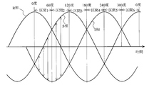
- FIG. 3 is a waveform diagram of each part of the matrix converter of FIG. 2.
- the charging method of the snubber capacitor according to one embodiment of the present invention is performed in an indirect matrix converter 1 as shown in FIG.
- This indirect matrix converter includes a converter 2, a positive side DC intermediate link 4 p, a negative side DC intermediate link 4 n, and an inverter 6.
- the converter 2 has upper bidirectional switch circuits 8ur, 8us, 8ut as upper arms, and lower bidirectional switch circuits 8dr, 8ds, 8dt as lower arms.
- the upper bidirectional switch circuit 8ur and the lower bidirectional switch circuit 8dr are connected in series
- the upper bidirectional switch circuit 8us and the lower bidirectional switch circuit 8ds are connected in series
- the upper bidirectional switch circuit 8ut and the lower Side bidirectional switch circuit 8dt is connected in series. These three series circuits are connected in parallel to each other.
- Both the upper and lower bidirectional switch circuits 8ur and 8dr have unidirectional switch elements such as IGBTs 10a and 10b.
- the IGBT 10a of the upper bidirectional switch circuit 8ur is connected to the positive direct current intermediate link 4p.
- the IGBT 10b of the upper bidirectional switch circuit 8ur is connected to the collector of the IGBT 10a of the lower bidirectional switch circuit 8dr.
- the IGBT 10b of the lower bidirectional switch circuit 8d is connected to the negative DC intermediate link 4n.
- the other upper bidirectional switch circuits 8us and 8ut and the lower bidirectional switch circuits 8ds and 8dt are similarly configured.
- the R-phase power supply of the three-phase AC power supply 13 is connected to the connection point Rin between the upper bidirectional switch circuit 8ur and the lower bidirectional switch circuit 8dr via the DC reactor 15R, and the upper bidirectional switch circuit 8us and the lower side
- the S-phase power supply of the three-phase AC power supply 13 is connected to the connection point Sin with the bidirectional switch circuit 8ds via the DC reactor 15S, and the connection point between the upper bidirectional switch circuit 8ut and the lower bidirectional switch circuit 8dt.
- the T-phase power source of the three-phase AC power source 13 is connected to the Tin via a DC reactor 15T.
- a capacitor 14rs is connected between the connection points Rin and Sin, a capacitor 14st is connected between the connection points Sin and Tin, and a capacitor 14tr is connected between the connection points Tin and Rin.
- These capacitors 14rs, 14st, and 14tr and the DC reactors 15R, 15S, and 15T constitute an input filter.
- the inverter 6 has unidirectional switch elements such as IGBTs 16uu, 16uv and 16uw as upper arms, and unidirectional switch elements such as IGBTs 16du, 16dv and 16dw as lower arms.
- the collector of the IGBT 16uu is connected to the positive direct current intermediate link 4p.
- the emitter of the IGBT 16uu is connected to the collector of the IGBT 16du.
- the emitter of the IGBT 16du is connected to the negative direct current intermediate link 4n. That is, a series circuit of IGBTs 16uu and 16du is connected between the intermediate DC links 4p and 4n.
- Other IGBTs 16uv, 16uw, 16dv, and 16dw are similarly connected.
- a diode 18u is connected in antiparallel between the collectors and emitters of the IGBTs 16uu, 16uv, and 16uw.
- a diode 18d is connected in antiparallel between the collectors and emitters of the IGBTs 16du, 16dv, and 16dw.
- a load for example, an electric actuator 19 is connected to a connection point u to the IGBTs 16 uu and 16 du, a connection point v to the IGBTs 16 uv and 16 dv, and a connection point w to the IGBTs 16 uw and 16 dw.
- a discharge prevention snubber circuit 20u is connected to each IGBT 16uu, 16uv, 16uw.
- a discharge prevention snubber circuit 20d is connected to each IGBT 16du, 16dv, 16dw.
- a series circuit of a snubber capacitor 22u and a snubber diode 24u is connected in parallel between the collectors and emitters of the IGBTs 16uu, 16uv, and 16uw.
- each snubber capacitor 22u is connected to the collectors of the IGBTs 16uu, 16uv, 16uw, and the other end of each snubber capacitor 22u is connected to the anode of each snubber diode 24u.
- the cathode of each snubber diode 24u is connected to the emitters of the IGBTs 16uu, 16uv, and 16uw.
- each snubber discharge resistor 26u is connected to a connection point between each snubber capacitor 22u and each snubber diode 24u, and the other end is connected to a connection point between a snubber capacitor 30 and an anode of a diode 28d described later.
- a series circuit of a snubber capacitor 22d and a snubber diode 24d is connected in parallel between the collectors and emitters of the IGBTs 16du, 16dv, and 16dw.
- the anode of each snubber diode 24d is connected to the collectors of IGBTs 16du, 16dv, 16dw
- the cathode of each snubber diode 24d is connected to one end of each snubber capacitor 22d
- the other end of each snubber capacitor 22d is IGBT 16du, It is connected to 16 dv and 16 dw emitters.
- each snubber discharge resistor 26d is connected to a connection point between each snubber capacitor 22d and each snubber diode 24d, and the other end of each snubber discharge resistor 26d is a connection point between the snubber capacitor 30 and a cathode of a diode 28u described later. It is connected to the.
- the upper and lower bidirectional switch circuits 8ur, 8us, 8ut, 8dr, 8ds, 8dt of the converter 2 and the IGBTs 16uu, 16uv, 16uw, 16du, 16dv, 16dw of the inverter 6 are ON / OFF controlled by the control circuit 32 shown in FIG.
- each of the upper and lower bidirectional switch circuits 8ur, 8us, 8ut, 8dr, 8ds, and 8dt depends on the circulation period of the inverter 6, that is, the IGBTs 16uu, 16uv, and 16uw of the inverter 6 are on, and the IGBTs 16du, 16dv, This is performed when 16dw is off, or when the IGBTs 16uu, 16uv and 16uw of the inverter 6 are off and the IGBTs 16du, 16dv and 16dw are on and the line voltage to be switched is zero.
- the positive voltage direct current intermediate link 4p is connected to the upper voltage drop means, for example, the anode of the clamp diode 28u, and one end of the snubber capacitor 30 is connected to the cathode thereof.
- the other end of the snubber capacitor 30 is connected to the lower voltage drop means, for example, the anode of a clamp diode 28d, and the cathode is connected to the negative DC intermediate link 4n.
- each snubber discharge resistor 26u is connected to the connection point between the snubber capacitor 30 and the anode of the diode 28d, and the other end of each snubber discharge resistor 26d is connected to the cathode of the snubber capacitor 30 and the diode 28u. And connected to the connection point.
- the IGBT 16uv is discharged until it is turned on. Even in the discharge snubber circuit 20d, the direction of current flow is opposite to that in the discharge snubber circuit 20u, but the occurrence of surge is similarly prevented. In this way, the discharge snubber circuits 20u and 20d prevent surges that occur during the switching operation of the inverter 6.
- one end is provided at the connection point between each snubber capacitor 22u and each snubber diode 24u. Is connected to the connection point between the snubber capacitor 30 and the anode of the diode 28d, and one end is connected to the connection point between each snubber capacitor 22d and each snubber diode 24d. The other end of the snubber discharge resistor 26d is connected to a connection point between the snubber capacitor 30 and the cathode of the diode 28u.
- the capacitors 14rs, 14st, and 14tr are charged approximately equal to the line voltages of the three-phase AC power supply, and the snubber capacitor 30 is also substantially charged to these line voltages, the snubber capacitor 30 and the upper clamp diode 28u Is clamped at a potential obtained by subtracting the voltage drop at the clamp diode 28u from the peak potential of the absolute values of the interphase voltages Vrs, Vst, Vts of the three-phase AC power source.
- the other end of the snubber discharge resistor 26d of the lower discharge prevention snubber circuit 20d is connected to the connection point between the capacitor 30 where the potential does not change and the cathode of the upper clamp diode 28u, and the potential does not change.
- the other end of the snubber discharge resistor 26u of the upper discharge prevention snubber circuit 20u is connected to a connection point between the upper electrode 30 and the anode of the lower clamp diode 28d.
- the snubber capacitor 22u only discharges to the potential at the connection point between the capacitor 30 and the anode of the clamp diode 28d, and the snubber capacitor 22d It discharges only to the potential at the connection point between the clamp diode 28u and the cathode. Therefore, even if switching is performed by the converter 2, the potential of the snubber capacitor 22u does not become lower than the potential of the capacitors 14rs, 14st, 14tr, and no current flows from the capacitors 14rs, 14st, 14tr to the snubber capacitor 22u. There will be no surge.
- the snubber capacitor 30 needs to be charged. Therefore, it is necessary to charge the snubber capacitor 30 by the converter 2 at the time when the voltage supply of the three-phase AC power supply is started to the indirect matrix converter 1. At this time, a large inrush current may flow. In order to charge the snubber capacitor 30 without flowing a large inrush current, the following configuration is adopted.
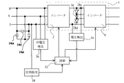
- the voltage detection circuit 34 detects the voltage between the positive direct current intermediate link 4p and the negative intermediate link 4n. A signal representing the detected voltage is supplied to the control circuit 32, and the potential difference Vc between both ends of the snubber capacitor 30 is calculated.
- phase voltages Vr, Vs, and Vt which are the voltages of the three power supplies included in the three-phase AC power supply, are detected by the phase voltage detector 36 and the detection results are supplied to the control circuit 32. Furthermore, the phase detector 38 detects the phase of any one of the three-phase AC power sources, for example, the T-phase power source in this embodiment, and the detection result is supplied to the control circuit 32.
- the control circuit 32 performs the processing shown in FIG. 3 every time the phase is advanced by 60 degrees from the reference phase, for example, the phase of the R-phase power supply as shown in FIG. Execute.
- the control circuit 32 first determines whether the potential difference between both ends of the snubber capacitor 30 is equal to or smaller than a predetermined value, that is, whether the snubber capacitor 30 needs to be charged (step 2). When the answer to this determination is no, that is, when charging is not necessary, the control circuit 32 stops the charging process of the snubber capacitor 30 and starts the next process, for example, control of the converter 2 and the inverter 4 not shown.
- the control circuit 32 determines whether or not the potential difference between the two-phase power sources determined in advance is substantially the same as the potential difference of the snubber capacitor 30. (Step S4).
- the potential difference between the predetermined two-phase power sources is the phase voltage Vs and the phase voltage in the section 1 from the reference phase of phase 0 degrees (the phase of the R-phase power supply is 90 degrees) to 60 degrees.
- the potential difference Vst from the voltage Vt is a potential difference Vsr between the phase voltage Vs and the phase voltage Vr in the interval 2 from 60 degrees to 120 degrees, and the phase voltage Vt and the phase voltage r in the section 3 from 120 degrees to 180 degrees.
- Is a potential difference Vts between the phase voltage Vt and the phase voltage Vs in the section 4 from 180 degrees to 240 degrees, and is between the phase voltage Vr and the phase voltage Vs in the section 5 from 240 degrees to 300 degrees.
- the potential difference Vrs is a potential difference Vrt between the phase voltage Vr and the phase voltage Vt in the section 6 from 300 degrees to 0 degrees.
- step S4 is repeated until the answer is yes. If the answer to the determination in step S4 is yes, the upper bidirectional switch circuit connected to the rising phase power source of the two phase voltages is turned on, and the lower side connected to the falling phase power source The direction switch circuit is turned on (step S6).
- step S6 When the determination in step S6 is yes, charging of the snubber capacitor 30 is started. That is, step S6 functions as a charging start step. Since the potential difference of the snubber capacitor 30 and the two-phase potential difference for charging the snubber capacitor 30 are substantially equal at the start of charging, a large inrush current does not flow through the snubber capacitor 30.
- step S8 determines whether the remaining one phase is 0V (step S8). If the answer to this determination is no, step S8 is repeated until the answer is yes. During this time, the charging of the snubber capacitor 30 is continued. Then, when the answer to the determination in step S8 is yes, the potential difference between the two phases, that is, Vst is the maximum in the section 1, and even if charged more than this, it is not charged depending on the potential difference between the two phases. End the processing in the section. That is, step S8 functions as a charging completion determination step.
- the next section for example, section 2 is started.
- the upper bidirectional switch 8us that is turned on is common.
- the lower bidirectional switch 8dr that is turned on is common to the sections 2 and 3
- the upper bidirectional switch 8ut that is turned on is common to the sections 3 and 4, and is turned on to the sections 4 and 5.
- the lower bidirectional switch 8ds is common, the upper switches 8ur that are turned on are common in the sections 5 and 6, and the lower bidirectional switch 8dt that is turned on is common in the sections 6 and 1. Therefore, problems such as short circuit do not occur.
- the snubber capacitor 30 By charging the snubber capacitor 30 when the power is turned on, it is possible to prevent a large inrush current from flowing through the snubber capacitor 30. Moreover, since it is not necessary to limit the inrush current using a resistor, the time required for charging can be shortened, and the time until the switching operation of the converter 2 can be drastically shortened. Specifically, for example, in section 1, if the charging time is the longest, charging starts at the beginning of section 1 (phase 0 degree) and charging ends when the R phase reaches 0V. However, at the end of this section, it is 90 degrees in terms of phase, and the charging time does not become longer than this.
- the maximum charging time is a time when the phase changes by 90 degrees, and the time until the switching operation of the converter 2 is started can be drastically shortened. Further, since it is not necessary to use a resistor or a switch for intermittently connecting the resistor to the snubber capacitor, it is not necessary to add a new part.
- charging of the snubber capacitor is started when the potential difference between both ends of the snubber capacitor 30 becomes substantially equal to the predetermined two-phase potential difference in each section, but the predetermined two-phase voltage is The snubber capacitor can be charged as soon as they are almost equal. In this case, there may be a difference between the potential difference between both ends of the snubber capacitor 30 and a predetermined two-phase voltage, but the snubber capacitor 30 is charged from the state where the two-phase potential difference is almost zero. A too large inrush current does not flow through the snubber capacitor 30.
- the snubber capacitor 30 can be charged by these two phases.
- both ends of the snubber capacitor measured before the charging is started. Charge to a predetermined voltage based on the potential difference between the two phases, the phase of the two phases at the start of charging (the phase difference with respect to the reference phase (which is determined from the phase detection result of the phase detector 38), and the frequency of the three-phase AC power supply. It is also possible to calculate the time required for the charging, and when the time has elapsed, it can be determined that the charging time has elapsed and charging can be stopped.
- the snubber capacitor 30 is connected to the positive side DC intermediate link 4p and the negative side DC intermediate link 4n via the clamp diodes 28u and 28d.
- the clamp diodes 28u and 28d are removed and the positive side DC intermediate link is connected. It can also be connected to the link 4p and the negative side DC intermediate link 4n.
- the present invention is implemented in a matrix converter.
- the present invention is not limited to this.
- the present invention can be implemented when a normal converter and an inverter are used in combination, or only a converter is used. It can also be implemented.
Landscapes
- Engineering & Computer Science (AREA)
- Power Engineering (AREA)
- Ac-Ac Conversion (AREA)
- Inverter Devices (AREA)
Abstract
【解決手段】 インダイレクトマトリクスコンバータ1の中間直流母線4p、4n間に接続されたスナバコンデンサ30の両端間電位差が、三相交流電源の投入時に検出される。この検出結果に基づいて三相交流電源の各相のうち、スナバコンデンサ30の電位差とほぼ同じ電位差になる二相を判定する。この二相のうち電圧が上昇する相を、スナバコンデンサ30の正極に、前記二相のうち電圧が降下する相を、前記スナバコンデンサの負極にインダイレクトマトリクスコンバータ1を介して接続する。
Description
本発明は、半導体スイッチング回路において過電圧保護のために設けるスナバコンデンサの充電方法に関する。
スナバコンデンサは、過電圧保護のために使用されるが、その過電圧の発生原因の1つとして、例えば電源投入時に流れる突入電流がある。この突入電流を制限するために、例えば特許文献1に開示されている技術では、抵抗器によって突入電流を制限している
特許文献1の技術によれば、突入電流を制限することができるが、抵抗器によって電流を制限している関係上、突入電流を完全にスナバコンデンサに充電するための充電時間が長くなる。この充電が完了するまで、スイッチング回路がスイッチングを開始できない。
本発明は、突入電流の充電時間を短くすることができるスナバコンデンサの充電方法を提供することを目的とする。
本発明の一態様のスナバコンデンサの充電方法では、三相交流電源をスイッチングするスイッチング回路の母線間に接続されたスナバコンデンサの両端間電位差を、前記三相交流電源の投入時に検出する。この検出結果に基づいて前記三相交流電源の各相電圧のうち、前記スナバコンデンサの電位差と同じ電位差になる二相を判定する。この二相のうち電圧が上昇する相を、前記スナバコンデンサの正極に前記スイッチング回路を介して接続すると共に、前記二相のうち電圧が降下する相を、前記スナバコンデンサの負極に前記スイッチング回路を介して接続する。スイッチング回路としては、例えば三相交流電源を整流するコンバータと、この整流された直流を所望の周波数及び電圧の三相交流電源に変換するインバータとの組合せを使用することもできる。この場合、スナバコンデンサは、コンバータの出力側に設けられる。或いは、三相交流電源の電圧及び周波数を変換するインダイレクトマトリクスコンバータを使用することもできる。この場合、スナバコンデンサは、インダイレクトマトリクスコンバータのコンバータ部とインバータ部との間に接続される。これらスイッチング回路は、自己消弧能力を備えた半導体スイッチング素子、例えばバイポーラトランジスタ、MOSFETまたはIGFETからなるブリッジ回路を使用することができる。
この充電方法によれば、スナバコンデンサの両端間電位差と、ほぼ同じ電位差の二相電圧間にスナバコンデンサが接続されるので、過電流が殆ど流れることがない。しかも、三相交流電源を抵抗器を介さずにスナバコンデンサに接続しているので、短時間でスナバコンデンサを充電することができる。
本発明の他の態様のスナバコンデンサの充電方法は、三相交流電源をスイッチングするスイッチング回路において、前記三相交流電源の投入時に、前記三相交流電源の各相電圧のうち、電圧が同じになる二相を判定する。この二相のうち電圧が上昇する相を、前記スイッチング回路中にあるスナバコンデンサの正極に前記スイッチング回路を介して接続すると共に、前記二相のうち電圧が降下する相を、前記スナバコンデンサの負極に前記スイッチング回路を介して接続する。スイッチング回路としては、上記の態様と同様にコンバータやマトリクスコンバータのコンバータ部を使用することができ、スイッチング回路のスイッチング素子としては、上記の態様と同様にバイポーラトランジスタ、MOSFETまたはIGFETを使用することができる。
この充電方法では、三相交流電源の二相の電圧が同じ、即ち電位差が零ボルトのときに、その二相にスナバコンデンサを接続しているので、過電流が殆ど流れず、スナバコンデンサの充電時間を短縮することができる。
前記スナバコンデンサが充電されたことを判断する充電完了判定ステップを備えることもできる。この充電完了判定ステップは、前記三相交流電源の周波数と前記スナバコンデンサの充電前の電位差から充電時間を算出し、充電時間が経過したことを判定するものとすることができる。
このように構成すると、スナバコンデンサが充分に充電された後に、次のステップ、例えばスイッチング回路によるスイッチングを開始することができる。
充電完了判定ステップとしては、前記スナバコンデンサの電位差が所定値以上になったことを判定するものとすることもできる。このように構成すると、過剰な突入電流が流れない程度に、スナバコンデンサの電位差が所定値以上になった後に、次のステップに移行することができるので、この移行を早期に行うことができる。
或いは、充電完了判定ステップとしては、前記三相交流電源の残りの相が零ボルトになったことを判定するものを使用することもできる。このように構成すると、残りの相の電圧が零ボルトのとき、スナバコンデンサの両端に接続された二相は最大の電位差になっているので、スナバコンデンサに充分に充電することができる。
上記の各態様のいずれかにおいて、スナバコンデンサへの充電開始前に、前記スナバコンデンサの電位差が所定値以上あるとき、前記スナバコンデンサの充填ステップを省くスことができる。即ち、このスナバコンデンサの充填は、スナバコンデンサの両端間電位差が所定値未満の時に行われる。これによって、危険な突入電流が発生しない程に、スナバコンデンサが充電されているときには、充電ステップを省くことができ、次のステップへの移行を速やかに行える。
本発明の1実施形態のスナバコンデンサの充電方法は、図1に示すようなインダイレクトマトリクスコンバータ1において、行われる。このインダイレクトマトリクスコンバータは、コンバータ2と、正極側直流中間リンク4p、負極側直流中間リンク4nと、インバータ6とを有している。
コンバータ2は、上側アームとして上側双方向スイッチ回路8ur、8us、8utを有し、下側アームとして下側双方向スイッチ回路8dr、8ds、8dtを有している。上側双方向スイッチ回路8urと下側双方向スイッチ回路8drとが直列に接続され、上側双方向スイッチ回路8usと下側双方向スイッチ回路8dsとが直列に接続され、上側双方向スイッチ回路8utと下側双方向スイッチ回路8dtとが直列に接続されている。これら3つの直列回路が互いに並列に接続されている。上側及び下側双方向スイッチ回路8ur、8drは、共に単方向スイッチ素子、例えばIGBT10a、10bを有している。これらのエミッタ同士が接続され、それぞれのコレクタ-エミッタ間に逆並列にダイオード12a、12bが接続されている。上側双方向スイッチ回路8urのIGBT10aが、正極性直流中間リンク4pに接続されている。上側双方向スイッチ回路8urのIGBT10bが、下側双方向スイッチ回路8drのIGBT10aのコレクタに接続されている。下側双方向スイッチ回路8dのIGBT10bが、負極性直流中間リンク4nに接続されている。他の上側双方向スイッチ回路8us、8ut、下側双方向スイッチ回路8ds、8dtも同様に構成されている。
上側双方向スイッチ回路8urと下側双方向スイッチ回路8drとの接続点Rinには、三相交流電源13のR相電源が直流リアクトル15Rを介して接続され、上側双方向スイッチ回路8usと下側双方向スイッチ回路8dsとの接続点Sinには、三相交流電源13のS相電源が直流リアクトル15Sを介して接続され、上側双方向スイッチ回路8utと下側双方向スイッチ回路8dtとの接続点Tinには、三相交流電源13のT相電源が直流リアクトル15Tを介して接続されている。接続点Rin、Sin間にはコンデンサ14rsが、接続点Sin、Tin間にはコンデンサ14stが、接続点Tin、Rin間にはコンデンサ14trが接続されている。これらコンデンサ14rs、14st、14trと各直流リアクトル15R、15S、15Tとによって入力フィルタが構成されている。
インバータ6は、上側アームとして単方向スイッチ素子、例えばIGBT16uu、16uv,16uwを有し、下側アームとして単方向スイッチ素子、例えばIGBT16du、16dv、16dwを有している。IGBT16uuのコレクタが正極性直流中間リンク4pに接続されている。IGBT16uuのエミッタがIGBT16duのコレクタに接続されている。IGBT16duのエミッタが負極性直流中間リンク4nに接続されている。即ち、IGBT16uu、16duの直列回路が中間直流リンク4p、4n間に接続されている。他のIGBT16uv、16uw、16dv、16dwも同様に接続されている。IGBT16uu、16uv、16uwのコレクタ-エミッタ間には逆並列にダイオード18uが接続されている。IGBT16du、16dv、16dwのコレクタ-エミッタ間にも逆並列にダイオード18dが接続されている。IGBT16uu、16duとの接続点u、IGBT16uv、16dvの接続点v、IGBT16uw、16dwの接続点wには、負荷、例えば電動アクチュエータ19が接続されている。
各IGBT16uu、16uv、16uwには、放電阻止形スナバ回路20uが接続されている。各IGBT16du、16dv、16dwには、放電阻止スナバ回路20dが接続されている。各放電阻止形スナバ回路20uでは、IGBT16uu、16uv、16uwのコレクタ-エミッタ間に、スナバコンデンサ22uとスナバダイオード24uとの直列回路が並列に接続されている。具体的には、各スナバコンデンサ22uの一端がIGBT16uu、16uv、16uwのコレクタに接続され、各スナバコンデンサ22uの他端が各スナバダイオード24uのアノードにそれぞれ接続されている。各スナバダイオード24uのカソードがIGBT16uu、16uv、16uwのエミッタに接続されている。各スナバコンデンサ22uと各スナバダイオード24uとの接続点に各スナバ放電抵抗器26uの一端が接続され、他端が後述するスナバコンデンサ30とダイオード28dのアノードとの接続点に接続されている。
放電阻止形スナバ回路20dでは、IGBT16du、16dv、16dwのコレクタ-エミッタ間に、スナバコンデンサ22dとスナバダイオード24dとの直列回路が並列に接続されている。具体的には、各スナバダイオード24dのアノードがIGBT16du、16dv、16dwのコレクタに接続され、各スナバダイオード24dのカソードが各スナバコンデンサ22dの一端に接続され、各スナバコンデンサ22dの他端がIGBT16du、16dv、16dwのエミッタに接続されている。各スナバコンデンサ22dと各スナバダイオード24dとの接続点に各スナバ放電抵抗器26dの一端が接続され、各スナバ放電抵抗器26dの他端がスナバコンデンサ30と後述するダイオード28uのカソードとの接続点に接続されている。
コンバータ2の上側及び下側双方向スイッチ回路8ur、8us、8ut、8dr、8ds、8dt及びインバータ6のIGBT16uu、16uv、16uw、16du、16dv、16dwは、図2に示す制御回路32によってオンオフ制御される。特に、各上側及び下側双方向スイッチ回路8ur、8us、8ut、8dr、8ds、8dtの切換は、インバータ6の環流期間、即ち、インバータ6のIGBT16uu、16uv、16uwがオンで、IGBT16du、16dv、16dwがオフの状態で、またはインバータ6のIGBT16uu、16uv、16uwがオフで、IGBT16du、16dv、16dwがオンの状態で、これから切り換えられる線間電圧が零の時点で行われる。
また、図1に示すように、正極性直流中間リンク4pに上側電圧降下手段、例えばクランプダイオード28uのアノードが接続され、それのカソードにスナバコンデンサ30の一端が接続されている。スナバコンデンサ30の他端に、下側電圧降下手段、例えばクランプダイオード28dのアノードが接続され、そのカソードが負極側直流中間リンク4nに接続されている。上述したように各スナバ放電抵抗器26uの他端が、スナバコンデンサ30とダイオード28dのアノードとの接続点に接続され、各スナバ放電抵抗器26dの他端が、スナバコンデンサ30とダイオード28uのカソードとの接続点に接続されている。
各放電形スナバ回路20uが設けられているIGBT、例えばIGBT16uvがターンオンしていたのがターンオフする際、今までIGBT16uvに流れていた電流が、スナバコンデンサ22u、ダイオード24uを介して流れる。このとき、配線インダクタンスとターンオフ時の電流とによって決まるエネルギーがスナバコンデンサ22uに吸収され、スナバコンデンサ22uの電圧を上昇させる。その結果、IGBT16uvの寄生容量によるサージ電圧の発生を防止する。スナバコンデンサ22uの電圧は、正極性直流リンク4pの電圧よりも高いとき、正極性直流リンク4p、コンバータ2、負極性直流リンク4n及びいずれかオンしているIGBT16du、16dv、16dwの経路を経て、次にIGBT16uvがターンオンするまでに放電される。放電形スナバ回路20dにおいても、電流の流れる方向は、放電形スナバ回路20uと逆であるが、同様にしてサージの発生が防止される。このように放電形スナバ回路20u、20dは、インバータ6でのスイッチング動作時に発生するサージを防止している。
また、コンバータ2でのスイッチング動作によって、インバータ6のIGBT16uu、16uv、16uwにおいてサージが発生することを防止するために、上述したように、各スナバコンデンサ22uと各スナバダイオード24uとの接続点に一端が接続された各スナバ放電抵抗器26uの他端がスナバコンデンサ30とダイオード28dのアノードとの接続点に接続され、各スナバコンデンサ22dと各スナバダイオード24dとの接続点に一端が接続された各スナバ放電抵抗器26dの他端が、スナバコンデンサ30とダイオード28uのカソードとの接続点に接続されている。
即ち、コンデンサ14rs、14st、14trが、三相交流電源の各線間電圧にほぼ等しく充電され、スナバコンデンサ30もこれら線間電圧にほぼ充電されている状態では、スナバコンデンサ30と上側のクランプダイオード28uのカソードとの接続点の電位は、三相交流電源の相間電圧Vrs、Vst、Vtsの絶対値のピーク電位からクランプダイオード28uでの電圧降下分を差し引いた電位にクランプされ、コンデンサ30と下側のクランプダイオード28dのアノードとの接続点の電位は、三相交流電源の相間電圧Vrs、Vst、Vtsの絶対値のクロス電位にクランプダイオード28dの電圧降下分を加算した電位にクランプされ、変動しない。
このように電位が変動しないコンデンサ30と上側のクランプダイオード28uのカソードとの接続点に、下側の放電阻止形スナバ回路20dのスナバ放電抵抗器26dの他端が接続され、電位が変動しないコンデンサ30と下側のクランプダイオード28dのアノードとの接続点に、上側の放電阻止形スナバ回路20uのスナバ放電抵抗器26uの他端が接続されている。従って、直流中間電位がコンバータ2でのスイッチングによって変動しても、スナバコンデンサ22uは、コンデンサ30とクランプダイオード28dのアノードとの接続点の電位までしか放電せず、スナバコンデンサ22dは、コンデンサ30とクランプダイオード28uのカソードとの接続点の電位までしか放電しない。そのため、コンバータ2でスイッチングしても、スナバコンデンサ22uの電位が、コンデンサ14rs、14st、14trの電位よりも低くなることはなく、これらコンデンサ14rs、14st、14trからスナバコンデンサ22uに電流が流れず、サージが発生することはない。
このようにサージの発生を防止するためには、スナバコンデンサ30が充電されている必要がある。そのため、このインダイレクトマトリクスコンバータ1へ三相交流電源の電圧供給を開始した時点でコンバータ2によってスナバコンデンサ30を充電する必要がある。このとき、大きな突入電流が流れる虞がある。大きな突入電流が流れることなく、スナバコンデンサ30を充電するために、以下のような構成が採用されている。
図2に示すように、電圧検出回路34によって、正極性直流中間リンク4p及び負極性中間リンク4n間の電圧が検出されている。検出された電圧を表す信号が制御回路32に供給され、スナバコンデンサ30の両端間の電位差Vcが算出される。
また、三相交流電源が備える3つの電源の電圧である各相電圧Vr、Vs、Vtが相電圧検出器36によってそれぞれ検出され、その検出結果が制御回路32に供給されている。さらに、三相交流電源の各電源のうちいずれか、例えばこの実施形態ではT相電源の位相が位相検出器38によって検出され、その検出結果が制御回路32に供給されている。
制御回路32は、位相検出器38による位相検出結果に従って、図4に示すように基準となる位相、例えばR相電源の位相が90度から、位相が60度進むごとに、図3に示す処理を実行する。
図3に示す処理では、制御回路32は、まずスナバコンデンサ30の両端間の電位差が予め定めた所定値以下であるか、即ちスナバコンデンサ30の充電が必要であるか判断する(ステップ2)。この判断の答えがノーの場合、即ち充電不要の場合、制御回路32はスナバコンデンサ30の充電処理を中止し、次の処理、例えば図示していないコンバータ2及びインバータ4の制御を開始する。
ステップS2の判断の答えがイエスの場合、即ち、スナバコンデンサ30の充電が必要な場合、制御回路32は、予め定めた2相の電源の電位差がスナバコンデンサ30の電位差とほぼ同じであるか判断する(ステップS4)。予め定めた2相の電源の電位差は、例えば、図4に示すように基準位相である位相0度(R相電源の位相が90度)から60度までの区間1では、相電圧Vsと相電圧Vtとの電位差Vstであり、60度から120度の区間2では、相電圧Vsと相電圧Vrとの電位差Vsrであり、120度から180度の区間3では、相電圧Vtと相電圧rとの電位差Vtrであり、180度から240度の区間4では、相電圧Vtと相電圧Vsとの電位差Vtsであり、240度から300度の区間5では、相電圧Vrと相電圧Vsとの電位差Vrsであり、300度から0度の区間6では、相電圧Vrと相電圧Vtとの電位差Vrtである。
このステップS4の判断の答えがノーであると、答えがイエスになるまでステップS4が繰り返される。ステップS4の判断の答えがイエスであると、2つの相電圧のうち上昇する相の電源に接続されている上側双方向スイッチ回路をオンし、下降する相の電源に接続されている下側双方向スイッチ回路をオンする(ステップS6)。
例えば、区間1では、相電圧Vsが上昇し、相電圧Vtが降下しているので、上側双方向スイッチ回路8usと下側双方向スイッチ回路8dtとがオンされる。
区間2では相電圧Vsが上昇し、相電圧Vrが降下するので、上側双方スイッチ8usがオンされ、下側双方向スイッチ8drがオンされる。
区間3では、相電圧Vtが上昇し、相電圧Vrが低下するので、上側双方向スイッチ8utがオンされ、下側双方向スイッチ8drがオンされる。
区間4では相電圧Vtが上昇し、相電圧Vsが降下するので、上側双方向スイッチ8utがオンされ、下側双方向スイッチ8dsがオンされる。
区間5では、相電圧Vrが上昇し、相電圧Vsが降下するので、上側双方向スイッチ8urがオンされ、下側双方向スイッチ8dsがオンされる。
区間6では、相電圧Vrが上昇し、相電圧Vtが降下するので、上側双方向スイッチ8urがオンされ、下側双方向スイッチ8dtがオンされる。
ステップS6の判断がイエスになったことにより、スナバコンデンサ30の充電が開始される。即ち、ステップS6は充電開始ステップとして機能する。充電の開始時点で、スナバコンデンサ30の電位差と、スナバコンデンサ30を充電する2相の電位差とはほぼ等しいので、大きな突入電流がスナバコンデンサ30に流れることはない。
ステップS6に続いて、残りの一相が0Vであるか判断される(ステップS8)。この判断の答えがノーであると、イエスになるまでステップS8が繰り返される。この間、スナバコンデンサ30への充電が継続される。そして、ステップS8の判断の答えがイエスになったとき、2相の電位差、区間1で言えばVstが最大であり、これ以上充電しても、この2相の電位差によっては充電されないので、その区間での処理を終了する。即ち、ステップS8は充電完了判定ステップとして機能する。
なお、1つの区間、例えば区間1が終了する前に、次の区間、例えば区間2が開始されるが、例えば区間1と区間2とではオンされる上側双方向スイッチ8usが共通であり、区間2と区間3とでオンされる下側双方向スイッチ8drが共通であり、区間3と区間4とではオンされる上側双方向スイッチ8utが共通であり、区間4と区間5とではオンされる下側双方向スイッチ8dsが共通であり、区間5と区間6とではオンされる上側双方スイッチ8urが共通であり、区間6と区間1とではオンされる下側双方向スイッチ8dtが共通であるので、短絡などの問題は生じない。
このようにスナバコンデンサ30を電源投入時に充電することにより、スナバコンデンサ30に大きな突入電流が流れることを防止できる。しかも、抵抗器を使用して突入電流を制限する必要がないので、充電に要する時間を短縮することができ、コンバータ2のスイッチチング動作開始までの時間を飛躍的に短縮することができる。具体的には、例えば区間1で言えば、充電時間が最も長い場合は、区間1の当初(位相0度)に充電が開始されて、R相が0Vとなる時点で充電が終了した場合であるが、この区間の終了時は位相で言えば90度であり、これ以上に充電時間が長くなることはない。即ち、最大充電時間は、位相が90度変化する時間であり、コンバータ2のスイッチング動作開始までの時間を飛躍的に短縮することができる。また、抵抗器やこれをスナバコンデンサに対して断続するためのスイッチを使用する必要がないので、新たな部品を追加する必要が無い。
上記の実施形態では、各区間において、スナバコンデンサ30の両端間電位差が、予め定めた2相の電位差とほぼ等しくなったときからスナバコンデンサの充電を開始したが、予め定めた2相の電圧がほぼ等しくなると直ちにスナバコンデンサの充電を開始することもできる。この場合、スナバコンデンサ30の両端間電位差と、予め定めた2相の電圧との間には差があることもあるが、2相の電位差がほぼ零の状態からスナバコンデンサ30が充電されるので、余り大きな突入電流がスナバコンデンサ30に流れることはない。また、予め定めた2相の電圧がほぼ等しく無い状態であっても、これら2相の電位差とスナバコンデンサ30の両端間電位差との差が過剰な突入電流が発生しない程度の差であれば、これら2相によってスナバコンデンサ30を充電することもできる。
上記の実施形態では、スナバコンデンサ30の充電に関与していない相の電圧が0Vになったとき、充電完了と判定して、充電を停止させたが、充電開始前に測定したスナバコンデンサの両端間電位差と、充電開始時の2相の位相(基準位相に対する位相差(これは位相検出器38の位相検出結果から判明する)と三相交流電源の周波数とから予め定めた電圧まで充電するのに要する時間を算出し、その時間が経過したとき、充電時間が経過したと判断して、充電を停止させることもできる。
上記の実施形態では、ナバコンデンサ30の充電に関与していない相の電圧が0Vになったとき、充電完了と判定して、充電を停止させたが、電圧検出器34によって測定したスナバコンデンサ30の電位差が所定値以上になったと制御回路32が判定したとき、充電を停止するように構成することもできる。
上記の実施形態では、スナバコンデンサ30をクランプダイオード28u、28dを介して正極側直流中間リンク4p、負極側直流中間リンク4nに接続したが、これらクランプダイオード28u、28dを除去して正極側直流中間リンク4p、負極側直流中間リンク4nに接続することもできる。上記の実施形態では、本発明をマトリクスコンバータに実施したが、これに限ったものではなく、例えば通常のコンバータとインバータとを組み合わせて使用する場合にも実施することができるし、コンバータのみを使用する場合にも実施できる。
Claims (6)
- 三相交流電源をスイッチングするスイッチング回路の母線間に接続されたスナバコンデンサの両端間電位差を、前記三相交流電源の投入時に検出する過程と、
この検出結果に基づいて前記三相交流電源の各相電圧のうち、前記スナバコンデンサの電位差と同じ位相差になる二相の電圧を判定し、
この二相のうち電圧が上昇する相の電源を、前記スナバコンデンサの正極に前記スイッチング回路を介して接続すると共に、前記二相のうち電圧が降下する相の電源を、前記スナバコンデンサの負極に前記スイッチング回路を介して接続する
スナバコンデンサの充電方法。 - 三相交流電源をスイッチングするスイッチング回路において、前記三相交流電源の投入時に、前記三相交流電源の各相電圧のうち、値が同じになる二相の電圧を判定し、
この二相のうち電圧が上昇する相の電源を、前記スイッチング回路中にあるスナバコンデンサの正極に前記スイッチング回路を介して接続すると共に、前記二相のうち電圧が降下する相の電源を、前記スナバコンデンサの負極に前記スイッチング回路を介して接続する
スナバコンデンサの充電方法。 - 請求項1または2記載のスナバコンデンサの充電方法において、
前記スナバコンデンサが充電されたことを判断する充電完了判定ステップを備え、この充電完了判定ステップは、前記三相交流電源の周波数と前記スナバコンデンサの充電前の電位差から充電時間を算出し、充電時間が経過したことを判定する
スナバコンデンサの充電方法。 - 請求項1または2記載のスナバコンデンサの充電方法において、
前記スナバコンデンサが充電されたことを判断する充電完了判定ステップを備え、この充電完了判定ステップは、前記スナバコンデンサの電位差が所定値以上になったことを判定するスナバコンデンサの充電方法。 - 請求項1または2記載のスナバコンデンサの充電方法において、
前記スナバコンデンサが充電されたことを判断する充電完了判定ステップを備え、この充電完了判定ステップは、前記三相交流電源の残りの相が零ボルトになったことを判定するスナバコンデンサの充電方法。 - 請求項1乃至5いずれか記載のスナバコンデンサの充電方法において、
前記スナバコンデンサへの充電開始前に、前記スナバコンデンサの電位差が所定値以上あるとき、前記スナバコンデンサの充填ステップを省くスナバコンデンサの充電方法。
Applications Claiming Priority (2)
| Application Number | Priority Date | Filing Date | Title |
|---|---|---|---|
| JP2011058968A JP2012196072A (ja) | 2011-03-17 | 2011-03-17 | スナバコンデンサの充電方法 |
| JP2011-058968 | 2011-03-17 |
Publications (1)
| Publication Number | Publication Date |
|---|---|
| WO2012124510A1 true WO2012124510A1 (ja) | 2012-09-20 |
Family
ID=46830585
Family Applications (1)
| Application Number | Title | Priority Date | Filing Date |
|---|---|---|---|
| PCT/JP2012/055363 Ceased WO2012124510A1 (ja) | 2011-03-17 | 2012-03-02 | スナバコンデンサの充電方法 |
Country Status (2)
| Country | Link |
|---|---|
| JP (1) | JP2012196072A (ja) |
| WO (1) | WO2012124510A1 (ja) |
Cited By (1)
| Publication number | Priority date | Publication date | Assignee | Title |
|---|---|---|---|---|
| CN112271800A (zh) * | 2020-10-16 | 2021-01-26 | 珠海格力电器股份有限公司 | 一种无充电回路的供电电路及电源管理系统 |
Citations (4)
| Publication number | Priority date | Publication date | Assignee | Title |
|---|---|---|---|---|
| JPH1175370A (ja) * | 1997-08-29 | 1999-03-16 | Denso Corp | 交直変換装置 |
| JP2002142458A (ja) * | 2000-10-31 | 2002-05-17 | Fuji Electric Co Ltd | 整流回路及びその制御方法 |
| JP2006109582A (ja) * | 2004-10-04 | 2006-04-20 | Yaskawa Electric Corp | マトリクスコンバータ |
| JP2007129875A (ja) * | 2005-11-07 | 2007-05-24 | Denso Wave Inc | 突入電流防止回路 |
-
2011
- 2011-03-17 JP JP2011058968A patent/JP2012196072A/ja not_active Withdrawn
-
2012
- 2012-03-02 WO PCT/JP2012/055363 patent/WO2012124510A1/ja not_active Ceased
Patent Citations (4)
| Publication number | Priority date | Publication date | Assignee | Title |
|---|---|---|---|---|
| JPH1175370A (ja) * | 1997-08-29 | 1999-03-16 | Denso Corp | 交直変換装置 |
| JP2002142458A (ja) * | 2000-10-31 | 2002-05-17 | Fuji Electric Co Ltd | 整流回路及びその制御方法 |
| JP2006109582A (ja) * | 2004-10-04 | 2006-04-20 | Yaskawa Electric Corp | マトリクスコンバータ |
| JP2007129875A (ja) * | 2005-11-07 | 2007-05-24 | Denso Wave Inc | 突入電流防止回路 |
Cited By (2)
| Publication number | Priority date | Publication date | Assignee | Title |
|---|---|---|---|---|
| CN112271800A (zh) * | 2020-10-16 | 2021-01-26 | 珠海格力电器股份有限公司 | 一种无充电回路的供电电路及电源管理系统 |
| US12609538B2 (en) | 2020-10-16 | 2026-04-21 | Gree Electric Appliances, Inc. Of Zhuhai | Energy management system including a power supply circuit without a charging loop |
Also Published As
| Publication number | Publication date |
|---|---|
| JP2012196072A (ja) | 2012-10-11 |
Similar Documents
| Publication | Publication Date | Title |
|---|---|---|
| JP5528946B2 (ja) | インダイレクトマトリクスコンバータ | |
| US10128741B2 (en) | Power conversion device | |
| CN101953062B (zh) | 电力转换装置 | |
| JP6261491B2 (ja) | 電力変換装置 | |
| CN102545639B (zh) | 用于调节直流电压的电路和方法以及电力转换器 | |
| US9787084B2 (en) | Motor driving device | |
| JP6526344B2 (ja) | 電力変換装置および電力システム | |
| JP5049964B2 (ja) | 電力変換装置 | |
| US20160036342A1 (en) | Power conversion device | |
| US10587203B2 (en) | Power conversion apparatus | |
| JP2013215043A (ja) | マルチレベル電力変換装置 | |
| US10069438B2 (en) | Power converter with capacitor voltage balancing | |
| US8995152B2 (en) | Inverter circuit | |
| EP1643626A2 (en) | Direct current power supply apparatus and control method for the same, and a compressor drive apparatus | |
| JP5302905B2 (ja) | 電力変換装置 | |
| WO2012124510A1 (ja) | スナバコンデンサの充電方法 | |
| JP6700578B2 (ja) | 無停電電源装置 | |
| KR102419754B1 (ko) | 전력 변환 장치 | |
| CN108462380B (zh) | 减轻无变压器整流器ups系统中ac输入电压浪涌影响的方法 | |
| JP2015202033A (ja) | マルチレベル電力変換回路 | |
| WO2020213317A1 (ja) | 電力変換装置 | |
| JP2016127677A (ja) | 電力変換装置 | |
| JP2019176652A (ja) | 電力変換装置、蓄電装置、及び、電力変換装置の制御方法 | |
| Yuan et al. | Safe stop-pulsing strategy for IGCT-based three-level neutral point clamped inverters | |
| JP2015023601A (ja) | 電力変換装置 |
Legal Events
| Date | Code | Title | Description |
|---|---|---|---|
| 121 | Ep: the epo has been informed by wipo that ep was designated in this application |
Ref document number: 12758194 Country of ref document: EP Kind code of ref document: A1 |
|
| NENP | Non-entry into the national phase |
Ref country code: DE |
|
| 122 | Ep: pct application non-entry in european phase |
Ref document number: 12758194 Country of ref document: EP Kind code of ref document: A1 |