WO2012121349A1 - 太陽電池セル、太陽電池モジュール、太陽電池セルの製造方法及び太陽電池モジュールの製造方法 - Google Patents
太陽電池セル、太陽電池モジュール、太陽電池セルの製造方法及び太陽電池モジュールの製造方法 Download PDFInfo
- Publication number
- WO2012121349A1 WO2012121349A1 PCT/JP2012/056013 JP2012056013W WO2012121349A1 WO 2012121349 A1 WO2012121349 A1 WO 2012121349A1 JP 2012056013 W JP2012056013 W JP 2012056013W WO 2012121349 A1 WO2012121349 A1 WO 2012121349A1
- Authority
- WO
- WIPO (PCT)
- Prior art keywords
- alignment mark
- receiving surface
- line
- solar battery
- light receiving
- Prior art date
- Legal status (The legal status is an assumption and is not a legal conclusion. Google has not performed a legal analysis and makes no representation as to the accuracy of the status listed.)
- Ceased
Links
Images









Classifications
-
- H—ELECTRICITY
- H10—SEMICONDUCTOR DEVICES; ELECTRIC SOLID-STATE DEVICES NOT OTHERWISE PROVIDED FOR
- H10F—INORGANIC SEMICONDUCTOR DEVICES SENSITIVE TO INFRARED RADIATION, LIGHT, ELECTROMAGNETIC RADIATION OF SHORTER WAVELENGTH OR CORPUSCULAR RADIATION
- H10F77/00—Constructional details of devices covered by this subclass
-
- H—ELECTRICITY
- H10—SEMICONDUCTOR DEVICES; ELECTRIC SOLID-STATE DEVICES NOT OTHERWISE PROVIDED FOR
- H10F—INORGANIC SEMICONDUCTOR DEVICES SENSITIVE TO INFRARED RADIATION, LIGHT, ELECTROMAGNETIC RADIATION OF SHORTER WAVELENGTH OR CORPUSCULAR RADIATION
- H10F19/00—Integrated devices, or assemblies of multiple devices, comprising at least one photovoltaic cell covered by group H10F10/00, e.g. photovoltaic modules
- H10F19/90—Structures for connecting between photovoltaic cells, e.g. interconnections or insulating spacers
- H10F19/902—Structures for connecting between photovoltaic cells, e.g. interconnections or insulating spacers for series or parallel connection of photovoltaic cells
-
- H—ELECTRICITY
- H10—SEMICONDUCTOR DEVICES; ELECTRIC SOLID-STATE DEVICES NOT OTHERWISE PROVIDED FOR
- H10F—INORGANIC SEMICONDUCTOR DEVICES SENSITIVE TO INFRARED RADIATION, LIGHT, ELECTROMAGNETIC RADIATION OF SHORTER WAVELENGTH OR CORPUSCULAR RADIATION
- H10F77/00—Constructional details of devices covered by this subclass
- H10F77/20—Electrodes
- H10F77/206—Electrodes for devices having potential barriers
- H10F77/211—Electrodes for devices having potential barriers for photovoltaic cells
-
- Y—GENERAL TAGGING OF NEW TECHNOLOGICAL DEVELOPMENTS; GENERAL TAGGING OF CROSS-SECTIONAL TECHNOLOGIES SPANNING OVER SEVERAL SECTIONS OF THE IPC; TECHNICAL SUBJECTS COVERED BY FORMER USPC CROSS-REFERENCE ART COLLECTIONS [XRACs] AND DIGESTS
- Y02—TECHNOLOGIES OR APPLICATIONS FOR MITIGATION OR ADAPTATION AGAINST CLIMATE CHANGE
- Y02E—REDUCTION OF GREENHOUSE GAS [GHG] EMISSIONS, RELATED TO ENERGY GENERATION, TRANSMISSION OR DISTRIBUTION
- Y02E10/00—Energy generation through renewable energy sources
- Y02E10/50—Photovoltaic [PV] energy
Definitions
- the present invention relates to a solar battery cell, a solar battery module, a solar battery cell manufacturing method, and a solar battery module manufacturing method.
- This solar cell is usually formed by connecting a plurality of solar cells in series or in parallel.
- a plurality of linear electrodes (finger electrodes) made of Ag for obtaining an output are formed in parallel on the surface (light receiving surface) of the solar battery cell.
- a back electrode made of Al is formed on the back surface so as to cover the entire surface.
- a metal wiring member (TAB line) is connected to the light receiving surface of one solar cell so as to be orthogonal to all the finger electrodes, and this TAB line is connected to the other solar cell. Adjacent solar cells are connected to each other by being connected to the back electrode.
- JP 2002-263880 A JP 2004-204256 A JP-A-8-330615 JP 2003-133570 A JP 2005-243935 A JP 2007-265635 A
- solder showing good conductivity has been used for connection of TAB wires (Patent Document 1).
- Sn-Ag-Cu solder not containing Pb is sometimes used in consideration of environmental problems (Patent Documents 1 and 2).
- heat of about 220 ° C. or higher is applied to the solar cells, which may cause a decrease in the yield of the connection process and warpage of the solar cells.
- the manufacturing cost increases.
- an electrode made of Ag in advance at the position where the TAB line is arranged on the front and back surfaces of the solar battery cell. (Bus bar electrode) must be formed.
- Ag is expensive, the manufacturing cost increases.
- the electric resistance of Ag is large, if the bus bar electrode is thin, the sheet resistance of the bus bar electrode increases. If it does so, the power loss in a bus-bar electrode will increase and the power generation performance of a photovoltaic cell will fall. For this reason, in order to suppress the sheet resistance of the bus bar electrode, it is necessary to increase the width of the bus bar electrode to some extent, which further increases the manufacturing cost.
- This conductive adhesive is a composition in which metal particles such as Al particles are mixed and dispersed in a thermosetting resin, and the metal particles are sandwiched between the TAB wire and the electrode of the solar battery cell, and the electric adhesive is used. Connection is realized.
- the conductive adhesive is used for the connection of the TAB line, since the connection can be performed at 200 ° C. or lower, the yield of the connection process is reduced and the solar cell is prevented from warping. Further, when the conductive adhesive is used for the connection of the TAB wire, it is not necessary to secure the wettability, so the bus bar electrode formed for securing the wettability is not necessary, and the use of Ag is reduced. .
- the connection position of the TAB line cannot be confirmed, and there is a possibility that the TAB line cannot be attached to the planned position with high accuracy. If the TAB line cannot be pasted at a predetermined position, the array of solar cells meanders, and residual stress is generated in the solar cells, which may reduce the manufacturing yield.
- the present invention has been made in order to solve such a problem, and is capable of accurately connecting a TAB line to a predetermined position, and can suppress an increase in manufacturing cost.
- the purpose is to provide.
- a solar battery cell is a solar battery cell, and a plurality of finger electrodes arranged on a light receiving surface of a substrate and a TAB wire are bonded to the finger electrodes through a conductive adhesive.
- An alignment mark indicating a position, and the alignment mark includes a discontinuous portion on the light-receiving surface along a line intersecting with two finger electrodes located closest to opposite ends of the light-receiving surface.
- a solar cell is a solar cell in which a plurality of finger electrodes are arranged on a light receiving surface, and a TAB line is connected to the finger electrodes via a conductive adhesive,
- the alignment mark indicating the connection position of the TAB line to the finger electrode is discontinuously provided along the line intersecting the finger electrode located at both ends, and the alignment mark is connected by the same material as the finger electrode.
- the finger electrode may be integrally formed with a line width equal to or smaller than that of the TAB line.
- alignment marks indicating the connection positions of the TAB lines with respect to the finger electrodes are provided along lines intersecting the finger electrodes located at both ends. Therefore, the connection position of the TAB line can be visually confirmed by checking the alignment mark, and the TAB line can be connected to the planned position with high accuracy.
- the alignment mark is integrally formed with the finger electrode by the same material as the finger electrode. For this reason, alignment marks can be easily formed simultaneously with the finger electrodes.
- the alignment mark is formed discontinuously along the above-described line and with a line width equal to or smaller than the line width of the TAB line to be connected. Therefore, an increase in the amount of electrode material used can be suppressed as compared with a conventional solar battery cell in which continuous bus bar electrodes having the same width as the TAB line are formed. Therefore, an increase in manufacturing cost can be suppressed.
- the alignment mark may have a broken line shape. If it carries out like this, suppression of the usage-amount of an electrode material and visibility can be made compatible.
- each part of the alignment mark may extend over a plurality of finger electrodes. If it carries out like this, when test
- a plurality of alignment marks may be provided for one line. In this way, the visibility of the alignment mark is improved, and the TAB line can be accurately connected to the planned position.
- the alignment marks provided in plurality for one line may have a zigzag shape. In this way, the visibility of the alignment mark is improved, and the TAB line can be accurately connected to the planned position.
- the plurality of alignment marks provided for one line may be wider than the width of the conductive adhesive. If it carries out like this, it will become possible to visually recognize an alignment mark after adhere
- each part of the alignment mark may have a line width equal to or smaller than the line width of the finger electrode. If it carries out like this, the increase in the usage-amount of an electrode material can further be suppressed, and the increase in manufacturing cost can be suppressed.
- each part of the alignment mark may have a line width of 0.05 mm or more and 0.2 mm or less. If it carries out like this, the increase in the usage-amount of an electrode material can further be suppressed, and the increase in manufacturing cost can be suppressed.
- the solar battery module of one aspect of the present invention a plurality of the above-described solar battery cells are arranged, and the finger electrode of one adjacent solar battery cell and the back electrode formed on the back face of the other solar battery cell
- the TAB wires are connected via a conductive adhesive so as to follow the alignment mark.
- the TAB line is accurately connected to the planned position, it is possible to suppress meandering of the rows of solar cells. Thereby, when manufacturing a solar cell module, it can suppress that a residual stress generate
- a solar battery module includes a plurality of the above-described solar battery cells, and the TAB line is disposed along an alignment mark of one of the solar battery cells, and is electrically conductive. It is connected to the finger electrode of one photovoltaic cell via an adhesive, and the TAB line may be further connected to a back electrode formed on the back surface of another photovoltaic cell among the plurality of photovoltaic cells.
- a method for manufacturing a solar cell comprising preparing a substrate having a region having a predetermined width and a plurality of finger electrodes arranged on a light receiving surface that receives a conductive adhesive having the same width as the region.
- An alignment mark indicating a position to which the TAB line connected to the finger electrode is connected is provided on the light receiving surface before or after the plurality of finger electrodes are formed.
- the manufacturing method of the solar cell module of 1 side of this invention is a manufacturing method of a solar cell module, Comprising: The 1st step which prepares several above-mentioned photovoltaic cells, and a TAB line
- the present invention it is possible to provide a solar cell that can accurately connect a TAB line to a predetermined position and can suppress an increase in manufacturing cost.
- FIG. 4 is a schematic side view of FIG. 3. It is a top view which shows the light-receiving surface of the photovoltaic cell which concerns on 2nd Embodiment of this invention. It is a top view which shows the light-receiving surface of the photovoltaic cell which concerns on 3rd Embodiment of this invention.
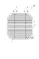
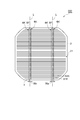
- FIG. 1 is a plan view showing a light receiving surface of a solar cell according to the first embodiment of the present invention
- FIG. 2 is a bottom view showing the back surface of the solar cell in FIG. 1
- FIG. 3 is a plurality of solar cells in FIG.
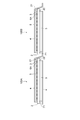
- FIG. 4 is a schematic side view of FIG. 3.
- a plurality of solar cells 100 are electrically connected in series or in parallel to form one solar cell module, and have a substrate 2.
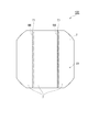
- the substrate 2 has a substantially square shape, and its four corners have an arc shape.
- One surface of the substrate 2 is a light receiving surface 21 and the other surface is a back surface 22 (see FIG. 2).
- the substrate 2 is made of at least one of, for example, Si single crystal, polycrystal, and amorphous.
- the substrate 2 may be an n-type semiconductor or a p-type semiconductor on the light receiving surface 21 side. For example, the distance between two opposing sides of the substrate 2 is 125 mm.
- a plurality of (for example, 48) linear finger electrodes 3 are disposed on the surface of the light receiving surface 21 so as to be spaced apart from each other in parallel.
- a TAB wire 4 is connected to the finger electrode 3 via a conductive adhesive film (conductive adhesive) 5 (see FIG. 4).
- the line width of the finger electrode 3 is, for example, 0.15 mm.
- An interval df between adjacent finger electrodes 3 is, for example, 2.55 mm.
- the finger electrode 3 is made of a known material capable of obtaining electrical continuity.
- the material of the finger electrode 3 includes a glass paste containing silver, a silver paste in which various conductive particles are dispersed in an adhesive resin, a gold paste, a carbon paste, a nickel paste, an aluminum paste, and ITO formed by firing or vapor deposition. Etc. Among these, it is preferable to use a glass paste containing silver from the viewpoint of heat resistance, conductivity, stability, and cost.
- the adhesion areas SF and SF indicate areas where the conductive adhesive films 5 and 5 are bonded on the light receiving surface 21.
- the width Wc (that is, the width of the conductive adhesive film 5) of the adhesive region SF is, for example, 1.2 mm.
- the distance dc between the adhesion areas SF, SF is, for example, 62 mm.
- the width of the TAB line 4 to be connected to the adhesion region SF is, for example, 1.5 mm.
- light receiving surface alignment marks (alignment marks) 6A and 6A are discontinuously provided along a line L intersecting the finger electrodes 3 and 3 located at both ends so as to form a broken line. . More specifically, the light receiving surface alignment mark 6 ⁇ / b> A has a pattern in which the portions 61 ⁇ / b> A intersecting with only one finger electrode 3 continue along the line L every other finger electrode 3. Yes.
- the light receiving surface alignment mark 6A indicates the connection position of the TAB line 4 with respect to the finger electrode 3, and is disposed, for example, at the center of the adhesion region SF.
- the light receiving surface alignment mark 6 ⁇ / b> A is integrally formed with the finger electrode 3 by the same material as the finger electrode 3. That is, the light receiving surface alignment mark 6A includes the above-described glass paste containing silver, silver paste in which various conductive particles are dispersed in an adhesive resin, gold paste, carbon paste, nickel paste, aluminum paste, and firing or vapor deposition. Among these, it is preferable to use a glass paste containing silver from the viewpoints of heat resistance, conductivity, stability, and cost.
- the light receiving surface alignment mark 6A is formed at the same time as the finger electrode 3 is formed.
- each portion 61A of the light-receiving surface alignment mark 6A is 0.05 mm or more and 0.2 mm or less, and for example, in this embodiment, it is 0.15 mm like the line width of the finger electrode 3. That is, each portion 61 ⁇ / b> A of the light receiving surface alignment mark 6 ⁇ / b> A has a line width equal to or smaller than the line width of the finger electrode 3.
- the line width of the light receiving surface alignment mark 6A is 0.05 mm or more, visibility can be secured, and the light receiving surface alignment mark 6A functions as an alignment mark. Further, when the line width of the light receiving surface alignment mark 6A is 0.2 mm or less, the usage amount of the electrode material can be sufficiently reduced.
- the light receiving surface alignment mark 6A has a line width equal to or smaller than the line width of the finger electrode 3, the amount of electrode material used can be further reduced.
- the line width of each portion 61A of the light receiving surface alignment mark 6A is preferably 20% or less of the line width of the TAB line to be connected.
- the interval between the light receiving surface alignment marks 6A and 6A is, for example, 62 mm, similarly to the interval dc between the adhesion regions SF and SF.
- the back surface electrode 7 is formed on the back surface 22 of the solar battery cell 100 so as to cover the entire surface.
- a TAB line 4 is connected to the back electrode 7 via a conductive adhesive film 5 (see FIG. 4).
- the back electrode 7 is formed, for example, by sintering aluminum paste.
- the adhesion areas SB and SB indicate areas where the conductive adhesive film 5 is adhered on the back surface 22, and are positions corresponding to the adhesion areas SF on the light receiving surface 21.
- the width of the adhesive region SB is, for example, 1.2 mm, similar to the width Wc (see FIG. 1) of the adhesive region SF.
- the distance between the adhesion areas SB and SB is, for example, about 62 mm, similar to the distance dc (see FIG. 1) between the adhesion areas SF and SF.
- the width of the TAB line 4 to be connected to the adhesive region SB is, for example, 1.5 mm, similarly to the width of the TAB line connected to the light receiving surface 21.
- the back surface 22 is provided with back surface alignment marks 71, 71 so as to connect two opposing sides of the substrate 2 along the adhesion region SB.
- This back surface alignment mark 71 shows the connection position of the TAB line 4 with respect to the back surface electrode 7, for example, is arrange
- the back surface alignment mark 71 has a groove shape, and the back surface alignment mark 71 allows the substrate 2 under the back surface electrode 7 to be exposed and visible.
- the width of the back surface alignment mark 71 is equal to or smaller than the width of the TAB line 4 and is, for example, about 0.1 to 0.9 mm.
- the distance between the back surface alignment marks 71 and 71 is, for example, 62 mm, similar to the distance between the adhesive regions SB and SB.
- such a solar battery cell 100 has a plurality of light receiving surface alignment marks 6A arranged in a line so that the light receiving surface alignment marks 6A are aligned, and the conductive adhesive film 5 along the light receiving surface alignment marks 6A.
- a TAB line 4 arranged via
- the finger electrode 3 on the light receiving surface 21 side of one solar cell 100A and the back electrode 7 on the back surface 22 side of the other solar cell 100B are connected to the TAB line 4.
- the finger electrode 3 on the light receiving surface 21 side of one solar cell 100B and the back surface on the back surface 22 side of the other solar cell 100C This is performed by connecting the electrode 7 to the TAB line and repeating this.
- positioned at 1 row is electrically connected in series.
- a solar cell module is formed by providing one or a plurality of such rows.
- the light receiving surface alignment marks 6A and 6A indicating the connection position of the TAB line 4 to the finger electrode 3 are on the lines L and L intersecting the finger electrodes 3 and 3 located at both ends. It is provided along. Therefore, the connection position of the TAB line 4 can be visually confirmed by checking the light receiving surface alignment marks 6A and 6A, and the TAB line 4 can be connected to the planned position with high accuracy.
- the light receiving surface alignment mark 6 ⁇ / b> A is integrally formed at the same time as the finger electrode 3 with the same material as the finger electrode 3 when the finger electrode 3 is formed. For this reason, the light-receiving surface alignment mark 6A can be formed easily, and an increase in manufacturing cost can be suppressed.
- the light receiving surface alignment mark 6A is formed discontinuously along the line L and has a line width equal to or smaller than the line width of the TAB line 4 to be connected. Therefore, an increase in the amount of electrode material used can be suppressed as compared with a conventional solar battery cell in which continuous bus bar electrodes having the same width as the TAB line are formed. Therefore, an increase in manufacturing cost can be suppressed.
- the light receiving surface alignment mark 6A has a broken line shape, so that it is possible to achieve both suppression of the amount of electrode material used and visibility.
- each portion 61A of the light receiving surface alignment mark 6A has a line width of 0.05 mm or more and 0.2 mm or less, and by extension, a line width of the finger electrode 3 or less.
- the increase in the usage amount can be further suppressed, and the increase in manufacturing cost can be suppressed.
- a plurality of solar cells 100 are arranged and formed on the finger electrodes 3 of one adjacent solar cell 100 and the back surface 22 of the other solar cell 100.
- the back electrode 7 is connected by a TAB line 4 disposed via the conductive adhesive film 5 along the light receiving surface alignment mark 6A.
- the TAB line 4 is accurately connected to the planned position, it is possible to suppress meandering of the rows of solar cells 100. Thereby, when manufacturing a solar cell module, it can suppress that a residual stress generate
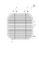
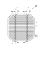
- FIG. 5 is a plan view showing the surface of the solar battery cell according to the second embodiment of the present invention.
- the solar cell 110 according to this embodiment is different from the solar cell 100 according to the first embodiment (see FIG. 1) in that the arrangement pattern of the part constituting the alignment mark is the light receiving surface alignment.
- the light-receiving surface alignment mark 6B different from the mark 6A is provided.
- the light receiving surface alignment mark 6B has a pattern in which a portion 61B straddling two finger electrodes 3 and 3 that are adjacent to each other is continuous along the line L.
- each part 61B of the light receiving surface alignment mark 6B extends over the two finger electrodes 3 and 3.
- the light receiving surface alignment mark 6 ⁇ / b> B having such a configuration contributes to simplification of inspection such as disconnection of the finger electrode 3. That is, in such a configuration, since the plurality of finger electrodes 3 over which the respective portions 61B are strung are formed as one lump, the plurality of finger electrodes 3 can be inspected at a time by contact with the inspection stylus. Therefore, the number of styluses required for the inspection can be reduced, and the cost for the inspection can be reduced.
- FIG. 6 is a plan view showing the surface of the solar battery cell according to the third embodiment of the present invention.
- the solar battery cell 120 according to the present embodiment is different from the solar battery cell 100 according to the first embodiment (see FIG. 1) in that the arrangement pattern of the part constituting the alignment mark is the light receiving surface alignment. This is that a light receiving surface alignment mark 6C different from the mark 6A is provided.
- the light receiving surface alignment mark 6C includes a portion 61C intersecting with only one finger electrode 3 and a portion 62C straddling the two adjacent finger electrodes 3 and 3 in a line L.
- the pattern is alternately continuous along. Further, the portions 62C and 62C are positioned outside the finger electrodes 3 and 3 located at both ends, and the portions 62C and 62C are connected to only one finger electrode 3 here.
- each portion 62C of the light receiving surface alignment mark 6C extends over the two finger electrodes 3 and 3.
- the light receiving surface alignment mark 6 ⁇ / b> C having such a configuration contributes to simplification of inspection such as disconnection of the finger electrode 3. That is, in such a configuration, since the plurality of finger electrodes 3 over which the respective parts 62C are strung constitute a single lump, the plurality of finger electrodes 3 can be inspected at a time by contact with a probe for inspection. Therefore, the number of styluses required for the inspection can be reduced, and the cost for the inspection can be reduced.
- the parts 62C and 62C are located outside the finger electrodes 3 and 3 located at both ends, when the conductive adhesive film 5 is adhered to the photovoltaic cell 120, the conductive adhesion is performed.
- the portions 62C and 62C of the light receiving surface alignment mark 6C can be protruded outside the film 5. Thereby, it can be visually recognized whether or not the conductive adhesive film 5 is adhered to the planned position, and the TAB wire 4 can be connected to the planned position with higher accuracy.
- FIG. 7 is a plan view showing the surface of the solar battery cell according to the fourth embodiment of the present invention.
- the solar battery cell 130 according to the present embodiment is different from the solar battery cell 100 according to the first embodiment (see FIG. 1) in that the arrangement pattern of the part constituting the alignment mark is the light receiving surface alignment. This is that a light receiving surface alignment mark 6D different from the mark 6A is provided.
- the light receiving surface alignment mark 6D has a pattern in which a portion 61D straddling two adjacent finger electrodes 3 and 3 is continuous along the line L so as to connect the two finger electrodes 3 and 3 to each other. Further, the portions 61D and 61D are located outside the finger electrodes 3 and 3 located at both ends, and the portions 61D and 61D are each connected to only one finger electrode 3 here.
- each portion 61D of the light receiving surface alignment mark 6D extends over the two finger electrodes 3 and 3.
- the light receiving surface alignment mark 6 ⁇ / b> D having such a configuration contributes to simplification of inspection such as disconnection of the finger electrode 3. That is, in such a configuration, since the plurality of finger electrodes 3 over which the respective portions 61D are strung are formed as one lump, the plurality of finger electrodes 3 can be inspected at a time by contact with the inspection stylus. Therefore, the number of styluses required for the inspection can be reduced, and the cost for the inspection can be reduced.
- the parts 61D and 61D are located outside the finger electrodes 3 and 3 located at both ends, when the conductive adhesive film 5 is adhered to the photovoltaic cell 130, the conductive adhesion is performed.
- the portions 61D and 61D of the light receiving surface alignment mark 6D can be protruded outside the film 5. Thereby, it can be visually recognized whether or not the conductive adhesive film 5 is adhered to the planned position, and the TAB wire 4 can be connected to the planned position with higher accuracy.
- FIG. 8 is a plan view showing the surface of the solar battery cell according to the fifth embodiment of the present invention.
- the solar cell 140 according to the present embodiment is different from the solar cell 100 according to the first embodiment (see FIG. 1) in that the length of the portion constituting the alignment mark and the arrangement pattern Is that a light receiving surface alignment mark 6E different from the light receiving surface alignment mark 6A is provided.
- the light receiving surface alignment mark 6E has a pattern in which a portion 61E extending across the finger electrodes 3 and 3 at both ends of the four adjacent finger electrodes 3 to 3 continues along the line L. .
- a portion 61D intersecting with the finger electrode 3 located at the lower end extends over only the three adjacent finger electrodes 3 to 3.
- one finger electrode 3 that is not connected to the portion 61E is interposed between the continuous portions 61E and 61E.
- each portion 61E of the light receiving surface alignment mark 6E extends over the four finger electrodes 3 and 3.
- the light receiving surface alignment mark 6 ⁇ / b> E having such a configuration contributes to simplification of inspection such as disconnection of the finger electrode 3. That is, in such a configuration, since the plurality of finger electrodes 3 over which the respective portions 61E are strung constitute a single lump, the plurality of finger electrodes 3 can be inspected at a time by contact with the inspection stylus. Therefore, the number of styluses required for the inspection can be reduced, and the cost for the inspection can be reduced.
- FIG. 9 is a plan view showing the surface of the solar battery cell according to the sixth embodiment of the present invention.
- the solar battery cell 150 according to the present embodiment is different from the solar battery cell 100 according to the first embodiment (see FIG. 1) in that the length of the part constituting the alignment mark and the arrangement pattern Is that a light receiving surface alignment mark 6F different from the light receiving surface alignment mark 6A is provided.
- the light receiving surface alignment mark 6F has a pattern in which a portion 61F extending over the three adjacent finger electrodes 3 to 3 so as to intersect with each other is continuous along the line L.
- One finger electrode 3 not connected to the portion 61F is interposed between the continuous portions 61F and 61F.
- each portion 61F of the light receiving surface alignment mark 6F extends over the three finger electrodes 3 to 3.
- the light receiving surface alignment mark 6 ⁇ / b> F having such a configuration contributes to simplification of inspection such as disconnection of the finger electrode 3.
- the plurality of finger electrodes 3 over which the respective portions 61F are stretched are formed as one lump, so that the plurality of finger electrodes 3 can be inspected at a time by contact with a probe for inspection. Therefore, the number of styluses required for the inspection can be reduced, and the cost for the inspection can be reduced.
- FIG. 10 is a plan view showing the surface of the solar battery cell according to the seventh embodiment of the present invention.
- the solar cell 160 according to this embodiment is different from the solar cell 100 according to the first embodiment (see FIG. 1) in that the length of the portion constituting the alignment mark and the arrangement pattern Is that a light receiving surface alignment mark 6G different from the light receiving surface alignment mark 6A is provided.
- the light receiving surface alignment mark 6G has a pattern in which a portion 61G spanning the finger electrodes 3 and 3 at both ends of the adjacent three finger electrodes 3 to 3 is continuous along the line L. .
- the lower end of the portion 61G protrudes between the three adjacent finger electrodes 3 to 3.
- two finger electrodes 3 that are not connected to the portion 61G are interposed between the continuous portions 61G and 61G.
- each part 61G of the light receiving surface alignment mark 6G extends over the three finger electrodes 3 to 3.
- the light receiving surface alignment mark 6G having such a configuration contributes to simplification of inspection such as disconnection of the finger electrode 3. That is, in such a configuration, since the plurality of finger electrodes 3 over which the respective portions 61G are strung are formed as one lump, the plurality of finger electrodes 3 can be inspected at a time by contact with a probe for inspection. Therefore, the number of styluses required for the inspection can be reduced, and the cost for the inspection can be reduced.
- FIG. 11 is a plan view showing the surface of the solar battery cell according to the eighth embodiment of the present invention.
- the solar cell 170 according to the present embodiment is different from the solar cell 100 according to the first embodiment (see FIG. 1) in that the length of the portion constituting the alignment mark and the arrangement pattern Is that a light receiving surface alignment mark 6H different from the light receiving surface alignment mark 6A is provided.
- the light-receiving surface alignment mark 6H extends across the finger electrodes 3 and 3 at both ends of the adjacent three finger electrodes 3 to 3 so that the lower end protrudes from between the three finger electrodes 3 to 3.
- a portion 61H extending between the three finger electrodes 3 to 3 so as to connect the portion 61H to the finger electrodes 3 and 3 at both ends of the adjacent three finger electrodes 3 to 3 62H is a pattern that continues alternately along the line L.
- the finger electrode 3 which is not connected with the part 61H and the part 62H is interposed.
- each of the portions 61H and 62H of the light receiving surface alignment mark 6H extends over the three finger electrodes 3 to 3.
- the light receiving surface alignment mark 6 ⁇ / b> H having such a configuration contributes to simplification of inspection such as disconnection of the finger electrode 3. That is, in such a configuration, since the plurality of finger electrodes 3 each spanning each of the portions 61H and 62H form one lump, the plurality of finger electrodes 3 can be inspected at a time by contact with the stylus for inspection. . Therefore, the number of styluses required for the inspection can be reduced, and the cost for the inspection can be reduced.
- FIG. 12 is a plan view showing the surface of the solar battery cell according to the ninth embodiment of the present invention.
- the solar cell 180 according to this embodiment is different from the solar cell 100 according to the first embodiment (see FIG. 1) in that the light receiving surface alignment mark 6I is for one line L. This is a point in which a plurality are provided.
- a plurality of (for example, two) light receiving surface alignment marks 6I are provided for one line L.
- the light receiving surface alignment marks 6I are provided on the left and right with the one line L as the center.
- the width Wa of the light receiving surface alignment marks 6I and 6I is equal to or larger than the width of the adhesive region SF (that is, the width of the conductive adhesive film 5).
- the light receiving surface alignment mark 6 ⁇ / b> I has a pattern in which the portions 61 ⁇ / b> I intersecting with only one finger electrode 3 are continuous along the line L every other finger electrode 3.
- the respective portions 61I are provided alternately on the left and right, so that the light receiving surface alignment marks 6I and 6I form a staggered pattern. Yes.
- the light-receiving surface alignment mark 6I is provided with two (for example, two) with respect to the one line L, the visibility of an alignment mark improves and the TAB line
- the width Wa of the light receiving surface alignment marks 6I and 6I provided for a plurality of (for example, two) one line L is equal to or larger than the width Wc of the conductive adhesive film 5. Therefore, by adhering the conductive adhesive film 5 between the light receiving surface alignment marks 6I and 6I, the light receiving surface alignment marks 6I and 6I can be visually recognized after the conductive adhesive film 5 is bonded. Therefore, the TAB line 4 can be connected to a predetermined position with higher accuracy.
- the photovoltaic cell 180 since the light receiving surface alignment marks 6I and 6I provided with respect to one line L are staggered, the visibility of the alignment mark is further improved, and the TAB line 4 is It is possible to connect to a predetermined position with high accuracy.
- FIG. 13 is a plan view showing the surface of the solar battery cell according to the tenth embodiment of the present invention.
- the solar cell 190 according to the present embodiment is different from the solar cell 100 according to the first embodiment (see FIG. 1) in that the arrangement pattern of the part constituting the alignment mark is the light receiving surface alignment.
- This is that a plurality of light receiving surface alignment marks 6J different from the mark 6A are provided for one line L.
- a plurality of (for example, two) light receiving surface alignment marks 6J are provided for one line L.
- the light receiving surface alignment marks 6J are provided on the left and right sides of the one line L.
- the width Wa of the light receiving surface alignment marks 6J, 6J is equal to or greater than the width of the adhesive region SF (that is, the width of the conductive adhesive film 5) Wc.
- the light receiving surface alignment mark 6J has a pattern in which a portion 61J straddling two finger electrodes 3 and 3 that are adjacent to each other is continuous along the line L.
- the portions 61J are provided alternately on the left and right, so that the light receiving surface alignment marks 6J and 6J are staggered. Yes. Further, since the portions 61J straddling the two adjacent finger electrodes 3 and 3 are arranged in a staggered manner, all the finger electrodes 3 are connected by the light receiving surface alignment marks 6J and 6J.
- the photovoltaic cell 190 since multiple light receiving surface alignment marks 6J are provided for one line L (for example, two), the visibility of the alignment marks is improved, and the TAB line 4 is scheduled. Can be accurately connected to the desired position.
- the width Wa of the light receiving surface alignment marks 6 ⁇ / b> J and 6 ⁇ / b> J provided for a plurality of (for example, two) one line L is equal to or larger than the width Wc of the conductive adhesive film 5. Therefore, by adhering the conductive adhesive film 5 between the light receiving surface alignment marks 6J and 6J, the light receiving surface alignment marks 6J and 6J can be visually recognized after the conductive adhesive film 5 is bonded. Therefore, the TAB line 4 can be connected to a predetermined position with higher accuracy.
- the photovoltaic cell 190 since the light-receiving surface alignment marks 6J and 6J provided with respect to one line L are staggered, the visibility of the alignment marks is further improved, and the TAB line 4 is It is possible to connect to a predetermined position with high accuracy.
- the part 61J which straddles two adjacent finger electrodes 3 and 3 is arrange
- all the finger electrodes 3 are connected by the light-receiving surface alignment mark 6J and 6J.
- the light receiving surface alignment mark 6J having such a configuration contributes to simplification of inspection such as disconnection of the finger electrode 3. That is, in such a configuration, all the finger electrodes 3 form one lump, so that all the finger electrodes 3 can be inspected at once by contact with the inspection stylus. Therefore, the number of styluses required for the inspection can be reduced, and the cost for the inspection can be reduced.
- FIG. 14 is a plan view showing the surface of the solar battery cell according to the eleventh embodiment of the present invention.
- the solar cell 200 according to the present embodiment is different from the solar cell 100 according to the first embodiment (see FIG. 1) in that the arrangement pattern of the part constituting the alignment mark is the light receiving surface alignment.
- This is that a plurality of light receiving surface alignment marks 6K different from the mark 6A are provided for one line L.
- a plurality of (for example, two) light receiving surface alignment marks 6K are provided for one line L.
- the light receiving surface alignment marks 6K are provided on the left and right sides with respect to one line L.
- the width Wa of the light receiving surface alignment marks 6K, 6K is equal to or greater than the width of the adhesive region SF (that is, the width of the conductive adhesive film 5) Wc.
- the light receiving surface alignment mark 6K includes a portion 61K that intersects only one finger electrode 3 and a portion 62K that straddles the two adjacent finger electrodes 3 and 3 along the line L. The pattern is alternately continuous.
- each portion 62K of the light receiving surface alignment mark 6K extends over the two finger electrodes 3 and 3.
- the light receiving surface alignment mark 6 ⁇ / b> K having such a configuration contributes to simplification of inspection such as disconnection of the finger electrode 3. That is, in such a configuration, since the plurality of finger electrodes 3 over which the respective parts 62K are straddled become one lump, the plurality of finger electrodes 3 can be inspected at a time by contact with a probe for inspection. Therefore, the number of styluses required for the inspection can be reduced, and the cost for the inspection can be reduced.
- the light-receiving surface alignment mark 6K is provided with two or more (for example, two) with respect to the one line L, the visibility of the alignment mark improves and the TAB line 4 is scheduled. Can be accurately connected to the desired position.
- the width Wa of the light receiving surface alignment marks 6K, 6K provided in a plurality (for example, two) for one line L is equal to or larger than the width Wc of the conductive adhesive film 5. Therefore, by adhering the conductive adhesive film 5 between the light receiving surface alignment marks 6K and 6K, the light receiving surface alignment marks 6K and 6K can be visually recognized after the conductive adhesive film 5 is bonded. Therefore, the TAB line 4 can be connected to a predetermined position with higher accuracy.
- FIG. 15 is a plan view showing the surface of the solar battery cell according to the twelfth embodiment of the present invention.
- the solar cell 210 according to the present embodiment is different from the solar cell 100 according to the first embodiment (see FIG. 1) in that the arrangement pattern of the part constituting the alignment mark is the light receiving surface alignment. This is that a plurality of light receiving surface alignment marks 6L different from the mark 6A are provided for one line L.
- a plurality of (for example, two) light receiving surface alignment marks 6L are provided for one line L.
- the light receiving surface alignment marks 6L are provided on the left and right sides with respect to one line L.
- the width Wa of the light receiving surface alignment marks 6L, 6L is equal to or greater than the width of the adhesive region SF (that is, the width of the conductive adhesive film 5) Wc.
- the light receiving surface alignment mark 6 ⁇ / b> L has a pattern in which a portion 61 ⁇ / b> L straddling the two adjacent finger electrodes 3 and 3 is continuous along the line L.
- the portions 61L are alternately provided on the left and right, so that the light receiving surface alignment marks 6L and 6L are staggered. Yes. Further, since the portions 61L straddling the two adjacent finger electrodes 3 and 3 are arranged in a staggered manner, all the finger electrodes 3 are connected by the light receiving surface alignment marks 6L and 6L.
- the light-receiving surface alignment mark 6L is provided with two or more (for example, two) with respect to the one line L, the visibility of an alignment mark improves and the TAB line
- the width Wa of the light receiving surface alignment marks 6 ⁇ / b> L and 6 ⁇ / b> L provided for a plurality of (for example, two) one line L is equal to or larger than the width Wc of the conductive adhesive film 5. Therefore, by adhering the conductive adhesive film 5 between the light receiving surface alignment marks 6L and 6L, the light receiving surface alignment marks 6L and 6L can be visually recognized after the conductive adhesive film 5 is bonded. Therefore, the TAB line 4 can be connected to a predetermined position with higher accuracy.
- the photovoltaic cell 210 since the light-receiving surface alignment marks 6L and 6L provided with respect to one line L are staggered, the visibility of the alignment marks is further improved, and the TAB line 4 is It is possible to connect to a predetermined position with high accuracy.
- the part 61L which straddles two adjacent finger electrodes 3 and 3 is arrange
- all the finger electrodes 3 are connected by the light-receiving surface alignment marks 6L and 6L.
- the light receiving surface alignment mark 6 ⁇ / b> L having such a configuration contributes to simplification of inspection such as disconnection of the finger electrode 3. That is, in such a configuration, all the finger electrodes 3 form one lump, so that all the finger electrodes 3 can be inspected at once by contact with the inspection stylus. Therefore, the number of styluses required for the inspection can be reduced, and the cost for the inspection can be reduced.
- FIG. 16 is a plan view showing the surface of the solar battery cell according to the thirteenth embodiment of the present invention.
- the solar cell 220 according to the present embodiment is different from the solar cell 100 according to the first embodiment (see FIG. 1) in that the arrangement pattern of the part constituting the alignment mark is the light receiving surface alignment.
- the light receiving surface alignment marks 6M and 6N different from the mark 6A are provided for one line L.
- the light receiving surface alignment marks 6M and 6N are provided for one line L, for example, left and right with the one line L as the center.
- the width Wa of the light receiving surface alignment marks 6M and 6N is equal to or larger than the width of the adhesive region SF (that is, the width of the conductive adhesive film 5).
- the light receiving surface alignment mark 6M has a pattern in which a portion 61M straddling the finger electrodes 3 and 3 on both ends of the four adjacent finger electrodes 3 to 3 is continuous along the line L. .
- One finger electrode 3 not connected to the portion 61M is interposed between the continuous portions 61M and 61M.
- the light receiving surface alignment mark 6N has a pattern in which a portion 61N extending across the finger electrodes 3 and 3 at both ends of the adjacent three finger electrodes 3 to 3 is continuous along the line L. . Two finger electrodes 3 not connected to the portion 61N are interposed between the continuous portions 61N and 61N. Further, in the light receiving surface alignment marks 6M, 6N provided on the left and right with the line L as the center, the portions 61M, 61N are provided alternately on the left and right, so that the light receiving surface alignment marks 6M, 6N are staggered. There is no. Further, since the portions 61M and 61N extending over the plurality of finger electrodes 3 to 3 are arranged in a staggered manner, all the finger electrodes 3 are connected by the light receiving surface alignment marks 6M and 6N.
- the plurality of light receiving surface alignment marks 6M and 6N are provided for one line L, the visibility of the alignment mark is improved and the TAB line 4 is placed at a predetermined position. Connection can be made with high accuracy.
- the width Wa of the light receiving surface alignment marks 6M and 6N provided for one line L is equal to or larger than the width Wc of the conductive adhesive film 5, the light receiving surface alignment mark
- the TAB line 4 can be connected to a predetermined position with higher accuracy.
- the light-receiving surface alignment marks 6M and 6N provided with respect to one line L are staggered, the visibility of the alignment marks is further improved, and the TAB line 4 is scheduled. It is possible to connect to the specified position with high accuracy.
- the portions 61M and 61N straddling a plurality of adjacent finger electrodes 3 are arranged in a staggered manner, so that all the finger electrodes 3 are connected by the light receiving surface alignment marks 6M and 6N. ing.
- the light receiving surface alignment marks 6M and 6N having such a configuration contribute to simplification of inspection such as disconnection of the finger electrode 3. That is, in such a configuration, all the finger electrodes 3 form one lump, so that all the finger electrodes 3 can be inspected at once by contact with the inspection stylus. Therefore, the number of styluses required for the inspection can be reduced, and the cost for the inspection can be reduced.
- FIG. 17 is a plan view showing the surface of the solar battery cell according to the fourteenth embodiment of the present invention.
- the solar cell 230 according to the present embodiment is different from the solar cell 100 according to the first embodiment (see FIG. 1) in that the arrangement pattern of the part constituting the alignment mark is the light receiving surface alignment. This is that a plurality of light receiving surface alignment marks 60 different from the mark 6A are provided for one line L.
- a plurality of (for example, two) light receiving surface alignment marks 6O are provided for one line L, and are provided, for example, on the left and right with one line L as the center.
- the width Wa of the light receiving surface alignment marks 6O, 6O is equal to or larger than the width of the adhesive region SF (that is, the width of the conductive adhesive film 5) Wc.
- the light receiving surface alignment mark 6O has a pattern in which a portion 61O extending across the three finger electrodes 3 to 3 adjacent to each other is continuous along the line L. One finger electrode 3 that is not connected to the portion 61O is interposed between the continuous portions 61O and 61O.
- the portions 61O are provided alternately on the left and right, so that the light receiving surface alignment marks 6O, 6O are staggered. Yes. Further, since the portions 61O straddling the three adjacent finger electrodes 3 to 3 are arranged in a staggered manner, all the finger electrodes 3 are connected by the light receiving surface alignment marks 6O and 6O.
- the solar battery 230 since a plurality of (for example, two) light receiving surface alignment marks 60 are provided for one line L, the visibility of the alignment marks is improved, and the TAB line 4 is scheduled. Can be accurately connected to the desired position.
- the width Wa of the light receiving surface alignment marks 6 ⁇ / b> O and 6 ⁇ / b> O provided for a plurality of (for example, two) one line L is equal to or larger than the width Wc of the conductive adhesive film 5. Therefore, by adhering the conductive adhesive film 5 between the light receiving surface alignment marks 6O and 6O, the light receiving surface alignment marks 6O and 6O can be visually recognized after the conductive adhesive film 5 is bonded. Therefore, the TAB line 4 can be connected to a predetermined position with higher accuracy.
- the photovoltaic cell 230 since the light-receiving surface alignment marks 6O and 6O provided with respect to one line L are staggered, the visibility of the alignment marks is further improved, and the TAB line 4 is It is possible to connect to a predetermined position with high accuracy.
- the portions 61O straddling the three adjacent finger electrodes 3 to 3 are arranged in a staggered manner, all the finger electrodes 3 are connected by the light receiving surface alignment marks 6O and 6O.
- the light-receiving surface alignment mark 60 having such a configuration contributes to simplification of inspection such as disconnection of the finger electrode 3. That is, in such a configuration, all the finger electrodes 3 form one lump, so that all the finger electrodes 3 can be inspected at once by contact with the inspection stylus. Therefore, the number of styluses required for the inspection can be reduced, and the cost for the inspection can be reduced.
- FIG. 18 is a plan view showing the surface of the solar battery cell according to the fifteenth embodiment of the present invention.
- the solar cell 240 according to the present embodiment is different from the solar cell 100 according to the first embodiment (see FIG. 1) in that the arrangement pattern of the portion constituting the alignment mark is the light receiving surface alignment. This is that a plurality of light receiving surface alignment marks 6P different from the mark 6A are provided for one line L.
- a plurality of (for example, two) light receiving surface alignment marks 6P are provided for one line L.
- the light receiving surface alignment marks 6P are provided on the left and right sides of the one line L.
- the width Wa of the light receiving surface alignment marks 6P, 6P is equal to or greater than the width of the adhesive region SF (that is, the width of the conductive adhesive film 5) Wc.
- the light receiving surface alignment mark 6P has a pattern in which a portion 61P that extends across the finger electrodes 3 and 3 at both ends of the three adjacent finger electrodes 3 to 3 is continuous along the line L. Yes.
- One finger electrode 3 that is not connected to the portion 61P is interposed between the continuous portions 61P and 61P.
- the portions 61P are provided alternately on the left and right, so that the light receiving surface alignment marks 6P and 6P are staggered. Yes. Further, the portions 61P straddling the three adjacent finger electrodes 3 to 3 are arranged in a staggered manner, so that all the finger electrodes 3 are connected by the light receiving surface alignment marks 6P and 6P.
- the light-receiving surface alignment mark 6P is provided with two or more (for example, two) with respect to one line L, the visibility of the alignment mark is improved and the TAB line 4 is scheduled. Can be accurately connected to the desired position.
- the width Wa of the light receiving surface alignment marks 6 ⁇ / b> P, 6 ⁇ / b> P provided for a plurality of (for example, two) one line L is equal to or larger than the width Wc of the conductive adhesive film 5. Therefore, by adhering the conductive adhesive film 5 between the light receiving surface alignment marks 6P and 6P, the light receiving surface alignment marks 6P and 6P can be visually recognized after the conductive adhesive film 5 is bonded. Therefore, the TAB line 4 can be connected to a predetermined position with higher accuracy.
- the photovoltaic cell 240 since the light-receiving surface alignment marks 6P and 6P provided with respect to one line L are staggered, the visibility of the alignment marks is further improved, and the TAB line 4 is It is possible to connect to a predetermined position with high accuracy.
- the portions 61P straddling the three adjacent finger electrodes 3 to 3 are arranged in a staggered manner, so that all the finger electrodes 3 are connected by the light receiving surface alignment marks 6P and 6P.
- the light receiving surface alignment mark 6 ⁇ / b> P having such a configuration contributes to simplification of inspection such as disconnection of the finger electrode 3. That is, in such a configuration, all the finger electrodes 3 form one lump, so that all the finger electrodes 3 can be inspected at once by contact with the inspection stylus. Therefore, the number of styluses required for the inspection can be reduced, and the cost for the inspection can be reduced.
- FIG. 19 is a plan view showing the surface of the solar battery cell according to the sixteenth embodiment of the present invention.
- the solar battery cell 250 according to the present embodiment is different from the solar battery cell 100 according to the first embodiment (see FIG. 1) in that the arrangement pattern of the part constituting the alignment mark is the light receiving surface alignment.
- the light receiving surface alignment marks 6Q and 6R different from the mark 6A are provided for one line L.
- the light receiving surface alignment marks 6Q and 6R are provided for one line L, for example, left and right around the one line L.
- the width Wa of the light receiving surface alignment marks 6Q and 6R is equal to or greater than the width of the adhesive region SF (that is, the width of the conductive adhesive film 5).
- the light receiving surface alignment mark 6Q has a pattern in which a portion 61Q extending over the three finger electrodes 3 to 3 adjacent to each other so as to intersect with each other is continuous along the line L. Two finger electrodes 3 not connected to the portion 61Q are interposed between the continuous portions 61Q and 61Q.
- the light receiving surface alignment mark 6R has a pattern in which a portion 61R straddling the finger electrodes 3 and 3 at both ends of the four adjacent finger electrodes 3 to 3 is continuous along the line L. .
- One finger electrode 3 not connected to the portion 61R is interposed between the continuous portions 61R and 61R.
- the portions 61Q and 61R are provided alternately on the left and right, so that the light receiving surface alignment marks 6Q and 6R are staggered. There is no. Further, since the portions 61Q and 61R straddling the plurality of finger electrodes 3 to 3 are arranged in a staggered manner, all the finger electrodes 3 are connected by the light receiving surface alignment marks 6Q and 6R.
- the plurality of light receiving surface alignment marks 6Q and 6R are provided for one line L, the visibility of the alignment mark is improved, and the TAB line 4 is placed at a predetermined position. Connection can be made with high accuracy.
- the width Wa of the light receiving surface alignment marks 6Q and 6R provided with respect to one line L is equal to or larger than the width Wc of the conductive adhesive film 5, the light receiving surface alignment marks.
- the TAB line 4 can be connected to a predetermined position with higher accuracy.
- the light receiving surface alignment marks 6Q and 6R provided for a single line L are staggered, the visibility of the alignment marks is further improved, and the TAB line 4 is planned. It is possible to connect to the specified position with high accuracy.
- the parts 61Q and 61R straddling a plurality of adjacent finger electrodes 3 are arranged in a staggered manner, all the finger electrodes 3 are connected by the light receiving surface alignment marks 6Q and 6R. ing.
- the light receiving surface alignment marks 6Q and 6R having such a configuration contribute to simplification of inspection such as disconnection of the finger electrode 3. That is, in such a configuration, all the finger electrodes 3 form one lump, so that all the finger electrodes 3 can be inspected at once by contact with the inspection stylus. Therefore, the number of styluses required for the inspection can be reduced, and the cost for the inspection can be reduced.
- FIG. 20 is a plan view showing the surface of the solar battery cell according to the seventeenth embodiment of the present invention.
- the solar cell 260 according to the present embodiment is different from the solar cell 100 according to the first embodiment (see FIG. 1) in that the finger electrode 3 located at the end and the finger electrode 3 are different.
- a point is that a portion 61S connecting adjacent finger electrodes 3 is provided with a light receiving surface alignment mark 6S provided at both ends.
- the photovoltaic cell 260 since the light-receiving surface alignment mark 6S consists of the part 61S which ties the finger electrode 3 located in the end, and the finger electrode 3 adjacent to this finger electrode 3, the usage-amount of electrode material An increase can be further suppressed, and an increase in manufacturing cost can be suppressed.
- the back electrode 7 and the TAB line 4 are connected via the conductive adhesive film 5, but a bus bar electrode made of Ag or the like at the position where the TAB line 4 on the back electrode 7 is connected. And the back electrode 7 and the TAB line 4 may be electrically connected by connecting the bus bar electrode and the TAB line 4 with solder.
- the film-like conductive adhesive film 5 is used as the conductive adhesive, but a liquid conductive adhesive may be applied.
- the light receiving surface alignment mark may be formed of a material different from that of the finger electrodes.
- a material of the light receiving surface alignment mark in the above embodiment for example, by using a material that is cheaper than the material of the finger electrode, the manufacturing cost can be reduced.
- different materials include materials having different composition components in the materials and materials having the same composition components but different contents.
- the light receiving surface alignment mark 6T shown in FIG. 21 has a broken line shape, and a pattern in which the portions 61T and the portions 62T whose length along the line L is shorter than the portion 61T is alternately continuous. Yes. A plurality of portions 61T may be continued, or a plurality of portions 62T may be continued.
- the solar cell in particular, a single crystal silicon substrate, a polycrystalline silicon substrate, or a single crystal silicon laminated amorphous silicon substrate is used.
- a single crystal silicon substrate for example, HIT series manufactured by Panasonic Corporation.
- the glass paste containing aluminum other than the above-mentioned material the glass paste containing copper, the alloy containing at least one among silver, aluminum, copper is contained. Glass paste and the like. The same applies to the material of the light receiving surface alignment mark in the above embodiment.
- the line width of each part of the light receiving surface alignment mark is more preferably 0.10 mm or more and 0.18 mm or less.
- the number of adhesion regions SF (the number of TAB lines) is two, but other numbers (for example, 3 to 5) may be used.
- the number of finger electrodes at which each portion of the light receiving surface alignment mark intersects is preferably 2 or more, more preferably 2 or more and 20 or less, and particularly preferably 2 or more and 10 or less.
- the number of finger electrodes at which the respective portions of the light receiving surface alignment mark intersect does not have to be the same in all the portions, and may be different for each portion.
- the finger electrodes need not be linear.
Landscapes
- Photovoltaic Devices (AREA)
Abstract
太陽電池セルであって、基板の受光面に配置された複数のフィンガー電極と、フィンガー電極に対して接着剤を介してTAB線が接着される位置を示すアライメントマークと、を備え、アライメントマークは、受光面の対向する端部の最も近くに位置する二つのフィンガー電極と交差するラインに沿って、受光面に不連続に設けられた部分を有する。
Description
本発明は、太陽電池セル、太陽電池モジュール、太陽電池セルの製造方法及び太陽電池モジュールの製造方法に関する。
近年、深刻化する地球温暖化や化石エネルギー枯渇問題を解決する手段として、太陽電池が注目されている。この太陽電池は、通常、複数の太陽電池セルを直列又は並列に接続することで形成される。この太陽電池セルの表面(受光面)には、出力を得るためのAgからなる直線状の電極(フィンガー電極)が、互いに平行に複数本形成されている。また、裏面には、その全面を覆うようにAlからなる裏面電極が形成されている。そして、隣接する太陽電池セルのうち、一方の太陽電池セルの受光面に全てのフィンガー電極と互いに直交するように金属配線部材(TAB線)を接続し、さらにこのTAB線を他方の太陽電池セルの裏面電極に接続することで、隣接する太陽電池セルが互いに接続される。
従来、TAB線の接続には、良好な導電性を示すはんだが使用されてきた(特許文献1)。また、最近では、環境問題を考慮して、Pbを含まないSn-Ag-Cuはんだが使用されることもある(特許文献1、2)。しかし、これらのはんだをTAB線の接続に使用する場合、約220℃以上の熱が太陽電池セルに加わるため、接続工程の歩留りの低下や太陽電池セルの反りが発生するおそれがある。これらを抑制するために、太陽電池セル中のシリコンの厚みを増加させることが考えられる。しかし、この場合、製造コストが増加してしまう。
また、上記のようなはんだをTAB線の接続に使用する場合、はんだのぬれ性を確保するために、太陽電池セルの表面及び裏面において当該TAB線が配置される位置に、予めAgからなる電極(バスバー電極)を形成しておく必要がある。しかし、Agは高価であるため、製造コストが増加してしまう。また、Agの電気抵抗は大きいため、バスバー電極が細いと、当該バスバー電極のシート抵抗が大きくなる。そうすると、バスバー電極における電力損失が増加して、太陽電池セルの発電性能が低下してしまう。このため、バスバー電極のシート抵抗を抑制するために、バスバー電極の幅はある程度太くする必要があり、さらに製造コストが増加する原因となっている。
そこで、近年、はんだに代えて導電性接着層を有する導電性接着剤をTAB線の接続に使用することが提案されている(特許文献3~6)。この導電性接着剤は熱硬化性樹脂中にAl粒子等の金属粒子を混合・分散させた組成物であり、この金属粒子がTAB線と太陽電池セルの電極との間に挟まれることで電気的な接続が実現される。導電性接着剤をTAB線の接続に使用する場合、200℃以下で接続を行うことが可能であるため、接続工程の歩留りの低下や太陽電池セルの反りが抑制される。また、導電性接着剤をTAB線の接続に使用する場合、ぬれ性の確保が不要となるため、ぬれ性の確保のために形成されていたバスバー電極が不要となり、Agの使用が低減される。
しかしながら、太陽電池セルの表面及び裏面にバスバー電極が形成されていないと、TAB線の接続位置が確認できず、TAB線を予定された位置に精度良く貼り付けることができないおそれがある。TAB線を予定された位置に貼り付けることができないと、太陽電池セルの並びが蛇行してしまい、太陽電池セルに残留応力が発生して製造の歩留まりが低下するおそれがある。
本発明は、このような課題を解決するために成されたものであり、TAB線を予定された位置に精度良く接続することができ、且つ製造コストの増加を抑制することができる太陽電池セルを提供することを目的とする。
本発明の一側面の太陽電池セルは、太陽電池セルであって、基板の受光面に配置された複数のフィンガー電極と、フィンガー電極に対して導電性接着剤を介してTAB線が接着される位置を示すアライメントマークと、を備え、アライメントマークは、受光面における対向する端部の最も近くに位置する二つのフィンガー電極と交差するラインに沿って、受光面に不連続に設けられた部分を有する。
また、本発明の一側面の太陽電池セルは、受光面に複数のフィンガー電極が配置され、フィンガー電極に導電性接着剤を介してTAB線が接続される太陽電池セルであって、受光面には、フィンガー電極に対するTAB線の接続位置を示すアライメントマークが、両端に位置するフィンガー電極と交差するラインに沿って不連続に設けられており、アライメントマークは、フィンガー電極と同一の材料によって、接続されるTAB線の線幅以下の線幅でフィンガー電極と一体形成されていることを特徴としてもよい。
また、本発明の一側面の太陽電池セルは、受光面に複数のフィンガー電極が配置され、フィンガー電極に導電性接着剤を介してTAB線が接続される太陽電池セルであって、受光面には、フィンガー電極に対するTAB線の接続位置を示すアライメントマークが、両端に位置するフィンガー電極と交差するラインに沿って不連続に設けられており、アライメントマークは、フィンガー電極と同一の材料によって、接続されるTAB線の線幅以下の線幅でフィンガー電極と一体形成されていることを特徴としてもよい。
本発明に係る太陽電池セルでは、フィンガー電極に対するTAB線の接続位置を示すアライメントマークが、両端に位置するフィンガー電極と交差するラインに沿って設けられている。よって、アライメントマークを確認することでTAB線の接続位置を視認することができ、TAB線を予定された位置に精度良く接続することができる。また、アライメントマークは、フィンガー電極と同一の材料によってフィンガー電極と一体形成されている。このため、アライメントマークをフィンガー電極と同時に容易に形成することができる。また、アライメントマークは、上述のラインに沿って不連続に、且つ、接続されるTAB線の線幅以下の線幅で形成されている。従って、TAB線と同様な幅の連続したバスバー電極が形成されている従来の太陽電池セルに比して、電極材の使用量の増加を抑制することができる。よって、製造コストの増加を抑制することができる。
ここで、アライメントマークは、破線状をなしていてもよい。こうすると、電極材の使用量の抑制と視認性とを両立できる。
また、アライメントマークの各部分は、複数のフィンガー電極にまたがっていてもよい。こうすると、フィンガー電極の性能を検査する際、検査用の触針の数を低減することが可能となり、検査にかかるコストを低減することができる。
また、アライメントマークは、一のラインに対して複数本設けられていてもよい。こうすると、アライメントマークの視認性が向上し、TAB線を予定された位置に精度良く接続することができる。
また、一のラインに対して複数本設けられたアライメントマークは、千鳥状をなしていてもよい。こうすると、アライメントマークの視認性が向上し、TAB線を予定された位置に精度良く接続することができる。
また、一のラインに対して複数本設けられたアライメントマークは、導電性接着剤の幅以上の幅であってもよい。こうすると、複数本設けられたアライメントマークの間に導電性接着剤を接着することで、導電性接着剤を接着した後にアライメントマークを視認することが可能となる。よって、TAB線を予定された位置に一層精度良く接続することができる。
また、アライメントマークの各部分は、フィンガー電極の線幅以下の線幅であってもよい。こうすると、電極材の使用量の増加をさらに抑制することができ、製造コストの増加を抑制することができる。
また、アライメントマークの各部分は、0.05mm以上0.2mm以下の線幅であってもよい。こうすると、電極材の使用量の増加をさらに抑制することができ、製造コストの増加を抑制することができる。
また、本発明の一側面の太陽電池モジュールは、上述の太陽電池セルが複数配置され、隣接する一方の太陽電池セルのフィンガー電極と、他方の太陽電池セルの裏面に形成された裏面電極とが、アライメントマークに沿うように導電性接着剤を介して配置されたTAB線により連結されていることを特徴とする。本発明に係る太陽電池モジュールでは、TAB線が予定された位置に精度良く接続されるため、太陽電池セルの列が蛇行することを抑制できる。これにより、太陽電池モジュールを製造する際、太陽電池セルに残留応力が発生することを抑制でき、製造の歩留まりを向上することができる。
また、本発明の一側面の太陽電池モジュールは、上述の太陽電池セルを複数備え、TAB線は、複数の太陽電池セルのうちの一つの太陽電池セルのアライメントマークに沿って配置され、導電性接着剤を介して一つの太陽電池セルのフィンガー電極に接続され、TAB線は、複数の太陽電池セルのうちの他の太陽電池セルの裏面に形成された裏面電極に更に接続されてもよい。
また、本発明の一側面の太陽電池セルの製造方法は、所定の幅の領域を有し領域と同じ幅の導電性接着剤を受ける受光面に複数のフィンガー電極が配置された基板を準備し、領域又はその近傍に、受光面における対向する端部の最も近くに位置する二つのフィンガー電極と交差するラインに沿って受光面に不連続に設けられた部分を有し導電性接着剤を介してフィンガー電極に接続されるTAB線が接続される位置を示すアライメントマークを、複数のフィンガー電極が形成されるよりも前又は後に受光面に設ける。
また、本発明の一側面の太陽電池モジュールの製造方法は、太陽電池モジュールの製造方法であって、上述の太陽電池セルを複数準備する第1ステップと、TAB線を複数の太陽電池セルのうちの一つの太陽電池セルのアライメントマークに沿って配置し、TAB線を導電性接着剤を介して一つの太陽電池セルのフィンガー電極に連結する第2ステップと、TAB線を複数の太陽電池セルのうち他の太陽電池セルの裏面に形成された裏面電極に更に連結する第3ステップと、を備え、第2ステップ及び第3ステップは、二者択一の順で実施される。
また、本発明の一側面の太陽電池モジュールは、上述の太陽電池セルを複数備え、TAB線は、複数の太陽電池セルのうちの一つの太陽電池セルのアライメントマークに沿って配置され、導電性接着剤を介して一つの太陽電池セルのフィンガー電極に接続され、TAB線は、複数の太陽電池セルのうちの他の太陽電池セルの裏面に形成された裏面電極に更に接続されてもよい。
また、本発明の一側面の太陽電池セルの製造方法は、所定の幅の領域を有し領域と同じ幅の導電性接着剤を受ける受光面に複数のフィンガー電極が配置された基板を準備し、領域又はその近傍に、受光面における対向する端部の最も近くに位置する二つのフィンガー電極と交差するラインに沿って受光面に不連続に設けられた部分を有し導電性接着剤を介してフィンガー電極に接続されるTAB線が接続される位置を示すアライメントマークを、複数のフィンガー電極が形成されるよりも前又は後に受光面に設ける。
また、本発明の一側面の太陽電池モジュールの製造方法は、太陽電池モジュールの製造方法であって、上述の太陽電池セルを複数準備する第1ステップと、TAB線を複数の太陽電池セルのうちの一つの太陽電池セルのアライメントマークに沿って配置し、TAB線を導電性接着剤を介して一つの太陽電池セルのフィンガー電極に連結する第2ステップと、TAB線を複数の太陽電池セルのうち他の太陽電池セルの裏面に形成された裏面電極に更に連結する第3ステップと、を備え、第2ステップ及び第3ステップは、二者択一の順で実施される。
本発明によれば、TAB線を予定された位置に精度良く接続することができ、且つ製造コストの増加を抑制することができる太陽電池セルを提供することができる。
以下、図面を参照しつつ本発明に係る太陽電池セル及びその製造方法の好適な実施形態について詳細に説明する。なお、同一の要素には同一の符号を付し、重複する説明は省略する。また、「上」「下」の語は、図面の上下方向に対応するものであり便宜的なものである。
図1は本発明の第1実施形態に係る太陽電池セルの受光面を示す平面図、図2は図1の太陽電池セルの裏面を示す底面図、図3は図1の太陽電池セルを複数接続した状態を示す斜視図、図4は図3の概略側面図である。
図1に示すように、太陽電池セル100は、複数が電気的に直列又は並列に接続されて1つの太陽電池モジュールを形成するものであり、基板2を有している。この基板2は略正方形状を呈しており、その四隅は円弧状となっている。基板2の一方面は受光面21となっており、他方面は裏面22となっている(図2参照)。基板2は、例えばSiの単結晶、多結晶、及び非結晶のうち少なくとも一つからなるものである。基板2は、受光面21側がn型半導体であってもよく、p型半導体であってもよい。基板2は、例えば、対向する2辺の距離が125mmとなっている。
受光面21の表面には、複数本(例えば48本)の直線状のフィンガー電極3が、互いに平行に離間して配置されている。太陽電池セル100を複数接続して太陽電池モジュールを形成する際、このフィンガー電極3には、導電性接着フィルム(導電性接着剤)5を介してTAB線4が接続される(図4参照)。フィンガー電極3の線幅は、例えば、0.15mmとなっている。互いに隣接するフィンガー電極3の間隔dfは、例えば、2.55mmとなっている。
フィンガー電極3は、電気的導通を得ることができる公知の材料からなる。フィンガー電極3の材料としては、銀を含有したガラスペースト、接着剤樹脂に各種導電性粒子を分散した銀ペースト、金ペースト、カーボンペースト、ニッケルペースト、アルミニウムペースト、及び焼成や蒸着によって形成されるITOなどが挙げられる。これらの中でも、耐熱性、導電性、安定性、及びコストの観点から、銀を含有したガラスペーストを用いることが好ましい。
接着領域SF,SFは、受光面21において導電性接着フィルム5,5が接着される領域を示している。接着領域SFの幅Wc(すなわち、導電性接着フィルム5の幅)は、例えば、1.2mmとなっている。接着領域SF,SFの間隔dcは、例えば、62mmとなっている。また、接着領域SFに接続されることとなるTAB線4の幅は、例えば1.5mmとなっている。
受光面21には、受光面アライメントマーク(アライメントマーク)6A,6Aが、両端に位置するフィンガー電極3,3と交差するラインLに沿って、破線状をなすように不連続に設けられている。より具体的には、受光面アライメントマーク6Aは、1本のフィンガー電極3のみに交差している部分61Aが、フィンガー電極3に対して1本おきにラインLに沿って連続するパターンとなっている。この受光面アライメントマーク6Aは、フィンガー電極3に対するTAB線4の接続位置を示すものであり、例えば、接着領域SFの中央部に配置されている。
受光面アライメントマーク6Aは、フィンガー電極3と同一の材料によってフィンガー電極3と一体形成されている。すなわち、受光面アライメントマーク6Aは、上述したような銀を含有したガラスペースト、接着剤樹脂に各種導電性粒子を分散した銀ペースト、金ペースト、カーボンペースト、ニッケルペースト、アルミニウムペースト、及び焼成や蒸着によって形成されるITOなどからなり、これらの中でも、耐熱性、導電性、安定性、及びコストの観点から、銀を含有したガラスペーストを用いることが好ましい。受光面アライメントマーク6Aは、フィンガー電極3を形成する際に同時に形成される。
受光面アライメントマーク6Aの各部分61Aの線幅は、0.05mm以上0.2mm以下であり、例えば、本実施形態ではフィンガー電極3の線幅と同様に0.15mmとなっている。すなわち、受光面アライメントマーク6Aの各部分61Aは、フィンガー電極3の線幅以下の線幅となっている。受光面アライメントマーク6Aの線幅が0.05mm以上であると、視認性を確保でき、受光面アライメントマーク6Aがアライメントマークとして機能する。また、受光面アライメントマーク6Aの線幅が0.2mm以下であると、電極材料の使用量を十分低減することができる。さらに、受光面アライメントマーク6Aがフィンガー電極3の線幅以下の線幅であると、電極材料の使用量を一層低減することができる。あるいは、受光面アライメントマーク6Aの各部分61Aの線幅は、接続されるTAB線の線幅の20%以下であることが好ましい。受光面アライメントマーク6A,6Aの間隔は、例えば、接着領域SF,SFの間隔dcと同様に62mmとなっている。
図2に示すように、太陽電池セル100の裏面22には、その全体を覆うように裏面電極7が形成されている。太陽電池セル100を複数接続して太陽電池モジュールを形成する際、この裏面電極7には、導電性接着フィルム5を介してTAB線4が接続される(図4参照)。裏面電極7は、例えばアルミペーストを焼結することで形成される。
接着領域SB,SBは、裏面22において導電性接着フィルム5が接着される領域を示しており、受光面21における接着領域SFと対応した位置となっている。接着領域SBの幅は、例えば、接着領域SFの幅Wc(図1参照)と同様に1.2mmとなっている。接着領域SB,SBの間隔は、例えば、接着領域SF,SFの間隔dc(図1参照)と同様に62mm程度となっている。また、接着領域SBに接続されることとなるTAB線4の幅は、受光面21に接続されるTAB線の幅と同様に、例えば1.5mmとなっている。
裏面22には、裏面アライメントマーク71,71が、接着領域SBに沿って基板2の対向する2辺を結ぶようにそれぞれ設けられている。この裏面アライメントマーク71は、裏面電極7に対するTAB線4の接続位置を示すものであり、例えば、接着領域SBの中央部に配置されている。裏面アライメントマーク71は溝状を呈しており、当該裏面アライメントマーク71では、裏面電極7の下層の基板2が露出して視認することが可能となっている。
導電性接着フィルム5を介してTAB線4を裏面電極7に接続する際、導電性接着フィルム5と裏面電極7とは必ず接触している必要がある。このため、裏面アライメントマーク71の幅は、TAB線4の幅以下になっており、例えば、0.1~0.9mm程度となっている。裏面アライメントマーク71,71の間隔は、例えば、接着領域SB,SBの間隔と同様に62mmとなっている。
このような太陽電池セル100は、図3に示すように、受光面アライメントマーク6Aが一直線上に沿うように複数が1列に配置され、受光面アライメントマーク6Aに沿うように導電性接着フィルム5を介して配置されたTAB線4によって連結される。連結は、隣接する太陽電池セル100A,100Bのうち、一方の太陽電池セル100Aの受光面21側のフィンガー電極3と、他方の太陽電池セル100Bの裏面22側の裏面電極7とをTAB線4で接続し(図4参照)、さらに隣接する太陽電池セル100B,100Cのうち、一方の太陽電池セル100Bの受光面21側のフィンガー電極3と、他方の太陽電池セル100Cの裏面22側の裏面電極7とをTAB線で接続し、これを繰り返すことで行われる。これにより、1列に配置された複数の太陽電池セル100が電気的に直列に接続される。このような列が、1列又は複数列設けられることで太陽電池モジュールが形成される。
以上、本実施形態の太陽電池セル100では、フィンガー電極3に対するTAB線4の接続位置を示す受光面アライメントマーク6A,6Aが、両端に位置するフィンガー電極3,3と交差するラインL,Lに沿って設けられている。よって、受光面アライメントマーク6A,6Aを確認することでTAB線4の接続位置を視認することができ、TAB線4を予定された位置に精度良く接続することができる。
また、太陽電池セル100では、受光面アライメントマーク6Aは、フィンガー電極3を形成する際に、フィンガー電極3と同一の材料によってフィンガー電極3と同時に一体形成されている。このため、受光面アライメントマーク6Aを容易に形成することができ、製造コストの増加を抑制することができる。
また、太陽電池セル100では、受光面アライメントマーク6Aは、ラインLに沿って不連続に、且つ、接続されるTAB線4の線幅以下の線幅で形成されている。従って、TAB線と同様な幅の連続したバスバー電極が形成されている従来の太陽電池セルに比して、電極材の使用量の増加を抑制することができる。よって、製造コストの増加を抑制することができる。
また、太陽電池セル100では、受光面アライメントマーク6Aは、破線状をなしているため、電極材の使用量の抑制と視認性とを両立できる。
また、太陽電池セル100では、受光面アライメントマーク6Aの各部分61Aは、0.05mm以上0.2mm以下の線幅、引いてはフィンガー電極3の線幅以下の線幅であるため、電極材の使用量の増加をさらに抑制することができ、製造コストの増加を抑制することができる。
また、太陽電池セル100により形成される太陽電池モジュールでは、太陽電池セル100が複数配置され、隣接する一方の太陽電池セル100のフィンガー電極3と、他方の太陽電池セル100の裏面22に形成された裏面電極7とが、受光面アライメントマーク6Aに沿うように導電性接着フィルム5を介して配置されたTAB線4により連結されている。このような太陽電池モジュールでは、TAB線4が予定された位置に精度良く接続されるため、太陽電池セル100の列が蛇行することを抑制できる。これにより、太陽電池モジュールを製造する際、太陽電池セル100に残留応力が発生することを抑制でき、製造の歩留まりを向上することができる。
次に、本発明の第2実施形態に係る太陽電池セルについて説明する。なお、本実施形態の説明では、上記第1実施形態と異なる点について主に説明する。
図5は、本発明の第2実施形態に係る太陽電池セルの表面を示す平面図である。図5に示すように、本実施形態に係る太陽電池セル110が第1実施形態に係る太陽電池セル100(図1参照)と異なる点は、アライメントマークを構成する部分の配置パターンが受光面アライメントマーク6Aと異なる受光面アライメントマーク6Bを備えている点である。
受光面アライメントマーク6Bは、隣接する2本のフィンガー電極3,3を結ぶようにこれらにまたがっている部分61Bが、ラインLに沿って連続するパターンとなっている。
このような太陽電池セル110が、第1実施形態に係る太陽電池セル100と同様な効果を奏することは言うまでもない。
また、太陽電池セル110では、受光面アライメントマーク6Bの各部分61Bが2本のフィンガー電極3,3にまたがっている。このような構成の受光面アライメントマーク6Bは、フィンガー電極3の断線等の検査の簡素化に寄与する。すなわち、このような構成では、各部分61Bがまたがっている複数のフィンガー電極3が一つのかたまりとなるので、検査用の触針による接触によって、複数のフィンガー電極3を一度に検査できる。よって、検査に要する触針の数を低減することが可能となり、検査にかかるコストを低減することができる。
次に、本発明の第3実施形態に係る太陽電池セルについて説明する。なお、本実施形態の説明では、上記第1実施形態と異なる点について主に説明する。
図6は、本発明の第3実施形態に係る太陽電池セルの表面を示す平面図である。図6に示すように、本実施形態に係る太陽電池セル120が第1実施形態に係る太陽電池セル100(図1参照)と異なる点は、アライメントマークを構成する部分の配置パターンが受光面アライメントマーク6Aと異なる受光面アライメントマーク6Cを備えている点である。
受光面アライメントマーク6Cは、1本のフィンガー電極3のみに交差している部分61Cと、隣接する2本のフィンガー電極3,3を結ぶようにこれらにまたがっている部分62Cとが、ラインLに沿って交互に連続するパターンとなっている。また、両端に位置するフィンガー電極3,3の外側には部分62C,62Cが位置し、ここでは部分62C,62Cはそれぞれ1本のフィンガー電極3のみに連結されている。
このような太陽電池セル120が、第1実施形態に係る太陽電池セル100と同様な効果を奏することは言うまでもない。
また、太陽電池セル120では、受光面アライメントマーク6Cの各部分62Cが2本のフィンガー電極3,3にまたがっている。このような構成の受光面アライメントマーク6Cは、フィンガー電極3の断線等の検査の簡素化に寄与する。すなわち、このような構成では、各部分62Cがまたがっている複数のフィンガー電極3が一つのかたまりとなるので、検査用の触針による接触によって、複数のフィンガー電極3を一度に検査できる。よって、検査に要する触針の数を低減することが可能となり、検査にかかるコストを低減することができる。
また、太陽電池セル120では、両端に位置するフィンガー電極3,3の外側に部分62C,62Cが位置しているため、太陽電池セル120に導電性接着フィルム5を接着した際、当該導電性接着フィルム5の外側に受光面アライメントマーク6Cの部分62C,62Cをはみ出させることが可能となる。これにより、導電性接着フィルム5が予定された位置に接着されたか否かを視認することができ、TAB線4を予定された位置に一層精度良く接続することができる。
次に、本発明の第4実施形態に係る太陽電池セルについて説明する。なお、本実施形態の説明では、上記第1実施形態と異なる点について主に説明する。
図7は、本発明の第4実施形態に係る太陽電池セルの表面を示す平面図である。図7に示すように、本実施形態に係る太陽電池セル130が第1実施形態に係る太陽電池セル100(図1参照)と異なる点は、アライメントマークを構成する部分の配置パターンが受光面アライメントマーク6Aと異なる受光面アライメントマーク6Dを備えている点である。
受光面アライメントマーク6Dは、隣接する2本のフィンガー電極3,3を結ぶようにこれらにまたがっている部分61Dが、ラインLに沿って連続するパターンとなっている。また、両端に位置するフィンガー電極3,3の外側には部分61D,61Dが位置し、ここでは部分61D,61Dはそれぞれ1本のフィンガー電極3のみと連結されている。
このような太陽電池セル130が、第1実施形態に係る太陽電池セル100と同様な効果を奏することは言うまでもない。
また、太陽電池セル130では、受光面アライメントマーク6Dの各部分61Dが2本のフィンガー電極3,3にまたがっている。このような構成の受光面アライメントマーク6Dは、フィンガー電極3の断線等の検査の簡素化に寄与する。すなわち、このような構成では、各部分61Dがまたがっている複数のフィンガー電極3が一つのかたまりとなるので、検査用の触針による接触によって、複数のフィンガー電極3を一度に検査できる。よって、検査に要する触針の数を低減することが可能となり、検査にかかるコストを低減することができる。
また、太陽電池セル130では、両端に位置するフィンガー電極3,3の外側に部分61D,61Dが位置しているため、太陽電池セル130に導電性接着フィルム5を接着した際、当該導電性接着フィルム5の外側に受光面アライメントマーク6Dの部分61D,61Dをはみ出させることが可能となる。これにより、導電性接着フィルム5が予定された位置に接着されたか否かを視認することができ、TAB線4を予定された位置に一層精度良く接続することができる。
次に、本発明の第5実施形態に係る太陽電池セルについて説明する。なお、本実施形態の説明では、上記第1実施形態と異なる点について主に説明する。
図8は、本発明の第5実施形態に係る太陽電池セルの表面を示す平面図である。図8に示すように、本実施形態に係る太陽電池セル140が第1実施形態に係る太陽電池セル100(図1参照)と異なる点は、アライメントマークを構成する部分の長さ、及び配置パターンが受光面アライメントマーク6Aと異なる受光面アライメントマーク6Eを備えている点である。
受光面アライメントマーク6Eは、隣接する4本のフィンガー電極3~3の両端のフィンガー電極3,3を結ぶようにこれらにまたがっている部分61Eが、ラインLに沿って連続するパターンとなっている。なお、下端に位置するフィンガー電極3と交差している部分61Dは、隣接する3本のフィンガー電極3~3のみにまたがっている。また、連続する部分61E,61Eの間には、部分61Eと連結されないフィンガー電極3が1本介されている。
このような太陽電池セル140が、第1実施形態に係る太陽電池セル100と同様な効果を奏することは言うまでもない。
また、太陽電池セル140では、受光面アライメントマーク6Eの各部分61Eが4本のフィンガー電極3,3にまたがっている。このような構成の受光面アライメントマーク6Eは、フィンガー電極3の断線等の検査の簡素化に寄与する。すなわち、このような構成では、各部分61Eがまたがっている複数のフィンガー電極3が一つのかたまりとなるので、検査用の触針による接触によって、複数のフィンガー電極3を一度に検査できる。よって、検査に要する触針の数を低減することが可能となり、検査にかかるコストを低減することができる。
次に、本発明の第6実施形態に係る太陽電池セルについて説明する。なお、本実施形態の説明では、上記第1実施形態と異なる点について主に説明する。
図9は、本発明の第6実施形態に係る太陽電池セルの表面を示す平面図である。図9に示すように、本実施形態に係る太陽電池セル150が第1実施形態に係る太陽電池セル100(図1参照)と異なる点は、アライメントマークを構成する部分の長さ、及び配置パターンが受光面アライメントマーク6Aと異なる受光面アライメントマーク6Fを備えている点である。
受光面アライメントマーク6Fは、隣接する3本のフィンガー電極3~3と交差するようにこれらにまたがっている部分61Fが、ラインLに沿って連続するパターンとなっている。なお、連続する部分61F,61Fの間には、部分61Fと連結されないフィンガー電極3が1本介されている。
このような太陽電池セル150が、第1実施形態に係る太陽電池セル100と同様な効果を奏することは言うまでもない。
また、太陽電池セル150では、受光面アライメントマーク6Fの各部分61Fが3本のフィンガー電極3~3にまたがっている。このような構成の受光面アライメントマーク6Fは、フィンガー電極3の断線等の検査の簡素化に寄与する。すなわち、このような構成では、各部分61Fがまたがっている複数のフィンガー電極3が一つのかたまりとなるので、検査用の触針による接触によって、複数のフィンガー電極3を一度に検査できる。よって、検査に要する触針の数を低減することが可能となり、検査にかかるコストを低減することができる。
次に、本発明の第7実施形態に係る太陽電池セルについて説明する。なお、本実施形態の説明では、上記第1実施形態と異なる点について主に説明する。
図10は、本発明の第7実施形態に係る太陽電池セルの表面を示す平面図である。図10に示すように、本実施形態に係る太陽電池セル160が第1実施形態に係る太陽電池セル100(図1参照)と異なる点は、アライメントマークを構成する部分の長さ、及び配置パターンが受光面アライメントマーク6Aと異なる受光面アライメントマーク6Gを備えている点である。
受光面アライメントマーク6Gは、隣接する3本のフィンガー電極3~3の両端のフィンガー電極3,3を結ぶようにこれらにまたがっている部分61Gが、ラインLに沿って連続するパターンとなっている。なお、部分61Gの下端は、隣接する3本のフィンガー電極3~3の間から突出している。また、連続する部分61G,61Gの間には、部分61Gと連結されないフィンガー電極3が2本介されている。
このような太陽電池セル160が、第1実施形態に係る太陽電池セル100と同様な効果を奏することは言うまでもない。
また、太陽電池セル160では、受光面アライメントマーク6Gの各部分61Gが3本のフィンガー電極3~3にまたがっている。このような構成の受光面アライメントマーク6Gは、フィンガー電極3の断線等の検査の簡素化に寄与する。すなわち、このような構成では、各部分61Gがまたがっている複数のフィンガー電極3が一つのかたまりとなるので、検査用の触針による接触によって、複数のフィンガー電極3を一度に検査できる。よって、検査に要する触針の数を低減することが可能となり、検査にかかるコストを低減することができる。
次に、本発明の第8実施形態に係る太陽電池セルについて説明する。なお、本実施形態の説明では、上記第1実施形態と異なる点について主に説明する。
図11は、本発明の第8実施形態に係る太陽電池セルの表面を示す平面図である。図11に示すように、本実施形態に係る太陽電池セル170が第1実施形態に係る太陽電池セル100(図1参照)と異なる点は、アライメントマークを構成する部分の長さ、及び配置パターンが受光面アライメントマーク6Aと異なる受光面アライメントマーク6Hを備えている点である。
受光面アライメントマーク6Hは、隣接する3本のフィンガー電極3~3の両端のフィンガー電極3,3を結ぶようにこれらにまたがり且つその下端が当該3本のフィンガー電極3~3の間から突出している部分61Hと、隣接する3本のフィンガー電極3~3の両端のフィンガー電極3,3を結ぶようにこれらにまたがり且つその上端が当該3本のフィンガー電極3~3の間から突出している部分62Hとが、ラインLに沿って交互に連続するパターンとなっている。なお、連続する部分61Hと部分62Hとの間には、部分61H、及び部分62Hに連結されないフィンガー電極3が2本介されている。
このような太陽電池セル170が、第1実施形態に係る太陽電池セル100と同様な効果を奏することは言うまでもない。
また、太陽電池セル170では、受光面アライメントマーク6Hの各部分61H,62Hが3本のフィンガー電極3~3にまたがっている。このような構成の受光面アライメントマーク6Hは、フィンガー電極3の断線等の検査の簡素化に寄与する。すなわち、このような構成では、それぞれ各部分61H,62Hがまたがっている複数のフィンガー電極3が一つのかたまりとなるので、検査用の触針による接触によって、複数のフィンガー電極3を一度に検査できる。よって、検査に要する触針の数を低減することが可能となり、検査にかかるコストを低減することができる。
次に、本発明の第9実施形態に係る太陽電池セルについて説明する。なお、本実施形態の説明では、上記第1実施形態と異なる点について主に説明する。
図12は、本発明の第9実施形態に係る太陽電池セルの表面を示す平面図である。図12に示すように、本実施形態に係る太陽電池セル180が第1実施形態に係る太陽電池セル100(図1参照)と異なる点は、一のラインLに対して受光面アライメントマーク6Iが複数本設けられている点である。
受光面アライメントマーク6Iは、一のラインLに対して複数本(例えば2本)設けられており、例えば一のラインLを中心に左右に設けられている。これら受光面アライメントマーク6I,6Iの幅Waは、接着領域SFの幅(すなわち、導電性接着フィルム5の幅)Wc以上の幅となっている。受光面アライメントマーク6Iは、1本のフィンガー電極3のみに交差する部分61Iが、フィンガー電極3に対して1本おきにラインLに沿って連続するパターンとなっている。また、ラインLを中心に左右に設けられている受光面アライメントマーク6I,6Iにおいて、各部分61Iが左右で互い違いに設けられていることで、受光面アライメントマーク6I,6Iは千鳥状をなしている。
このような太陽電池セル180が、第1実施形態に係る太陽電池セル100と同様な効果を奏することは言うまでもない。
また、太陽電池セル180では、受光面アライメントマーク6Iは、一のラインLに対して複数本(例えば2本)設けられているため、アライメントマークの視認性が向上し、TAB線4を予定された位置に精度良く接続することができる。
また、太陽電池セル180では、一のラインLに対して複数本(例えば2本)設けられた受光面アライメントマーク6I,6Iの幅Waは、導電性接着フィルム5の幅Wc以上の幅であるため、受光面アライメントマーク6I,6Iの間に導電性接着フィルム5を接着することで、導電性接着フィルム5を接着した後に受光面アライメントマーク6I,6Iを視認することが可能となる。従って、TAB線4を予定された位置に一層精度良く接続することができる。
また、太陽電池セル180では、一のラインLに対して複数本設けられた受光面アライメントマーク6I,6Iは千鳥状をなしているため、アライメントマークの視認性が一層向上し、TAB線4を予定された位置に精度良く接続することができる。
次に、本発明の第10実施形態に係る太陽電池セルについて説明する。なお、本実施形態の説明では、上記第1実施形態と異なる点について主に説明する。
図13は、本発明の第10実施形態に係る太陽電池セルの表面を示す平面図である。図13に示すように、本実施形態に係る太陽電池セル190が第1実施形態に係る太陽電池セル100(図1参照)と異なる点は、アライメントマークを構成する部分の配置パターンが受光面アライメントマーク6Aと異なる受光面アライメントマーク6Jが一のラインLに対して複数本設けられている点である。
受光面アライメントマーク6Jは、一のラインLに対して複数本(例えば2本)設けられており、例えば一のラインLを中心に左右に設けられている。これら受光面アライメントマーク6J,6Jの幅Waは、接着領域SFの幅(すなわち、導電性接着フィルム5の幅)Wc以上の幅となっている。受光面アライメントマーク6Jは、隣接する2本のフィンガー電極3,3を結ぶようにこれらにまたがっている部分61Jが、ラインLに沿って連続するパターンとなっている。また、ラインLを中心に左右に設けられている受光面アライメントマーク6I,6Iにおいて、各部分61Jが左右で互い違いに設けられていることで、受光面アライメントマーク6J,6Jは千鳥状をなしている。また、隣接する2本のフィンガー電極3,3にまたがっている部分61Jが千鳥状に配置されていることで、全てのフィンガー電極3が受光面アライメントマーク6J,6Jにより連結されている。
このような太陽電池セル190が、第1実施形態に係る太陽電池セル100と同様な効果を奏することは言うまでもない。
また、太陽電池セル190では、受光面アライメントマーク6Jは、一のラインLに対して複数本(例えば2本)設けられているため、アライメントマークの視認性が向上し、TAB線4を予定された位置に精度良く接続することができる。
また、太陽電池セル190では、一のラインLに対して複数本(例えば2本)設けられた受光面アライメントマーク6J,6Jの幅Waは、導電性接着フィルム5の幅Wc以上の幅であるため、受光面アライメントマーク6J,6Jの間に導電性接着フィルム5を接着することで、導電性接着フィルム5を接着した後に受光面アライメントマーク6J,6Jを視認することが可能となる。従って、TAB線4を予定された位置に一層精度良く接続することができる。
また、太陽電池セル190では、一のラインLに対して複数本設けられた受光面アライメントマーク6J,6Jは千鳥状をなしているため、アライメントマークの視認性が一層向上し、TAB線4を予定された位置に精度良く接続することができる。
また、太陽電池セル190では、隣接する2本のフィンガー電極3,3にまたがっている部分61Jが千鳥状に配置されていることで、全てのフィンガー電極3が受光面アライメントマーク6J,6Jにより連結されている。このような構成の受光面アライメントマーク6Jは、フィンガー電極3の断線等の検査の簡素化に寄与する。すなわち、このような構成では、全てのフィンガー電極3が一つのかたまりとなるので、検査用の触針による接触によって、全てのフィンガー電極3を一度に検査できる。よって、検査に要する触針の数を低減することが可能となり、検査にかかるコストを低減することができる。
次に、本発明の第11実施形態に係る太陽電池セルについて説明する。なお、本実施形態の説明では、上記第1実施形態と異なる点について主に説明する。
図14は、本発明の第11実施形態に係る太陽電池セルの表面を示す平面図である。図14に示すように、本実施形態に係る太陽電池セル200が第1実施形態に係る太陽電池セル100(図1参照)と異なる点は、アライメントマークを構成する部分の配置パターンが受光面アライメントマーク6Aと異なる受光面アライメントマーク6Kが一のラインLに対して複数本設けられている点である。
受光面アライメントマーク6Kは、一のラインLに対して複数本(例えば2本)設けられており、例えば一のラインLを中心に左右に設けられている。これら受光面アライメントマーク6K,6Kの幅Waは、接着領域SFの幅(すなわち、導電性接着フィルム5の幅)Wc以上の幅となっている。受光面アライメントマーク6Kは、1本のフィンガー電極3のみに交差する部分61Kと、隣接する2本のフィンガー電極3,3を結ぶようにこれらにまたがっている部分62Kとが、ラインLに沿って交互に連続するパターンとなっている。
このような太陽電池セル200が、第1実施形態に係る太陽電池セル100と同様な効果を奏することは言うまでもない。
また、太陽電池セル200では、受光面アライメントマーク6Kの各部分62Kが2本のフィンガー電極3,3にまたがっている。このような構成の受光面アライメントマーク6Kは、フィンガー電極3の断線等の検査の簡素化に寄与する。すなわち、このような構成では、各部分62Kがまたがっている複数のフィンガー電極3が一つのかたまりとなるので、検査用の触針による接触によって、複数のフィンガー電極3を一度に検査できる。よって、検査に要する触針の数を低減することが可能となり、検査にかかるコストを低減することができる。
また、太陽電池セル200では、受光面アライメントマーク6Kは、一のラインLに対して複数本(例えば2本)設けられているため、アライメントマークの視認性が向上し、TAB線4を予定された位置に精度良く接続することができる。
また、太陽電池セル200では、一のラインLに対して複数本(例えば2本)設けられた受光面アライメントマーク6K,6Kの幅Waは、導電性接着フィルム5の幅Wc以上の幅であるため、受光面アライメントマーク6K,6Kの間に導電性接着フィルム5を接着することで、導電性接着フィルム5を接着した後に受光面アライメントマーク6K,6Kを視認することが可能となる。従って、TAB線4を予定された位置に一層精度良く接続することができる。
次に、本発明の第12実施形態に係る太陽電池セルについて説明する。なお、本実施形態の説明では、上記第1実施形態と異なる点について主に説明する。
図15は、本発明の第12実施形態に係る太陽電池セルの表面を示す平面図である。図15に示すように、本実施形態に係る太陽電池セル210が第1実施形態に係る太陽電池セル100(図1参照)と異なる点は、アライメントマークを構成する部分の配置パターンが受光面アライメントマーク6Aと異なる受光面アライメントマーク6Lが一のラインLに対して複数本設けられている点である。
受光面アライメントマーク6Lは、一のラインLに対して複数本(例えば2本)設けられており、例えば一のラインLを中心に左右に設けられている。これら受光面アライメントマーク6L,6Lの幅Waは、接着領域SFの幅(すなわち、導電性接着フィルム5の幅)Wc以上の幅となっている。受光面アライメントマーク6Lは、隣接する2本のフィンガー電極3,3を結ぶようにこれらにまたがっている部分61Lが、ラインLに沿って連続するパターンとなっている。また、ラインLを中心に左右に設けられている受光面アライメントマーク6L,6Lにおいて、各部分61Lが左右で互い違いに設けられていることで、受光面アライメントマーク6L,6Lは千鳥状をなしている。また、隣接する2本のフィンガー電極3,3にまたがっている部分61Lが千鳥状に配置されていることで、全てのフィンガー電極3が受光面アライメントマーク6L,6Lにより連結されている。
このような太陽電池セル210が、第1実施形態に係る太陽電池セル100と同様な効果を奏することは言うまでもない。
また、太陽電池セル210では、受光面アライメントマーク6Lは、一のラインLに対して複数本(例えば2本)設けられているため、アライメントマークの視認性が向上し、TAB線4を予定された位置に精度良く接続することができる。
また、太陽電池セル210では、一のラインLに対して複数本(例えば2本)設けられた受光面アライメントマーク6L,6Lの幅Waは、導電性接着フィルム5の幅Wc以上の幅であるため、受光面アライメントマーク6L,6Lの間に導電性接着フィルム5を接着することで、導電性接着フィルム5を接着した後に受光面アライメントマーク6L,6Lを視認することが可能となる。従って、TAB線4を予定された位置に一層精度良く接続することができる。
また、太陽電池セル210では、一のラインLに対して複数本設けられた受光面アライメントマーク6L,6Lは千鳥状をなしているため、アライメントマークの視認性が一層向上し、TAB線4を予定された位置に精度良く接続することができる。
また、太陽電池セル210では、隣接する2本のフィンガー電極3,3にまたがっている部分61Lが千鳥状に配置されていることで、全てのフィンガー電極3が受光面アライメントマーク6L,6Lにより連結されている。このような構成の受光面アライメントマーク6Lは、フィンガー電極3の断線等の検査の簡素化に寄与する。すなわち、このような構成では、全てのフィンガー電極3が一つのかたまりとなるので、検査用の触針による接触によって、全てのフィンガー電極3を一度に検査できる。よって、検査に要する触針の数を低減することが可能となり、検査にかかるコストを低減することができる。
次に、本発明の第13実施形態に係る太陽電池セルについて説明する。なお、本実施形態の説明では、上記第1実施形態と異なる点について主に説明する。
図16は、本発明の第13実施形態に係る太陽電池セルの表面を示す平面図である。図16に示すように、本実施形態に係る太陽電池セル220が第1実施形態に係る太陽電池セル100(図1参照)と異なる点は、アライメントマークを構成する部分の配置パターンが受光面アライメントマーク6Aと異なる受光面アライメントマーク6M,6Nが一のラインLに対して設けられている点である。
受光面アライメントマーク6M,6Nは、一のラインLに対して設けられており、例えば一のラインLを中心に左右に設けられている。これら受光面アライメントマーク6M,6Nの幅Waは、接着領域SFの幅(すなわち、導電性接着フィルム5の幅)Wc以上の幅となっている。受光面アライメントマーク6Mは、隣接する4本のフィンガー電極3~3の両端のフィンガー電極3,3を結ぶようにこれらにまたがっている部分61Mが、ラインLに沿って連続するパターンとなっている。連続する部分61M,61Mの間には、部分61Mに連結されていないフィンガー電極3が1本介されている。受光面アライメントマーク6Nは、隣接する3本のフィンガー電極3~3の両端のフィンガー電極3,3を結ぶようにこれらにまたがっている部分61Nが、ラインLに沿って連続するパターンとなっている。連続する部分61N,61Nの間には、部分61Nに連結されていないフィンガー電極3が2本介されている。また、ラインLを中心に左右に設けられている受光面アライメントマーク6M,6Nにおいて、各部分61M,61Nが左右で互い違いに設けられていることで、受光面アライメントマーク6M,6Nは千鳥状をなしている。また、複数のフィンガー電極3~3にまたがっている部分61M,61Nが千鳥状に配置されていることで、全てのフィンガー電極3が受光面アライメントマーク6M,6Nにより連結されている。
このような太陽電池セル220が、第1実施形態に係る太陽電池セル100と同様な効果を奏することは言うまでもない。
また、太陽電池セル220では、複数の受光面アライメントマーク6M,6Nが、一のラインLに対して設けられているため、アライメントマークの視認性が向上し、TAB線4を予定された位置に精度良く接続することができる。
また、太陽電池セル220では、一のラインLに対して複数設けられた受光面アライメントマーク6M,6Nの幅Waは、導電性接着フィルム5の幅Wc以上の幅であるため、受光面アライメントマーク6M,6Nの間に導電性接着フィルム5を接着することで、導電性接着フィルム5を接着した後に受光面アライメントマーク6M,6Nを視認することが可能となる。従って、TAB線4を予定された位置に一層精度良く接続することができる。
また、太陽電池セル220では、一のラインLに対して複数設けられた受光面アライメントマーク6M,6Nは千鳥状をなしているため、アライメントマークの視認性が一層向上し、TAB線4を予定された位置に精度良く接続することができる。
また、太陽電池セル220では、隣接する複数のフィンガー電極3にまたがっている部分61M,61Nが千鳥状に配置されていることで、全てのフィンガー電極3が受光面アライメントマーク6M,6Nにより連結されている。このような構成の受光面アライメントマーク6M,6Nは、フィンガー電極3の断線等の検査の簡素化に寄与する。すなわち、このような構成では、全てのフィンガー電極3が一つのかたまりとなるので、検査用の触針による接触によって、全てのフィンガー電極3を一度に検査できる。よって、検査に要する触針の数を低減することが可能となり、検査にかかるコストを低減することができる。
次に、本発明の第14実施形態に係る太陽電池セルについて説明する。なお、本実施形態の説明では、上記第1実施形態と異なる点について主に説明する。
図17は、本発明の第14実施形態に係る太陽電池セルの表面を示す平面図である。図17に示すように、本実施形態に係る太陽電池セル230が第1実施形態に係る太陽電池セル100(図1参照)と異なる点は、アライメントマークを構成する部分の配置パターンが受光面アライメントマーク6Aと異なる受光面アライメントマーク6Oが一のラインLに対して複数設けられている点である。
受光面アライメントマーク6Oは、一のラインLに対して複数本(例えば2本)設けられており、例えば一のラインLを中心に左右に設けられている。これら受光面アライメントマーク6O,6Oの幅Waは、接着領域SFの幅(すなわち、導電性接着フィルム5の幅)Wc以上の幅となっている。受光面アライメントマーク6Oは、隣接する3本のフィンガー電極3~3と交差するようにこれらにまたがっている部分61Oが、ラインLに沿って連続するパターンとなっている。連続する部分61O,61Oの間には、部分61Oに連結されていないフィンガー電極3が1本介されている。また、ラインLを中心に左右に設けられている受光面アライメントマーク6O,6Oにおいて、各部分61Oが左右で互い違いに設けられていることで、受光面アライメントマーク6O,6Oは千鳥状をなしている。また、隣接する3本のフィンガー電極3~3にまたがっている部分61Oが千鳥状に配置されていることで、全てのフィンガー電極3が受光面アライメントマーク6O,6Oにより連結されている。
このような太陽電池セル230が、第1実施形態に係る太陽電池セル100と同様な効果を奏することは言うまでもない。
また、太陽電池セル230では、受光面アライメントマーク6Oは、一のラインLに対して複数本(例えば2本)設けられているため、アライメントマークの視認性が向上し、TAB線4を予定された位置に精度良く接続することができる。
また、太陽電池セル230では、一のラインLに対して複数本(例えば2本)設けられた受光面アライメントマーク6O,6Oの幅Waは、導電性接着フィルム5の幅Wc以上の幅であるため、受光面アライメントマーク6O,6Oの間に導電性接着フィルム5を接着することで、導電性接着フィルム5を接着した後に受光面アライメントマーク6O,6Oを視認することが可能となる。従って、TAB線4を予定された位置に一層精度良く接続することができる。
また、太陽電池セル230では、一のラインLに対して複数本設けられた受光面アライメントマーク6O,6Oは千鳥状をなしているため、アライメントマークの視認性が一層向上し、TAB線4を予定された位置に精度良く接続することができる。
また、太陽電池セル230では、隣接する3本のフィンガー電極3~3にまたがっている部分61Oが千鳥状に配置されていることで、全てのフィンガー電極3が受光面アライメントマーク6O,6Oにより連結されている。このような構成の受光面アライメントマーク6Oは、フィンガー電極3の断線等の検査の簡素化に寄与する。すなわち、このような構成では、全てのフィンガー電極3が一つのかたまりとなるので、検査用の触針による接触によって、全てのフィンガー電極3を一度に検査できる。よって、検査に要する触針の数を低減することが可能となり、検査にかかるコストを低減することができる。
次に、本発明の第15実施形態に係る太陽電池セルについて説明する。なお、本実施形態の説明では、上記第1実施形態と異なる点について主に説明する。
図18は、本発明の第15実施形態に係る太陽電池セルの表面を示す平面図である。図18に示すように、本実施形態に係る太陽電池セル240が第1実施形態に係る太陽電池セル100(図1参照)と異なる点は、アライメントマークを構成する部分の配置パターンが受光面アライメントマーク6Aと異なる受光面アライメントマーク6Pが一のラインLに対して複数設けられている点である。
受光面アライメントマーク6Pは、一のラインLに対して複数本(例えば2本)設けられており、例えば一のラインLを中心に左右に設けられている。これら受光面アライメントマーク6P,6Pの幅Waは、接着領域SFの幅(すなわち、導電性接着フィルム5の幅)Wc以上の幅となっている。受光面アライメントマーク6Pは、隣接する3本のフィンガー電極3~3のうち両端のフィンガー電極3,3を結ぶようにこれらにまたがっている部分61Pが、ラインLに沿って連続するパターンとなっている。連続する部分61P,61Pの間には、部分61Pに連結されていないフィンガー電極3が1本介されている。また、ラインLを中心に左右に設けられている受光面アライメントマーク6P,6Pにおいて、各部分61Pが左右で互い違いに設けられていることで、受光面アライメントマーク6P,6Pは千鳥状をなしている。また、隣接する3本のフィンガー電極3~3にまたがっている部分61Pが千鳥状に配置されていることで、全てのフィンガー電極3が受光面アライメントマーク6P,6Pにより連結されている。
このような太陽電池セル240が、第1実施形態に係る太陽電池セル100と同様な効果を奏することは言うまでもない。
また、太陽電池セル240では、受光面アライメントマーク6Pは、一のラインLに対して複数本(例えば2本)設けられているため、アライメントマークの視認性が向上し、TAB線4を予定された位置に精度良く接続することができる。
また、太陽電池セル240では、一のラインLに対して複数本(例えば2本)設けられた受光面アライメントマーク6P,6Pの幅Waは、導電性接着フィルム5の幅Wc以上の幅であるため、受光面アライメントマーク6P,6Pの間に導電性接着フィルム5を接着することで、導電性接着フィルム5を接着した後に受光面アライメントマーク6P,6Pを視認することが可能となる。従って、TAB線4を予定された位置に一層精度良く接続することができる。
また、太陽電池セル240では、一のラインLに対して複数本設けられた受光面アライメントマーク6P,6Pは千鳥状をなしているため、アライメントマークの視認性が一層向上し、TAB線4を予定された位置に精度良く接続することができる。
また、太陽電池セル240では、隣接する3本のフィンガー電極3~3にまたがっている部分61Pが千鳥状に配置されていることで、全てのフィンガー電極3が受光面アライメントマーク6P,6Pにより連結されている。このような構成の受光面アライメントマーク6Pは、フィンガー電極3の断線等の検査の簡素化に寄与する。すなわち、このような構成では、全てのフィンガー電極3が一つのかたまりとなるので、検査用の触針による接触によって、全てのフィンガー電極3を一度に検査できる。よって、検査に要する触針の数を低減することが可能となり、検査にかかるコストを低減することができる。
次に、本発明の第16実施形態に係る太陽電池セルについて説明する。なお、本実施形態の説明では、上記第1実施形態と異なる点について主に説明する。
図19は、本発明の第16実施形態に係る太陽電池セルの表面を示す平面図である。図19に示すように、本実施形態に係る太陽電池セル250が第1実施形態に係る太陽電池セル100(図1参照)と異なる点は、アライメントマークを構成する部分の配置パターンが受光面アライメントマーク6Aと異なる受光面アライメントマーク6Q,6Rが一のラインLに対して設けられている点である。
受光面アライメントマーク6Q,6Rは、一のラインLに対して設けられており、例えば一のラインLを中心に左右に設けられている。これら受光面アライメントマーク6Q,6Rの幅Waは、接着領域SFの幅(すなわち、導電性接着フィルム5の幅)Wc以上の幅となっている。受光面アライメントマーク6Qは、隣接する3本のフィンガー電極3~3と交差するようにこれらにまたがっている部分61Qが、ラインLに沿って連続するパターンとなっている。連続する部分61Q,61Qの間には、部分61Qに連結されていないフィンガー電極3が2本介されている。受光面アライメントマーク6Rは、隣接する4本のフィンガー電極3~3の両端のフィンガー電極3,3を結ぶようにこれらにまたがっている部分61Rが、ラインLに沿って連続するパターンとなっている。連続する部分61R,61Rの間には、部分61Rに連結されていないフィンガー電極3が1本介されている。また、ラインLを中心に左右に設けられている受光面アライメントマーク6Q,6Rにおいて、各部分61Q,61Rが左右で互い違いに設けられていることで、受光面アライメントマーク6Q,6Rは千鳥状をなしている。また、複数のフィンガー電極3~3にまたがっている部分61Q,61Rが千鳥状に配置されていることで、全てのフィンガー電極3が受光面アライメントマーク6Q,6Rにより連結されている。
このような太陽電池セル250が、第1実施形態に係る太陽電池セル100と同様な効果を奏することは言うまでもない。
また、太陽電池セル250では、複数の受光面アライメントマーク6Q,6Rが、一のラインLに対して設けられているため、アライメントマークの視認性が向上し、TAB線4を予定された位置に精度良く接続することができる。
また、太陽電池セル250では、一のラインLに対して複数設けられた受光面アライメントマーク6Q,6Rの幅Waは、導電性接着フィルム5の幅Wc以上の幅であるため、受光面アライメントマーク6Q,6Rの間に導電性接着フィルム5を接着することで、導電性接着フィルム5を接着した後に受光面アライメントマーク6Q,6Rを視認することが可能となる。従って、TAB線4を予定された位置に一層精度良く接続することができる。
また、太陽電池セル250では、一のラインLに対して複数設けられた受光面アライメントマーク6Q,6Rは千鳥状をなしているため、アライメントマークの視認性が一層向上し、TAB線4を予定された位置に精度良く接続することができる。
また、太陽電池セル250では、隣接する複数のフィンガー電極3にまたがっている部分61Q,61Rが千鳥状に配置されていることで、全てのフィンガー電極3が受光面アライメントマーク6Q,6Rにより連結されている。このような構成の受光面アライメントマーク6Q,6Rは、フィンガー電極3の断線等の検査の簡素化に寄与する。すなわち、このような構成では、全てのフィンガー電極3が一つのかたまりとなるので、検査用の触針による接触によって、全てのフィンガー電極3を一度に検査できる。よって、検査に要する触針の数を低減することが可能となり、検査にかかるコストを低減することができる。
次に、本発明の第17実施形態に係る太陽電池セルについて説明する。なお、本実施形態の説明では、上記第1実施形態と異なる点について主に説明する。
図20は、本発明の第17実施形態に係る太陽電池セルの表面を示す平面図である。図20に示すように、本実施形態に係る太陽電池セル260が第1実施形態に係る太陽電池セル100(図1参照)と異なる点は、端に位置するフィンガー電極3と該フィンガー電極3に隣接するフィンガー電極3とを結ぶ部分61Sが両端に設けられてなる受光面アライメントマーク6Sを備えている点である。
このような太陽電池セル260が、第1実施形態に係る太陽電池セル100と同様な効果を奏することは言うまでもない。
また、太陽電池セル260では、受光面アライメントマーク6Sは、端に位置するフィンガー電極3と該フィンガー電極3に隣接するフィンガー電極3とを結ぶ部分61Sからなっているため、電極材の使用量の増加をさらに抑制することができ、製造コストの増加を抑制することができる。
以上、本発明に係る太陽電池セルの好適な実施形態について詳細に説明したが、本発明は上記実施形態に限定されるものではない。例えば、上記実施形態では、裏面電極7とTAB線4とは導電性接着フィルム5を介して接続されているが、裏面電極7上のTAB線4が接続される位置にAg等からなるバスバー電極を設け、このバスバー電極とTAB線4とをはんだで接続することで裏面電極7とTAB線4とを電気的に接続しても良い。
また、上記実施形態では、導電性接着剤としてフィルム状の導電性接着フィルム5が用いられているが、液状の導電性接着剤が塗布されても良い。
また、上記実施形態において、受光面アライメントマークは、フィンガー電極と異なる材料で形成されていてもよい。上記実施形態における受光面アライメントマークの材料として、例えば、フィンガー電極の材料よりも安価な材料を使用することにより、製造コストを低減することが可能となる。なお、異なる材料とは、材料中の組成成分が異なるものや、材料中の組成成分は同じでそれらの含有率が異なるものを含む。
また、上記実施形態において、受光面アライメントマークとして、例えば、図21に示すもの等を採用してもよい。図21に示す受光面アライメントマーク6Tは、破線状を呈しており、部分61Tと、ラインLに沿った長さが部分61Tに比して短い部分62Tとが、交互に連続するパターンとなっている。なお、部分61Tが複数続いてもよいし、部分62Tが複数続いてもよい。
また、上記実施形態において、太陽電池セルとしては、特に、単結晶シリコンの基板を採用したもの、多結晶シリコンの基板を採用したもの、又は、単結晶シリコンにアモルファスシリコンを積層した基板を採用したもの(例えば、パナソニック株式会社製のHITシリーズ)であることが好ましい。
また、上記実施形態において、フィンガー電極の材料としては、上述の材料の他、アルミニウムを含有したガラスペースト、銅を含有したガラスペースト、銀、アルミニウム、銅のうち少なくとも一つを含んだ合金を含有したガラスペーストなどが挙げられる。上記実施形態における受光面アライメントマークの材料についても、同様である。
また、上記実施形態において、受光面アライメントマークの各部分の線幅は、より好ましくは0.10mm以上0.18mm以下である。
また、上記実施形態では、接着領域SFの数(TAB線の本数)は2つとなっているが、他の数(例えば、3~5)であってもよい。
また、受光面アライメントマークの各部分が交差する(またぐ)フィンガー電極の本数は、2本以上が好ましく、2本以上20本以下がより好ましく、2本以上10本以下が特に好ましい。また、受光面アライメントマークの各部分が交差するフィンガー電極の本数は、全ての部分で同一である必要はなく、各部分毎に異なってもよい。
また、フィンガー電極は、直線状でなくてもよい。
3…フィンガー電極、4…TAB線、5…導電性接着フィルム(導電性接着剤)、6A~6S…受光面アライメントマーク(アライメントマーク)、7…裏面電極、21…受光面、22…裏面、100~260…太陽電池セル。
Claims (28)
- 太陽電池セルであって、
基板の受光面に配置された複数のフィンガー電極と、
前記フィンガー電極に対して導電性接着剤を介してTAB線が接着される位置を示すアライメントマークと、を備え、
前記アライメントマークは、前記受光面における対向する端部の最も近くに位置する二つの前記フィンガー電極と交差するラインに沿って、前記受光面に不連続に設けられた部分を有する、
太陽電池セル。 - 前記アライメントマークの各部分は、前記フィンガー電極の材料と同一の材料により形成されており、前記TAB線の線幅以下の線幅を有している、
請求項1に記載の太陽電池セル。 - 前記アライメントマークの各部分は、前記フィンガー電極の材料と異なる材料により形成されており、前記TAB線の線幅以下の線幅を有している、
請求項1に記載の太陽電池セル。 - 前記アライメントマークの各部分は、少なくとも対応する一つの前記フィンガー電極と一体に形成されている、
請求項2に記載の太陽電池セル。 - 前記アライメントマークは、前記二つのフィンガー電極と交差する前記ラインと略平行な方向において、不連続である、
請求項1~4のいずれか一項に記載の太陽電池セル。 - 前記アライメントマークは、前記二つのフィンガー電極と交差する前記ラインと略垂直な方向において、不連続である、
請求項1~4のいずれか一項に記載の太陽電池セル。 - 前記アライメントマークは、破線を含む、
請求項1~5のいずれか一項に記載の太陽電池セル。 - 前記アライメントマークの各部分は、複数の前記フィンガー電極と交差する、
請求項1~7のいずれか一項に記載の太陽電池セル。 - 前記アライメントマークは、一本の直線に沿った複数の延在した線状の部分を有している、
請求項1~8のいずれか一項に記載の太陽電池セル。 - 前記アライメントマークは、千鳥状の部分を含んでいる、
請求項1~9のいずれか一項に記載の太陽電池セル。 - 前記アライメントマークは、前記導電性接着剤の幅以上の幅を有する領域を定義する、
請求項1~10のいずれか一項に記載の太陽電池セル。 - 前記アライメントマークの各部分は、前記フィンガー電極の幅以下の幅である、
請求項1~11のいずれか一項に記載の太陽電池セル。 - 前記アライメントマークの各部分は、0.05mm以上0.2mm以下の幅である、
請求項1~12のいずれか一項に記載の太陽電池セル。 - 請求項1~13のいずれか一項に記載の太陽電池セルを複数備え、
前記TAB線は、前記複数の太陽電池セルのうちの一つの太陽電池セルの前記アライメントマークに沿って配置され、前記導電性接着剤を介して前記一つの太陽電池セルの前記フィンガー電極に接続され、
前記TAB線は、前記複数の太陽電池セルのうちの他の太陽電池セルの裏面に形成された裏面電極に更に接続される、
太陽電池モジュール。 - 太陽電池セルの製造方法であって、
所定の幅の領域を有し前記領域と同じ幅の導電性接着剤を受ける受光面に複数のフィンガー電極が配置された基板を準備し、
前記領域又はその近傍に、前記受光面における対向する端部の最も近くに位置する二つの前記フィンガー電極と交差するラインに沿って前記受光面に不連続に設けられた部分を有し前記導電性接着剤を介して前記フィンガー電極に接続されるTAB線が接続される位置を示すアライメントマークを、前記複数のフィンガー電極が形成されるよりも前又は後に受光面に設ける、
太陽電池セルの製造方法。 - 前記アライメントマークの各部分は、前記フィンガー電極の材料と同一の材料により形成されており、前記TAB線の線幅以下の線幅を有している、
請求項15に記載の太陽電池セルの製造方法。 - 前記アライメントマークの各部分は、前記フィンガー電極の材料と異なる材料により形成されており、前記TAB線の線幅以下の線幅を有している、
請求項15に記載の太陽電池セルの製造方法。 - 前記アライメントマークの各部分は、少なくとも対応する一つのフィンガー電極と一体に形成されている、
請求項16に記載の太陽電池セルの製造方法。 - 前記アライメントマークは、前記二つのフィンガー電極と交差する前記ラインと略平行な方向において、不連続である、
請求項15~18のいずれか一項に記載の太陽電池セルの製造方法。 - 前記アライメントマークは、前記二つのフィンガー電極と交差する前記ラインと略垂直な方向において、不連続である、
請求項15~18のいずれか一項に記載の太陽電池セルの製造方法。 - 前記アライメントマークは、破線を含む、
請求項15~19のいずれか一項に記載の太陽電池セルの製造方法。 - 前記アライメントマークの各部分は、複数の前記フィンガー電極と交差する、
請求項15~21のいずれか一項に記載の太陽電池セルの製造方法。 - 前記アライメントマークは、一本の直線に沿った複数の延在した線状の部分を有している、
請求項15~22のいずれか一項に記載の太陽電池セルの製造方法。 - 前記アライメントマークは、千鳥状の部分を含んでいる、
請求項15~23のいずれか一項に記載の太陽電池セルの製造方法。 - 前記アライメントマークは、前記導電性接着剤の幅以上の幅を有する領域を定義する、
請求項15~24のいずれか一項に記載の太陽電池セルの製造方法。 - 前記アライメントマークの各部分は、前記フィンガー電極の幅以下の幅である、
請求項15~25のいずれか一項に記載の太陽電池セルの製造方法。 - 前記アライメントマークの各部分は、0.05mm以上0.2mm以下の幅である、
請求項15~26のいずれか一項に記載の太陽電池セルの製造方法。 - 太陽電池モジュールの製造方法であって、
請求項1~13のいずか一項に記載の太陽電池セルを複数準備する第1ステップと、
前記TAB線を前記複数の太陽電池セルのうちの一つの太陽電池セルの前記アライメントマークに沿って配置し、前記TAB線を前記導電性接着剤を介して前記一つの太陽電池セルの前記フィンガー電極に連結する第2ステップと、
前記TAB線を前記複数の太陽電池セルのうち他の太陽電池セルの裏面に形成された裏面電極に更に連結する第3ステップと、を備え、
前記第2ステップ及び前記第3ステップは、二者択一の順で実施される、
太陽電池モジュールの製造方法。
Priority Applications (1)
| Application Number | Priority Date | Filing Date | Title |
|---|---|---|---|
| JP2013503614A JP6040931B2 (ja) | 2011-03-08 | 2012-03-08 | 太陽電池セル及び太陽電池モジュール |
Applications Claiming Priority (2)
| Application Number | Priority Date | Filing Date | Title |
|---|---|---|---|
| JP2011-050815 | 2011-03-08 | ||
| JP2011050815 | 2011-03-08 |
Publications (1)
| Publication Number | Publication Date |
|---|---|
| WO2012121349A1 true WO2012121349A1 (ja) | 2012-09-13 |
Family
ID=46798302
Family Applications (1)
| Application Number | Title | Priority Date | Filing Date |
|---|---|---|---|
| PCT/JP2012/056013 Ceased WO2012121349A1 (ja) | 2011-03-08 | 2012-03-08 | 太陽電池セル、太陽電池モジュール、太陽電池セルの製造方法及び太陽電池モジュールの製造方法 |
Country Status (5)
| Country | Link |
|---|---|
| JP (1) | JP6040931B2 (ja) |
| CN (3) | CN202513163U (ja) |
| MY (1) | MY167130A (ja) |
| TW (1) | TW201246585A (ja) |
| WO (1) | WO2012121349A1 (ja) |
Cited By (4)
| Publication number | Priority date | Publication date | Assignee | Title |
|---|---|---|---|---|
| JP2014241336A (ja) * | 2013-06-11 | 2014-12-25 | 日立化成株式会社 | 太陽電池モジュール |
| JP2015070260A (ja) * | 2013-09-27 | 2015-04-13 | エルジー エレクトロニクス インコーポレイティド | 太陽電池 |
| WO2019097615A1 (ja) * | 2017-11-15 | 2019-05-23 | 三菱電機株式会社 | 太陽電池セルおよび太陽電池セルの製造方法 |
| US20210328079A1 (en) * | 2020-04-21 | 2021-10-21 | Solaria Corporation | Reduced overlap shingled single-sku cell design for shingled panels |
Citations (3)
| Publication number | Priority date | Publication date | Assignee | Title |
|---|---|---|---|---|
| JP2000261012A (ja) * | 1999-03-09 | 2000-09-22 | Mitsubishi Electric Corp | 太陽電池 |
| JP2008135655A (ja) * | 2006-11-29 | 2008-06-12 | Sanyo Electric Co Ltd | 太陽電池モジュール、太陽電池モジュールの製造方法、及び太陽電池セル |
| WO2009099179A1 (ja) * | 2008-02-08 | 2009-08-13 | Sanyo Electric Co., Ltd. | 太陽電池モジュール及び太陽電池 |
Family Cites Families (7)
| Publication number | Priority date | Publication date | Assignee | Title |
|---|---|---|---|---|
| JP4121928B2 (ja) * | 2003-10-08 | 2008-07-23 | シャープ株式会社 | 太陽電池の製造方法 |
| JP5230089B2 (ja) * | 2006-09-28 | 2013-07-10 | 三洋電機株式会社 | 太陽電池モジュール |
| KR101192056B1 (ko) * | 2008-02-05 | 2012-10-17 | 에스케이이노베이션 주식회사 | 파우치 타입 리튬 이차 전지 및 이의 제조 방법 |
| JP2009295940A (ja) * | 2008-06-09 | 2009-12-17 | Mitsubishi Electric Corp | 太陽電池セルおよび太陽電池モジュール |
| EP2426726A1 (en) * | 2009-04-30 | 2012-03-07 | Mitsubishi Electric Corporation | Solar battery cell |
| CN101826569A (zh) * | 2010-05-13 | 2010-09-08 | 无锡尚德太阳能电力有限公司 | 太阳电池、网版及其太阳电池组件 |
| CN101976692B (zh) * | 2010-07-28 | 2012-08-08 | 常州天合光能有限公司 | 一种n型背接触电池 |
-
2012
- 2012-03-08 CN CN201220085622.5U patent/CN202513163U/zh not_active Expired - Fee Related
- 2012-03-08 MY MYPI2013701391A patent/MY167130A/en unknown
- 2012-03-08 CN CN201210060091.9A patent/CN102683459B/zh not_active Expired - Fee Related
- 2012-03-08 TW TW101107881A patent/TW201246585A/zh unknown
- 2012-03-08 CN CN201220085864.4U patent/CN202513180U/zh not_active Expired - Fee Related
- 2012-03-08 WO PCT/JP2012/056013 patent/WO2012121349A1/ja not_active Ceased
- 2012-03-08 JP JP2013503614A patent/JP6040931B2/ja not_active Expired - Fee Related
Patent Citations (3)
| Publication number | Priority date | Publication date | Assignee | Title |
|---|---|---|---|---|
| JP2000261012A (ja) * | 1999-03-09 | 2000-09-22 | Mitsubishi Electric Corp | 太陽電池 |
| JP2008135655A (ja) * | 2006-11-29 | 2008-06-12 | Sanyo Electric Co Ltd | 太陽電池モジュール、太陽電池モジュールの製造方法、及び太陽電池セル |
| WO2009099179A1 (ja) * | 2008-02-08 | 2009-08-13 | Sanyo Electric Co., Ltd. | 太陽電池モジュール及び太陽電池 |
Cited By (4)
| Publication number | Priority date | Publication date | Assignee | Title |
|---|---|---|---|---|
| JP2014241336A (ja) * | 2013-06-11 | 2014-12-25 | 日立化成株式会社 | 太陽電池モジュール |
| JP2015070260A (ja) * | 2013-09-27 | 2015-04-13 | エルジー エレクトロニクス インコーポレイティド | 太陽電池 |
| WO2019097615A1 (ja) * | 2017-11-15 | 2019-05-23 | 三菱電機株式会社 | 太陽電池セルおよび太陽電池セルの製造方法 |
| US20210328079A1 (en) * | 2020-04-21 | 2021-10-21 | Solaria Corporation | Reduced overlap shingled single-sku cell design for shingled panels |
Also Published As
| Publication number | Publication date |
|---|---|
| MY167130A (en) | 2018-08-13 |
| CN102683459A (zh) | 2012-09-19 |
| CN102683459B (zh) | 2017-05-24 |
| TW201246585A (en) | 2012-11-16 |
| CN202513180U (zh) | 2012-10-31 |
| CN202513163U (zh) | 2012-10-31 |
| JP6040931B2 (ja) | 2016-12-07 |
| JPWO2012121349A1 (ja) | 2014-07-17 |
Similar Documents
| Publication | Publication Date | Title |
|---|---|---|
| JP6319396B2 (ja) | 太陽電池セル、太陽電池モジュール、太陽電池セルの製造方法及び太陽電池モジュールの製造方法 | |
| JP5879512B2 (ja) | 太陽電池モジュール | |
| CN102576750B (zh) | 太阳能电池、太阳能电池模块和太阳能电池系统 | |
| JP6221393B2 (ja) | 太陽電池セル及び太陽電池モジュール | |
| EP2053661B1 (en) | Solar cell module | |
| US20160284895A1 (en) | Photovoltaic apparatus | |
| CN101013731A (zh) | 太阳能电池模块 | |
| WO2012043516A1 (ja) | 太陽電池モジュール及びその製造方法 | |
| US20120227785A1 (en) | Solar battery cell, solar battery module, method of making solar battery cell and method of making solar battery module | |
| WO2014045909A1 (ja) | 太陽電池モジュールおよびその製造方法 | |
| JP2014063978A (ja) | 太陽電池モジュールおよびその製造方法 | |
| JP6217080B2 (ja) | 太陽電池セル | |
| JP6040931B2 (ja) | 太陽電池セル及び太陽電池モジュール | |
| JP2013162011A (ja) | 太陽電池セル、太陽電池アレイおよび太陽電池アレイの製造方法 | |
| JP6573151B2 (ja) | 太陽電池の製造方法 | |
| JP2011160008A (ja) | 太陽電池モジュール | |
| JP2020047785A (ja) | 配線シートおよび配線シート付き太陽電池セル | |
| WO2017056354A1 (ja) | 太陽電池モジュールおよび太陽電池モジュールの製造方法 |
Legal Events
| Date | Code | Title | Description |
|---|---|---|---|
| 121 | Ep: the epo has been informed by wipo that ep was designated in this application |
Ref document number: 12754441 Country of ref document: EP Kind code of ref document: A1 |
|
| ENP | Entry into the national phase |
Ref document number: 2013503614 Country of ref document: JP Kind code of ref document: A |
|
| NENP | Non-entry into the national phase |
Ref country code: DE |
|
| 122 | Ep: pct application non-entry in european phase |
Ref document number: 12754441 Country of ref document: EP Kind code of ref document: A1 |