WO2012120660A1 - 情報処理装置,及びキャッシュ制御方法 - Google Patents
情報処理装置,及びキャッシュ制御方法 Download PDFInfo
- Publication number
- WO2012120660A1 WO2012120660A1 PCT/JP2011/055488 JP2011055488W WO2012120660A1 WO 2012120660 A1 WO2012120660 A1 WO 2012120660A1 JP 2011055488 W JP2011055488 W JP 2011055488W WO 2012120660 A1 WO2012120660 A1 WO 2012120660A1
- Authority
- WO
- WIPO (PCT)
- Prior art keywords
- request
- tag memory
- tag
- information
- way
- Prior art date
- Legal status (The legal status is an assumption and is not a legal conclusion. Google has not performed a legal analysis and makes no representation as to the accuracy of the status listed.)
- Ceased
Links
Images




Classifications
-
- G—PHYSICS
- G06—COMPUTING OR CALCULATING; COUNTING
- G06F—ELECTRIC DIGITAL DATA PROCESSING
- G06F12/00—Accessing, addressing or allocating within memory systems or architectures
- G06F12/02—Addressing or allocation; Relocation
- G06F12/08—Addressing or allocation; Relocation in hierarchically structured memory systems, e.g. virtual memory systems
- G06F12/0802—Addressing of a memory level in which the access to the desired data or data block requires associative addressing means, e.g. caches
- G06F12/0891—Addressing of a memory level in which the access to the desired data or data block requires associative addressing means, e.g. caches using clearing, invalidating or resetting means
-
- G—PHYSICS
- G06—COMPUTING OR CALCULATING; COUNTING
- G06F—ELECTRIC DIGITAL DATA PROCESSING
- G06F11/00—Error detection; Error correction; Monitoring
- G06F11/07—Responding to the occurrence of a fault, e.g. fault tolerance
- G06F11/08—Error detection or correction by redundancy in data representation, e.g. by using checking codes
- G06F11/10—Adding special bits or symbols to the coded information, e.g. parity check, casting out 9's or 11's
- G06F11/1008—Adding special bits or symbols to the coded information, e.g. parity check, casting out 9's or 11's in individual solid state devices
- G06F11/1072—Adding special bits or symbols to the coded information, e.g. parity check, casting out 9's or 11's in individual solid state devices in multilevel memories
Definitions
- This case relates to an information processing apparatus and a cache control method.
- SMP symmetric multiprocessing
- the SMP server system is composed of a plurality of CPUs, a system controller (hereinafter referred to as SC), a memory such as a RAM (Random Access Memory), and an operation management unit equipped with firmware for controlling the system.
- SC system controller
- a memory such as a RAM (Random Access Memory)
- an operation management unit equipped with firmware for controlling the system.
- TAG_CP CPU cache tag
- TAG_CP CPU cache tag
- the SC in response to an inquiry from each CPU, the TAG_CP is referred to by the SC in the preceding stage of the target CPU, and a response is returned.
- CM cache memory
- the snoop method is one of the cache coherency algorithms. By exchanging information about the update status with other caches, it is possible to grasp which cache stores the latest data. The data can be acquired. In recent years, with the increase in the number of cache lines, a set associative configuration that is a data storage structure using a plurality of ways has been adopted in the CM of a CPU.
- a plurality of WAYs are provided for each cache line, and data is stored in each WAY.
- the cache tag data is stored in a TAG memory inside the CPU and a TAG_CP memory inside the SC, respectively, and is managed by an address using a part of the physical address of the memory called an index.
- the cache tag data is used for narrowing down one WAY from one cache line in the CM specified by the index and obtaining desired data from the CM in response to a request from the CPU.
- CM, TAG memory, and TAG_CP memory are all RAMs such as SRAM (Static RAM).
- SRAM Static RAM
- the operation management unit performs a degeneration process that separates the location where the abnormality has occurred from the system. By this degeneration processing, the operation can be continued without interrupting the operation of the system, and the fault tolerance is improved.
- an error can be corrected using an error correcting code (hereinafter referred to as ECC) included in the cache tag data.
- ECC error correcting code
- CE Correctable Error
- FIG. 10 is a diagram showing a degeneration range when CE occurs in the TAG_CP memory 420-2 in the SC 400
- FIG. 11 explains degeneration processing when CE occurs in the TAG_CP memory 420-2 in the SC 400. It is a flowchart for doing.
- the SMP server system includes a system board (SB; hereinafter referred to as SB) 200 and an operation management unit 600.
- SB system board
- the SB 200 includes CPUs 300-1 to 300-4, an SC 400, and a memory 500.
- the CPUs 300-1 to 300-4 are simply referred to as the CPU 300.
- Each of the CPUs 300-1 to 300-4 includes CMs 310-1 to 310-4 and TAG memories 320-1 to 320-4, respectively.
- the numbers on the right side of the hyphen “-” in the symbols of the CMs 310-1 to 310-4 and the TAG memories 320-1 to 320-4 are the CM 310-1 to 310-4 and the TAG memories 320-1 to 320-4. ,
- the CPUs 300-1 to 300-4 of the corresponding numbers are provided.
- the SC 400 includes TAG_CP memories 420-1 to 420-4 corresponding to the TAG memories 320-1 to 320-4.
- TAG_CP memory 420 when the TAG_CP memories 420-1 to 420-4 are not distinguished, they are simply referred to as TAG_CP memory 420.
- the CE when the CE is generated in the TAG_CP memory 420-2 in the SC 400 during the operation of the system and is detected by the SC 400 (step S101), the CE gen- erated in the TAG_CP memory 420 in which the CE is generated from the SC 400.
- Information on the suspected place is notified to the corresponding CPU 300-2 (step S102). This information includes the index of the suspected place corrected by ECC and the way number.
- the WAY data in the TAG memory 320-2 corresponding to the notified suspected part is swept out to the memory, and the WAY degeneration process is performed (step S103). Then, the CPU 300-2 notifies the SC 400 of the completion of the degeneration process (step S104). In SC 400 that has received the notification of the completion of the reduction process, the reduction process is performed on the WAY at the suspected place (step S105). Then, SC 400 sends an error notification including the WAY number of CPU 300-2 that has performed the degeneration process to operation management unit 600 (step S106), and failure information is recorded in the control information of operation management unit 600. (Step S107). Thereafter, the operation is continued in the SMP server system (step S108).
- the degeneration process is performed dynamically, so that the suspension of operation can be avoided.
- the failure information recorded in the control information of the operation management unit 600 in step S107 is, for example, when the degraded state in the CPU and SC is reset by restarting the OS (Operating System) being executed in the SMP server system, for example. In addition, it is used to degenerate the WAY of the suspected place again.
- a failure that cannot be corrected for an error is a failure that cannot be corrected even by the ECC included in the cache tag, for example, a failure in an area of 2 bits or more.
- a failure in a region of 2 bits or more is referred to as an uncorrectable error or UE (Uncorrectable Error).
- UE Uncorrectable Error
- FIG. 12 is a diagram showing a degenerate range when a UE occurs in the TAG_CP memory 420-2 in the SC 400 in the SB 200 and the operation management unit 600 having the same configuration as that shown in FIG.
- FIG. 13 is a flowchart for explaining a degeneration process when a UE occurs in the TAG_CP memory 420-2 in the SC 400.
- step S111 when a UE is generated in the TAG_CP memory 420-2 in the SC 400 during operation of the system and detected by the SC 400 (step S111), from the SC 400 to the operation management unit 600, It is notified by interruption that the UE has occurred (step S112).
- the operation management unit 600 based on the interrupt notification, information indicating the CPU 300-2 corresponding to the suspected location and the WAY number are recorded as failure information in the control information of the operation management unit 600 (step S113). Then, the operation management unit 600 restarts the OS being executed in the SMP server system (step S114). After the OS is restarted, the operation management unit 600 reads the failure information of the control information (step S115), and the CPU 300-2 recorded in the failure information is not subjected to startup processing, and other normal CPU 300- The start-up process is performed only for 1, 300-3 and 300-4.
- the OS is started up by the operation management unit 600 in a state where the CPU 300-2 corresponding to the suspected place and the TAG_CP memory 420-2 corresponding to the suspected place have been subjected to the degeneration process (step S116, “degeneration range” in FIG. 12). reference). Thereafter, the operation is resumed in the SMP server system (step S117).
- the memory control / coherency control device detects an uncorrectable failure in the tag index result indexed from the tag memory
- the CPU determines that the uncorrectable failure is detected for each CPU. Instructs main memory to sweep out all potentially relevant data. As a result, data coherency can be ensured.
- all data that may be related to the tag index result in which an uncorrectable failure is detected is the lower address of the data stored in the cache memory whose lower address is used for tag indexing. Refers to all matching data.
- CM capacity has increased due to an increase in the degree of integration inside an LSI (Large Scale Integration). Further, as the number of CPUs mounted in the SMP server system increases, the total CM capacity in the SMP server system increases. Due to such an increase in CM capacity in the SMP server system, the probability that a UE will occur is higher than before. Thus, in the present situation where the occurrence probability of UE is high, there is also a problem that the scene (frequency) in which the availability of the SMP server system is reduced increases.
- the memory control / coherency control device may request that the request requesting CPU before the response to the request is returned to the instruction for sweeping out the data of another WAY having the same lower address as the lower address used at the time of tag indexing. Can be considered.
- the memory control / coherency control apparatus performs an operation of returning a response to the original request to the requesting CPU after the completion of the sweeping by the CPU. As a result, the coherency of the data can be maintained.
- the processing for the above-described response is performed by the CPU, resulting in a decrease in system performance.
- the memory control / coherency control device includes an entry unusable flag indicating an entry degeneration state in the tag memory.
- an entry unusable flag indicating an entry degeneration state in the tag memory.
- the entry unusable flag itself cannot be read correctly. That is, when a failure occurs in the address line system of the tag memory, access to the tag memory cell may not be performed normally, and the entry unusable flag itself may not be read correctly. Therefore, even if information indicating degeneration is actually set in the entry unavailable flag, it does not appear to be degenerated from the system, and the occurrence of a UE is detected each time a retry is performed, and processing It can be impossible.
- the present invention is not limited to the above-described object, and other effects of the present invention can be achieved by the functions and effects derived from the respective configurations shown in the embodiments for carrying out the invention which will be described later. It can be positioned as one of
- the information processing apparatus is an information processing apparatus including an arithmetic processing device having a cache memory and a first tag memory, and a system controller that performs communication control between the arithmetic processing device and another processing device.
- the controller holds a request received from the arithmetic processing unit, and reissues the request when the request is not processed at the request destination, and a copy of data stored in the first tag memory
- a second tag memory that holds data, and the way information of the second tag memory generated by the UE when the data read from the second tag memory causes an uncorrectable error UE
- a request control unit for notifying the arithmetic processing unit, and the arithmetic processing unit receives the request control unit from When the notification of occurrence of E is received, the way of the first tag memory corresponding to the way of the second tag memory generated by the UE is degenerated, and the degeneration processing of the way of the first tag memory is completed To the request control unit, and when the UE is generated, the request control unit degenerates the way
- the cache control method of the present case is a cache control method for an information processing apparatus having an arithmetic processing device having a cache memory and a first tag memory, and a system controller for controlling communication between the arithmetic processing device and another processing device.
- the system controller when the UE read out from the second tag memory holding the duplicate data of the data stored in the first tag memory causes an uncorrectable error UE, The way information of the second tag memory generated by the UE is notified to the arithmetic processing unit, and when the UE receives the notification of occurrence of the UE, the way of the second tag memory generated by the UE The way of the first tag memory corresponding to is reduced, and the way reduction process of the first tag memory is completed.
- the system controller degenerates the way generated by the UE of the second tag memory from the arithmetic processing unit, and the degeneration processing of the first tag memory is completed. After receiving the notification, the request related to the UE is reissued.
- FIG. 1 is a diagram illustrating a configuration of an information processing system 1 as an example of the first embodiment.
- the information processing system (information processing apparatus) 1 includes an SB 2 and an operation management unit 6.
- the information processing system 1 is, for example, an SMP server system. Further, the information processing system 1 according to the first embodiment can continue operation by the above-described method illustrated in FIG. 11 when CE occurs in the TAG_CP memory 42 in the SC 4. In the first embodiment, detailed description of the operation of the information processing system 1 when CE occurs will be omitted.
- the SB 2 includes at least one (four in the first embodiment) CPUs 3-1 to 3-4, an SC 4, and a memory 5 such as a RAM.
- CPUs 3-1 to 3-4 are not distinguished, they are simply referred to as CPU3.
- Each of the CPUs 3-1 to 3-4 is connected to the SC4 and is an arithmetic processing unit that performs various controls and arithmetic operations in the information processing system 1.
- a program stored in a storage unit (not shown) is stored in the memory 5.
- Various functions are realized by expanding and executing the functions.
- the CPUs 3-1 to 3-4 include CMs 31-1 to 31-4 and TAG memories (first tag memories) 32-1 to 32-4, respectively.
- CM31 when CMs 31-1 to 31-4 are not distinguished, they are simply referred to as CM31.
- TAG memories 32-1 to 32-4 are simply referred to as the TAG memory 32.
- the numbers on the right side of the hyphen “-” in the symbols of the CMs 31-1 to 31-4 and the TAG memories 32-1 to 32-4 are the numbers corresponding to the CPUs 3-1 to 3- 4 is provided.
- the CM 31 stores data transferred between the CPU 3 and the memory 5. In the first embodiment, the case where the CM 31 adopts the nWAY set associative method is exemplified.
- the TAG memory 32 stores cache tag data that is reference information for data held in the CM 31.
- the CPU 3 in the first embodiment receives a notification (CE notification request) that the CE has occurred from the SC 4 or a notification (UE notification request) that the UE has generated (UE notification request)
- the CPU 3 stores the WAY in the TAG_CP memory 42 in which the CE or UE has occurred.
- the WAY of the corresponding TAG memory 32 is dynamically degenerated. Then, after the WAY degeneration, the CPU 3 notifies the SC 4 that the WAY degeneration processing of the TAG memory 32 has been completed.
- the cache tag data of the TAG_CP memory 42 in which CE or UE has occurred (detected) is also referred to as a suspected place.
- the SC (system controller) 4 is an LSI that controls access between the CPU 3 and the memory 5 and controls communication between the CPU 3 and another processing device external to the CPU 3 or SB 2.
- the CPU 3 and the SC 4 exemplify a case where a snoop method is adopted as a cache coherency algorithm.
- the SC 4 in the first embodiment includes TAG_CP memories (second tag memories) 42-1 to 42-4 corresponding to the TAG memories 32-1 to 32-4.
- the TAG_CP memories 42-1 to 42-4 hold duplicate data of data stored in the corresponding TAG memories 32-1 to 32-4.
- the TAG_CP memories 42-1 to 42-4 are simply referred to as the TAG_CP memory 42.
- the CM 31, the TAG memory 32, and the TAG_CP memory 42 for example, a RAM such as an SRAM can be cited.
- the SC 4 stores a copy of the cache tag data of the CPU 3 in the TAG_CP memory 42, so that a request such as an access request to the memory 5 from each CPU 3 is referred to the TAG_CP memory 42 and predetermined processing corresponding to the request is performed. And returns a response to the requesting CPU 3.
- high-speed cache access by the snoop method is realized, and high-speed synchronization processing of the CM 31 of the CPU 3 is realized.
- the SC 4 requests that the UE among the requests from the CPU 3 is detected (hereinafter referred to as a UE detection request). The processing related to is suspended. Then, the SC 4 outputs a UE notification request including error information to the CPU 3 corresponding to the TAG_CP memory 42 in which the UE is detected.
- the error information includes WAY information (for example, WAY number) corresponding to the suspected place.
- the CPU 3 that has received the UE notification request dynamically degenerates the WAY of the TAG memory 32 based on the error information, and notifies the SC 4 of a degeneration process completion notification that the degeneration process has been completed after the WAY degeneration.
- the SC 4 degenerates the WAY generated by the UE in the TAG_CP memory 42. Furthermore, the SC 4 receives the degeneration process completion notification from the CPU 3 and restarts the process related to the UE generation request after the WAY degeneration process of the TAG_CP memory 42 is completed. Further, the SC 4 interrupts and notifies the operation management unit 6 of error information related to CE or UE.
- the memory 5 is a storage area for temporarily storing various data and programs, and when the CPU 3 executes the programs, the data and programs are temporarily stored and expanded for use. Note that the memory 5 in the first embodiment can be accessed from any of the CPUs 3-1 to 3-4, and is shared by the CPUs 3-1 to 3-4.
- the operation management unit 6 is equipped with firmware that controls the information processing system 1, and based on the interrupt notification of error information related to CE or UE from SC4, information related to WAY degenerated in CPU3 and SC4 is used as failure information.
- the information about the degenerated WAY includes information of the CPU 3 (for example, the CPU number) corresponding to the suspected place and WAY information.
- the operation management unit 6 determines the WAY corresponding to the suspected location based on the failure information. Degenerate again.
- An example of the operation management unit 6 is a service processor.
- the information processing system 1 can include a storage unit (not shown) such as an HDD (Hard Disk Drive) or an SSD (Solid State Drive).
- the storage unit can be configured to be accessible from each CPU 3 via SC4.
- FIG. 2 is a diagram showing a configuration of SC4 as an example of the first embodiment.
- the SC 4 includes a plurality (four in the first embodiment) of TAG_CP memory control units 41-1 to 41-4, a command control unit 43, a request control unit 44, an address lock register. Unit 45 and register unit 46.
- the command control unit 43 holds a request (command) received from the CPU 3 and performs control for transferring the request to the TAG_CP memory control units 41-1 to 41-4 and the address lock register unit 45. Further, the command control unit 43 holds the request received from the CPU 3 until the process is completed in the SC 4. That is, the command control unit 43 holds the request when the request is being processed or when the request is not processed in the TAG_CP memory control unit 41 that is the request destination of the request.
- the command control unit 43 reissues the held request when the request received from the CPU 3 is not processed by the requesting TAG_CP memory control unit 41. Note that when the processing in the TAG_CP memory control unit 41 is completed, the command control unit 43 deletes the corresponding request from the queue 43a.
- the TAG_CP memory control units 41-1 to 41-4 are provided corresponding to the TAG_CP memories 42-1 to 42-4, respectively, and execute processing related to the request transferred from the command control unit 43.
- TAG_CP memory control unit 41 uses the real address (PA; Physical Address) of the memory 5 included in the request transferred from the command control unit 43 to specify an index for specifying a cache line and an entry address for specifying WAY. (Hereinafter referred to as a registered address).
- PA Physical Address
- the TAG_CP memory control unit 41 searches the corresponding tag_CP memories 42-1 to 42-4 for cache tag data corresponding to the extracted index and registered address.
- the TAG_CP memory control unit 41 notifies the request control unit 44 of the suspected location (TAG_CP error notification) when the CE or UE is detected in the TAG_CP memory 42.
- the request control unit 44 When the data read from the TAG_CP memory 42 causes the CE or the UE, the request control unit 44 notifies the CPU 3 of the WAY information of the TAG_CP memory 42 in which the CE or the UE has generated. Specifically, when the CE or the UE is detected in the TAG_CP memory 42 and the TAG_CP error notification is received from the TAG_CP memory 42, the request control unit 44 sends a CE notification request or UE notification request including the index of the suspected place and WAY information. Issued to CPU3.
- the CPU 3 notified of the CE or UE notification request performs degeneration processing on the WAY of the TAG memory 32 corresponding to the WAY of the TAG_CP memory 42 generated by the CE or UE based on the request, and requests control of the degeneration processing completion notification. Notification to the unit 44.
- the request control unit 44 when receiving a TAG_CP error notification in which the UE is detected from the TAG_CP memory 42, the request control unit 44 notifies the command control unit 43 of a hold instruction for the UE detection request.
- the command control unit 43 holds the UE detection request in a hold state.
- the request control unit 44 degenerates the WAY of the TAG_CP memory 42 in which the CE or UE has occurred.
- the request control unit 44 instructs the command control unit 43 to reissue the UE detection request after receiving the degeneration process completion notification of the TAG memory 32 from the CPU 3.
- the request control unit 44 when the request control unit 44 receives a TAG_CP error notification from the TAG_CP memory 42, the request control unit 44 performs the WAY degeneration setting of the TAG_CP memory 42 in which CE or UE is detected in the register unit 46. In addition, when a UE occurs, the request control unit 44 notifies the command control unit 43 of an instruction to resume (reissue) the UE detection request when receiving a degeneration process completion notification from the CPU 3. When the command control unit 43 receives an instruction to resume processing of the UE detection request from the request control unit 44, the command control unit 43 releases the suspended state of the UE detection request and resumes processing of the request (reissues the request).
- the request control unit 44 degenerates the WAY of the TAG_CP memory 42 in which the CE or UE has occurred, and then notifies the operation management unit 6 of error information related to the CE or UE.
- the operation management unit 6 that has received the interrupt notification holds, as failure information, information about the degenerated WAY with respect to the control information managed by the operation management unit 6 based on the error information notified from the request control unit 44. .
- the failure information includes information on the CPU 3 and WAY information corresponding to the suspected place.
- the operation management unit 6 degenerates the WAY in the TAG memory 32 and the TAG_CP memory 42 based on the stored failure information.
- the request control unit 44 may or may not include the information regarding the degenerated WAY in the error information regarding the CE or the UE that notifies the operation management unit 6 of an interrupt.
- the operation management unit 6 receives the error information interrupt notification from the request control unit 44, and the CPU 3 corresponding to the suspected location from the register unit 46. Information and WAY information may be acquired and held.
- the register unit 46 holds configuration information indicating the WAY of the usable TAG_CP memories 42-1 to 42-4.
- the configuration information includes a valid / invalid state for each WAY of the TAG_CP memories 42-1 to 42-4, and a valid / invalid state by the register unit 46 in response to a setting change request from the request control unit 44. Is set.
- the valid or invalid state can be represented by a degeneration flag using, for example, “0” indicating validity and “1” indicating invalidity.
- the register unit 46 holds a degeneration flag indicating that the WAY of the TAG_CP memories 42-1 to 42-4 is degenerated. That is, the request control unit 44 causes the register unit 46 to degenerate the WAY by setting a degeneration flag related to the WAY of the TAG_CP memory 42 in which the CE or UE has occurred.
- the CPUs 3-1 to 3-4 also include a register unit that holds configuration information indicating the WAY of the usable TAG memories 32-1 to 32-4. Therefore, the WAY degeneration processing of the TAG memory 32 by the CPU 3 is also performed by setting the degeneration flag related to the WAY of the corresponding TAG memory 32 in the register unit by the CPU 3, similarly to the degeneration processing by the request control unit 44.
- the address lock register unit 45 includes a lock register 45a, and holds the address information in the request being processed in the SC4 in the lock register 45a. Specifically, the address lock register unit 45 extracts all addresses (full addresses) and indexes from the real addresses in the request transferred from the command control unit 43, and processes them in the extracted full addresses, that is, SC4. The full address related to the middle request is held in the lock register 45a.
- the address lock register unit 45 indicates that when the full address in the real address in the subsequent request matches the full address in the real address in the request held in the lock register 45a, the full address related to the subsequent request is busy. (Full address busy) is notified to the command control unit 43. When the command control unit 43 is notified of full address busy, the subsequent request is transferred again to the TAG_CP memory control unit 41 and the address lock register unit 45, and the subsequent request is reissued (retry).
- the address lock register unit 45 cancels and retries the processing related to the subsequent request transferred from the command control unit 43, and guards (locks) so as not to conflict with the request being processed. Is provided. Further, when the processing related to the request being processed in SC4 is completed, the address lock register unit 45 deletes the address information related to the request from the lock register 45a, and releases the lock of the request.
- the address lock register unit 45 in the first embodiment when a UE occurs, the suspected location in the UE detection request until the suspected location degeneration processing in the CPU 3 and SC4 is completed. The full address is held in the lock register 45a. If the full address of the real address in the subsequent request matches the full address of the suspected place held in the lock register 45a, the address lock register unit 45 notifies the command control unit 43 of the full address busy of the subsequent request. To do.
- the address lock register unit 45 receives the degeneration processing completion notification of the TAG memory 32 from the CPU 3, and until the request control unit 44 degenerates the WAY generated by the UE in the TAG_CP memory 42, The access to the TAG_CP memory 42 in which the occurrence has occurred is suppressed. That is, when a UE is detected by a UE detection request, the address lock register unit 45 in the first embodiment holds and locks the address information in the UE detection request in the lock register 45a, and the degeneration processing from the CPU 3 is completed. When the notification is received, the request is unlocked.
- the address lock register unit 45 guards the area of the same index as the suspected part when the same index and the full address do not match. Can do. As a result, it is possible to suppress reference to the area having the same index as the suspected place in the TAG_CP memory 42 by the subsequent request during the degeneration process after the occurrence of the UE. For this reason, it is preferable that the address lock register unit 45 is configured so that the bit width of the address comparison can be made variable.
- the address lock register unit 45 guards the suspected location when a UE occurs while guarding the processing related to the subsequent request so as not to compete with the request being processed by the guard function. be able to.
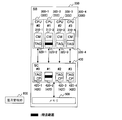
- FIG. 3 is a diagram illustrating a degeneracy range when a UE occurs in the TAG_CP memory 42-2 in the SC 4 as an example of the first embodiment.
- FIG. 4 is a diagram in the SC 4 as an example of the first embodiment.
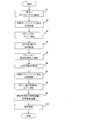
- 12 is a flowchart for explaining a degeneration process when a UE occurs in a TAG_CP memory 42-2.
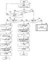
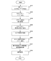
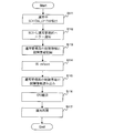
- the request control unit 44 When the TAG_CP error notification is input, the request control unit 44 notifies the command control unit 43 of a UE detection request suspension instruction (step S2). The command control unit 43 receives the hold instruction notification and holds the UE detection request in the hold state. Next, the request control unit 44 notifies the CPU 3-2 corresponding to the TAG_CP memory 42-2 in which the UE is detected, of the UE notification request including the index of the suspected place where the UE is detected and the WAY information ( Step S3).
- the CPU 3-2 Based on the received UE notification request, the CPU 3-2 saves all entries of the WAY of the CM 31-2 corresponding to the suspected place in the memory 5, and performs the WAY degeneration processing (step S4, in FIG. 3). (Refer to “Degenerate range” in the TAG memory 32-2). Specifically, the CPU 3 outputs a setting change request for invalidating the WAY corresponding to the suspected location to the register unit in the CPU 3, and the register unit sets a degeneration flag in the WAY corresponding to the suspected location in the configuration information. It is set and the WAY is invalidated. Thereafter, a degeneration process completion notification is transmitted from the CPU 3-2 to the request processing unit 44 (step S5).
- the request control unit 44 performs WAY degeneration processing corresponding to the suspected location in SC4 (see step S6, “degeneration range” of the TAG_CP memory 42-2 in FIG. 3). Specifically, the request processing unit 44 outputs a setting change request for invalidating the WAY corresponding to the suspected location to the register unit 46, and the register unit 46 degenerates to the WAY corresponding to the suspected location in the configuration information. A flag is set and the WAY is invalidated.
- the suspected part is guarded by the address lock register unit 45 so that the suspected part is not referred to by another request until the above-described degeneration processing of the CPU 3-2 and the TAG_CP memory 42-2 is completed. Thereby, multiple occurrence of UE can be prevented.
- the address lock register unit 45 deletes the address information related to the UE detection request held in the lock register 45a, and the request is unlocked.
- the request processing unit 44 After completion of the above-described degeneration processing of the CPU 3-2 and the TAG_CP memory 42-2, the request processing unit 44 notifies the command control unit 43 of an instruction to resume processing of the UE detection request that has been in a suspended state ( Step S7). In response to the notification of the process resumption instruction, the command control unit 43 resumes the process related to the UE detection request. Further, the request control unit 44 notifies the operation management unit 6 of error information related to the UE (step S8).
- the firmware of the operation management unit 6 records information about the degenerated WAY with respect to the control information managed by the operation management unit 6 as failure information (step S9). Then, the operation by the information processing system 1 is continued (step S10). Due to the above-described processing, the WAY degeneration processing corresponding to the suspected location is dynamically performed in the CPU 3 and SC4. Therefore, even when a UE occurs in the TAG_CP memory 42, operation stop can be avoided.
- the request notification unit 44 of the SC 4 notifies the CPU 3 of a UE notification request. Then, the CPU 3 performs WAY degeneration processing corresponding to the WAY generated by the UE based on the received UE notification request. Further, the request control unit 44 performs a degeneration process of the WAY generated by the UE in the TAG_CP memory 42.
- the information processing system 1 uses the TAG memory in the CPU 3 corresponding to the WAY in which the UE is detected, similarly to the case where the CE occurs in the TAG_CP memory 420 illustrated in FIG. 10 and FIG.
- the 32 WAYs and the WAY of the TAG_CP memory 42 in the SC 4 can be dynamically degenerated. Accordingly, the system can be continuously operated, and the availability of the information processing system 1 can be improved.
- the degeneration process accompanying the UE detection can be performed in units of WAYs, degeneration is performed in units of CPU 300 and TAG_CP memory 420 of SC 400 when a UE occurs as illustrated in FIGS. Compared with the conventional method to perform, the degeneracy range can be more limited. Further, in addition to the WAY degeneration processing corresponding to the suspected location in the TAG_CP memory 42, the WAY degeneration processing corresponding to the suspected location in the TAG memory 32 of the CPU 3 is also performed.
- the processing burden on the CPU 3 can be suppressed, and the performance of the information processing system 1 is greatly reduced when a UE occurs. Can be suppressed.
- the TAG_CP memories 42-1 to 42-4 correspond one-to-one with the TAG memories 32-1 to 32-4 in the CPUs 3-1 to 3-4. Therefore, even if a part (WAY) of the TAG_CP memory 42 is degenerated, the CPU 3 can access another CPU 3 other than the CPU 3 corresponding to the suspected place, so that the performance deterioration due to the retry of request issuance from the CPU 3 Can be prevented.
- the request control unit 44 of the SC 4 receives a UE processing request from the CPU 3 after receiving the degeneration processing completion notification of the TAG memory 32 from the CPU 3. An instruction to reissue is issued. As a result, since the UE detection request is reissued by the command control unit 43 after the degeneration processing is completed, the CPU 3 that has issued the UE detection request does not need to retry the UE detection request that has not been processed at the request destination.
- the processing load on the CPU 3 associated with the degeneration process related to the UE detection request it is possible to suppress a decrease in the performance of the information processing system 1 when a UE occurs. Furthermore, according to the information processing system 1 as an example of the first embodiment, until the WAY corresponding to the suspected place is degenerated in the CPU 3 and SC4 by the address lock register unit 45, the suspected place by another request is transferred to the suspected place. Access is suppressed.
- requests that have not been processed at the request source such as UE detection requests and subsequent requests to the suspected location, are reissued by the command control unit 43. Therefore, the suspected place can be guarded so that the cache tag data in which the UE is detected by another request is not referenced, and cache coherency can be maintained. That is, since the OS restart for degeneration of the CPU 3 itself corresponding to the TAG_CP memory 42 in which the UE occurred as illustrated in FIG. 13 is unnecessary, the system can be operated continuously, and the information processing system 1 The improvement of availability can be realized.
- Guarding the suspected UE occurrence location by the address lock register unit 45 is realized by using a guard function that guards a subsequent request so that it does not conflict with a request being processed. Furthermore, according to the information processing system 1 as an example of the first embodiment, when the address of the UE detection request is held in the lock register 45a by the address lock register unit 45, the same index and the full address are stored. When there is a mismatch, the area having the same index as the suspected part is also guarded. In this case, the address lock register unit 45 is configured so that the bit width of the address comparison can be made variable.
- the register unit 46 holds a degeneration flag indicating that the WAY of the TAG_CP memory 42 is degenerated.
- the request processing unit 44 can reliably set the degeneration flag even when a failure occurs in the address line system, for example, compared to the configuration including the degeneration flag in the TAG_CP memory 42.
- the degeneration process can be performed reliably.
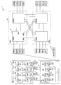
- FIG. 5 is a diagram illustrating a configuration of an information processing system 1 ′ as an example of the second embodiment.
- the information processing system 1 'in the second embodiment includes a plurality (16 in the example shown in FIG. 5) of SBs 2, an operation management unit 6, and a plurality (four in the example shown in FIG. 5). ) Crossbar (hereinafter referred to as XB) 9.
- the information processing system 1 ′ functions as an SMP server system using all or part of the plurality of SBs 2.
- the XB 9 is an LSI having a data transfer function between a plurality of SBs 2 and is mounted on a crossbar unit (indicated as XBU in FIG. 5) 8.
- the operation management unit 6 has the same configuration as that of the first embodiment, and is equipped with firmware for controlling the entire information processing system 1 ', that is, the CPU 3 and SC4 in each SB2. Further, the operation management unit 6 holds the information of the degenerated CPU 3 and the WAY information in each SB 2 as failure information in the control information managed by the operation management unit 6.
- the information processing system 1 ′ may include a storage unit (not shown) accessible from the SC 4 in each SB 2 as in the first embodiment.
- the SC 4 in the second embodiment can execute the process related to the request issued from the CPU 3 in the own SB 2 as in the first embodiment.
- the SC 4 in the second embodiment has a communication interface function between a plurality of SB 2, and when a request to the own SB 2 is issued via the XB 9 by the CPU 3 in the other SB 2, Such processing can be executed.
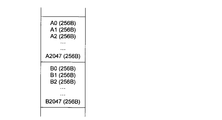
- FIG. 6 is a diagram illustrating an address map of the memory 5 as an example of the second embodiment
- FIG. 7 is a diagram illustrating a configuration of a TAG_CP memory 42 as an example of the second embodiment.
- one line in each WAY table corresponds to one cache tag data.
- the memory 5 in the second embodiment is managed by the SC 4 in units of cache lines (256 bytes) (blocks).
- the TAG_CP memory 42 in the SC 4 in the second embodiment manages the cache tag data in the form shown in FIG. That is, in the TAG_CP memory 42, 41:19 bits of the real address (PA) of the memory 5 are stored as the registered address of the cache tag data.
- the 7: 0 bit of the cache status (STS; Status) is stored in the cache tag data. Further, in the TAG_CP memory 42, the error correction code (ECC) of the cache tag data is added to the cache tag data as 7-bit data. An index that is a part of the real address of the memory 5 is used as the address of the TAG_CP memory 42 that stores the registration address and status described above.
- an index indicating a cache line is 11 bits and the number of cache lines is 2048 is illustrated. That is, in the example shown in FIG. 7, 18: 8 bits of the real address of the memory 5 are allocated to the index address. Therefore, in the address map of the memory 5 shown in FIG. 6, blocks having the same index (for example, A0 and B0) are assigned to the same index address as shown in FIG. These blocks having the same index are sequentially stored in WAY 0, WAY 1... WAY 11.
- the status in the cache tag data is represented by, for example, four states in the MOSI protocol.
- the MOSI protocol is a protocol that employs four cache statuses of M (Modified), O (Owned), S (Shared), and I (Invalid).
- M Modified
- O Owned
- S Shared
- I Invalid
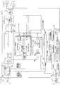
- FIG. 8 is a diagram illustrating a configuration of the SC 4 as an example of the second embodiment.
- SC4 illustrated in FIG. 8 further includes a pipe unit 47, a first I / F (Interface) unit 48, and a second I / F unit 49 in addition to the SC4 in the first embodiment.
- the SC4 illustrated in FIG. 8 includes the comparator 41a in the TAG_CP memory control unit 41, the address conflict checking unit 45b in the request control unit 44, and the register unit 46 in the register unit 46.
- a setting change unit 46a and a configuration control register 46b are provided.
- the command control unit 43 in the SC 4 illustrated in FIG. 8 includes a queue 43 a that holds the requests received from the CPU 3, and sequentially transfers the requests in the queue 43 a to the pipe unit 47 and via the pipe unit 47. Control for sequentially transferring to the TAG_CP memory control unit 41 and the address lock register unit 45 is performed. In addition, the command control unit 43 holds the request until the processing related to the transferred request is completed. When receiving a reissue (retry) instruction for the held request, the command control unit 43 registers the request relating to the reissue instruction again in the queue 43 a and reissues it.
- reissue retry
- the pipe unit 47 includes a plurality of latch circuits 47a-1 to 47a-n and 47b-1 to 47b-o (in FIG. 8, m, n and o are the number of latch circuits provided, M ⁇ n) and a result determination unit 47c.
- the pipe unit 47 inputs a request from the command control unit 43 to the latch circuit 47 a-1, and sends the request from the latch circuit 47 a-1 to the latch circuit 47 a-2, the TAG_CP memory control unit 41, and the address lock register unit 45. Respectively.
- the request input to the latch circuit 47a-2 sequentially passes through the latch circuits 47a-2 to 47a-n and is output to the result determination unit 47c in order to wait for search processing in the TAG_CP memory control unit 41.
- a request input to the TAG_CP memory control unit 41 and the address lock register unit 45 is subjected to a search process in the TAG_CP memory control unit 41, and is output to the latch circuit 47b-1 as a cache search result.
- the cache search result sequentially passes through the latch circuits 47b-1 to 47b-o and is output to the result determination unit 47c.
- the result determination unit 47c determines the transfer destination of the request based on the request that has passed through the latch circuits 47a-1 to 47a-n and the cache search result that has passed through the latch circuits 47b-1 to 47b-o.
- the data is output to the 1 I / F unit 48.
- the first I / F unit 48 sends the request output from the result determining unit 47c of the pipe unit 47 via the transfer destination determined by the result determining unit 47c, for example, the CPU 3 in the own SB2, the memory 5, or the XB9. It transmits to SC4 etc. in other SB2.
- the first I / F unit 48 transmits a request to the CPU 3 or the memory 5.
- the function is divided like the CPU I / F unit and the memory I / F unit. May be.
- each of the latch circuits 47a-1 to 47a-n and 47b-1 to 47b-o and a latch circuit 40a described later is, for example, a flip-flop.
- the latch circuits 47a-1 to 47a-n and 47b-1 to 47b-o adjust the timing at which the request and the cache search result are input to the result determination unit 47c.
- the TAG_CP memory control units 41-1 to 41-4 When a request from the command control unit 43 is input to the TAG_CP memory control units 41-1 to 41-4, as in the first embodiment, an index and a registered address are determined from the real address of the memory 5 included in the request. To extract. Then, the TAG_CP memory control units 41-1 to 41-4 search the cache tag data corresponding to the extracted index and registered address from the respective TAG_CP memories 42-1 to 42-4.
- the index is 18: 8 bits of the real address of the memory 5
- the registered address is 41:19 bits of the real address of the memory 5.
- the TAG_CP memory control unit 41 extracts the registered address of the same index from the TAG_CP memory 42 based on the index extracted from the request. Then, the TAG_CP memory control unit 41 compares the registered address extracted from the request (refer to the upper PA [41:19] in FIG. 8) with the registered address extracted from the TAG_CP memory 42, and matches. It is determined whether or not.
- the TAG_CP memory control unit 41 refers to the cache tag data including the matched registration address extracted from the TAG_CP memory 42.
- the cache tag data related to the request is hit or missed in the TAG_CP memory 42 by the search, the content of the subsequent processing is determined according to the content of the request and the status of the cache tag data. Since the determination of the contents of these processes can be realized by various known methods, detailed description thereof is omitted here.
- the request control unit 44 performs the same operation as in the first embodiment. In the example illustrated in FIG. 8, when a UE occurs in the TAG_CP memory 42, the request control unit 44 performs a WAY degeneration process of the TAG_CP memory 42 in which the UE has occurred. Notify the setting change request.
- the register setting change unit 46a sets a degeneration flag based on the setting change request for the configuration control register 46b that holds the configuration information.
- the request control unit 44 outputs an error information interrupt notification to the second I / F unit 49 having an interface function between the SC 4 and the operation management unit 6.
- the second I / F unit 49 outputs the interrupt notification to the operation management unit 6.
- the CE or UE when the CE or UE occurs, for example, when the number of WAYs operating in the TAG_CP memory 42 in which the CE or UE has occurred is less than or equal to a predetermined number (for example, 1), the SC 4 The generated TAG_CP memory 42 and the corresponding CPU 3 itself may be degenerated.
- the request control unit 44 degenerates the entire TAG_CP memory 42 in which the CE or UE has occurred when the number of WAYs operating in the TAG_CP memory 42 in which the CE or UE has occurred is equal to or less than a predetermined number.
- the CPU 3 itself corresponding to the TAG_CP memory 42 is degenerated.
- the degeneration process in this case can be performed by the method illustrated in FIG. 13 described above.
- the request control unit 44 operates in the TAG_CP memory 42 in which the CE or the UE has been generated by reading the setting information such as the degeneration flag set in the configuration control register 46b when the CE or the UE has occurred. The number of WAYs can be grasped. Further, the request control unit 44 may count the number of times CE has occurred, and notify the CPU 3 of a CE detection request when the number of times CE has occurred is greater than a predetermined threshold.
- the operation management unit 6 is based on failure information stored in the operation management unit 6.
- the WAY corresponding to the suspected place is degenerated again.
- the operation management unit 6 notifies the register setting change unit 46a of a setting change request based on the failure information via the second I / F unit 59.
- the register setting changing unit 46a sets a degeneration flag based on the setting change request to the configuration control register 46b that holds the configuration information.
- the CPU 3 in the second embodiment is also provided with a configuration control register (not shown), and the operation management unit 6 can also change the settings for the configuration control register provided in the CPU 3.
- the address lock register unit 45 When receiving a request from the command control unit 43, the address lock register unit 45 holds the address information in the request in the lock register 45a as in the first embodiment. Specifically, as shown in FIG. 8, the address lock register unit 45 obtains a full address (for example, 41: 3 bits in the second embodiment) from the real address in the request transferred from the command control unit 43. The index is extracted, and the extracted full address is held in the lock register 45a.
- a full address for example, 41: 3 bits in the second embodiment
- the address lock register unit 45 includes an address conflict checking unit 45b that compares the full address at the real address in the request being processed with the full address at the real address in the request held in the lock register 45a.
- the address conflict checking unit 45 b is provided in the request control unit 44, but is connected to the address lock register unit 45 and operates as a function of the address lock register unit 45. To do.
- the address conflict checking unit 45b may be provided in the address lock register unit 45.
- the address conflict checking unit 45b includes a comparator 45ba, and is input from the latch circuit 40a to PA [41: 3] of the comparator 45ba at the timing when the full address in the real address in the subsequent request is input to the latch circuit 40a. Is done.
- the full address in the real address in the request held in the lock register 45a is changed from the lock register 45a (REG_ADRS [41: 3] in the address lock register unit 45 in FIG. 8) to the REG_ADRS [41: in the comparator 45ba. 3].
- the comparator 45ba determines that the two input full addresses match in the address conflict checking unit 45b, the comparator 45ba indicates that the full address related to the subsequent request is busy. (Full address busy) is notified to the command control unit 43.
- the address lock register unit 45 in the second embodiment cancels and retries the process related to the subsequent request transferred from the command control unit 43, and conflicts with the request being processed, as in the first embodiment. It has a guard function to guard against
- the address lock register unit 45 in addition to the above-described processing, in the UE detection request until the degeneration processing of the suspected place by the CPU 3 and SC4 is completed when a UE occurs.
- the full address of the suspected place is held in the lock register 45a.
- the address conflict inspection unit 45b determines that the first address when the full address (PA [41: 3]) related to the subsequent request matches the full address (REG_ADRS [41: 3]) of the suspected location in the UE detection request.
- the command control unit 43 is notified of the full address busy of the subsequent request.
- the address lock register unit 45 receives the degeneration processing completion notification of the TAG memory 32 from the CPU 3, and until the request control unit 44 degenerates the WAY generated by the UE in the TAG_CP memory 42, The access to the TAG_CP memory 42 in which the occurrence has occurred is suppressed.
- the address lock register unit 45 in the second embodiment guards the processing related to the subsequent request so that it does not compete with the request being processed by the guard function, as in the first embodiment, and the UE is generated. If you do, you can guard the suspected place.
- a status update line is provided from each of the result determination unit 47 c of the pipe unit 47 and the first I / F unit 48 to each TAG_CP memory control unit 41 and the address lock register unit 45. Is provided.
- the status update in each TAG_CP memory control unit 41 and the lock control in the address lock register unit 45 are performed.
- the address lock register unit 45 receives information indicating the maintenance of the lock from the result confirmation unit 47c via the status update line, and locks the UE detection request in the lock register 45a. Can be maintained.
- the address lock register unit 45 receives information indicating the maintenance of the lock from the result confirmation unit 47c via the status update line, and locks the UE detection request in the lock register 45a. Can be maintained.
- FIG. 9 is a flowchart for explaining a degeneration process when a CE or UE occurs in the TAG_CP memory 42-2 in the SC 4 as an example of the second embodiment.
- the detected error is detected by the SC4. It is determined whether or not it is CE (step S12).
- the request control unit 44 determines whether the number of CE occurrences is greater than a predetermined threshold (step S13). When it is determined that the CE occurrence number is equal to or less than the predetermined threshold (No route in step S13), the request control unit 44 increments the value of the counter that counts the CE occurrence number, and operates the information processing system 1 ′. Return.
- the request control unit 44 determines that the number of WAYs operating in the TAG_CP memory 42-2 in which the CE has occurred is a predetermined number. It is determined whether (1 here) or less (step S14). When it is determined that the number of operating WAYs is larger than 1 (No route in step S14), the CE is notified from the request control unit 44 to the CPU 3-2 corresponding to the TAG_CP memory 42-2 in which the CE has occurred. The request is notified (step S15). This request includes the index of the suspected place corrected by the ECC and the WAY information.
- the CPU 3-2 sweeps the cache data of the WAY in the TAG memory 32-2 in which the CE has occurred to the memory, and the Degeneration processing is performed (step S16). Then, the CPU 3-2 notifies the SC4 of the completion of the degeneration process (step S17).
- the request control unit 44 performs the degeneration process on the WAY of the TAG_CP memory 42-2 in which the CE has occurred (step S18). Then, the request control unit 44 notifies the operation management unit 6 of error information about CE (step S19), and the failure information is recorded in the control information of the operation management unit 6 (step S20). Thereafter, the operation is continued in the information processing system 1 ′ (step S21).
- Step S14 when the request control unit 44 determines that the number of operating WAYs is 1 or less in Step S14 (Yes route in Step S14), CE is generated from the request control unit 44 to the operation management unit 6. Then, the CPU 3-2 performs a degeneration process and is notified by an interrupt (step S22). After the interrupt notification, the operation management unit 6 records information indicating the CPU 3-2 having the TAG memory 32 corresponding to the TAG_CP memory 42-2 to be suspected and WAY information as failure information in the control information managed by itself. (Step S23). Then, the OS being executed in the information processing system 1 ′ is restarted by the operation management unit 6 (step S24).
- the failure information of the control information is read by the operation management unit 6 (step S25), and the CPU 3-2 recorded in the failure information is not started up, and other normal CPUs 3-
- the start-up process is performed only for 1, 3-3 and 3-4. That is, the operation management unit 6 degenerates the CPU 3-2 corresponding to the suspected place (step S26). Thereafter, the operation is resumed in the information processing system 1 ′ (step S27).
- step S12 when it is determined in step S12 that the detected error is not a CE, that is, a UE (No route in step S12), the request control unit 44 operates in the TAG_CP memory 42-2 in which the UE has occurred. It is determined whether or not the number of WAYs is less than or equal to a predetermined number (here, 1) (step S28). If it is determined that the number of operating WAYs is greater than 1 (No route in step S28), the processes in steps S2 to S10 described above with reference to FIG. 4 are performed (step S29).
- a predetermined number here, 1
- the TAG_CP memory control unit 41 notifies the request control unit 44 of a TAG_CP error notification, and the request control unit 44 notifies the command control unit 43 of a hold instruction for the UE detection request (step S2). Then, the UE detection request is held in the command control unit 43 as a pending state. Next, the request control unit 44 notifies the CPU 3-2 corresponding to the TAG_CP memory 42-2 in which the UE has been detected (step S3).
- step S4 the WAY degeneration process of the CM 31-2 corresponding to the suspected place is performed (step S4), and a degeneration process completion notification is transmitted to the request processing unit 44 (step S5). Further, the request control unit 44 performs WAY degeneration processing corresponding to the suspected place in the SC 4 (step S6).
- the request processing unit 44 After the degeneration processing completion notification is notified from the CPU 3-2 and the WAY degeneration processing of the TAG_CP memory 42-2 in which the UE is detected is completed, the request processing unit 44 causes the command control unit 43 to resume processing of the UE detection request. Is notified (step S7). In the command control unit 43, processing related to the UE detection request is resumed (reissued). Then, the request control unit 44 notifies the operation management unit 6 of the error information related to the UE (Step S8).
- the firmware of the operation management unit 6 stores the information about the degenerated WAY with respect to the control information managed by the operation management unit 6 as failure information (step S9), and the information processing system 1 The operation by ′ is continued (step S10).
- the request control unit 44 determines that the number of operating WAYs is 1 or less in Step S28 (Yes route in Step S28)
- a UE is generated from the request control unit 44 to the operation management unit 6.
- the CPU 3-2 is notified of the interruption process (step S22). Thereafter, the processing after step S23 described above is performed for the CPU 3-2 corresponding to the TAG_CP memory 42 in which the UE has occurred.
- the request control unit 44 counts the number of CE occurrences, and when the number of CE occurrences is larger than a predetermined threshold, the CE detection request Is notified to the CPU 3.
- the number of CPUs 3 in the SB 2 is four has been described.
- the number of CPUs 3 is not limited to this, and may be one or another number. But it ’s okay.
- a TAG_CP memory 42 corresponding to each TAG memory 32 (CPU 3) may be provided in SC 4.
- the request for which the UE has been detected is suspended until the target WAY degeneration process in the CPU 3 and SC 4 is completed.
- the present invention is not limited to this. is not.
- the SC 4 can confirm from the cache tag data that there is the latest data in another CPU 3, that is, a CPU 3 different from the CPU 3 corresponding to the TAG_CP memory 42 in which the UE is detected.
- the UE detection request may be processed as usual. If there is the latest data in another CPU, the status of the cache tag data in the TAG_CP memory 42 of the other WAY for the request in which the UE is detected is, for example, “M” or “O” in the MOSI protocol. .
- the process of releasing the address lock in the normal process that is, the UE detection request is processed as usual, and the process of deleting the address from the lock register 45a after the completion of the process is suppressed. Then, after the CM 31 data sweep-out process associated with the degeneration process of the CPU 3 is completed, a process for releasing the address lock is performed. For this reason, it is preferable that information indicating that the status relating to the request is “M” or “O” is added to the address held in the lock register 45 a or the data passing through the pipe unit 47.
- the UE may be allowed to occur a plurality of times until the CM 31 data sweep-out process associated with the degeneration process of the CPU 3 is completed.
- the UE detection request is suspended. Processing delay can be prevented.
- Step S22 to Step S27 from the Yes route of Step S14 that is, CE occurs in the TAG_CP memory 42, and the TAG_CP memory 42 in which CE has occurred.
- the processing in the case where the number of WAYs operating in is not more than a predetermined number is not limited to this.
- the information processing system 1 ′ may continue the operation as it is without executing the processing of steps S22 to S27.
- Step S22 to Step S27 from the Yes route of Step S28 that is, the UE is generated in the TAG_CP memory 42, and the TAG_CP memory 42 in which the UE is generated
- the processing in the case where the number of WAYs operating in is not more than a predetermined number is not limited to this.
- the information processing system 1 ′ does not execute the processing of steps S22 to S27, but the SC 4 notifies the OS that a UE has occurred in the last WAY, and the OS terminates all processes being processed. Then, the shutdown (Shutdown) process may be performed.
- the process in step S6 may be performed before the process in steps S3 to S5 or between steps S3 and S5.
- the WAY degeneration processing of the TAG_CP memory 42 in which the UE has occurred by the request processing unit 44 may be performed before the WAY degeneration processing of the CPU 3 corresponding to the WAY or may be performed in parallel. good.
Landscapes
- Engineering & Computer Science (AREA)
- Theoretical Computer Science (AREA)
- Physics & Mathematics (AREA)
- General Engineering & Computer Science (AREA)
- General Physics & Mathematics (AREA)
- Quality & Reliability (AREA)
- Memory System Of A Hierarchy Structure (AREA)
- Techniques For Improving Reliability Of Storages (AREA)
Abstract
システムコントローラ(4)は、演算処理装置(3)の第1タグメモリ(32)に対応する第2タグメモリ(42)から読み出されたデータが訂正不可能なエラーであるUE(Uncorrectable Error)を起こした場合に、前記UEが発生した前記第2タグメモリ(42)のウェイ情報を前記演算処理装置(3)に通知し、前記演算処理装置(3)は、通知されたウェイ情報に基づいて対応する前記第1タグメモリ(32)のウェイを縮退させ、縮退処理の完了を前記システムコントローラ(4)へ通知して、前記システムコントローラ(4)は、前記第2タグメモリ(42)のUEが発生したウェイを縮退させるとともに、前記演算処理装置(3)から前記第1タグメモリ(32)の縮退処理が完了した旨の通知を受信した後、当該UEに係るリクエストを再発行する。
Description
本件は、情報処理装置,及びキャッシュ制御方法に関する。
近年、処理の高速化や耐障害性の向上を図るため、対称型マルチプロセッシング(SMP;Symmetric Multi Processor)方式を用いた、SMPサーバシステムが用いられることがある。
SMPは、複数のCPU(Central Processing Unit)が同等な立場で処理を分担するマルチプロセッサ手法であり、CPUキャッシュを同期させる機能や処理に用いられる各種資源を管理する機能を備える。
SMPは、複数のCPU(Central Processing Unit)が同等な立場で処理を分担するマルチプロセッサ手法であり、CPUキャッシュを同期させる機能や処理に用いられる各種資源を管理する機能を備える。
SMPサーバシステムは、複数のCPUやシステムコントローラ(System Controller;以下、SCという)や、RAM(Random Access Memory)等のメモリのほか、システムを制御するファームウェアが搭載された運用管理部などにより構成される。
このようなSMPサーバシステムでは、処理速度の向上のために、CPUのキャッシュタグ(TAG)データのコピー(TAG_CP)をSC内に備えることがある。この場合、各CPUからの問い合わせに対し、対象CPUの前段にあるSCにより、TAG_CPが参照されて応答が返される。これにより、スヌープ方式による高速なキャッシュアクセスを実現し、CPUのキャッシュメモリ(Cache Memory;以下、CMという)の同期処理の高速化を実現する。
このようなSMPサーバシステムでは、処理速度の向上のために、CPUのキャッシュタグ(TAG)データのコピー(TAG_CP)をSC内に備えることがある。この場合、各CPUからの問い合わせに対し、対象CPUの前段にあるSCにより、TAG_CPが参照されて応答が返される。これにより、スヌープ方式による高速なキャッシュアクセスを実現し、CPUのキャッシュメモリ(Cache Memory;以下、CMという)の同期処理の高速化を実現する。
なお、スヌープ方式とは、キャッシュコヒーレンシのアルゴリズムの一つであり、他のキャッシュと更新状態の情報を交換することで、どのキャッシュに最新のデータが格納されているかを把握することができ、最新のデータを取得することができるものである。
また、近年、CPUのCMにおいて、キャッシュライン数の増加に伴い、複数のWAYによるデータ格納構造であるセットアソシアティブ構成が採用されている。
また、近年、CPUのCMにおいて、キャッシュライン数の増加に伴い、複数のWAYによるデータ格納構造であるセットアソシアティブ構成が採用されている。
セットアソシアティブ構成では、CPUのCMにおいて、キャッシュライン毎に複数のWAYが備えられ、各WAYにデータが格納される。
キャッシュタグデータは、CPU内部のTAGメモリ及びSC内部のTAG_CPメモリにそれぞれ格納され、インデックスと呼ばれるメモリの物理アドレスの一部を使用したアドレスにより管理される。キャッシュタグデータは、CPUからのリクエストに応じて、インデックスにより特定されるCM内の一のキャッシュラインから、一のWAYを絞り込み、CMから所望のデータを取得するのに用いられる。
キャッシュタグデータは、CPU内部のTAGメモリ及びSC内部のTAG_CPメモリにそれぞれ格納され、インデックスと呼ばれるメモリの物理アドレスの一部を使用したアドレスにより管理される。キャッシュタグデータは、CPUからのリクエストに応じて、インデックスにより特定されるCM内の一のキャッシュラインから、一のWAYを絞り込み、CMから所望のデータを取得するのに用いられる。
なお、CM、TAGメモリ及びTAG_CPメモリとしては、いずれもSRAM(Static RAM)等のRAMが挙げられる。
上述したSMPサーバシステムでは、CPU、CM、TAGメモリ又はTAG_CPメモリ等の障害が検出されると、運用管理部によって、異常が発生した箇所をシステムから切り離す縮退処理が行なわれる。この縮退処理により、システムの動作を中断することなく運用を継続することができ、耐障害性の向上が実現される。
上述したSMPサーバシステムでは、CPU、CM、TAGメモリ又はTAG_CPメモリ等の障害が検出されると、運用管理部によって、異常が発生した箇所をシステムから切り離す縮退処理が行なわれる。この縮退処理により、システムの動作を中断することなく運用を継続することができ、耐障害性の向上が実現される。
特にミッションクリティカルな分野で使用される大規模SMPサーバシステムで、TAG_CPメモリ等の故障が発生した場合、システムの性能が低下することになるとしても、被疑箇所を切り離して運用を継続することが望ましい。このため、従来のSMPサーバシステムには、CPU内部のTAGメモリやSC内部のTAG_CPメモリの固定的な1ビット(bit)故障が発生した場合、被疑箇所のWAYを動的に縮退し、運用を停止させずに故障箇所を切り離す仕組みが実装されている。
なお、1ビット故障では、キャッシュタグデータに含まれるエラー訂正符号(Error Correcting Code;以下、ECCという)により、エラーの訂正が可能である。以下、1ビット故障を訂正可能エラー又はCE(Correctable Error)という。
以下、SC内のTAG_CPメモリでCEが発生した場合の、システムの縮退処理の動作を説明する。
以下、SC内のTAG_CPメモリでCEが発生した場合の、システムの縮退処理の動作を説明する。
図10は、SC400内のTAG_CPメモリ420-2でCEが発生した場合の縮退範囲を示す図であり、図11は、SC400内のTAG_CPメモリ420-2でCEが発生した場合の縮退処理を説明するためのフローチャートである。
図10に例示するように、SMPサーバシステムでは、システムボード(SB;System Board:以下、SBという)200と、運用管理部600とが備えられる。
図10に例示するように、SMPサーバシステムでは、システムボード(SB;System Board:以下、SBという)200と、運用管理部600とが備えられる。
また、SB200には、CPU300-1~300-4と、SC400と、メモリ500とが備えられる。なお、以下の説明においてCPU300-1~300-4を区別しない場合には、単にCPU300という。
各CPU300-1~300-4には、それぞれCM310-1~310-4及びTAGメモリ320-1~320-4が備えられる。なお、CM310-1~310-4及びTAGメモリ320-1~320-4の符号におけるハイフン“-”の右側の数字は、CM310-1~310-4及びTAGメモリ320-1~320-4が、それぞれ対応する数字のCPU300-1~300-4に備えられることを示す。
各CPU300-1~300-4には、それぞれCM310-1~310-4及びTAGメモリ320-1~320-4が備えられる。なお、CM310-1~310-4及びTAGメモリ320-1~320-4の符号におけるハイフン“-”の右側の数字は、CM310-1~310-4及びTAGメモリ320-1~320-4が、それぞれ対応する数字のCPU300-1~300-4に備えられることを示す。
さらに、SC400には、TAGメモリ320-1~320-4に対応したTAG_CPメモリ420-1~420-4が備えられる。なお、以下の説明においてTAG_CPメモリ420-1~420-4を区別しない場合には、単にTAG_CPメモリ420という。
図10及び図11に示すように、システムの運用中、SC400内のTAG_CPメモリ420-2にCEが発生し、SC400により検出された場合(ステップS101)、SC400からCEが発生したTAG_CPメモリ420に対応するCPU300-2に対して、被疑箇所の情報が通知される(ステップS102)。なお、この情報には、ECCにより訂正された被疑箇所のインデックスと、WAY番号とが含まれる。
図10及び図11に示すように、システムの運用中、SC400内のTAG_CPメモリ420-2にCEが発生し、SC400により検出された場合(ステップS101)、SC400からCEが発生したTAG_CPメモリ420に対応するCPU300-2に対して、被疑箇所の情報が通知される(ステップS102)。なお、この情報には、ECCにより訂正された被疑箇所のインデックスと、WAY番号とが含まれる。
CPU300-2では、通知された被疑箇所に対応したTAGメモリ320-2内のWAYのデータがメモリに掃き出されるとともに、当該WAYの縮退処理が行なわれる(ステップS103)。そして、CPU300-2により、SC400へ縮退処理完了の通知が行なわれる(ステップS104)。
縮退処理完了通知を受けたSC400では、被疑箇所のWAYに対して縮退処理が行なわれる(ステップS105)。そして、SC400により、運用管理部600に対して、縮退処理を行なったCPU300-2のWAY番号を含むエラー通知が行なわれ(ステップS106)、運用管理部600の制御情報に故障情報が記録される(ステップS107)。その後、SMPサーバシステムでは運用が継続される(ステップS108)。
縮退処理完了通知を受けたSC400では、被疑箇所のWAYに対して縮退処理が行なわれる(ステップS105)。そして、SC400により、運用管理部600に対して、縮退処理を行なったCPU300-2のWAY番号を含むエラー通知が行なわれ(ステップS106)、運用管理部600の制御情報に故障情報が記録される(ステップS107)。その後、SMPサーバシステムでは運用が継続される(ステップS108)。
上述の如く、CPU300-2内部のTAGメモリ320-2の一部(WAY)及びSC400内部のTAG_CPメモリ420-2の一部(WAY)が縮退される(図10中、「縮退範囲」参照)。これにより、システムに多少の性能低下は発生するものの、縮退処理は動的に行なわれるため、運用の停止を回避することができる。
なお、ステップS107において運用管理部600の制御情報に記録された故障情報は、例えばSMPサーバシステムで実行中のOS(Operating System)の再起動等によってCPU及びSC内の縮退状態がリセットされた場合に、被疑箇所のWAYを再度縮退させるために用いられる。
なお、ステップS107において運用管理部600の制御情報に記録された故障情報は、例えばSMPサーバシステムで実行中のOS(Operating System)の再起動等によってCPU及びSC内の縮退状態がリセットされた場合に、被疑箇所のWAYを再度縮退させるために用いられる。
ところで、SC内部のTAG_CPメモリにエラーの訂正が不可能な故障が発生した場合、SCは、ECCによりエラーの訂正を行なうことができず、キャッシュコヒーレンシを保つことができない。このため、従来のSMPサーバシステムには、SC内のTAG_CPメモリでエラーの訂正が不可能な故障が発生した場合、被疑箇所に対応するCPUを縮退し、運用を一度停止させて故障箇所を切り離す仕組みが実装されている。
なお、エラーの訂正が不可能な故障とは、キャッシュタグに含まれるECCによってもエラーを訂正することが不可能な故障であり、例えば、2ビット以上の領域の故障である。以下、2ビット以上の領域の故障(多ビット故障)を、訂正不可能エラー又はUE(Uncorrectable Error)という。
以下、SC内のTAG_CPメモリでCEが発生した場合の、システムの縮退処理の動作を説明する。
以下、SC内のTAG_CPメモリでCEが発生した場合の、システムの縮退処理の動作を説明する。
図12は、図10に示すものと同様の構成のSB200及び運用管理部600において、SC400内のTAG_CPメモリ420-2でUEが発生した場合の縮退範囲を示す図である。また、図13は、SC400内のTAG_CPメモリ420-2でUEが発生した場合の縮退処理を説明するためのフローチャートである。
図12及び図13に示すように、システムの運用中、SC400内のTAG_CPメモリ420-2にUEが発生し、SC400により検出された場合(ステップS111)、SC400から運用管理部600に対して、UEが発生したことが割り込みで通知される(ステップS112)。
図12及び図13に示すように、システムの運用中、SC400内のTAG_CPメモリ420-2にUEが発生し、SC400により検出された場合(ステップS111)、SC400から運用管理部600に対して、UEが発生したことが割り込みで通知される(ステップS112)。
運用管理部600では、割り込み通知に基づいて、被疑箇所に対応したCPU300-2を示す情報とWAY番号とが故障情報として、運用管理部600の制御情報に記録される(ステップS113)。そして、運用管理部600により、SMPサーバシステムで実行中のOSが再起動される(ステップS114)。
OSの再起動後、運用管理部600により、制御情報の故障情報が読み込まれ(ステップS115)、故障情報に記録されているCPU300-2は、立ち上げ処理が行なわれず、他の正常なCPU300-1、300-3及び300-4についてのみ立ち上げ処理が行なわれる。つまり、運用管理部600により、被疑箇所に対応するCPU300-2及び被疑箇所に対応するTAG_CPメモリ420-2が縮退処理された状態で、OSが立ち上がる(ステップS116,図12中、「縮退範囲」参照)。その後、SMPサーバシステムでは、運用が再開される(ステップS117)。
OSの再起動後、運用管理部600により、制御情報の故障情報が読み込まれ(ステップS115)、故障情報に記録されているCPU300-2は、立ち上げ処理が行なわれず、他の正常なCPU300-1、300-3及び300-4についてのみ立ち上げ処理が行なわれる。つまり、運用管理部600により、被疑箇所に対応するCPU300-2及び被疑箇所に対応するTAG_CPメモリ420-2が縮退処理された状態で、OSが立ち上がる(ステップS116,図12中、「縮退範囲」参照)。その後、SMPサーバシステムでは、運用が再開される(ステップS117)。
このように、SC400内部のTAG_CPメモリ420でUEが発生した場合には、SMPサーバシステムの運用が停止し、被疑箇所を含む全コンポーネント(例えば1つのCPU300全体)を縮退後、運用を再開するという手法が採られる。
なお、他に、キャッシュメモリを搭載した複数のCPUを備えたマルチプロセッサシステムにおいて、メモリコントロール/コヒーレンシ制御装置が備えるタグメモリから索引されたタグ索引結果に訂正不可能障害が発生した場合であっても、動作を継続できるようにする技術が知られている。
なお、他に、キャッシュメモリを搭載した複数のCPUを備えたマルチプロセッサシステムにおいて、メモリコントロール/コヒーレンシ制御装置が備えるタグメモリから索引されたタグ索引結果に訂正不可能障害が発生した場合であっても、動作を継続できるようにする技術が知られている。
具体的には、メモリコントロール/コヒーレンシ制御装置が、タグメモリから索引されたタグ索引結果に訂正不可能障害を検出した場合、各CPUに対して、訂正不可能障害が検出されたタグ索引結果に関連する可能性がある全てのデータを主記憶装置に掃き出すように指示する。これにより、データのコヒーレンシを保障することができる。
なお、訂正不可能障害が検出されたタグ索引結果に関連する可能性がある全てのデータとは、キャッシュメモリに格納されているデータの内の、下位アドレスがタグ索引時に用いられた下位アドレスと一致する全てのデータをいう。
なお、訂正不可能障害が検出されたタグ索引結果に関連する可能性がある全てのデータとは、キャッシュメモリに格納されているデータの内の、下位アドレスがタグ索引時に用いられた下位アドレスと一致する全てのデータをいう。
従来、TAG_CPメモリにおける訂正不可能エラー(UE)の発生頻度が低かったため、図12及び図13に例示したように、UEが発生した場合には、被疑箇所に対応したCPU及び被疑箇所のSC内のTAG_CPメモリを縮退処理させる運用が行なわれていた。
しかしながら、UEが発生した場合の上述した手法では、運用が停止する時間が発生し、SMPサーバシステムの可用性が低下するという問題がある。
しかしながら、UEが発生した場合の上述した手法では、運用が停止する時間が発生し、SMPサーバシステムの可用性が低下するという問題がある。
また、近年、LSI(Large Scale Integration)内部の集積度が増すことによりCM容量が増加している。また、SMPサーバシステムに搭載されるCPU数の増加に伴い、SMPサーバシステム内の総CM容量が増加している。このようなSMPサーバシステム内のCM容量の増加によって、以前に比べてUEが発生する確率が高くなっている。
このように、UEの発生確率が高くなっている現状において、SMPサーバシステムの可用性が低下する場面(頻度)が増加するという問題もある。
このように、UEの発生確率が高くなっている現状において、SMPサーバシステムの可用性が低下する場面(頻度)が増加するという問題もある。
さらに、上述したメモリコントロール/コヒーレンシ制御装置を用いた技術では、訂正不可能エラーが検出された場合でもデータのコヒーレンシを保障することができるが、以下の(i)及び(ii)に示す問題がある。
(i)メモリコントロール/コヒーレンシ制御装置内のタグ部で訂正不可能エラーが発生してタグ部の一部が縮退された場合、CPUは、タグ部の一部が縮退されたことを知らないため、CPUから、縮退されたタグ部の一部を再使用するようなリクエストが送信される可能性がある。このようなリクエストが送信された場合、メモリコントロール/コヒーレンシ制御装置は、リクエストに従ったタグ部の使用が不可能であるという応答、或いはキャッシュをタグ部に登録せずに使用するという応答をCPUに返すことになる。
(i)メモリコントロール/コヒーレンシ制御装置内のタグ部で訂正不可能エラーが発生してタグ部の一部が縮退された場合、CPUは、タグ部の一部が縮退されたことを知らないため、CPUから、縮退されたタグ部の一部を再使用するようなリクエストが送信される可能性がある。このようなリクエストが送信された場合、メモリコントロール/コヒーレンシ制御装置は、リクエストに従ったタグ部の使用が不可能であるという応答、或いはキャッシュをタグ部に登録せずに使用するという応答をCPUに返すことになる。
このような場合、以下の(i-1)~(i-3)に示す状況において、それぞれシステムの性能低下が発生するという問題がある。
(i-1)CPUは、上述の応答を受けることを許容していない場合、つまり上述の応答に対する処理が定義されておらず対応できない場合には、動作不能に陥る可能性がある。
(i-1)CPUは、上述の応答を受けることを許容していない場合、つまり上述の応答に対する処理が定義されておらず対応できない場合には、動作不能に陥る可能性がある。
(i-2)また、CPUは、上述の応答を許容し動作を行なう場合でも、CPUによる処理によっては、縮退されたタグ部の一部を再使用するようなリクエストがメモリコントロール/コヒーレンシ制御装置に繰り返し出力されるおそれがある。このような状況では、CPU及びメモリコントロール/コヒーレンシ制御装置間で、上述したリクエスト及び応答が繰り返し行なわれるため、システムの性能低下を招くことになる。
(i-3)或いは、メモリコントロール/コヒーレンシ制御装置は、タグ索引時に用いられた下位アドレスと同じ下位アドレスの別WAYのデータの掃き出し指示を、リクエストに対する応答を返す前に、リクエスト要求元のCPUに対して行なうことが考えられる。この場合、メモリコントロール/コヒーレンシ制御装置は、CPUによる掃き出し完了後、元のリクエストに対する応答を要求元のCPUに返すような動作を行なう。これにより、データのコヒーレンシを保つことはできるが、上述の如く、CPUにより上述の応答に対する処理が行なわれ、システムの性能低下を招くことになる。
(ii)また、メモリコントロール/コヒーレンシ制御装置は、エントリの縮退状態を示すエントリ使用不可フラグをタグメモリに備える。しかし、タグメモリのアドレスライン系で故障が発生した場合には、エントリ使用不可フラグ自体を正しく読み出せない可能性がある。
すなわち、タグメモリのアドレスライン系で故障が発生した場合、タグメモリのセルに対するアクセスが正常に行なわれず、エントリ使用不可フラグ自体を正しく読み出せないことがある。従って、実際にはエントリ使用不可フラグに縮退を示す情報が設定されている場合であっても、システムからは縮退したように見えず、リトライが行なわれる度にUEの発生が検出されて、処理不能に陥る可能性がある。
すなわち、タグメモリのアドレスライン系で故障が発生した場合、タグメモリのセルに対するアクセスが正常に行なわれず、エントリ使用不可フラグ自体を正しく読み出せないことがある。従って、実際にはエントリ使用不可フラグに縮退を示す情報が設定されている場合であっても、システムからは縮退したように見えず、リトライが行なわれる度にUEの発生が検出されて、処理不能に陥る可能性がある。
なお、エントリ使用不可フラグを、タグメモリではなく、例えばエントリ毎にラッチで備えることも考えられるが、物量的に困難である。
上述の点に鑑み、本件の目的の1つは、情報処理装置の可用性の向上を実現することである。
なお、前記目的に限らず、後述する発明を実施するための形態に示す各構成により導かれる作用効果であって、従来の技術によっては得られない作用効果を奏することも本発明の他の目的の1つとして位置付けることができる。
上述の点に鑑み、本件の目的の1つは、情報処理装置の可用性の向上を実現することである。
なお、前記目的に限らず、後述する発明を実施するための形態に示す各構成により導かれる作用効果であって、従来の技術によっては得られない作用効果を奏することも本発明の他の目的の1つとして位置付けることができる。
本件の情報処理装置は、キャッシュメモリ及び第1タグメモリを有する演算処理装置と、前記演算処理装置と他の処理装置との通信制御を行なうシステムコントローラとを有する情報処理装置であって、前記システムコントローラは、前記演算処理装置から受信したリクエストを保持し、当該リクエストが要求先において処理されなかった場合に当該リクエストを再発行するコマンド制御部と、前記第1タグメモリに記憶されるデータの複製データを保持する第2タグメモリと、前記第2タグメモリから読み出されたデータが訂正不可能なエラーであるUEを起こした場合に、前記UEが発生した第2タグメモリのウェイ情報を前記演算処理装置に通知するリクエスト制御部とを有し、前記演算処理装置は、前記リクエスト制御部から前記UEが発生した通知を受けると、当該UEが発生した前記第2タグメモリのウェイに対応する前記第1タグメモリのウェイを縮退させて、前記第1タグメモリのウェイの縮退処理が完了したことを前記リクエスト制御部へ通知し、前記リクエスト制御部は、前記UEが発生した場合に、前記第2タグメモリのUEが発生したウェイを縮退させるとともに、前記演算処理装置から、前記第1タグメモリの縮退処理が完了した旨の通知を受信した後、前記コマンド制御部に当該UEに係るリクエストを再発行させる指示を行なうものである。
また、本件のキャッシュ制御方法は、キャッシュメモリ及び第1タグメモリを有する演算処理装置と、前記演算処理装置と他の処理装置との通信制御を行なうシステムコントローラとを有する情報処理装置のキャッシュ制御方法であって、前記システムコントローラにおいて、前記第1タグメモリに記憶されるデータの複製データを保持する第2タグメモリから読み出されたデータが訂正不可能なエラーであるUEを起こした場合に、前記UEが発生した前記第2タグメモリのウェイ情報を前記演算処理装置に通知し、前記演算処理装置において、前記UEが発生した通知を受けると、当該UEが発生した前記第2タグメモリのウェイに対応する前記第1タグメモリのウェイを縮退させて、前記第1タグメモリのウェイの縮退処理が完了したことを前記システムコントローラへ通知して、前記システムコントローラにおいて、前記演算処理装置から、前記第2タグメモリのUEが発生したウェイを縮退するとともに、前記第1タグメモリの縮退処理が完了した旨の通知を受信した後、当該UEに係るリクエストを再発行するものである。
開示の技術によれば、情報処理装置の可用性の向上を実現することができる。
以下、図面を参照して本発明の実施の形態を説明する。
〔1〕第1実施形態
〔1-1〕第1実施形態の構成
図1は、第1実施形態の一例としての情報処理システム1の構成を示す図である。
図1に示すように、情報処理システム(情報処理装置)1は、SB2と、運用管理部6とを備える。
〔1〕第1実施形態
〔1-1〕第1実施形態の構成
図1は、第1実施形態の一例としての情報処理システム1の構成を示す図である。
図1に示すように、情報処理システム(情報処理装置)1は、SB2と、運用管理部6とを備える。
情報処理システム1は、例えば、SMPサーバシステムである。
また、第1実施形態における情報処理システム1は、SC4内のTAG_CPメモリ42においてCEが発生した場合に、図11に示す上述した手法により、運用を継続することができる。なお、第1実施形態においては、CEが発生した場合の情報処理システム1の動作については、その詳細な説明を省略する。
また、第1実施形態における情報処理システム1は、SC4内のTAG_CPメモリ42においてCEが発生した場合に、図11に示す上述した手法により、運用を継続することができる。なお、第1実施形態においては、CEが発生した場合の情報処理システム1の動作については、その詳細な説明を省略する。
第1実施形態における情報処理システム1は、SC4内のTAG_CPメモリ42においてUEが発生した場合に、後述の如く、UEが発生したTAG_CPメモリ42のWAY及び当該WAYに対応するCPU3のTAGメモリ32のWAYを動的に縮退させることで、運用を継続させることができる。
SB2は、少なくとも1つ(第1実施形態においては4つ)のCPU3-1~3-4と、SC4と、RAM等のメモリ5とを備える。なお、以下の説明においてCPU3-1~3-4を区別しない場合には、単にCPU3という。
SB2は、少なくとも1つ(第1実施形態においては4つ)のCPU3-1~3-4と、SC4と、RAM等のメモリ5とを備える。なお、以下の説明においてCPU3-1~3-4を区別しない場合には、単にCPU3という。
CPU3-1~3-4は、それぞれSC4に接続され、情報処理システム1における種々の制御や演算を行なう演算処理装置であり、例えば、記憶部(図示省略)に格納されたプログラムをメモリ5に展開して実行することにより、種々の機能を実現する。
CPU3-1~3-4は、それぞれCM31-1~31-4及びTAGメモリ(第1タグメモリ)32-1~32-4を備える。以下の説明においてCM31-1~31-4を区別しない場合には、単にCM31という。また、TAGメモリ32-1~32-4を区別しない場合には、単にTAGメモリ32という。
CPU3-1~3-4は、それぞれCM31-1~31-4及びTAGメモリ(第1タグメモリ)32-1~32-4を備える。以下の説明においてCM31-1~31-4を区別しない場合には、単にCM31という。また、TAGメモリ32-1~32-4を区別しない場合には、単にTAGメモリ32という。
なお、CM31-1~31-4及びTAGメモリ32-1~32-4の符号におけるハイフン“-”の右側の数字は、CM31及びTAGメモリ32が、それぞれ対応する数字のCPU3-1~3-4に備えられることを示す。
CM31は、CPU3とメモリ5との間で転送されるデータを格納する。なお、第1実施形態においては、CM31が、nWAYセットアソシアティブ方式を採用する場合について例示する。
CM31は、CPU3とメモリ5との間で転送されるデータを格納する。なお、第1実施形態においては、CM31が、nWAYセットアソシアティブ方式を採用する場合について例示する。
TAGメモリ32は、CM31で保持されるデータの参照情報であるキャッシュタグデータを格納する。
また、第1実施形態におけるCPU3は、SC4からCEが発生した通知(CE通知リクエスト)又はUEが発生した通知(UE通知リクエスト)を受信すると、当該CE又はUEが発生したTAG_CPメモリ42のWAYに対応するTAGメモリ32のWAYを動的に縮退させる。そして、CPU3は、WAYの縮退後、TAGメモリ32のWAYの縮退処理が完了したことをSC4へ通知する。
また、第1実施形態におけるCPU3は、SC4からCEが発生した通知(CE通知リクエスト)又はUEが発生した通知(UE通知リクエスト)を受信すると、当該CE又はUEが発生したTAG_CPメモリ42のWAYに対応するTAGメモリ32のWAYを動的に縮退させる。そして、CPU3は、WAYの縮退後、TAGメモリ32のWAYの縮退処理が完了したことをSC4へ通知する。
なお、以下、CE又はUEが発生した(検出された)TAG_CPメモリ42のキャッシュタグデータを、被疑箇所ともいう。
SC(システムコントローラ)4は、CPU3及びメモリ5間のアクセスを制御するとともに、CPU3と他のCPU3又はSB2の外部の処理装置との通信制御を行なうLSIである。なお、第1実施形態においては、CPU3及びSC4は、キャッシュコヒーレンシのアルゴリズムとしてスヌープ方式を採用する場合について例示する。
SC(システムコントローラ)4は、CPU3及びメモリ5間のアクセスを制御するとともに、CPU3と他のCPU3又はSB2の外部の処理装置との通信制御を行なうLSIである。なお、第1実施形態においては、CPU3及びSC4は、キャッシュコヒーレンシのアルゴリズムとしてスヌープ方式を採用する場合について例示する。
また、第1実施形態におけるSC4は、TAGメモリ32-1~32-4に対応したTAG_CPメモリ(第2タグメモリ)42-1~42-4を備える。
TAG_CPメモリ42-1~42-4は、対応するTAGメモリ32-1~32-4に記憶されるデータの複製データを保持する。以下の説明においてTAG_CPメモリ42-1~42-4を区別しない場合には、単にTAG_CPメモリ42という。
TAG_CPメモリ42-1~42-4は、対応するTAGメモリ32-1~32-4に記憶されるデータの複製データを保持する。以下の説明においてTAG_CPメモリ42-1~42-4を区別しない場合には、単にTAG_CPメモリ42という。
なお、CM31、TAGメモリ32及びTAG_CPメモリ42としては、いずれも、例えばSRAM等のRAMが挙げられる。
SC4は、CPU3のキャッシュタグデータのコピーをTAG_CPメモリ42に格納することで、各CPU3からのメモリ5へのアクセス要求等のリクエストに対し、TAG_CPメモリ42を参照してリクエストに応じた所定の処理を行ない、要求元のCPU3に応答を返す。これにより、スヌープ方式による高速なキャッシュアクセスを実現し、CPU3のCM31の同期処理の高速化を実現する。
SC4は、CPU3のキャッシュタグデータのコピーをTAG_CPメモリ42に格納することで、各CPU3からのメモリ5へのアクセス要求等のリクエストに対し、TAG_CPメモリ42を参照してリクエストに応じた所定の処理を行ない、要求元のCPU3に応答を返す。これにより、スヌープ方式による高速なキャッシュアクセスを実現し、CPU3のCM31の同期処理の高速化を実現する。
また、SC4は、情報処理システム1の運用中に、TAG_CPメモリ42において訂正不可能エラー(UE)が発生すると、CPU3からのリクエストのうちのUEが検出されたリクエスト(以下、UE検出リクエストという)に係る処理を保留する。
そして、SC4は、UEが検出されたTAG_CPメモリ42に対応するCPU3に対して、エラー情報を含むUE通知リクエストを出力する。なお、エラー情報には、被疑箇所に対応するWAY情報(例えばWAYの番号等)が含まれる。UE通知リクエストを受信したCPU3は、エラー情報に基づいて、TAGメモリ32のWAYを動的に縮退させ、WAYの縮退後、縮退処理が完了した旨の縮退処理完了通知をSC4へ通知する。
そして、SC4は、UEが検出されたTAG_CPメモリ42に対応するCPU3に対して、エラー情報を含むUE通知リクエストを出力する。なお、エラー情報には、被疑箇所に対応するWAY情報(例えばWAYの番号等)が含まれる。UE通知リクエストを受信したCPU3は、エラー情報に基づいて、TAGメモリ32のWAYを動的に縮退させ、WAYの縮退後、縮退処理が完了した旨の縮退処理完了通知をSC4へ通知する。
また、SC4は、TAG_CPメモリ42のUEが発生したWAYを縮退させる。
さらに、SC4は、CPU3から縮退処理完了通知を受信するとともに、TAG_CPメモリ42のWAYの縮退処理の完了後、UE発生リクエストに係る処理を再開する。
また、SC4は、運用管理部6に対してCE又はUEに関するエラー情報を割り込み通知する。
さらに、SC4は、CPU3から縮退処理完了通知を受信するとともに、TAG_CPメモリ42のWAYの縮退処理の完了後、UE発生リクエストに係る処理を再開する。
また、SC4は、運用管理部6に対してCE又はUEに関するエラー情報を割り込み通知する。
SC4の詳細な構成については、後述する。
メモリ5は、種々のデータやプログラムを一時的に格納する記憶領域であって、CPU3がプログラムを実行する際に、データやプログラムを一時的に格納・展開して用いる。なお、第1実施形態におけるメモリ5は、CPU3-1~3-4のいずれからもアクセス可能であり、CPU3-1~3-4により共有して用いられる。
メモリ5は、種々のデータやプログラムを一時的に格納する記憶領域であって、CPU3がプログラムを実行する際に、データやプログラムを一時的に格納・展開して用いる。なお、第1実施形態におけるメモリ5は、CPU3-1~3-4のいずれからもアクセス可能であり、CPU3-1~3-4により共有して用いられる。
運用管理部6は、情報処理システム1を制御するファームウェアが搭載されており、SC4からのCE又はUEに関するエラー情報の割り込み通知に基づいて、CPU3及びSC4において縮退されたWAYに関する情報を故障情報として格納する。なお、縮退されたWAYに関する情報には、被疑箇所に対応したCPU3の情報(例えばCPUの番号等)及びWAY情報が含まれる。
また、運用管理部6は、例えば情報処理システム1で実行中のOSの再起動等によってCPU3及びSC4内の縮退状態がリセットされた場合に、故障情報に基づいて、被疑箇所に対応するWAYを再度縮退させる。なお、運用管理部6としては、サービスプロセッサが挙げられる。
なお、情報処理システム1は、例えばHDD(Hard Disk Drive)やSSD(Solid State Drive)等の記憶部(図示省略)を備えることができる。記憶部は、SC4を介して各CPU3からアクセス可能に構成することができる。
なお、情報処理システム1は、例えばHDD(Hard Disk Drive)やSSD(Solid State Drive)等の記憶部(図示省略)を備えることができる。記憶部は、SC4を介して各CPU3からアクセス可能に構成することができる。
〔1-2〕第1実施形態のシステムコントローラの構成
図2は、第1実施形態の一例としてのSC4の構成を示す図である。
図2に示すように、SC4は、複数(第1実施形態においては4つ)のTAG_CPメモリ制御部41-1~41-4と、コマンド制御部43と、リクエスト制御部44と、アドレスロックレジスタ部45と、レジスタ部46とを備える。
図2は、第1実施形態の一例としてのSC4の構成を示す図である。
図2に示すように、SC4は、複数(第1実施形態においては4つ)のTAG_CPメモリ制御部41-1~41-4と、コマンド制御部43と、リクエスト制御部44と、アドレスロックレジスタ部45と、レジスタ部46とを備える。
コマンド制御部43は、CPU3から受信したリクエスト(コマンド)を保持するとともに、リクエストをTAG_CPメモリ制御部41-1~41-4及びアドレスロックレジスタ部45へ転送するための制御を行なう。
また、コマンド制御部43は、CPU3から受信したリクエストについてSC4内で処理が完了するまでは、当該リクエストを保持する。つまり、コマンド制御部43は、リクエストの要求先であるTAG_CPメモリ制御部41において、リクエストが処理中の場合や、リクエストが処理されなかった場合には、当該リクエストを保持する。
また、コマンド制御部43は、CPU3から受信したリクエストについてSC4内で処理が完了するまでは、当該リクエストを保持する。つまり、コマンド制御部43は、リクエストの要求先であるTAG_CPメモリ制御部41において、リクエストが処理中の場合や、リクエストが処理されなかった場合には、当該リクエストを保持する。
さらに、第1実施形態においては、コマンド制御部43は、CPU3から受信したリクエストが要求先のTAG_CPメモリ制御部41において処理されなかった場合、保持しているリクエストを再発行する。
なお、コマンド制御部43は、TAG_CPメモリ制御部41における処理が完了すると、キュー43aから該当するリクエストを削除する。
なお、コマンド制御部43は、TAG_CPメモリ制御部41における処理が完了すると、キュー43aから該当するリクエストを削除する。
TAG_CPメモリ制御部41-1~41-4は、TAG_CPメモリ42-1~42-4にそれぞれ対応して備えられ、コマンド制御部43から転送されるリクエストに係る処理を実行する。なお、以下の説明においてTAG_CPメモリ制御部41-1~41-4を区別しない場合には、単にTAG_CPメモリ制御部41という。
具体的には、TAG_CPメモリ制御部41は、コマンド制御部43から転送されるリクエストに含まれるメモリ5の実アドレス(PA;Physical Address)から、キャッシュラインを特定するインデックス及びWAYを特定するエントリアドレス(以下、登録アドレスという)を抽出する。そして、TAG_CPメモリ制御部41は、対応するTAG_CPメモリ42-1~42-4内から、抽出したインデックス及び登録アドレスに対応するキャッシュタグデータを検索する。
具体的には、TAG_CPメモリ制御部41は、コマンド制御部43から転送されるリクエストに含まれるメモリ5の実アドレス(PA;Physical Address)から、キャッシュラインを特定するインデックス及びWAYを特定するエントリアドレス(以下、登録アドレスという)を抽出する。そして、TAG_CPメモリ制御部41は、対応するTAG_CPメモリ42-1~42-4内から、抽出したインデックス及び登録アドレスに対応するキャッシュタグデータを検索する。
なお、検索によりリクエストに係るキャッシュタグデータがTAG_CPメモリ42内でヒット又はミスヒットした場合、その後の処理の内容は、リクエストの内容とキャッシュタグデータのステータスとに応じて決定される。これらの処理の内容の決定は、既知の種々の手法に実現することができるため、ここではその詳細な説明は省略する。
また、TAG_CPメモリ制御部41は、TAG_CPメモリ42でCE又はUEが検出された場合、リクエスト制御部44に対して、被疑箇所の通知(TAG_CPエラー通知)を行なう。
また、TAG_CPメモリ制御部41は、TAG_CPメモリ42でCE又はUEが検出された場合、リクエスト制御部44に対して、被疑箇所の通知(TAG_CPエラー通知)を行なう。
リクエスト制御部44は、TAG_CPメモリ42から読み出されたデータがCE又はUEを起こした場合に、CE又はUEが発生したTAG_CPメモリ42のWAY情報をCPU3に通知する。
具体的には、リクエスト制御部44は、TAG_CPメモリ42でCE又はUEが検出され、TAG_CPメモリ42からTAG_CPエラー通知を受けると、被疑箇所のインデックス及びWAY情報を含むCE通知リクエスト又はUE通知リクエストをCPU3に発行する。CE又はUE通知リクエストが通知されたCPU3は、当該リクエストに基づいて、CE又はUEが発生したTAG_CPメモリ42のWAYに対応するTAGメモリ32のWAYについて縮退処理を行ない、縮退処理完了通知をリクエスト制御部44へ通知する。
具体的には、リクエスト制御部44は、TAG_CPメモリ42でCE又はUEが検出され、TAG_CPメモリ42からTAG_CPエラー通知を受けると、被疑箇所のインデックス及びWAY情報を含むCE通知リクエスト又はUE通知リクエストをCPU3に発行する。CE又はUE通知リクエストが通知されたCPU3は、当該リクエストに基づいて、CE又はUEが発生したTAG_CPメモリ42のWAYに対応するTAGメモリ32のWAYについて縮退処理を行ない、縮退処理完了通知をリクエスト制御部44へ通知する。
また、リクエスト制御部44は、TAG_CPメモリ42からUEが検出されたTAG_CPエラー通知を受けると、コマンド制御部43に対して、UE検出リクエストの保留指示を通知する。コマンド制御部43は、リクエスト制御部44から保留指示が通知されると、UE検出リクエストを保留状態として保持する。
さらに、リクエスト制御部44は、CE又はUEが発生した場合に、CE又はUEが発生したTAG_CPメモリ42のWAYを縮退させる。また、リクエスト制御部44は、UEが発生した場合に、CPU3からTAGメモリ32の縮退処理完了通知を受信した後、コマンド制御部43にUE検出リクエストを再発行させる指示を行なう。
さらに、リクエスト制御部44は、CE又はUEが発生した場合に、CE又はUEが発生したTAG_CPメモリ42のWAYを縮退させる。また、リクエスト制御部44は、UEが発生した場合に、CPU3からTAGメモリ32の縮退処理完了通知を受信した後、コマンド制御部43にUE検出リクエストを再発行させる指示を行なう。
具体的には、リクエスト制御部44は、TAG_CPメモリ42からTAG_CPエラー通知を受けると、レジスタ部46に対して、CE又はUEが検出されたTAG_CPメモリ42のWAYの縮退設定を行なう。
また、リクエスト制御部44は、UEが発生した場合に、CPU3から縮退処理完了通知を受信すると、コマンド制御部43に対して、UE検出リクエストの処理再開(再発行)の指示を通知する。コマンド制御部43は、リクエスト制御部44からUE検出リクエストの処理再開の指示が通知されると、UE検出リクエストの保留状態を解除して当該リクエストの処理を再開(当該リクエストを再発行)する。
また、リクエスト制御部44は、UEが発生した場合に、CPU3から縮退処理完了通知を受信すると、コマンド制御部43に対して、UE検出リクエストの処理再開(再発行)の指示を通知する。コマンド制御部43は、リクエスト制御部44からUE検出リクエストの処理再開の指示が通知されると、UE検出リクエストの保留状態を解除して当該リクエストの処理を再開(当該リクエストを再発行)する。
さらに、リクエスト制御部44は、CE又はUEが発生したTAG_CPメモリ42のWAYを縮退させた後、運用管理部6に対して、CE又はUEに関するエラー情報を割り込み通知する。割り込み通知を受けた運用管理部6は、リクエスト制御部44から通知されたエラー情報に基づいて、運用管理部6が管理する制御情報に対して、縮退させたWAYに関する情報を故障情報として保持する。なお、故障情報には、被疑箇所に対応したCPU3の情報及びWAY情報が含まれる。
また、運用管理部6は、情報処理システム1で実行中のOSが再起動した場合に、保持している故障情報に基づいて、TAGメモリ32及びTAG_CPメモリ42の当該WAYを縮退させる。
なお、リクエスト制御部44は、運用管理部6に対して割り込み通知するCE又はUEに関するエラー情報に、縮退させたWAYに関する情報を含めても良いし、含めなくても良い。リクエスト制御部44がエラー情報に縮退させたWAYに関する情報を含めない場合、運用管理部6は、リクエスト制御部44からのエラー情報の割り込み通知を受信すると、レジスタ部46から被疑箇所に対応したCPU3の情報及びWAY情報を取得し、保持するようにしても良い。
なお、リクエスト制御部44は、運用管理部6に対して割り込み通知するCE又はUEに関するエラー情報に、縮退させたWAYに関する情報を含めても良いし、含めなくても良い。リクエスト制御部44がエラー情報に縮退させたWAYに関する情報を含めない場合、運用管理部6は、リクエスト制御部44からのエラー情報の割り込み通知を受信すると、レジスタ部46から被疑箇所に対応したCPU3の情報及びWAY情報を取得し、保持するようにしても良い。
レジスタ部46は、使用可能なTAG_CPメモリ42-1~42-4のWAYを示す構成情報を保持する。
構成情報には、TAG_CPメモリ42-1~42-4のWAY毎に、有効又は無効の状態が含まれ、リクエスト制御部44からの設定変更要求に応じて、レジスタ部46により有効又は無効の状態が設定される。
構成情報には、TAG_CPメモリ42-1~42-4のWAY毎に、有効又は無効の状態が含まれ、リクエスト制御部44からの設定変更要求に応じて、レジスタ部46により有効又は無効の状態が設定される。
有効又は無効の状態は、例えば有効を示す“0”及び無効を示す“1”のビットを用いた縮退フラグによって表すことができる。
換言すれば、レジスタ部46は、TAG_CPメモリ42-1~42-4のWAYを縮退することを示す縮退フラグを保持するといえる。
すなわち、リクエスト制御部44は、レジスタ部46に対して、CE又はUEが発生したTAG_CPメモリ42のWAYに係る縮退フラグを設定することにより、当該WAYを縮退させる。
換言すれば、レジスタ部46は、TAG_CPメモリ42-1~42-4のWAYを縮退することを示す縮退フラグを保持するといえる。
すなわち、リクエスト制御部44は、レジスタ部46に対して、CE又はUEが発生したTAG_CPメモリ42のWAYに係る縮退フラグを設定することにより、当該WAYを縮退させる。
なお、図示を省略しているが、CPU3-1~3-4も、使用可能なTAGメモリ32-1~32-4のWAYを示す構成情報を保持するレジスタ部を備える。
従って、CPU3によるTAGメモリ32のWAYの縮退処理も、リクエスト制御部44による縮退処理と同様に、対応するTAGメモリ32のWAYに係る縮退フラグがCPU3によってレジスタ部に設定されることにより行なわれる。
従って、CPU3によるTAGメモリ32のWAYの縮退処理も、リクエスト制御部44による縮退処理と同様に、対応するTAGメモリ32のWAYに係る縮退フラグがCPU3によってレジスタ部に設定されることにより行なわれる。
アドレスロックレジスタ部45は、ロックレジスタ45aを備え、SC4内で処理中のリクエスト内のアドレス情報をロックレジスタ45aに保持する。
具体的には、アドレスロックレジスタ部45は、コマンド制御部43から転送されるリクエスト内の実アドレスから全てのアドレス(フルアドレス)とインデックスとを抽出し、抽出したフルアドレス、つまりSC4内で処理中のリクエストに係るフルアドレスをロックレジスタ45aに保持する。
具体的には、アドレスロックレジスタ部45は、コマンド制御部43から転送されるリクエスト内の実アドレスから全てのアドレス(フルアドレス)とインデックスとを抽出し、抽出したフルアドレス、つまりSC4内で処理中のリクエストに係るフルアドレスをロックレジスタ45aに保持する。
また、アドレスロックレジスタ部45は、後発リクエスト内の実アドレスにおけるフルアドレスが、ロックレジスタ45aに保持されたリクエスト内の実アドレスにおけるフルアドレスと一致した場合、当該後発リクエストに係るフルアドレスがビジー状態である旨(フルアドレスビジー)をコマンド制御部43に通知する。コマンド制御部43では、フルアドレスビジーが通知されると、後発リクエストを再度TAG_CPメモリ制御部41及びアドレスロックレジスタ部45へそれぞれ転送し、後発リクエストを再発行(リトライ)する。
このように、アドレスロックレジスタ部45は、コマンド制御部43から転送される後発リクエストに係る処理をキャンセル及びリトライさせて、処理中のリクエストと競合しないようにガード(ロック)するガード(ロック)機能を備える。
また、アドレスロックレジスタ部45は、SC4内で処理中のリクエストに係る処理が完了した場合、ロックレジスタ45aから当該リクエストに係るアドレス情報を削除し、当該リクエストのロックを解除する。
また、アドレスロックレジスタ部45は、SC4内で処理中のリクエストに係る処理が完了した場合、ロックレジスタ45aから当該リクエストに係るアドレス情報を削除し、当該リクエストのロックを解除する。
さらに、第1実施形態におけるアドレスロックレジスタ部45は、上述した処理に加えて、UEが発生した際には、CPU3及びSC4における被疑箇所の縮退処理が完了するまで、UE検出リクエストにおける被疑箇所のフルアドレスをロックレジスタ45aに保持する。そして、後発リクエスト内の実アドレスにおけるフルアドレスが、ロックレジスタ45aに保持された被疑箇所のフルアドレスと一致した場合、アドレスロックレジスタ部45は、後発リクエストのフルアドレスビジーをコマンド制御部43に通知する。
すなわち、アドレスロックレジスタ部45は、CPU3からTAGメモリ32の縮退処理完了通知を受信するとともに、リクエスト制御部44がTAG_CPメモリ42のUEが発生したWAYを縮退させるまでは、他のリクエストによる当該UEが発生したTAG_CPメモリ42へのアクセスを抑止する。
つまり、第1実施形態におけるアドレスロックレジスタ部45は、UE検出リクエストによりUEが検出された場合、当該UE検出リクエスト内のアドレス情報をロックレジスタ45aに保持してロックし、CPU3からの縮退処理完了通知を受信した場合に、当該リクエストのロックを解除する。
つまり、第1実施形態におけるアドレスロックレジスタ部45は、UE検出リクエストによりUEが検出された場合、当該UE検出リクエスト内のアドレス情報をロックレジスタ45aに保持してロックし、CPU3からの縮退処理完了通知を受信した場合に、当該リクエストのロックを解除する。
これにより、他のリクエストによってUE検出リクエストにおけるフルアドレスが参照されないように、被疑箇所をガードすることができる。
なお、アドレスロックレジスタ部45は、UE検出リクエストのアドレスがロックレジスタ45aに保持されている場合、同一インデックスであって且つフルアドレスが不一致のときには、被疑箇所と同一インデックスの領域についてもガードすることができる。これにより、UE発生後の縮退処理中に、後発リクエストによるTAG_CPメモリ42の被疑箇所と同一インデックスの領域への参照を抑止することができる。このため、アドレスロックレジスタ部45は、アドレス比較のビット幅を可変にできるように構成されることが好ましい。
なお、アドレスロックレジスタ部45は、UE検出リクエストのアドレスがロックレジスタ45aに保持されている場合、同一インデックスであって且つフルアドレスが不一致のときには、被疑箇所と同一インデックスの領域についてもガードすることができる。これにより、UE発生後の縮退処理中に、後発リクエストによるTAG_CPメモリ42の被疑箇所と同一インデックスの領域への参照を抑止することができる。このため、アドレスロックレジスタ部45は、アドレス比較のビット幅を可変にできるように構成されることが好ましい。
このように、第1実施形態におけるアドレスロックレジスタ部45は、ガード機能により、処理中のリクエストと競合しないように後発リクエストに係る処理をガードするとともに、UEが発生した場合に被疑箇所をガードすることができる。
〔1-3〕第1実施形態の情報処理システムのUE発生時の動作
次に、上述の如く構成された情報処理システム1におけるSC4のTAG_CPメモリ42でUEが発生した場合の縮退処理について説明する。
〔1-3〕第1実施形態の情報処理システムのUE発生時の動作
次に、上述の如く構成された情報処理システム1におけるSC4のTAG_CPメモリ42でUEが発生した場合の縮退処理について説明する。
図3は、第1実施形態の一例としてのSC4内のTAG_CPメモリ42-2でUEが発生した場合の縮退範囲を示す図であり、図4は、第1実施形態の一例としてのSC4内のTAG_CPメモリ42-2でUEが発生した場合の縮退処理を説明するためのフローチャートである。
はじめに、図3及び図4に示すように、システムの運用中、TAG_CPメモリ42-2でUEが検出された場合(ステップS1)、SC4内のTAG_CPメモリ制御部41により、リクエスト制御部44に対してTAG_CPエラー通知が行なわれる。
はじめに、図3及び図4に示すように、システムの運用中、TAG_CPメモリ42-2でUEが検出された場合(ステップS1)、SC4内のTAG_CPメモリ制御部41により、リクエスト制御部44に対してTAG_CPエラー通知が行なわれる。
TAG_CPエラー通知が入力されると、リクエスト制御部44により、コマンド制御部43に対してUE検出リクエストの保留指示が通知される(ステップS2)。コマンド制御部43では、保留指示の通知を受けて、UE検出リクエストが保留状態として保持される。
次いで、リクエスト制御部44により、UEが検出されたTAG_CPメモリ42-2に対応するCPU3-2に対して、UEが検出された被疑箇所のインデックス及びWAY情報を含むUE通知リクエストが通知される(ステップS3)。
次いで、リクエスト制御部44により、UEが検出されたTAG_CPメモリ42-2に対応するCPU3-2に対して、UEが検出された被疑箇所のインデックス及びWAY情報を含むUE通知リクエストが通知される(ステップS3)。
CPU3-2では、受信したUE通知リクエストに基づいて、被疑箇所に対応するCM31-2のWAYの全エントリがメモリ5に退避され、当該WAYの縮退処理が行なわれる(ステップS4,図3中、TAGメモリ32-2の「縮退範囲」参照)。具体的には、CPU3により、CPU3内のレジスタ部に対して被疑箇所に対応したWAYを無効にする設定変更要求が出力され、レジスタ部では、構成情報において被疑箇所に対応したWAYに縮退フラグが設定され、当該WAYが無効にされる。その後、CPU3-2からリクエスト処理部44に対して、縮退処理完了通知が送信される(ステップS5)。
また、リクエスト制御部44では、SC4内で被疑箇所に対応したWAYの縮退処理が行なわれる(ステップS6,図3中、TAG_CPメモリ42-2の「縮退範囲」参照)。具体的には、リクエスト処理部44により、レジスタ部46に対して被疑箇所に対応したWAYを無効にする設定変更要求が出力され、レジスタ部46では、構成情報において被疑箇所に対応したWAYに縮退フラグが設定され、当該WAYが無効にされる。
なお、上述したCPU3-2及びTAG_CPメモリ42-2の縮退処理が完了するまで、アドレスロックレジスタ部45により、他のリクエストによって被疑箇所が参照されないように、被疑箇所がガードされる。これにより、UEの多重発生を防ぐことができる。なお、縮退処理完了通知が入力されると、アドレスロックレジスタ部45により、ロックレジスタ45aに保持されたUE検出リクエストに係るアドレス情報が削除され、当該リクエストのロックが解除される。
上述したCPU3-2及びTAG_CPメモリ42-2の縮退処理の完了後、リクエスト処理部44により、コマンド制御部43に対して、保留状態であったUE検出リクエストの処理再開の指示が通知される(ステップS7)。コマンド制御部43では、処理再開指示の通知を受けて、UE検出リクエストに係る処理が再開される。
また、リクエスト制御部44により、運用管理部6に対して、UEに関するエラー情報が割り込み通知される(ステップS8)。
また、リクエスト制御部44により、運用管理部6に対して、UEに関するエラー情報が割り込み通知される(ステップS8)。
割り込み通知が入力されると、運用管理部6のファームウェアにより、運用管理部6が管理する制御情報に対して、縮退させたWAYに関する情報が、故障情報として記録される(ステップS9)。
そして、情報処理システム1による運用が継続される(ステップS10)。
上述の処理により、CPU3及びSC4において、被疑箇所に対応したWAYの縮退処理が動的に行なわれるため、TAG_CPメモリ42においてUEが発生した場合でも、運用の停止を回避することができる。
そして、情報処理システム1による運用が継続される(ステップS10)。
上述の処理により、CPU3及びSC4において、被疑箇所に対応したWAYの縮退処理が動的に行なわれるため、TAG_CPメモリ42においてUEが発生した場合でも、運用の停止を回避することができる。
上述のように、第1実施形態の一例としての情報処理システム1によれば、SC4のリクエスト制御部44により、TAG_CPメモリ42でUEが発生した場合に、UE通知リクエストがCPU3に通知される。そして、CPU3により、受信したUE通知リクエストに基づいてUEが発生したWAYに対応したWAYの縮退処理が行なわれる。また、リクエスト制御部44により、TAG_CPメモリ42のUEが発生したWAYの縮退処理が行なわれる。
これにより、情報処理システム1は、上述した図10及び図11等に例示するようなTAG_CPメモリ420にCEが発生した場合と同様に、UEが検出されたWAYに対応する、CPU3内のTAGメモリ32のWAY及びSC4内のTAG_CPメモリ42のWAYを動的に縮退することができる。
従って、システムの継続運用が可能になり、情報処理システム1の可用性の向上を実現することができる。
従って、システムの継続運用が可能になり、情報処理システム1の可用性の向上を実現することができる。
また、UE検出に伴う縮退処理をWAY単位で行なうことができるため、上述した図12及び図13等に例示するような、UEが発生した場合にCPU300単位及びSC400のTAG_CPメモリ420単位で縮退を行なう従来の手法と比較して、縮退範囲をより限定することができる。
さらに、TAG_CPメモリ42内の被疑箇所に対応するWAYの縮退処理に加えて、CPU3のTAGメモリ32内の被疑箇所に対応するWAYの縮退処理も行なわれる。
さらに、TAG_CPメモリ42内の被疑箇所に対応するWAYの縮退処理に加えて、CPU3のTAGメモリ32内の被疑箇所に対応するWAYの縮退処理も行なわれる。
従って、CPU3側の縮退処理完了後は、当該CPU3から被疑箇所へのリクエストが発行されないため、CPU3の処理負担を抑えることができ、UEが発生した際の情報処理システム1の大幅な性能の低下を抑止することができる。
さらに、TAG_CPメモリ42-1~42-4は、CPU3-1~3-4内のTAGメモリ32-1~32-4と一対一に対応する。従って、TAG_CPメモリ42の一部(WAY)が縮退しても、CPU3は被疑箇所に対応するCPU3以外の他のCPU3へのアクセスを行なうことができるため、CPU3からのリクエスト発行のリトライによる性能低下を防ぐことができる。
さらに、TAG_CPメモリ42-1~42-4は、CPU3-1~3-4内のTAGメモリ32-1~32-4と一対一に対応する。従って、TAG_CPメモリ42の一部(WAY)が縮退しても、CPU3は被疑箇所に対応するCPU3以外の他のCPU3へのアクセスを行なうことができるため、CPU3からのリクエスト発行のリトライによる性能低下を防ぐことができる。
また、第1実施形態の一例としての情報処理システム1によれば、SC4のリクエスト制御部44により、CPU3からTAGメモリ32の縮退処理完了通知を受信した後に、コマンド制御部43にUE検出リクエストを再発行させる指示が行なわれる。
これにより、縮退処理の完了後にコマンド制御部43によってUE検出リクエストが再発行されるため、UE検出リクエストを発行したCPU3は、要求先において処理されなかったUE検出リクエストのリトライを行なわずに済む。
これにより、縮退処理の完了後にコマンド制御部43によってUE検出リクエストが再発行されるため、UE検出リクエストを発行したCPU3は、要求先において処理されなかったUE検出リクエストのリトライを行なわずに済む。
従って、UE検出リクエストに係る縮退処理に伴うCPU3の処理負担を抑えることができ、UEが発生した際の情報処理システム1の性能の低下を抑止することができる。
さらに、第1実施形態の一例としての情報処理システム1によれば、アドレスロックレジスタ部45により、CPU3及びSC4において被疑箇所に対応するWAYが縮退されるまでは、他のリクエストによる被疑箇所へのアクセスが抑止される。
さらに、第1実施形態の一例としての情報処理システム1によれば、アドレスロックレジスタ部45により、CPU3及びSC4において被疑箇所に対応するWAYが縮退されるまでは、他のリクエストによる被疑箇所へのアクセスが抑止される。
これにより、UE検出リクエスト及び被疑箇所への後発リクエストのような、要求元において処理されなかったリクエストが、コマンド制御部43によって再発行される。
従って、他のリクエストによってUEが検出されたキャッシュタグデータが参照されないように、被疑箇所をガードすることができ、キャッシュコヒーレンシを保つことができる。つまり、上述した図13に例示するようなUEが発生したTAG_CPメモリ42に対応するCPU3自体の縮退のためのOS再起動が不要となるため、システムの継続運用が可能になり、情報処理システム1の可用性の向上を実現することができる。
従って、他のリクエストによってUEが検出されたキャッシュタグデータが参照されないように、被疑箇所をガードすることができ、キャッシュコヒーレンシを保つことができる。つまり、上述した図13に例示するようなUEが発生したTAG_CPメモリ42に対応するCPU3自体の縮退のためのOS再起動が不要となるため、システムの継続運用が可能になり、情報処理システム1の可用性の向上を実現することができる。
また、アドレスロックレジスタ部45によるUE発生被疑箇所のガードは、後発リクエストが、処理中のリクエストと競合しないようにガードするガード機能を利用して実現される。
さらに、第1実施形態の一例としての情報処理システム1によれば、アドレスロックレジスタ部45により、UE検出リクエストのアドレスがロックレジスタ45aに保持されている場合、同一インデックスであって且つフルアドレスが不一致のときには、被疑箇所と同一インデックスの領域についてもガードされる。なお、この場合、アドレスロックレジスタ部45は、アドレス比較のビット幅を可変にできるように構成される。
さらに、第1実施形態の一例としての情報処理システム1によれば、アドレスロックレジスタ部45により、UE検出リクエストのアドレスがロックレジスタ45aに保持されている場合、同一インデックスであって且つフルアドレスが不一致のときには、被疑箇所と同一インデックスの領域についてもガードされる。なお、この場合、アドレスロックレジスタ部45は、アドレス比較のビット幅を可変にできるように構成される。
これにより、UE発生後の縮退処理中に、後発リクエストによるTAG_CPメモリ42の被疑箇所と同一インデックスの領域への参照を抑止することができる。
従って、上述したアドレスロックレジスタ部45のガード機能による後発リクエストのリトライ条件に、UE検出リクエスト内の実アドレスにおけるフルアドレス又はインデックスと一致した場合を加えることによって、被疑箇所のガードを実現することができ、新たな回路を設けずに済むため、情報処理システム1の製造及び保守コストを減少させることができる。
従って、上述したアドレスロックレジスタ部45のガード機能による後発リクエストのリトライ条件に、UE検出リクエスト内の実アドレスにおけるフルアドレス又はインデックスと一致した場合を加えることによって、被疑箇所のガードを実現することができ、新たな回路を設けずに済むため、情報処理システム1の製造及び保守コストを減少させることができる。
さらに、第1実施形態の一例としての情報処理システム1によれば、レジスタ部46により、TAG_CPメモリ42のWAYを縮退することを示す縮退フラグが保持される。
これにより、TAG_CPメモリ42内に縮退フラグを備える構成と比較して、例えばアドレスライン系で故障が発生した場合でも、リクエスト処理部44は、確実に縮退フラグの設定を行なうことができ、UEの縮退処理を確実に行なうことができる。
これにより、TAG_CPメモリ42内に縮退フラグを備える構成と比較して、例えばアドレスライン系で故障が発生した場合でも、リクエスト処理部44は、確実に縮退フラグの設定を行なうことができ、UEの縮退処理を確実に行なうことができる。
〔2〕第2実施形態
〔2-1〕第2実施形態の構成
次に、図5~図9を参照しながら、第2実施形態としての情報処理システム(情報処理装置)1′の構成について説明する。なお、図5において既述の符号と同一の符号は同一の部分若しくは略同一の部分を示しているため、重複した説明は省略する。
〔2-1〕第2実施形態の構成
次に、図5~図9を参照しながら、第2実施形態としての情報処理システム(情報処理装置)1′の構成について説明する。なお、図5において既述の符号と同一の符号は同一の部分若しくは略同一の部分を示しているため、重複した説明は省略する。
図5は、第2実施形態の一例としての情報処理システム1′の構成を示す図である。
図5に示すように、第2実施形態における情報処理システム1′は、複数(図5に示す例では16個)のSB2と、運用管理部6と、複数(図5に示す例では4つ)のクロスバー(Cross Bar;以下、XBという)9とを備える。
そして、情報処理システム1′は、これら複数のSB2の全て若しくは一部を使用したSMPサーバシステムとして機能する。
図5に示すように、第2実施形態における情報処理システム1′は、複数(図5に示す例では16個)のSB2と、運用管理部6と、複数(図5に示す例では4つ)のクロスバー(Cross Bar;以下、XBという)9とを備える。
そして、情報処理システム1′は、これら複数のSB2の全て若しくは一部を使用したSMPサーバシステムとして機能する。
XB9は、複数のSB2間でのデータ転送機能を有するLSIであり、クロスバーユニット(Cross Bar Unit;図5中、XBUと表記)8に実装される。
運用管理部6は、第1実施形態と同様の構成であり、情報処理システム1′全体、つまり各SB2内のCPU3及びSC4を制御するファームウェアを搭載する。また、運用管理部6は、運用管理部6が管理する制御情報において、各SB2における縮退されたCPU3の情報及びWAY情報を故障情報として保持する。
運用管理部6は、第1実施形態と同様の構成であり、情報処理システム1′全体、つまり各SB2内のCPU3及びSC4を制御するファームウェアを搭載する。また、運用管理部6は、運用管理部6が管理する制御情報において、各SB2における縮退されたCPU3の情報及びWAY情報を故障情報として保持する。
また、情報処理システム1′は、第1実施形態と同様に、各SB2内のSC4からアクセス可能な記憶部(図示省略)を備えても良い。
第2実施形態におけるSC4は、第1実施形態と同様に、自SB2内のCPU3から発行されたリクエストに係る処理を実行することができる。また、第2実施形態におけるSC4は、複数のSB2間における通信のインターフェース機能を備え、他のSB2内のCPU3により、XB9を経由して自SB2内へのリクエストが発行された場合、当該リクエストに係る処理を実行することができる。
第2実施形態におけるSC4は、第1実施形態と同様に、自SB2内のCPU3から発行されたリクエストに係る処理を実行することができる。また、第2実施形態におけるSC4は、複数のSB2間における通信のインターフェース機能を備え、他のSB2内のCPU3により、XB9を経由して自SB2内へのリクエストが発行された場合、当該リクエストに係る処理を実行することができる。
なお、第2実施形態においては、CM31のキャッシュラインが256バイト(Byte)でありWAYが12である場合について例示する。
以下、第2実施形態におけるTAG_CPメモリ42の構成について説明する。
図6は、第2実施形態の一例としてのメモリ5のアドレスマップを示す図であり、図7は、第2実施形態の一例としてのTAG_CPメモリ42の構成を示す図である。なお、図7に示す例においては、各WAYのテーブルにおける1行が、1つのキャッシュタグデータに対応する。
以下、第2実施形態におけるTAG_CPメモリ42の構成について説明する。
図6は、第2実施形態の一例としてのメモリ5のアドレスマップを示す図であり、図7は、第2実施形態の一例としてのTAG_CPメモリ42の構成を示す図である。なお、図7に示す例においては、各WAYのテーブルにおける1行が、1つのキャッシュタグデータに対応する。
図6に示すように、第2実施形態におけるメモリ5は、キャッシュライン(256バイト)単位(ブロック)でSC4により管理される。
第2実施形態におけるSC4内のTAG_CPメモリ42は、キャッシュタグデータを、図7に示す形態で管理する。
すなわち、TAG_CPメモリ42では、メモリ5の実アドレス(PA)のうちの41:19ビットがキャッシュタグデータの登録アドレスとして格納される。
第2実施形態におけるSC4内のTAG_CPメモリ42は、キャッシュタグデータを、図7に示す形態で管理する。
すなわち、TAG_CPメモリ42では、メモリ5の実アドレス(PA)のうちの41:19ビットがキャッシュタグデータの登録アドレスとして格納される。
また、TAG_CPメモリ42では、キャッシュのステータス(STS;Status)の7:0ビットが、キャッシュタグデータに格納される。
さらに、TAG_CPメモリ42では、キャッシュタグデータのエラー訂正符号(ECC)が、7ビットのデータとしてキャッシュタグデータに付加される。
そして、上述した登録アドレス及びステータスを格納するTAG_CPメモリ42のアドレスには、メモリ5の実アドレスの一部であるインデックスが使用される。
さらに、TAG_CPメモリ42では、キャッシュタグデータのエラー訂正符号(ECC)が、7ビットのデータとしてキャッシュタグデータに付加される。
そして、上述した登録アドレス及びステータスを格納するTAG_CPメモリ42のアドレスには、メモリ5の実アドレスの一部であるインデックスが使用される。
なお、第2実施形態においては、キャッシュラインを示すインデックスが11ビットであり、キャッシュライン数が2048である場合について例示する。すなわち、図7に示す例においては、メモリ5の実アドレスのうちの18:8ビットがインデックスアドレスに割り当てられる。
従って、図6に示すメモリ5のアドレスマップにおいて、同じインデックスになるブロック(例えばA0及びB0)は、図7に示すように同じインデックスアドレスに割り当てられる。また、これら同じインデックスになるブロックは、順にWAY0、WAY1…WAY11に格納される。
従って、図6に示すメモリ5のアドレスマップにおいて、同じインデックスになるブロック(例えばA0及びB0)は、図7に示すように同じインデックスアドレスに割り当てられる。また、これら同じインデックスになるブロックは、順にWAY0、WAY1…WAY11に格納される。
なお、キャッシュタグデータにおけるステータスは、例えばMOSIプロトコルにおける4状態で表される。MOSIプロトコルとは、M(Modified;変更)、O(Owned;所有)、S(Shared;共有)、及びI(Invalid;無効)の4つのキャッシュステータスを採用するプロトコルである。
また、SC4は、TAG_CPメモリ42においてCE又はUEが検出された場合、第1実施形態と同様の動作を行なうが、図8を参照しながら、より具体的な構成例について説明する。なお、図8において既述の符号と同一の符号は同一の部分若しくは略同一の部分を示しているため、重複した説明は省略する。
また、SC4は、TAG_CPメモリ42においてCE又はUEが検出された場合、第1実施形態と同様の動作を行なうが、図8を参照しながら、より具体的な構成例について説明する。なお、図8において既述の符号と同一の符号は同一の部分若しくは略同一の部分を示しているため、重複した説明は省略する。
図8は、第2実施形態の一例としてのSC4の構成を示す図である。
図8に例示するSC4は、第1実施形態におけるSC4に加えて、パイプ部47と、第1I/F(Interface)部48と、第2I/F部49とをさらに備える。
また、図8に例示するSC4は、第1実施形態におけるSC4に加えて、TAG_CPメモリ制御部41が比較器41aを備え、リクエスト制御部44がアドレス競合検査部45bを備え、レジスタ部46がレジスタ設定変更部46a及び構成制御レジスタ46bを備える。
図8に例示するSC4は、第1実施形態におけるSC4に加えて、パイプ部47と、第1I/F(Interface)部48と、第2I/F部49とをさらに備える。
また、図8に例示するSC4は、第1実施形態におけるSC4に加えて、TAG_CPメモリ制御部41が比較器41aを備え、リクエスト制御部44がアドレス競合検査部45bを備え、レジスタ部46がレジスタ設定変更部46a及び構成制御レジスタ46bを備える。
さらに、図8に例示するSC4内のコマンド制御部43は、CPU3から受信したリクエストを保持するキュー43aを備え、キュー43a内のリクエストを、パイプ部47へ順に転送するとともに、パイプ部47経由でTAG_CPメモリ制御部41及びアドレスロックレジスタ部45へ順に転送するための制御を行なう。また、コマンド制御部43は、転送したリクエストに係る処理が完了するまでは、当該リクエストを保持する。また、保持するリクエストの再発行(リトライ)の指示を受けると、コマンド制御部43は、再発行の指示に係るリクエストを、再度キュー43aに登録し再発行を行なう。
図8に示すように、パイプ部47は、複数のラッチ回路47a-1~47a-n及び47b-1~47b-o(図8中、m、n及びoはそれぞれ備えられるラッチ回路の数,なお、m<nである)と、結果確定部47cとを備える。
パイプ部47は、コマンド制御部43からのリクエストをラッチ回路47a-1に入力するとともに、当該リクエストを、ラッチ回路47a-1からラッチ回路47a-2並びにTAG_CPメモリ制御部41及びアドレスロックレジスタ部45に対してそれぞれ出力する。
パイプ部47は、コマンド制御部43からのリクエストをラッチ回路47a-1に入力するとともに、当該リクエストを、ラッチ回路47a-1からラッチ回路47a-2並びにTAG_CPメモリ制御部41及びアドレスロックレジスタ部45に対してそれぞれ出力する。
ラッチ回路47a-2に入力されたリクエストは、TAG_CPメモリ制御部41における検索処理との待ち合わせのため、ラッチ回路47a-2~47a-nを順に通過して、結果確定部47cに出力される。
一方、TAG_CPメモリ制御部41及びアドレスロックレジスタ部45に入力されたリクエストは、TAG_CPメモリ制御部41において検索処理が行なわれ、キャッシュ検索結果としてラッチ回路47b-1に出力される。キャッシュ検索結果は、ラッチ回路47b-1~47b-oを順に通過して、結果確定部47cに出力される。
一方、TAG_CPメモリ制御部41及びアドレスロックレジスタ部45に入力されたリクエストは、TAG_CPメモリ制御部41において検索処理が行なわれ、キャッシュ検索結果としてラッチ回路47b-1に出力される。キャッシュ検索結果は、ラッチ回路47b-1~47b-oを順に通過して、結果確定部47cに出力される。
結果確定部47cは、ラッチ回路47a-1~47a-nを通過したリクエストと、ラッチ回路47b-1~47b-oを通過したキャッシュ検索結果とに基づいて、リクエストの転送先を確定し、第1I/F部48に出力する。
第1I/F部48は、パイプ部47の結果確定部47cから出力されたリクエストを、結果確定部47cによって確定された転送先、例えば自SB2内のCPU3やメモリ5、又はXB9を経由して他のSB2内のSC4等へ送信する。
第1I/F部48は、パイプ部47の結果確定部47cから出力されたリクエストを、結果確定部47cによって確定された転送先、例えば自SB2内のCPU3やメモリ5、又はXB9を経由して他のSB2内のSC4等へ送信する。
なお、図8に示す例においては、第1I/F部48は、CPU3又はメモリ5に対してリクエストを送信するが、例えば、CPUI/F部及びメモリI/F部のように機能を分割しても良い。
ここで、ラッチ回路47a-1~47a-n及び47b-1~47b-o並びに後述するラッチ回路40aは、例えばそれぞれがフリップフロップ(Flip-Flop)である。これらのラッチ回路47a-1~47a-n及び47b-1~47b-oにより、リクエストとキャッシュ検索結果とが結果確定部47cに入力されるタイミングの調整が行なわれる。
ここで、ラッチ回路47a-1~47a-n及び47b-1~47b-o並びに後述するラッチ回路40aは、例えばそれぞれがフリップフロップ(Flip-Flop)である。これらのラッチ回路47a-1~47a-n及び47b-1~47b-oにより、リクエストとキャッシュ検索結果とが結果確定部47cに入力されるタイミングの調整が行なわれる。
TAG_CPメモリ制御部41-1~41-4は、コマンド制御部43からのリクエストを入力されると、第1実施形態と同様に、当該リクエストに含まれるメモリ5の実アドレスから、インデックス及び登録アドレスを抽出する。そして、TAG_CPメモリ制御部41-1~41-4は、それぞれのTAG_CPメモリ42-1~42-4内から、抽出したインデックス及び登録アドレスに対応するキャッシュタグデータを検索する。
なお、第2実施形態においては、上述の如く、インデックスはメモリ5の実アドレスのうちの18:8ビットであり、登録アドレスはメモリ5の実アドレスのうちの41:19ビットである。
具体的には、図8に示すように、TAG_CPメモリ制御部41は、リクエストから抽出したインデックスに基づいて、TAG_CPメモリ42から同じインデックスの登録アドレスを抽出する。そして、TAG_CPメモリ制御部41は、リクエストから抽出した登録アドレス(図8中、上位PA[41:19]参照)と、TAG_CPメモリ42から抽出した登録アドレスとを比較器41aで比較し、一致するか否かを判定する。
具体的には、図8に示すように、TAG_CPメモリ制御部41は、リクエストから抽出したインデックスに基づいて、TAG_CPメモリ42から同じインデックスの登録アドレスを抽出する。そして、TAG_CPメモリ制御部41は、リクエストから抽出した登録アドレス(図8中、上位PA[41:19]参照)と、TAG_CPメモリ42から抽出した登録アドレスとを比較器41aで比較し、一致するか否かを判定する。
一致した場合、つまりリクエストに係るキャッシュタグデータがTAG_CPメモリ42内でヒットした場合には、TAG_CPメモリ制御部41は、TAG_CPメモリ42から抽出した一致した登録アドレスが含まれるキャッシュタグデータを参照する。
なお、検索によりリクエストに係るキャッシュタグデータがTAG_CPメモリ42内でヒット又はミスヒットした場合、その後の処理の内容は、リクエストの内容とキャッシュタグデータのステータスとに応じて決定される。これらの処理の内容の決定は、既知の種々の手法に実現することができるため、ここではその詳細な説明は省略する。
なお、検索によりリクエストに係るキャッシュタグデータがTAG_CPメモリ42内でヒット又はミスヒットした場合、その後の処理の内容は、リクエストの内容とキャッシュタグデータのステータスとに応じて決定される。これらの処理の内容の決定は、既知の種々の手法に実現することができるため、ここではその詳細な説明は省略する。
リクエスト制御部44は、第1実施形態と同様の動作を行なう。
なお、図8に示す例においては、リクエスト制御部44は、TAG_CPメモリ42においてUEが発生した場合、UEが発生したTAG_CPメモリ42のWAYの縮退処理を行なうため、レジスタ設定変更部46aに対して設定変更要求を通知する。
レジスタ設定変更部46aは、構成情報が保持されている構成制御レジスタ46bに対して、設定変更要求に基づいた縮退フラグの設定を行なう。
なお、図8に示す例においては、リクエスト制御部44は、TAG_CPメモリ42においてUEが発生した場合、UEが発生したTAG_CPメモリ42のWAYの縮退処理を行なうため、レジスタ設定変更部46aに対して設定変更要求を通知する。
レジスタ設定変更部46aは、構成情報が保持されている構成制御レジスタ46bに対して、設定変更要求に基づいた縮退フラグの設定を行なう。
また、リクエスト制御部44は、UEが発生した場合、SC4と運用管理部6との間のインターフェース機能を備える第2I/F部49に対して、エラー情報の割り込み通知を出力する。第2I/F部49は、割り込み通知が入力されると運用管理部6に対して当該割り込み通知を出力する。
また、SC4は、例えばCE又はUEが発生した場合に、CE又はUEが発生したTAG_CPメモリ42において稼動しているWAY数が所定の数(例えば1)以下である場合には、CE又はUEが発生したTAG_CPメモリ42及び対応するCPU3自体の縮退を行なっても良い。
また、SC4は、例えばCE又はUEが発生した場合に、CE又はUEが発生したTAG_CPメモリ42において稼動しているWAY数が所定の数(例えば1)以下である場合には、CE又はUEが発生したTAG_CPメモリ42及び対応するCPU3自体の縮退を行なっても良い。
つまり、TAG_CPメモリ42にCE又はUEが発生し、且つCE又はUEが発生したTAG_CPメモリ42のWAYの稼動数が所定の数以下の場合、CE又はUEが発生したWAYの縮退処理を行なうと、当該TAG_CPメモリ42において稼動するWAYが無くなる。そこで、第2実施形態においては、リクエスト制御部44は、CE又はUEが発生したTAG_CPメモリ42のWAYの稼動数が所定の数以下の場合、CE又はUEが発生したTAG_CPメモリ42全体を縮退するとともに、当該TAG_CPメモリ42に対応するCPU3自体を縮退させる。
なお、この場合の縮退処理は、上述した図13に例示する手法により行なうことができる。また、リクエスト制御部44は、CE又はUEが発生した場合に、構成制御レジスタ46bに設定された縮退フラグ等の設定情報を読み込むことで、CE又はUEが発生したTAG_CPメモリ42において稼働しているWAY数を把握することができる。
また、リクエスト制御部44は、CEが発生した回数をカウントし、CEの発生回数が所定の閾値よりも大きい場合に、CE検出リクエストをCPU3に通知しても良い。
また、リクエスト制御部44は、CEが発生した回数をカウントし、CEの発生回数が所定の閾値よりも大きい場合に、CE検出リクエストをCPU3に通知しても良い。
運用管理部6は、例えば情報処理システム1′で実行中のOSの再起動によってCPU3及びSC4内の縮退状態がリセットされた場合に、運用管理部6内に格納された故障情報に基づいて、被疑箇所に対応するWAYを再度縮退させる。その際、運用管理部6は、第2I/F部59を介して、レジスタ設定変更部46aに対し、故障情報に基づいて設定変更要求を通知する。
レジスタ設定変更部46aは、リクエスト制御部44からの設定変更要求と同様に、構成情報が保持されている構成制御レジスタ46bに対して、設定変更要求に基づいた縮退フラグの設定を行なう。
なお、第2実施形態におけるCPU3においても、構成制御レジスタ(図示省略)が備えられており、運用管理部6は、CPU3が備える構成制御レジスタに対しても、設定変更を行なうことができる。
なお、第2実施形態におけるCPU3においても、構成制御レジスタ(図示省略)が備えられており、運用管理部6は、CPU3が備える構成制御レジスタに対しても、設定変更を行なうことができる。
アドレスロックレジスタ部45は、コマンド制御部43からのリクエストを入力されると、第1実施形態と同様に、当該リクエスト内のアドレス情報をロックレジスタ45aに保持する。
具体的には、図8に示すように、アドレスロックレジスタ部45は、コマンド制御部43から転送されるリクエスト内の実アドレスからフルアドレス(例えば、第2実施形態においては41:3ビット)とインデックスとを抽出し、抽出したフルアドレスをロックレジスタ45aに保持する。
具体的には、図8に示すように、アドレスロックレジスタ部45は、コマンド制御部43から転送されるリクエスト内の実アドレスからフルアドレス(例えば、第2実施形態においては41:3ビット)とインデックスとを抽出し、抽出したフルアドレスをロックレジスタ45aに保持する。
また、アドレスロックレジスタ部45は、処理中のリクエスト内の実アドレスにおけるフルアドレスと、ロックレジスタ45aに保持されたリクエスト内の実アドレスにおけるフルアドレスとを比較する、アドレス競合検査部45bを備える。
なお、アドレス競合検査部45bは、図8に示す例においては、リクエスト制御部44内に備えられているが、アドレスロックレジスタ部45と結線されており、アドレスロックレジスタ部45の一機能として動作する。なお、アドレス競合検査部45bは、アドレスロックレジスタ部45内に備えられても良い。
なお、アドレス競合検査部45bは、図8に示す例においては、リクエスト制御部44内に備えられているが、アドレスロックレジスタ部45と結線されており、アドレスロックレジスタ部45の一機能として動作する。なお、アドレス競合検査部45bは、アドレスロックレジスタ部45内に備えられても良い。
アドレス競合検査部45bは、比較器45baを備え、後発リクエスト内の実アドレスにおけるフルアドレスが、ラッチ回路40aに入力されたタイミングで、ラッチ回路40aから比較器45baのPA[41:3]に入力される。また、ロックレジスタ45aに保持されたリクエスト内の実アドレスにおけるフルアドレスが、ロックレジスタ45a(図8中、アドレスロックレジスタ部45内のREG_ADRS[41:3])から比較器45baのREG_ADRS[41:3]に入力される。
そして、アドレス競合検査部45bにおいて、比較器45baにより、入力された二つのフルアドレスが一致したと判定された場合には、比較器45baは、当該後発リクエストに係るフルアドレスがビジー状態である旨(フルアドレスビジー)をコマンド制御部43に通知する。
このように、第2実施形態におけるアドレスロックレジスタ部45は、第1実施形態と同様に、コマンド制御部43から転送される後発リクエストに係る処理をキャンセル及びリトライさせて、処理中のリクエストと競合しないようにガードするガード機能を備える。
このように、第2実施形態におけるアドレスロックレジスタ部45は、第1実施形態と同様に、コマンド制御部43から転送される後発リクエストに係る処理をキャンセル及びリトライさせて、処理中のリクエストと競合しないようにガードするガード機能を備える。
また、アドレスロックレジスタ部45は、第1実施形態と同様に、上述した処理に加えて、UEが発生した際には、CPU3及びSC4による被疑箇所の縮退処理が完了するまで、UE検出リクエストにおける被疑箇所のフルアドレスをロックレジスタ45aに保持する。
これにより、アドレス競合検査部45bは、後発リクエストに係るフルアドレス(PA[41:3])とUE検出リクエストにおける被疑箇所のフルアドレス(REG_ADRS[41:3])とが一致した場合、第1実施形態と同様に、後発リクエストのフルアドレスビジーをコマンド制御部43に通知する。
これにより、アドレス競合検査部45bは、後発リクエストに係るフルアドレス(PA[41:3])とUE検出リクエストにおける被疑箇所のフルアドレス(REG_ADRS[41:3])とが一致した場合、第1実施形態と同様に、後発リクエストのフルアドレスビジーをコマンド制御部43に通知する。
すなわち、アドレスロックレジスタ部45は、CPU3からTAGメモリ32の縮退処理完了通知を受信するとともに、リクエスト制御部44がTAG_CPメモリ42のUEが発生したWAYを縮退させるまでは、他のリクエストによる当該UEが発生したTAG_CPメモリ42へのアクセスを抑止する。
このように、第2実施形態におけるアドレスロックレジスタ部45は、第1実施形態と同様に、ガード機能により、処理中のリクエストと競合しないように後発リクエストに係る処理をガードするとともに、UEが発生した場合に被疑箇所をガードすることができる。
このように、第2実施形態におけるアドレスロックレジスタ部45は、第1実施形態と同様に、ガード機能により、処理中のリクエストと競合しないように後発リクエストに係る処理をガードするとともに、UEが発生した場合に被疑箇所をガードすることができる。
なお、図8に示す例においては、パイプ部47の結果確定部47cと、第1I/F部48との間から、各TAG_CPメモリ制御部41及びアドレスロックレジスタ部45へステータス更新用のラインが設けられている。これにより、リクエストが結果確定部47cから出力された段階で、各TAG_CPメモリ制御部41におけるステータスの更新及びアドレスロックレジスタ部45におけるロックの制御が行なわれる。
つまり、アドレスロックレジスタ部45は、UEが発生した場合に、結果確定部47cからステータス更新用のラインを介してロックの維持を示す情報を入力され、ロックレジスタ45aにおいてUE検出リクエストに係るロックを維持することができる。
〔2-2〕第2実施形態の情報処理システムのCE又はUE発生時の動作
次に、上述の如く構成された情報処理システム1′におけるSC4のTAG_CPメモリ42でCE又はUEが発生した場合の縮退処理について説明する。
〔2-2〕第2実施形態の情報処理システムのCE又はUE発生時の動作
次に、上述の如く構成された情報処理システム1′におけるSC4のTAG_CPメモリ42でCE又はUEが発生した場合の縮退処理について説明する。
図9は、第2実施形態の一例としてのSC4内のTAG_CPメモリ42-2でCE又はUEが発生した場合の縮退処理を説明するためのフローチャートである。
はじめに、図9に示すように、システムの運用中、TAG_CPメモリ42-2でエラーが発生し、TAG_CPメモリ制御部41-2によって検出された場合(ステップS11)、SC4により、検出されたエラーがCEであるか否かが判断される(ステップS12)。
はじめに、図9に示すように、システムの運用中、TAG_CPメモリ42-2でエラーが発生し、TAG_CPメモリ制御部41-2によって検出された場合(ステップS11)、SC4により、検出されたエラーがCEであるか否かが判断される(ステップS12)。
検出されたエラーがCEであると判断された場合(ステップS12のYesルート)、リクエスト制御部44により、CEの発生数が所定の閾値より大きいか否かが判断される(ステップS13)。
CE発生数が所定の閾値以下であると判断された場合(ステップS13のNoルート)、リクエスト制御部44により、CE発生数をカウントするカウンタの値がインクリメントされ、情報処理システム1′の運用に戻る。
CE発生数が所定の閾値以下であると判断された場合(ステップS13のNoルート)、リクエスト制御部44により、CE発生数をカウントするカウンタの値がインクリメントされ、情報処理システム1′の運用に戻る。
一方、CE発生数が所定の閾値より大きいと判断された場合(ステップS13のYesルート)、リクエスト制御部44により、CEが発生したTAG_CPメモリ42-2において稼動しているWAY数が所定の数(ここでは1)以下か否かが判断される(ステップS14)。
稼動しているWAY数が1よりも大きいと判断された場合(ステップS14のNoルート)、リクエスト制御部44からCEが発生したTAG_CPメモリ42-2に対応するCPU3-2に対して、CE通知リクエストが通知される(ステップS15)。なお、このリクエストには、ECCにより訂正された被疑箇所のインデックスと、WAY情報とが含まれる。
稼動しているWAY数が1よりも大きいと判断された場合(ステップS14のNoルート)、リクエスト制御部44からCEが発生したTAG_CPメモリ42-2に対応するCPU3-2に対して、CE通知リクエストが通知される(ステップS15)。なお、このリクエストには、ECCにより訂正された被疑箇所のインデックスと、WAY情報とが含まれる。
CPU3-2では、被疑箇所の情報の通知により、CEが発生したTAGメモリ32-2内のWAYのキャッシュデータがメモリに掃き出されるとともに、CEが発生したTAGメモリ32-2のWAYに対して縮退処理が行なわれる(ステップS16)。そして、CPU3-2により、SC4へ縮退処理完了の通知が行なわれる(ステップS17)。
縮退処理完了通知を受けたリクエスト制御部44では、CEが発生したTAG_CPメモリ42-2のWAYに対して縮退処理が行なわれる(ステップS18)。そして、リクエスト制御部44により、運用管理部6に対して、CEに関するエラー情報が通知され(ステップS19)、運用管理部6の制御情報に故障情報が記録される(ステップS20)。その後、情報処理システム1′では、運用が継続される(ステップS21)。
縮退処理完了通知を受けたリクエスト制御部44では、CEが発生したTAG_CPメモリ42-2のWAYに対して縮退処理が行なわれる(ステップS18)。そして、リクエスト制御部44により、運用管理部6に対して、CEに関するエラー情報が通知され(ステップS19)、運用管理部6の制御情報に故障情報が記録される(ステップS20)。その後、情報処理システム1′では、運用が継続される(ステップS21)。
一方、ステップS14において、リクエスト制御部44により、稼動しているWAY数が1以下と判断された場合(ステップS14のYesルート)、リクエスト制御部44から運用管理部6に対して、CEが発生し、CPU3-2の縮退処理を行なうことが割り込みで通知される(ステップS22)。
割り込み通知後、運用管理部6では、自身で管理する制御情報に、被疑対象のTAG_CPメモリ42-2に対応したTAGメモリ32を有するCPU3-2を示す情報とWAY情報とが故障情報として記録される(ステップS23)。そして、運用管理部6により、情報処理システム1′で実行中のOSが再起動される(ステップS24)。
割り込み通知後、運用管理部6では、自身で管理する制御情報に、被疑対象のTAG_CPメモリ42-2に対応したTAGメモリ32を有するCPU3-2を示す情報とWAY情報とが故障情報として記録される(ステップS23)。そして、運用管理部6により、情報処理システム1′で実行中のOSが再起動される(ステップS24)。
OSの再起動後、運用管理部6により、制御情報の故障情報が読み込まれ(ステップS25)、故障情報に記録されているCPU3-2は、立ち上げ処理が行なわれず、他の正常なCPU3-1、3-3及び3-4についてのみ立ち上げ処理が行なわれる。つまり、運用管理部6により、被疑箇所に対応するCPU3-2が縮退処理される(ステップS26)。その後、情報処理システム1′では、運用が再開される(ステップS27)。
一方、ステップS12において、検出されたエラーがCEではない、つまりUEであると判断された場合(ステップS12のNoルート)、リクエスト制御部44により、UEが発生したTAG_CPメモリ42-2において稼動しているWAY数が所定の数(ここでは1)以下か否かが判断される(ステップS28)。
稼動しているWAY数が1よりも大きいと判断された場合(ステップS28のNoルート)、図4を用いて上述したステップS2~S10の処理が行なわれる(ステップS29)。
稼動しているWAY数が1よりも大きいと判断された場合(ステップS28のNoルート)、図4を用いて上述したステップS2~S10の処理が行なわれる(ステップS29)。
すなわち、TAG_CPメモリ制御部41からリクエスト制御部44にTAG_CPエラー通知が通知され、リクエスト制御部44により、コマンド制御部43に対してUE検出リクエストの保留指示が通知される(ステップS2)。そして、コマンド制御部43内でUE検出リクエストが保留状態として保持される。
次いで、リクエスト制御部44により、UEが検出されたTAG_CPメモリ42-2に対応するCPU3-2に対して、UE通知リクエストが通知される(ステップS3)。
次いで、リクエスト制御部44により、UEが検出されたTAG_CPメモリ42-2に対応するCPU3-2に対して、UE通知リクエストが通知される(ステップS3)。
CPU3-2では、被疑箇所に対応するCM31-2のWAYの縮退処理が行なわれ(ステップS4)、リクエスト処理部44に対して、縮退処理完了通知が送信される(ステップS5)。
また、リクエスト制御部44により、SC4内で被疑箇所に対応したWAYの縮退処理が行なわれる(ステップS6)。
また、リクエスト制御部44により、SC4内で被疑箇所に対応したWAYの縮退処理が行なわれる(ステップS6)。
CPU3-2から縮退処理完了通知が通知され、UEが検出されたTAG_CPメモリ42-2のWAYの縮退処理の完了後、リクエスト処理部44により、コマンド制御部43に対してUE検出リクエストの処理再開の指示が通知される(ステップS7)。コマンド制御部43内では、UE検出リクエストに係る処理が再開(再発行)される。
そして、リクエスト制御部44により、運用管理部6に対して、UEに関するエラー情報が割り込み通知される(ステップS8)。
そして、リクエスト制御部44により、運用管理部6に対して、UEに関するエラー情報が割り込み通知される(ステップS8)。
割り込み通知が入力されると、運用管理部6のファームウェアにより、運用管理部6が管理する制御情報に対して、縮退されたWAYに関する情報が故障情報として格納され(ステップS9)、情報処理システム1′による運用が継続される(ステップS10)。
一方、ステップS28において、リクエスト制御部44により、稼動しているWAY数が1以下と判断された場合(ステップS28のYesルート)、リクエスト制御部44から運用管理部6に対して、UEが発生し、CPU3-2の縮退処理を行なうことが割り込み通知される(ステップS22)。以降、UEが発生したTAG_CPメモリ42に対応するCPU3-2について、上述したステップS23以降の処理が行なわれる。
一方、ステップS28において、リクエスト制御部44により、稼動しているWAY数が1以下と判断された場合(ステップS28のYesルート)、リクエスト制御部44から運用管理部6に対して、UEが発生し、CPU3-2の縮退処理を行なうことが割り込み通知される(ステップS22)。以降、UEが発生したTAG_CPメモリ42に対応するCPU3-2について、上述したステップS23以降の処理が行なわれる。
このように、第2実施形態としての情報処理システム1′(特にSC4)によれば、上述した第1実施形態と同様の効果を得ることができる。
また、第2実施形態の一例としての情報処理システム1′によれば、リクエスト制御部44により、CEの発生回数がカウントされ、CEの発生回数が所定の閾値よりも大きい場合に、CE検出リクエストがCPU3に通知される。
また、第2実施形態の一例としての情報処理システム1′によれば、リクエスト制御部44により、CEの発生回数がカウントされ、CEの発生回数が所定の閾値よりも大きい場合に、CE検出リクエストがCPU3に通知される。
これにより、CEの発生回数が所定の閾値以下の場合には、WAYの縮退処理が行なわれないため、WAYの縮退処理に伴う情報処理システム1′の性能低下を抑えることができる。
〔3〕その他
以上、本発明の好ましい実施形態及び変形例について詳述したが、本発明は、かかる特定の実施形態及び変形例に限定されるものではなく、本発明の趣旨を逸脱しない範囲内において、種々の変形、変更して実施することができる。
〔3〕その他
以上、本発明の好ましい実施形態及び変形例について詳述したが、本発明は、かかる特定の実施形態及び変形例に限定されるものではなく、本発明の趣旨を逸脱しない範囲内において、種々の変形、変更して実施することができる。
例えば、上述した第1及び第2実施形態においては、SB2内のCPU3が4つの場合について説明したが、CPU3の個数は、これに限定されるものではなく、1つでも良いし、他の数でも良い。CPU3がいずれの数の場合でも、SC4内に、各TAGメモリ32(CPU3)に対応したTAG_CPメモリ42が備えられれば良い。
また、上述した第1及び第2実施形態においては、UEが検出されたリクエストについては、CPU3及びSC4における対象のWAYの縮退処理が完了するまでは処理を保留するが、これに限定されるものではない。例えば、SC4は、UEが検出された際に、キャッシュタグデータから、他のCPU3、つまりUEが検出されたTAG_CPメモリ42に対応するCPU3とは異なるCPU3に最新のデータがあることが確認できた場合、UE検出リクエストに対しては通常通り処理を行なっても良い。なお、他のCPUに最新のデータがある場合は、UEが検出されたリクエストに対する他WAYのTAG_CPメモリ42のキャッシュタグデータのステータスは、MOSIプロトコルにおいては、例えば“M”又は“O”である。
また、上述した第1及び第2実施形態においては、UEが検出されたリクエストについては、CPU3及びSC4における対象のWAYの縮退処理が完了するまでは処理を保留するが、これに限定されるものではない。例えば、SC4は、UEが検出された際に、キャッシュタグデータから、他のCPU3、つまりUEが検出されたTAG_CPメモリ42に対応するCPU3とは異なるCPU3に最新のデータがあることが確認できた場合、UE検出リクエストに対しては通常通り処理を行なっても良い。なお、他のCPUに最新のデータがある場合は、UEが検出されたリクエストに対する他WAYのTAG_CPメモリ42のキャッシュタグデータのステータスは、MOSIプロトコルにおいては、例えば“M”又は“O”である。
例えば、UE検出リクエストについて、通常処理の過程でアドレスロックを外す処理、つまりUE検出リクエストについて通常通り処理を行ない、当該処理の完了後にロックレジスタ45aからアドレスを削除する処理を抑止する。そして、CPU3の縮退処理に伴うCM31のデータの掃き出し処理が完了した後に、当該アドレスロックを外す処理を行なう。このために、ロックレジスタ45aで保持されるアドレスや、パイプ部47を通過するデータに、リクエストに係るステータスが“M”や“O”であることを示す情報が付加されることが好ましい。
あるいは、CPU3の縮退処理に伴うCM31のデータの掃き出し処理が完了するまでは、UEが複数回発生してしまうのを許容することでも良い。
上述のように、UEが発生したTAG_CPメモリ42に対応するCPU3と、UE検出リクエストの要求元のCPU3及び最新データを保持しているCPU3とが異なるCPUの場合には、UE検出リクエストの保留による処理遅延を防ぐことができる。
上述のように、UEが発生したTAG_CPメモリ42に対応するCPU3と、UE検出リクエストの要求元のCPU3及び最新データを保持しているCPU3とが異なるCPUの場合には、UE検出リクエストの保留による処理遅延を防ぐことができる。
さらに、上述した第2実施形態における図9に示すフローチャートにおいて、ステップS14のYesルートからのステップS22~ステップS27の処理、つまり、TAG_CPメモリ42にCEが発生し、且つCEが発生したTAG_CPメモリ42で稼働しているWAYが所定の数以下の場合の処理は、これに限定されるものではない。例えば、情報処理システム1′は、ステップS22~ステップS27の処理を実行せずに、そのまま運用を継続してもよい。
また、上述した第2実施形態における図9に示すフローチャートにおいて、ステップS28のYesルートからのステップS22~ステップS27の処理、つまり、TAG_CPメモリ42にUEが発生し、且つUEが発生したTAG_CPメモリ42で稼働しているWAYが所定の数以下の場合の処理は、これに限定されるものではない。例えば、情報処理システム1′は、ステップS22~ステップS27の処理を実行せずに、SC4がOSに対して最後のWAYでUEが発生した旨を通知し、OSでは処理中のプロセスを全て終了させた後に終了(Shutdown)処理を行なっても良い。
さらに、第1実施形態及び第2実施形態における図4に示すフローチャートにおいて、ステップS6の処理は、ステップS3~ステップS5の処理の前、或いはステップS3~ステップS5の間に行なわれても良い。つまり、リクエスト処理部44によるUEが発生したTAG_CPメモリ42のWAYの縮退処理は、当該WAYに対応するCPU3のWAYの縮退処理よりも前に行なわれても良いし、並行して行なわれても良い。
1,1′ 情報処理システム(情報処理装置)
2 SB
3,3-1,3-2,3-3,3-4 CPU(演算処理装置)
300,300-1,300-2,300-3,300-4 CPU
31,31-1,31-2,31-3,31-4 CM(キャッシュメモリ)
310-1,310-2,310-3,310-4 CM(キャッシュメモリ)
32,32-1,32-2,32-3,32-4 TAGメモリ(第1タグメモリ)
320-1,320-2,320-3,320-4 TAGメモリ
4,400 SC(システムコントローラ)
40a ラッチ回路
41,41-1,41-2,41-3,41-4 TAG_CPメモリ制御部
41a 比較器
42,42-1,42-2,42-3,42-4 TAG_CPメモリ(第2タグメモリ)
420,420-1,420-2,420-3,420-4 TAG_CPメモリ
43 コマンド制御部
43a キュー
44 リクエスト制御部
45 アドレスロックレジスタ部
45a ロックレジスタ
45b アドレス競合検査部
45ba 比較器
46 レジスタ部
46a レジスタ設定変更部
46b 構成制御レジスタ
47 パイプ部
47a-1~47a-n,47b-1~47b-o ラッチ回路
47c 結果確定部
48 第1I/F部
49 第2I/F部
5,500 メモリ
6,600 運用管理部
7 記憶部
8 XBU
9 XB
2 SB
3,3-1,3-2,3-3,3-4 CPU(演算処理装置)
300,300-1,300-2,300-3,300-4 CPU
31,31-1,31-2,31-3,31-4 CM(キャッシュメモリ)
310-1,310-2,310-3,310-4 CM(キャッシュメモリ)
32,32-1,32-2,32-3,32-4 TAGメモリ(第1タグメモリ)
320-1,320-2,320-3,320-4 TAGメモリ
4,400 SC(システムコントローラ)
40a ラッチ回路
41,41-1,41-2,41-3,41-4 TAG_CPメモリ制御部
41a 比較器
42,42-1,42-2,42-3,42-4 TAG_CPメモリ(第2タグメモリ)
420,420-1,420-2,420-3,420-4 TAG_CPメモリ
43 コマンド制御部
43a キュー
44 リクエスト制御部
45 アドレスロックレジスタ部
45a ロックレジスタ
45b アドレス競合検査部
45ba 比較器
46 レジスタ部
46a レジスタ設定変更部
46b 構成制御レジスタ
47 パイプ部
47a-1~47a-n,47b-1~47b-o ラッチ回路
47c 結果確定部
48 第1I/F部
49 第2I/F部
5,500 メモリ
6,600 運用管理部
7 記憶部
8 XBU
9 XB
Claims (20)
- キャッシュメモリ及び第1タグメモリを有する演算処理装置と、前記演算処理装置と他の処理装置との通信制御を行なうシステムコントローラとを有する情報処理装置であって、
前記システムコントローラは、
前記演算処理装置から受信したリクエストを保持し、当該リクエストが要求先において処理されなかった場合に当該リクエストを再発行するコマンド制御部と、
前記第1タグメモリに記憶されるデータの複製データを保持する第2タグメモリと、
前記第2タグメモリから読み出されたデータが訂正不可能なエラーであるUE(Uncorrectable Error)を起こした場合に、前記UEが発生した第2タグメモリのウェイ情報を前記演算処理装置に通知するリクエスト制御部とを有し、
前記演算処理装置は、前記リクエスト制御部から前記UEが発生した通知を受けると、当該UEが発生した前記第2タグメモリのウェイに対応する前記第1タグメモリのウェイを縮退させて、前記第1タグメモリのウェイの縮退処理が完了したことを前記リクエスト制御部へ通知し、
前記リクエスト制御部は、前記UEが発生した場合に、前記第2タグメモリのUEが発生したウェイを縮退させるとともに、前記演算処理装置から、前記第1タグメモリの縮退処理が完了した旨の通知を受信した後、前記コマンド制御部に当該UEに係るリクエストを再発行させる指示を行なうことを特徴とする、情報処理装置。 - 前記リクエスト制御部は、前記UEが発生した場合に、前記コマンド制御部に対して前記UEに係るリクエストを保留させる指示を行なうことを特徴とする、請求項1記載の情報処理装置。
- 前記システムコントローラは、
前記UEが発生した場合に、前記演算処理装置から前記第1タグメモリの縮退処理が完了した旨の通知を受信するとともに、前記第2タグメモリのUEが発生したウェイを縮退させるまでは、他のリクエストによる前記第2タグメモリの当該UEが発生したデータへのアクセスを抑止するアドレスロックレジスタ部を有することを特徴とする、請求項1又は請求項2記載の情報処理装置。 - 前記アドレスロックレジスタ部は、
リクエスト内のアドレス情報を保持するロックレジスタを備えるとともに、
前記UEが発生した場合に、当該UEに係るリクエスト内のアドレス情報を抽出し、抽出したアドレス情報を前記ロックレジスタに保持させ、当該UEに係るリクエストの後発リクエスト内のアドレス情報が、前記ロックレジスタに保持された前記UEに係るリクエスト内の前記アドレス情報と一致した場合、前記コマンド制御部に対して当該後発リクエストを再発行させる指示を行なうことを特徴とする、請求項3記載の情報処理装置。 - 前記システムコントローラは、
前記第2タグメモリのウェイを縮退することを示す縮退フラグを保持するレジスタ部を有し、
前記リクエスト制御部は、前記レジスタ部に対して、UEが発生した前記第2タグメモリのウェイに係る縮退フラグを設定することにより、前記第2タグメモリのUEが発生したウェイを縮退させることを特徴とする、請求項1~4のいずれか1項記載の情報処理装置。 - 前記情報処理装置は、前記キャッシュメモリ及び前記第1タグメモリを有する前記演算処理装置を複数備え、
前記システムコントローラは、前記複数の演算処理装置にそれぞれ備えられた前記複数の第1タグメモリに対応して、前記第2タグメモリを複数備えることを特徴とする、請求項1~5のいずれか1項記載の情報処理装置。 - 前記情報処理装置は、
前記情報処理装置に係る制御を行なう運用管理部を有し、
前記リクエスト制御部は、前記第2タグメモリのUEが発生したウェイを縮退させた後、前記運用管理部に対して、前記UEに関するエラー情報を通知し、
前記運用管理部は、前記リクエスト制御部からの通知に基づいて、縮退されたウェイに関する情報を保持するとともに、前記情報処理装置において実行されるOS(Operating System)が再起動した場合に、保持している縮退させたウェイに関する情報に基づいて、前記第1及び第2タグメモリの当該ウェイを縮退させることを特徴とする、請求項1~6のいずれか1項記載の情報処理装置。 - 前記リクエスト制御部は、前記第2タグメモリにおいてUEが発生した際に稼働中のウェイが所定の数以下である場合、前記運用管理部に対して、当該UEが発生した前記第2タグメモリのウェイに対応する前記第1タグメモリを有する演算処理装置を示す情報を通知し、
前記運用管理部は、前記リクエスト制御部から通知された前記演算処理装置を示す情報を保持するとともに、前記情報処理装置において実行されるOSを再起動させ、保持している前記演算処理装置を示す情報に基づいて、当該演算処理装置を縮退させることを特徴とする、請求項7記載の情報処理装置。 - 前記リクエスト制御部は、前記第2タグメモリから読み出されたデータが訂正可能なエラーであるCE(Correctable Error)を起こした場合に、前記CEが発生した第2タグメモリのウェイ情報を前記演算処理装置に通知し、
前記演算処理装置は、前記リクエスト制御部から前記CEが発生した通知を受けると、当該CEが発生した前記第2タグメモリのウェイに対応する前記第1タグメモリのウェイを縮退させて、前記第1タグメモリのウェイの縮退処理が完了したことを前記リクエスト制御部へ通知し、
前記リクエスト制御部は、前記CEが発生した場合に、前記第2タグメモリのCEが発生したウェイを縮退させることを特徴とする、請求項7記載の情報処理装置。 - 前記リクエスト制御部は、前記第2タグメモリにおいてCEが発生した際に稼働中のウェイが所定の数以下である場合、前記運用管理部に対して、当該CEが発生した前記第2タグメモリのウェイに対応する前記第1タグメモリを有する演算処理装置を示す情報を通知し、
前記運用管理部は、前記リクエスト制御部から通知された前記演算処理装置を示す情報を保持するとともに、前記情報処理装置において実行されるOSを再起動させ、保持している前記演算処理装置を示す情報に基づいて、当該演算処理装置を縮退させることを特徴とする、請求項9記載の情報処理装置。 - キャッシュメモリ及び第1タグメモリを有する演算処理装置と、前記演算処理装置と他の処理装置との通信制御を行なうシステムコントローラとを有する情報処理装置のキャッシュ制御方法であって、
前記システムコントローラにおいて、
前記第1タグメモリに記憶されるデータの複製データを保持する第2タグメモリから読み出されたデータが訂正不可能なエラーであるUE(Uncorrectable Error)を起こした場合に、前記UEが発生した前記第2タグメモリのウェイ情報を前記演算処理装置に通知し、
前記演算処理装置において、
前記UEが発生した通知を受けると、当該UEが発生した前記第2タグメモリのウェイに対応する前記第1タグメモリのウェイを縮退させて、前記第1タグメモリのウェイの縮退処理が完了したことを前記システムコントローラへ通知して、
前記システムコントローラにおいて、
前記演算処理装置から、前記第2タグメモリのUEが発生したウェイを縮退するとともに、前記第1タグメモリの縮退処理が完了した旨の通知を受信した後、当該UEに係るリクエストを再発行させることを特徴とする、情報処理装置のキャッシュ制御方法。 - 前記システムコントローラにおいて、
前記第2タグメモリから読み出されたデータが前記UEを起こした場合に、前記UEに係るリクエストを保留させることを特徴とする、請求項11記載の情報処理装置のキャッシュ制御方法。 - 前記システムコントローラにおいて、
前記演算処理装置から前記第1タグメモリの縮退処理が完了した旨の通知を受信するとともに、前記第2タグメモリのUEが発生したウェイを縮退させるまでは、他のリクエストによる前記第2タグメモリの当該UEが発生したデータへのアクセスを抑止することを特徴とする、請求項11又は請求項12記載の情報処理装置のキャッシュ制御方法。 - 前記システムコントローラにおいて、
前記UEが発生した場合に、当該UEに係るリクエスト内のアドレス情報を抽出し、抽出したアドレス情報を保持するとともに、当該UEに係るリクエストの後発リクエスト内のアドレス情報が、前記保持している前記UEに係るリクエスト内の前記アドレス情報と一致した場合、当該後発リクエストを再発行させることを特徴とする、請求項13記載の情報処理装置のキャッシュ制御方法。 - 前記システムコントローラにおいて、
前記UEが発生した場合に、前記システムコントローラが備えるレジスタ部に対して、UEが発生した前記第2タグメモリのウェイを縮退することを示す縮退フラグを設定することにより、前記第2タグメモリのUEが発生したウェイを縮退することを特徴とする、請求項11~14のいずれか1項記載の情報処理装置のキャッシュ制御方法。 - 前記情報処理装置は、前記キャッシュメモリ及び前記第1タグメモリを有する前記演算処理装置を複数備え、
前記システムコントローラは、前記複数の演算処理装置にそれぞれ備えられた前記複数の第1タグメモリに対応して、前記第2タグメモリを複数備えることを特徴とする、請求項11~15のいずれか1項記載の情報処理装置のキャッシュ制御方法。 - 前記情報処理装置は、
前記情報処理装置に係る制御を行なう運用管理部を有し、
前記システムコントローラにおいて、
前記第2タグメモリのUEが発生したウェイを縮退させた後、前記運用管理部に対して、前記UEに関するエラー情報を通知し、
前記運用管理部において、
前記システムコントローラからの通知に基づいて、縮退されたウェイに関する情報を保持するとともに、前記情報処理装置において実行されるOS(Operating System)が再起動した場合に、保持している縮退させたウェイに関する情報に基づいて、前記第1及び第2タグメモリの当該ウェイを縮退させることを特徴とする、請求項11~16のいずれか1項記載の情報処理装置のキャッシュ制御方法。 - 前記システムコントローラにおいて、
前記第2タグメモリにおいてUEが発生した際に稼働中のウェイが所定の数以下である場合、前記運用管理部に対して、当該UEが発生した前記第2タグメモリのウェイに対応する前記第1タグメモリを有する演算処理装置を示す情報を通知し、
前記運用管理部において、
前記システムコントローラから通知された前記演算処理装置を示す情報を保持するとともに、前記情報処理装置において実行されるOSを再起動させ、保持している前記演算処理装置を示す情報に基づいて、当該演算処理装置を縮退させることを特徴とする、請求項17記載の情報処理装置のキャッシュ制御方法。 - 前記システムコントローラにおいて、
前記第2タグメモリから読み出されたデータが訂正可能なエラーであるCE(Correctable Error)を起こした場合に、前記CEが発生した第2タグメモリのウェイ情報を前記演算処理装置に通知し、
前記演算処理装置において、
前記システムコントローラから前記CEが発生した通知を受けると、当該CEが発生した前記第2タグメモリのウェイに対応する前記第1タグメモリのウェイを縮退させて、前記第1タグメモリのウェイの縮退処理が完了したことを前記システムコントローラへ通知し、
前記システムコントローラにおいて、
前記CEが発生した場合に、前記第2タグメモリのCEが発生したウェイを縮退させることを特徴とする、請求項17記載の情報処理装置のキャッシュ制御方法。 - 前記システムコントローラにおいて、
前記第2タグメモリにおいてCEが発生した際に稼働中のウェイが所定の数以下である場合、前記運用管理部に対して、当該CEが発生した前記第2タグメモリのウェイに対応する前記第1タグメモリを有する演算処理装置を示す情報を通知し、
前記運用管理部において、
前記システムコントローラから通知された前記演算処理装置を示す情報を保持するとともに、前記情報処理装置において実行されるOSを再起動させ、保持している前記演算処理装置を示す情報に基づいて、当該演算処理装置を縮退させることを特徴とする、請求項19記載の情報処理装置のキャッシュ制御方法。
Priority Applications (3)
| Application Number | Priority Date | Filing Date | Title |
|---|---|---|---|
| JP2013503290A JP5630565B2 (ja) | 2011-03-09 | 2011-03-09 | 情報処理装置,及びキャッシュ制御方法 |
| PCT/JP2011/055488 WO2012120660A1 (ja) | 2011-03-09 | 2011-03-09 | 情報処理装置,及びキャッシュ制御方法 |
| US14/020,120 US20140006721A1 (en) | 2011-03-09 | 2013-09-06 | Information processing apparatus and cache controlling method |
Applications Claiming Priority (1)
| Application Number | Priority Date | Filing Date | Title |
|---|---|---|---|
| PCT/JP2011/055488 WO2012120660A1 (ja) | 2011-03-09 | 2011-03-09 | 情報処理装置,及びキャッシュ制御方法 |
Related Child Applications (1)
| Application Number | Title | Priority Date | Filing Date |
|---|---|---|---|
| US14/020,120 Continuation US20140006721A1 (en) | 2011-03-09 | 2013-09-06 | Information processing apparatus and cache controlling method |
Publications (1)
| Publication Number | Publication Date |
|---|---|
| WO2012120660A1 true WO2012120660A1 (ja) | 2012-09-13 |
Family
ID=46797663
Family Applications (1)
| Application Number | Title | Priority Date | Filing Date |
|---|---|---|---|
| PCT/JP2011/055488 Ceased WO2012120660A1 (ja) | 2011-03-09 | 2011-03-09 | 情報処理装置,及びキャッシュ制御方法 |
Country Status (3)
| Country | Link |
|---|---|
| US (1) | US20140006721A1 (ja) |
| JP (1) | JP5630565B2 (ja) |
| WO (1) | WO2012120660A1 (ja) |
Families Citing this family (1)
| Publication number | Priority date | Publication date | Assignee | Title |
|---|---|---|---|---|
| US9646869B2 (en) | 2010-03-02 | 2017-05-09 | Micron Technology, Inc. | Semiconductor devices including a diode structure over a conductive strap and methods of forming such semiconductor devices |
Citations (2)
| Publication number | Priority date | Publication date | Assignee | Title |
|---|---|---|---|---|
| WO2007097019A1 (ja) * | 2006-02-27 | 2007-08-30 | Fujitsu Limited | キャッシュ制御装置およびキャッシュ制御方法 |
| JP2008046701A (ja) * | 2006-08-11 | 2008-02-28 | Nec Computertechno Ltd | マルチプロセッサシステム及びその動作方法 |
Family Cites Families (2)
| Publication number | Priority date | Publication date | Assignee | Title |
|---|---|---|---|---|
| JP4369523B2 (ja) * | 2006-02-27 | 2009-11-25 | 富士通株式会社 | 縮退制御装置 |
| JP4860403B2 (ja) * | 2006-08-25 | 2012-01-25 | エヌイーシーコンピュータテクノ株式会社 | マルチプロセッサシステム及びメモリコントロール/コヒーレンシ制御装置並びにコヒーレンシ保証方法 |
-
2011
- 2011-03-09 JP JP2013503290A patent/JP5630565B2/ja not_active Expired - Fee Related
- 2011-03-09 WO PCT/JP2011/055488 patent/WO2012120660A1/ja not_active Ceased
-
2013
- 2013-09-06 US US14/020,120 patent/US20140006721A1/en not_active Abandoned
Patent Citations (2)
| Publication number | Priority date | Publication date | Assignee | Title |
|---|---|---|---|---|
| WO2007097019A1 (ja) * | 2006-02-27 | 2007-08-30 | Fujitsu Limited | キャッシュ制御装置およびキャッシュ制御方法 |
| JP2008046701A (ja) * | 2006-08-11 | 2008-02-28 | Nec Computertechno Ltd | マルチプロセッサシステム及びその動作方法 |
Also Published As
| Publication number | Publication date |
|---|---|
| JP5630565B2 (ja) | 2014-11-26 |
| JPWO2012120660A1 (ja) | 2014-07-07 |
| US20140006721A1 (en) | 2014-01-02 |
Similar Documents
| Publication | Publication Date | Title |
|---|---|---|
| US8909996B2 (en) | Utilizing multiple storage devices to reduce write latency for database logging | |
| US7343515B1 (en) | System and method for performing error recovery in a data processing system having multiple processing partitions | |
| US9065706B2 (en) | Information processing apparatus, computer-readable recording medium, and control method | |
| US8521977B2 (en) | Information processing apparatus and access control method | |
| EP2634696B1 (en) | Information processing apparatus, control method, and control program | |
| TWI428742B (zh) | 用於本地代理器資料及記憶體管理的裝置、方法及系統 | |
| US9367348B2 (en) | Protecting the footprint of memory transactions from victimization | |
| US8826097B2 (en) | Memory scrubbing | |
| JPH0239254A (ja) | データ処理システム及びそのキヤツシユ記憶システム | |
| US10613792B2 (en) | Efficient enforcement of barriers with respect to memory move sequences | |
| US20110047411A1 (en) | Handling of errors in a data processing apparatus having a cache storage and a replicated address storage | |
| US20160062891A1 (en) | Cache backing store for transactional memory | |
| BR112016021217B1 (pt) | Aumento de protocolo de coerência para indicar o estado da transação | |
| US20170004004A1 (en) | Transactional storage accesses supporting differing priority levels | |
| KR100406575B1 (ko) | 멀티프로세서 데이터 처리 시스템에서 복구 불가능한에러를 허용하는 방법 및 장치 | |
| US10152322B2 (en) | Memory move instruction sequence including a stream of copy-type and paste-type instructions | |
| US20150106571A1 (en) | System and method for managing cache coherence in a network of processors provided with cache memories | |
| EP2105838B1 (en) | Cache control apparatus, information processing apparatus, and cache control method | |
| TW201216047A (en) | Fault tolerance of multi-processor system with distributed cache | |
| US10346164B2 (en) | Memory move instruction sequence targeting an accelerator switchboard | |
| JP2010231619A (ja) | 情報処理装置 | |
| JP5630565B2 (ja) | 情報処理装置,及びキャッシュ制御方法 | |
| US7912998B2 (en) | DMA access systems and methods | |
| JP6540309B2 (ja) | 共有メモリシステム、演算処理装置、及び方法 | |
| KR102376396B1 (ko) | 멀티 코어 프로세서 및 그것의 캐시 관리 방법 |
Legal Events
| Date | Code | Title | Description |
|---|---|---|---|
| 121 | Ep: the epo has been informed by wipo that ep was designated in this application |
Ref document number: 11860372 Country of ref document: EP Kind code of ref document: A1 |
|
| ENP | Entry into the national phase |
Ref document number: 2013503290 Country of ref document: JP Kind code of ref document: A |
|
| NENP | Non-entry into the national phase |
Ref country code: DE |
|
| 122 | Ep: pct application non-entry in european phase |
Ref document number: 11860372 Country of ref document: EP Kind code of ref document: A1 |