WO2012117469A1 - 光電変換装置 - Google Patents
光電変換装置 Download PDFInfo
- Publication number
- WO2012117469A1 WO2012117469A1 PCT/JP2011/006077 JP2011006077W WO2012117469A1 WO 2012117469 A1 WO2012117469 A1 WO 2012117469A1 JP 2011006077 W JP2011006077 W JP 2011006077W WO 2012117469 A1 WO2012117469 A1 WO 2012117469A1
- Authority
- WO
- WIPO (PCT)
- Prior art keywords
- photoelectric conversion
- semiconductor layer
- columnar
- conversion device
- light
- Prior art date
- Legal status (The legal status is an assumption and is not a legal conclusion. Google has not performed a legal analysis and makes no representation as to the accuracy of the status listed.)
- Ceased
Links
Images





Classifications
-
- H—ELECTRICITY
- H10—SEMICONDUCTOR DEVICES; ELECTRIC SOLID-STATE DEVICES NOT OTHERWISE PROVIDED FOR
- H10F—INORGANIC SEMICONDUCTOR DEVICES SENSITIVE TO INFRARED RADIATION, LIGHT, ELECTROMAGNETIC RADIATION OF SHORTER WAVELENGTH OR CORPUSCULAR RADIATION
- H10F10/00—Individual photovoltaic cells, e.g. solar cells
- H10F10/10—Individual photovoltaic cells, e.g. solar cells having potential barriers
- H10F10/14—Photovoltaic cells having only PN homojunction potential barriers
- H10F10/146—Back-junction photovoltaic cells, e.g. having interdigitated base-emitter regions on the back side
-
- H—ELECTRICITY
- H10—SEMICONDUCTOR DEVICES; ELECTRIC SOLID-STATE DEVICES NOT OTHERWISE PROVIDED FOR
- H10F—INORGANIC SEMICONDUCTOR DEVICES SENSITIVE TO INFRARED RADIATION, LIGHT, ELECTROMAGNETIC RADIATION OF SHORTER WAVELENGTH OR CORPUSCULAR RADIATION
- H10F77/00—Constructional details of devices covered by this subclass
- H10F77/40—Optical elements or arrangements
- H10F77/42—Optical elements or arrangements directly associated or integrated with photovoltaic cells, e.g. light-reflecting means or light-concentrating means
- H10F77/48—Back surface reflectors [BSR]
-
- Y—GENERAL TAGGING OF NEW TECHNOLOGICAL DEVELOPMENTS; GENERAL TAGGING OF CROSS-SECTIONAL TECHNOLOGIES SPANNING OVER SEVERAL SECTIONS OF THE IPC; TECHNICAL SUBJECTS COVERED BY FORMER USPC CROSS-REFERENCE ART COLLECTIONS [XRACs] AND DIGESTS
- Y02—TECHNOLOGIES OR APPLICATIONS FOR MITIGATION OR ADAPTATION AGAINST CLIMATE CHANGE
- Y02E—REDUCTION OF GREENHOUSE GAS [GHG] EMISSIONS, RELATED TO ENERGY GENERATION, TRANSMISSION OR DISTRIBUTION
- Y02E10/00—Energy generation through renewable energy sources
- Y02E10/50—Photovoltaic [PV] energy
- Y02E10/52—PV systems with concentrators
-
- Y—GENERAL TAGGING OF NEW TECHNOLOGICAL DEVELOPMENTS; GENERAL TAGGING OF CROSS-SECTIONAL TECHNOLOGIES SPANNING OVER SEVERAL SECTIONS OF THE IPC; TECHNICAL SUBJECTS COVERED BY FORMER USPC CROSS-REFERENCE ART COLLECTIONS [XRACs] AND DIGESTS
- Y02—TECHNOLOGIES OR APPLICATIONS FOR MITIGATION OR ADAPTATION AGAINST CLIMATE CHANGE
- Y02E—REDUCTION OF GREENHOUSE GAS [GHG] EMISSIONS, RELATED TO ENERGY GENERATION, TRANSMISSION OR DISTRIBUTION
- Y02E10/00—Energy generation through renewable energy sources
- Y02E10/50—Photovoltaic [PV] energy
- Y02E10/547—Monocrystalline silicon PV cells
Definitions
- the present invention relates to a photoelectric conversion device suitable for a solar cell.
- a solar cell requires a pair of electrodes for taking out the generated electricity to the outside.
- these electrodes are provided on the surface receiving sunlight and the back surface on the opposite side.
- the semiconductor layer that generates electron-hole pairs by absorbing light is thinner in consideration of material cost and cost reduction in the manufacturing process.
- the semiconductor layer is too thin, light is transmitted without practical light absorption.
- the semiconductor layer is mainly made of an indirect transition type material such as silicon
- light absorption efficiency is poor, so that light having a long wavelength is not absorbed and passes through the semiconductor layer.
- light having energy smaller than the band gap Eg of silicon does not contribute to power generation.
- the present invention has been made in view of such a situation, and an object thereof is to provide a technique for further improving light absorption in a semiconductor layer.
- a photoelectric conversion device is a photoelectric conversion device including a photoelectric conversion layer including a first semiconductor layer that exhibits a first conductivity type of one conductivity type.
- the conversion layer is provided so as to surround the plurality of first columnar portions formed on the back surface side opposite to the light receiving surface and the side surfaces of the first columnar portions, and has a refractive index higher than that of the first columnar portions.
- a small insulating part has a diameter or a diagonal line shorter than the wavelength of at least a part of the light that has passed through the first semiconductor layer, and is a second semiconductor layer having a conductivity type opposite to that of the first semiconductor layer. Is formed.
- light absorption in the semiconductor layer can be further improved.
- FIG. 3 is an enlarged view of main parts of FIG. 2.
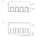
- FIG. 4A and FIG. 4B are diagrams for explaining a manufacturing process of the photoelectric conversion device according to the first embodiment.
- FIG. 5A and FIG. 5B are diagrams for explaining a manufacturing process of the photoelectric conversion device according to the first embodiment.
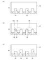
- FIG. 6A and FIG. 6B are diagrams for explaining a manufacturing process of the photoelectric conversion device according to the first embodiment.
- FIG. 7B are diagrams for explaining a manufacturing process of the photoelectric conversion device according to the first embodiment. It is the figure which showed the relationship between the wavelength of light, and the number of photons which permeate
- FIG. 9A to FIG. 9C are diagrams for explaining modifications of the columnar portion in the photoelectric conversion layer according to the first embodiment. It is a figure for demonstrating the modification of the insulation part in the photoelectric converting layer which concerns on 1st Embodiment. It is the figure which showed typically the cross section of the photoelectric conversion apparatus which concerns on 2nd Embodiment. It is the figure which showed typically the cross section of the photoelectric conversion apparatus which concerns on 3rd Embodiment.
- FIG. 14A and FIG. 14B are diagrams for explaining a manufacturing process of the photoelectric conversion device according to the third embodiment.
- FIG. 15A and FIG. 15B are diagrams for explaining a manufacturing process of the photoelectric conversion device according to the third embodiment. It is a figure for demonstrating the manufacturing process of the photoelectric conversion apparatus which concerns on 3rd Embodiment. It is the figure which showed typically the cross section of the photoelectric conversion apparatus which concerns on 4th Embodiment.
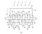
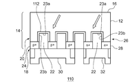
- FIG. 1 is a diagram schematically showing a cross section of the photoelectric conversion device according to the first embodiment. It should be noted that the scales and shapes of each layer and each part shown in the following drawings are set for convenience of explanation, and are not interpreted in a limited manner unless otherwise specified.
- the photoelectric conversion device 10 includes a photoelectric conversion layer 14 having a first semiconductor layer 12 exhibiting a first conductivity type.
- the photoelectric conversion layer 14 is provided so as to surround the plurality of first columnar portions 20 formed on the back surface 18 side opposite to the light receiving surface 16 and the side surfaces of the plurality of first columnar portions 20. And an insulating portion 22.
- the first semiconductor layer 12 is a single-crystal n-type crystalline silicon layer, and has a refractive index of about 3.5 (when the wavelength of light is 1.1 ⁇ m). The refractive index varies depending on the carrier concentration and the wavelength of light.
- the thickness of the photoelectric conversion layer 14 is 100 to 150 ⁇ m.
- the form of the crystalline silicon layer may be single crystal, polycrystalline, microcrystalline, or a mixture.
- the first columnar portion 20 is formed by processing a part of n-type crystalline silicon by a process described later.
- the first columnar portion 20 has a dimension (diameter or diagonal line) shorter than the wavelength of at least part of the light that has passed through the first semiconductor layer 12 when viewed in plan.
- the first columnar portion 20 is formed with a second semiconductor layer 24 having a second conductivity type having a polarity opposite to that of the first semiconductor layer 12.
- the second semiconductor layer 24 is a region (p + layer) having a high concentration of p-type impurities.
- the second semiconductor layer 24 is formed at the end of the first columnar portion 20 opposite to the side facing the first semiconductor layer 12 and has a thickness T1 of about 0.5 ⁇ m to 2 ⁇ m. .5 ⁇ m.
- a depletion layer 25 is formed between the first semiconductor layer 12 that is an n-type substrate and the second semiconductor layer 24 that is a p + layer. Since the depletion layer 25 has a low carrier concentration, the refractive index tends to be higher than that of other adjacent semiconductor layers. Therefore, in the region in the first columnar portion 20, the refractive index difference from the insulating portion 22 surrounding the first columnar portion 20 is further increased, and the light confinement effect is enhanced.
- the depletion layer 25 has a thickness of about 0.5 ⁇ m. The thickness of the depletion layer 25 increases or decreases depending on the carrier concentration.
- the photoelectric conversion layer 14 also has a plurality of second columnar portions 26 formed on the back surface 18 side.
- the side surface of the second columnar part 26 is surrounded by the insulating part 22.
- the second columnar portion 26 has a dimension (diameter or diagonal line) shorter than the wavelength of at least part of the light that has passed through the first semiconductor layer 12 when viewed in plan.
- the second columnar portion 26 is formed with a third semiconductor layer 28 having the same polarity as the first semiconductor layer 12 and showing the first conductivity type.
- the third semiconductor layer 28 is a region (n + layer) having a higher n-type impurity concentration than the first semiconductor layer 12.
- the third semiconductor layer 28 is formed at the end of the second columnar portion 26 on the side opposite to the side facing the first semiconductor layer 12, and the thickness T ⁇ b> 2 is the second semiconductor layer. It is thinner than the thickness T1 of 24 and is about 0.3 ⁇ m to 2.0 ⁇ m.
- the insulating portion 22 is made of a silicon oxide film and has a refractive index of about 1.45. That is, the insulating portion 22 has a refractive index smaller than that of the first columnar portion 20 and the second columnar portion 26.
- the insulating portion 22 may be a single layer film such as a silicon oxide film or a silicon nitride film, or a laminated film thereof.
- the first electrode 30 provided at the tips of the plurality of first columnar portions 20 and the second electrode 32 provided at the tips of the plurality of second columnar portions 26. Is provided on the back surface 18 side of the photoelectric conversion layer 14. Thereby, since the incident light reaches the first semiconductor layer 12 without being blocked by the first electrode 30 and the second electrode 32, compared with the case where the electrode is provided on the light receiving surface 16 side of the photoelectric conversion layer 14. Thus, the power generation efficiency of the photoelectric conversion device 10 is improved.
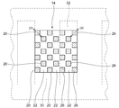
- FIG. 2 is a diagram schematically illustrating a state in which the first columnar portion, the second columnar portion, and the insulating portion of the photoelectric conversion layer illustrated in FIG. 1 are viewed from the back surface side. In FIG. 2, only a part of the photoelectric conversion layer is shown.
- the plurality of first columnar portions 20 are arranged in the upper region of the first electrode 30 at intervals in the vertical and horizontal directions.
- the plurality of second columnar portions 26 are arranged in the upper region of the second electrode 32 at intervals in the vertical and horizontal directions.
- the insulating portions 22 occupy between the columnar portions, and the side surfaces of the columnar portions are completely covered with insulating portions having a refractive index smaller than that of the columnar portions. That is, the side surfaces of the columnar portions are not in contact with each other.
- the first columnar portion 20 is a prism having a quadrangular horizontal cross section.
- the light having a wavelength longer than the diagonal line D1 of the first columnar portion 20 is surrounded by the insulating portion 22 having a refractive index smaller than that of the first columnar portion 20, so that the first columnar portion 20 includes Cannot be propagated. Therefore, as shown in FIG. 1, light having a wavelength longer than the diagonal line D ⁇ b> 1 of the first columnar part 20 among the light that has passed through the first semiconductor layer 12 is reflected by the base 34 of the first columnar part 20. Is done. Therefore, light having a wavelength longer than the diagonal line D1 of the first columnar portion 20 has a substantially long path length in the first semiconductor layer 12 and is easily absorbed by the first semiconductor layer 12.
- the depletion layer 25 is generated in the first columnar portion 20 by providing the second semiconductor layer 24 that is a p + layer in the first columnar portion 20. Since the depletion layer 25 has a relatively high refractive index as compared with the first semiconductor layer 12, the refractive index of the insulating portion 22 surrounding the first columnar portion 20 in the region within the first columnar portion 20. The difference is further increased, and the above effects can be enjoyed more remarkably.
- the depletion layer 25 may reach a region other than the first columnar portion 20 of the first semiconductor layer 12.
- a boundary between the insulating portion 22 and the depletion layer 25 is generated in the entire bottom portion of the insulating portion 22 or a part of the bottom portion, and the difference in refractive index in that portion is increased.
- the presence of a portion having a large difference in refractive index can enhance light reflection at the boundary between the insulating portion 22 and the depletion layer 25.
- the power generation efficiency decreases accordingly.
- the first electrode 30 which is the back electrode is used. Compared with the case of reflecting light, the loss of carriers generated by absorbing light due to recombination is reduced. As a result, the power generation efficiency of the photoelectric conversion device can be increased.
- the second columnar portion 26 is a prism whose horizontal cross section is a quadrangle.
- light having a wavelength longer than the diagonal line D2 of the second columnar portion 26 is surrounded by the insulating portion 22 having a refractive index smaller than that of the second columnar portion 26. Cannot be propagated. Therefore, as shown in FIG. 1, light having a wavelength longer than the diagonal line D ⁇ b> 2 of the second columnar portion 26 among the light that has passed through the first semiconductor layer 12 is reflected by the base portion 36 of the second columnar portion 26. Is done. Therefore, light having a wavelength longer than the diagonal line D ⁇ b> 2 of the second columnar part 26 has a substantially long path length in the first semiconductor layer 12 and is easily absorbed by the first semiconductor layer 12.
- the power generation efficiency decreases accordingly.
- the second electrode 32 since light is reflected on the first semiconductor layer 12 side with respect to the third semiconductor layer 28 that is the n + layer, the second electrode 32 that is the back electrode is used. Compared with the case of reflecting light, the loss of carriers generated by absorbing light due to recombination is reduced. As a result, the power generation efficiency of the photoelectric conversion device can be increased.
- the side surface of the first columnar portion 20 (or the second columnar portion 26) having a relatively large refractive index is surrounded by the insulating portion 22 having a relatively small refractive index. . That is, due to the difference in refractive index between the two, reflection easily occurs on the inner surface of the first columnar portion 20 (or the second columnar portion 26). Therefore, even if light having a wavelength shorter than the diagonal line D1 (or the diagonal line D2) propagates through the first columnar part 20 (or the second columnar part 26), the leakage to the insulating part 22 is suppressed. The As a result, the path length of the light propagating through the first columnar portion 20 (or the second columnar portion 26) is increased, and the light is easily absorbed.
- the length of the diagonal line D1 of the first columnar part 20 is not less than 0.3 ⁇ m and not more than 3 ⁇ m.
- the wavelength of light contained in sunlight is almost included in the range of 0.3 to 3 ⁇ m. Therefore, when the length of the diagonal D1 of the 1st columnar part 20 exceeds 3 micrometers, the light contained in the sunlight which reaches
- the length of the diagonal line D1 of the first columnar part 20 is less than 0.3 ⁇ m, the difficulty of manufacturing the first columnar part 20 increases, but the wavelength of the reflected light out of the light included in the sunlight increases. The light is virtually unchanged. Therefore, there is little need to configure the first columnar portion 20 so that the length of the diagonal line is less than 0.3 ⁇ m. For this reason, the length of the diagonal line D1 of the first columnar portion 20 is set.
- the length of the diagonal D2 of the second columnar portion 26 is preferably 0.3 ⁇ m or more and 3 ⁇ m or less.
- the height of the first columnar portion 20 is 3 ⁇ m or less. Even if light having a wavelength longer than the height of the first columnar part 20 is not reflected by the base 34 of the first columnar part 20 and propagates through the first columnar part 20, it is transmitted without being absorbed. There is a possibility that. Therefore, it is desirable to increase the height of the first columnar portion 20 from the viewpoint of preventing light from being transmitted, but the resistance increases on the contrary. Therefore, by setting the height of the first columnar portion to 3 ⁇ m or less which is not more than the wavelength of light, it is possible to achieve both suppression of light transmission and suppression of increase in resistance.
- the height of the second columnar portion 26 is preferably 3 ⁇ m or less.
- FIG. 3 is an enlarged view of a main part of FIG.
- the insulating portion 22 is a portion other than the first columnar portion 20 and the second columnar portion 26.
- One insulating part 22a is connected to four insulating parts 22b adjacent at four corners.
- the insulating part 22a shown in FIG. 3 preferably has a dimension in the horizontal cross section of 0.3 ⁇ m or more and 3 ⁇ m or less, similarly to the reason for setting the length or diameter of the diagonal line of the columnar part.
- W the dimension of the insulating portion 22a is approximately defined by W ⁇ ⁇ 2.
- each columnar portion has been described as a prism, but the corner of the prism may be rounded, and each columnar portion may be a cylinder.
- the above numerical values set as diagonal lines of a prism may be replaced with the diameter of the cylinder.
- the lengths of all sides on the upper surface do not need to be equal, and the upper surface needs to be square like the first columnar part 20 and the second columnar part 26 in the first embodiment. Absent.
- it may be a prism having a rectangular top surface.
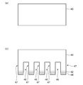
- FIG. 4A and FIG. 4B are diagrams for explaining a manufacturing process of the photoelectric conversion device 10 according to the first embodiment.
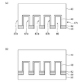
- FIG. 5A and FIG. 5B are diagrams for explaining a manufacturing process of the photoelectric conversion device 10 according to the first embodiment.
- FIG. 6A and FIG. 6B are diagrams for explaining a manufacturing process of the photoelectric conversion device 10 according to the first embodiment.
- FIG. 7A and FIG. 7B are diagrams for explaining a manufacturing process of the photoelectric conversion device 10 according to the first embodiment.
- an n-type crystalline silicon substrate 40 having a thickness of about 10 to 150 ⁇ m is prepared.
- a mask having a predetermined pattern is formed on one surface of the substrate 40, and a silicon oxide film 42 and a silicon nitride film 44 are formed on a portion other than the mask by a plasma CVD method (FIG. 4B).
- the silicon oxide film 42 has a thickness of 20 nm or less
- the silicon nitride film 44 has a thickness of 200 nm or less.
- a part of the substrate 40 is etched using the silicon oxide film 42 and the silicon nitride film 44 as a mask, thereby forming a plurality of grooves 46.
- a plurality of columnar portions 47 are formed with the groove 46 interposed therebetween.
- a silicon oxide film 48 is formed on the inner wall of the groove 46 (see FIG. 5A). Further, a silicon oxide film 50 is formed on the substrate 40 by high density plasma CVD until at least the trench 46 is filled (FIG. 5B). In the present embodiment, the thickness of the silicon oxide film 50 is 2000 nm or less.
- a PSG film 52 is formed on a predetermined region of the etched back surface of the substrate 40 by applying a PSG (Phospho ⁇ ⁇ SilicatenGlass) solution containing phosphorus as an n-type impurity diffusion source by a spin coating method. Further, a BSG (Boron Silicate Glass) solution containing boron as a n-type impurity diffusion source is applied to the surface where the substrate 40 is exposed and the surface of the PSG film 52 by spin coating to form a BSG film 54. (FIG. 6B).
- the PSG film 52 and the BSG film 54 have a thickness of about 200 nm or less.
- the substrate 40 is heat-treated to form diffusion layers 56 and 58 having a high impurity concentration in the columnar portions 47a and 47b (FIG. 7A).
- the photoelectric conversion apparatus 10 is manufactured by removing a part of PSG film
- the electrode material aluminum or copper is preferable.
- the electrode is formed of aluminum, a vapor deposition method is preferable.
- sputtering method and a plating method are suitable.
- the columnar portion 47 a corresponds to the first columnar portion 20.
- the columnar portion 47 b corresponds to the second columnar portion 26.
- the silicon oxide film 48 and the silicon oxide film 50 correspond to the insulating portion 22.
- the diffusion layer 56 corresponds to the second semiconductor layer 24 having a high p-type impurity concentration, and the diffusion layer 58 corresponds to the third semiconductor layer 28 having a high n-type impurity concentration.
- the electrode 60 corresponds to the first electrode 30, and the electrode 62 corresponds to the second electrode 32.
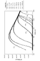
- FIG. 8 is a diagram showing the relationship between the wavelength of light and the number of photons transmitted through a substrate having a predetermined thickness.
- the results of calculation with the substrate thickness changed to 0 ⁇ m, 0.1 ⁇ m, 1 ⁇ m, 10 ⁇ m, 50 ⁇ m, 100 ⁇ m, 150 ⁇ m, 300 ⁇ m, and 10,000 ⁇ m are shown in an overlapping manner.
- the silicon substrate has wavelength dependency in the number of photons to be transmitted.
- the thickness of the silicon substrate is 0 ⁇ m, that is, when there is no light absorption at the substrate, the number of photons per wavelength is as shown in the graph G1 shown in FIG. Further, in the other graphs, the rate of decrease in the transmission number of photons on the short wavelength side is larger than the graph G1. In particular, the tendency becomes more remarkable as the thickness of the silicon substrate increases.
- the thickness of the silicon substrate is 10000 ⁇ m (10 mm), as shown in the graph G2, light having a wavelength of about 1200 nm or more is almost transmitted and not absorbed.
- the longer the wavelength the harder it is to be absorbed by the silicon substrate, while the thicker the silicon substrate, the better the light absorption rate. That is, as the silicon substrate becomes thicker, the upper limit value ⁇ max of the wavelength range of light that is absorbed without difficulty in the silicon substrate also increases. For this reason, the light that needs to be reflected by the above-described columnar portion only needs to be larger than the upper limit value ⁇ max.
- the upper limit value ⁇ max is about 600 nm as shown in the graph G3 shown in FIG. Therefore, if light having a wavelength of 600 nm or more that is not completely absorbed before passing through the silicon substrate is reflected by the region formed by the columnar portion surrounded by the insulating portion, light on the long wavelength side that is difficult to be absorbed The path length is substantially extended, and the overall light absorption rate is improved. That is, when the thickness of the silicon substrate is 10 ⁇ m, the length (or diameter) of the diagonal line of the columnar portion may be 0.6 ⁇ m or less. For the same reason, the dimension of the insulating portion 22a may be 0.6 ⁇ m or less.
- the thickness of the silicon substrate is 50 ⁇ m
- the upper limit value ⁇ max is about 800 nm as shown in the graph G4 shown in FIG. Therefore, the length (or diameter) of the diagonal line of the columnar part may be 0.8 ⁇ m or less.
- the dimension of the insulating portion 22a may be 0.8 ⁇ m or less.
- the upper limit value ⁇ max is about 900 nm as shown in the graph G5 shown in FIG. Therefore, the length (or diameter) of the diagonal line of the columnar part may be 0.9 ⁇ m or less. For the same reason, the dimension of the insulating portion 22a may be 0.9 ⁇ m or less.
- the thickness of the silicon substrate is 150 ⁇ m
- the upper limit value ⁇ max is about 950 nm as shown in the graph G6 shown in FIG. Therefore, the length (or diameter) of the diagonal line of the columnar part may be 0.95 ⁇ m or less.
- the dimension of the insulating portion 22a may be 0.95 ⁇ m or less.
- FIG. 9A to FIG. 9C are diagrams for explaining modifications of the columnar portion in the photoelectric conversion layer according to the first embodiment.
- the first columnar portion 74 and the second columnar portion 76 are both tapered from the center of the substrate toward the surface. Therefore, long wavelength light is more reliably reflected at the base of the columnar part.
- the bottom portion 88a of the insulating portion 88 is preferably formed in a conical or hemispherical shape. Thereby, the light that has passed through the first semiconductor layer 12 is easily reflected by the bottom 88 a of the insulating portion 88.
- the heights of the first columnar portions 92 and 94 and the second columnar portions 96 and 98 are different from each other. Thereby, the light transmitted through the first semiconductor layer 12 is easily reflected in various directions. It should be noted that the height of the columnar part, the length (or diameter) of the diagonal line, the depth and width of the insulating part, and the like may be different in some regions in the plane of the substrate 40. As a result, light is easily reflected in various directions, so that the path length of light can be increased.
- the following effects can be expected by reflection of light at each columnar part.
- light having a long wavelength is reflected at the base of each of the columnar parts.
- Near-field light combines with elementary excitations (phonons and plasmons) in a solid to form polaritons. Or near field light couple
- These states may be higher than the energy of incident light, and light having a wavelength that cannot be photoelectrically converted by the photoelectric conversion layer (semiconductor layer) can be absorbed by the photoelectric conversion layer. As a result, the power generation efficiency of the photoelectric conversion device 10 is improved.
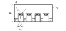
- FIG. 10 is a diagram for explaining a modification of the insulating portion in the photoelectric conversion layer 14 according to the first embodiment.
- nanoparticles 100 are deposited on the bottom side of the groove.
- the nanoparticles 100 are deposited after the silicon oxide film 48 is formed on the inner wall of the groove in the step shown in FIG.
- the nanoparticle 100 is preferably a nanoparticle made of a metal material or an alloy material such as Au, Ag, Cu, Pt, W, Mo, Ni, ZnS, CdSe, Si, or Si coated with Cu on the surface.
- the average particle size of the nanoparticles 100 is not particularly limited as long as the average particle size can be deposited in the groove portion of the insulating portion 22, but may be, for example, 1000 nm or less.
- near-field light is generated when incident light is reflected at the base of the columnar part. Since the near-field light oozes in the vicinity of the reflection point, surface plasmon is likely to be generated on the surface of the nanoparticle 100 when the nanoparticle 100 is deposited on the bottom of the insulating portion 22. For this reason, the power generation efficiency can be improved as described above.
- FIG. 11 is a diagram schematically illustrating a cross section of the photoelectric conversion device according to the second embodiment.
- symbol is attached
- an n layer 112 having the same conductivity type as that of the first semiconductor layer 12 and a high carrier concentration is formed on the bottom 23 a and the side 23 b of the insulating portion 22.
- the n layer 112 is formed so that the carrier concentration is lower than that of the third semiconductor layer 28 to be formed later. Thereby, the recombination of minority carriers on the back surface 18 side as well as the light receiving surface 16 side of the photoelectric conversion device 110 is reduced, and the characteristics of the photoelectric conversion device 110 are improved.
- the n layer 112 is formed by the following method, for example. After the process shown in FIG. 5A, a PSG liquid is applied by a spin coating method to form a PSG film. The PSG film formed at this time is adjusted to have a lower impurity concentration than the PSG film 52 described above. Thereafter, the step shown in FIG. Then, the n layer 112 having a high carrier concentration is formed simultaneously with the diffusion layers 56 and 58 by the heat treatment in the step shown in FIG.
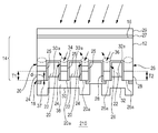
- FIG. 12 is a diagram schematically illustrating a cross section of the photoelectric conversion device according to the third embodiment.
- symbol is attached
- a protective film (passivation film) 27 is laminated on the light receiving surface 16 side of the photoelectric conversion layer 14.
- An antireflection film 29 made of silicon nitride (SiN) is laminated on the protective film 27.
- the photoelectric conversion device 210 In the photoelectric conversion device 210, light having a wavelength longer than the diagonal line of the first columnar portion 20 is reflected by the base 34 of the first columnar portion 20 in the same manner as the photoelectric conversion device 10 according to the first embodiment. The Therefore, light having a wavelength longer than the diagonal line of the first columnar portion 20 has a substantially longer path length in the first semiconductor layer 12 and is easily absorbed by the first semiconductor layer 12. Of the light that has passed through the first semiconductor layer 12, light having a wavelength longer than the diagonal line of the second columnar portion 26 is reflected by the base portion 36 of the second columnar portion 26. Therefore, light having a wavelength longer than the diagonal line of the second columnar portion 26 has a substantially longer path length in the first semiconductor layer 12 and is easily absorbed by the first semiconductor layer 12. Therefore, the photoelectric conversion device 210 can further improve the absorption of light in the semiconductor layer, like the photoelectric conversion device 10 according to the first embodiment.
- the photoelectric conversion device 210 has a first electrode 30 that functions as a first metal wiring layer formed on the surfaces of the first columnar portion 20 and the insulating portion 22.
- the first electrode 30 has a first protruding portion 30 a formed so that a part thereof protrudes toward the first semiconductor layer 12 side from the top portion 20 a of the first columnar portion 20. Yes.
- the first projecting portion 30 a is formed so as to cover the insulating portion 22 between the first columnar portion 20 and the adjacent first columnar portion 20. That is, the first protrusion 30 a constituting a part of the metal wiring is provided so as to surround the side surface in the vicinity of the top portion 20 a of the first columnar portion 20.
- a part of the first columnar portion 20 functions as a waveguide.
- the waveguide reflects light having a wavelength longer than its diagonal or diameter.
- the photoelectric conversion device 210 has a second electrode 32 functioning as a second metal wiring layer formed on the surfaces of the second columnar portion 26 and the insulating portion 22.
- the second electrode 32 has a second protruding portion 32 a formed so that a part thereof protrudes toward the first semiconductor layer 12 side from the top portion 26 a of the second columnar portion 26. Yes.
- the second protruding portion 32 a is formed so as to cover the insulating portion 22 between the second columnar portion 26 and the adjacent second columnar portion 26. That is, the second protrusion 32 a constituting a part of the metal wiring is provided so as to surround the side surface in the vicinity of the top portion 26 a of the second columnar portion 26.
- a part of the second columnar portion 26 functions as a waveguide.
- the waveguide reflects light having a wavelength longer than its diagonal or diameter.
- FIG. 13 is a schematic diagram showing a state where a hole having a diameter d is formed in a metal.
- the shape shown in FIG. 13 is the same structure as the cylindrical waveguide.
- Cutoff frequency v c of the cylindrical waveguide of such a diameter d is expressed by the following equation (1).
- v c 1.841c / ( ⁇ ⁇ d)
- c is the speed of light.
- the diameter (diagonal line) d 0.5 ⁇ m
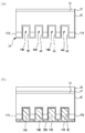
- FIG. 14A and FIG. 14B are diagrams for explaining a manufacturing process of the photoelectric conversion device 210 according to the third embodiment.
- FIG. 15A and FIG. 15B are diagrams for explaining a manufacturing process of the photoelectric conversion device 210 according to the third embodiment.
- FIG. 16 is a diagram for explaining a manufacturing process of the photoelectric conversion device 210 according to the third embodiment.
- an n-type crystalline silicon substrate 40 having a thickness of about 10 to 150 ⁇ m on which diffusion layers 172 and 174 having a high impurity concentration are formed is prepared.
- the diffusion layer 172 corresponds to the second semiconductor layer 24 having a high p-type impurity concentration
- the diffusion layer 174 corresponds to the third semiconductor layer 28 having a high n-type impurity concentration.
- a mask having a predetermined pattern is formed on one surface of the substrate 40, and a silicon oxide film 176 and a resist film 178 are formed by plasma CVD on portions other than the mask.
- a part of the substrate 40 is etched using the silicon oxide film 176 and the resist film 178 as a mask, thereby forming a plurality of holes 146.
- a plurality of columnar portions 47 are formed with the hole 146 interposed therebetween (see FIG. 14B).
- a passivation protective film 27 is formed on the light receiving surface 16 side of the substrate 40, and the back surface 18 side is also covered with the silicon oxide film 48. Thereby, a silicon oxide film 48 is formed on the inner wall of the hole 146 (see FIG. 15A).
- spin-on glass (SOG) 180 is applied to the back surface 18 side of the substrate 40, and the entire hole 146 is filled with the SOG 180 (see FIG. 15B). Further, an antireflection film 29 made of silicon nitride (SiN) is formed on the protective film 27.
- a contact hole 182 is formed using a well-known photolithography technique.
- the etching rates of the silicon oxide film 48 and the SOG 180 are greatly different from each other. Specifically, the etching rate of SOG 180 is about three times the etching rate of silicon oxide film 48. Therefore, when the contact hole 182 is formed, a step 184 is generated between the surface of the silicon oxide film 48 and the surface of the SOG 180.
- the photoelectric conversion device 210 is manufactured (see FIG. 12). Connection reliability with the layer is sufficiently secured.
- the electrode material is preferably aluminum (Al) or copper (Cu). When the electrode is formed of aluminum (Al), a vapor deposition method is preferable. On the other hand, when the electrode is formed of copper (Cu), a sputtering method or a plating method is preferable.
- the columnar portion 47 a corresponds to the first columnar portion 20.
- the columnar portion 47 b corresponds to the second columnar portion 26.
- the hole portion 146 made of the silicon oxide film 48 and the SOG 180 corresponds to the insulating portion 22.
- the diffusion layer 172 corresponds to the second semiconductor layer 24 having a high p-type impurity concentration, and the diffusion layer 174 corresponds to the third semiconductor layer 28 having a high n-type impurity concentration.
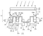
- FIG. 17 is a diagram schematically showing a cross section of the photoelectric conversion device according to the fourth embodiment.
- symbol is attached
- the photoelectric conversion device 310 illustrated in FIG. 17 has substantially the same configuration as the photoelectric conversion device 210 according to the third embodiment, but all of the insulating portion 22 of the photoelectric conversion device 210 illustrated in FIG. 12 is the same as the electrode. It is very different in that it is filled with material.
- the region between the first columnar portions 20 is interposed via the silicon oxide film 48.
- the first protrusion 130a is filled up. That is, the first protrusion 130 a is provided so as to surround the side surface of the second semiconductor layer 24 formed in the first columnar portion 20.
- the first protrusion 130 a is provided so that the tip thereof is located closer to the light receiving surface 16 than the boundary region between the first semiconductor layer 12 and the second semiconductor layer 24.
- the wavelength calculated by the above-described formula (1) among the light reaching the base 34 of the first columnar portion 20 since most of the side surfaces of the first columnar portion 20 are surrounded by the metal material, the wavelength calculated by the above-described formula (1) among the light reaching the base 34 of the first columnar portion 20.
- the light of ⁇ or more cannot be penetrated into the first columnar part 20 and is reflected by the base part 34. Since the base 34 is located closer to the light receiving surface 16 than the second semiconductor layer 24 that is a diffusion layer, the light incident on the second semiconductor layer 24 is further reduced. Therefore, the recombination of minority carriers in the second semiconductor layer 24 is further suppressed, and further improvement in conversion efficiency is expected.
- the second electrode 132 which functions in the same manner as the first electrode 30 of the photoelectric conversion device 210, has a region between the second columnar portions 26 interposed between the silicon oxide films 48. And a second protrusion 132a that is completely filled. That is, the second protruding portion 132 a is provided so as to surround the side surface of the third semiconductor layer 28 formed in the second columnar portion 26. Further, the second projecting portion 132 a is provided so that the tip thereof is located closer to the light receiving surface 16 than the boundary region between the first semiconductor layer 12 and the third semiconductor layer 28.
- the wavelength calculated by the above-described formula (1) among the light reaching the base 36 of the second columnar portion 26 since most of the side surface of the second columnar portion 26 is surrounded by the metal material, the wavelength calculated by the above-described formula (1) among the light reaching the base 36 of the second columnar portion 26.
- the light of ⁇ or more cannot be penetrated into the second columnar part 26 and is reflected by the base part 36. Since the base portion 36 is located closer to the light receiving surface 16 than the third semiconductor layer 28 that is a diffusion layer, the light incident on the third semiconductor layer 28 is further reduced. Therefore, recombination of minority carriers in the third semiconductor layer 28 is further suppressed, and further improvement in conversion efficiency is expected.
- the present invention has been described with reference to the above-described embodiments.
- the present invention is not limited to the above-described embodiments, and the configurations of the embodiments are appropriately combined or replaced. Those are also included in the present invention. Further, it is possible to appropriately change the combination and processing order in each embodiment based on the knowledge of those skilled in the art and to add various modifications such as various design changes to each embodiment. Embodiments to which is added can also be included in the scope of the present invention.
- a photoelectric conversion device in which a columnar portion is provided in P-type crystalline silicon and an n + layer having an opposite conductivity type is provided in the columnar portion may be used.
- the present invention is not limited to this.
- part of the side surfaces of the columnar part (for example, the corners of the columnar part) may be in contact with each other.
- the structure which provided the 1st semiconductor layer so that a columnar part may consist of an insulating part and the side surface may be enclosed may be sufficient. Even in such a case, if the size of the corresponding portion is set to be equal to or smaller than the wavelength of light as in the present embodiment, the same effect as in the present embodiment can be obtained.
- the present invention relates to a photoelectric conversion device suitable for a solar cell.
Landscapes
- Photovoltaic Devices (AREA)
Abstract
光電変換装置10は、一導電型の第1の半導体層12を有する光電変換層14を備える。光電変換層14は、受光面16とは反対側の裏面18側に形成されている複数の第1の柱状部20と、複数の第1の柱状部20の側面を囲むように設けられ、第1の柱状部20よりも屈折率が小さい絶縁部22と、を有する。第1の柱状部20は、第1の半導体層12を通過した光の少なくとも一部の光の波長より短い直径または対角線を有するとともに、第1の半導体層12に対して逆導電型の第2の半導体層24が形成されている。
Description
本発明は、太陽電池に好適な光電変換装置に関する。
従来、光エネルギーを電気エネルギーに変換する光電変換装置として、いわゆる太陽電池の開発が各方面で精力的に行われている。太陽電池は、発生した電気を外部に取り出すための一対の電極が必要であるが、通常は、この電極を太陽光を受光する表面と、その反対側の裏面とに設けている。
しかしながら、受光面側の電極の下部領域には太陽光が入射しないため、その領域は発電に寄与しない。そのため、表面電極は変換効率の低下の一因となる。そこで、一対の電極を裏面に形成した太陽電池が開発されている(特許文献1参照)。
ところで、光を吸収することで電子正孔対を発生する半導体層は、材料費や製造プロセスにおけるコストの低減を考慮すると、より薄いことが望ましい。しかしながら、半導体層が薄すぎる場合、実用的な光の吸収が行われずに光が透過してしまうことになる。
例えば、半導体層が主としてシリコンのような間接遷移型の材料からなる場合、光の吸収効率が悪いため、波長の長い光は吸収されずに半導体層を透過してしまう。特に、シリコンのバンドギャップEgより小さなエネルギーの光(波長が約1100nm以上の光)は発電に寄与しない。
本発明はこうした状況に鑑みてなされたものであり、その目的とするところは、半導体層における光の吸収を更に向上させる技術を提供することにある。
上記課題を解決するために、本発明のある態様の光電変換装置は、一導電型の第1の導電型を示す第1の半導体層を有する光電変換層を備える光電変換装置であって、光電変換層は、受光面とは反対側の裏面側に形成されている複数の第1の柱状部と、第1の柱状部の側面を囲むように設けられ、第1の柱状部よりも屈折率が小さい絶縁部と、を有する。第1の柱状部は、第1の半導体層を通過した光の少なくとも一部の光の波長より短い直径または対角線を有するとともに、第1の半導体層に対して逆導電型の第2の半導体層が形成されている。
本発明によれば、半導体層における光の吸収を更に向上させることができる。
以下、図面を参照しながら、本発明を実施するための形態について詳細に説明する。なお、図面の説明において同一の要素には同一の符号を付し、重複する説明を適宜省略する。
(第1の実施の形態)
図1は、第1の実施の形態に係る光電変換装置の断面を模式的に示した図である。なお、以下の各図に示す各層、各部の縮尺や形状は、説明を容易にするために便宜的に設定されており、特に言及がない限り限定的に解釈されるものではない。
図1は、第1の実施の形態に係る光電変換装置の断面を模式的に示した図である。なお、以下の各図に示す各層、各部の縮尺や形状は、説明を容易にするために便宜的に設定されており、特に言及がない限り限定的に解釈されるものではない。
図1に示すように、第1の実施の形態に係る光電変換装置10は、第1の導電型を示す第1の半導体層12を有する光電変換層14を備える。光電変換層14は、受光面16とは反対側の裏面18側に形成されている複数の第1の柱状部20と、複数の第1の柱状部20の側面を囲むように設けられている絶縁部22と、を有する。
第1の半導体層12は、単結晶のn型結晶シリコン層であり、屈折率は約3.5(光の波長が1.1μmの場合)である。なお、屈折率はキャリア濃度や光の波長によって増減する。また、光電変換層14の厚みは100~150μmである。結晶シリコン層の形態は、単結晶、多結晶、微結晶のいずれか、または、混合物であってもよい。
第1の柱状部20は、後述のプロセスによりn型結晶シリコンの一部が加工されることで形成される。第1の柱状部20は、平面的に見て、第1の半導体層12を通過した光の少なくとも一部の光の波長より短い寸法(直径または対角線)を有する。また、第1の柱状部20は、第1の半導体層12と反対の極性である第2の導電型を示す第2の半導体層24が形成されている。第2の半導体層24は、p型不純物の濃度が高い領域(p+層)である。また、第2の半導体層24は、第1の柱状部20の、第1の半導体層12と対向する側と反対側の端部に形成されており、その厚みT1は約0.5μm~2.5μmである。
なお、第1の柱状部20では、n型基板である第1の半導体層12とp+層である第2の半導体層24との間に空乏層25が形成されている。空乏層25は、キャリア濃度が低いため、隣接する他の半導体層と比較して屈折率が大きくなる傾向にある。そのため、第1の柱状部20内の領域においては、第1の柱状部20を囲む絶縁部22との屈折率差がさらに大きくなり、光の閉じ込め効果が高くなる。空乏層25は、厚みが約0.5μmである。空乏層25の厚みはキャリア濃度に依存して増減する。
光電変換層14は、また、裏面18側に形成されている複数の第2の柱状部26を有している。第2の柱状部26は、側面が絶縁部22により囲まれている。第2の柱状部26は、平面的に見て、第1の半導体層12を通過した光の少なくとも一部の光の波長より短い寸法(直径または対角線)を有する。また、第2の柱状部26は、第1の半導体層12と同じ極性である第1の導電型を示す第3の半導体層28が形成されている。第3の半導体層28は、第1の半導体層12よりもn型不純物の濃度が高い領域(n+層)である。また、第3の半導体層28は、第2の柱状部26の、第1の半導体層12と対向する側と反対側の端部に形成されており、その厚みT2は、第2の半導体層24の厚みT1よりも薄く、約0.3μm~2.0μmである。
絶縁部22は、シリコン酸化膜からなり、屈折率は約1.45である。つまり、絶縁部22は、第1の柱状部20および第2の柱状部26よりも屈折率が小さい。なお、絶縁部22は、シリコン酸化膜やシリコン窒化膜などの単層膜、あるいは、これらの積層膜であってもよい。
なお、光電変換装置10においては、複数の第1の柱状部20の先端に設けられた第1の電極30、および、複数の第2の柱状部26の先端に設けられた第2の電極32が光電変換層14の裏面18側に設けられている。これにより、入射光が第1の電極30および第2の電極32で遮られることなく第1の半導体層12に到達するため、電極を光電変換層14の受光面16側に設けた場合と比較して、光電変換装置10の発電効率が向上する。
次に、第1の柱状部20、第2の柱状部26および絶縁部22の形状や配置について説明する。図2は、図1に示す光電変換層の第1の柱状部、第2の柱状部および絶縁部を裏面側から見た状態を模式的に示した図である。なお、図2では、光電変換層の一部のみを示してある。
図2に示すように、複数の第1の柱状部20は、第1の電極30の上部領域に縦横方向に間隔を空けて配列している。同様に、複数の第2の柱状部26は、第2の電極32の上部領域に縦横方向に間隔を空けて配列している。柱状部同士の間は絶縁部22が占めており、各柱状部の側面は、柱状部より屈折率の小さい絶縁部で完全に覆われている。つまり、各柱状部は、側面が互いに接していない。
第1の柱状部20は、図2に示すように、その水平断面が四角形である角柱である。この場合、第1の柱状部20の対角線D1より長い波長の光は、第1の柱状部20よりも屈折率の小さい絶縁部22で囲まれているので、第1の柱状部20の中には伝播できない。そのため、図1に示すように、第1の半導体層12を通過した光のうち、第1の柱状部20の対角線D1よりも長い波長の光は、第1の柱状部20の基部34で反射される。そのため、第1の柱状部20の対角線D1より長い波長の光は、実質的に第1の半導体層12における行路長が長くなり、第1の半導体層12で吸収されやすくなる。
また、第1の柱状部20内にp+層である第2の半導体層24を設けたことで、第1の柱状部20内に空乏層25が生じる。空乏層25は、第1の半導体層12に比べて相対的に屈折率が大きいので、第1の柱状部20内の領域においては、第1の柱状部20を囲む絶縁部22との屈折率差がさらに大きくなり、上記効果をより顕著に享受することができる。
また、空乏層25は、第1の半導体層12の、第1の柱状部20以外の領域にまで達していてもよい。この場合、絶縁部22の底部全体あるいは底部の一部に絶縁部22と空乏層25との境界が生じ、その部分における屈折率差が大きくなる。このように、屈折率差が大きい部分が存在することで、絶縁部22と空乏層25との境界での光の反射を高めることができる。
なお、半導体層を通過した光がp+層に入射してキャリア(電子正孔対)を発生させても、p+層内ではキャリアはすぐに再結合して消失してしまうため、裏面電極を利用して光を反射させる場合には、その分発電効率が落ちてしまう。第1の実施の形態では、p+層である第2の半導体層24よりも第1の半導体層12側で光を反射させているので、裏面電極である第1の電極30を利用して光を反射させる場合に比べて、光を吸収して発生したキャリアが再結合により消失することが低減される。その結果、光電変換装置の発電効率を高めることができる。
同様に、第2の柱状部26は、図2に示すように、その水平断面が四角形である角柱である。この場合、第2の柱状部26の対角線D2より長い波長の光は、第2の柱状部26よりも屈折率の小さい絶縁部22で囲まれているので、第2の柱状部26の中には伝播できない。そのため、図1に示すように、第1の半導体層12を通過した光のうち、第2の柱状部26の対角線D2よりも長い波長の光は、第2の柱状部26の基部36で反射される。そのため、第2の柱状部26の対角線D2より長い波長の光は、実質的に第1の半導体層12における行路長が長くなり、第1の半導体層12で吸収されやすくなる。
なお、半導体層を通過した光がn+層に入射してキャリア(電子正孔対)を発生させても、n+層内ではキャリアはすぐに再結合して消失してしまうため、裏面電極を利用して光を反射させる場合には、その分発電効率が落ちてしまう。第1の実施の形態では、n+層である第3の半導体層28よりも第1の半導体層12側で光を反射させているので、裏面電極である第2の電極32を利用して光を反射させる場合に比べて、光を吸収して発生したキャリアが再結合により消失することが低減される。その結果、光電変換装置の発電効率を高めることができる。
また、光電変換層14においては、相対的に屈折率の大きい第1の柱状部20(または第2の柱状部26)の側面が、相対的に屈折率の小さい絶縁部22により囲まれている。つまり、両者の屈折率差に起因して、第1の柱状部20(または第2の柱状部26)の内面では反射が起こりやすくなっている。そのため、仮に対角線D1(または対角線D2)よりも短い波長の光が第1の柱状部20(または第2の柱状部26)の内部を伝播しても、絶縁部22に漏れ出ることが抑制される。その結果、第1の柱状部20(または第2の柱状部26)の内部を伝播する光の行路長が長くなり、光が吸収されやすくなる。
第1の柱状部20の対角線D1の長さは、0.3μm以上3μm以下である。太陽光に含まれる光の波長は、0.3~3μmの範囲にほぼ含まれている。そのため、第1の柱状部20の対角線D1の長さが3μmを超えている場合、地上に到達する太陽光に含まれる光を実質的に反射できない。一方、第1の柱状部20の対角線D1の長さが0.3μm未満の場合、第1の柱状部20の製造の難易度が上がるが、太陽光に含まれる光のうち反射される波長の光は実質的に変わらない。そのため、対角線の長さが0.3μm未満となるように第1の柱状部20を構成する必要性は乏しい。このような理由により、第1の柱状部20の対角線D1の長さが設定されている。
同様の理由により、第2の柱状部26の対角線D2の長さは、0.3μm以上3μm以下が好ましい。
次に、各柱状部の高さについて説明する。第1の柱状部20の高さは、3μm以下である。第1の柱状部20の高さより波長の長い光は、仮に第1の柱状部20の基部34で反射せずに第1の柱状部20の内部を伝播しても、吸収されずに透過してしまう可能性がある。そのため、光が透過しないようにするという観点からは第1の柱状部20の高さを高くすることが望ましいが、反対に抵抗が増大してしまう。そこで、第1の柱状部の高さを光の波長以下である3μm以下とすることで、光の透過の抑制と抵抗の増加の抑制とを両立させることが可能となる。
同様の理由により、第2の柱状部26の高さは、3μm以下が好ましい。
次に、絶縁部の形状について説明する。図3は、図2の要部拡大図である。図2、図3に示すように、絶縁部22は、第1の柱状部20および第2の柱状部26以外の部分である。一つの絶縁部22aは、4つの角部で隣接する4つの絶縁部22bとつながっている。図3に示す絶縁部22aは、柱状部の対角線の長さまたは直径の値を設定する理由と同様に、その水平断面での寸法が0.3μm以上3μm以下が好ましい。ここで、隣接して対向する第1の柱状部20(第2の柱状部26)同士の間隔をWと定義すると、絶縁部22aの寸法は、近似的にW×√2で定義される。
以上の説明においては、各柱状部を角柱として説明したが、角柱の角部が丸みを帯びていてもよく、また各柱状部が円柱であってもよい。円柱の場合、角柱の対角線として設定されている上述の数値は、円柱の直径として置き換えてもよい。また、角柱の場合、上面の全ての辺の長さが等しい必要はなく、第1の実施の形態における第1の柱状部20や第2の柱状部26のように上面が正方形である必要もない。例えば、上面が長方形である角柱であってもよい。
次に、第1の実施の形態に係る光電変換装置10の製造方法について説明する。図4(a)、図4(b)は、第1の実施の形態に係る光電変換装置10の製造工程を説明するための図である。図5(a)、図5(b)は、第1の実施の形態に係る光電変換装置10の製造工程を説明するための図である。図6(a)、図6(b)は、第1の実施の形態に係る光電変換装置10の製造工程を説明するための図である。図7(a)、図7(b)は、第1の実施の形態に係る光電変換装置10の製造工程を説明するための図である。
はじめに、図4(a)に示すように、厚みが10~150μm程度のn型結晶シリコンの基板40を用意する。次に、基板40の一方の面上に所定のパターンのマスクをし、マスク以外の部分にシリコン酸化膜42およびシリコン窒化膜44をプラズマCVD法により形成する(図4(b))。第1の実施の形態では、シリコン酸化膜42の厚みは20nm以下、シリコン窒化膜44の厚みは200nm以下である。その後、シリコン酸化膜42およびシリコン窒化膜44をマスクとして基板40の一部をエッチングすることで、複数の溝46が形成される。また、溝46を挟んで複数の柱状部47が形成される。
次に、酸素を用いたドライ酸化を基板40に施すことによりにより、溝46の内壁にシリコン酸化膜48が形成される(図5(a)参照)。更に、高密度プラズマCVD法により、少なくとも溝46が埋まるまでシリコン酸化膜50を基板40上に成膜する(図5(b))。本実施の形態では、シリコン酸化膜50の厚みは2000nm以下である。
次に、反応性イオンエッチング法により基板40の一方の面をエッチバックする(図6(a))。次に、基板40のエッチバックされた面の所定の領域に、n型不純物の拡散源として、リンを含むPSG(Phospho Silicate Glass)液をスピンコート法により塗布しPSG膜52を形成する。更に、基板40が露出している面、および、PSG膜52の表面に、n型不純物の拡散源として、ボロンを含むBSG(Boron Silicate Glass)液をスピンコート法により塗布しBSG膜54を形成する(図6(b))。PSG膜52およびBSG膜54は、約200nm以下の厚みである。
次に、基板40を熱処理することで、不純物濃度の高い拡散層56,58が各柱状部47a,47bに形成される(図7(a))。そして、PSG膜52およびBSG膜54の一部を除去し、電極60,62を形成することで、光電変換装置10が製造される(図7(b))。電極の材料としては、アルミニウムや銅が好ましい。電極をアルミニウムで形成する場合、蒸着法が好適である。一方、電極を銅で形成する場合、スパッタリング法やメッキ法が好適である。
ここで、図7(b)に示す光電変換装置70における各部と、図1に示す光電変換装置10における各部との対応関係を説明する。柱状部47aは、第1の柱状部20に相当する。柱状部47bは、第2の柱状部26に相当する。シリコン酸化膜48およびシリコン酸化膜50は、絶縁部22に相当する。拡散層56は、p型不純物濃度の高い第2の半導体層24に相当し、拡散層58は、n型不純物濃度が高い第3の半導体層28に相当する。電極60は、第1の電極30に相当し、電極62は、第2の電極32に相当する。
次に、柱状部の径についての最適値の範囲について更に検討する。図8は、光の波長と所定の厚みの基板を透過する光子数との関係を示した図である。図8では、基板の厚みを、0μm、0.1μm、1μm、10μm、50μm、100μm、150μm、300μm、10000μmと変化させて計算した結果を重ねて示してある。図8に示すように、シリコン基板は、透過させる光子の数に波長依存性がある。
シリコン基板の厚みが0μmの場合、つまり基板での光の吸収が一切ない場合の波長毎の光子数は、図8に示すグラフG1に示すようになる。そして、グラフG1に対して他のグラフでは短波長側の光子の透過数の減少率が大きい。特に、シリコン基板の厚みが厚くなるほどその傾向は顕著になる。一方、シリコン基板の厚みが10000μm(10mm)の場合、グラフG2に示すように、波長が約1200nm以上の光はほとんど透過し、吸収されない。
このように、波長が長い光ほどシリコン基板で吸収されにくくなる一方、シリコン基板の厚みが厚いほど光の吸収率は向上する。つまり、シリコン基板が厚くなれば、シリコン基板内で無理なく吸収される光の波長域の上限値λmaxも大きくなる。そのため、前述の柱状部で反射させる必要のある光は、上限値λmaxよりも大きければよい。
例えば、シリコン基板の厚みが10μmの場合、図8に示すグラフG3に示すように、上限値λmaxは約600nmである。したがって、シリコン基板を透過するまでに完全には吸収されない600nm以上の波長の光を前述の絶縁部で囲まれた柱状部で構成される領域で反射させれば、吸収されにくい長波長側の光の行路長が実質的に延びることとなり、全体として光の吸収率が向上する。つまり、シリコン基板の厚みが10μmの場合、柱状部の対角線の長さ(または直径)は、0.6μm以下であればよい。同様の理由により、絶縁部22aの寸法は、0.6μm以下であればよい。
同様に、シリコン基板の厚みが50μmの場合、図8に示すグラフG4に示すように、上限値λmaxは約800nmである。したがって、柱状部の対角線の長さ(または直径)は、0.8μm以下であればよい。同様の理由により、絶縁部22aの寸法は、0.8μm以下であればよい。
同様に、シリコン基板の厚みが100μmの場合、図8に示すグラフG5に示すように、上限値λmaxは約900nmである。したがって、柱状部の対角線の長さ(または直径)は、0.9μm以下であればよい。同様の理由により、絶縁部22aの寸法は、0.9μm以下であればよい。
同様に、シリコン基板の厚みが150μmの場合、図8に示すグラフG6に示すように、上限値λmaxは約950nmである。したがって、柱状部の対角線の長さ(または直径)は、0.95μm以下であればよい。同様の理由により、絶縁部22aの寸法は、0.95μm以下であればよい。
なお、シリコン基板の厚みが前述の値以外の場合における柱状部の対角線の長さ(または直径)の上限値は、直線近似や曲線近似により適宜求めればよい。同様に、シリコン基板の厚みが前述の値以外の場合における絶縁部の寸法の上限値は、直線近似や曲線近似により適宜求めればよい。
次に、各柱状部や絶縁部の形状の変形例について説明する。図9(a)~図9(c)は、第1の実施の形態に係る光電変換層における柱状部の変形例を説明するための図である。
図9(a)に示す光電変換層72においては、第1の柱状部74および第2の柱状部76は、いずれも基板中心部から表面に向かってテーパが形成されている。そのため、長波長の光を柱状部の基部でより確実に反射される。
また、図9(b)に示す光電変換装置78は、第1の柱状部80および第2の柱状部82の基部84,86の一部が基板表面に対して斜めに形成されている。換言すると、絶縁部88の底部88aは、円錐状や半球状のように形成されているとよい。これにより、第1の半導体層12を通過した光が絶縁部88の底部88aで反射されやすくなる。
また、図9(c)に示す光電変換層90においては、第1の柱状部92,94および第2の柱状部96,98の高さがそれぞれ異なっている。これにより、第1の半導体層12を透過した光は、様々な方向に反射されやすくなる。なお、柱状部の高さ、対角線の長さ(または直径)、絶縁部の深さ、幅等は、基板40の面内の一部の領域で異なっていてもよい。これにより、様々な方向に光が反射されやすくなるので、光の行路長が長くできる。
なお、各柱状部における光の反射によって次の効果も期待できる。例えば、波長の長い入射光が前述の各柱状部の基部で反射されると、近接場光といわれる光が発生する。近接場光は、固体中の素励起(フォノン、プラズモン)と結合してポラリトンを形成する。または、近接場光は、電子と結合してドレストフォトンを形成する。これらの状態は入射光のエネルギーよりも高くなる可能性があり、光電変換層(半導体層)が光電変換できない波長の光についても、光電変換層で吸収できる。その結果、光電変換装置10の発電効率が向上する。
次に、絶縁部の底部側にナノ粒子を含有させた状態について説明する。図10は、第1の実施の形態に係る光電変換層14における絶縁部の変形例を説明するための図である。
図10に示す絶縁部22は、溝の底部側にナノ粒子100が堆積している。ナノ粒子100は、図5(a)に示す工程で溝の内壁にシリコン酸化膜48を形成した後に、堆積する。ナノ粒子100は、例えば、Au、Ag、Cu、Pt、W、Mo、Ni、ZnS、CdSe、Si、表面にCuコートしたSi、などの金属材料または合金材料からなるナノ粒子が好適である。ナノ粒子100の平均粒径は、絶縁部22の溝部に堆積できる大きさであれば特に限定されないが、例えば、1000nm以下の大きさであってもよい。
前述のように、柱状部の基部で入射光が反射すると、近接場光が発生する。近接場光は、反射点のごく近傍にしみ出すため、絶縁部22の底部にナノ粒子100が堆積していると、ナノ粒子100表面に対して表面プラズモンが発生しやすくなる。このため、前述の通り発電効率を向上させることができる。
(第2の実施の形態)
図11は、第2の実施の形態に係る光電変換装置の断面を模式的に示した図である。なお、前述の各図と同じ構成については同じ符号を付して説明を適宜省略する。図11に示す光電変換装置110は、絶縁部22の底部23aおよび側部23bに、第1の半導体層12と同じ導電型でキャリア濃度の高いn層112が形成されている。なお、n層112は、この後形成される第3の半導体層28よりもキャリア濃度が低くなるように形成されている。これにより、光電変換装置110の受光面16側だけでなく裏面18側における少数キャリアの再結合の低減が図られ、光電変換装置110の特性が向上する。
図11は、第2の実施の形態に係る光電変換装置の断面を模式的に示した図である。なお、前述の各図と同じ構成については同じ符号を付して説明を適宜省略する。図11に示す光電変換装置110は、絶縁部22の底部23aおよび側部23bに、第1の半導体層12と同じ導電型でキャリア濃度の高いn層112が形成されている。なお、n層112は、この後形成される第3の半導体層28よりもキャリア濃度が低くなるように形成されている。これにより、光電変換装置110の受光面16側だけでなく裏面18側における少数キャリアの再結合の低減が図られ、光電変換装置110の特性が向上する。
n層112は、例えば、以下の方法で形成される。図5(a)で示す工程の後に、PSG液をスピンコート法により塗布し、PSG膜を形成する。なお、この際に形成されるPSG膜は、前述のPSG膜52よりも不純物濃度が少なく調整してある。その後、図5(b)で示す工程を行う。そして、図7(a)で示す工程における熱処理により、キャリア濃度の高いn層112は、拡散層56,58と同時に形成される。
(第3の実施の形態)
図12は、第3の実施の形態に係る光電変換装置の断面を模式的に示した図である。なお、前述の各図と同じ構成については同じ符号を付して説明を適宜省略する。
図12は、第3の実施の形態に係る光電変換装置の断面を模式的に示した図である。なお、前述の各図と同じ構成については同じ符号を付して説明を適宜省略する。
図12に示す光電変換装置210は、光電変換層14の受光面16側には、保護膜(パッシベーション膜)27が積層されている。保護膜27の上には窒化シリコン(SiN)からなる反射防止膜29が積層されている。
光電変換装置210は、第1の実施の形態に係る光電変換装置10と同様に、第1の柱状部20の対角線よりも長い波長の光が、第1の柱状部20の基部34で反射される。そのため、第1の柱状部20の対角線より長い波長の光は、実質的に第1の半導体層12における行路長が長くなり、第1の半導体層12で吸収されやすくなる。また、第1の半導体層12を通過した光のうち、第2の柱状部26の対角線よりも長い波長の光は、第2の柱状部26の基部36で反射される。そのため、第2の柱状部26の対角線より長い波長の光は、実質的に第1の半導体層12における行路長が長くなり、第1の半導体層12で吸収されやすくなる。したがって、光電変換装置210は、第1の実施の形態に係る光電変換装置10と同様に、半導体層における光の吸収を更に向上させることができる。
光電変換装置210は、図12に示すように、第1の柱状部20および絶縁部22の表面に形成されている第1の金属配線層として機能する第1の電極30を有する。第1の電極30は、その一部が第1の柱状部20の頂部20aよりも第1の半導体層12側に向かって突出するように形成されている第1の突出部30aを有している。また、第1の突出部30aは、第1の柱状部20と隣接する第1の柱状部20との間の絶縁部22を覆うように形成されている。つまり、金属配線の一部を構成している第1の突出部30aは、第1の柱状部20の頂部20a近傍の側面を囲むように設けられている。
そのため、第1の柱状部20は、その一部が、導波管として機能すると考えられる。導波管は、その対角線や直径よりも長い波長の光を反射する。その結果、第1の半導体層12を通過した光のうち、第1の柱状部20の基部34で反射されずに第1の柱状部20を通過して進んでいく光があっても、少なくともその一部を反射することができる。
このように、第1の柱状部20の頂部20a近傍が金属材料で囲まれるように構成することで、第1の柱状部20を通過してきた光の少なくとも一部が反射され、拡散層である第2の半導体層24に入射する光が減少する。そのため、第2の半導体層24での小数キャリアの再結合が抑制され、変換効率の向上が期待される。
また、光電変換装置210は、図12に示すように、第2の柱状部26および絶縁部22の表面に形成されている第2の金属配線層として機能する第2の電極32を有する。第2の電極32は、その一部が第2の柱状部26の頂部26aよりも第1の半導体層12側に向かって突出するように形成されている第2の突出部32aを有している。また、第2の突出部32aは、第2の柱状部26と隣接する第2の柱状部26との間の絶縁部22を覆うように形成されている。つまり、金属配線の一部を構成している第2の突出部32aは、第2の柱状部26の頂部26a近傍の側面を囲むように設けられている。
そのため、第2の柱状部26は、その一部が、導波管として機能すると考えられる。導波管は、その対角線や直径よりも長い波長の光を反射する。その結果、第1の半導体層12を通過した光のうち、第2の柱状部26の基部36で反射されずに第2の柱状部26を通過して進んでいく光があっても、少なくともその一部を反射することができる。
このように、第2の柱状部26の頂部26a近傍が金属材料で囲まれるように構成することで、第2の柱状部26を通過してきた光の少なくとも一部が反射され、拡散層である第3の半導体層28に入射する光が減少する。そのため、第3の半導体層28での小数キャリアの再結合が抑制され、変換効率の向上が期待される。
次に、各柱状部を導波管とみなした場合の、各柱状部の好適な大きさについて説明する。図13は、金属に直径dの孔が形成されている状態を示す模式図である。図13に示す形状は、円筒形導波管と同じ構造である。
このような直径dの円筒形導波管の遮断周波数vcは以下の式(1)で示される。
vc=1.841c/(π×d)・・・式(1)
ここで、cは光速度である。
vc=1.841c/(π×d)・・・式(1)
ここで、cは光速度である。
したがって、直径(対角線)d=0.5μmの場合、波長λ(=c/vc)は0.85μm程度となり、この波長以上の光は孔に侵入できないことになる。そこで、このような知見に基づいて、各柱状部の直径や対角線の長さを適宜決定するとよい。
次に、第3の実施の形態に係る光電変換装置210の製造方法について説明する。なお、周知の工程や説明については適宜省略する。図14(a)、図14(b)は、第3の実施の形態に係る光電変換装置210の製造工程を説明するための図である。図15(a)、図15(b)は、第3の実施の形態に係る光電変換装置210の製造工程を説明するための図である。図16は、第3の実施の形態に係る光電変換装置210の製造工程を説明するための図である。
はじめに、図14(a)に示すように、不純物濃度の高い拡散層172,174が形成されている、厚みが10~150μm程度のn型結晶シリコンの基板40を用意する。拡散層172は、p型不純物濃度の高い第2の半導体層24に相当し、拡散層174は、n型不純物濃度が高い第3の半導体層28に相当する。次に、基板40の一方の面上に所定のパターンのマスクをし、マスク以外の部分にシリコン酸化膜176およびレジスト膜178をプラズマCVD法により形成する。その後、シリコン酸化膜176およびレジスト膜178をマスクとして基板40の一部をエッチングすることで、複数の孔部146が形成される。また、孔部146を挟んで複数の柱状部47が形成される(図14(b)参照)。
次に、酸素を用いたドライ酸化を基板40に施すことにより、基板40の受光面16側にパッシベーション用の保護膜27が形成されるとともに、裏面18側もシリコン酸化膜48で覆われる。これにより、孔部146の内壁にシリコン酸化膜48が形成される(図15(a)参照)。次に、基板40の裏面18側にスピン・オン・ガラス(SOG)180を塗布し、孔部146全体をSOG180で充填する(図15(b)参照)。また、保護膜27の上に窒化シリコン(SiN)からなる反射防止膜29を形成する。
次に、図16に示すように、周知のフォトリソグラフ技術を用いてコンタクトホール182を形成する。コンタクトホール182を形成する際、シリコン酸化膜48とSOG180とのエッチングレートは互いに大きく異なっている。具体的には、SOG180のエッチングレートは、シリコン酸化膜48のエッチングレートの3倍程度である。したがって、コンタクトホール182を形成しようとすると、シリコン酸化膜48表面とSOG180表面との間で段差184が生じる。
この状態で、電極30,32(図12参照、図16では不図示。)を形成することで、光電変換装置210が製造される(図12参照)が、前述の理由により各電極と各半導体層との接続信頼性は十分確保される。なお、電極の材料としては、アルミニウム(Al)や銅(Cu)が好ましい。電極をアルミニウム(Al)で形成する場合、蒸着法が好適である。一方、電極を銅(Cu)で形成する場合、スパッタリング法やメッキ法が好適である。
ここで、図16に示す光電変換装置220における各部と、図13に示す光電変換装置210における各部との対応関係を説明する。柱状部47aは、第1の柱状部20に相当する。柱状部47bは、第2の柱状部26に相当する。シリコン酸化膜48およびSOG180からなる孔部146は、絶縁部22に相当する。拡散層172は、p型不純物濃度の高い第2の半導体層24に相当し、拡散層174は、n型不純物濃度が高い第3の半導体層28に相当する。
(第4の実施の形態)
図17は、第4の実施の形態に係る光電変換装置の断面を模式的に示した図である。なお、前述の各図と同じ構成については同じ符号を付して説明を適宜省略する。
図17は、第4の実施の形態に係る光電変換装置の断面を模式的に示した図である。なお、前述の各図と同じ構成については同じ符号を付して説明を適宜省略する。
図17に示す光電変換装置310は、第3の実施の形態に係る光電変換装置210とほぼ同様の構成であるが、図12に示す光電変換装置210の絶縁部22の部分が全て電極と同じ材料で充填されている点が大きく異なる。
つまり、光電変換装置210の第1の電極30と同様に機能する第4の実施の形態に係る第1の電極130は、第1の柱状部20同士の間の領域をシリコン酸化膜48を介して全て充填する第1の突出部130aを有している。つまり、第1の突出部130aは、第1の柱状部20に形成されている第2の半導体層24の側面を囲むように設けられている。また、第1の突出部130aは、その先端が、第1の半導体層12と第2の半導体層24との境界領域よりも受光面16側に位置するように設けられている。
これにより、第1の柱状部20の側面のほとんどが金属材料で囲まれているため、第1の柱状部20の基部34に到達した光のうち、前述の式(1)で算出される波長λ以上の光は第1の柱状部20に侵入できずに基部34で反射されることになる。基部34は、拡散層である第2の半導体層24よりも受光面16側に位置するため、第2の半導体層24に入射する光が更に減少する。そのため、第2の半導体層24での小数キャリアの再結合が更に抑制され、変換効率の更なる向上が期待される。
また、光電変換装置210の第1の電極30と同様に機能する第4の実施の形態に係る第2の電極132は、第2の柱状部26同士の間の領域をシリコン酸化膜48を介して全て充填する第2の突出部132aを有している。つまり、第2の突出部132aは、第2の柱状部26に形成されている第3の半導体層28の側面を囲むように設けられている。また、第2の突出部132aは、その先端が、第1の半導体層12と第3の半導体層28との境界領域よりも受光面16側に位置するように設けられている。
これにより、第2の柱状部26の側面のほとんどが金属材料で囲まれているため、第2の柱状部26の基部36に到達した光のうち、前述の式(1)で算出される波長λ以上の光は第2の柱状部26に侵入できずに基部36で反射されることになる。基部36は、拡散層である第3の半導体層28よりも受光面16側に位置するため、第3の半導体層28に入射する光が更に減少する。そのため、第3の半導体層28での小数キャリアの再結合が更に抑制され、変換効率の更なる向上が期待される。
以上、本発明を上述の各実施の形態を参照して説明したが、本発明は上述の各実施の形態に限定されるものではなく、各実施の形態の構成を適宜組み合わせたものや置換したものについても本発明に含まれるものである。また、当業者の知識に基づいて各実施の形態における組合せや処理の順番を適宜組み替えることや各種の設計変更等の変形を各実施の形態に対して加えることも可能であり、そのような変形が加えられた実施の形態も本発明の範囲に含まれうる。
具体的には、P型結晶シリコンに柱状部を設け、この柱状部に逆の導電型のn+層を設けた光電変換装置としてもよい。
また、本実施の形態では、各柱状部の側面が互いに接していない例を示したが、これに限られない。例えば、柱状部の側面の一部(例えば、柱状部の角同士)が接してつながっていてもよい。また、柱状部が絶縁部からなり、その側面を囲むように第1の半導体層を設けた構成であってもよい。こうした場合にも、対応する部分の寸法を本実施の形態のように光の波長以下に設定すれば、本実施の形態と同様の効果を享受することができる。
10 光電変換装置、 12 第1の半導体層、 14 光電変換層、 16 受光面、 18 裏面、 20 第1の柱状部、 22 絶縁部、 23a 底部、 23b 側部、 24 第2の半導体層、 26 第2の柱状部、 28 第3の半導体層、 30 第1の電極、 32 第2の電極、 34,36 基部、 40 基板、 100 ナノ粒子。
本発明は、太陽電池に好適な光電変換装置に関する。
Claims (11)
- 一導電型の第1の半導体層を有する光電変換層を備える光電変換装置であって、
前記光電変換層は、
受光面とは反対側の裏面側に形成されている複数の第1の柱状部と、
前記第1の柱状部の側面を囲むように設けられ、前記第1の柱状部よりも屈折率が小さい絶縁部と、を有し、
前記第1の柱状部は、前記第1の半導体層を通過した光の少なくとも一部の光の波長より短い直径または対角線を有するとともに、前記第1の半導体層に対して逆導電型の第2の半導体層が形成されていることを特徴とする光電変換装置。 - 前記第1の柱状部の直径または対角線は、0.3μm以上3μm以下であることを特徴とする請求項1に記載の光電変換装置。
- 前記絶縁部は、隣接して対向する前記第1の柱状部同士の間隔をWとした場合に、寸法W×√2の値が前記第1の半導体層を通過した光の少なくとも一部の光の波長より短くなるように、構成されていることを特徴とする請求項1または2に記載の光電変換装置。
- 前記第1の柱状部および前記絶縁部の表面に形成されている第1の金属配線層を更に有し、
前記第1の金属配線層は、その一部が前記第1の柱状部の頂部よりも前記第1の半導体層側に向かって突出するように形成されている第1の突出部を有していることを特徴とする請求項1乃至3のいずれか1項に記載の光電変換装置。 - 前記第1の突出部は、前記第1の柱状部に形成されている前記第2の半導体層の側面を囲むように設けられていることを特徴とする請求項4に記載の光電変換装置。
- 前記第1の突出部は、その先端が、前記第1の半導体層と前記第2の半導体層との境界領域よりも受光面側に位置するように設けられていることを特徴とする請求項4または5に記載の光電変換装置。
- 前記光電変換層は、
受光面とは反対側の裏面側に形成されている複数の第2の柱状部と、
前記第2の柱状部の側面を囲むように設けられ、前記第2の柱状部よりも屈折率が小さい絶縁部と、を有し、
前記第2の柱状部は、前記第1の半導体層を通過した光の少なくとも一部の光の波長より短い直径または対角線を有するとともに、前記第1の半導体層と同じ一導電型の第3の半導体層が形成されていることを特徴とする請求項1乃至6のいずれか1項に記載の光電変換装置。 - 前記第2の柱状部の対角線の長さまたは直径は、0.3μm以上3μm以下であることを特徴とする請求項7に記載の光電変換装置。
- 前記第2の柱状部および前記絶縁部の表面に形成されている第2の金属配線層を更に有し、
前記第2の金属配線層は、その一部が前記第2の柱状部の頂部よりも前記第1の半導体層側に向かって突出するように形成されている第2の突出部を有していることを特徴とする請求項7または8に記載の光電変換装置。 - 前記第2の突出部は、前記第2の柱状部に形成されている前記第3の半導体層の側面を囲むように設けられていることを特徴とする請求項9に記載の光電変換装置。
- 前記第2の突出部は、その先端が、前記第1の半導体層と前記第3の半導体層との境界領域よりも受光面側に位置するように設けられていることを特徴とする請求項9または10に記載の光電変換装置。
Applications Claiming Priority (2)
| Application Number | Priority Date | Filing Date | Title |
|---|---|---|---|
| JP2011042402A JP2014096393A (ja) | 2011-02-28 | 2011-02-28 | 光電変換装置 |
| JP2011-042402 | 2011-02-28 |
Publications (1)
| Publication Number | Publication Date |
|---|---|
| WO2012117469A1 true WO2012117469A1 (ja) | 2012-09-07 |
Family
ID=46757439
Family Applications (1)
| Application Number | Title | Priority Date | Filing Date |
|---|---|---|---|
| PCT/JP2011/006077 Ceased WO2012117469A1 (ja) | 2011-02-28 | 2011-10-31 | 光電変換装置 |
Country Status (2)
| Country | Link |
|---|---|
| JP (1) | JP2014096393A (ja) |
| WO (1) | WO2012117469A1 (ja) |
Cited By (1)
| Publication number | Priority date | Publication date | Assignee | Title |
|---|---|---|---|---|
| WO2014080505A1 (ja) * | 2012-11-22 | 2014-05-30 | 株式会社日立製作所 | 太陽電池セル |
Citations (1)
| Publication number | Priority date | Publication date | Assignee | Title |
|---|---|---|---|---|
| JP2006203056A (ja) * | 2005-01-21 | 2006-08-03 | Toyota Motor Corp | 光電変換素子 |
-
2011
- 2011-02-28 JP JP2011042402A patent/JP2014096393A/ja not_active Withdrawn
- 2011-10-31 WO PCT/JP2011/006077 patent/WO2012117469A1/ja not_active Ceased
Patent Citations (1)
| Publication number | Priority date | Publication date | Assignee | Title |
|---|---|---|---|---|
| JP2006203056A (ja) * | 2005-01-21 | 2006-08-03 | Toyota Motor Corp | 光電変換素子 |
Cited By (1)
| Publication number | Priority date | Publication date | Assignee | Title |
|---|---|---|---|---|
| WO2014080505A1 (ja) * | 2012-11-22 | 2014-05-30 | 株式会社日立製作所 | 太陽電池セル |
Also Published As
| Publication number | Publication date |
|---|---|
| JP2014096393A (ja) | 2014-05-22 |
Similar Documents
| Publication | Publication Date | Title |
|---|---|---|
| CN101438419B (zh) | 光电二极管、用于制造这种光电二极管的方法、光学通信设备和光学互连模块 | |
| CN100557826C (zh) | 雪崩光电二极管 | |
| US8467637B2 (en) | Waveguide path coupling-type photodiode | |
| JP5282887B2 (ja) | フォトダイオード、光通信デバイスおよび光インタコネクションモジュール | |
| JP5687765B2 (ja) | 太陽電池 | |
| CN102881761B (zh) | Apd红外探测器及其制作方法 | |
| JP5715891B2 (ja) | 光電変換装置 | |
| CN111640813A (zh) | 一种宽光谱高吸收太阳能电池 | |
| JP5123830B2 (ja) | 反射防止膜、反射防止膜の製造方法、及び反射防止膜を用いた半導体装置 | |
| JP2013191704A (ja) | 受光素子 | |
| CN114335207B (zh) | 一种基于双层亚波长光栅的锗硅光电探测器 | |
| WO2012169123A1 (ja) | 光電変換素子 | |
| TW201327870A (zh) | 太陽能電池的製備方法 | |
| CN101232057B (zh) | 雪崩光电二极管 | |
| JP2014096393A (ja) | 光電変換装置 | |
| US20150179843A1 (en) | Photovoltaic device | |
| WO2025130233A1 (zh) | 适用于非偏振光的等离激元电极光电探测器 | |
| CN115101609B (zh) | 一种基于定向耦合器的锗硅光电探测器 | |
| TWI482295B (zh) | 太陽能電池 | |
| CN113284964B (zh) | 一种导模光电探测器 | |
| JP2013074203A (ja) | 光電変換装置 | |
| CN119153558A (zh) | 一种光电探测器及其制备方法 | |
| JP5412376B2 (ja) | 太陽電池 | |
| KR101575854B1 (ko) | 태양전지용 웨이퍼 구조체 및 이의 제조 방법 | |
| JP2012004497A (ja) | 薄膜太陽電池およびその製造方法 |
Legal Events
| Date | Code | Title | Description |
|---|---|---|---|
| 121 | Ep: the epo has been informed by wipo that ep was designated in this application |
Ref document number: 11859847 Country of ref document: EP Kind code of ref document: A1 |
|
| NENP | Non-entry into the national phase |
Ref country code: DE |
|
| 122 | Ep: pct application non-entry in european phase |
Ref document number: 11859847 Country of ref document: EP Kind code of ref document: A1 |
|
| NENP | Non-entry into the national phase |
Ref country code: JP |