WO2012114940A1 - 新規錯体化合物、及びその利用 - Google Patents
新規錯体化合物、及びその利用 Download PDFInfo
- Publication number
- WO2012114940A1 WO2012114940A1 PCT/JP2012/053392 JP2012053392W WO2012114940A1 WO 2012114940 A1 WO2012114940 A1 WO 2012114940A1 JP 2012053392 W JP2012053392 W JP 2012053392W WO 2012114940 A1 WO2012114940 A1 WO 2012114940A1
- Authority
- WO
- WIPO (PCT)
- Prior art keywords
- atom
- general formula
- carbon atoms
- complex compound
- hydrocarbon group
- Prior art date
- Legal status (The legal status is an assumption and is not a legal conclusion. Google has not performed a legal analysis and makes no representation as to the accuracy of the status listed.)
- Ceased
Links
- 0 *CCCC1CCCC1 Chemical compound *CCCC1CCCC1 0.000 description 2
Images







Classifications
-
- C—CHEMISTRY; METALLURGY
- C09—DYES; PAINTS; POLISHES; NATURAL RESINS; ADHESIVES; COMPOSITIONS NOT OTHERWISE PROVIDED FOR; APPLICATIONS OF MATERIALS NOT OTHERWISE PROVIDED FOR
- C09K—MATERIALS FOR MISCELLANEOUS APPLICATIONS, NOT PROVIDED FOR ELSEWHERE
- C09K11/00—Luminescent materials, e.g. electroluminescent or chemiluminescent
- C09K11/06—Luminescent materials, e.g. electroluminescent or chemiluminescent containing organic luminescent materials
-
- C—CHEMISTRY; METALLURGY
- C07—ORGANIC CHEMISTRY
- C07F—ACYCLIC, CARBOCYCLIC OR HETEROCYCLIC COMPOUNDS CONTAINING ELEMENTS OTHER THAN CARBON, HYDROGEN, HALOGEN, OXYGEN, NITROGEN, SULFUR, SELENIUM OR TELLURIUM
- C07F15/00—Compounds containing elements of Groups 8, 9, 10 or 18 of the Periodic Table
- C07F15/0006—Compounds containing elements of Groups 8, 9, 10 or 18 of the Periodic Table compounds of the platinum group
- C07F15/0033—Iridium compounds
-
- H—ELECTRICITY
- H05—ELECTRIC TECHNIQUES NOT OTHERWISE PROVIDED FOR
- H05B—ELECTRIC HEATING; ELECTRIC LIGHT SOURCES NOT OTHERWISE PROVIDED FOR; CIRCUIT ARRANGEMENTS FOR ELECTRIC LIGHT SOURCES, IN GENERAL
- H05B33/00—Electroluminescent light sources
- H05B33/12—Light sources with substantially two-dimensional [2D] radiating surfaces
- H05B33/14—Light sources with substantially two-dimensional [2D] radiating surfaces characterised by the chemical or physical composition or the arrangement of the electroluminescent material, or by the simultaneous addition of the electroluminescent material in or onto the light source
-
- H—ELECTRICITY
- H10—SEMICONDUCTOR DEVICES; ELECTRIC SOLID-STATE DEVICES NOT OTHERWISE PROVIDED FOR
- H10K—ORGANIC ELECTRIC SOLID-STATE DEVICES
- H10K85/00—Organic materials used in the body or electrodes of devices covered by this subclass
- H10K85/30—Coordination compounds
- H10K85/341—Transition metal complexes, e.g. Ru(II)polypyridine complexes
- H10K85/342—Transition metal complexes, e.g. Ru(II)polypyridine complexes comprising iridium
-
- C—CHEMISTRY; METALLURGY
- C09—DYES; PAINTS; POLISHES; NATURAL RESINS; ADHESIVES; COMPOSITIONS NOT OTHERWISE PROVIDED FOR; APPLICATIONS OF MATERIALS NOT OTHERWISE PROVIDED FOR
- C09K—MATERIALS FOR MISCELLANEOUS APPLICATIONS, NOT PROVIDED FOR ELSEWHERE
- C09K2211/00—Chemical nature of organic luminescent or tenebrescent compounds
- C09K2211/10—Non-macromolecular compounds
- C09K2211/1003—Carbocyclic compounds
- C09K2211/1007—Non-condensed systems
-
- C—CHEMISTRY; METALLURGY
- C09—DYES; PAINTS; POLISHES; NATURAL RESINS; ADHESIVES; COMPOSITIONS NOT OTHERWISE PROVIDED FOR; APPLICATIONS OF MATERIALS NOT OTHERWISE PROVIDED FOR
- C09K—MATERIALS FOR MISCELLANEOUS APPLICATIONS, NOT PROVIDED FOR ELSEWHERE
- C09K2211/00—Chemical nature of organic luminescent or tenebrescent compounds
- C09K2211/10—Non-macromolecular compounds
- C09K2211/1003—Carbocyclic compounds
- C09K2211/1011—Condensed systems
-
- C—CHEMISTRY; METALLURGY
- C09—DYES; PAINTS; POLISHES; NATURAL RESINS; ADHESIVES; COMPOSITIONS NOT OTHERWISE PROVIDED FOR; APPLICATIONS OF MATERIALS NOT OTHERWISE PROVIDED FOR
- C09K—MATERIALS FOR MISCELLANEOUS APPLICATIONS, NOT PROVIDED FOR ELSEWHERE
- C09K2211/00—Chemical nature of organic luminescent or tenebrescent compounds
- C09K2211/10—Non-macromolecular compounds
- C09K2211/1003—Carbocyclic compounds
- C09K2211/1014—Carbocyclic compounds bridged by heteroatoms, e.g. N, P, Si or B
-
- C—CHEMISTRY; METALLURGY
- C09—DYES; PAINTS; POLISHES; NATURAL RESINS; ADHESIVES; COMPOSITIONS NOT OTHERWISE PROVIDED FOR; APPLICATIONS OF MATERIALS NOT OTHERWISE PROVIDED FOR
- C09K—MATERIALS FOR MISCELLANEOUS APPLICATIONS, NOT PROVIDED FOR ELSEWHERE
- C09K2211/00—Chemical nature of organic luminescent or tenebrescent compounds
- C09K2211/10—Non-macromolecular compounds
- C09K2211/1018—Heterocyclic compounds
- C09K2211/1022—Heterocyclic compounds bridged by heteroatoms, e.g. N, P, Si or B
-
- C—CHEMISTRY; METALLURGY
- C09—DYES; PAINTS; POLISHES; NATURAL RESINS; ADHESIVES; COMPOSITIONS NOT OTHERWISE PROVIDED FOR; APPLICATIONS OF MATERIALS NOT OTHERWISE PROVIDED FOR
- C09K—MATERIALS FOR MISCELLANEOUS APPLICATIONS, NOT PROVIDED FOR ELSEWHERE
- C09K2211/00—Chemical nature of organic luminescent or tenebrescent compounds
- C09K2211/10—Non-macromolecular compounds
- C09K2211/1018—Heterocyclic compounds
- C09K2211/1025—Heterocyclic compounds characterised by ligands
- C09K2211/1029—Heterocyclic compounds characterised by ligands containing one nitrogen atom as the heteroatom
-
- C—CHEMISTRY; METALLURGY
- C09—DYES; PAINTS; POLISHES; NATURAL RESINS; ADHESIVES; COMPOSITIONS NOT OTHERWISE PROVIDED FOR; APPLICATIONS OF MATERIALS NOT OTHERWISE PROVIDED FOR
- C09K—MATERIALS FOR MISCELLANEOUS APPLICATIONS, NOT PROVIDED FOR ELSEWHERE
- C09K2211/00—Chemical nature of organic luminescent or tenebrescent compounds
- C09K2211/10—Non-macromolecular compounds
- C09K2211/1018—Heterocyclic compounds
- C09K2211/1025—Heterocyclic compounds characterised by ligands
- C09K2211/1029—Heterocyclic compounds characterised by ligands containing one nitrogen atom as the heteroatom
- C09K2211/1033—Heterocyclic compounds characterised by ligands containing one nitrogen atom as the heteroatom with oxygen
-
- C—CHEMISTRY; METALLURGY
- C09—DYES; PAINTS; POLISHES; NATURAL RESINS; ADHESIVES; COMPOSITIONS NOT OTHERWISE PROVIDED FOR; APPLICATIONS OF MATERIALS NOT OTHERWISE PROVIDED FOR
- C09K—MATERIALS FOR MISCELLANEOUS APPLICATIONS, NOT PROVIDED FOR ELSEWHERE
- C09K2211/00—Chemical nature of organic luminescent or tenebrescent compounds
- C09K2211/10—Non-macromolecular compounds
- C09K2211/1018—Heterocyclic compounds
- C09K2211/1025—Heterocyclic compounds characterised by ligands
- C09K2211/1029—Heterocyclic compounds characterised by ligands containing one nitrogen atom as the heteroatom
- C09K2211/1037—Heterocyclic compounds characterised by ligands containing one nitrogen atom as the heteroatom with sulfur
-
- C—CHEMISTRY; METALLURGY
- C09—DYES; PAINTS; POLISHES; NATURAL RESINS; ADHESIVES; COMPOSITIONS NOT OTHERWISE PROVIDED FOR; APPLICATIONS OF MATERIALS NOT OTHERWISE PROVIDED FOR
- C09K—MATERIALS FOR MISCELLANEOUS APPLICATIONS, NOT PROVIDED FOR ELSEWHERE
- C09K2211/00—Chemical nature of organic luminescent or tenebrescent compounds
- C09K2211/10—Non-macromolecular compounds
- C09K2211/1018—Heterocyclic compounds
- C09K2211/1025—Heterocyclic compounds characterised by ligands
- C09K2211/1044—Heterocyclic compounds characterised by ligands containing two nitrogen atoms as heteroatoms
-
- C—CHEMISTRY; METALLURGY
- C09—DYES; PAINTS; POLISHES; NATURAL RESINS; ADHESIVES; COMPOSITIONS NOT OTHERWISE PROVIDED FOR; APPLICATIONS OF MATERIALS NOT OTHERWISE PROVIDED FOR
- C09K—MATERIALS FOR MISCELLANEOUS APPLICATIONS, NOT PROVIDED FOR ELSEWHERE
- C09K2211/00—Chemical nature of organic luminescent or tenebrescent compounds
- C09K2211/10—Non-macromolecular compounds
- C09K2211/1018—Heterocyclic compounds
- C09K2211/1025—Heterocyclic compounds characterised by ligands
- C09K2211/1088—Heterocyclic compounds characterised by ligands containing oxygen as the only heteroatom
-
- C—CHEMISTRY; METALLURGY
- C09—DYES; PAINTS; POLISHES; NATURAL RESINS; ADHESIVES; COMPOSITIONS NOT OTHERWISE PROVIDED FOR; APPLICATIONS OF MATERIALS NOT OTHERWISE PROVIDED FOR
- C09K—MATERIALS FOR MISCELLANEOUS APPLICATIONS, NOT PROVIDED FOR ELSEWHERE
- C09K2211/00—Chemical nature of organic luminescent or tenebrescent compounds
- C09K2211/10—Non-macromolecular compounds
- C09K2211/1018—Heterocyclic compounds
- C09K2211/1025—Heterocyclic compounds characterised by ligands
- C09K2211/1092—Heterocyclic compounds characterised by ligands containing sulfur as the only heteroatom
-
- C—CHEMISTRY; METALLURGY
- C09—DYES; PAINTS; POLISHES; NATURAL RESINS; ADHESIVES; COMPOSITIONS NOT OTHERWISE PROVIDED FOR; APPLICATIONS OF MATERIALS NOT OTHERWISE PROVIDED FOR
- C09K—MATERIALS FOR MISCELLANEOUS APPLICATIONS, NOT PROVIDED FOR ELSEWHERE
- C09K2211/00—Chemical nature of organic luminescent or tenebrescent compounds
- C09K2211/18—Metal complexes
- C09K2211/185—Metal complexes of the platinum group, i.e. Os, Ir, Pt, Ru, Rh or Pd
-
- H—ELECTRICITY
- H10—SEMICONDUCTOR DEVICES; ELECTRIC SOLID-STATE DEVICES NOT OTHERWISE PROVIDED FOR
- H10K—ORGANIC ELECTRIC SOLID-STATE DEVICES
- H10K2101/00—Properties of the organic materials covered by group H10K85/00
- H10K2101/10—Triplet emission
-
- H—ELECTRICITY
- H10—SEMICONDUCTOR DEVICES; ELECTRIC SOLID-STATE DEVICES NOT OTHERWISE PROVIDED FOR
- H10K—ORGANIC ELECTRIC SOLID-STATE DEVICES
- H10K50/00—Organic light-emitting devices
- H10K50/10—OLEDs or polymer light-emitting diodes [PLED]
- H10K50/11—OLEDs or polymer light-emitting diodes [PLED] characterised by the electroluminescent [EL] layers
Definitions
- the present invention relates to a novel complex compound and use of the complex compound. More specifically, the present invention relates to a light emitting element including the complex compound.
- OLEDs Organic Light-emitting elements
- OLEDs Organic Light-Emitting Devices
- metal complex that emits phosphorescence as a light-emitting material have attracted attention because of their significantly higher emission efficiency than fluorescent light-emitting materials.
- Non-Patent Document 1 Non-Patent Documents 1 to 4.
- Patent Document 1 Although the iridium complex disclosed in Patent Document 1 shows sufficient light emission characteristics in practical use, there is still room for improvement.
- the iridium complexes disclosed in Non-Patent Documents 1 to 4 have a dipyridylamine (DpaH) ligand.
- DpaH dipyridylamine
- EL organic electroluminescence
- all of the iridium complexes disclosed in Non-Patent Documents 1 to 4 are ionic complexes, and there is a problem that even when sublimation is attempted, the complex is decomposed before sublimation. That is, sublimation of these iridium complexes is impossible, and it is impossible to produce an EL device by vacuum deposition using these iridium complexes. Therefore, these iridium complexes could not be used as EL materials.
- the present invention has been made in view of the above-mentioned problems, and an object of the present invention is to provide a novel complex compound that can be vacuum-deposited and has excellent luminescent properties.
- the inventors of the present application have conducted intensive studies to solve the above problems. As a result, it was found that by using an auxiliary ligand having a specific structure, a complex compound exhibiting excellent phosphorescence emission characteristics, neutral and excellent in thermal stability can be obtained, and the present invention is completed. It came to.
- the complex compound according to the present invention is characterized in that it is a complex compound represented by the following general formula (1) in order to solve the above problems. According to this, since it is a neutral complex and excellent in thermal stability, vacuum deposition is possible, and it is possible to provide a novel complex compound excellent in light emission characteristics such as energy efficiency.
- C ⁇ N (location indicated by A1) represents a cyclometalated ligand
- N ⁇ N (location indicated by A2) is the following general formula (2) or the following general formula (3).
- M represents a transition metal atom.
- M and n are both integers of 1 or more, and the sum of m and n is less than or equal to the maximum number of ligands that can coordinate to M.
- R1 to R8 each independently represent a hydrogen atom; a halogen atom; a silyl group; an alkylsilyl group; or a hydrocarbon group having 1 to 10 carbon atoms; At least one hydrogen contained in the hydrogen group may be substituted with a halogen atom.
- the hydrocarbon group contains two or more carbon atoms, a part of the carbon atom is substituted with a sulfur atom or an oxygen atom.
- the hydrocarbon groups may be linked to each other to form a ring. * In general formulas (2) and (3), * represents coordination to M.
- the light emitting method according to the present invention is characterized in that a voltage is applied to the complex compound to cause the complex compound to emit light.
- a light-emitting element includes a pair of electrodes and a light-emitting layer including a light-emitting material disposed between the pair of electrodes, and the light-emitting layer includes the complex compound. It is characterized by becoming. According to this, it is possible to provide a light emitting element that exhibits practically sufficient light emission characteristics.
- the complex compound and its use according to the present invention is a neutral complex and excellent in thermal stability, so that vacuum deposition is possible, and a novel complex compound excellent in light emission characteristics such as energy efficiency and the complex compound are used.
- the light emitting method and the light emitting element can be provided.
- FIG. 1 is a diagram showing the structure of a complex compound according to the present invention.
- (A) in FIG. 1 shows the single crystal structure of the complex compound according to the present invention
- (b) in FIG. 3 shows crystal packing of a complex compound according to the invention.
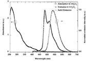
- FIG. 2 is a graph showing the UV-Vis absorption spectrum and PL spectrum of the complex compound according to the present invention observed in degassed dichloromethane or in a solid phase state.
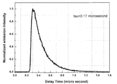
- FIG. 3 is a graph showing the results of measuring the emission lifetime of the complex compound according to the present invention.
- FIG. 4 is a diagram showing a cyclic voltammogram of the complex compound according to the present invention.
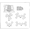
- FIG. 5 is an explanatory view showing the structure of the organic light emitting devices OLEDs I to IV (Device I to IV) according to the present invention and the chemical structure of the material constituting the organic light emitting device.
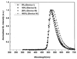
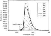
- FIG. 6 is a graph showing EL spectra of OLEDs I to IV (Device I to IV) when a driving voltage of 9 V is applied.
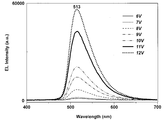
- FIG. 7 is a graph showing EL spectra of OLEDsI when different driving voltages are applied.
- FIG. 8 is a graph showing measurement results of luminance-voltage characteristics and current density-voltage characteristics of OLEDs I to IV (Device I to IV).
- FIG. 6 is a graph showing EL spectra of OLEDs I to IV (Device I to IV) when a driving voltage of 9 V is applied.
- FIG. 7 is a graph showing EL spectra of OLEDsI when different driving voltages are applied.
- FIG. 8 is a graph showing measurement results of luminance-voltage characteristics and current
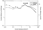
- FIG. 9 is a graph showing the relationship between current density-energy efficiency and current density-current efficiency of OLEDs I-IV (DeviceI-IV).
- FIG. 10 is a graph showing EL spectra of OLEDsV when different driving voltages are applied.
- FIG. 11 is a graph showing measurement results of luminance-voltage characteristics and current density-voltage characteristics of OLEDsV.
- FIG. 12 is a graph showing the relationship between current density-energy efficiency and current density-current efficiency of OLEDsV.
- FIG. 13 is a graph showing the PL spectrum of another complex compound according to the present invention observed in degassed dichloromethane.
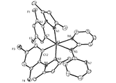
- FIG. 14 is a diagram showing a single crystal structure of still another complex compound according to the present invention.
- FIG. 15 is a graph showing the PL spectrum of the complex compound shown in FIG. 14 observed in degassed dichloromethane.
- FIG. 16 is a graph showing the UV-Vis absorption spectrum and PL spectrum of still another complex compound according to the present invention observed in degassed dichloromethane.
- FIG. 17 is a diagram showing a single crystal structure of the complex compound observed in FIG.
- the novel complex compound according to the present invention has a structure represented by the following general formula (1).
- C ⁇ N represents a cyclometalated ligand.
- A1 location indicated by A1; hereinafter referred to as “A1”
- the plurality of A1 may represent the same cyclometalated ligand, May be represented.
- the plurality of A1 are preferably the same cyclometalated ligand.
- the part of a cyclometalated ligand functions as a part (luminescent ligand) which is directly related to the light emission phenomenon exclusively in the novel complex compound according to the present invention. That is, it functions as a portion where light emission from the excited triplet (phosphorescence emission) occurs.
- N ⁇ N (location indicated by A2; hereinafter referred to as “A2”) is presumed to function as an auxiliary ligand involved in the stereocontrol of the novel complex compound according to the present invention. . And it is estimated that it has a potential hole transport ability by the lone electron pair which N has.
- A2 location indicated by A2; hereinafter referred to as “A2”
- the plurality of A2 may be the same or different from each other.
- A2 is specifically an auxiliary ligand represented by the following general formula (2) or the following general formula (3).
- * indicates coordination to M.
- R1 to R8 are each independently a hydrogen atom; a halogen atom; a silyl group; an alkylsilyl group; or a hydrocarbon group having 1 to 10 carbon atoms; To express.
- the hydrocarbon group preferably contains 1 to 5 carbon atoms.
- at least one hydrogen atom contained in the hydrocarbon group may be substituted with a halogen atom such as fluorine, chlorine, bromine and iodine.
- a part of the carbon atoms may be substituted with at least one of a sulfur atom and an oxygen atom.
- hydrocarbon groups are connected to each other to form an aromatic ring
- R1 and R5 are the same, R2 and R6 are the same, R3 and R7 are the same, and R4 and R8 are the same It is preferable that
- auxiliary ligand represented by the general formula (2) include the auxiliary ligands represented by the following chemical formulas (7) to (12), but are not limited thereto. Absent. In each formula, * indicates coordination to M.
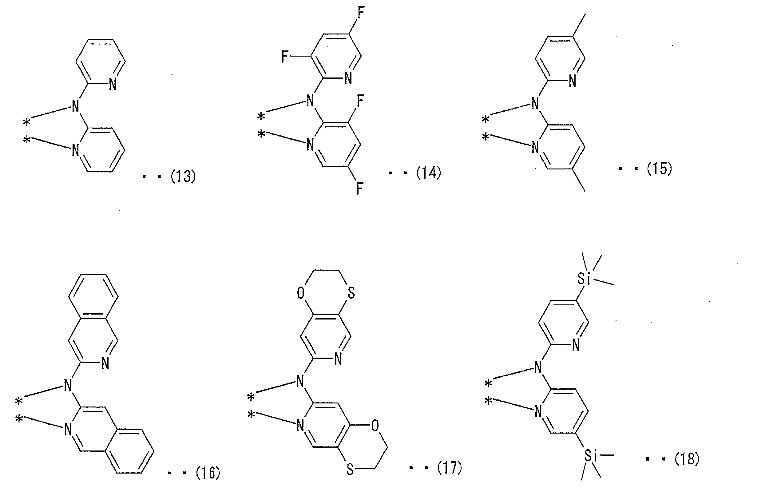
- auxiliary ligand represented by the general formula (3) include, but are not limited to, the auxiliary ligands represented by the following chemical formulas (13) to (18). It is not a thing. In each formula, * indicates coordination to M.
- cyclometalated ligand any ligand known to be directly involved in the light emission phenomenon of the metal complex can be adopted, and desired light emission characteristics (emission wavelength, etc.) can be adopted. What is necessary is just to select suitably according to. Specific examples include, but are not limited to, cyclometalated ligands represented by (a) to (q) of the following chemical formula (19).
- the hydrogen atom on the aromatic ring, the heterocyclic ring, or other carbon is, for example, a halogen group such as a fluorine atom, a chlorine atom, a bromine atom, and an iodine atom;
- a hydrocarbon group such as an alkyl group having 1 to 6 alkyl groups
- a halogenated hydrocarbon group such as a halogenated alkyl group having 1 to 20 carbon atoms, preferably 1 to 6 carbon atoms
- an amino group an alkoxy group
- It may be substituted by a substituent such as an alkoxy group; an aromatic ring, a heterocyclic ring, or a saturated or unsaturated hydrocarbon ring
- the cyclometalated ligand represented by the chemical formula (19) is a structure further provided with a cyclic structure such as one to several aromatic rings, heterocyclic rings, or saturated or unsaturated hydrocarbon rings. Also good.
- cyclometalated ligand A1 is preferably represented by the following general formula (4), the following general formula (5), or the following general formula (6).
- R11 to R18 each independently represent a hydrogen atom; a halogen atom; or a hydrocarbon group having 1 to 10 carbon atoms.
- the hydrocarbon group preferably contains 1 to 5 carbon atoms.
- at least one hydrogen atom contained in the hydrocarbon group may be substituted with a halogen atom such as fluorine, chlorine, bromine and iodine.
- a halogen atom such as fluorine, chlorine, bromine and iodine.
- some of the said carbon atoms may be substituted by the sulfur atom or the nitrogen atom.
- hydrocarbon groups are connected to each other to remove an aromatic ring, a saturated or unsaturated hydrocarbon ring (excluding the aromatic ring) Or a heterocycle containing a sulfur atom and / or a nitrogen atom (heteroatom).
- * indicates coordination to M.
- X represents an oxygen atom or a sulfur atom
- R19 to R26 each independently represent a hydrogen atom; a halogen atom; or a hydrocarbon group having 1 to 10 carbon atoms.
- the hydrocarbon group preferably contains 1 to 5 carbon atoms.
- at least one hydrogen atom contained in the hydrocarbon group may be substituted with a halogen atom such as fluorine, chlorine, bromine and iodine.
- the said hydrocarbon group contains two or more carbon atoms, some of the said carbon atoms may be substituted by the sulfur atom or the nitrogen atom.
- hydrocarbon groups are connected to each other to form an aromatic ring, a saturated or unsaturated hydrocarbon ring (excluding an aromatic ring), or a sulfur atom and A heterocycle containing a nitrogen atom (heteroatom) may be constituted.
- * indicates coordination to M.
- R27 to R33 each independently represent a hydrogen atom; a halogen atom; or a hydrocarbon group having 1 to 10 carbon atoms.
- the hydrocarbon group preferably contains 1 to 5 carbon atoms.
- at least one hydrogen atom contained in the hydrocarbon group may be substituted with a halogen atom such as fluorine, chlorine, bromine or iodine.
- a halogen atom such as fluorine, chlorine, bromine or iodine.
- some of the said carbon atoms may be substituted by the sulfur atom or the nitrogen atom.
- hydrocarbon groups are connected to each other to form an aromatic ring, a saturated or unsaturated hydrocarbon ring (excluding an aromatic ring), or a sulfur atom and A heterocycle containing a nitrogen atom (heteroatom) may be constituted.
- * indicates coordination to M.
- the central metal M is a metal arbitrarily selected from transition metal atoms.
- iridium (Ir) platinum, palladium, rhodium, rhenium, ruthenium, osmium, thallium, lead , Bismuth, indium, tin, antimony, tellurium, gold, silver, and the like, among which iridium, osmium, and platinum are more preferable, and iridium is particularly preferable.
- n and n are both integers of 1 or more, and the sum of m and n is preferably not more than the maximum number of ligands that can coordinate to the central metal M, preferably Is the same as the maximum number.
- n is 1 and m is (the maximum number of ligands that can be coordinated to the central metal M-1) in order to obtain better light emission characteristics. It is more preferable.
- the central metal M is iridium
- the sum of m and n is 3 or less, so that n is 1 and m is preferably 2.
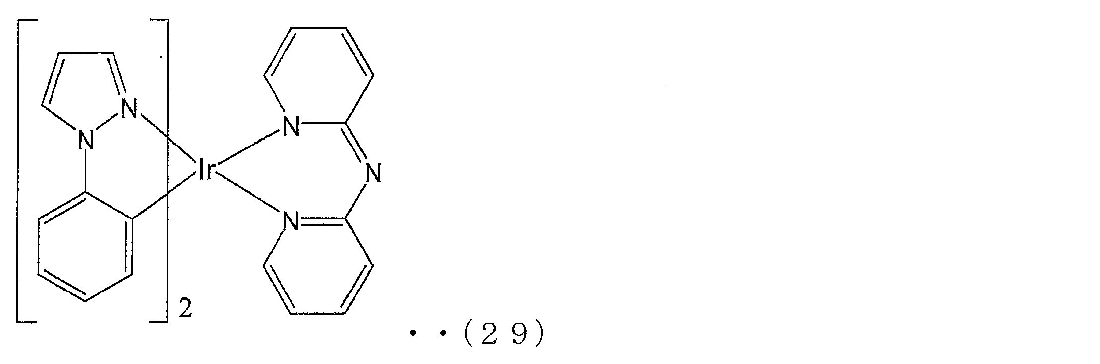
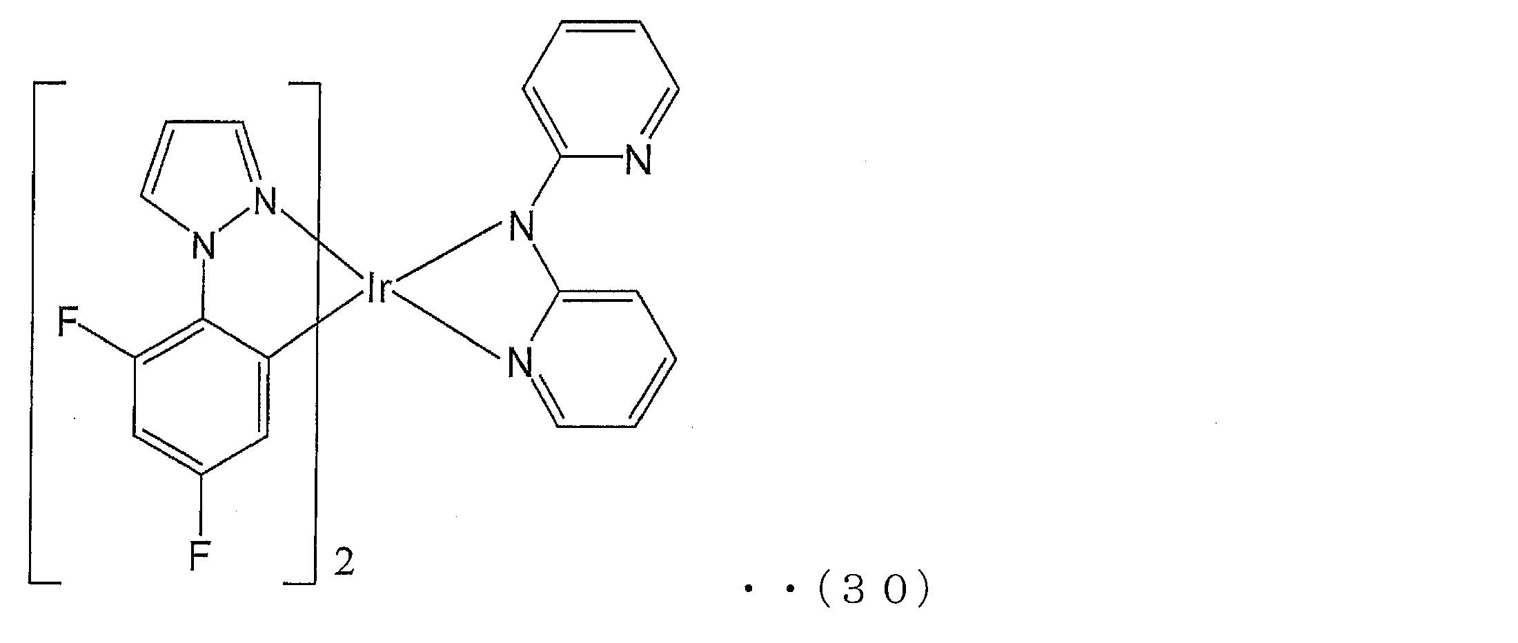
- Such a novel complex compound is not particularly limited, but specific examples include complex compounds described in the following chemical formulas (28) to (31).
- the new complex compound bis (2-phenylpyridine) iridium (III) (dipyridylamide) represented by the chemical formula (28) is referred to as Ir (ppy) 2- (dpa)
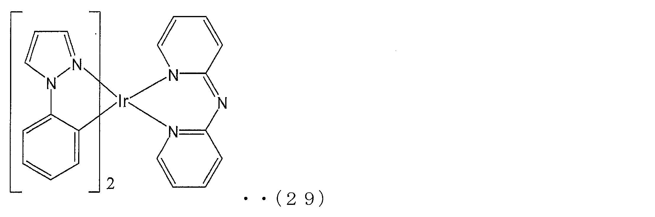
- the new complex compound bis ( Phenylpyrazole) iridium (III) (dipyridylamide) is referred to as Ir (ppz) 2- (dpa)
- Dipyridylamide) is called Ir (dfppz) 2- (dpa) and is a new complex compound bis (2,4- (difluorophenyl) -3,5-dimethylpyrazole) iridium (III) (dipyridylamide) represented by chemical formula (31) ) Is
- Ir (ppy) 2- (dpa), Ir (ppz) 2- (dpa), Ir (dfppz) 2- (dpa) and Ir (dfmppz) 2- (dpa) are in turn as cyclometalated ligands, 2-phenylpyridine, phenylpyrazole, 2,4- (difluorophenyl) pyrazole and 2,4- (difluorophenyl) -3,5-dimethylpyrazole are used.
- any new complex compound uses dipyridylamide as an auxiliary ligand.
- the complex compound according to the present invention comprises the step (1) of obtaining the primary metal complex by coordinating the cyclometalated ligand to the central metal M, and then the auxiliary ligand as the primary metal complex. And a step (2) of obtaining a complex compound according to the present invention by coordination.
- This method is a simple reaction of two-step coordination formation, and has an advantage that a compound having excellent emission characteristics can be easily synthesized because an auxiliary ligand having a simple chemical structure is used.
- the time and conditions are such that the halide (metal chloride, etc.) of the central metal M and the cyclometalated ligand are sufficiently coordinated. It can be carried out with reference to known methods described in, for example, M.MNonoyama, Bull. Chem. Soc. Jpn. 1974, 47, 767.
- an excess amount of the cyclometalated ligand may be allowed to coexist with one mole equivalent of the halide of the central metal M. More specifically, m in the general formula (1) A corresponding equivalent amount or more of cyclometalated ligands may be present together.
- the central metal M is iridium
- 2 mole equivalents or more, more preferably 2.5 to 3 mole equivalents of a cyclometalated ligand can coexist with 1 mole equivalent of an iridium halide. That's fine.
- Step (1) can be performed in a solvent that is not reactive with the halide of the central metal M and the cyclometalated ligand.
- a solvent that is not reactive with the halide of the central metal M and the cyclometalated ligand.
- examples of such a solvent include 2-methoxyethanol, tetrahydrofuran (THF). ), Ethoxyethanol, and the like.
- THF tetrahydrofuran
- Ethoxyethanol ethoxyethanol
- what mixed these solvents and water can also be used as a solvent as needed.
- the reaction temperature and reaction pressure in step (1) may be room temperature and normal pressure, but when the solvent is refluxed, for example, the reaction may be performed at a temperature and pressure at which the solvent can be evaporated.
- the primary metal complex and the auxiliary ligand obtained in the step (1) may be allowed to coexist for a time and under a condition that both are sufficiently coordinated.
- the complex compound represented by the formula (30) it is preferable to react at room temperature because the compound can be produced with high selectivity.
- the auxiliary ligand can be obtained by extracting a proton from a compound represented by the following general formula (20) and anionizing it.
- a compound represented by the following general formula (20) and n-BuLi and lithiating (amidating) the compound represented by the following general formula (20) an auxiliary ligand can be obtained.
- the base for extracting protons is not limited to n-BuLi, and for example, alkali metal hydrides such as NaH and KH can be used.
- R1 to R8 in the general formula (20) are the same as those described in the general formulas (2) and (3).
- Specific examples of the compound represented by the general formula (20) include compounds represented by the following chemical formulas (21) to (26), but are not limited thereto.
- an excess amount of auxiliary ligand may be allowed to coexist with 1 mole equivalent of the halide of the central metal M, and more specifically, it corresponds to n in the general formula (1). What is necessary is just to coexist an auxiliary ligand more than an equivalent.
- an auxiliary ligand of 1 molar equivalent or more, more preferably 1.5 to 2 molar equivalents may coexist with 1 molar equivalent of the iridium.
- Step (2) can be performed in a solvent that is not reactive with the halide of the central metal M and the auxiliary ligand.
- a solvent examples include 2-methoxyethanol, tetrahydrofuran, and ethoxyethanol. Etc.
- what mixed these solvents and water can also be used as a solvent as needed.
- the reaction temperature and reaction pressure in step (2) may be room temperature or normal pressure, but when the solvent is refluxed, for example, the reaction may be performed at a temperature and pressure at which the solvent can be evaporated.
- the step (2) is preferably performed in an atmosphere of an inert gas such as argon.
- a step of purifying the reaction product and other steps can be included as appropriate.
- novel complex compound according to the present invention can be vacuum-deposited, an example of its use is a light-emitting material of organic light-emitting devices (OLEDs: Organic Light-Emitting Devices). Moreover, the use as a detection marker using the property to light-emit is also considered.
- the novel complex compound is, for example, 1) a point that N in the auxiliary ligand has a potential hole transport ability due to the lone pair of electrons, and 2) a new complex by steric control by the auxiliary ligand. It has advantageous features as a luminescent material, such as the interaction between luminescent sites (cyclometalated ligands) within a compound or between new complex compounds being considered to be reduced.
- the phosphor emits practically sufficient phosphorescence even at room temperature by applying a voltage, and 2) the phosphorescence emission life is extremely short, and self-quenching is suppressed to the minimum. 3) Emits light when a relatively low voltage is applied (light emission efficiency is good), 4) It exhibits characteristics such as light emission efficiency that hardly deteriorates even under a relatively high density current, and excellent durability. It is particularly suitable as a luminescent material by application. More specifically, it is particularly suitable as a light-emitting material such as an organic electroluminescence (EL) element, a detection marker for detecting an object based on the presence or absence of light emission by voltage application, and the like.
- EL organic electroluminescence
- An organic EL display panel (an example of an organic EL element) has characteristics that it is suitable for moving image reproduction with a high-speed response and can be made thinner than a liquid crystal display panel.
- deterioration of the light emitting material due to voltage application, light emission efficiency, and the like are major issues.
- each pixel becomes small, and thus there is a problem that it is necessary to apply a higher voltage to the light emitting material in order to ensure practically sufficient luminance.
- novel complex compound according to the present invention is used as a light emitting material, for example, it is possible to provide an organic EL display panel having a long product life, excellent luminous efficiency, low power consumption, and high definition (for example, VGA or more). It becomes.
- the present invention further includes a light emitting element (organic EL element) comprising a pair of electrodes and a light emitting layer containing a light emitting material disposed between the electrodes, wherein the light emitting layer includes the compound according to the present invention.
- a light emitting element organic EL element
- the organic EL element will be specifically described.
- the electrode in the organic EL element includes at least a positive electrode and a negative electrode.
- the positive electrode is not particularly limited, but a transparent electrode such as ITO (Indium-Tin Oxide) is usually used to extract light from the light emitting layer to the outside.
- ITO Indium-Tin Oxide
- the negative electrode is not particularly limited, for example, an aluminum electrode can be used.
- the thickness of the said positive electrode and negative electrode is not specifically limited, For example, it is 50 nm or more and 400 nm or less, Preferably it exists in the range of 100 nm or more and 300 nm or less.
- the resistance value of the positive electrode and the negative electrode is, for example, in the range of 5 ⁇ to 50 ⁇ , preferably 10 ⁇ to 30 ⁇ .
- the light emitting layer comprises a compound according to the present invention as a light emitting material.
- the light emitting layer can be formed by a known method for forming a thin film, such as a vapor deposition method and a cast film method, and the vapor deposition method is particularly preferable.
- the thickness of a light emitting layer is not specifically limited, For example, it is 20 nm or more and 40 nm or less, Preferably it exists in the range of 30 nm or more and 40 nm or less.
- the light emitting layer may contain only the compound according to the present invention as a light emitting material, or may further contain another compound as a light emitting material.
- the light emitting dopant may be used as the compound according to the present invention, and the light emitting host may be doped.
- the content ratio of the luminescent dopant and the luminescent host may be appropriately set according to desired luminescent characteristics.
- the proportion of the luminescent dopant in the luminescent material is preferably in the range of 3% by weight to 80% by weight, more preferably in the range of 5% by weight to 40% by weight. More preferably, it is in the range of not less than 20% by weight.
- a known host such as 4,4'-N, N'-dicarbazole-biphenyl (CBP) may be appropriately used as the light emitting host.
- the emission characteristics can be appropriately changed according to the type of the emission host or the doping amount.
- OLEDs of a type in which a light emitting host is doped with a light emitting dopant are referred to as doped OLEDs, and OLEDs made of only one kind of light emitting material (not having a doped structure) are referred to as undoped OLEDs.
- light emission characteristics can be changed suitably by changing the kind of cyclometalation ligand contained in the compound of this invention.
- the organic EL device has a hole injection layer, a hole transport layer, a hole blocking layer, an electron transport layer made of a known material as necessary in order to promote recombination of holes and electrons in the light emitting layer.
- An electron injection layer or the like may be further included.
- Example 1 Synthesis of Ir (ppy) 2- (dpa) and analysis of its structure] (Synthesis of cyclometallated Ir (III) ⁇ -chloride crosslinking precursor)
- the cyclometalated Ir (III) ⁇ -chloride bridged dimer (primary metal complex) represented by the general formula C ⁇ N 2 Ir ( ⁇ -Cl) 2 IrC ⁇ N 2 is prepared by the method of M. Nonoyama et al. Nonoyama, Bull. Chem. Soc. Jpn. 1974, 47, 767) was synthesized according to an improved method.
- reaction product was filtered through a Buchner funnel. Subsequently, the residue obtained by filtration was washed several times with hexane and ethyl ether to obtain a crude product.
- the yield of ⁇ -chloride bridged dimer ([Ir (ppy) 2 ( ⁇ -Cl)] 2 ) containing phenylpyridine ligand was 80%.
- the obtained ⁇ -chloride cross-linked dimer was analyzed by NMR and confirmed to be the target product. The results of the analysis are shown below.
- FIG. 1 shows an outline of a single crystal structure of Ir (ppy) 2- (dpa).
- B) in FIG. 1 shows an outline of crystal packing of Ir (ppy) 2- (dpa).
- B) in FIG. 1 shows the crystal packing of the closest molecule in which the pyridyl ring (ppy) is on the phenyl ring of the adjacent molecule and has a C2 rotation relationship.
- the distance between the planes of adjacent phenyl rings is about 3.3 mm.
- Example 2 Absorption, photoluminescence (PL), and electrochemical measurement in Ir (ppy) 2- (dpa)]
- Absorption spectrum and PL spectrum The absorption spectrum was obtained using a UV-2550 UV-vis spectrometer (trade name, manufactured by Shimadzu Corporation).
- the PL spectrum was recorded using an RF5301PC fluorescence spectrometer (trade name, manufactured by Shimadzu Corporation) equipped with a xenon arc lamp as an excitation source.
- a solution prepared by dissolving iridium complex in spectral analysis grade CHCl 3 was used.
- error bars of ⁇ 10% were obtained.
- Luminescent lifetime was measured using a streak camera base system C4780 (trade name of Hamamatsu) combined with a femtosecond Ti: sapphire laser system (Spectra-Physics, Spitfire).
- the excitation wavelength was 397 nm
- the detection wavelength was 450 to 700 nm.
- the time resolution was 30-40 ns.
- an error bar of ⁇ 10% was obtained.
- Electrochemical measurement was performed using a cyclic voltammetry HSV-100 (manufactured by Hokuto Denko) and an electrochemical work station. More specifically, a platinum rod is used as the working electrode, a platinum wire is used as the auxiliary electrode, an Ag / AgNO 3 electrode is used as the reference electrode, and standardized for the ferrocene / ferrocenium pair.
- the cyclic voltammetry was performed at a scan rate of 100 mV / s. Each measurement was calibrated with an internal standard, a ferrocene / ferrocenium (Fc) redox system.
- the electrochemical behavior of Ir (ppy) 2- (dpa) was examined by cyclic voltammetry using ferrocene as an internal standard. The measurement was performed in an acetonitrile solvent containing 0.1 M TBAP.
- Thermal stability was measured using a thermogravimetric measuring apparatus TGA-50 (manufactured by Shimadzu Corporation). More specifically, a sample of 2 mg was placed on an aluminum pan, and the temperature was raised to 450 ° C. at a rate of 10 ° C./min.
- FIG. 2 shows the UV-Vis absorption spectrum and PL spectrum of the novel iridium complex observed in degassed dichloromethane or in the solid phase.
- the strong absorption at 250-350 nm involves the IL ⁇ - ⁇ * transition where spin is allowed on the cyclometalated ligand (IL).
- the relatively weak absorption at 350-400 nm is due to the spin allowed for the metal-ligand charge transfer (MLCT) transition.
- MLCT metal-ligand charge transfer
- the absorption at 400 to 470 nm is considered to involve MLCT and ⁇ - ⁇ * transition.
- the iridium complex Ir (ppy) 2- (dpa) exhibited a bluish green emission in dichloromethane.
- the emission showed a maximum at a wavelength of 480 nm and a shoulder peak at a wavelength of 510 nm.
- the PL spectrum of the iridium complex thin film (corresponding to the solid phase state) showed a deep color shift with a maximum value of 530 nm, and emitted light in a wider range.
- Luminescence lifetime is one of the important factors in triplet-triplet decay. It is known that the longer the phosphorescent emission lifetime, the potentially more triplet-triplet decay of the material.
- FIG. 3 shows the phosphorescence emission delay time in THF solution. The emission lifetime of phosphorescence of Ir (ppy) 2- (dpa) was 0.17 ⁇ s when excitation light having a wavelength of 402 nm was given at ambient temperature in a THF solution.
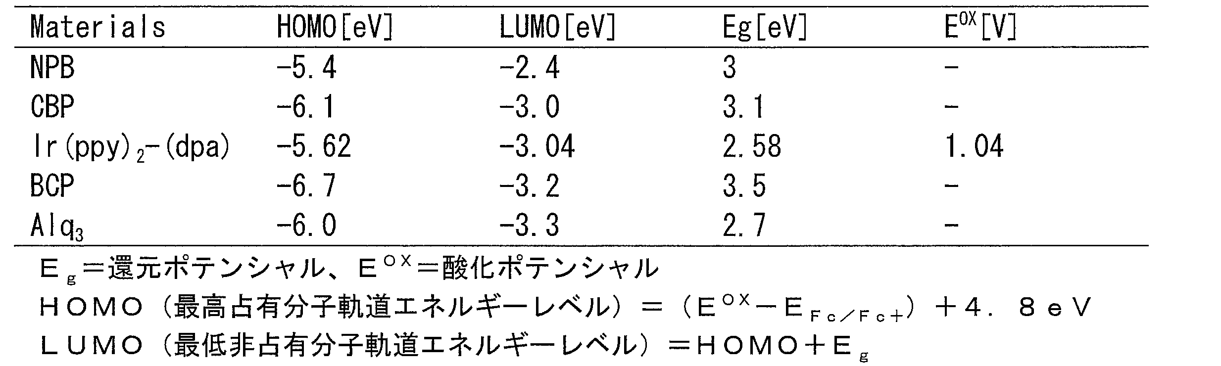
- Electrochemical measurement Table 1 shows the results of the electrochemical measurement.
- the reduction potential was estimated from the onset wavelength showing the optimum absorption.
- literature values are described for materials NPB, CBP, BCP, and AlQ (Alq 3 ) used in Example 3 described later.
- the oxidation potential of Ir (ppy) 2- (dpa) was 1.04V.
- FIG. 4 shows a cyclic voltammograph in acetonitrile.
- TGA thermogravimetric analysis
- Example 3 Production of OLEDs using Ir (ppy) 2- (dpa), measurement of electroluminescence (EL)]
- undoped OLEDs here, diodes
- a glass substrate sheet resistance: 20 ⁇ / cm 2
- ITO to become an anode
- an oxygen plasma treatment was applied to the ITO surface for 15 minutes.
- N, N′-diphenyl-N, N′-bis (1-naphthyl) -1,1′-diphenyl-4,4′-diamine NB
- an iridium complex which is an organic material
- BCP 2,9-dimethyl-4,7-diphenyl-1,10-phenanthroline
- Alq 3 8-hydroxyquinoline aluminum
- All the organic materials were purified by a continuous sublimation method and thermally deposited at a rate of 1.0 kg / s under a pressure of 8 ⁇ 10 4 Pa.
- the film thicknesses of NPB, iridium complex, BCP, and AlQ are 30 nm, 25 nm, 6 nm, and 20 nm, respectively.
- the thickness of the deposited layer was measured in situ with a quartz crystal monitor.
- LiF lithium fluoride
- the active area of the electrode part was 5 ⁇ 5 mm 2 .
- the NPB layer is a hole transport layer
- the iridium complex layer is a light emitting layer
- the BCP layer is a hole blocking layer
- the AlQ layer is an electron transport layer
- the LiF layer is an electron injection layer
- the aluminum layer is a metal cathode. Functions as a layer.
- the chemical structure of these materials and the structure of OLEDs are shown in FIG.
- doped OLEDs I to III were manufactured by using the iridium complex according to the present invention as a light emitting dopant and doping CBP as a light emitting host.
- the thicknesses of the light emitting layers of the doped OLEDs I to III are all 25 nm, and sequentially contain iridium complexes as light emitting dopants at concentrations of 5 wt%, 10 wt%, and 20 wt%.
- the configuration and manufacturing method other than the composition of the light emitting layer are the same as those of the undoped OLEDsIV.
- EL electroluminescence
- I-IV The EL spectra of the prepared OLEDs I to IV were measured at room temperature using a high resolution spectrometer (Stellar net Blue wave UV-VIS-NIR).
- the current density-voltage-luminance (IVL) characteristics of the fabricated OLEDs I-IV are as follows. At room temperature, luminance meter Chroma-Meter CS-200 (manufactured by Konica Minolta) and Keithley 2400 program controlled voltage current digital source meter (Keithley 2400 programmable) voltage-current digital source meter). The results are shown in FIGS.
- FIG. 6 is a diagram showing the results of measuring the EL intensity at each wavelength
- FIG. 7 is a diagram showing the results of measuring the EL intensity by changing the drive voltage in OLEDsI. All OLEDs I to IV emitted green light at a driving voltage of 9V. The OLEDsI emitted green light regardless of the applied drive voltage (6V to 12V). Further, in any OLEDs, even when the driving voltage was high, another light emission did not occur from the host layer or the adjacent layer. This indicates a complete transfer of energy and / or charge from the host exciton to the phosphor. In each OLED, there was no significant change in the EL spectrum and CIE chromaticity coordinates when the current and bias voltage were changed.
- the maximum of the EL spectrum of doped OLEDs was slightly red-shifted from 513 nm to 530 nm as the dopant concentration increased. This is considered to be because stronger intermolecular interactions occur as the dopant concentration is higher, as seen in the PL spectrum.
- FIG. 8 shows measurement results of luminance-voltage characteristics and current density-voltage characteristics of OLEDs I to IV. Compared to undoped OLEDs IV, the driving voltages of doped OLEDs I-III were lower. In the OLEDsI having the lowest doping concentration, the driving voltage was the lowest. Although there was no difference in current density-voltage characteristics in OLEDs II to IV, OLEDsI having the lowest doping concentration was superior in current density-voltage characteristics compared to other OLEDs.
- FIG. 9 shows measurement results of current efficiency-current density characteristics and energy efficiency-current density characteristics of OLEDs I to IV.
- doped OLEDs I to III were superior in current efficiency and energy efficiency.
- the current efficiency and the energy efficiency at a current density of 2 mA / cm 2 were 120 cd / A and 43 lm / W, respectively, and were highest in the OLEDs I to IV.
- These values in OLEDs I to IV are based on the green light-emitting devices reported so far in which Ir (III) is doped into CBP (see the following document: Baldo MA et al, Appl. Phys. Lett., 1999, 75).
- OLEDsI also showed excellent current efficiency (39 cd / A) and energy efficiency (6.8 lm / W) even at a high current density (94 mA / cm 2 ).
- Table 2 summarizes the characteristics of each OLED.
- FIG. 10 is a diagram showing the result of measuring the EL intensity by changing the drive voltage. As shown in FIG. 10, OLEDsV also emitted green light regardless of the applied drive voltage.
- FIG. 11 shows measurement results of luminance-voltage characteristics and current density-voltage characteristics. Compared with OLEDs I to IV (see FIG. 8), the luminance and current of OLEDsV were lower.
- FIG. 12 shows measurement results of current efficiency-current density characteristics and energy efficiency-current density characteristics of OLEDsV. The current efficiency-current density characteristics and energy efficiency-current density characteristics of OLEDsV were low compared to the current efficiency-current density characteristics and energy efficiency-current density characteristics of OLEDs I to IV (see FIG. 9).
- Example 4 Synthesis of Ir (ppz) 2- (dpa) and analysis of its structure] (Synthesis of cyclometallated Ir (III) ⁇ -chloride crosslinking precursor) Cyclometalated Ir (III) ⁇ -chloride bridged dimer (primary metal complex) in the same manner as in Example 1 except that 0.211 g of phenylpyrazole was used as the cyclometalated ligand used in the reaction. ) was synthesized. The yield of the ⁇ -chloride bridged dimer ([Ir (ppz) 2 ( ⁇ -Cl)] 2 ) containing the phenylpyrazole ligand was 85%. The obtained ⁇ -chloride cross-linked dimer was analyzed by NMR and confirmed to be the target product.
- Example 5 Measurement of PL spectrum in Ir (ppz) 2- (dpa)
- the PL spectrum of Ir (ppz) 2- (dpa) was measured.
- the measurement results are shown in FIG. FIG. 13 shows the PL spectrum of Ir (ppz) 2- (dpa) observed in degassed dichloromethane.
- Ir (ppz) 2- (dpa) exhibited a PL maximum at a wavelength of 492 nm.
- Example 7 Measurement of PL spectrum in Ir (dfppz) 2- (dpa)
- the PL spectrum of Ir (dfppz) 2- (dpa) was measured.
- the measurement results are shown in FIG.
- FIG. 15 shows the PL spectrum of Ir (dfppz) 2- (dpa) observed in degassed dichloromethane.
- Ir (dfppz) 2- (dpa) showed a PL maximum at a wavelength of 500 nm.
- Example 8 Synthesis of Ir (dfmppz) 2- (dpa) and analysis of its structure
- Synthesis of cyclometalated ligand The cyclometalated ligand 2,4- (difluorophenyl) -3,5-dimethylpyrazole (dfmppz) was prepared according to the method of Yang et al. (Non-patent document: C.-H. Yang et al, Inorg. Chem. , 2005, 44, 7770-7780.).
- Example 9 Measurement of absorption spectrum and PL spectrum in Ir (dfmppz) 2- (dpa)
- the UV-Vis absorption spectrum and PL spectrum of Ir (dfmppz) 2- (dpa) were measured.
- the measurement results are shown in FIG. FIG. 16 shows the UV-Vis absorption spectrum and PL spectrum of Ir (dfmppz) 2- (dpa) observed in degassed dichloromethane.
- Ir (dfmppz) 2- (dpa) showed a PL maximum at a wavelength of 505 nm and a shoulder peak at 450 nm.
- the present invention it is possible to provide a novel complex compound exhibiting practically sufficient light emission characteristics, a light emitting method using the compound, and a light emitting element even when used alone, as well as a light emitting dopant.
- the present invention can be suitably used as, for example, a detection marker or a light emitting material of an organic electroluminescence element.
Landscapes
- Chemical & Material Sciences (AREA)
- Organic Chemistry (AREA)
- Engineering & Computer Science (AREA)
- Materials Engineering (AREA)
- Crystallography & Structural Chemistry (AREA)
- Inorganic Chemistry (AREA)
- Electroluminescent Light Sources (AREA)
Abstract
熱安定性、及び発光特性に優れた新規錯体化合物を提供するため、本発明に係る錯体化合物は、一般式(1)で示されるものである。
Description
本発明は、新規錯体化合物、及び当該錯体化合物の利用に関するものである。より詳細には、当該錯体化合物を含む発光素子に関するものである。
りん光発光する金属錯体を発光材料とした有機発光素子(以下「OLEDs」と称する:Organic Light-Emitting Devices)は、蛍光発光材料より発光効率が著しく高いため注目を集めている。
上記発光材料となる、白金、オスミウム又はイリジウムを含む重金属錯体のなかで、イリジウム錯体は最も発光効率が高い。これまでに、種々の配位子を有するイリジウム錯体が開発されてきている(特許文献1、非特許文献1~4)。
C. K. George and W. R. McWhinnie, J. Chem. Soc., 1965, p7145.
L. H. Wen, P. S. Donald and M. K. DeArmond, J. Phys. Chem., 1981, 85, p2080.
R. L. Jen, R. L. Yeong and L. H. Wen, Inorg. Chim. Acta, 2001, 319, p83.
C. T. Mei, L. S. Wei, C. Y. Yu, P. W. Shao and L. H. Wen, Inorg. Chim. Acta, 2006, 359, p4144.
上記特許文献1に開示されたイリジウム錯体は実用上充分な発光特性を示すものの、いまだ改善の余地がある。
上記非特許文献1~4に開示されたイリジウム錯体はジピリジルアミン(DpaH)配位子を有するものである。有機エレクトロルミネセンス(EL)素子を作製するために、発光材料を真空蒸着させるためには、発光材料を昇華させる必要がある。しかしながら、上記非特許文献1~4に開示されたイリジウム錯体はいずれもイオン性の錯体であり、昇華させようとしても、昇華の前に錯体が分解してしまうという問題がある。すなわち、これらイリジウム錯体の昇華が不可能であり、これらイリジウム錯体を用いての真空蒸着によるEL素子の作製は不可能であった。したがって、これらイリジウム錯体をEL材料として利用することはできなかった。
そこで、本発明は上記の問題点に鑑みてなされたものであり、その目的は、真空蒸着が可能であり、発光特性に優れた新規錯体化合物を提供することにある。
本願発明者らは上記課題を解決するために鋭意検討をおこなった。その結果、特定の構造を有する補助配位子を使用することで、優れたりん光発光特性を示し、中性で熱安定性に優れた錯体化合物が得られることを見出し、本願発明を完成させるに至った。
すなわち、本発明に係る錯体化合物は、上記課題を解決するために、下記の一般式(1)で表される錯体化合物であることを特徴としている。これによれば、中性の錯体で熱安定性に優れているため真空蒸着が可能であり、エネルギー効率等の発光特性に優れた新規錯体化合物を提供することができるという効果を奏する。
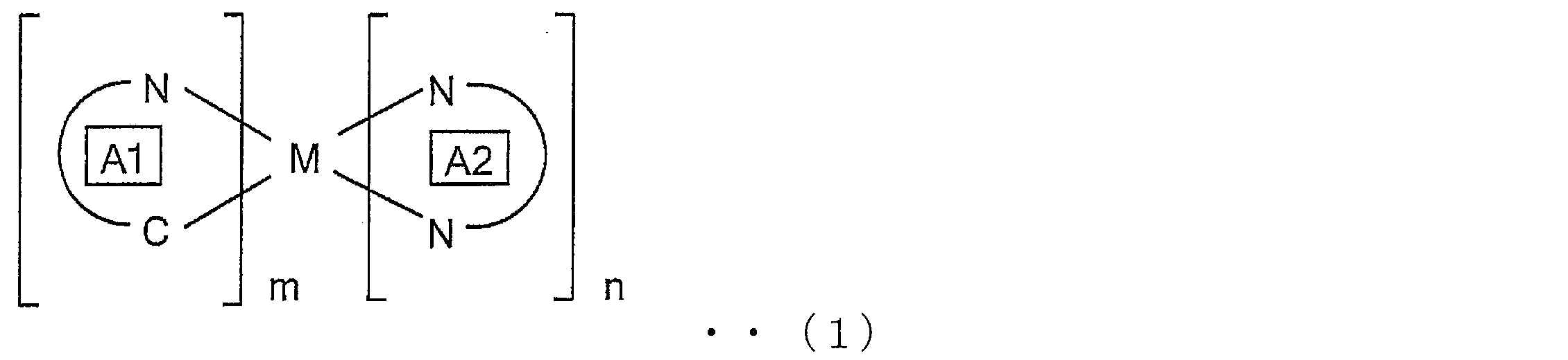
(一般式(1)中、C^N(A1で示す箇所)はシクロメタル化配位子を表し、N^N(A2で示す箇所)は下記一般式(2)又は下記一般式(3)で表される補助配位子を表し、Mは遷移金属原子を表す。
mおよびnはいずれも1以上の整数であり、mとnとの合計は、Mに配位することができる配位子の最大数以下である。)
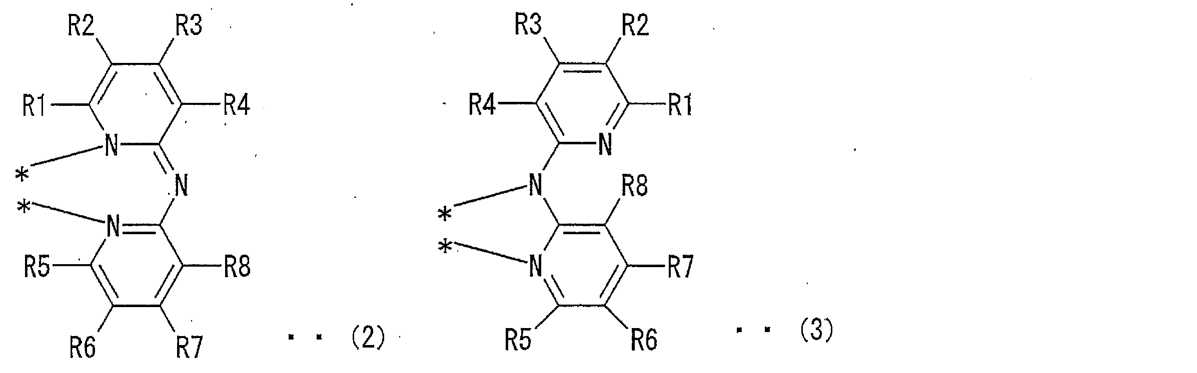
(一般式(2)及び(3)中、R1~R8は互いに独立して、水素原子;ハロゲン原子;シリル基;アルキルシリル基;又は炭素数1~10個の炭化水素基;を表し、炭化水素基に含まれる少なくとも一つの水素はハロゲン原子で置換されていてもよく、炭化水素基が2個以上の炭素原子を含む場合に当該炭素原子の一部が硫黄原子又は酸素原子で置換されていてもよく、炭化水素基同士が互いに連結して環を形成してもよい。一般式(2)及び(3)中、*はMへの配位を示す。)
本発明に係る発光方法は、上記の錯体化合物に電圧を印加して、当該錯体化合物を発光させることを特徴としている。
本発明に係る発光方法は、上記の錯体化合物に電圧を印加して、当該錯体化合物を発光させることを特徴としている。
本発明に係る発光素子は、一対の電極と、該一対の電極間に配された発光材料を含む発光層とを含んでなる発光素子であって、上記発光層が上記の錯体化合物を含んでなることを特徴としている。これによれば、実用上充分な発光特性を示す発光素子を提供することができる。
本発明に係る錯体化合物及びその利用によれば、中性の錯体で熱安定性に優れているため真空蒸着が可能となり、エネルギー効率等の発光特性に優れた新規錯体化合物、当該錯体化合物を用いた発光方法、及び発光素子を提供することができるという効果を奏する。
本発明に係る新規錯体化合物は、以下の一般式(1)に示す構造を有するものである。

ここで、上記一般式(1)中、C^N(A1で示す箇所。以下「A1」という。)はシクロメタル化配位子を表す。なお、A1が複数ある場合(後述するmが2以上の整数の場合)には、複数のA1は、同一のシクロメタル化配位子を表してもよく、互いに異なるシクロメタル化配位子を表してもよい。新規錯体化合物の合成の容易さ、及び当該錯体化合物の発光特性を増強する観点からは、複数のA1は、同一のシクロメタル化配位子であることが好ましい。なお、シクロメタル化配位子の部分は、本発明に係る新規錯体化合物において専ら発光現象に直接関わる部分(発光性の配位子)として機能する。すなわち、励起3重項からの発光(りん光発光)が生じる部分として機能する。
上記一般式(1)中、N^N(A2で示す箇所。以下「A2」という。)は本発明に係る新規錯体化合物の立体制御に関わる補助配位子として機能していると推定される。そして、Nが有する孤立電子対により、潜在的な正孔輸送能も持つと推定される。なお、A2が複数ある場合(後述するnが2以上の整数の場合)には、複数のA2は同一であってもよく、互いに異なっていてもよい。
A2は、具体的には、下記一般式(2)又は下記一般式(3)で表される補助配位子である。なお、式中、*はMへの配位を示している。

上記一般式(2)及び上記一般式(3)中、R1~R8は互いに独立して、水素原子;ハロゲン原子;シリル基;アルキルシリル基;又は炭素数1~10個の炭化水素基;を表す。ここで、当該炭化水素基に含まれる炭素数は好ましくは1~5個である。また、当該炭化水素基に含まれる少なくとも一つの水素原子は、フッ素、塩素、臭素及びヨウ素等のハロゲン原子で置換されていてもよい。また、当該炭化水素基が2個以上の炭素原子を含む場合に、当該炭素原子の一部が硫黄原子又は酸素原子の少なくとも一方で置換されていてもよい。さらに、炭化水素基同士(より好ましくは、隣接する炭化水素基である(i)R1とR2、(ii)R2とR3、(iii)R3とR4、(iv)R5とR6、(v)R6とR7、及び(vi)R7とR8、から選択される少なくとも一組、さらに好ましくは、R2とR3、及びR6とR7、から選択される少なくとも一組)は互いに連結して、芳香族環、飽和又は不飽和の炭化水素環(芳香族環を除く)、或いは、硫黄原子及び酸素原子(ヘテロ原子)の少なくとも一方を含んだ複素環を構成してもよい。
製造上の観点からは、互いに独立であるR1~R8のうち、R1とR5とは同一であり、R2とR6とは同一であり、R3とR7とは同一であり、R4とR8とは同一であることが好ましい。
上記一般式(2)で表される補助配位子として、具体的には例えば、下記の化学式(7)~(12)に示す補助配位子が挙げられるが、これらに限定されるものではない。なお、各式中、*はMへの配位を示す。

また、上記一般式(3)で表される補助配位子として、具体的には例えば、下記の化学式(13)~(18)に示す補助配位子が挙げられるが、これらに限定されるものではない。なお、各式中、*はMへの配位を示す。
一方、上記のシクロメタル化配位子としては、金属錯体の発光現象に直接関わることが知られている何れの配位子をも採用することができ、所望する発光特性(発光波長など)に応じて適宜選択すればよい。特に限定されるものではないが、具体的には例えば、下記の化学式(19)の(a)~(q)に示すシクロメタル化配位子が挙げられる。なお、化学式(19)中において芳香族環又は複素環又はその他の炭素上にある水素原子は、例えば、フッ素原子、塩素原子、臭素原子及びヨウ素原子等のハロゲン基;炭素数が1~20個、好ましくは1~6個のアルキル基等の炭化水素基;炭素数が1~20個、好ましくは1~6個のハロゲン化アルキル基等のハロゲン化炭化水素基;アミノ基;アルコキシ基;チオアルコキシ基;芳香族環、複素環、或いは、飽和又は不飽和の炭化水素環;等の置換基により置換されてもよい。さらに、化学式(19)に示すシクロメタル化配位子は、1~数個の芳香族環、複素環、或いは、飽和又は不飽和の炭化水素環等の環状構造をさらに備えた構造であってもよい。

中でもシクロメタル化配位子A1は、下記一般式(4)、下記一般式(5)又は下記一般式(6)で表されることが好ましい。
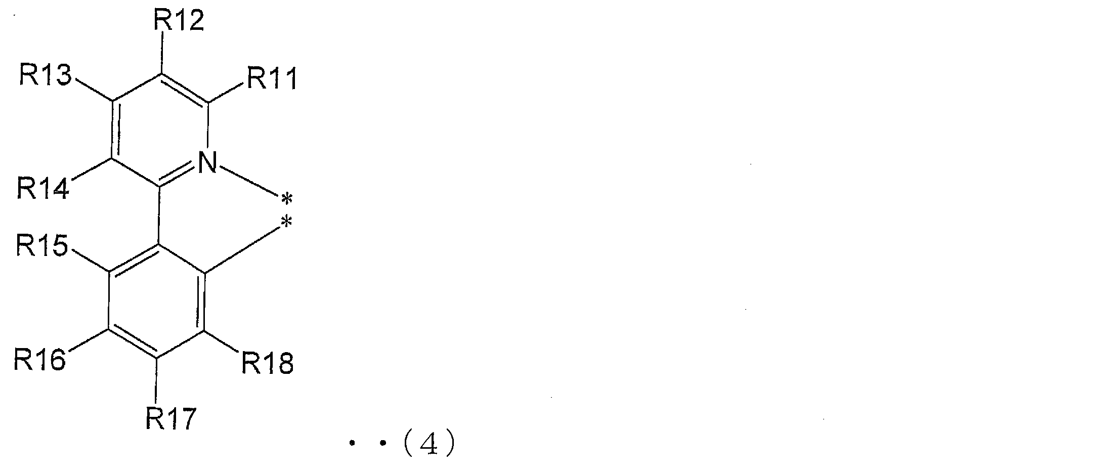
一般式(4)中、R11~R18は互いに独立して、水素原子;ハロゲン原子;又は炭素数1~10個の炭化水素基;を表す。ここで、当該炭化水素基に含まれる炭素数は好ましくは1~5個である。また、当該炭化水素基に含まれる少なくとも一つの水素原子は、フッ素、塩素、臭素及びヨウ素等のハロゲン原子で置換されていてもよい。また、当該炭化水素基が2個以上の炭素原子を含む場合に、当該炭素原子の一部が硫黄原子又は窒素原子で置換されていてもよい。さらに、炭化水素基同士(より好ましくは、隣接する炭化水素基である(i)R11とR12、(ii)R12とR13、(iii)R13とR14、(iv)R14とR15、(v)R15とR16、(vi)R16とR17、及び(vii)R17とR18、から選択される少なくとも一組)は互いに連結して、芳香族環、飽和又は不飽和の炭化水素環(芳香族環を除く)、或いは、硫黄原子及び/又は窒素原子(ヘテロ原子)を含んだ複素環を構成してもよい。なお、式中、*はMへの配位を示す。
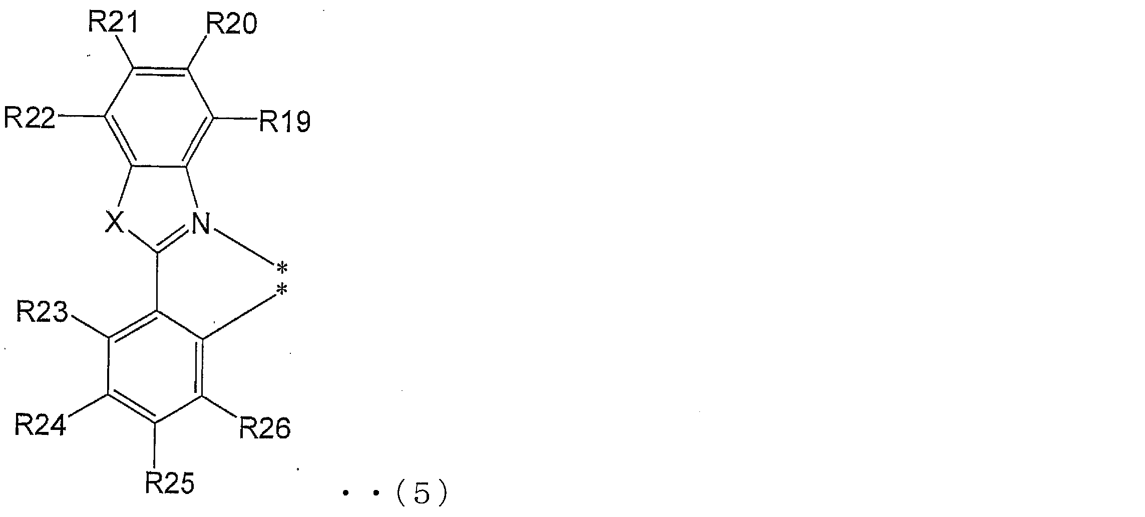
一般式(5)中、Xは酸素原子又は硫黄原子を表し、R19~R26は互いに独立して、水素原子;ハロゲン原子;又は炭素数1~10個の炭化水素基;を表す。ここで、当該炭化水素基に含まれる炭素数は好ましくは1~5個である。また、当該炭化水素基に含まれる少なくとも一つの水素原子は、フッ素、塩素、臭素及びヨウ素等のハロゲン原子で置換されていてもよい。また、当該炭化水素基が2個以上の炭素原子を含む場合に、当該炭素原子の一部が硫黄原子又は窒素原子で置換されていてもよい。さらに、炭化水素基同士(より好ましくは、隣接する炭化水素基である(i)R19とR20、(ii)R20とR21、(iii)R21とR22、(vi)R23とR24、(v)R24とR25、及び(vi)R25とR26、から選択される少なくとも一組)は互いに連結して、芳香族環、飽和又は不飽和の炭化水素環(芳香族環を除く)、或いは、硫黄原子及び/又は窒素原子(ヘテロ原子)を含んだ複素環を構成してもよい。なお、式中、*はMへの配位を示す。

一般式(6)中、R27~R33は互いに独立して、水素原子;ハロゲン原子;又は炭素数1~10個の炭化水素基;を表す。ここで、当該炭化水素基に含まれる炭素数は好ましくは1~5個である。また、当該炭化水素基に含まれる少なくとも一つの水素原子は、フッ素、塩素、臭素、ヨウ素等のハロゲン原子で置換されていてもよい。また、当該炭化水素基が2個以上の炭素原子を含む場合に、当該炭素原子の一部が硫黄原子又は窒素原子で置換されていてもよい。さらに、炭化水素基同士(より好ましくは、隣接する炭化水素基である(i)R27とR28、(ii)R28とR29、(iii)R29とR30、(vi)R30とR31、(v)R31とR32、及び(vi)R32とR33、から選択される少なくとも一組)は互いに連結して、芳香族環、飽和又は不飽和の炭化水素環(芳香族環を除く)、或いは、硫黄原子及び/又は窒素原子(ヘテロ原子)を含んだ複素環を構成してもよい。なお、式中、*はMへの配位を示す。
また、上記一般式(1)中、中心金属Mは、遷移金属原子から任意に選択される金属であり、例えば、イリジウム(Ir)、白金、パラジウム、ロジウム、レニウム、ルテニウム、オスミウム、タリウム、鉛、ビスマス、インジウム、スズ、アンチモン、テルル、金、及び銀等が挙げられ、中でもイリジウム、オスミウム及び白金のいずれかがより好ましく、イリジウムが特に好ましい。
また、上記一般式(1)中、m及びnはいずれも1以上の整数であり、mとnとの合計は、中心金属Mに配位することができる配位子の最大数以下、好ましくは当該最大数と同数である。中心金属Mの種類にもよるが、より優れた発光特性を得るためにはnが1であり、mが(中心金属Mに配位することができる配位子の最大数-1)であることがより好ましい。例えば、中心金属Mがイリジウムの場合、mとnとの合計は3以下になるので、nが1であり、mが2であることが好ましい。
このような新規錯体化合物として、特に限定されるものではないが、具体的には例えば、以下の化学式(28)~(31)に記載の錯体化合物が挙げられる。なお、化学式(28)に示す新規錯体化合物ビス(2-フェニルピリジン)イリジウム(III)(ジピリジルアミド)をIr(ppy)2-(dpa)と称し、化学式(29)に示す新規錯体化合物ビス(フェニルピラゾール)イリジウム(III)(ジピリジルアミド)をIr(ppz)2-(dpa)と称し、化学式(30)に示す新規錯体化合物ビス(2,4-(ジフルオロフェニル)ピラゾール)イリジウム(III)(ジピリジルアミド)をIr(dfppz)2-(dpa)と称し、化学式(31)に示す新規錯体化合物ビス(2,4-(ジフルオロフェニル)-3,5-ジメチルピラゾール)イリジウム(III)(ジピリジルアミド)をIr(dfmppz)2-(dpa)と称する。Ir(ppy)2-(dpa)、Ir(ppz)2-(dpa)、Ir(dfppz)2-(dpa)及びIr(dfmppz)2-(dpa)は順に、シクロメタル化配位子として、2-フェニルピリジン、フェニルピラゾール、2,4-(ジフルオロフェニル)ピラゾール及び2,4-(ジフルオロフェニル)-3,5-ジメチルピラゾールを用いたものである。また、いずれの新規錯体化合物も、補助配位子としてジピリジルアミドを用いたものである。


〔製造方法〕
本発明に係る錯体化合物は、上記のシクロメタル化配位子を中心金属Mに配位させて一次金属錯体を得る工程(1)と、次いで、上記の補助配位子を当該一次金属錯体に配位させて本発明に係る錯体化合物を得る工程(2)と、を含んでなる方法により製造される。この方法は、二段階の配位形成という簡単な反応であり、かつ簡単な化学構造の補助配位子を用いるために、発光特性に優れた化合物を容易に合成できるという利点がある。
本発明に係る錯体化合物は、上記のシクロメタル化配位子を中心金属Mに配位させて一次金属錯体を得る工程(1)と、次いで、上記の補助配位子を当該一次金属錯体に配位させて本発明に係る錯体化合物を得る工程(2)と、を含んでなる方法により製造される。この方法は、二段階の配位形成という簡単な反応であり、かつ簡単な化学構造の補助配位子を用いるために、発光特性に優れた化合物を容易に合成できるという利点がある。
上記の一次金属錯体を得る工程(1)は、例えば、中心金属Mのハロゲン化物(金属塩化物など)とシクロメタル化配位子とを、両者が充分に配位する程度の時間及び条件で共存させればよく、例えば、M. Nonoyama, Bull. Chem. Soc. Jpn. 1974, 47, 767.等に記載の公知の方法を参照して行うことができる。
工程(1)では、中心金属Mのハロゲン化物1モル当量に対して、過剰量のシクロメタル化配位子を共存させればよく、より具体的には、一般式(1)中のmに相当する当量以上のシクロメタル化配位子を共存させればよい。例えば、中心金属Mがイリジウムである場合には、イリジウムのハロゲン化物1モル当量に対して、2モル当量以上、より好ましくは2.5~3モル当量のシクロメタル化配位子を共存させればよい。
工程(1)は、中心金属Mのハロゲン化物及びシクロメタル化配位子に対して反応性を有しない溶媒中で行うことができ、このような溶媒として例えば、2-メトキシエタノール、テトラヒドロフラン(THF)、エトキシエタノール、等が挙げられる。また、必要に応じて、これら溶媒と水とを混合したものを溶媒として用いることもできる。さらに、必要に応じて、溶媒の還流を行ってもよい。
工程(1)の反応温度、反応圧力は常温及び常圧でよいが、上記した溶媒の還流を行う場合などは、例えば溶媒の蒸発が可能な温度及び圧力下で行ってもよい。
上記の工程(2)は、例えば、工程(1)で得られた一次金属錯体と補助配位子とを、両者が充分に配位する程度の時間及び条件で共存させればよい。式(30)に示す錯体化合物を製造する場合は、当該化合物を高選択的に製造できる点から、室温で反応させることが好ましい。
補助配位子は、下記一般式(20)で表される化合物からプロトンを引き抜いてアニオン化することで得ることができる。例えば、下記一般式(20)で表される化合物とn-BuLiとを共存させて、下記一般式(20)で表される化合物をリチウム化(アミド化)することで、補助配位子を得ることができる。なお、プロトンを引き抜く塩基としては、n-BuLiに限定されるものではなく、例えば、NaH及びKHなどのアルカリ金属水素化物を用いることもできる。
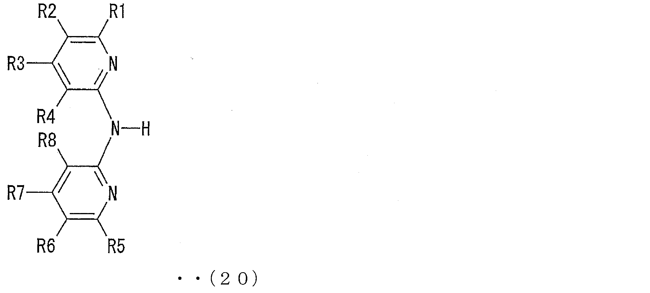
上記一般式(20)中のR1~R8の定義は、上記一般式(2)及び(3)にて説明したものと同一である。
上記一般式(20)で表される化合物として、具体的には例えば、下記の化学式(21)~(26)に示す化合物が挙げられるが、これらに限定されるものではない。

工程(2)では、中心金属Mのハロゲン化物1モル当量に対して、過剰量の補助配位子を共存させればよく、より具体的には、一般式(1)中のnに相当する当量以上の補助配位子を共存させればよい。例えば、中心金属Mがイリジウムである場合には、当該イリジウム1モル当量に対して、1モル当量以上、より好ましくは1.5~2モル当量の補助配位子を共存させればよい。
工程(2)は、中心金属Mのハロゲン化物及び補助配位子に対して反応性を有しない溶媒中で行うことができ、このような溶媒として例えば、2-メトキシエタノール、テトラヒドロフラン、及びエトキシエタノール等が挙げられる。また、必要に応じて、これら溶媒と水とを混合したものを溶媒として用いることもできる。さらに、必要に応じて、溶媒の還流を行ってもよい。
工程(2)の反応温度、反応圧力は常温・常圧でよいが、上記した溶媒の還流を行う場合などは、例えば溶媒の蒸発が可能な温度及び圧力下で行ってもよい。また、生成物の酸化を防止するために、工程(2)はアルゴン等の不活性ガスの雰囲気下で行うことが好ましい。
また、工程(1)及び(2)に加えて、反応生成物を精製する工程、その他の工程を適宜含むこともできる。
中心金属Mがイリジウムであり、補助配位子として2,2-ジピリジルアミドを用いた場合の合成スキームの概略を一例として以下の一般式(27)に示す。なお、この合成スキームの理解のために、後述する実施例の記載も参酌できる。

〔新規錯体化合物の用途〕
本発明に係る新規錯体化合物は、真空蒸着が可能であることから、その用途の一例として、有機発光素子(OLEDs:Organic Light-Emitting Devices)の発光材料が挙げられる。また、発光する性質を利用した検出マーカーとしての用途も考えられる。当該新規錯体化合物は、例えば、1)補助配位子中のNが持つ孤立電子対により潜在的な正孔輸送能を持つと考えられる点、2)補助配位子による立体制御により、新規錯体化合物内或いは新規錯体化合物間における発光部位(シクロメタル化配位子)同士の相互作用が低減されると考えられる点、などの発光材料として有利な特徴を備える。
本発明に係る新規錯体化合物は、真空蒸着が可能であることから、その用途の一例として、有機発光素子(OLEDs:Organic Light-Emitting Devices)の発光材料が挙げられる。また、発光する性質を利用した検出マーカーとしての用途も考えられる。当該新規錯体化合物は、例えば、1)補助配位子中のNが持つ孤立電子対により潜在的な正孔輸送能を持つと考えられる点、2)補助配位子による立体制御により、新規錯体化合物内或いは新規錯体化合物間における発光部位(シクロメタル化配位子)同士の相互作用が低減されると考えられる点、などの発光材料として有利な特徴を備える。
また、後述の実施例にも示すとおり、1)電圧印加により室温下でも実用上充分なりん光を発光すること、2)当該りん光の発光寿命が極めて短く、自己消光が最低限に抑制されること、3)比較的低電圧の印加で発光すること(発光効率がよいこと)、4)比較的高密度電流下でも発光効率が低下しにくく耐久性に優れること等の特性を示し、電圧印加による発光材料として特に適している。より具体的には、有機エレクトロルミネセンス(EL)素子等の発光材料、電圧印加による発光の有無を指標に対象物を検出する検出マーカー等として特に適している。
有機EL表示パネル(有機EL素子の一例)は、液晶表示パネルと比較して、高速応答で動画再生に適しており、かつより薄型化が可能という特徴を有する。その反面、電圧印加による発光材料の劣化、及び発光効率等が大きな課題となっている。特に、表示パネルを高精細化すれば各画素が小さくなるので、実用上充分な輝度を確保するために、より高電圧を発光材料に印加する必要が生じるという問題がある。そこで、本発明に係る新規錯体化合物を発光材料として用いれば、例えば、製品寿命が長く、発光効率に優れ、低消費電力で、かつ高精細(例えばVGA以上)な有機EL表示パネルの提供が可能となる。
本発明はさらに、一対の電極と、この電極間に配された発光材料を含む発光層とを含んでなり、当該発光層が本発明に係る化合物を含んでなる発光素子(有機EL素子)を提供する。以下、有機EL素子について具体的に説明する。
上記有機EL素子における電極は、正極と負極とを少なくとも含んでなる。正極は特に限定されないが、通常、発光層の光を外に取り出すために、ITO(Indium-Tin Oxide)等の透明電極が用いられる。
上記負極は特に限定されないが、例えば、アルミニウム電極を用いることができる。上記正極および負極の厚さは特に限定されないが、例えば、50nm以上400nm以下、好ましくは100nm以上300nm以下の範囲内である。上記正極および負極の抵抗値は、例えば5Ω以上50Ω以下、好ましくは10Ω以上30Ω以下の範囲内である。
上記発光層は、発光材料として本発明に係る化合物を含んでなる。当該発光層は蒸着法、及びキャストフィルム法等、薄膜を形成するための公知の方法で形成することができ、中でも蒸着法が好ましい。発光層の厚さは特に限定されないが、例えば、20nm以上40nm以下、好ましくは30nm以上40nm以下の範囲内である。
上記発光層は発光材料として本発明に係る化合物のみを含んでもよく、発光材料として他の化合物をさらに含んでいてもよい。例えば、本発明に係る化合物を発光ドーパントとし、発光ホスト中にドープする構成であってもよい。
本発明に係る化合物を発光ドーパントとする場合、発光ドーパントと発光ホストとの含有比は、所望する発光特性に応じて適宜設定すればよい。特に限定されないが、発光材料に占める発光ドーパントの割合を3重量%以上80重量%以下の範囲内とすることが好ましく、5重量%以上40重量%以下の範囲内とすることがより好ましく、5重量%以上20重量%以下の範囲内とすることがさらに好ましい。なお、発光ホストとしては4,4′-N,N′-ジカルバゾール-ビフェニル(CBP)等の公知のものを適宜利用すればよい。
本発明の化合物(発光ドーパント)を発光ホスト中にドープする構成をとれば、発光ホストの種類又はドープ量に応じて発光特性(発光波長等)を適宜変更することができる。
一方、本発明に係る化合物のみを発光材料として用いる場合には、1)発光層の形成が容易であり、かつ、2)発光ドーパントと発光ホストとの相分離の問題が生じない(すなわち品質劣化の虞が低減される)という利点がある。なお、発光ホストに発光ドーパントをドープするタイプのOLEDsをドープ型OLEDsと称し、一種類の発光材料のみからなる(ドープ構造をとらない)OLEDsを非ドープ型OLEDsと称する。
なお、上記の非ドープ型構造をとる場合は、本発明の化合物に含まれるシクロメタル化配位子の種類を変更することにより発光特性(発光波長等)を適宜変更できる。
上記有機EL素子は、発光層での正孔及び電子の再結合を促進するために、必要に応じて公知材料からなる正孔注入層、正孔輸送層、正孔阻止層、電子輸送層、電子注入層等をさらに含んでもよい。有機EL素子がこれらの層を全て含む場合、基板/電極(正極)/正孔注入層/正孔輸送層/発光層/正孔阻止層/電子輸送層/電子注入層/電極(負極)の順に積層される。
以下に実施例を示し、本発明の実施の形態についてさらに詳しく説明する。もちろん、本発明は以下の実施例に限定されるものではなく、細部については様々な態様が可能であることはいうまでもない。さらに、本発明は上述した実施形態に限定されるものではなく、請求項に示した範囲で種々の変更が可能であり、それぞれ開示された技術的手段を適宜組み合わせて得られる実施形態についても本発明の技術的範囲に含まれる。また、本明細書中に記載された文献の全てが参考として援用される。
以下、実施例により本発明を具体的に説明するが、本発明はこれに限定されない。
〔実施例1:Ir(ppy)2-(dpa)の合成、その構造の解析〕
(シクロメタル化Ir(III)μ-塩化物架橋前駆物質の合成)
一般式C^N2Ir(μ-Cl)2IrC^N2で表されるシクロメタル化Ir(III)μ-塩化物架橋二量体(一次金属錯体)は、Nonoyamaらの手法(M.Nonoyama, Bull. Chem. Soc. Jpn. 1974, 47, 767.を参照)を改良した方法に従い合成した。
(シクロメタル化Ir(III)μ-塩化物架橋前駆物質の合成)
一般式C^N2Ir(μ-Cl)2IrC^N2で表されるシクロメタル化Ir(III)μ-塩化物架橋二量体(一次金属錯体)は、Nonoyamaらの手法(M.Nonoyama, Bull. Chem. Soc. Jpn. 1974, 47, 767.を参照)を改良した方法に従い合成した。
具体的には、2-メトキシエタノールと水とを3:1の割合で含む溶媒中で、1モル当量のIrCl3・nH2O(7mmol,2.5g)と2.5モル当量のシクロメタル化配位子(2.8gのフェニルピリジン)とを共存させて、6~7時間還流した。次いで、反応混合物を室温まで冷却した後に加水し、反応生成物を沈降させた。
次いで、沈降物(反応生成物)を含む反応混合物をブフナーロートでろ過した。次いで、ろ過にて得られた残留物をヘキサンとエチルエーテルとで数回洗浄して粗精製物を得た。フェニルピリジン配位子を含むμ-塩化物架橋二量体([Ir(ppy)2(μ-Cl)]2)の収率は80%であった。なお、得られたμ-塩化物架橋二量体をNMR分析し、目的物であることを確認した。以下に分析の結果を示す。
1H NMR (300 MHz, CD2Cl2, rt) [Ir(ppy)2(μ-Cl]2: δ (ppm)= 9.13 (d, J=5.50 Hz, 4 H), 7.82 (d, J=7.70 Hz, 4 H), 7.69 (t, J=7.33Hz, 4 H), 7.44 (d, J=7.70 Hz,4 H), 6.66- 6.70 (m, 8 H), 6.50 (t, J=7.15 Hz, 4 H), 5.76 (d, J=7.33 Hz, 4H)。
1H NMR (300 MHz, CD2Cl2, rt) [Ir(ppy)2(μ-Cl]2: δ (ppm)= 9.13 (d, J=5.50 Hz, 4 H), 7.82 (d, J=7.70 Hz, 4 H), 7.69 (t, J=7.33Hz, 4 H), 7.44 (d, J=7.70 Hz,4 H), 6.66- 6.70 (m, 8 H), 6.50 (t, J=7.15 Hz, 4 H), 5.76 (d, J=7.33 Hz, 4H)。
(Ir(ppy)2-(dpa)の合成)
容積50mlのフラスコに、ヘキサン溶媒に溶解した2.6Mのn-BuLi(0.15mL)と、2,2’-ジピリジルアミン(68.48mg,0.4mmol)とを共存させて、室温で約2時間攪拌し、2,2’-ジピリジルアミンのリチウム化を行った。次いで、得られたN-リチウムジピリジルアミドを、15mLのTHFに溶解した[Ir(ppy)2(μ-Cl)]2(220mg,0.2mmol)中に滴下した。窒素雰囲気下、80℃で16時間攪拌した後、反応混合物を室温まで冷却し、溶媒を真空蒸発させた。THFを完全に取り除くために、残留物をトルエンに溶解し、減圧下で溶媒を蒸発させた。反応生成物を再度トルエンに溶解してろ過し、塩化リチウムを取り除いた。粗生成物をジエチルエーテルで洗浄して、下記化学式(28)で示される本発明に係る新規なイリジウム錯体Ir(ppy)2-(dpa)を70%の収率で得た。得られた新規なイリジウム錯体をNMR分析し、目的物であることを確認した。以下に分析の結果を示す。
1H NMR (300 MHz, C4D8O2, rt): N-Litho-dipyridylamido: δ(ppm)= 7.94 (d, J=3.20, 2 H), 7.23 (t, J=7.33, 2 H), 7.0 (d, J=8.43, 2 H), 6.27 (t, J=5.67 Hz, 2 H).1H NMR(300MHz, C4D8O2,rt): [Ir(ppy)2-(dpa]: δ(ppm) = 8.36 (d, J=5.50 Hz, 2 H), 7.94 (d, J=8.06 Hz, 2 H ), 7.73 (t, J=7.33 Hz, 2 H), 7.58(d, J=7.70 Hz, 2 H), 7.15 (d, J=5.06 Hz, 2 H), 7.05-6.97(m, 4 H), 6.75 (t, J=7.33 Hz, 2 H), 6.61 (d, J=6.60 Hz, 4 H), 6.12 (d, J=7.33 Hz, 2 H), 5.75 (t, J=6.04 Hz, 2 H).13C NMR (75 MHz, C4D8O2, rt): [Ir(ppy)2-(dpa]: δ(ppm) = 168.56, 155.61, 155.57,
149.55, 144.24,149.11, 136.91, 134.04, 131.77, 129.35, 124.18, 123.35, 122.03, 120.67, 118.91, 110.90。
容積50mlのフラスコに、ヘキサン溶媒に溶解した2.6Mのn-BuLi(0.15mL)と、2,2’-ジピリジルアミン(68.48mg,0.4mmol)とを共存させて、室温で約2時間攪拌し、2,2’-ジピリジルアミンのリチウム化を行った。次いで、得られたN-リチウムジピリジルアミドを、15mLのTHFに溶解した[Ir(ppy)2(μ-Cl)]2(220mg,0.2mmol)中に滴下した。窒素雰囲気下、80℃で16時間攪拌した後、反応混合物を室温まで冷却し、溶媒を真空蒸発させた。THFを完全に取り除くために、残留物をトルエンに溶解し、減圧下で溶媒を蒸発させた。反応生成物を再度トルエンに溶解してろ過し、塩化リチウムを取り除いた。粗生成物をジエチルエーテルで洗浄して、下記化学式(28)で示される本発明に係る新規なイリジウム錯体Ir(ppy)2-(dpa)を70%の収率で得た。得られた新規なイリジウム錯体をNMR分析し、目的物であることを確認した。以下に分析の結果を示す。
1H NMR (300 MHz, C4D8O2, rt): N-Litho-dipyridylamido: δ(ppm)= 7.94 (d, J=3.20, 2 H), 7.23 (t, J=7.33, 2 H), 7.0 (d, J=8.43, 2 H), 6.27 (t, J=5.67 Hz, 2 H).1H NMR(300MHz, C4D8O2,rt): [Ir(ppy)2-(dpa]: δ(ppm) = 8.36 (d, J=5.50 Hz, 2 H), 7.94 (d, J=8.06 Hz, 2 H ), 7.73 (t, J=7.33 Hz, 2 H), 7.58(d, J=7.70 Hz, 2 H), 7.15 (d, J=5.06 Hz, 2 H), 7.05-6.97(m, 4 H), 6.75 (t, J=7.33 Hz, 2 H), 6.61 (d, J=6.60 Hz, 4 H), 6.12 (d, J=7.33 Hz, 2 H), 5.75 (t, J=6.04 Hz, 2 H).13C NMR (75 MHz, C4D8O2, rt): [Ir(ppy)2-(dpa]: δ(ppm) = 168.56, 155.61, 155.57,
149.55, 144.24,149.11, 136.91, 134.04, 131.77, 129.35, 124.18, 123.35, 122.03, 120.67, 118.91, 110.90。

(単結晶エックス線回折分析)
エックス線構造解析に適したIr(ppy)2-(dpa)の単結晶を得て、その構造を単結晶エックス線回折分析により確認した。エックス線回折データは、SMART APEX diffractometer(Mo Kα radiation, graphite monochromator)(株式会社Bruker製の商品名)(λ=0.71069Å)を用いて取得した。構造決定は、SHELXTL5.01vを用いた直接法で行った後に、F2に対するフルマトリックス最小二乗法により精密化した。
エックス線構造解析に適したIr(ppy)2-(dpa)の単結晶を得て、その構造を単結晶エックス線回折分析により確認した。エックス線回折データは、SMART APEX diffractometer(Mo Kα radiation, graphite monochromator)(株式会社Bruker製の商品名)(λ=0.71069Å)を用いて取得した。構造決定は、SHELXTL5.01vを用いた直接法で行った後に、F2に対するフルマトリックス最小二乗法により精密化した。
図1中の(a)は、Ir(ppy)2-(dpa)の単結晶構造の概略を示している。図1中の(b)は、Ir(ppy)2-(dpa)の結晶パッキングの概略を示している。図1中の(b)では、ピリジル環(ppy)が隣接分子のフェニル環上にあり、C2回転の関係にある最隣接分子の結晶パッキングを示している。隣接するフェニル環同士の平面間距離は約3.3Åである。
〔実施例2:Ir(ppy)2-(dpa)における吸収、フォトルミネセンス(PL)、及び電気化学的測定〕
(1)吸収スペクトル及びPLスペクトル
吸収スペクトルはUV-2550 UV-visスペクトロメータ(株式会社島津製作所製の商品名)を用いて取得した。PLスペクトルは、励起源としてキセノンアークランプを備えたRF5301PC蛍光スペクトロメータ(株式会社島津製作所製の商品名)を用いて記録した。
(1)吸収スペクトル及びPLスペクトル
吸収スペクトルはUV-2550 UV-visスペクトロメータ(株式会社島津製作所製の商品名)を用いて取得した。PLスペクトルは、励起源としてキセノンアークランプを備えたRF5301PC蛍光スペクトロメータ(株式会社島津製作所製の商品名)を用いて記録した。
(2)発光の量子収率
PLの量子収率は、350nmで励起したときの、1mol/l硫酸中の硫酸キニーネを標準(Φ =0.546)として測定した。測定には、イリジウム錯体をスペクトル分析グレードのCHCl3に溶解して新たに調製した溶液を使用した。量子収率の測定では±10%のエラーバーが得られた。
PLの量子収率は、350nmで励起したときの、1mol/l硫酸中の硫酸キニーネを標準(Φ =0.546)として測定した。測定には、イリジウム錯体をスペクトル分析グレードのCHCl3に溶解して新たに調製した溶液を使用した。量子収率の測定では±10%のエラーバーが得られた。
(3)発光寿命
発光寿命は、フェムト秒Ti:サファイアレーザシステム(Spectra-Physics, Spitfire)と組み合わせたストリークカメラベースシステムC4780(Hamamatsu社の商品名)を用いて測定した。励起波長は397nmとし、検出波長は450~700nmとした。時間分解能は30~40nsであった。発光寿命の測定では±10%のエラーバーが得られた。
発光寿命は、フェムト秒Ti:サファイアレーザシステム(Spectra-Physics, Spitfire)と組み合わせたストリークカメラベースシステムC4780(Hamamatsu社の商品名)を用いて測定した。励起波長は397nmとし、検出波長は450~700nmとした。時間分解能は30~40nsであった。発光寿命の測定では±10%のエラーバーが得られた。
(4)電気化学的測定
電気化学的測定には、サイクリック・ボルタンメトリーHSV-100(北斗電工社製)及びelectrochemical work stationを用いて行った。より具体的には、白金棒を動作電極(working electrode)に、白金線を補助電極(auxiliary electrode)に採用し、参照電極としてAg/AgNO3電極を採用し、フェロセン/フェロセニウム対に対して標準化し、スキャンレートを100mV/sとしてサイクリック・ボルタンメトリーにより行った。各測定は、内部標準である、フェロセン/フェロセニウム(Fc)酸化還元系により、較正した。Ir(ppy)2-(dpa)の電気化学的挙動は、フェロセンを内部標準として用い、サイクリック・ボルタンメトリーにより調べた。測定は、0.1MのTBAPを含むアセトニトリル溶媒中で行った。
電気化学的測定には、サイクリック・ボルタンメトリーHSV-100(北斗電工社製)及びelectrochemical work stationを用いて行った。より具体的には、白金棒を動作電極(working electrode)に、白金線を補助電極(auxiliary electrode)に採用し、参照電極としてAg/AgNO3電極を採用し、フェロセン/フェロセニウム対に対して標準化し、スキャンレートを100mV/sとしてサイクリック・ボルタンメトリーにより行った。各測定は、内部標準である、フェロセン/フェロセニウム(Fc)酸化還元系により、較正した。Ir(ppy)2-(dpa)の電気化学的挙動は、フェロセンを内部標準として用い、サイクリック・ボルタンメトリーにより調べた。測定は、0.1MのTBAPを含むアセトニトリル溶媒中で行った。
(5)熱安定性
熱安定性の測定は、熱重量測定装置TGA-50(島津社製)を用いて行った。より具体的には、2mgのサンプルをアルミパン上に載せ、10℃/分の速度で450℃まで昇温させて測定した。
熱安定性の測定は、熱重量測定装置TGA-50(島津社製)を用いて行った。より具体的には、2mgのサンプルをアルミパン上に載せ、10℃/分の速度で450℃まで昇温させて測定した。
(測定の結果)
(1)吸収スペクトル及びPLスペクトル
図2は、脱気したジクロロメタン中又は固相状態で観察した、新規なイリジウム錯体のUV-Vis吸収スペクトル及びPLスペクトルを示す。250~350nmにおける強い吸収は、シクロメタル化配位子上(IL)でスピンが許容されたILπ-π*遷移が関与している。350~400nmにおける比較的弱い吸収は、金属-配位子間電荷移動(MLCT:metal-ligand charge transfer)遷移に許容されたスピンによるものである。400~470nmにおける吸収は、MLCT及びπ-π*遷移が関与していると考えられる。
(1)吸収スペクトル及びPLスペクトル
図2は、脱気したジクロロメタン中又は固相状態で観察した、新規なイリジウム錯体のUV-Vis吸収スペクトル及びPLスペクトルを示す。250~350nmにおける強い吸収は、シクロメタル化配位子上(IL)でスピンが許容されたILπ-π*遷移が関与している。350~400nmにおける比較的弱い吸収は、金属-配位子間電荷移動(MLCT:metal-ligand charge transfer)遷移に許容されたスピンによるものである。400~470nmにおける吸収は、MLCT及びπ-π*遷移が関与していると考えられる。
イリジウム錯体Ir(ppy)2-(dpa)は、ジクロロメタン中において、青みがかった緑色の発光(emission)を示した。また、発光は、480nmの波長で極大値を示し、510nmの波長でショルダーピークを示した。上記イリジウム錯体の薄膜(固相状態に相当)でのPLスペクトルは、極大値が530nmとなる深色シフトを示し、より広範囲の発光となった。
この現象は、Ir(ppy)2-(dpa)錯体中の芳香族配位子間でのπ-π*相互作用を含め、固相状態での強い分子間相互作用が関与していると考えられる。
(2)発光寿命
りん光の発光寿命は、3重項-3重項崩壊の重要なファクターの一つである。りん光の発光寿命が長いほど、その材料は潜在的により多くの3重項-3重項崩壊を持つことが知られている。図3は、THF溶液中でのりん光発光の遅延時間を示す。THF溶液中、環境温度で、波長402nmの励起光を与えたときの、Ir(ppy)2-(dpa)のりん光の発光寿命は、0.17μsであった。これは陽イオン性錯体である、[Ir(ppy)2(Hdpa)]+、Ir(ppy)3、及びIr(ppy)2(acac)におけるりん光の発光寿命(それぞれ、2.1μs、1.9μs、及び1.6μs)に比べて極めて短い。すなわち、この新規なイリジウム錯体は、相対的に発光寿命が短く、自己消光が非常に弱いことが示されている。
りん光の発光寿命は、3重項-3重項崩壊の重要なファクターの一つである。りん光の発光寿命が長いほど、その材料は潜在的により多くの3重項-3重項崩壊を持つことが知られている。図3は、THF溶液中でのりん光発光の遅延時間を示す。THF溶液中、環境温度で、波長402nmの励起光を与えたときの、Ir(ppy)2-(dpa)のりん光の発光寿命は、0.17μsであった。これは陽イオン性錯体である、[Ir(ppy)2(Hdpa)]+、Ir(ppy)3、及びIr(ppy)2(acac)におけるりん光の発光寿命(それぞれ、2.1μs、1.9μs、及び1.6μs)に比べて極めて短い。すなわち、この新規なイリジウム錯体は、相対的に発光寿命が短く、自己消光が非常に弱いことが示されている。
(3)発光の量子収率
りん光発光の量子収率を指すCHCl3溶液中でのIr(ppy)2-(dpa)のΦpは、0.87であった。この値は、近い関係にある陽イオン性錯体である[Ir(ppy)2(Hdpa)][PF6]のΦp(0.43)、従来のイリジウム錯体であるIr(ppy)3のΦp(0.4)、及びIr(ppy)2(acac) のΦp(0.34)をはるかに上回る。
りん光発光の量子収率を指すCHCl3溶液中でのIr(ppy)2-(dpa)のΦpは、0.87であった。この値は、近い関係にある陽イオン性錯体である[Ir(ppy)2(Hdpa)][PF6]のΦp(0.43)、従来のイリジウム錯体であるIr(ppy)3のΦp(0.4)、及びIr(ppy)2(acac) のΦp(0.34)をはるかに上回る。
(4)電気化学的測定
電気化学的測定の結果を表1に示す。表1中で、還元ポテンシャルは、最適な吸収を示すオンセット波長から見積もった。また、参考までに、後述する実施例3で用いた材料NPB、CBP、BCP、及びAlQ(Alq3)に関して文献値を記載した。Ir(ppy)2-(dpa)の酸化ポテンシャルは1.04Vであった。図4は、アセトニトリル中でのサイクリックボルタモグラフを示す。
電気化学的測定の結果を表1に示す。表1中で、還元ポテンシャルは、最適な吸収を示すオンセット波長から見積もった。また、参考までに、後述する実施例3で用いた材料NPB、CBP、BCP、及びAlQ(Alq3)に関して文献値を記載した。Ir(ppy)2-(dpa)の酸化ポテンシャルは1.04Vであった。図4は、アセトニトリル中でのサイクリックボルタモグラフを示す。
(5)熱安定性
熱重量分析(TGA:thermo gravimetric analysis)の結果、Ir(ppy)2-(dpa)の分解開始温度(Td)は、約350℃であり、熱安定性に非常に優れていた。真空下では約200℃で昇華することが可能であるため、真空蒸着に対して十分な熱安定性を有していることが理解できる。
熱重量分析(TGA:thermo gravimetric analysis)の結果、Ir(ppy)2-(dpa)の分解開始温度(Td)は、約350℃であり、熱安定性に非常に優れていた。真空下では約200℃で昇華することが可能であるため、真空蒸着に対して十分な熱安定性を有していることが理解できる。
〔実施例3:Ir(ppy)2-(dpa)を用いたOLEDsの製造、エレクトロルミネセンス(EL)の測定〕
本発明に係るイリジウム錯体の発光特性を理解するため、この錯体を発光ホストとして用いた非ドープ型OLEDs(ここではダイオード)IVを製造した。まず、一面がITO(アノードになる)で被覆されたガラス基板(シート抵抗:20Ω/cm2)をパターニングし、次いで脱イオン水、アセトン及びイソプロピルアルコールにて、この順で20分ずつ超音波洗浄した後、流動窒素中で乾燥した。有機膜蒸着の前に、ITO表面に対して酸素プラズマ処理を15分間施した。次いで、ITOの膜上に有機物材料であるN,N’-ジフェニル-N,N’-ビス(1-ナフチル)-1,1’-ジフェニル-4,4’-ジアミン(NPB)、イリジウム錯体、2,9-ジメチル-4,7-ジフェニル-1,10-フェナントロリン(BCP)、及びトリス(8-ヒドロキシキノリン)アルミニウム(Alq3)を、この順に熱蒸着した。全ての有機物材料は、連続昇華方法により精製し、8×104Paの圧力下、1.0Å/sのレートで熱蒸着した。NPB、イリジウム錯体、BCP、及びAlQそれぞれの膜厚は、順に、30nm、25nm、6nm、及び20nmである。蒸着層の厚さは、水晶振動子モニターにより、インシチュ測定した。
本発明に係るイリジウム錯体の発光特性を理解するため、この錯体を発光ホストとして用いた非ドープ型OLEDs(ここではダイオード)IVを製造した。まず、一面がITO(アノードになる)で被覆されたガラス基板(シート抵抗:20Ω/cm2)をパターニングし、次いで脱イオン水、アセトン及びイソプロピルアルコールにて、この順で20分ずつ超音波洗浄した後、流動窒素中で乾燥した。有機膜蒸着の前に、ITO表面に対して酸素プラズマ処理を15分間施した。次いで、ITOの膜上に有機物材料であるN,N’-ジフェニル-N,N’-ビス(1-ナフチル)-1,1’-ジフェニル-4,4’-ジアミン(NPB)、イリジウム錯体、2,9-ジメチル-4,7-ジフェニル-1,10-フェナントロリン(BCP)、及びトリス(8-ヒドロキシキノリン)アルミニウム(Alq3)を、この順に熱蒸着した。全ての有機物材料は、連続昇華方法により精製し、8×104Paの圧力下、1.0Å/sのレートで熱蒸着した。NPB、イリジウム錯体、BCP、及びAlQそれぞれの膜厚は、順に、30nm、25nm、6nm、及び20nmである。蒸着層の厚さは、水晶振動子モニターにより、インシチュ測定した。
続いて、AlQの膜上に、厚さ1nmのフッ化リチウム(LiF)層を0.2Å/sのレートで真空蒸着した。最後にアルミニウム電極(カソードになる)を別の真空チャンバー内で、10Å/sのレートで真空蒸着し、ダイオードを作製した。
電極部分の作用面積は、5×5mm2であった。なお、上記NPB層は正孔輸送層として、イリジウム錯体層は発光層として、BCP層は正孔阻止層として、AlQ層は電子輸送層として、LiF層は電子注入層として、アルミニウム層は金属カソード層として機能している。これら材料の化学構造と、OLEDsの構造とを図5に示す。
(ドープ型OLEDsの作製)
一方、本発明に係るイリジウム錯体を発光ドーパントとし、発光ホストであるCBPにドープして、ドープ型OLEDsI~IIIを製造した。ドープ型OLEDsI~IIIの発光層の厚さはいずれも25nmで、順に、発光ドーパントとしてイリジウム錯体を5重量%、10重量%及び20重量%の濃度で含む。発光層の組成以外の構成及び作製方法は、上記非ドープ型OLEDsIVと共通である。
一方、本発明に係るイリジウム錯体を発光ドーパントとし、発光ホストであるCBPにドープして、ドープ型OLEDsI~IIIを製造した。ドープ型OLEDsI~IIIの発光層の厚さはいずれも25nmで、順に、発光ドーパントとしてイリジウム錯体を5重量%、10重量%及び20重量%の濃度で含む。発光層の組成以外の構成及び作製方法は、上記非ドープ型OLEDsIVと共通である。
(OLEDsI~IVのエレクトロルミネッセンス(EL)の測定)
作製されたOLEDsI~IVの、ELスペクトルは、室温において、高分解能スペクトロメータ(Stellar net Blue wave UV-VIS-NIR)を用いて測定した。作製されたOLEDsI~IVの、電流密度-電圧-輝度(I-V-L)特性は、室温において、輝度計Chroma-Meter CS-200(コニカミノルタ社製)及びKeithley2400プログラム制御電圧電流デジタルソースメータ(Keithley 2400 programmable voltage-current digital source meter)を用いて測定した。結果を図6及び図7に示す。
作製されたOLEDsI~IVの、ELスペクトルは、室温において、高分解能スペクトロメータ(Stellar net Blue wave UV-VIS-NIR)を用いて測定した。作製されたOLEDsI~IVの、電流密度-電圧-輝度(I-V-L)特性は、室温において、輝度計Chroma-Meter CS-200(コニカミノルタ社製)及びKeithley2400プログラム制御電圧電流デジタルソースメータ(Keithley 2400 programmable voltage-current digital source meter)を用いて測定した。結果を図6及び図7に示す。
(結果)
図6は各波長におけるEL強度を測定した結果を示した図であり、図7は、OLEDsIにおいて駆動電圧を変化させてEL強度を測定した結果を示した図である。OLEDsI~IVはいずれも、9Vの駆動電圧において緑色の発光を示した。また、OLEDsIは、印加した駆動電圧(6V~12V)に関わらず緑色の発光を示した。また、いずれのOLEDsにおいても、駆動電圧が高い場合であっても、ホスト層あるいは隣接層から別の発光が生じることはなかった。このことは、ホストの励起子からりん光体へ、エネルギー及び/又は電荷が完全に転移していることを示している。各OLEDsにおいて、電流及びバイアス電圧を変化させても、ELスペクトル及びCIE色度座標に有意な変化はみられなかった。
図6は各波長におけるEL強度を測定した結果を示した図であり、図7は、OLEDsIにおいて駆動電圧を変化させてEL強度を測定した結果を示した図である。OLEDsI~IVはいずれも、9Vの駆動電圧において緑色の発光を示した。また、OLEDsIは、印加した駆動電圧(6V~12V)に関わらず緑色の発光を示した。また、いずれのOLEDsにおいても、駆動電圧が高い場合であっても、ホスト層あるいは隣接層から別の発光が生じることはなかった。このことは、ホストの励起子からりん光体へ、エネルギー及び/又は電荷が完全に転移していることを示している。各OLEDsにおいて、電流及びバイアス電圧を変化させても、ELスペクトル及びCIE色度座標に有意な変化はみられなかった。
ドープ型OLEDsのELスペクトルの極大は、ドーパントの濃度が高くなるにつれ、513nmから530nmまでわずかにレッドシフトした。これは、PLスペクトルに見られるように、ドーパントの濃度が高いほど、より強力な分子間相互作用が生じるためであると考えられる。
図8は、OLEDsI~IVの輝度-電圧特性及び電流密度-電圧特性の測定結果を示す。非ドープ型OLEDsIVと比較して、ドープ型OLEDsI~IIIの駆動電圧はより低くなった。またドープ濃度が最も低いOLEDsIにおいて、駆動電圧が最も低くなった。OLEDsII~IVにおいては、電流密度-電圧特性に差は見られなかったが、ドープ濃度が最も低いOLEDsIは、他のOLEDsに比べ、電流密度-電圧特性に優れていた。
図9は、OLEDsI~IVの電流効率-電流密度特性及びエネルギー効率-電流密度特性の測定結果を示す。非ドープ型OLEDsIVと比較して、ドープ型OLEDsI~IIIは電流効率及びエネルギー効率に優れていた。特にドープ濃度が最も低いOLEDsIにおいては、電流密度2mA/cm2における電流効率及びエネルギー効率が、それぞれ120cd/A及び43lm/Wとなり、OLEDsI~IVにおいて最も高かった。OLEDsI~IVにおけるこれらの値は、Ir(III)をCBPにドープしたこれまでに報告されている緑色発光素子(次の文献を参照。Baldo M. A. et al, Appl. Phys. Lett., 1999, 75, 4; Lamansky S. et al, J. Am. Chem. Soc., 2001, 123, 4304; Liu Y.et al, Chem. Commun., 2009, 25, 3699)と比較してより高い値であった。また、OLEDsIでは、高い電流密度(94mA/cm2)においても、優れた電流効率(39cd/A)及びエネルギー効率(6.8lm/W)を示した。
各OLEDsの特性をまとめた表を表2に示す。

次に、3重量%のドープ濃度のOLEDsVを作製し、さらなる検討を行った。結果を図10~図12に示す。図10は、駆動電圧を変化させてEL強度を測定した結果を示した図である。図10に示すように、OLEDsVにおいても印加した駆動電圧に関わらず、緑色の発光を示した。図11は、輝度-電圧特性及び電流密度-電圧特性の測定結果を示す。OLEDsI~IVと比較して(図8参照)、OLEDsVの輝度及び電流は低かった。図12は、OLEDsVの電流効率-電流密度特性及びエネルギー効率-電流密度特性の測定結果を示す。OLEDsVの電流効率-電流密度特性及びエネルギー効率-電流密度特性は、OLEDsI~IVの電流効率-電流密度特性及びエネルギー効率-電流密度特性と比較して(図9参照)、いずれも低かった。
〔実施例4:Ir(ppz)2-(dpa)の合成、その構造の解析〕
(シクロメタル化Ir(III)μ-塩化物架橋前駆物質の合成)
反応に使用するシクロメタル化配位子として0.211gのフェニルピラゾールを用いた以外は、実施例1と同様にして、シクロメタル化Ir(III)μ-塩化物架橋二量体(一次金属錯体)を合成した。フェニルピラゾール配位子を含むμ-塩化物架橋二量体([Ir(ppz)2(μ-Cl)]2)の収率は85%であった。なお、得られたμ-塩化物架橋二量体をNMR分析し、目的物であることを確認した。
(シクロメタル化Ir(III)μ-塩化物架橋前駆物質の合成)
反応に使用するシクロメタル化配位子として0.211gのフェニルピラゾールを用いた以外は、実施例1と同様にして、シクロメタル化Ir(III)μ-塩化物架橋二量体(一次金属錯体)を合成した。フェニルピラゾール配位子を含むμ-塩化物架橋二量体([Ir(ppz)2(μ-Cl)]2)の収率は85%であった。なお、得られたμ-塩化物架橋二量体をNMR分析し、目的物であることを確認した。
(Ir(ppz)2-(dpa)の合成)
反応に使用する一次金属錯体として[Ir(ppz)2(μ-Cl)]2を用いた以外は、実施例1と同様にして、下記化学式(29)で表される本発明に係る新規なイリジウム錯体Ir(ppz)2-(dpa)を合成した。Ir(ppz)2-(dpa)の収率は65%であった。得られた新規なイリジウム錯体をNMR分析し、目的物であることを確認した。以下に分析の結果を示す。
1H NMR (300MHz, C4D8O, rt): Ir(ppz)2-(dpa) δ= 8.36 (d, J=2.0 Hz, 2H), 7.43 (d,J= 2H), 7.30 (t, J=6.0 Hz, 4H) 7.05 (t, J=6.5 Hz, 2H), 6.76 (t, J= 7.5 Hz, 2 H), 6.76 ( t, J= 7.5 Hz, 2H), 6.62-6.51 (m, 4 H), 6.05 (d, J=7.0 Hz, 2H), 5.80 (t, J= 5.5 Hz, 2H)。
反応に使用する一次金属錯体として[Ir(ppz)2(μ-Cl)]2を用いた以外は、実施例1と同様にして、下記化学式(29)で表される本発明に係る新規なイリジウム錯体Ir(ppz)2-(dpa)を合成した。Ir(ppz)2-(dpa)の収率は65%であった。得られた新規なイリジウム錯体をNMR分析し、目的物であることを確認した。以下に分析の結果を示す。
1H NMR (300MHz, C4D8O, rt): Ir(ppz)2-(dpa) δ= 8.36 (d, J=2.0 Hz, 2H), 7.43 (d,J= 2H), 7.30 (t, J=6.0 Hz, 4H) 7.05 (t, J=6.5 Hz, 2H), 6.76 (t, J= 7.5 Hz, 2 H), 6.76 ( t, J= 7.5 Hz, 2H), 6.62-6.51 (m, 4 H), 6.05 (d, J=7.0 Hz, 2H), 5.80 (t, J= 5.5 Hz, 2H)。
〔実施例5:Ir(ppz)2-(dpa)におけるPLスペクトルの測定〕
実施例2と同様にして、Ir(ppz)2-(dpa)のPLスペクトルを測定した。測定結果を図13に示す。図13は、脱気したジクロロメタン中で観察した、Ir(ppz)2-(dpa)のPLスペクトルを示す。図13に示すとおり、Ir(ppz)2-(dpa)は、492nmの波長でPL極大値を示した。
実施例2と同様にして、Ir(ppz)2-(dpa)のPLスペクトルを測定した。測定結果を図13に示す。図13は、脱気したジクロロメタン中で観察した、Ir(ppz)2-(dpa)のPLスペクトルを示す。図13に示すとおり、Ir(ppz)2-(dpa)は、492nmの波長でPL極大値を示した。
〔実施例6:Ir(dfppz)2-(dpa)の合成、その構造の解析〕
(シクロメタル化配位子の合成)
シクロメタル化配位子である2,4-(ジフルオロフェニル)ピラゾール(dfppz)は、Yangらの方法(非特許文献:C.-H. Yang et al, Inorg. Chem., 2005, 44, 7770-7780.を参照)を用いて合成した。
(シクロメタル化配位子の合成)
シクロメタル化配位子である2,4-(ジフルオロフェニル)ピラゾール(dfppz)は、Yangらの方法(非特許文献:C.-H. Yang et al, Inorg. Chem., 2005, 44, 7770-7780.を参照)を用いて合成した。
(シクロメタル化Ir(III)μ-塩化物架橋前駆物質の合成)
反応に使用するシクロメタル化配位子として0.984gの2,4-(ジフルオロフェニル)ピラゾールを用いた以外は、実施例1と同様にして、シクロメタル化Ir(III)μ-塩化物架橋二量体(一次金属錯体)を合成した。2,4-(ジフルオロフェニル)ピラゾール配位子を含むμ-塩化物架橋二量体([Ir(dfppz)2(μ-Cl)]2)の収率は80%であった。なお、得られたμ-塩化物架橋二量体をNMR分析し、目的物であることを確認した。
反応に使用するシクロメタル化配位子として0.984gの2,4-(ジフルオロフェニル)ピラゾールを用いた以外は、実施例1と同様にして、シクロメタル化Ir(III)μ-塩化物架橋二量体(一次金属錯体)を合成した。2,4-(ジフルオロフェニル)ピラゾール配位子を含むμ-塩化物架橋二量体([Ir(dfppz)2(μ-Cl)]2)の収率は80%であった。なお、得られたμ-塩化物架橋二量体をNMR分析し、目的物であることを確認した。
(Ir(dfppz)2-(dpa)の合成)
反応に使用する一次金属錯体として[Ir(dfppz)2(μ-Cl)]2を用い、反応を室温で行ったこと以外は、実施例1と同様にして、下記化学式(30)で示される本発明に係る新規なイリジウム錯体Ir(dfppz)2-(dpa)を合成した。Ir(dfppz)2-(dpa)の収率は75%であった。得られた新規なイリジウム錯体をNMR分析し、目的物であることを確認した。以下に分析の結果を示す。
1H NMR (CDCl3-300 MHz, rt) δ(ppm)=8.34(d, J=2.56 Hz, 2 H), 8.12 (d, J=8.79 Hz, 2 H), 7.58 (d, J= 1.46 Hz, 2 H), 7.51-7.42 (m, 2 H), 7.36-7.16 (m, 2 H), 7.08 (t, J=7.69 Hz, 1 H), 6.56-6.40 (m, 4 H), 5.94 (d, J=8.06 Hz, 1 H), 5.72(d, J=8.43 Hz, 2 H)。
反応に使用する一次金属錯体として[Ir(dfppz)2(μ-Cl)]2を用い、反応を室温で行ったこと以外は、実施例1と同様にして、下記化学式(30)で示される本発明に係る新規なイリジウム錯体Ir(dfppz)2-(dpa)を合成した。Ir(dfppz)2-(dpa)の収率は75%であった。得られた新規なイリジウム錯体をNMR分析し、目的物であることを確認した。以下に分析の結果を示す。
1H NMR (CDCl3-300 MHz, rt) δ(ppm)=8.34(d, J=2.56 Hz, 2 H), 8.12 (d, J=8.79 Hz, 2 H), 7.58 (d, J= 1.46 Hz, 2 H), 7.51-7.42 (m, 2 H), 7.36-7.16 (m, 2 H), 7.08 (t, J=7.69 Hz, 1 H), 6.56-6.40 (m, 4 H), 5.94 (d, J=8.06 Hz, 1 H), 5.72(d, J=8.43 Hz, 2 H)。

(単結晶エックス線回折分析)
実施例1と同様にして、Ir(dfppz)2-(dpa)の構造を単結晶エックス線回折分析により確認した。分析結果を図14に示す。
実施例1と同様にして、Ir(dfppz)2-(dpa)の構造を単結晶エックス線回折分析により確認した。分析結果を図14に示す。
〔実施例7:Ir(dfppz)2-(dpa)におけるPLスペクトルの測定〕
実施例2と同様にして、Ir(dfppz)2-(dpa)のPLスペクトルを測定した。測定結果を図15に示す。図15は、脱気したジクロロメタン中で観察した、Ir(dfppz)2-(dpa)のPLスペクトルを示す。図15に示すとおり、Ir(dfppz)2-(dpa)は、500nmの波長でPL極大値を示した。
実施例2と同様にして、Ir(dfppz)2-(dpa)のPLスペクトルを測定した。測定結果を図15に示す。図15は、脱気したジクロロメタン中で観察した、Ir(dfppz)2-(dpa)のPLスペクトルを示す。図15に示すとおり、Ir(dfppz)2-(dpa)は、500nmの波長でPL極大値を示した。
〔実施例8:Ir(dfmppz)2-(dpa)の合成、その構造の解析〕
(シクロメタル化配位子の合成)
シクロメタル化配位子である2,4-(ジフルオロフェニル)-3,5-ジメチルピラゾール(dfmppz)は、Yangらの方法(非特許文献:C.-H. Yang et al, Inorg. Chem., 2005, 44, 7770-7780.を参照)を用いて合成した。
(シクロメタル化配位子の合成)
シクロメタル化配位子である2,4-(ジフルオロフェニル)-3,5-ジメチルピラゾール(dfmppz)は、Yangらの方法(非特許文献:C.-H. Yang et al, Inorg. Chem., 2005, 44, 7770-7780.を参照)を用いて合成した。
(シクロメタル化Ir(III)μ-塩化物架橋前駆物質の合成)
反応に使用するシクロメタル化配位子として1.068gの2,4-(ジフルオロフェニル)-3,5-ジメチルピラゾールを用いた以外は、実施例1と同様にして、シクロメタル化Ir(III)μ-塩化物架橋二量体(一次金属錯体)を合成した。2,4-(ジフル
オロフェニル)-3,5-ジメチルピラゾール配位子を含むμ-塩化物架橋二量体([Ir(dfmppz)2(μ-Cl)]2)の収率は80%であった。なお、得られたμ-塩化物架橋二量体をNMR分析し、目的物であることを確認した。
反応に使用するシクロメタル化配位子として1.068gの2,4-(ジフルオロフェニル)-3,5-ジメチルピラゾールを用いた以外は、実施例1と同様にして、シクロメタル化Ir(III)μ-塩化物架橋二量体(一次金属錯体)を合成した。2,4-(ジフル
オロフェニル)-3,5-ジメチルピラゾール配位子を含むμ-塩化物架橋二量体([Ir(dfmppz)2(μ-Cl)]2)の収率は80%であった。なお、得られたμ-塩化物架橋二量体をNMR分析し、目的物であることを確認した。
(Ir(dfmppz)2-(dpa)の合成)
反応に使用する一次金属錯体として[Ir(dfmppz)2(μ-Cl)]2を用いた以外は、実施例1と同様にして、下記化学式(31)で表される本発明に係る新規なイリジウム錯体Ir(dfppz)2-(dpa)を合成した。Ir(dfmppz)2-(dpa)の収率は70%であった。得られた新規なイリジウム錯体をNMR分析し、目的物であることを確認した。以下に分析の結果を示す。1H NMR:(400 MHz, CDCl3, rt) δ=8.19 (d, J=8.70, 1H), 8.01-7.98(m, 1H), 7.42-7.38m, 1H), 6.96-6.92 (m, 2H), 6.57-6.51 (m,2H) 6.36-6.31(m, 2H), 6.26 (s, 1H), 6.20 (s, 1H), 5.74-5.72(m,2H), 5.62 (d, J=8.70 Hz , 1H), 2.73-2.65(m, 6H), 2.22(s, 3H, 1.86 (s, 3H)。
反応に使用する一次金属錯体として[Ir(dfmppz)2(μ-Cl)]2を用いた以外は、実施例1と同様にして、下記化学式(31)で表される本発明に係る新規なイリジウム錯体Ir(dfppz)2-(dpa)を合成した。Ir(dfmppz)2-(dpa)の収率は70%であった。得られた新規なイリジウム錯体をNMR分析し、目的物であることを確認した。以下に分析の結果を示す。1H NMR:(400 MHz, CDCl3, rt) δ=8.19 (d, J=8.70, 1H), 8.01-7.98(m, 1H), 7.42-7.38m, 1H), 6.96-6.92 (m, 2H), 6.57-6.51 (m,2H) 6.36-6.31(m, 2H), 6.26 (s, 1H), 6.20 (s, 1H), 5.74-5.72(m,2H), 5.62 (d, J=8.70 Hz , 1H), 2.73-2.65(m, 6H), 2.22(s, 3H, 1.86 (s, 3H)。
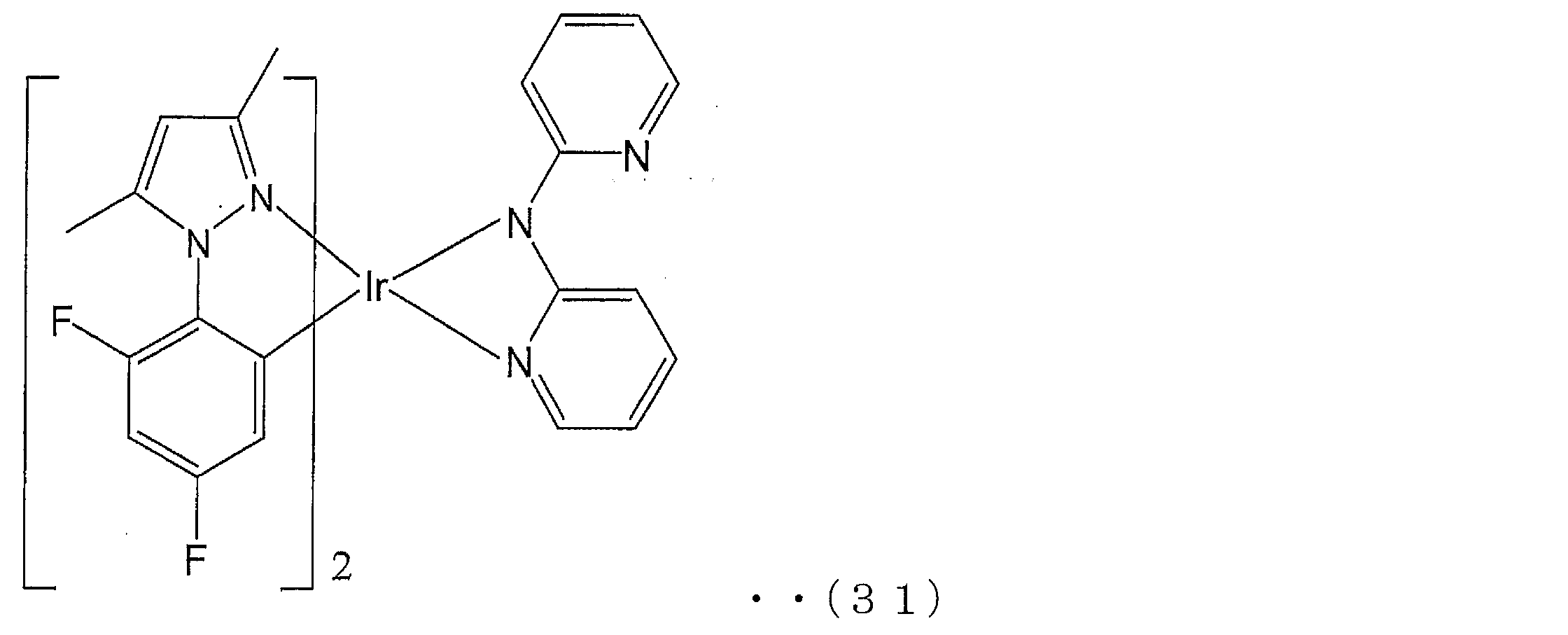
〔実施例9:Ir(dfmppz)2-(dpa)における吸収スペクトル及びPLスペクトルの測定〕
実施例2と同様にして、Ir(dfmppz)2-(dpa)のUV-Vis吸収スペクトル及びPLスペクトルを測定した。測定結果を図16に示す。図16は、脱気したジクロロメタン中で観察した、Ir(dfmppz)2-(dpa)のUV-Vis吸収スペクトル及びPLスペクトルを示す。図16に示すとおり、Ir(dfmppz)2-(dpa)は、505nmの波長でPL極大値を示し、450nmでショルダーピークを示した。
実施例2と同様にして、Ir(dfmppz)2-(dpa)のUV-Vis吸収スペクトル及びPLスペクトルを測定した。測定結果を図16に示す。図16は、脱気したジクロロメタン中で観察した、Ir(dfmppz)2-(dpa)のUV-Vis吸収スペクトル及びPLスペクトルを示す。図16に示すとおり、Ir(dfmppz)2-(dpa)は、505nmの波長でPL極大値を示し、450nmでショルダーピークを示した。
(単結晶エックス線回折分析)
実施例1と同様にして、Ir(dfmppz)2-(dpa)の構造を単結晶エックス線回折分析により確認した。分析結果を図17に示す。
実施例1と同様にして、Ir(dfmppz)2-(dpa)の構造を単結晶エックス線回折分析により確認した。分析結果を図17に示す。
本発明によれば、発光ドーパントとしてはもちろん、単独で使用した場合でも実用上充分な発光特性を示す新規錯体化合物、当該化合物を用いた発光方法、及び発光素子を提供することができる。本発明は、例えば、検出マーカー、又は有機エレクトロルミネセンス素子の発光材料として好適に利用可能である。
Claims (6)
- 下記一般式(1)で表されることを特徴とする錯体化合物。

mおよびnはいずれも1以上の整数であり、mとnとの合計は、Mに配位することができる配位子の最大数以下である。)
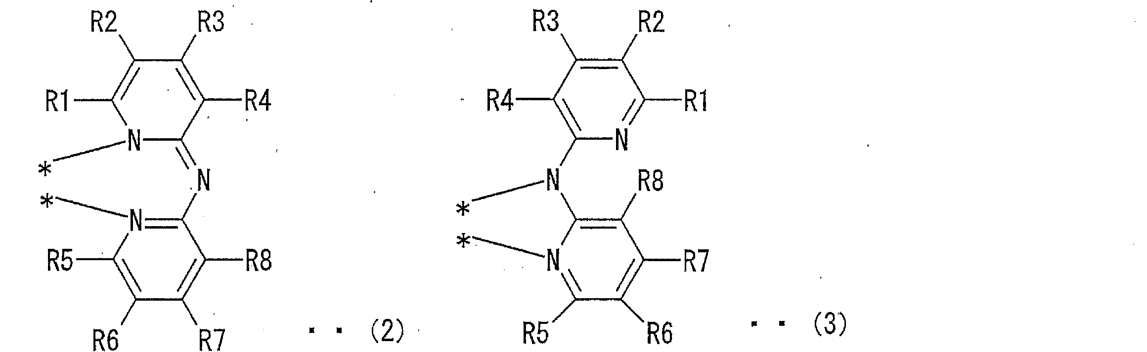
- 上記一般式(2)及び(3)中、R1とR5とは同一であり、R2とR6とは同一であり、R3とR7とは同一であり、R4とR8とは同一であることを特徴とする請求項1に記載の錯体化合物。
- 上記シクロメタル化配位子は、下記一般式(4)、下記一般式(5)又は下記一般式(6)で表されることを特徴とする請求項1又は2に記載の錯体化合物。
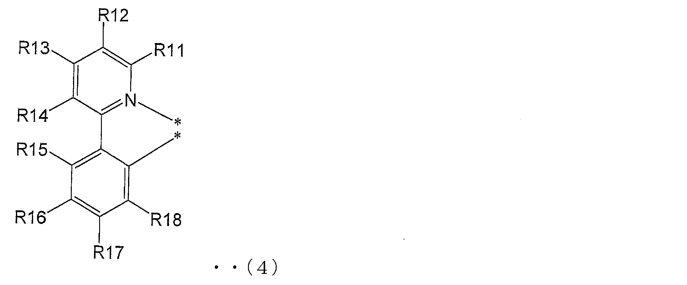
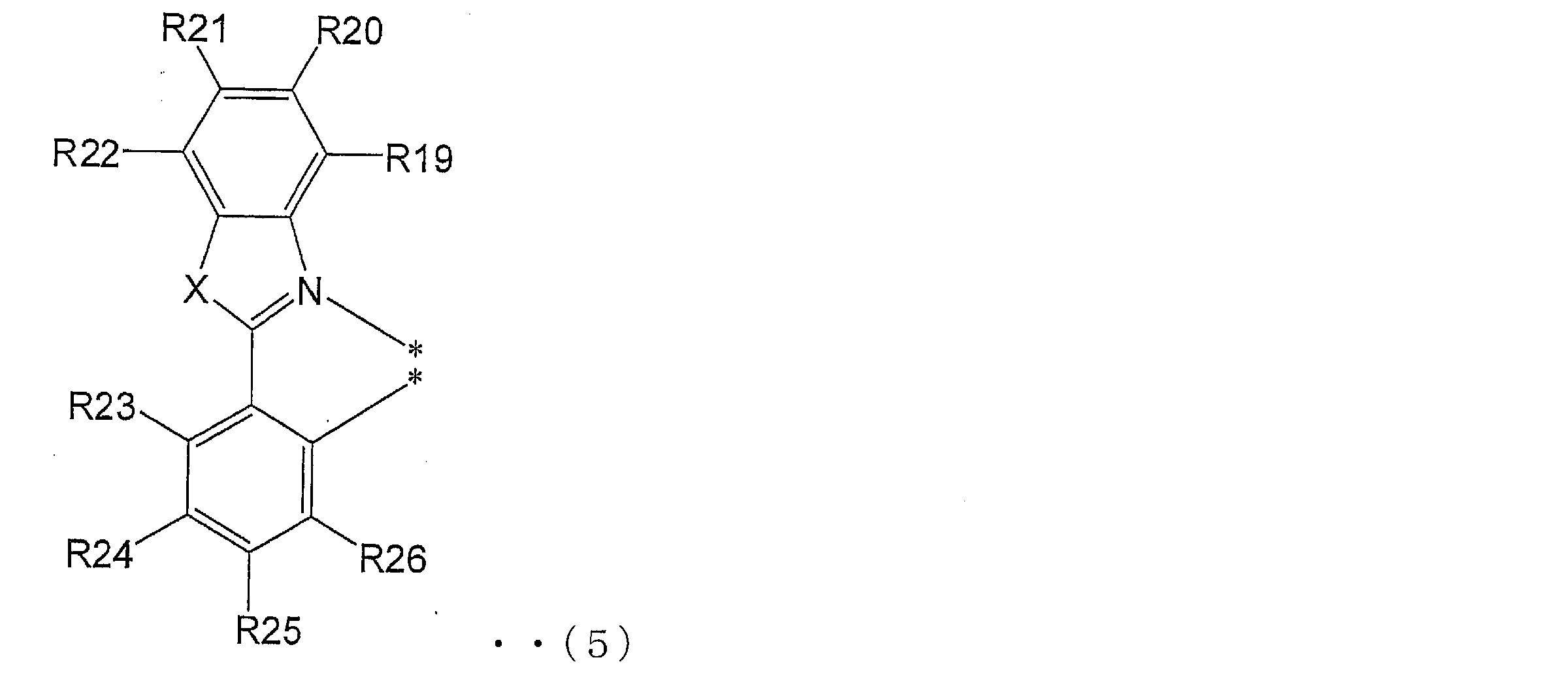
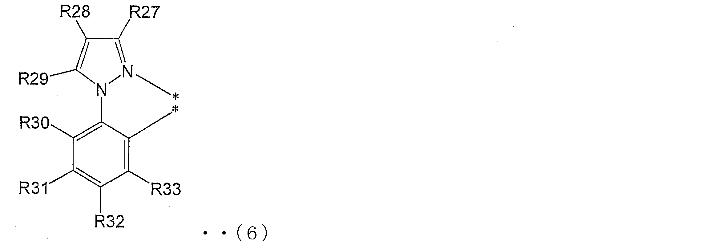
- 上記一般式(1)中で、Mがイリジウム、オスミウム又は白金を表すことを特徴とする請求項1~3の何れか一項に記載の錯体化合物。
- 請求項1~4の何れか一項に記載の錯体化合物に電圧を印加して、当該錯体化合物を発光させることを特徴とする発光方法。
- 一対の電極と、該一対の電極間に配された発光材料を含む発光層とを含んでなる発光素子であって、
上記発光層が請求項1~4の何れか一項に記載の錯体化合物を含んでなることを特徴とする発光素子。
Applications Claiming Priority (2)
| Application Number | Priority Date | Filing Date | Title |
|---|---|---|---|
| JP2011-038483 | 2011-02-24 | ||
| JP2011038483 | 2011-02-24 |
Publications (1)
| Publication Number | Publication Date |
|---|---|
| WO2012114940A1 true WO2012114940A1 (ja) | 2012-08-30 |
Family
ID=46720722
Family Applications (1)
| Application Number | Title | Priority Date | Filing Date |
|---|---|---|---|
| PCT/JP2012/053392 Ceased WO2012114940A1 (ja) | 2011-02-24 | 2012-02-14 | 新規錯体化合物、及びその利用 |
Country Status (1)
| Country | Link |
|---|---|
| WO (1) | WO2012114940A1 (ja) |
Citations (4)
| Publication number | Priority date | Publication date | Assignee | Title |
|---|---|---|---|---|
| JP2005298483A (ja) * | 2004-03-17 | 2005-10-27 | National Institute Of Advanced Industrial & Technology | イリジウム錯体およびこれを用いた発光材料 |
| WO2005118606A1 (ja) * | 2004-06-04 | 2005-12-15 | National Institute Of Advanced Industrial Science And Technology | フッ素置換イリジウム錯体およびこれを用いた発光材料 |
| JP2007217364A (ja) * | 2006-02-17 | 2007-08-30 | National Institute Of Advanced Industrial & Technology | 新規金属錯体およびこれを用いた発光材料 |
| JP2008303205A (ja) * | 2007-05-10 | 2008-12-18 | National Institute Of Advanced Industrial & Technology | 金属配位化合物ならびにこれを用いた発光材料 |
-
2012
- 2012-02-14 WO PCT/JP2012/053392 patent/WO2012114940A1/ja not_active Ceased
Patent Citations (4)
| Publication number | Priority date | Publication date | Assignee | Title |
|---|---|---|---|---|
| JP2005298483A (ja) * | 2004-03-17 | 2005-10-27 | National Institute Of Advanced Industrial & Technology | イリジウム錯体およびこれを用いた発光材料 |
| WO2005118606A1 (ja) * | 2004-06-04 | 2005-12-15 | National Institute Of Advanced Industrial Science And Technology | フッ素置換イリジウム錯体およびこれを用いた発光材料 |
| JP2007217364A (ja) * | 2006-02-17 | 2007-08-30 | National Institute Of Advanced Industrial & Technology | 新規金属錯体およびこれを用いた発光材料 |
| JP2008303205A (ja) * | 2007-05-10 | 2008-12-18 | National Institute Of Advanced Industrial & Technology | 金属配位化合物ならびにこれを用いた発光材料 |
Similar Documents
| Publication | Publication Date | Title |
|---|---|---|
| JP5549015B2 (ja) | 新規化合物、及びその利用 | |
| JP5466005B2 (ja) | Oledアプリケーション用オキサゾール−三重項−発光体 | |
| Xu et al. | Synthesis and properties of iridium complexes based 1, 3, 4-oxadiazoles derivatives | |
| Zhang et al. | Solution-processed blue–green organic light-emitting diodes based on cationic iridium complexes with 1-pyridyl-3-methylimidazolin-2-ylidene-C, C2′ as the ancillary ligand | |
| US20040121184A1 (en) | Organic light emitting materials and devices | |
| Ding et al. | Highly efficient phosphorescent bis-cyclometalated iridium complexes based on quinoline ligands | |
| EP2007780B1 (en) | Light-emitting material | |
| Ge et al. | Highly efficient phosphorescent iridium (III) diazine complexes for OLEDs: Different photophysical property between iridium (III) pyrazine complex and iridium (III) pyrimidine complex | |
| JP2012517492A (ja) | Oledの発光層中のホストドーパントとして使用される発光材料 | |
| Rai et al. | Guanidinate ligated iridium (III) complexes with various cyclometalated ligands: synthesis, structure, and highly efficient electrophosphorescent properties with a wide range of emission colours | |
| Zhang et al. | Photo-and electro-luminescence of four cuprous complexes with sterically demanding and hole transmitting diimine ligands | |
| US20110012093A1 (en) | Luminescent gold(iii) compounds containing bidentate ligand for organic light-emitting devices and their preparation | |
| Rai et al. | Substituent effect on the electroluminescence efficiency of amidinate-ligated bis (pyridylphenyl) iridium (III) complexes | |
| Yun et al. | Homoleptic cyclometalated dibenzothiophene–NHC–iridium (iii) complexes for efficient blue phosphorescent organic light-emitting diodes | |
| Orwat et al. | Microwave-assisted one-pot synthesis of new ionic iridium complexes of [Ir (bzq) 2 (N^ N)]+ A− type and their selected electroluminescent properties | |
| KR20120038319A (ko) | 유기전계발광소자의 인광재료용 백금 착체 | |
| US20100174078A1 (en) | Bipyridine metal complexes for use as light-emitting material | |
| EP2496590A1 (en) | Ion-pairing soft salts based on organometallic complexes and their applications in organic light emitting diodes | |
| US10461266B2 (en) | Luminescent compounds and methods of using same | |
| Lu et al. | Efficient electroluminescence of platinum complexes containing pinene sterically hindered spacer | |
| WO2007042474A2 (en) | Light-emitting material | |
| WO2008043815A1 (en) | Light-emitting material | |
| Mitsumori et al. | Synthesis, properties, and LED performance of highly luminescent metal complexes containing indolizino [3, 4, 5-ab] isoindoles | |
| Yang et al. | Bathochromic effect of trifluoromethyl-substituted 2-naphthalen-1-yl-pyridine ligands in color tuning of iridium complexes | |
| US8357799B2 (en) | Light emitting material |
Legal Events
| Date | Code | Title | Description |
|---|---|---|---|
| 121 | Ep: the epo has been informed by wipo that ep was designated in this application |
Ref document number: 12749608 Country of ref document: EP Kind code of ref document: A1 |
|
| NENP | Non-entry into the national phase |
Ref country code: DE |
|
| 122 | Ep: pct application non-entry in european phase |
Ref document number: 12749608 Country of ref document: EP Kind code of ref document: A1 |
|
| NENP | Non-entry into the national phase |
Ref country code: JP |