WO2012114911A1 - 液晶表示装置および光源装置 - Google Patents
液晶表示装置および光源装置 Download PDFInfo
- Publication number
- WO2012114911A1 WO2012114911A1 PCT/JP2012/053142 JP2012053142W WO2012114911A1 WO 2012114911 A1 WO2012114911 A1 WO 2012114911A1 JP 2012053142 W JP2012053142 W JP 2012053142W WO 2012114911 A1 WO2012114911 A1 WO 2012114911A1
- Authority
- WO
- WIPO (PCT)
- Prior art keywords
- light
- liquid crystal
- display device
- light guide
- crystal display
- Prior art date
- Legal status (The legal status is an assumption and is not a legal conclusion. Google has not performed a legal analysis and makes no representation as to the accuracy of the status listed.)
- Ceased
Links
Images





Classifications
-
- G—PHYSICS
- G02—OPTICS
- G02B—OPTICAL ELEMENTS, SYSTEMS OR APPARATUS
- G02B6/00—Light guides; Structural details of arrangements comprising light guides and other optical elements, e.g. couplings
- G02B6/0001—Light guides; Structural details of arrangements comprising light guides and other optical elements, e.g. couplings specially adapted for lighting devices or systems
- G02B6/0011—Light guides; Structural details of arrangements comprising light guides and other optical elements, e.g. couplings specially adapted for lighting devices or systems the light guides being planar or of plate-like form
- G02B6/0033—Means for improving the coupling-out of light from the light guide
- G02B6/0056—Means for improving the coupling-out of light from the light guide for producing polarisation effects, e.g. by a surface with polarizing properties or by an additional polarizing elements
-
- G—PHYSICS
- G02—OPTICS
- G02F—OPTICAL DEVICES OR ARRANGEMENTS FOR THE CONTROL OF LIGHT BY MODIFICATION OF THE OPTICAL PROPERTIES OF THE MEDIA OF THE ELEMENTS INVOLVED THEREIN; NON-LINEAR OPTICS; FREQUENCY-CHANGING OF LIGHT; OPTICAL LOGIC ELEMENTS; OPTICAL ANALOGUE/DIGITAL CONVERTERS
- G02F1/00—Devices or arrangements for the control of the intensity, colour, phase, polarisation or direction of light arriving from an independent light source, e.g. switching, gating or modulating; Non-linear optics
- G02F1/01—Devices or arrangements for the control of the intensity, colour, phase, polarisation or direction of light arriving from an independent light source, e.g. switching, gating or modulating; Non-linear optics for the control of the intensity, phase, polarisation or colour
- G02F1/13—Devices or arrangements for the control of the intensity, colour, phase, polarisation or direction of light arriving from an independent light source, e.g. switching, gating or modulating; Non-linear optics for the control of the intensity, phase, polarisation or colour based on liquid crystals, e.g. single liquid crystal display cells
- G02F1/133—Constructional arrangements; Operation of liquid crystal cells; Circuit arrangements
- G02F1/1333—Constructional arrangements; Manufacturing methods
- G02F1/1335—Structural association of cells with optical devices, e.g. polarisers or reflectors
- G02F1/1336—Illuminating devices
- G02F1/133615—Edge-illuminating devices, i.e. illuminating from the side
-
- G—PHYSICS
- G02—OPTICS
- G02B—OPTICAL ELEMENTS, SYSTEMS OR APPARATUS
- G02B6/00—Light guides; Structural details of arrangements comprising light guides and other optical elements, e.g. couplings
- G02B6/0001—Light guides; Structural details of arrangements comprising light guides and other optical elements, e.g. couplings specially adapted for lighting devices or systems
- G02B6/0011—Light guides; Structural details of arrangements comprising light guides and other optical elements, e.g. couplings specially adapted for lighting devices or systems the light guides being planar or of plate-like form
- G02B6/0033—Means for improving the coupling-out of light from the light guide
- G02B6/0035—Means for improving the coupling-out of light from the light guide provided on the surface of the light guide or in the bulk of it
- G02B6/0038—Linear indentations or grooves, e.g. arc-shaped grooves or meandering grooves, extending over the full length or width of the light guide
Definitions
- the present invention relates to a liquid crystal display device and a light source device.
- This application claims priority based on Japanese Patent Application No. 2011-038385 filed in Japan on February 24, 2011, the contents of which are incorporated herein by reference.
- Liquid crystal display devices are widely used as portable electronic devices such as cellular phones or displays for televisions, personal computers, and the like.
- display is performed using light emitted from a surface-emitting light source disposed on the back side of a liquid crystal cell.
- this type of surface-emitting light source may be referred to as a backlight.
- Patent Document 1 listed below discloses a surface light emitting device that includes a polarized light source that emits polarized light, and a light guide plate made of a light-transmitting resin having a low birefringence whose retardation is 1 ⁇ 4 or less of the wavelength of the polarized light. Has been. Further, Patent Document 1 discloses a liquid crystal display device including the above-described surface light emitting device, a polarizing plate as a polarizer, a liquid crystal cell, and a polarizing plate as an analyzer.
- One embodiment of the present invention has been made to solve at least one of the above problems, and an object thereof is to provide a liquid crystal display device capable of reducing manufacturing cost or improving display contrast. It is another object of the present invention to provide a light source device suitable for use in this type of liquid crystal display device.
- a liquid crystal display device includes a light source device, a first polarizing plate, a liquid crystal cell that is provided between the light source device and the first polarizing plate, and modulates light emitted from the light source device.
- the light source device emits polarized light having a polarization axis, an end face on which the polarized light incident from the light emitting unit is incident, a reflective surface that reflects the polarized light, and the reflected polarized light is emitted.
- a light guide made of a light transmissive material having low birefringence, and the polarization axis of the polarized light incident on the light guide from the light emitting portion is the guide.
- the light emitting part is arranged with respect to the light guide part so as to be substantially parallel or substantially perpendicular to the light exit surface of the light body.
- the first polarizing plate may be provided only on the light emission side of the liquid crystal cell.
- the liquid crystal cell may include a liquid crystal layer, and the liquid crystal cell may include a second polarizing plate between the liquid crystal layer and the light source device.
- the light guide has an uneven structure
- the reflective surface is an inclined surface of the uneven structure
- the extending direction of the uneven structure is from the light emitting element. It may be substantially orthogonal to the direction of travel of the emitted polarized light.
- the light-emitting element forming the light-emitting portion may be formed of a group III nitride semiconductor material having a nonpolar surface or a semipolar surface as a main surface.
- the light guide is a mixture of a positive birefringent material and a negative birefringent material, or a copolymer of a positive birefringent material and a negative birefringent material. It may be constituted by.
- a light source device includes a light emitting unit that emits polarized light having a polarization axis, an end surface on which polarized light incident from the light emitting unit is incident, a reflective surface that reflects the polarized light, and the reflected polarized light. And a light guide made of a light transmissive material having low birefringence, and the polarization axis of the polarized light incident on the light guide from the light emitting unit is The light emitting part is arranged with respect to the light guide part so as to be substantially parallel or substantially perpendicular to the light exit surface of the light guide.
- liquid crystal display device capable of reducing manufacturing costs or improving display contrast.
- a light source device suitable for use in this type of liquid crystal display device can be provided.
- FIG. 1 is a perspective view showing a liquid crystal display device of the present embodiment.
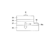
- FIG. 2 is a cross-sectional view showing an LED used in the light source device of the present embodiment.
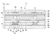
- FIG. 3 is a cross-sectional view showing a portion of the liquid crystal cell of the liquid crystal display device of the present embodiment.
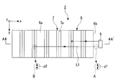
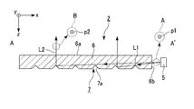
- 4A and 4B are diagrams for explaining the operation of the backlight of the present embodiment.
- FIG. 4A is a plan view seen from the normal direction of the xy plane.
- FIG. 4B is a cross-sectional view taken along the xz plane.
- the scale of the size may be changed depending on the component.
- the x-axis is the horizontal direction of the screen of the liquid crystal display device (the extending direction of the scanning lines)
- the y-axis is the vertical direction of the screen of the liquid crystal display device (the direction perpendicular to the extending direction of the scanning lines)
- the z-axis Is defined as the thickness direction of the liquid crystal display device.
- the liquid crystal display device 1 of this embodiment includes a backlight 2 (light source device), a liquid crystal cell 3, and a polarizing plate 4, as shown in FIG.
- the backlight 2 includes a light emitting diode (Light Emitting Diode, hereinafter abbreviated as LED) 5 and a light guide 6.
- the LED 5 (light emitting unit) of the present embodiment emits polarized light having a predetermined polarization axis.
- the light guide 6 is made of a light transmissive material having low birefringence. The configuration of the LED 5 and the light guide 6 will be described in detail later.
- the liquid crystal cell 3 is schematically illustrated as a single plate, but the detailed structure thereof will be described later.
- liquid crystal display device 1 of the present embodiment light emitted from the backlight 2 is modulated by the liquid crystal cell 3, and a predetermined image, characters, or the like is displayed by the modulated light.
- the observer sees images and characters from above the liquid crystal display device 1 in FIG. Therefore, in the following description, the side on which the polarizing plate 4 is disposed is referred to as a viewing side, and the side on which the backlight 2 is disposed is referred to as a back side.
- the light guide body 6 of the present embodiment has a plate shape, and has two main surfaces and four end surfaces.
- the upper main surface 6a shown in FIG. 1 is a surface from which the light L2 is emitted.
- the LED 5 is disposed on one end surface 6b of the four end surfaces of the light guide 6, and the light L1 enters from the end surface 6b of the light guide 6 on which the LED 5 is disposed.
- the lower main surface 6 c shown in FIG. 1 has a plurality of grooves 7 (concavo-convex structure) having a triangular cross-sectional shape along the xz plane, as shown in FIGS.
- each groove 7 is substantially parallel to the y-axis direction, and the plurality of grooves 7 are provided substantially parallel to each other.
- the surface 7a facing the traveling direction of the light L1 from the LED 5 functions as a reflecting surface. Therefore, the light incident from the end surface 6b of the light guide 6 is reflected by the reflecting surface 7a, changes its traveling direction, and is emitted from the main surface 6a.
- the main surface 6 a from which light is emitted is referred to as a “light emission surface”.
- the end face 6 b on which light is incident is referred to as a “light incident end face”.
- the LED 5 of the present embodiment emits polarized light.
- “Polarized light” is light whose vibration direction is biased in a specific direction. However, in the case of this embodiment, it is not always necessary that all polarized components have a vibration direction aligned in one direction. That is, there is no need for 100% linearly polarized light. Therefore, the polarization axis of light is defined as the vibration direction of the linearly polarized light component that is contained most in the light.
- the LED 5 includes a semiconductor substrate 36, a first conductivity type first semiconductor layer 37, an active layer 38, and a second conductivity type second semiconductor layer 39 sequentially stacked thereon. is doing.
- the semiconductor substrate 36 is made of a GaN single crystal, and its main surface 36a is composed of a non-polar plane (Non-polar Plane) or a semipolar plane (Semi-polar Plane) of the GaN crystal.
- the first semiconductor layer 37, the active layer 38, and the second semiconductor layer 39 are obtained by using the main surface 36a of the semiconductor substrate 36 as a crystal growth surface and crystal-growing a semiconductor material thereon.
- the LED 5 is made of a group III nitride semiconductor such as aluminum nitride (AlN), gallium nitride (GaN), or indium nitride (InN) whose main surface is the m-plane. Composed.
- a typical group III nitride semiconductor is represented by Al x In y Ga 1-xy N (0 ⁇ x ⁇ 1, 0 ⁇ y ⁇ 1, 0 ⁇ x + y ⁇ 1).
- a GaN semiconductor is a group III-V compound semiconductor well known among hexagonal compound semiconductors containing nitrogen.
- the active layer 38 is supplied with carriers of the first conductivity type from the first semiconductor layer 37 and is supplied with carriers of the second conductivity type from the second semiconductor layer 39.
- the first conductivity type is n-type and the second conductivity type is p-type
- electrons supplied from the first semiconductor layer 37 and holes supplied from the second semiconductor layer 39 are regenerated in the active layer 38.
- the light L1 is emitted from the active layer 38.
- a quantum well (Quantum Well) structure in which a well layer is sandwiched between barrier layers having a band gap larger than that of the well layer, or a multiple quantum well (MQW) structure can be employed.
- the active layer is a group III nitride semiconductor having a GaN crystal polar face as the crystal growth surface, light in a randomly polarized (non-polarized) state is emitted from the active layer.
- polarized light L1 is generated from the active layer 38 formed using a group III nitride semiconductor having a nonpolar plane or a semipolar plane as a crystal growth surface.
- the LED 5 includes a first electrode 40 that supplies an operating voltage to the first semiconductor layer 37 and a second electrode 41 that supplies an operating voltage to the second semiconductor layer 39.
- a first electrode 40 is formed on the surface of the second semiconductor layer 39, the active layer 38, and the first semiconductor layer 37 that is partially removed in the thickness direction and the first semiconductor layer 37 is exposed.
- aluminum (Al) is used as the material of the first electrode 40.
- a palladium (Pd) -gold (Au) alloy is used as the material of the second electrode 41.
- the first electrode 40 is ohmically connected to the first semiconductor layer 37, and the second electrode 41 is ohmically connected to the second semiconductor layer 39.
- a first conductivity type contact layer may be interposed between the first semiconductor layer 37 and the first electrode 40.
- a second conductivity type contact layer may be interposed between the second semiconductor layer 39 and the second electrode 41.
- the LED 5 and the light guide 6 are fixed so that the back surface of the semiconductor substrate 36 constituting the LED 5 faces the light incident end surface 6 b of the light guide 6.
- LED5 with high directivity by which the emission direction of the light L1 was controlled to substantially one direction is used.
- the light guide 6 is made of a light transmissive resin material having low birefringence.
- “low birefringence” means that the retardation that the light receives in the optical path from when the light L1 enters the light guide 6 until it is emitted is equal to or less than 1 ⁇ 4 of the wavelength of the light.
- the resin material having low birefringence whose retardation is 1 ⁇ 4 or less of the wavelength of light is a mixture of a positive birefringent substance and a negative birefringent substance, or positive birefringence. It is composed of a copolymer of a substance and a negative birefringent substance.
- the positive birefringent material for example, a material selected from polyvinylidene fluoride (PVDF), polyvinylidene fluoride trifluoroethylene (VDF ⁇ TrFE-58), polyethylene oxide (PEO) and the like may be used. Although preferable, it is not limited to these.
- the negative birefringent material is preferably, for example, polymethyl methacrylate (PMMA), but is not limited thereto. Note that the positive birefringent material and the negative birefringent material may be one type of the plurality of materials listed above, or a combination of a plurality of types.
- a low birefringent material having retardation of 1 ⁇ 4 or less of the wavelength of light can be used in which a low molecular organic substance having a rod-like molecular shape and anisotropy in polarizability is added to a polymer.
- a low molecular organic substance having a rod-like molecular shape and anisotropy in polarizability is added to a polymer.
- the inorganic birefringent crystal fine particle to the polymer can also be used.
- liquid crystal cell 3 an active matrix transmissive liquid crystal cell will be described as an example, but a liquid crystal cell applicable to the present embodiment is not limited to an active matrix transmissive liquid crystal cell.
- the liquid crystal cell applicable to the present embodiment may be, for example, a transflective (transmissive and reflective) liquid crystal cell or a reflective liquid crystal cell, and each pixel is a switching thin film transistor (Thin Film Transistor, hereinafter).
- Thin Film Transistor hereinafter
- a simple matrix type liquid crystal cell not provided with TFT may be used to the liquid crystal cell.
- FIG. 3 is a longitudinal sectional view of the liquid crystal cell 3.
- the liquid crystal cell 3 includes a TFT substrate 9 as a switching element substrate, a color filter substrate 10 disposed opposite to the TFT substrate 9, and the TFT substrate 9 and the color filter substrate 10. And a sandwiched liquid crystal layer 11.
- the liquid crystal layer 11 is surrounded by a TFT substrate 9, a color filter substrate 10, and a frame-shaped seal member (not shown) that bonds the TFT substrate 9 and the color filter substrate 10 at a predetermined interval. It is enclosed in the space.
- the liquid crystal cell 3 of the present embodiment performs display in, for example, a VA (Vertical Alignment, vertical alignment) mode, and a vertical alignment liquid crystal having a negative dielectric anisotropy is used for the liquid crystal layer 11.
- a spherical spacer 12 is disposed between the TFT substrate 9 and the color filter substrate 10 to keep the distance between these substrates constant.
- the display mode is not limited to the VA mode described above, and a TN (Twisted Nematic) mode, a STN (Super Twisted Nematic) mode, an IPS (In-Plane Switching) mode, or the like can be used.
- the TFT substrate 9 has a plurality of pixels (not shown) as a minimum unit area for display arranged in a matrix.
- a plurality of source bus lines (not shown) are formed on the TFT substrate 9 so as to extend substantially parallel to each other, and a plurality of gate bus lines (not shown) extend substantially parallel to each other. And formed so as to be orthogonal to the plurality of source bus lines. Therefore, on the TFT substrate 9, a plurality of source bus lines and a plurality of gate bus lines are formed in a lattice pattern, and a rectangular region partitioned by adjacent source bus lines and adjacent gate bus lines is one. One pixel.
- the source bus line is connected to the source electrode of the TFT described later, and the gate bus line is connected to the gate electrode of the TFT.
- a TFT 19 having a semiconductor layer 15, a gate electrode 16, a source electrode 17, a drain electrode 18, and the like is formed on the surface of the transparent substrate 14 constituting the TFT substrate 9 on the liquid crystal layer 11 side.
- a transparent substrate 14 for example, a glass substrate can be used.
- a semiconductor material such as CGS (Continuous Grain Silicon: continuous grain boundary silicon), LPS (Low-temperature Poly-Silicon: low-temperature polycrystalline silicon), ⁇ -Si (Amorphous Silicon: amorphous silicon), or the like.
- a semiconductor layer 15 is formed.
- a gate insulating film 20 is formed on the transparent substrate 14 so as to cover the semiconductor layer 15.
- the gate insulating film 20 As a material of the gate insulating film 20, for example, a silicon oxide film, a silicon nitride film, or a laminated film thereof is used. A gate electrode 16 is formed on the gate insulating film 20 so as to face the semiconductor layer 15. As the material of the gate electrode 16, for example, a laminated film of W (tungsten) / TaN (tantalum nitride), Mo (molybdenum), Ti (titanium), Al (aluminum), or the like is used.
- a first interlayer insulating film 21 is formed on the gate insulating film 20 so as to cover the gate electrode 16.
- a material of the first interlayer insulating film 21 for example, a silicon oxide film, a silicon nitride film, or a laminated film thereof is used.
- a source electrode 17 and a drain electrode 18 are formed on the first interlayer insulating film 21.
- the source electrode 17 is connected to the source region of the semiconductor layer 15 through a contact hole 22 that penetrates the first interlayer insulating film 21 and the gate insulating film 20.
- the drain electrode 18 is connected to the drain region of the semiconductor layer 15 through a contact hole 23 that penetrates the first interlayer insulating film 21 and the gate insulating film 20.
- the same conductive material as that for the gate electrode 16 is used.
- a second interlayer insulating film 24 is formed on the first interlayer insulating film 21 so as to cover the source electrode 17 and the drain electrode 18.
- the same material as the first interlayer insulating film 21 described above or an organic insulating material is used.
- a pixel electrode 25 is formed on the second interlayer insulating film 24.
- the pixel electrode 25 is connected to the drain electrode 18 through a contact hole 26 that penetrates the second interlayer insulating film 24. Therefore, the pixel electrode 25 is connected to the drain region of the semiconductor layer 15 using the drain electrode 18 as a relay electrode.
- a transparent conductive material such as ITO (Indium Tin Oxide, Indium Tin Oxide) or IZO (Indium Zinc Oxide, Indium Zinc Oxide) is used.
- An alignment film 27 is formed on the second interlayer insulating film 24 so as to cover the pixel electrode 25.
- This alignment film 27 has an alignment regulating force for vertically aligning liquid crystal molecules constituting the liquid crystal layer 11.
- the form of the TFT may be the bottom gate TFT shown in FIG. 3 or the top gate TFT.
- a black matrix 30, a color filter 31, a planarizing layer 32, a counter electrode 33, and an alignment film 34 are sequentially formed on the surface of the transparent substrate 29 constituting the color filter substrate 10 on the liquid crystal layer 11 side.
- the black matrix 30 has a function of blocking light transmission in the inter-pixel region.
- the black matrix 30 is formed of a metal such as Cr (chromium) or a Cr / Cr oxide multilayer film, or a photoresist in which carbon particles are dispersed in a photosensitive resin.
- the color filter 31 includes dyes of red (R), green (G), and blue (B), and one pixel electrode 25 on the TFT substrate 9 is any one of R, G, and B. Two color filters 31 are arranged to face each other.
- the flattening layer 32 is made of an insulating film that covers the black matrix 30 and the color filter 31, and has a function of smoothing and flattening a step formed by the black matrix 30 and the color filter 31.
- a counter electrode 33 is formed on the planarization layer 32. As the material of the counter electrode 33, a transparent conductive material similar to that of the pixel electrode 25 is used. Further, an alignment film 34 having a vertical alignment regulating force is formed on the entire surface of the counter electrode 33.
- the color filter 31 may have a multicolor configuration of three or more colors of R, G, and B.
- a polarizing plate 4 for regulating transmission / blocking of light modulated by the liquid crystal cell 3 is provided on the viewing side of the liquid crystal cell 3. Yes.
- the liquid crystal cell 3 and the polarizing plate 4 are drawn apart from each other, but actually, the polarizing plate 4 is bonded to one surface of the color filter substrate 10 constituting the liquid crystal cell 3 via an adhesive layer or the like. Also good.
- a polarizing plate for regulating the polarization axis of light incident on the liquid crystal cell 3 is not provided between the backlight 2 and the liquid crystal cell 3.
- the polarization axis of the light L1 incident on the light guide 6 from the LED 5 is relative to the light exit surface 6a (xy plane) of the light guide 6.
- the direction of the LED 5 with respect to the light guide 6 is set so as to be substantially parallel and disposed substantially parallel (y-axis direction) to the light incident end face 6b.
- the polarization direction p1 of the light L1 at this time is shown in a circle indicated by symbol A in FIGS. 4A and 4B.
- the LED 5 with high directivity is used, the light L1 travels in a direction (x-axis direction) substantially perpendicular to the light incident end surface 6b inside the light guide 6.
- the polarization axis direction of the light L1 is substantially the direction at the time of incidence while the light L1 travels inside the light guide 6. It remains maintained at p1. 4A and 4B, the LED 5 and the light guide plate 6 are drawn apart for convenience of explanation.
- the groove 7 (reflecting surface 7a) of the light guide 6 extends in a direction (y-axis direction) substantially parallel to the extending direction of the light incident end face 6b, the light L1 traveling inside the light guide 6 is obtained. Is incident on the reflecting surface 7a from the direction substantially perpendicular to the extending direction of the reflecting surface 7a (x-axis direction) and is reflected. In the case of a light guide that scatters light using a scattering material or the like and emits the light to the outside, the direction of the polarization axis of the light is disturbed by the scattering, and the direction of the polarization axis is not maintained.
- the direction of the polarization axis of the reflected light L2 is the same as that before the reflection. Therefore, the polarization axis of the light L2 emitted from the light emitting surface 6a to the outside after being reflected by the reflecting surface 7a and changing the traveling direction is substantially parallel to the light emitting surface 6a of the light guide 6 and the light. A direction substantially parallel to the incident end face 6b is maintained.
- the polarization direction p2 of the light L2 at this time is shown in a circle indicated by a symbol B in FIGS. 4A and 4B.
- the polarization axis direction p2 of the light L2 incident on the liquid crystal cell 3 from the backlight 2 is the y-axis direction
- the viewing axis direction p4 of the viewing-side polarizing plate 4 is the x-axis direction. That is, the direction p2 of the polarization axis of the light L2 incident on the liquid crystal cell 3 and the transmission axis direction p4 of the polarizing plate 4 are arranged to be orthogonal to each other.
- the polarizing plate 4 is rotated 90 degrees in the xy plane from the state shown in FIG. 1 so that the polarization axis direction p2 of the light L2 incident on the liquid crystal cell 3 and the transmission axis direction p4 of the polarizing plate 4 are substantially parallel. Can be displayed in the normally white mode.
- the polarized light whose polarization axes are substantially aligned in one direction is emitted from the backlight 2, between the backlight and the liquid crystal cell used in the conventional general liquid crystal display device.
- the polarizing plate can be eliminated.
- the material cost can be reduced by reducing the number of parts, the manufacturing cost required for attaching the polarizing plate can be reduced, and the cost of the entire liquid crystal display device can be reduced.
- LED5 which consists of a group III nitride semiconductor material which makes a nonpolar surface or a semipolar surface a main surface, and emits linearly polarized light directly was used.
- a polarizing plate may be attached to a light emitting surface of an LED that emits light with a random polarization state, and an LED that emits linearly polarized light by emitting light through the polarizing plate may be used.
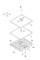
- FIG. 5 is a perspective view showing the liquid crystal display device of the present embodiment.
- 6A and 6B are diagrams for explaining the operation of the backlight of the present embodiment.
- FIG. 6A is a plan view seen from the normal direction of the xy plane.
- FIG. 6B is a cross-sectional view taken along the xz plane. 5 to 6B, the same components as those in FIGS. 1, 4A, and 4B used in the first embodiment are denoted by the same reference numerals, and detailed description thereof is omitted.
- the polarizing plate 4 is provided on the viewing side of the liquid crystal cell 3, and between the backlight 44 and the liquid crystal cell 3. Is not provided with a polarizing plate.
- the transmission axis direction p4 of the polarizing plate 4 on the viewing side of the liquid crystal cell 3 is set in the y-axis direction.
- the polarization axis p1 of the light L1 incident on the light guide 6 from the LED 5 is on the light exit surface 6a (xy plane) of the light guide 6.
- the direction of the LED 5 with respect to the light guide 6 is set so as to be arranged vertically (z-axis direction).
- the polarization direction p1 of the light L1 at this time is shown in a circle with a symbol A in FIGS. 6A and 6B.
- the light L1 travels in a direction (x-axis direction) substantially perpendicular to the light incident end surface 6b inside the light guide 6.
- the polarization axis direction of the light L1 is substantially the direction at the time of incidence while the light L1 travels inside the light guide 6. It remains maintained at p1.
- the groove 7 (reflecting surface 7a) of the light guide 6 extends in a direction (y-axis direction) substantially parallel to the extending direction of the light incident end face 6b, the light L1 traveling inside the light guide 6 is obtained. Is incident on the reflecting surface 7a from the direction substantially perpendicular to the extending direction of the reflecting surface 7a (x-axis direction) and is reflected.
- the direction p2 of the polarization axis of the light L2 after being reflected by the reflecting surface 7a is the same as that before reflection when viewed from the optical axis side of the light L2.
- the traveling direction of the light changes by approximately 90 degrees
- the direction p2 of the polarization axis of the light L2 when viewed from the outside rotates approximately 90 degrees with respect to the direction p1 of the polarization axis at the time of incidence and becomes the x-axis direction.
- the polarization direction p2 of the light L2 at this time is shown in a circle indicated by B in FIGS. 6A and 6B.
- FIG. 7 is a perspective view showing the liquid crystal display device of the present embodiment.
- FIG. 8 is a cross-sectional view of the liquid crystal cell of this embodiment.
- symbol is attached
- the polarizing plate 4 is provided on the viewing side of the liquid crystal cell 47, and the backlight 2, the liquid crystal cell 47, A polarizing plate is not provided between them.
- the transmission axis direction of the polarizing plate 4 on the viewing side of the liquid crystal cell 47 is set in the x-axis direction.
- the liquid crystal cell 47 has a polarizing plate 48 formed on the surface of the transparent substrate 14 constituting the TFT substrate 9 on the liquid crystal layer 11 side.
- the polarizing plate 48 is formed by directly forming a wire grid made of a large number of fine metal wires formed at intervals of about the wavelength of light or a layer of a dichroic dye on the transparent substrate 14.
- This polarizing plate 48 is formed in the liquid crystal cell 47, and in order to distinguish it from the polarizing plate 4 outside the liquid crystal cell, it will be referred to as “in-cell polarizing plate” in the following description.
- the liquid crystal cell 47 of this embodiment is the same as the liquid crystal cell 3 of the first embodiment shown in FIG.
- the transmission axis direction of the intra-cell polarizing plate 48 is set to a direction p3 (y-axis direction) substantially parallel to the polarization axis direction p1 of the light L1 emitted from the LED 5, as shown in FIG.
- the material cost can be reduced by reducing the number of parts, the manufacturing cost required for the polarizing plate attaching operation can be reduced, and the overall cost of the liquid crystal display device can be reduced. The same effect as in the second embodiment can be obtained.
- the backlight 2 of the present embodiment uses a light transmissive material having low birefringence as the material of the light guide 6. Therefore, basically, when the light L1 travels in the light guide 6, the polarization axis direction of the light is maintained in the incident direction p1. However, since the light guide 6 has a slight birefringence, a slightly polarized component having a polarization axis in a direction different from the polarization axis direction p1 of the incident light is generated. As a result, as shown in FIG.
- the light L2 emitted from the backlight 2 has a polarization axis direction p2 substantially parallel to the polarization axis direction p1 of the light L1 emitted from the LED 5, and the other polarization axis directions p2 ′. It becomes light that is mixed. When display is performed using such light L2, the contrast of the display is lowered.
- the in-cell polarizing plate 48 is provided in the liquid crystal cell 47 of the present embodiment, the polarization axis direction p2 ′ in a direction different from the polarization axis direction p1 of the light L1 when entering the light guide 6 is set.
- the polarization component possessed is absorbed or reflected by the in-cell polarizing plate 48. Therefore, at the time when light is incident on the liquid crystal layer 11 in the liquid crystal cell 47, the directions of the polarization axes of the light are substantially aligned.
- the liquid crystal display device 46 of this embodiment in addition to the effect of cost reduction, the effect that the contrast of a display can be improved can be acquired.
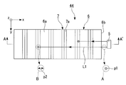
- FIG. 9 is a plan view showing the backlight of the present embodiment.
- FIG. 10 is a plan view showing another example of the backlight of the present embodiment. 9 and 10, the same reference numerals are given to the same components as those in FIG. 4A used in the first embodiment, and detailed description thereof will be omitted.
- the backlight 50 of the present embodiment includes a light emitting unit 54 including a LED 51, a first light guide 52 and a polarizing plate 53, and a second light guide 55.
- the LED 51 emits light having a polarization axis in a random direction.
- the first light guide 52 is constituted by a prism structure having a longitudinal dimension substantially the same as the dimension of the light incident end face 55 b of the second light guide 55.
- the planar shape of the first light guide 52 viewed from the normal direction of the xy plane is a right triangle, two surfaces orthogonal to each other are the installation surface 52b and the light emission surface 52a of the LED 51, and the inclined surface is the light from the LED.
- the second light guide 55 is provided with a plurality of prism structures 56 on the light incident end face of the light guide 6 as in the first embodiment.
- a polarizing plate 53 is provided between the light exit surface 52 a of the first light guide 52 and the prism structure 56 of the second light guide 55.
- the light emitted from the LED 51 has a polarization axis in a random direction, and this light is incident on the first light guide 52 and then reflected by the reflecting surface 52c. The light exits from the light exit surface 52a. Thereafter, of the light having the polarization axis in a random direction, only the polarization component having the polarization axis in the direction coinciding with the transmission axis of the polarization plate 53 is transmitted through the polarization plate 53, so that the polarization axis is substantially aligned in one direction. Light.
- another backlight 58 of the present embodiment includes a light emitting unit 60 including an LED 51, a first light guide 59 and a polarizing plate 53, and a second light guide 55.
- the basic configuration of the backlight 58 shown in FIG. 10 is substantially the same as the backlight 50 shown in FIG. 9, and only the shape of the first light guide 59 is different.
- the first light guide 52 shown in FIG. 9 has a single prism shape as a whole, whereas the first light guide 59 shown in FIG. 10 has a plurality of prisms along the long side of the rectangular light guide 61.
- the structure 62 is provided integrally.
- the slopes of the plurality of prism structures 62 of the first light guide 59 serve as the reflection surface 62c.
- the behavior of light in the backlight 58 is the same as that of the backlight 50 shown in FIG.
- the material cost can be reduced by reducing the number of parts, and the manufacturing cost required for the polarizing plate attaching operation can be reduced, thereby reducing the cost of the entire liquid crystal display device.
- the same effect as the first to third embodiments can be obtained.
- FIG. 11 is a plan view showing the liquid crystal display device of the present embodiment.
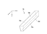
- FIG. 12 is a perspective view showing an example of a prism structure used in the backlight according to the present embodiment.
- FIG. 13 is a perspective view showing another example of the prism structure.
- the same components as those in FIG. 1 used in the first embodiment are denoted by the same reference numerals, and detailed description thereof is omitted.
- a plurality of grooves having a triangular cross-sectional shape are formed on the main surface (lower main surface) opposite to the light exit surface of the light guide. It was.
- a plurality of prism structures 68 (concavo-convex structures) whose cross-sectional shape along the xz plane is inverted to a trapezoid are formed on the light exit surface 67a of the light guide 67. ) Is formed.
- the extending direction of each prism structure 68 is substantially parallel to the y-axis direction, and the plurality of prism structures 68 are provided substantially parallel to each other. It is desirable that the refractive index of the light guide 67 and the refractive index of the prism structure 68 are substantially equal.
- the LED 5 is installed on the light incident end surface 67 b of the light guide 67.
- the prism structure 68 has a light incident end surface 68a, a light exit end surface 68b, and two inclined surfaces 68e and 68f.
- the two inclined surfaces 68e and 68f are inclined so as to form an angle other than perpendicular to the light incident end surface 68a and the light emitting end surface 68b.
- the inclined surface 68e far from the light incident end surface 67b of the light guide 67 provided with the LED 5 is a reflection that reflects the light incident from the light guide 67. Functions as a surface. Therefore, the light that has entered the prism structure 68 from the light guide 67 is reflected by the inclined surface 68e and then emitted from the light exit end surface 68b.
- the material cost can be reduced by reducing the number of parts and the manufacturing cost required for polarizing plate attaching work can be reduced, and the cost of the entire liquid crystal display device can be reduced.
- the same effects as those of the first to fourth embodiments can be obtained.
- the side surface 70f on the side close to the light incident end surface 67b does not contribute to light reflection, and therefore may be substantially perpendicular to the light incident end surface 70a and the light emitting end surface 70b.
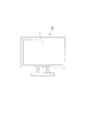
- FIG. 14 is a front view illustrating a schematic configuration of a liquid crystal display device which is a configuration example of the display device.
- the liquid crystal television 75 of this configuration example includes the liquid crystal display device 1 of the above embodiment as a display screen.
- a liquid crystal panel is disposed on the viewer side (front side in FIG. 14), and a backlight (light source device) is disposed on the side opposite to the viewer (back side in FIG. 14).
- the liquid crystal television 75 of this configuration example is a low-cost, high-contrast liquid crystal television by including the liquid crystal display device 1 of the above embodiment.
- the reflecting surface of the light guide is configured by a slope of a groove having a triangular cross-section, but instead of this configuration, the slope of a ridge (uneven structure) having a triangular cross-section is provided. It may be configured.
- the backlight includes one LED, the backlight may include a plurality of LEDs.
- the material, shape, arrangement, number, and the like of each component of the liquid crystal display device can be appropriately changed.
- a polarizing plate may be provided between the liquid crystal cell and the backlight.
- the aspect of the present invention can be used for a liquid crystal display device used in a display unit of various electronic devices.
Landscapes
- Physics & Mathematics (AREA)
- General Physics & Mathematics (AREA)
- Optics & Photonics (AREA)
- Nonlinear Science (AREA)
- Liquid Crystal (AREA)
- Mathematical Physics (AREA)
- Chemical & Material Sciences (AREA)
- Crystallography & Structural Chemistry (AREA)
- Planar Illumination Modules (AREA)
Abstract
液晶表示装置は、光源装置と、第一偏光板と、前記光源装置と前記第一偏光板との間に設けられ、前記光源装置から射出される光を変調する液晶セルと、を備え、前記光源装置が、偏光軸を有する偏光を発する発光部と、入射した前記発光部からの偏光が入射される端面と、前記偏光を反射させる反射面と、反射した前記偏光が射出する光射出面とを有し、低複屈折性を有する光透過性材料からなる導光体と、を備え、前記発光部から前記導光体に入射する前記偏光の前記偏光軸が、前記導光体の前記光射出面に対して略平行もしくは略垂直となるよう、前記発光部が前記導光部に対し配置されている。
Description
本発明は、液晶表示装置および光源装置に関する。
本願は、2011年2月24日に、日本に出願された特願2011-038385号に基づき優先権を主張し、その内容をここに援用する。
本願は、2011年2月24日に、日本に出願された特願2011-038385号に基づき優先権を主張し、その内容をここに援用する。
携帯電話機等をはじめとする携帯型電子機器、もしくはテレビジョン、パーソナルコンピューター等のディスプレイとして、液晶表示装置が広く用いられている。特に透過型の液晶表示装置では、液晶セルの背面側に配置した面発光光源から射出される光を利用して表示を行っている。本明細書において、この種の面発光光源のことをバックライトと称することもある。
下記の特許文献1には、偏光を発する偏光光源と、リタデーションが偏光の波長の1/4以下の低複屈折性を有する光透過性樹脂からなる導光板と、を備えた面発光装置が開示されている。さらに、特許文献1には、上記の面発光装置と、偏光子としての偏光板と、液晶セルと、検光子としての偏光板と、を備えた液晶表示装置が開示されている。
液晶表示装置の分野では、製造コストの低減や表示品位の向上が望まれている。しかしながら、特許文献1に記載された液晶表示装置は、使用する部品点数が従来と変わっておらず、製造コストが削減できるものではない。また、特許文献1に記載された面発光装置では、偏光の乱れを抑制する効果が不十分であり、液晶表示装置に適用した場合に表示のコントラストが低下する虞がある。
本発明の一態様は、上記の課題の少なくとも一つを解決するためになされたものであり、製造コストの低減、もしくは表示のコントラストの向上を図り得る液晶表示装置の提供を目的とする。また、この種の液晶表示装置に用いて好適な光源装置の提供を目的とする。
本発明の一態様における液晶表示装置は、光源装置と、第一偏光板と、前記光源装置と前記第一偏光板との間に設けられ、前記光源装置から射出される光を変調する液晶セルと、を備え、前記光源装置が、偏光軸を有する偏光を発する発光部と、前記発光部から入射した偏光が入射される端面と、前記偏光を反射させる反射面と、反射した前記偏光が射出する光射出面とを有し、低複屈折性を有する光透過性材料からなる導光体と、を備え、前記発光部から前記導光体に入射する前記偏光の前記偏光軸が、前記導光体の前記光射出面に対して略平行もしくは略垂直となるよう、前記発光部が前記導光部に対し配置されている。
本発明の一態様における液晶表示装置は、前記第一偏光板が前記液晶セルの光射出側にのみ設けられていてもよい。
本発明の一態様における液晶表示装置は、前記液晶セルが、液晶層を有し、前記液晶セルは、前記液晶層と前記光源装置との間に第二偏光板を有してもよい。
本発明の一態様における液晶表示装置は、前記導光体が凹凸構造体を有し、前記反射面が前記凹凸構造体の傾斜面からなり、前記凹凸構造体の延在方向が前記発光素子から射出される偏光の進行方向と略直交していてもよい。
本発明の一態様における液晶表示装置は、前記発光部を構成する発光素子が、非極性面または半極性面を主面とするIII族窒化半導体材料により構成されていてもよい。
本発明の一態様における液晶表示装置は、前記導光体が、正の複屈折物質と負の複屈折物質との混合体、もしくは正の複屈折物質と負の複屈折物質との共重合体により構成されていてもよい。
本発明の他の態様における光源装置は、偏光軸を有する偏光を発する発光部と、前記発光部から入射した偏光が入射される端面と、前記偏光を反射させる反射面と、反射した前記偏光が射出する光射出面とを有し、低複屈折性を有する光透過性材料からなる導光体と、を備え、前記発光部から前記導光体に入射する前記偏光の前記偏光軸が、前記導光体の前記光射出面に対して略平行もしくは略垂直となるよう、前記発光部が前記導光部に対し配置されている。
本発明の態様によれば、製造コストの低減、もしくは表示のコントラストの向上を図り得る液晶表示装置を提供することができる。本発明の態様によれば、この種の液晶表示装置に用いて好適な光源装置を提供することができる。
〔第1実施形態〕
以下、本発明の第1実施形態について、図1~図4Bを用いて説明する。
本実施形態では、バックライトと透過型の液晶セルとを備えた液晶表示装置の例を挙げて説明する。
以下、本発明の第1実施形態について、図1~図4Bを用いて説明する。
本実施形態では、バックライトと透過型の液晶セルとを備えた液晶表示装置の例を挙げて説明する。
図1は、本実施形態の液晶表示装置を示す斜視図である。図2は、本実施形態の光源装置に用いられるLEDを示す断面図である。図3は、本実施形態の液晶表示装置の液晶セルの部分を示す断面図である。図4Aおよび4Bは、本実施形態のバックライトの作用を説明するための図である。図4Aは、xy平面の法線方向から見た平面図である。図4Bは、xz平面に沿って切断したときの断面図である。
なお、以下の全ての図面においては、各構成要素を見やすくするため、構成要素によって寸法の縮尺を異ならせて示すことがある。
各図において、x軸は液晶表示装置の画面の水平方向(走査線の延在方向)、y軸は液晶表示装置の画面の垂直方向(走査線の延在方向に垂直な方向)、z軸は液晶表示装置の厚さ方向、と定義する。
なお、以下の全ての図面においては、各構成要素を見やすくするため、構成要素によって寸法の縮尺を異ならせて示すことがある。
各図において、x軸は液晶表示装置の画面の水平方向(走査線の延在方向)、y軸は液晶表示装置の画面の垂直方向(走査線の延在方向に垂直な方向)、z軸は液晶表示装置の厚さ方向、と定義する。
本実施形態の液晶表示装置1は、図1に示すように、バックライト2(光源装置)と、液晶セル3と、偏光板4と、を備えている。バックライト2は、発光ダイオード(Light Emitting Diode, 以下、LEDと略記する)5と、導光体6と、を備えている。本実施形態のLED5(発光部)は、所定の偏光軸を有する偏光を発するものである。導光体6は、低複屈折性を有する光透過性材料から構成されている。LED5および導光体6の構成については後で詳しく述べる。図1では、液晶セル3を模式的に1枚の板状に図示しているが、その詳細な構造は後で説明する。
本実施形態の液晶表示装置1においては、バックライト2から射出された光を液晶セル3で変調し、変調した光によって所定の画像や文字等を表示する。観察者は、偏光板4が配置された図1における液晶表示装置1の上方から画像や文字を見ることになる。よって、以下の説明では、偏光板4が配置された側を視認側と称し、バックライト2が配置された側を背面側と称する。
以下、バックライト2の構成について説明する。
本実施形態の導光体6は、その形状が板状であり、2つの主面と4つの端面とを有している。導光体6の2つの主面のうち、図1に示す上側の主面6aは光L2が射出される面である。導光体6の4つの端面のうちの1つの端面6bにLED5が配置されており、LED5が配置された導光体6の端面6bから光L1が入射する。導光体6の2つの主面のうち、図1に示す下側の主面6cには、図4Aおよび4Bに示すように、xz平面に沿う断面形状が三角形の複数の溝7(凹凸構造体)が形成されている。各溝7の延在方向はy軸方向に略平行であり、複数の溝7は互いに略平行に設けられている。溝7の内面となる2つの斜面のうち、LED5からの光L1の進行方向に対向する面7aが反射面として機能する。よって、導光体6の端面6bから入射した光は、反射面7aで反射してその進行方向を変え、主面6aから射出される。以下の説明では、導光体6の2つの主面のうち、光が射出される主面6aのことを「光射出面」と称する。導光体6の4つの端面のうち、光が入射される端面6bのことを「光入射端面」と称する。
本実施形態の導光体6は、その形状が板状であり、2つの主面と4つの端面とを有している。導光体6の2つの主面のうち、図1に示す上側の主面6aは光L2が射出される面である。導光体6の4つの端面のうちの1つの端面6bにLED5が配置されており、LED5が配置された導光体6の端面6bから光L1が入射する。導光体6の2つの主面のうち、図1に示す下側の主面6cには、図4Aおよび4Bに示すように、xz平面に沿う断面形状が三角形の複数の溝7(凹凸構造体)が形成されている。各溝7の延在方向はy軸方向に略平行であり、複数の溝7は互いに略平行に設けられている。溝7の内面となる2つの斜面のうち、LED5からの光L1の進行方向に対向する面7aが反射面として機能する。よって、導光体6の端面6bから入射した光は、反射面7aで反射してその進行方向を変え、主面6aから射出される。以下の説明では、導光体6の2つの主面のうち、光が射出される主面6aのことを「光射出面」と称する。導光体6の4つの端面のうち、光が入射される端面6bのことを「光入射端面」と称する。
上述したように、本実施形態のLED5は偏光を発するものである。「偏光」とは振動方向が特定の方向に偏りを有する光のことである。ところが、本実施形態の場合、必ずしも全ての偏光成分が一つの方向に揃った振動方向を有している必要はない。すなわち、100%の直線偏光である必要はない。したがって、光の偏光軸とは、その光の中に最も多く含まれる直線偏光成分の振動方向と定義する。
LED5は、図2に示すように、半導体基板36と、その上に順次積層された第1導電型の第1半導体層37、活性層38、第2導電型の第2半導体層39とを有している。半導体基板36はGaN単結晶からなり、その主面36aがGaN結晶の非極性面(Non-polarPlane)または半極性面(Semi-polarPlane)で構成されている。第1半導体層37、活性層38、および第2半導体層39は 半導体基板36の主面36aを結晶成長表面として使用し、この上に半導体材料を結晶成長させたものである。例えば結晶成長表面を非極性面であるm面とすると、LED5は、m面を主面とする窒化アルミニウム(AlN)、窒化ガリウム(GaN)、窒化インジウム(InN)等のIII族窒化物半導体により構成される。代表的なIII族窒化物半導体はAlxInyGa1-x-yN(0≦x≦1、0≦y≦1、0≦x+y≦1)により表される。GaN半導体は、窒素を含む六方晶化合物半導体の中でもよく知られたIII-V族化合物半導体である。
活性層38には、第1半導体層37から第1導電型のキャリアが供給され、第2半導体層39から第2導電型のキャリアが供給される。第1導電型がn型であり、第2導電型がp型である場合、第1半導体層37から供給される電子と第2半導体層39から供給される正孔とが活性層38で再結合し、活性層38から光L1が発せられる。活性層38には、例えばウェル層よりもバンドギャップの大きなバリア層でウェル層を挟持させた量子井戸(QuantumWell)構造、さらには多重量子井戸(MQW)構造を採用することができる。仮に活性層がGaN結晶の極性面を結晶成長表面とするIII族窒化物半導体であったとすると、その活性層からはランダム偏光(無偏光)状態の光が発せられる。一方、非極性面または半極性面を結晶成長表面とするIII族窒化物半導体を用いて形成した活性層38からは偏光状態の光L1が発生する。
LED5は、第1半導体層37に動作電圧を供給する第1電極40と、第2半導体層39に動作電圧を供給する第2電極41と、を備えている。第2半導体層39、活性層38、および第1半導体層37の厚さ方向の一部が除去されて第1半導体層37が露出された表面上に、第1電極40が形成されている。第1電極40の材料に例えばアルミニウム(Al)が用いられる。第2電極41の材料には例えばパラジウム(Pd)-金(Au)合金が用いられる。第1電極40は第1半導体層37にオーミック接続され、第2電極41は第2半導体層39にオーミック接続されている。なお、第1半導体層37と第1電極40との間に第1導電型のコンタクト層を介在させてもよい。また、第2半導体層39と第2電極41との間に第2導電型のコンタクト層を介在させてもよい。
本実施形態においては、光L1は半導体基板36の裏面から外部に射出されるものとする。したがって、LED5と導光体6とは、LED5を構成する半導体基板36の裏面が導光体6の光入射端面6bに対向する向きで固定される。また、本実施形態では、光L1の射出方向が略一方向に制御された指向性の高いLED5が用いられる。
導光体6は、低複屈折性を有する光透過性の樹脂材料で構成されている。なお、本明細書において、「低複屈折性」とは、光L1が導光体6に入射してから射出されるまでの光路において、光が受けるリタデーションが光の波長の1/4以下であることを言う。本実施形態において、リタデーションが光の波長の1/4以下であるような低複屈折性を有する樹脂材料は、正の複屈折物質と負の複屈折物質との混合体、もしくは正の複屈折物質と負の複屈折物質との共重合体で構成される。
具体的には、正の複屈折物質として、例えばポリビニリデンフルオライド(PVDF)、ポリビニリデンフルオライドトリフルオロエチレン(VDF・TrFE-58)、ポリエチレンオキサイド(PEO)などから選ばれるものを用いることが好ましいが、これらに限定されるものではない。負の複屈折物質としては、例えばポリメチルメタクリレート(PMMA)であることが好ましいが、これに限定されるものではない。なお、正の複屈折物質および負の複屈折物質は、上に挙げた複数の物質のうちの1種類でも良いし、複数種を組み合わせても良い。
あるいは、リタデーションが光の波長の1/4以下の低複屈折性材料として、棒状の分子形状で分極率に異方性を有する低分子有機物がポリマーに添加されたものを用いることができる。あるいは、ポリマーに無機複屈折性結晶微粒子が添加されたものを用いることもできる。
以下、液晶セル3の構成について説明する。
ここでは、アクティブマトリクス方式の透過型液晶セルを一例に挙げて説明するが、本実施形態に適用可能な液晶セルはアクティブマトリクス方式の透過型液晶セルに限るものではない。本実施形態に適用可能な液晶セルは、例えば半透過型(透過及び反射兼用型)液晶セルや反射型液晶セルであっても良く、更には、各画素がスイッチング用薄膜トランジスタ(Thin Film Transistor,以下、TFTと略記する)を備えていない単純マトリクス方式の液晶セルであっても良い。
ここでは、アクティブマトリクス方式の透過型液晶セルを一例に挙げて説明するが、本実施形態に適用可能な液晶セルはアクティブマトリクス方式の透過型液晶セルに限るものではない。本実施形態に適用可能な液晶セルは、例えば半透過型(透過及び反射兼用型)液晶セルや反射型液晶セルであっても良く、更には、各画素がスイッチング用薄膜トランジスタ(Thin Film Transistor,以下、TFTと略記する)を備えていない単純マトリクス方式の液晶セルであっても良い。
図3は、液晶セル3の縦断面図である。
液晶セル3は、図3に示すように、スイッチング素子基板としてのTFT基板9と、TFT基板9に対向して配置されたカラーフィルター基板10と、TFT基板9とカラーフィルター基板10との間に挟持された液晶層11と、を有している。液晶層11は、TFT基板9と、カラーフィルター基板10と、TFT基板9とカラーフィルター基板10とを所定の間隔をおいて貼り合わせる枠状のシール部材(図示せず)と、によって囲まれた空間内に封入されている。
液晶セル3は、図3に示すように、スイッチング素子基板としてのTFT基板9と、TFT基板9に対向して配置されたカラーフィルター基板10と、TFT基板9とカラーフィルター基板10との間に挟持された液晶層11と、を有している。液晶層11は、TFT基板9と、カラーフィルター基板10と、TFT基板9とカラーフィルター基板10とを所定の間隔をおいて貼り合わせる枠状のシール部材(図示せず)と、によって囲まれた空間内に封入されている。
本実施形態の液晶セル3は、例えばVA(Vertical Alignment,垂直配向)モードで表示を行うものであり、液晶層11には誘電率異方性が負の垂直配向液晶が用いられる。TFT基板9とカラーフィルター基板10との間には、これら基板間の間隔を一定に保持するための球状のスペーサー12が配置されている。なお、表示モードについては、上記のVAモードに限らず、TN(Twisted Nematic)モード、STN(Super Twisted Nematic)モード、IPS(In-Plane Switching)モード等を用いることができる。
TFT基板9には、表示の最小単位領域である画素(図示せず)がマトリクス状に複数配置されている。TFT基板9には、複数のソースバスライン(図示せず)が、互いに略平行に延在するように形成されるとともに、複数のゲートバスライン(図示せず)が、互いに略平行に延在し、かつ、複数のソースバスラインと直交するように形成されている。したがって、TFT基板9上には、複数のソースバスラインと複数のゲートバスラインとが格子状に形成され、隣接するソースバスラインと隣接するゲートバスラインとによって区画された矩形状の領域が一つの画素となる。ソースバスラインは、後述するTFTのソース電極に接続され、ゲートバスラインは、TFTのゲート電極に接続されている。
TFT基板9を構成する透明基板14の液晶層11側の面に、半導体層15、ゲート電極16、ソース電極17、ドレイン電極18等を有するTFT19が形成されている。透明基板14には、例えばガラス基板を用いることができる。透明基板14上に、例えばCGS(Continuous Grain Silicon:連続粒界シリコン)、LPS(Low-temperature Poly-Silicon:低温多結晶シリコン)、α-Si(Amorphous Silicon:非結晶シリコン)等の半導体材料からなる半導体層15が形成されている。透明基板14上に、半導体層15を覆うようにゲート絶縁膜20が形成されている。ゲート絶縁膜20の材料としては、例えばシリコン酸化膜、シリコン窒化膜、もしくはこれらの積層膜等が用いられる。ゲート絶縁膜20上には、半導体層15と対向するようにゲート電極16が形成されている。ゲート電極16の材料としては、例えばW(タングステン)/TaN(窒化タンタル)の積層膜、Mo(モリブデン)、Ti(チタン)、Al(アルミニウム)等が用いられる。
ゲート絶縁膜20上に、ゲート電極16を覆うように第1層間絶縁膜21が形成されている。第1層間絶縁膜21の材料としては、例えばシリコン酸化膜、シリコン窒化膜、もしくはこれらの積層膜等が用いられる。第1層間絶縁膜21上に、ソース電極17およびドレイン電極18が形成されている。ソース電極17は、第1層間絶縁膜21とゲート絶縁膜20とを貫通するコンタクトホール22を介して半導体層15のソース領域に接続されている。同様に、ドレイン電極18は、第1層間絶縁膜21とゲート絶縁膜20とを貫通するコンタクトホール23を介して半導体層15のドレイン領域に接続されている。ソース電極17およびドレイン電極18の材料としては、上述のゲート電極16と同様の導電性材料が用いられる。第1層間絶縁膜21上に、ソース電極17およびドレイン電極18を覆うように第2層間絶縁膜24が形成されている。第2層間絶縁膜24の材料としては、上述の第1層間絶縁膜21と同様の材料、もしくは有機絶縁性材料が用いられる。
第2層間絶縁膜24上に、画素電極25が形成されている。画素電極25は、第2層間絶縁膜24を貫通するコンタクトホール26を介してドレイン電極18に接続されている。よって、画素電極25は、ドレイン電極18を中継用電極として半導体層15のドレイン領域に接続されている。画素電極25の材料としては、例えばITO(Indium Tin Oxide、インジウム錫酸化物)、IZO(Indium Zinc Oxide、インジウム亜鉛酸化物)等の透明導電性材料が用いられる。この構成により、ゲートバスラインを通じて走査信号が供給され、TFT19がオン状態となったときに、ソースバスラインを通じてソース電極17に供給された画像信号が、半導体層15、ドレイン電極18を経て画素電極25に供給される。また、画素電極25を覆うように第2層間絶縁膜24上のに配向膜27が形成されている。この配向膜27は、液晶層11を構成する液晶分子を垂直配向させる配向規制力を有している。なお、TFTの形態としては、図3に示したボトムゲート型TFTであっても良いし、トップゲート型TFTであっても良い。
一方、カラーフィルター基板10を構成する透明基板29の液晶層11側の面には、ブラックマトリクス30、カラーフィルター31、平坦化層32、対向電極33、配向膜34が順次形成されている。ブラックマトリクス30は、画素間領域において光の透過を遮断する機能を有している。ブラックマトリクス30は、Cr(クロム)やCr/酸化Crの多層膜等の金属、もしくはカーボン粒子を感光性樹脂に分散させたフォトレジストで形成されている。カラーフィルター31には、赤色(R)、緑色(G)、青色(B)の各色の色素が含まれており、TFT基板9上の一つの画素電極25にR,G,Bのいずれか一つのカラーフィルター31が対向して配置されている。平坦化層32は、ブラックマトリクス30およびカラーフィルター31を覆う絶縁膜で構成されており、ブラックマトリクス30およびカラーフィルター31によってできる段差を緩和して平坦化する機能を有している。平坦化層32上には対向電極33が形成されている。対向電極33の材料としては、画素電極25と同様の透明導電性材料が用いられる。また、対向電極33上の全面に、垂直配向規制力を有する配向膜34が形成されている。カラーフィルター31は、R、G、Bの3色以上の多色構成としても良い。
本実施形態の液晶表示装置1においては、図1に示すように、液晶セル3の視認側に、液晶セル3によって変調された光の透過/遮断を規制するための偏光板4が設けられている。図1では、液晶セル3と偏光板4とを離して描いてあるが、実際には液晶セル3を構成するカラーフィルター基板10の一面に粘着層等を介して偏光板4が貼り合わされていても良い。これに対して、バックライト2と液晶セル3との間には、液晶セル3に入射する光の偏光軸を規制するための偏光板が設けられていない。
本実施形態の液晶表示装置1において、図4A及び4Bに示すように、LED5から導光体6に入射する光L1の偏光軸が、導光体6の光射出面6a(xy平面)に対して略平行であって光入射端面6bに対して略平行(y軸方向)に配置されるように、導光体6に対するLED5の向きが設定されている。このときの光L1の偏光方向p1を図4A及び4Bの符号Aの円内に示す。本実施形態では指向性の高いLED5が用いられているため、導光体6の内部で光入射端面6bに対して略垂直な方向(x軸方向)に光L1は進行する。導光体6が低複屈折性を有する光透過性樹脂材料で構成されているため、光L1が導光体6内部を進行している間、光L1の偏光軸方向は略入射時の方向p1に維持されたままである。なお、図4A及び4Bでは、説明の都合上、LED5と導光板6とを離して描いている。
導光体6の溝7(反射面7a)は光入射端面6bの延在方向と略平行な方向(y軸方向)に延在しているため、導光体6の内部を進行する光L1は、反射面7aの延在方向に対して略垂直な方向(x軸方向)から反射面7aに入射して反射する。散乱材等を用いて光を散乱させて外部に射出させる方式の導光体の場合、散乱によって光の偏光軸の方向が乱れてしまい、偏光軸の方向が維持されない。これに対し、本実施形態のように、反射面で光を反射させて外部に射出させる方式の導光体6の場合、反射後の光L2の偏光軸の方向は反射前と変わらない。したがって、反射面7aで反射して進行方向を変えた後、光射出面6aから外部に射出される光L2の偏光軸は、導光体6の光射出面6aに対して略平行、かつ光入射端面6bに対して略平行な方向が維持されている。このときの光L2の偏光方向p2を図4A及び4Bの符号Bの円内に示す。このように、本実施形態のバックライト2によれば、偏光軸が略一方向に揃った偏光を射出させることができる。
本実施形態の液晶表示装置1の場合、図1に示すように、バックライト2から液晶セル3に入射される光L2の偏光軸の方向p2はy軸方向であるのに対し、液晶セル3の視認側の偏光板4の透過軸方向p4がx軸方向である。すなわち、液晶セル3に入射される光L2の偏光軸の方向p2と偏光板4の透過軸方向p4とが直交するように配置されている。したがって、液晶セル3に電圧が印加されていないとき、偏光板4の透過軸方向p4と直交する偏光軸を持つ光L3は偏光板4を透過できず、黒表示となる。一方、液晶セル3に電圧が印加されたとき、液晶セル3から射出された光L3は偏光板4の透過軸方向p4に一致する偏光成分が偏光板4を透過し、白表示となる。このようにして、本実施形態の液晶表示装置1ではノーマリーブラックモードの表示が行われる。
図1に示す状態から偏光板4をxy平面内で90度回転させ、液晶セル3に入射される光L2の偏光軸の方向p2と偏光板4の透過軸方向p4とが略平行になるように配置すれば、ノーマリーホワイトモードの表示を行うこともできる。
本実施形態の液晶表示装置1においては、バックライト2から偏光軸が略一方向に揃った偏光が射出されるため、従来一般の液晶表示装置で用いられていたバックライトと液晶セルとの間の偏光板をなくすことができる。その結果、部品点数が減ることによる材料費の削減、偏光板貼付作業に要する製造コストの削減が図れ、液晶表示装置全体のコストを低減することが可能となる。
なお、本実施形態のバックライト2では、非極性面または半極性面を主面とするIII族窒化半導体材料からなり、直線偏光を直接発するLED5を用いた。その構成に代えて、偏光状態がランダムな光を発するLEDの光射出面に偏光板を貼付した構成とし、偏光板を通して光を射出させることで直線偏光を発するLEDを用いても良い。
〔第2実施形態〕
以下、本発明の第2実施形態について、図5~図6Bを用いて説明する。
本実施形態の液晶表示装置の基本構成は第1実施形態と同様である。導光体に対する光の偏光軸の方向が第1実施形態と異なる。
図5は、本実施形態の液晶表示装置を示す斜視図である。図6A及び6Bは、本実施形態のバックライトの作用を説明するための図である。図6Aは、xy平面の法線方向から見た平面図である。図6Bは、xz平面に沿って切断したときの断面図である。
図5~図6Bにおいて、第1実施形態で用いた図1、図4A、及び図4Bと共通の構成要素には同一の符号を付し、詳細な説明は省略する。
以下、本発明の第2実施形態について、図5~図6Bを用いて説明する。
本実施形態の液晶表示装置の基本構成は第1実施形態と同様である。導光体に対する光の偏光軸の方向が第1実施形態と異なる。
図5は、本実施形態の液晶表示装置を示す斜視図である。図6A及び6Bは、本実施形態のバックライトの作用を説明するための図である。図6Aは、xy平面の法線方向から見た平面図である。図6Bは、xz平面に沿って切断したときの断面図である。
図5~図6Bにおいて、第1実施形態で用いた図1、図4A、及び図4Bと共通の構成要素には同一の符号を付し、詳細な説明は省略する。
本実施形態の液晶表示装置43においても、第1実施形態と同様、図5に示すように、液晶セル3の視認側に偏光板4が設けられ、バックライト44と液晶セル3との間には、偏光板が設けられていない。液晶セル3の視認側の偏光板4の透過軸方向p4はy軸方向に設定されている。
本実施形態の液晶表示装置43において、図6A及び6Bに示すように、LED5から導光体6に入射する光L1の偏光軸p1が、導光体6の光射出面6a(xy平面)に対して垂直(z軸方向)に配置されるように、導光体6に対するLED5の向きが設定されている。このときの光L1の偏光方向p1を図6A及び6Bの符号Aの円内に示す。本実施形態では指向性の高いLED5が用いられているため、導光体6の内部で光入射端面6bに対して略垂直な方向(x軸方向)に光L1は進行する。導光体6が低複屈折性を有する光透過性樹脂材料で構成されているため、光L1が導光体6内部を進行している間、光L1の偏光軸方向は略入射時の方向p1に維持されたままである。
導光体6の溝7(反射面7a)は光入射端面6bの延在方向と略平行な方向(y軸方向)に延在しているため、導光体6の内部を進行する光L1は、反射面7aの延在方向に対して略垂直な方向(x軸方向)から反射面7aに入射して反射する。本実施形態の場合、反射面7aで反射した後の光L2の偏光軸の方向p2は、光L2の光軸側から見たときには反射前と変わらない。ただし、光の進行方向が略90度変わることにより外部から見たときの光L2の偏光軸の方向p2は入射時の偏光軸の方向p1に対して略90度回転し、x軸方向となる。このときの光L2の偏光方向p2を図6A及び6Bの符号Bの円内に示す。このように、本実施形態のバックライト44によれば、偏光軸が略一方向に揃った偏光を射出させることができる。
本実施形態の液晶表示装置43においても、部品点数が減ることによる材料費の削減や偏光板貼付作業に要する製造コストの削減が図れ、液晶表示装置全体のコストを低減できる、といった第1実施形態と同様の効果が得られる。
〔第3実施形態〕
以下、本発明の第3実施形態について、図7、図8を用いて説明する。
本実施形態の液晶表示装置の基本構成は第1実施形態と同様である。導光体に対する光の偏光軸の方向が第1実施形態と異なる。
図7は、本実施形態の液晶表示装置を示す斜視図である。図8は、本実施形態の液晶セルの断面図である。
図7、図8において、第1実施形態で用いた図1、図3と共通の構成要素には同一の符号を付し、詳細な説明は省略する。
以下、本発明の第3実施形態について、図7、図8を用いて説明する。
本実施形態の液晶表示装置の基本構成は第1実施形態と同様である。導光体に対する光の偏光軸の方向が第1実施形態と異なる。
図7は、本実施形態の液晶表示装置を示す斜視図である。図8は、本実施形態の液晶セルの断面図である。
図7、図8において、第1実施形態で用いた図1、図3と共通の構成要素には同一の符号を付し、詳細な説明は省略する。
本実施形態の液晶表示装置46においても、第1、第2実施形態と同様、図7に示すように、液晶セル47の視認側に偏光板4が設けられ、バックライト2と液晶セル47との間には、偏光板が設けられていない。液晶セル47の視認側の偏光板4の透過軸方向はx軸方向に設定されている。
液晶セル47は、図8に示すように、TFT基板9を構成する透明基板14の液晶層11側の面に偏光板48が形成されている。偏光板48は、例えば光の波長程度の間隔で形成された多数の微細金属線からなるワイヤーグリッド、もしくは2色性色素の層が透明基板14上に直接形成されたものである。この偏光板48は液晶セル47内に形成されており、液晶セル外部の偏光板4と区別するため、以下の説明では「セル内偏光板」と称する。本実施形態の液晶セル47は、セル内偏光板48が形成されたこと以外は図3に示す第1実施形態の液晶セル3と同様である。セル内偏光板48の透過軸方向は、図7に示すように、LED5から射出された光L1の偏光軸方向p1と略平行な方向p3(y軸方向)に設定されている。
本実施形態の液晶表示装置46においても、部品点数が減ることによる材料費の削減や偏光板貼付作業に要する製造コストの削減が図れ、液晶表示装置全体のコストを低減できる、といった第1、第2実施形態と同様の効果が得られる。
本実施形態のバックライト2も、第1、第2実施形態と同様、導光体6の材料に低複屈折性を有する光透過性材料が用いられている。よって、基本的には、光L1が導光体6内を進行する際に、光の偏光軸方向は入射時の方向p1に維持される。しかしながら、導光体6は複屈折性を僅かに有しているので、入射時の光の偏光軸方向p1とは異なる方向の偏光軸を持つ偏光成分が僅かながら発生する。その結果、バックライト2から射出される光L2は、図7に示すように、LED5から射出された光L1の偏光軸方向p1に略平行な偏光軸方向p2とそれ以外の偏光軸方向p2’とが混在した光となる。このような光L2によって表示を行うと、表示のコントラストが低下する。
ところが、本実施形態の液晶セル47にはセル内偏光板48が設けられているので、導光体6に入射した時の光L1の偏光軸方向p1とは異なる方向の偏光軸方向p2’を持つ偏光成分がセル内偏光板48により吸収もしくは反射される。したがって、液晶セル47内の液晶層11に光が入射する時点では光の偏光軸の方向が略一方向に揃っている。これにより、本実施形態の液晶表示装置46では、コスト低減の効果に加えて、表示のコントラストを高められるという効果を得ることができる。
〔第4実施形態〕
以下、本発明の第4実施形態について、図9、図10を用いて説明する。
本実施形態の液晶表示装置の基本構成は第1実施形態と同様である。液晶表示装置に用いられるバックライトの発光部の構成が第1実施形態と異なる。
図9は、本実施形態のバックライトを示す平面図である。図10は、本実施形態のバックライトの他の例を示す平面図である。
図9、図10において、第1実施形態で用いた図4Aと共通の構成要素には同一の符号を付し、詳細な説明は省略する。
以下、本発明の第4実施形態について、図9、図10を用いて説明する。
本実施形態の液晶表示装置の基本構成は第1実施形態と同様である。液晶表示装置に用いられるバックライトの発光部の構成が第1実施形態と異なる。
図9は、本実施形態のバックライトを示す平面図である。図10は、本実施形態のバックライトの他の例を示す平面図である。
図9、図10において、第1実施形態で用いた図4Aと共通の構成要素には同一の符号を付し、詳細な説明は省略する。
本実施形態のバックライト50は、図9に示すように、LED51と第1導光体52と偏光板53とからなる発光部54と、第2導光体55と、を備えている。LED51は、第1実施形態とは異なり、ランダムな方向に偏光軸を有する光を射出するものである。第1導光体52は、第2導光体55の光入射端面55bの寸法と略同じ長手寸法を有するプリズム構造体で構成されている。xy平面の法線方向から見た第1導光体52の平面形状は直角三角形であり、互いに直交する2つの面がLED51の設置面52bおよび光射出面52aであり、斜面がLEDからの光を反射させる反射面52cである。第2導光体55は、第1実施形態と同様の導光体6の光入射端面に複数のプリズム構造体56が設けられたものである。第1導光体52の光射出面52aと第2導光体55のプリズム構造体56との間に偏光板53が設けられている。
本実施形態のバックライト50の場合、LED51から射出された光はランダムな方向に偏光軸を有しており、この光が第1導光体52に入射された後、反射面52cで反射して光射出面52aから射出される。その後、ランダムな方向に偏光軸を有する光のうち、偏光板53の透過軸に一致する方向に偏光軸を有する偏光成分のみが偏光板53を透過することにより、偏光軸が略一方向に揃った光となる。そして、この光が第2導光体55のプリズム構造体56から入射されると、プリズム構造体56における全反射角近傍の光を第2構造体55から取り出すことができる。このようにして、偏光軸が略一方向に揃い、指向性の高い平行光を生成することができる。
本実施形態の他のバックライト58は、図10に示すように、LED51と第1導光体59と偏光板53とからなる発光部60と、第2導光体55と、を備えている。図10に示すバックライト58の基本構成は、図9に示すバックライト50と略同様であり、第1導光体59の形状のみが異なっている。図9に示す第1導光体52は全体が一つのプリズム形状であったのに対し、図10に示す第1導光体59は矩形の導光部61の長辺に沿って複数のプリズム構造体62が一体に設けられている。第1導光体59の複数のプリズム構造体62の斜面が反射面62cとなる。バックライト58における光の振る舞いについては図9に示すバックライト50と同様である。
本実施形態のバックライト50,58を用いた液晶表示装置においても、部品点数が減ることによる材料費の削減や偏光板貼付作業に要する製造コストの削減が図れ、液晶表示装置全体のコストを低減できる、といった第1~第3実施形態と同様の効果が得られる。
〔第5実施形態〕
以下、本発明の第5実施形態について、図11~図13を用いて説明する。
本実施形態の液晶表示装置の基本構成は第1実施形態と同様である。液晶表示装置に用いられるバックライトの導光体の構成が第1実施形態と異なる。
図11は、本実施形態の液晶表示装置を示す平面図である。図12は、本実施形態のバックライトに用いられるプリズム構造体の一例を示す斜視図である。図13は、プリズム構造体の他の例を示す斜視図である。
図11において、第1実施形態で用いた図1と共通の構成要素には同一の符号を付し、詳細な説明は省略する。
以下、本発明の第5実施形態について、図11~図13を用いて説明する。
本実施形態の液晶表示装置の基本構成は第1実施形態と同様である。液晶表示装置に用いられるバックライトの導光体の構成が第1実施形態と異なる。
図11は、本実施形態の液晶表示装置を示す平面図である。図12は、本実施形態のバックライトに用いられるプリズム構造体の一例を示す斜視図である。図13は、プリズム構造体の他の例を示す斜視図である。
図11において、第1実施形態で用いた図1と共通の構成要素には同一の符号を付し、詳細な説明は省略する。
第1~第4実施形態においては、導光体の光射出面と反対側の主面(下側の主面)には、断面形状が三角形の複数の溝(凹凸構造体)が形成されていた。これに対して、本実施形態のバックライト66においては、導光体67の光射出面67aに、xz平面に沿う断面形状が台形を逆さにした形状の複数のプリズム構造体68(凹凸構造体)が形成されている。各プリズム構造体68の延在方向はy軸方向に略平行であり、複数のプリズム構造体68は互いに略平行に設けられている。導光体67の屈折率とプリズム構造体68屈折率とは略等しいことが望ましい。第1実施形態と同様、導光体67の光入射端面67bには、LED5が設置されている。
プリズム構造体68は、図12に示すように、光入射端面68aと光射出端面68bと、2つの傾斜面68e,68fを有する。2つの傾斜面68e,68fは、光入射端面68aおよび光射出端面68bに対して垂直以外の角度をなすように傾斜している。プリズム構造体68の2つの傾斜面68e,68fのうち、LED5が設けられた導光体67の光入射端面67bから遠い側の傾斜面68eは、導光体67から入射した光を反射させる反射面として機能する。よって、導光体67からプリズム構造体68の内部に入射した光は、傾斜面68eで反射した後、光射出端面68bから射出される。
本実施形態のバックライト66を用いた液晶表示装置65においても、部品点数が減ることによる材料費の削減や偏光板貼付作業に要する製造コストの削減が図れ、液晶表示装置全体のコストを低減できる、といった第1~第4実施形態と同様の効果が得られる。
本実施形態では、2つの傾斜面を有するプリズム構造体68の例を示したが、この構成に代えて、例えば図13に示すプリズム構造体70のように、LED5が設けられた導光体67の光入射端面67bに近い側の側面70fは、光の反射に寄与しないため、光入射端面70aおよび光射出端面70bに対して略垂直であっても良い。
[表示装置の構成例]
以下、表示装置の一構成例について、図14を用いて説明する。
図14は、表示装置の一構成例である液晶表示装置の概略構成を示す正面図である。
本構成例の液晶テレビジョン75は、図14に示すように、表示画面として上記実施形態の液晶表示装置1を備えている。観察者側(図14の手前側)には液晶パネルが配置され、観察者と反対側(図14の奥側)にはバックライト(光源装置)が配置されている。
本構成例の液晶テレビジョン75は、上記実施形態の液晶表示装置1を備えたことで、低コスト、高コントラストの液晶テレビジョンとなる。
以下、表示装置の一構成例について、図14を用いて説明する。
図14は、表示装置の一構成例である液晶表示装置の概略構成を示す正面図である。
本構成例の液晶テレビジョン75は、図14に示すように、表示画面として上記実施形態の液晶表示装置1を備えている。観察者側(図14の手前側)には液晶パネルが配置され、観察者と反対側(図14の奥側)にはバックライト(光源装置)が配置されている。
本構成例の液晶テレビジョン75は、上記実施形態の液晶表示装置1を備えたことで、低コスト、高コントラストの液晶テレビジョンとなる。
なお、本発明の態様における技術範囲は、上記実施形態に限定されるものではなく、本発明の態様における趣旨を逸脱しない範囲において種々の変更を加えることが可能である。例えば上記実施形態では、導光体の反射面が、断面形状が三角形の溝の斜面で構成されていたが、この構成に代えて、断面形状が三角形の凸条(凹凸構造体)の斜面で構成されていても良い。バックライトが1個のLEDを備えていたが、複数個のLEDを備えていても良い。その他、液晶表示装置の各構成要素の材料、形状、配置、個数等に関しては適宜変更が可能である。なお、表示のコントラストをより高めるために、液晶セルとバックライトとの間に偏光板を備えていても良い。
本発明の態様は、各種電子機器などの表示部に用いられる液晶表示装置に利用可能である。
1,43,46,65…液晶表示装置、2,44,50,58,66…バックライト(光源装置)、3,47…液晶セル、4…偏光板、5,51…LED(発光部)、6,67…導光体、7…溝(凹凸構造体)、7a…反射面、48…セル内偏光板、54,60…発光部、68…プリズム構造体(凹凸構造体)。
Claims (7)
- 光源装置と、
第一偏光板と、
前記光源装置と前記第一偏光板との間に設けられ、前記光源装置から射出される光を変調する液晶セルと、を備え、
前記光源装置が、偏光軸を有する偏光を発する発光部と、入射した前記発光部からの偏光が入射される端面と、前記偏光を反射させる反射面と、反射した前記偏光が射出する光射出面とを有し、低複屈折性を有する光透過性材料からなる導光体と、を備え、
前記発光部から前記導光体に入射する前記偏光の前記偏光軸が、前記導光体の前記光射出面に対して略平行もしくは略垂直となるよう、前記発光部が前記導光部に対し配置されている液晶表示装置。 - 前記第一偏光板が前記液晶セルの光射出側にのみ設けられている請求項1に記載の液晶表示装置。
- 前記液晶セルは、液晶層を有し、前記液晶セルは、前記液晶層と前記光源装置との間に第二偏光板を有する請求項1に記載の液晶表示装置。
- 前記導光体は、凹凸構造体を有し、前記反射面は、前記凹凸構造体の傾斜面からなり、前記凹凸構造体の延在方向が前記発光素子から射出される偏光の進行方向と略直交している請求項1に記載の液晶表示装置。
- 前記発光部を構成する発光素子が、非極性面または半極性面を主面とするIII族窒化半導体材料により構成されている請求項1に記載の液晶表示装置。
- 前記導光体が、正の複屈折物質と負の複屈折物質との混合体、もしくは正の複屈折物質と負の複屈折物質との共重合体により構成されている請求項1に記載の液晶表示装置。
- 偏光軸を有する偏光を発する発光部と、前記発光部から入射した偏光が入射される端面と、前記偏光を反射させる反射面と、反射した前記偏光が射出する光射出面とを有し、低複屈折性を有する光透過性材料からなる導光体と、を備え、
前記発光部から前記導光体に入射する前記偏光の前記偏光軸が、前記導光体の前記光射出面に対して略平行もしくは略垂直となるよう、前期発光部が前記導光部に対し配置されている光源装置。
Applications Claiming Priority (2)
| Application Number | Priority Date | Filing Date | Title |
|---|---|---|---|
| JP2011-038385 | 2011-02-24 | ||
| JP2011038385 | 2011-02-24 |
Publications (1)
| Publication Number | Publication Date |
|---|---|
| WO2012114911A1 true WO2012114911A1 (ja) | 2012-08-30 |
Family
ID=46720693
Family Applications (1)
| Application Number | Title | Priority Date | Filing Date |
|---|---|---|---|
| PCT/JP2012/053142 Ceased WO2012114911A1 (ja) | 2011-02-24 | 2012-02-10 | 液晶表示装置および光源装置 |
Country Status (1)
| Country | Link |
|---|---|
| WO (1) | WO2012114911A1 (ja) |
Citations (2)
| Publication number | Priority date | Publication date | Assignee | Title |
|---|---|---|---|---|
| JP2004061619A (ja) * | 2002-07-25 | 2004-02-26 | Minolta Co Ltd | 偏光変換装置および照明光学系 |
| JP2009140916A (ja) * | 2007-11-12 | 2009-06-25 | Keio Gijuku | 面発光装置及び偏光光源 |
-
2012
- 2012-02-10 WO PCT/JP2012/053142 patent/WO2012114911A1/ja not_active Ceased
Patent Citations (2)
| Publication number | Priority date | Publication date | Assignee | Title |
|---|---|---|---|---|
| JP2004061619A (ja) * | 2002-07-25 | 2004-02-26 | Minolta Co Ltd | 偏光変換装置および照明光学系 |
| JP2009140916A (ja) * | 2007-11-12 | 2009-06-25 | Keio Gijuku | 面発光装置及び偏光光源 |
Similar Documents
| Publication | Publication Date | Title |
|---|---|---|
| KR102373327B1 (ko) | 액정 표시 장치 및 그 구동 방법 | |
| KR20130015471A (ko) | 디스플레이패널 및 이를 채용한 디스플레이장치 | |
| JP2018180290A (ja) | 表示装置 | |
| US20220082877A1 (en) | Imaging device having dimming element | |
| US7868974B2 (en) | Liquid crystal display device | |
| US10025141B2 (en) | Display component and display device | |
| US10705390B2 (en) | Color conversion substrate and liquid-crystal display device including the same | |
| US8786790B2 (en) | Liquid crystal display device | |
| JP5731892B2 (ja) | 表示装置 | |
| JP5380387B2 (ja) | 液晶表示装置 | |
| US20120293751A1 (en) | Liquid crystal device and electronic apparatus including the same | |
| JP2007041536A (ja) | 表示装置及び液晶表示装置 | |
| US9341906B2 (en) | Liquid crystal display device | |
| CN104641283A (zh) | 液晶显示装置 | |
| US20040196422A1 (en) | Semi-transmissive reflective color liquid crystal display device | |
| JP2012155068A (ja) | 表示パネル、表示装置および電子機器 | |
| JP2015125365A (ja) | 液晶表示装置 | |
| US20160170263A1 (en) | Liquid crystal display device | |
| JP2006184363A (ja) | 液晶表示装置 | |
| US10649296B2 (en) | Liquid crystal display device | |
| US9696581B2 (en) | Liquid crystal display device and electronic device | |
| WO2012114911A1 (ja) | 液晶表示装置および光源装置 | |
| JP2011064849A (ja) | 電気光学装置及び電子機器 | |
| JP6508817B2 (ja) | 液晶表示装置 | |
| WO2016163196A1 (ja) | 液晶表示装置 |
Legal Events
| Date | Code | Title | Description |
|---|---|---|---|
| 121 | Ep: the epo has been informed by wipo that ep was designated in this application |
Ref document number: 12749428 Country of ref document: EP Kind code of ref document: A1 |
|
| NENP | Non-entry into the national phase |
Ref country code: DE |
|
| 122 | Ep: pct application non-entry in european phase |
Ref document number: 12749428 Country of ref document: EP Kind code of ref document: A1 |
|
| NENP | Non-entry into the national phase |
Ref country code: JP |