WO2012114789A1 - 太陽電池及び太陽電池モジュール - Google Patents
太陽電池及び太陽電池モジュール Download PDFInfo
- Publication number
- WO2012114789A1 WO2012114789A1 PCT/JP2012/050669 JP2012050669W WO2012114789A1 WO 2012114789 A1 WO2012114789 A1 WO 2012114789A1 JP 2012050669 W JP2012050669 W JP 2012050669W WO 2012114789 A1 WO2012114789 A1 WO 2012114789A1
- Authority
- WO
- WIPO (PCT)
- Prior art keywords
- bus bar
- solar cell
- finger
- bar portion
- side bus
- Prior art date
- Legal status (The legal status is an assumption and is not a legal conclusion. Google has not performed a legal analysis and makes no representation as to the accuracy of the status listed.)
- Ceased
Links
Images



Classifications
-
- H—ELECTRICITY
- H10—SEMICONDUCTOR DEVICES; ELECTRIC SOLID-STATE DEVICES NOT OTHERWISE PROVIDED FOR
- H10F—INORGANIC SEMICONDUCTOR DEVICES SENSITIVE TO INFRARED RADIATION, LIGHT, ELECTROMAGNETIC RADIATION OF SHORTER WAVELENGTH OR CORPUSCULAR RADIATION
- H10F77/00—Constructional details of devices covered by this subclass
- H10F77/20—Electrodes
- H10F77/206—Electrodes for devices having potential barriers
- H10F77/211—Electrodes for devices having potential barriers for photovoltaic cells
- H10F77/219—Arrangements for electrodes of back-contact photovoltaic cells
-
- H—ELECTRICITY
- H10—SEMICONDUCTOR DEVICES; ELECTRIC SOLID-STATE DEVICES NOT OTHERWISE PROVIDED FOR
- H10F—INORGANIC SEMICONDUCTOR DEVICES SENSITIVE TO INFRARED RADIATION, LIGHT, ELECTROMAGNETIC RADIATION OF SHORTER WAVELENGTH OR CORPUSCULAR RADIATION
- H10F10/00—Individual photovoltaic cells, e.g. solar cells
- H10F10/10—Individual photovoltaic cells, e.g. solar cells having potential barriers
- H10F10/14—Photovoltaic cells having only PN homojunction potential barriers
- H10F10/146—Back-junction photovoltaic cells, e.g. having interdigitated base-emitter regions on the back side
-
- H—ELECTRICITY
- H10—SEMICONDUCTOR DEVICES; ELECTRIC SOLID-STATE DEVICES NOT OTHERWISE PROVIDED FOR
- H10F—INORGANIC SEMICONDUCTOR DEVICES SENSITIVE TO INFRARED RADIATION, LIGHT, ELECTROMAGNETIC RADIATION OF SHORTER WAVELENGTH OR CORPUSCULAR RADIATION
- H10F71/00—Manufacture or treatment of devices covered by this subclass
- H10F71/121—The active layers comprising only Group IV materials
-
- H—ELECTRICITY
- H10—SEMICONDUCTOR DEVICES; ELECTRIC SOLID-STATE DEVICES NOT OTHERWISE PROVIDED FOR
- H10F—INORGANIC SEMICONDUCTOR DEVICES SENSITIVE TO INFRARED RADIATION, LIGHT, ELECTROMAGNETIC RADIATION OF SHORTER WAVELENGTH OR CORPUSCULAR RADIATION
- H10F77/00—Constructional details of devices covered by this subclass
- H10F77/10—Semiconductor bodies
- H10F77/16—Material structures, e.g. crystalline structures, film structures or crystal plane orientations
- H10F77/162—Non-monocrystalline materials, e.g. semiconductor particles embedded in insulating materials
- H10F77/166—Amorphous semiconductors
- H10F77/1662—Amorphous semiconductors including only Group IV materials
-
- H—ELECTRICITY
- H10—SEMICONDUCTOR DEVICES; ELECTRIC SOLID-STATE DEVICES NOT OTHERWISE PROVIDED FOR
- H10F—INORGANIC SEMICONDUCTOR DEVICES SENSITIVE TO INFRARED RADIATION, LIGHT, ELECTROMAGNETIC RADIATION OF SHORTER WAVELENGTH OR CORPUSCULAR RADIATION
- H10F77/00—Constructional details of devices covered by this subclass
- H10F77/20—Electrodes
- H10F77/206—Electrodes for devices having potential barriers
- H10F77/211—Electrodes for devices having potential barriers for photovoltaic cells
- H10F77/215—Geometries of grid contacts
-
- Y—GENERAL TAGGING OF NEW TECHNOLOGICAL DEVELOPMENTS; GENERAL TAGGING OF CROSS-SECTIONAL TECHNOLOGIES SPANNING OVER SEVERAL SECTIONS OF THE IPC; TECHNICAL SUBJECTS COVERED BY FORMER USPC CROSS-REFERENCE ART COLLECTIONS [XRACs] AND DIGESTS
- Y02—TECHNOLOGIES OR APPLICATIONS FOR MITIGATION OR ADAPTATION AGAINST CLIMATE CHANGE
- Y02E—REDUCTION OF GREENHOUSE GAS [GHG] EMISSIONS, RELATED TO ENERGY GENERATION, TRANSMISSION OR DISTRIBUTION
- Y02E10/00—Energy generation through renewable energy sources
- Y02E10/50—Photovoltaic [PV] energy
- Y02E10/547—Monocrystalline silicon PV cells
-
- Y—GENERAL TAGGING OF NEW TECHNOLOGICAL DEVELOPMENTS; GENERAL TAGGING OF CROSS-SECTIONAL TECHNOLOGIES SPANNING OVER SEVERAL SECTIONS OF THE IPC; TECHNICAL SUBJECTS COVERED BY FORMER USPC CROSS-REFERENCE ART COLLECTIONS [XRACs] AND DIGESTS
- Y02—TECHNOLOGIES OR APPLICATIONS FOR MITIGATION OR ADAPTATION AGAINST CLIMATE CHANGE
- Y02E—REDUCTION OF GREENHOUSE GAS [GHG] EMISSIONS, RELATED TO ENERGY GENERATION, TRANSMISSION OR DISTRIBUTION
- Y02E10/00—Energy generation through renewable energy sources
- Y02E10/50—Photovoltaic [PV] energy
- Y02E10/548—Amorphous silicon PV cells
-
- Y—GENERAL TAGGING OF NEW TECHNOLOGICAL DEVELOPMENTS; GENERAL TAGGING OF CROSS-SECTIONAL TECHNOLOGIES SPANNING OVER SEVERAL SECTIONS OF THE IPC; TECHNICAL SUBJECTS COVERED BY FORMER USPC CROSS-REFERENCE ART COLLECTIONS [XRACs] AND DIGESTS
- Y02—TECHNOLOGIES OR APPLICATIONS FOR MITIGATION OR ADAPTATION AGAINST CLIMATE CHANGE
- Y02P—CLIMATE CHANGE MITIGATION TECHNOLOGIES IN THE PRODUCTION OR PROCESSING OF GOODS
- Y02P70/00—Climate change mitigation technologies in the production process for final industrial or consumer products
- Y02P70/50—Manufacturing or production processes characterised by the final manufactured product
Definitions
- the present invention relates to a back junction solar cell and a solar cell module including the solar cell.
- Patent Document 1 a so-called back junction type solar cell in which p-type and n-type semiconductor regions are arranged on the back side of the solar cell has been proposed.
- this back junction solar cell it is not necessary to provide an electrode on the light receiving surface side. For this reason, in the back junction solar cell, the light receiving efficiency can be increased. Therefore, higher photoelectric conversion efficiency can be realized.
- the present invention has been made in view of such a point, and an object thereof is to provide a solar cell having improved photoelectric conversion efficiency.
- the solar cell according to the present invention includes a solar cell substrate, an n-side electrode, and a p-side electrode.
- the solar cell substrate includes an n-type surface and a p-type surface on one main surface.
- the n-side electrode is disposed on the n-type surface.
- the p-side electrode is disposed on the p-type surface.
- the p-side electrode has a p-side bus bar portion and a plurality of p-side finger portions.
- the p-side bus bar portion extends along the first direction.
- the plurality of p-side finger portions extend from the p-side bus bar portion.
- the n-side electrode has an n-side bus bar portion and a plurality of n-side finger portions.
- the n-side bus bar portion extends along the first direction.
- the plurality of n-side finger portions extend from the n-side bus bar portion.
- the plurality of n-side finger portions are interleaved with the plurality of p-side finger portions.
- the n-side bus bar portion and the p-side bus bar portion are arranged along the first direction.
- the solar cell module according to the present invention includes a plurality of solar cells and a wiring material.
- the wiring member electrically connects a plurality of solar cells.
- the solar cell includes a solar cell substrate, an n-side electrode, and a p-side electrode.
- the solar cell substrate includes an n-type surface and a p-type surface on one main surface.
- the n-side electrode is disposed on the n-type surface.
- the p-side electrode is disposed on the p-type surface.
- the p-side electrode has a p-side bus bar portion and a plurality of p-side finger portions.
- the p-side bus bar portion extends along the first direction.
- the plurality of p-side finger portions extend from the p-side bus bar portion.
- the n-side electrode has an n-side bus bar portion and a plurality of n-side finger portions.
- the n-side bus bar portion extends along the first direction.
- the plurality of n-side finger portions extend from the n-side bus bar portion.
- the plurality of n-side finger portions are interleaved with the plurality of p-side finger portions.
- the n-side bus bar portion and the p-side bus bar portion are arranged along the first direction.
- a solar cell having improved photoelectric conversion efficiency can be provided.
- FIG. 1 is a schematic cross-sectional view of the solar cell module according to the first embodiment.
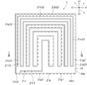
- FIG. 2 is a schematic plan view seen from the back side of the solar cell in the first embodiment.
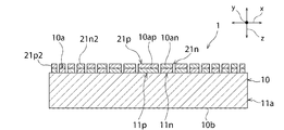
- FIG. 3 is a schematic cross-sectional view taken along line III-III in FIG.
- FIG. 4 is a schematic plan view of the solar cell string in the first embodiment.
- FIG. 5 is a schematic plan view of the solar cell in the second embodiment.
- FIG. 6 is a schematic plan view of a solar cell in the third embodiment.
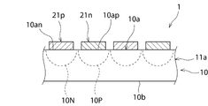
- FIG. 7 is a schematic cross-sectional view of a solar cell in the fourth embodiment.
- FIG. 1 is a schematic cross-sectional view of a solar cell module 3 according to the first embodiment.
- the solar cell module 3 includes a plurality of solar cell strings 2.
- Each of the plurality of solar cell strings 2 includes a plurality of solar cells 1 arranged along one direction (x direction).
- the plurality of solar cell strings 2 are arranged in parallel at predetermined intervals along another direction (y direction) orthogonal to one direction (x direction).
- the plurality of solar cells 1 are electrically connected by the wiring material 31.
- a plurality of solar cells 1 are electrically connected in series or in parallel by electrically connecting the electrodes of the solar cells 1 adjacent in the x direction by the wiring material 31.
- the wiring member 31 and the solar cell 1 are bonded by an adhesive layer (not shown) made of resin.
- the adhesive layer may be made of only a resin.
- the adhesive layer may have anisotropic conductivity including a resin layer and a conductive material dispersed in the resin layer.
- Specific examples of the conductive material include metal particles, alloy particles, and conductive materials having a minute size such as insulating particles coated with a metal or an alloy.
- the adhesive layer is made only of a resin adhesive, the wiring material 31 and the electrode of the solar cell 1 are bonded so as to be in direct contact.
- a first protective member 34 is disposed on the back side of the plurality of solar cells 1.
- a second protective member 35 is disposed on the light receiving surface side of the plurality of solar cells 1.
- a sealing material 33 is provided between the solar cell 1 and the first protective member 34 and between the solar cell 1 and the second protective member 35. The plurality of solar cells 1 are sealed between the first protective member 34 and the second protective member 35 by the sealing material 33.
- the material of the sealing material 33 and the first and second protective members 34 and 35 is not particularly limited.
- the sealing material 33 can be formed of, for example, a resin such as ethylene / vinyl acetate copolymer (EVA) or polyvinyl butyral (PVB).
- EVA ethylene / vinyl acetate copolymer
- PVB polyvinyl butyral
- the first protective member 34 disposed on the back surface side can be constituted by, for example, a resin film in which a metal foil such as glass, a resin film, or an aluminum foil is interposed.
- the second protective member 35 disposed on the light receiving surface side can be formed of a light-transmitting plate such as light-transmitting glass or resin.
- the solar cell module 3 is made of a metal such as Al attached to the outer periphery of a laminate having a first protective member 34, a sealing material 33, a plurality of solar cells 1, a sealing material 33, and a second protective member 35.
- a frame (not shown) may be provided.
- the solar cell module 3 may include a terminal box provided on the surface of the first protection member 34 for taking out the output of the solar cell 1 to the outside.
- FIG. 2 is a schematic plan view seen from the back side of the solar cell 1 in the first embodiment.
- FIG. 3 is a schematic cross-sectional view taken along line III-III in FIG.
- the solar cell 1 is a so-called back junction type solar cell.
- the solar cell 1 has a solar cell substrate 10.
- the solar cell substrate 10 is a member that generates carriers such as electrons and holes by receiving light.
- the solar cell substrate 10 has a light receiving surface 10b and a back surface 10a.
- the n-type surface 10an and the p-type surface 10ap are exposed on the back surface 10a.
- a passivation layer or an AR coating layer may be provided on the light receiving surface 10b.
- a light shielding material such as metal is not provided on the light receiving surface 10b. Therefore, in the solar cell 1 according to the present embodiment, light is incident on substantially the entire surface or the entire surface of the light receiving surface 10b.
- Each of the light-receiving surface 10b and the back surface 10a is rectangular.
- the “rectangle” includes a rectangle in which at least one of the four corners is chamfered or R-chamfered.
- the solar cell substrate 10 includes a substrate 11a, a p-type amorphous semiconductor layer 11p, and an n-type amorphous semiconductor layer 11n.
- the substrate 11a is made of a crystalline semiconductor having one conductivity type.
- the substrate 11a is configured by an n-type single crystal silicon substrate. For this reason, in this embodiment, a hole becomes a minority carrier.
- Each of the p-type amorphous semiconductor layer 11p and the n-type amorphous semiconductor layer 11n is disposed on the back surface of the substrate 11a.
- the p-type surface 10ap is constituted by the surface of the p-type amorphous semiconductor layer 11p.
- the n-type surface 10an is constituted by the surface of the n-type amorphous semiconductor layer 11n.
- the p-type amorphous semiconductor layer 11p can be composed of, for example, p-type amorphous silicon containing hydrogen.
- the n-type amorphous semiconductor layer 11n can be made of, for example, n-type amorphous silicon containing hydrogen.
- the solar cell substrate 10 is disposed between each of the p-type amorphous semiconductor layer 11p and the n-type amorphous semiconductor layer 11n and the substrate 11a so as not to substantially contribute to power generation (for example, several An i-type amorphous semiconductor layer ( ⁇ ⁇ 250 ⁇ ) may be further provided.
- the i-type amorphous semiconductor layer can be made of, for example, i-type amorphous silicon containing hydrogen.
- the junction characteristics between each of the p-type amorphous semiconductor layer 11p and the n-type amorphous semiconductor layer 11n and the substrate 11a can be improved.
- a solar cell having improved photoelectric conversion efficiency is provided.
- a p-side electrode 21p and an n-side electrode 21n are disposed on the back surface 10a of the solar cell substrate 10.
- the p-side electrode 21p is disposed on the p-type surface 10ap.
- the n-side electrode 21n is disposed on the n-type surface 10an.
- the substrate 11a is composed of an n-type single crystal silicon substrate, holes become minority carriers and electrons become majority carriers. Therefore, the p-side electrode 21p collects minority carriers, and the n-side electrode 21n collects majority carriers.
- the material of the p-side electrode 21p and the n-side electrode 21n is not particularly limited as long as it is a conductive material.
- Each of the p-side electrode 21p and the n-side electrode 21n is, for example, a metal such as silver, copper, aluminum, titanium, nickel, or chromium, an alloy containing one or more of these metals, TCO (Transparent Conductive Oxide), etc. Can be formed.
- each of the p-side electrode 21p and the n-side electrode 21n may be configured by a stacked body of a plurality of conductive layers made of, for example, the above metal, alloy, or TCO.
- Each of the p-side electrode 21p and the n-side electrode 21n can be formed by using various methods such as sputtering, vapor deposition, screen printing, or plating.
- the p-side electrode 21p includes a p-side bus bar portion 21p1, a plurality of p-side finger portions 21p2, and a p-side finger portion 21p3.
- the n-side electrode 21n includes an n-side bus bar portion 21n1 including a pad portion 21n3 and a plurality of n-side finger portions 21n2.
- the p-side bus bar portion 21p1 has a linear shape extending along the x direction (one direction) that is the direction in which the side 10a1 of the back surface 10a extends.
- the p-side bus bar portion 21p1 is provided with its area shifted to one side (x1 side) in the x direction of the back surface 10a.
- Each of the plurality of p-side finger portions 21p2 extends continuously from the p-side bus bar portion 21p1.
- the predetermined p-side finger portion 21p2 has a proximal end portion 21p21, a connection portion 21p22, and a distal end portion 21p23.
- all the finger portions excluding the finger portions located in the central portion in the x direction are composed of the base end portion 21p21 and the connection portion 21p22. And a tip 21p23.
- These bus bar portions are connected to the p-side bus bar portion 21p1 at the base end portion 21p21.
- the proximal end portion 21p21 extends along the y direction perpendicular to the x direction.
- the connection portion 21p22 connects the base end portion 21p21 and the tip end portion 21p23.
- the connection part 21p22 includes a bent part or a curved part. Specifically, in the present embodiment, the connection portion 21p22 includes a bent portion.
- the tip portion 21p23 extends along the y direction. The tip portion 21p23 faces the n-side bus bar portion 21n1 in the y direction. That is, the plurality of p-side electrodes 21p include U-shaped finger portions. In this embodiment, the finger part located in the center part of the x direction among several p side finger parts 21p2 is linear.
- the plurality of p-side finger portions 21p2 include a relatively long p-side finger portion and a relatively short p-side finger portion.
- the relatively long p-side finger portion is thinner than the relatively short p-side finger portion.
- the p-side finger portion located on the outer side is longer and thinner, and the p-side finger portion located on the inner side is shorter and thicker.
- the p-side finger portion 21p3 is electrically connected to the p-side bus bar portion 21p1.
- the p-side finger portion 21p3 extends to the x2 side from the tip end portion on the x2 side of the p-side bus bar portion 21p1.
- the p-side bus bar portion 21p1 is offset from one side (x1 side) in the x direction of the back surface 10a, and the p-side finger portion 21p3 extends to the other side (x2 side).
- the p-side finger portion 21p3 has a portion adjacent to the n-side bus bar portion 21n1 in the y direction.
- substantially the entire p-side finger portion 21p3 is adjacent to the n-side bus bar portion 21n1 in the y direction.
- the p-side finger portion 21p3 is located closer to the end side of the back surface 10a than the n-side bus bar portion 21n1 in the y direction.
- the n-side bus bar portion 21n1 has a linear shape extending along the x direction.
- the n-side bus bar portion 21n1 is provided with its area shifted to the other side (x2 side) in the x direction of the back surface 10a.
- the n-side bus bar portion 21n1 and the p-side bus bar portion 21p1 are arranged along the x direction. Specifically, the n-side bus bar portion 21n1 and the p-side bus bar portion 21p1 are arranged along the side 10a1 extending in the x direction.
- the width of the n-side bus bar portion 21n1 along the y direction is smaller than the width of the p-side bus bar portion 21p1 along the y direction.
- the n-side bus bar portion 21n1 and the p-side bus bar portion 21p1 each include a portion arranged linearly along the x direction.
- Each of the plurality of n-side finger portions 21n2 extends from the n-side bus bar portion 21n1.
- the plurality of n-side finger portions 21n2 are interleaved with the plurality of p-side finger portions 21p2.
- the plurality of n-side finger portions 21n2 include a base end portion 21n21, a connection portion 21n22, and a tip end portion 21n23.
- all n-side finger portions 21n2 have a base end portion 21n21, a connection portion 21n22, and a tip end portion 21n23.
- the n-side finger portion 21n2 is connected to the n-side bus bar portion 21n1 at the base end portion 21n21.
- the base end 21n21 extends along the y direction.
- the connection portion 21n22 connects the base end portion 21n21 and the distal end portion 21n23.
- the connection part 21n22 includes a bent part or a curved part. Specifically, in the present embodiment, the connection portion 21n22 includes a bent portion.
- the tip portion 21n23 extends along the y direction. The tip portion 21n23 faces the p-side bus bar portion 21p1 in the y direction. That is, the plurality of n-side electrodes 21n include U-shaped finger portions.
- the plurality of n-side finger portions 21n2 include a relatively long n-side finger portion and a relatively short n-side finger portion.
- the relatively long n-side finger portion is thinner than the relatively short n-side finger portion.
- the n-side finger portion positioned on the outer side is longer and thinner, and the n-side finger portion positioned on the inner side is shorter and thicker.
- a rectangular pad portion 21n3 is provided at the tip end portion on the x2 side of the n-side bus bar portion 21n1.
- the width along the y direction of the pad portion 21n3 is larger than the width along the y direction of the portion other than the pad portion 21n3 of the n-side bus bar portion 21n1.
- the n-side electrode 21 is electrically connected to the wiring material at the pad portion 21n3.
- FIG. 4 is a schematic plan view of the solar cell string 2 in the first embodiment.
- the plurality of solar cells 1 are arranged along the x direction so that the p-side bus bar portion 21p1 and the n-side bus bar portion 21n1 of the adjacent solar cells 1 are adjacent in the x direction. .
- the p-side bus bar portion 21p1 and the n-side bus bar portion 21n1 of the adjacent solar cells 1 are electrically connected by the wiring material 31.
- the wiring member 31 is connected by an adhesive layer (not shown) so as to include the tip end portion on the x1 side of the p-side bus bar portion 21p1 and the tip end portion on the x2 side of the n-side bus bar portion 21n1.
- the wiring member 31 is connected to the tip end portion on the x1 side of the p-side bus bar portion 21p1 and the pad portion 21n3 provided at the tip end portion on the x2 side of the n-side bus bar portion 21n1.
- carriers such as holes and electrons generated in the substrate 11a must move in the substrate 11a before being collected by the electrodes 21n and 21p.
- the carrier moves, loss due to carrier recombination is accompanied.
- the longer the movement distance of the carrier in the substrate 11a the more disappearance occurs due to the recombination of carriers.
- the photoelectric conversion efficiency of the solar cell is lowered accordingly.
- the bus bar portions 21p1, 21n1 are thicker than the finger portions 21p2, 21n2. For this reason, the carriers generated in the portions located below the bus bar portions 21p1 and 21n1 of the substrate 11a are generated by the electrodes 21p and 21n rather than the carriers generated in the portions located below the finger portions 21p2 and 21n2. Must travel long distances before being collected. Therefore, the longer the bus bar portion is, and the larger the occupied area of the bus bar portion on the back surface, the easier the carrier disappears.
- the n-side bus bar portion 21n1 and the p-side bus bar portion 21p1 extending in the x direction are arranged along the x direction.
- the p-side bus bar portions 21p1 and n on the back surface 10a are arranged more than when the p-side bus bar portion is arranged along one side of the back surface and the n-side bus bar portion is arranged along the other side facing the one side.
- the occupation ratio of the side bus bar portion 21n1 can be reduced. Therefore, disappearance due to carrier recombination can be suppressed. Therefore, improved photoelectric conversion efficiency can be realized.
- each of the plurality of p-side finger portions 21p2 and the plurality of n-side finger portions 21n2 has connection portions 21p22 and 21n22 including bent portions, and includes finger portions that are U-shaped. .
- the average length of the plurality of p-side finger portions 21p2 and the average length of the plurality of n-side finger portions 21n2 are larger than when the n-side bus bar portion and the p-side bus bar portion are arranged along the y direction. Can be long. Therefore, the average value of the area per finger part 21p2, 21n2 can be increased. Therefore, the number of finger portions 21p2 and 21n2 can be reduced.
- the length of the bus bar portions 21p1 and 21n1 can be further shortened. Therefore, the occupation ratio of the p-side bus bar portion 21p1 and the n-side bus bar portion 21n1 on the back surface 10a can be further reduced. Therefore, more improved photoelectric conversion efficiency can be realized.
- the p-side electrode 21p that collects holes that are minority carriers is a finger portion 21p3 that is adjacent to the n-side busbar portion 21n1 of the n-side electrode 21n that collects electrons that are majority carriers in the y direction.
- substrates 11a and the p side electrode 21p can be shortened. Therefore, minority carriers (holes) generated in a portion of the substrate 11a located below the y2 side portion of the n-side bus bar portion 21n1 can be efficiently collected in the finger portion 21p3. Therefore, further improved photoelectric conversion efficiency can be realized.
- the n-side bus bar portion 21n1 and the p-side bus bar portion 21p1 are arranged along the x direction. For this reason, as shown in FIG. 4, adjacent solar cells 1 can be easily connected by a short and thin wiring material 31. That is, the adhesion area between the wiring member 31 and the solar cell 1 can be reduced. Moreover, the length along the x direction of the part adhering to the wiring material 31 of the solar cell 1 can be shortened. Therefore, the size of the constrained portion of the solar cell 1 by the wiring material 31 can be reduced. Therefore, for example, even when the temperature of the solar cell module 3 changes and a difference in thermal expansion coefficient occurs between the wiring member 31 and the solar cell 1, the solar cell 1 is hardly warped. Moreover, the wiring material 31 is difficult to peel from the solar cell 1. Therefore, the solar cell module 3 having improved reliability can be realized.
- the finger portions 21p2 and 21n2 include a relatively long finger portion and a relatively short finger portion. And a relatively long finger part is thinner than a relatively short finger part.
- the finger part located on the outer side is longer and thinner, and the finger part located on the inner side is shorter and thicker. For this reason, the difference of the area of a relatively long finger part and the area of a relatively short finger part can be made small. Therefore, for example, when the p-side electrode 21p and the n-side electrode 21n are formed by plating, the difference between the thickness of the relatively long finger portion and the thickness of the relatively short finger portion can be reduced. That is, the p-side electrode 21p and the n-side electrode 21n with small thickness unevenness can be formed by plating.
- FIGS. 1 and 4 are referred to in common with the first embodiment.
- FIG. 5 is a schematic plan view of the solar cell in the second embodiment.
- the finger portions 21p2 and 21n2 include a relatively long finger portion and a relatively short finger portion, and the relatively long finger portion is a relatively short finger.
- An example thinner than the above has been described.
- the present invention is not limited to this configuration.
- the relatively long finger part is thicker than the relatively short finger part.
- the finger portions 21p2 and 21n2 the finger portions located on the outer side are longer and thicker, and the finger portions located on the inner side are shorter and thinner.
- the resistance loss in the long finger part can be reduced by increasing the thickness of the long finger part in which many carriers are collected. Therefore, further improved photoelectric conversion efficiency can be realized.
- FIG. 6 is a schematic plan view of a solar cell in the third embodiment.
- the p-side bus bar portion 21p1 and the n-side bus bar portion 21n1 are arranged along the side 10a1.
- the p-side bus bar portion 21p1 and the n-side bus bar portion 21n1 are arranged along the x direction at the central portion in the y direction of the back surface 10a.
- the plurality of p-side bus bar portions 21p1 include a finger portion whose base end portion extends from the p-side bus bar portion 21p1 to the y1 side and a finger portion whose base end portion extends from the p-side bus bar portion 21p1 to the y2 side. ing. That is, the p-side finger portion 21p2 extends from the p-side bus bar portion 21p1 to both sides in the y direction.
- the plurality of n-side bus bar portions 21n1 include a finger portion whose base end portion extends from the n-side bus bar portion 21n1 to the y1 side, and a finger portion whose base end portion extends from the n-side bus bar portion 21n1 to the y2 side. . That is, the n-side finger portion 21n2 extends from the n-side bus bar portion 21n1 to both sides in the y direction.
- the finger portion 21p3 is disposed in the recess 21n11 provided in the n-side bus bar portion 21n1.
- FIG. 7 is a schematic cross-sectional view of a solar cell in the fourth embodiment.
- the present invention is not limited to this configuration.
- the solar cell substrate 10 has one conductivity type, and a p-type dopant diffusion region 10P in which a p-type dopant is diffused and an n-type dopant diffusion region 10N in which an n-type dopant is diffused are provided on the back surface side.
- the substrate 11a is formed.
- the p-type surface 10ap is constituted by the surface of the p-type dopant diffusion region 10P.
- the n-type surface 10an is constituted by the surface of the n-type dopant diffusion region 10N.
- the present invention includes various embodiments that are not described here.
- the example in which the widths of the relatively long finger portions and the relatively short finger portions are different has been described, but the present invention is not limited to this.
- the present invention includes a case where the widths of the relatively long finger portions and the relatively short finger portions are approximately the same.
- the p-side bus bar portion and the n-side bus bar portion are described as an example in which one set is arranged along the x direction at the center portion in the y direction on the back surface.
- a plurality of sets of p-side bus bar portions and n-side bus bar portions may be arranged along the x direction.
- at least one or more sets of p-side bus bar portions and n-side bus bar portions are provided in the central portion other than the end portions in the y-direction on the back surface, a set of some bus bars in the y-direction. It may be at the end.
Landscapes
- Photovoltaic Devices (AREA)
Abstract
改善された光電変換効率を有する太陽電池を提供する。 太陽電池1は、一主面10aにn型表面10anとp型表面10apとを含む太陽電池基板10と、n型表面10anの上に配されているn側電極21nと、p型表面10apの上に配されているp側電極21pとを備えている。p側電極21pは、第1の方向xに沿って延びるp側バスバー部21p1と、p側バスバー部21p1から延びる複数のp側フィンガー部21p2とを有する。n側電極は、第1の方向xに沿って延びるn側バスバー部21n1と、n側バスバー部21n1から延びる複数のn側フィンガー部21n2とを有する。n側バスバー部21n1と、p側バスバー部21p1とは、第1の方向xに沿って配列されている。
Description
本発明は、裏面接合型の太陽電池及びそれを備える太陽電池モジュールに関する。
従来、例えば下記の特許文献1などにおいて、太陽電池の裏面側にp型及びn型の半導体領域が配されている所謂裏面接合型の太陽電池が提案されている。この裏面接合型の太陽電池では、受光面側に電極を設ける必要がない。このため、裏面接合型の太陽電池では、光の受光効率を高めることができる。従って、より高い光電変換効率を実現し得る。
近年、太陽電池に対する光電変換効率向上の要求がさらに高まってきている。
本発明は、斯かる点に鑑みて成されたものであり、その目的は、改善された光電変換効率を有する太陽電池を提供することにある。
本発明に係る太陽電池は、太陽電池基板と、n側電極と、p側電極とを備えている。太陽電池基板は、一主面にn型表面とp型表面とを含む。n側電極は、n型表面の上に配されている。p側電極は、p型表面の上に配されている。p側電極は、p側バスバー部と、複数のp側フィンガー部とを有する。p側バスバー部は、第1の方向に沿って延びている。複数のp側フィンガー部は、p側バスバー部から延びている。n側電極は、n側バスバー部と、複数のn側フィンガー部とを有する。n側バスバー部は、第1の方向に沿って延びている。複数のn側フィンガー部は、n側バスバー部から延びている。複数のn側フィンガー部は、複数のp側フィンガー部と間挿し合っている。n側バスバー部と、p側バスバー部とは、第1の方向に沿って配列されている。
本発明に係る太陽電池モジュールは、複数の太陽電池と、配線材とを備えている。配線材は、複数の太陽電池を電気的に接続している。太陽電池は、太陽電池基板と、n側電極と、p側電極とを備えている。太陽電池基板は、一主面にn型表面とp型表面とを含む。n側電極は、n型表面の上に配されている。p側電極は、p型表面の上に配されている。p側電極は、p側バスバー部と、複数のp側フィンガー部とを有する。p側バスバー部は、第1の方向に沿って延びている。複数のp側フィンガー部は、p側バスバー部から延びている。n側電極は、n側バスバー部と、複数のn側フィンガー部とを有する。n側バスバー部は、第1の方向に沿って延びている。複数のn側フィンガー部は、n側バスバー部から延びている。複数のn側フィンガー部は、複数のp側フィンガー部と間挿し合っている。n側バスバー部と、p側バスバー部とは、第1の方向に沿って配列されている。
本発明によれば、改善された光電変換効率を有する太陽電池を提供することができる。
以下、本発明を実施した好ましい形態の一例について説明する。但し、以下の実施形態は、単なる例示である。本発明は、以下の実施形態に何ら限定されない。
また、実施形態等において参照する各図面において、実質的に同一の機能を有する部材は同一の符号で参照することとする。また、実施形態等において参照する図面は、模式的に記載されたものであり、図面に描画された物体の寸法の比率などは、現実の物体の寸法の比率などとは異なる場合がある。図面相互間においても、物体の寸法比率等が異なる場合がある。具体的な物体の寸法比率等は、以下の説明を参酌して判断されるべきである。
(第1の実施形態)
図1は、第1の実施形態に係る太陽電池モジュール3の略図的断面図である。太陽電池モジュール3は、複数の太陽電池ストリング2を備えている。複数の太陽電池ストリング2のそれぞれは、一の方向(x方向)に沿って配列された複数の太陽電池1を備えている。複数の太陽電池ストリング2は、一の方向(x方向)に直交する他の方向(y方向)に沿って、所定の間隔を隔てて並列配置されている。複数の太陽電池1は、配線材31によって電気的に接続されている。具体的には、x方向に隣り合う太陽電池1の電極が配線材31によって電気的に接続されることによって、複数の太陽電池1が直列または並列に電気的に接続されている。
図1は、第1の実施形態に係る太陽電池モジュール3の略図的断面図である。太陽電池モジュール3は、複数の太陽電池ストリング2を備えている。複数の太陽電池ストリング2のそれぞれは、一の方向(x方向)に沿って配列された複数の太陽電池1を備えている。複数の太陽電池ストリング2は、一の方向(x方向)に直交する他の方向(y方向)に沿って、所定の間隔を隔てて並列配置されている。複数の太陽電池1は、配線材31によって電気的に接続されている。具体的には、x方向に隣り合う太陽電池1の電極が配線材31によって電気的に接続されることによって、複数の太陽電池1が直列または並列に電気的に接続されている。
配線材31と太陽電池1とは、樹脂からなる接着剤層(図示せず)により接着されている。接着剤層は、樹脂のみからなるものであってもよい。また、接着剤層は、樹脂層と、その樹脂層中に分散した導電材とを含む異方導電性を有するものであってもよい。導電材の具体例としては、金属粒子や、合金粒子、金属または合金によりコーティングされた絶縁性粒子等の微小なサイズの導電材が挙げられる。なお、接着剤層が樹脂接着剤のみからなる場合は、配線材31と太陽電池1の電極とが直接接触するように接着を行う。
複数の太陽電池1の裏面側には、第1の保護部材34が配置されている。一方、複数の太陽電池1の受光面側には、第2の保護部材35が配置されている。太陽電池1と第1の保護部材34との間及び太陽電池1と第2の保護部材35との間には、封止材33が設けられている。複数の太陽電池1は、この封止材33により、第1の保護部材34と第2の保護部材35との間に封止されている。
封止材33並びに第1及び第2の保護部材34,35の材料は、特に限定されない。封止材33は、例えば、エチレン・酢酸ビニル共重合体(EVA)やポリビニルブチラール(PVB)等の樹脂により形成することができる。
裏面側に配された第1の保護部材34は、例えば、ガラス、樹脂フィルムやアルミニウム箔などの金属箔を介在させた樹脂フィルムにより構成することができる。
受光面側に配された第2の保護部材35は、例えば、透光性のガラスや樹脂等の透光性を有する板体により構成することができる。
太陽電池モジュール3は、第1の保護部材34、封止材33、複数の太陽電池1、封止材33、第2の保護部材35を有する積層体の外周に取り付けられたAl等の金属製の枠体(図示しない)を備えていてもよい。また、太陽電池モジュール3は、第1の保護部材34の表面に設けられた、太陽電池1の出力を外部に取り出すための端子ボックスを備えていてもよい。
図2は、第1の実施形態における太陽電池1の裏面側からみた略図的平面図である。図3は、図2の線III-IIIにおける略図的断面図である。
太陽電池1は、所謂裏面接合型の太陽電池である。太陽電池1は、太陽電池基板10を有する。太陽電池基板10は、受光することによって電子や正孔などのキャリアを生成させる部材である。太陽電池基板10は、受光面10bと、裏面10aとを有する。裏面10aには、n型表面10anと、p型表面10apとが露出している。受光面10b上には、パッシベーション層やARコート層が設けられていてもよい。受光面10b上には、金属等の遮光材が設けられていない。よって、本実施形態に係る太陽電池1は、受光面10bの略全面または全面に光が入射する。
受光面10b及び裏面10aのそれぞれは、矩形状である。ここで、「矩形」には、4つの角部の少なくともひとつが面取り状またはR面取り状である矩形が含まれるものとする。
本実施形態においては、太陽電池基板10は、基板11aと、p型非晶質半導体層11pと、n型非晶質半導体層11nとを備えている。基板11aは、一の導電型を有する結晶性半導体からなる。具体的には、本実施形態では、基板11aは、n型単結晶シリコン基板により構成されている。このため、本実施形態では、正孔が少数キャリアとなる。
p型非晶質半導体層11p及びn型非晶質半導体層11nのそれぞれは、基板11aの裏面の上に配されている。p型表面10apは、p型非晶質半導体層11pの表面により構成される。n型表面10anは、n型非晶質半導体層11nの表面により構成されている。
p型非晶質半導体層11pは、例えば、水素を含むp型のアモルファスシリコンにより構成することができる。n型非晶質半導体層11nは、例えば、水素を含むn型のアモルファスシリコンにより構成することができる。太陽電池基板10は、p型非晶質半導体層11p及びn型非晶質半導体層11nのそれぞれと、基板11aとの間に配された、発電に実質的に寄与しない程度の厚み(例えば数Å~250Å)のi型非晶質半導体層をさらに備えていてもよい。その場合、i型非晶質半導体層は、例えば、水素を含むi型のアモルファスシリコンにより構成することができる。i型非晶質半導体層を設けることで、p型非晶質半導体層11p及びn型非晶質半導体層11nのそれぞれと、基板11aとの間の接合特性を改善することができ、より改善された光電変換効率を有する太陽電池が提供される。
太陽電池基板10の裏面10aの上には、p側電極21pとn側電極21nとが配されている。p側電極21pは、p型表面10apの上に配されている。n側電極21nは、n型表面10anの上に配されている。本実施形態においては、基板11aがn型単結晶シリコン基板により構成されているので、正孔が少数キャリアとなり、電子が多数キャリアとなる。従って、p側電極21pは少数キャリアを収集し、n側電極21nは多数キャリアを収集する。
p側電極21p及びn側電極21nの材質は、導電材料である限りにおいて特に限定されない。p側電極21p及びn側電極21nのそれぞれは、例えば、銀、銅、アルミニウム、チタン、ニッケル、クロムなどの金属や、それらの金属のうちの一種以上を含む合金、TCO(Transparent Conductive Oxide)などにより形成することができる。また、p側電極21p及びn側電極21nのそれぞれは、例えば、上記金属や合金、TCOからなる複数の導電層の積層体により構成されていてもよい。
p側電極21p及びn側電極21nのそれぞれは、例えば、スパッタ法、蒸着法、スクリーン印刷法或いはメッキ法等の種々の方法を用いて形成することができる。
p側電極21pは、p側バスバー部21p1と、複数のp側フィンガー部21p2と、p側フィンガー部21p3とを有する。n側電極21nは、パッド部21n3を含むn側バスバー部21n1と、複数のn側フィンガー部21n2とを有する。
p側バスバー部21p1は、裏面10aの辺10a1の延びる方向であるx方向(一の方向)に沿って延びる線状の形状を有する。p側バスバー部21p1は、裏面10aのx方向の一方の側(x1側)に面積を片寄らせて設けられている。
複数のp側フィンガー部21p2のそれぞれは、p側バスバー部21p1から連続して延びている。所定のp側フィンガー部21p2は、基端部21p21と、接続部21p22と、先端部21p23とを有する。本実施形態では、具体的には、複数のp側フィンガー部21p2のうち、x方向の中央部に位置しているフィンガー部を除いたすべてのフィンガー部が、基端部21p21と、接続部21p22と、先端部21p23とを有する。これらのバスバー部は、基端部21p21においてp側バスバー部21p1と接続されている。基端部21p21は、x方向に対して垂直なy方向に沿って延びている。接続部21p22は、基端部21p21と先端部21p23とを接続している。接続部21p22は、屈曲部または湾曲部を含んでいる。具体的には、本実施形態では、接続部21p22は、屈曲部を含んでいる。先端部21p23は、y方向に沿って延びている。先端部21p23は、n側バスバー部21n1とy方向に対向している。つまり、複数のp側電極21pは、U字状のフィンガー部を含む。本実施形態においては、複数のp側フィンガー部21p2のうち、x方向の中央部に位置しているフィンガー部は、直線状である。
複数のp側フィンガー部21p2には、相対的に長いp側フィンガー部と、相対的に短いp側フィンガー部とが含まれている。そして、相対的に長いp側フィンガー部は、相対的に短いp側フィンガー部よりも細い。具体的には、本実施形態では、複数のp側フィンガー部21p2のうち、外側に位置するp側フィンガー部ほど長く且つ細く、内側に位置するp側フィンガー部ほど短く且つ太い。
p側フィンガー部21p3は、p側バスバー部21p1に電気的に接続されている。p側フィンガー部21p3は、p側バスバー部21p1のx2側先端部から、x2側に延びている。p側バスバー部21p1は、裏面10aのx方向の一方の側(x1側)に片寄って設けられ、p側フィンガー部21p3は他方の側(x2側)に延びている。p側フィンガー部21p3は、y方向において、n側バスバー部21n1と隣り合う部分を有する。具体的には、本実施形態では、p側フィンガー部21p3の実質的に全体が、y方向において、n側バスバー部21n1と隣り合っている。またp側フィンガー部21p3は、y方向において、n側バスバー部21n1よりも裏面10aの端側に位置する。
n側バスバー部21n1は、x方向に沿って延びる線状の形状を有する。n側バスバー部21n1は、裏面10aのx方向の他方の側(x2側)に面積を片寄らせて設けられている。n側バスバー部21n1とp側バスバー部21p1とは、x方向に沿って配列されている。具体的には、n側バスバー部21n1とp側バスバー部21p1とは、x方向に延びる辺10a1に沿って配列されている。n側バスバー部21n1のy方向に沿った幅は、p側バスバー部21p1のy方向に沿った幅よりも小さい。n側バスバー部21n1とp側バスバー部21p1とは、夫々x方向に沿って直線状に配列された部分を含む。
複数のn側フィンガー部21n2のそれぞれは、n側バスバー部21n1から延びている。複数のn側フィンガー部21n2は、複数のp側フィンガー部21p2と間挿し合っている。複数のn側フィンガー部21n2は、基端部21n21と、接続部21n22と、先端部21n23とを有する。具体的には、本実施形態では、すべてのn側フィンガー部21n2が、基端部21n21と、接続部21n22と、先端部21n23とを有する。n側フィンガー部21n2は、基端部21n21においてn側バスバー部21n1と接続されている。基端部21n21は、y方向に沿って延びている。接続部21n22は、基端部21n21と先端部21n23とを接続している。接続部21n22は、屈曲部または湾曲部を含む。具体的には、本実施形態では、接続部21n22は、屈曲部を含む。先端部21n23は、y方向に沿って延びている。先端部21n23は、p側バスバー部21p1とy方向に対向している。つまり、複数のn側電極21nは、U字状のフィンガー部を含む。
複数のn側フィンガー部21n2には、相対的に長いn側フィンガー部と、相対的に短いn側フィンガー部とが含まれている。そして、相対的に長いn側フィンガー部は、相対的に短いn側フィンガー部よりも細い。具体的には、本実施形態では、複数のn側フィンガー部21n2のうち、外側に位置するn側フィンガー部ほど長く且つ細く、内側に位置するn側フィンガー部ほど短く且つ太い。
n側バスバー部21n1のx2側先端部には、矩形状のパッド部21n3が設けられている。パッド部21n3のy方向に沿った幅は、n側バスバー部21n1のパッド部21n3以外の部分のy方向に沿った幅よりも大きい。本実施形態では、n側電極21は、このパッド部21n3において配線材と電気的に接続されている。
図4は、第1の実施形態における太陽電池ストリング2の略図的平面図である。太陽電池ストリング2において、複数の太陽電池1は、隣り合う太陽電池1のp側バスバー部21p1と、n側バスバー部21n1とがx方向において隣り合うように、x方向に沿って配列されている。隣り合う太陽電池1のp側バスバー部21p1とn側バスバー部21n1とは、配線材31によって電気的に接続されている。配線材31は、図示しない接着剤層により、p側バスバー部21p1のx1側の先端部と、n側バスバー部21n1のx2側先端部とを含むように接続されている。図4では、配線材31は、p側バスバー部21p1のx1側の先端部と、n側バスバー部21n1のx2側先端部に設けられたパッド部21n3とに接続されている。
ところで、基板11aにおいて生じた正孔や電子などのキャリアは、電極21n、21pに収集されるまでに基板11a内を移動しなければならない。但し、キャリアの移動に際しては、キャリアの再結合による消失が伴う。このため、キャリアの基板11a内における移動距離が長いほど、キャリアの再結合による消失がより多く発生することとなる。キャリアの消失が生じると、その分だけ、太陽電池の光電変換効率が低下することとなる。特に、少数キャリア(本実施形態においては、ホール)の再結合が多くなるほど、太陽電池の光電変換効率が大きく低下する。
ここで、バスバー部21p1,21n1は、フィンガー部21p2,21n2に対して太い。このため、基板11aのバスバー部21p1,21n1の下方に位置している部分において生成したキャリアは、フィンガー部21p2,21n2の下方に位置している部分において生成したキャリアよりも、電極21p、21nにより収集されるまでに長い距離を移動しなければならない。よって、バスバー部が長く、裏面におけるバスバー部の占有面積が大きくなるほどキャリアの消失が生じやすくなる。
ここで、本実施形態では、x方向に延びるn側バスバー部21n1とp側バスバー部21p1とがx方向に沿って配列されている。このため、例えば、裏面の一辺に沿ってp側バスバー部を配置し、その一辺に対向する他辺に沿ってn側バスバー部を配置した場合よりも、裏面10aにおけるp側バスバー部21p1及びn側バスバー部21n1の占有率を低くすることができる。よって、キャリアの再結合による消失を抑制することができる。従って、改善された光電変換効率を実現することができる。
特に、本実施形態では、複数のp側フィンガー部21p2及び複数のn側フィンガー部21n2のそれぞれは、屈曲部を含む接続部21p22、21n22を有しており、U字状であるフィンガー部を含む。このため、例えば、y方向に沿ってn側バスバー部とp側バスバー部とを配列した場合よりも複数のp側フィンガー部21p2の平均長さ及び複数のn側フィンガー部21n2の平均長さを長くすることができる。よって、フィンガー部21p2,21n2の1本あたりの面積の平均値を大きくすることができる。従って、フィンガー部21p2,21n2の本数を少なくすることができる。ここで、バスバー部は、接続すべきフィンガー部の本数が多くなるほど長くする必要がある。従って、フィンガー部21p2,21n2の本数を少なくすることができる本実施形態においては、バスバー部21p1,21n1の長さをより短くすることができる。よって、裏面10aにおけるp側バスバー部21p1及びn側バスバー部21n1の占有率をより低くすることができる。従って、より改善された光電変換効率を実現することができる。
さらには、本実施形態においては、少数キャリアであるホールを収集するp側電極21pは、多数キャリアである電子を収集するn側電極21nのn側バスバー部21n1とy方向に隣り合うフィンガー部21p3を有する。このため、基板11aのうち、n側バスバー部21n1のy2側部分の下方に位置している部分と、p側電極21pとの間の距離を短くすることができる。よって、基板11aのうち、n側バスバー部21n1のy2側部分の下方に位置している部分において発生した少数キャリア(ホール)をフィンガー部21p3において効率的に収集することができる。従って、さらに改善された光電変換効率を実現することができる。
本実施形態では、上述のように、n側バスバー部21n1とp側バスバー部21p1とがx方向に沿って配列されている。このため、図4に示すように、隣り合う太陽電池1同士を、短く且つ細い配線材31によって容易に接続することができる。すなわち、配線材31と太陽電池1との接着面積を小さくできる。また、太陽電池1の配線材31と接着している部分のx方向に沿った長さを短くすることができる。よって、配線材31による太陽電池1の拘束部分の大きさを小さくすることができる。従って、例えば太陽電池モジュール3の温度が変化し、配線材31と太陽電池1との間に熱膨張率差が生じた場合であっても、太陽電池1に反りが発生し難い。また、配線材31が太陽電池1から剥離しにくい。従って、改善された信頼性を有する太陽電池モジュール3を実現することができる。
また、本実施形態では、フィンガー部21p2,21n2には、相対的に長いフィンガー部と、相対的に短いフィンガー部とが含まれている。そして、相対的に長いフィンガー部は、相対的に短いフィンガー部よりも細い。具体的には、本実施形態では、フィンガー部21p2,21n2のうち、外側に位置するフィンガー部ほど長く且つ細く、内側に位置するフィンガー部ほど短く且つ太い。このため、相対的に長いフィンガー部の面積と、相対的に短いフィンガー部の面積との差を小さくできる。従って、例えば、p側電極21p及びn側電極21nをめっき法により形成した場合に、相対的に長いフィンガー部の厚みと相対的に短いフィンガー部の厚みとの差を小さくすることができる。すなわち、めっき法により、厚みむらの小さなp側電極21p及びn側電極21nを形成することができる。
以下、本発明を実施した好ましい形態の他の例について説明する。以下の説明において、上記第1の実施形態と実質的に共通の機能を有する部材を共通の符号で参照し、説明を省略する。
また、下記の第2及び第3の実施形態において、図1及び図4は、上記第1の実施形態と共通に参照する。
(第2の実施形態)
図5は、第2の実施形態における太陽電池の略図的平面図である。
図5は、第2の実施形態における太陽電池の略図的平面図である。
上記第1の実施形態では、フィンガー部21p2,21n2には、相対的に長いフィンガー部と、相対的に短いフィンガー部とが含まれており、相対的に長いフィンガー部は、相対的に短いフィンガー部よりも細い例について説明した。但し、本発明は、この構成に限定されない。
本実施形態では、相対的に長いフィンガー部は、相対的に短いフィンガー部よりも太い。具体的には、本実施形態では、フィンガー部21p2,21n2のうち、外側に位置するフィンガー部ほど長く且つ太く、内側に位置するフィンガー部ほど短く且つ細い。このように、多くのキャリアが収集される長いフィンガー部ほど太くすることによって、長いフィンガー部における抵抗ロスを低減することができる。従って、さらに改善された光電変換効率を実現することができる。
(第3の実施形態)
図6は、第3の実施形態における太陽電池の略図的平面図である。
図6は、第3の実施形態における太陽電池の略図的平面図である。
上記第1の実施形態では、p側バスバー部21p1とn側バスバー部21n1とが辺10a1に沿って配列されている例について説明した。それに対して、本実施形態では、p側バスバー部21p1とn側バスバー部21n1とは、裏面10aのy方向における中央部において、x方向に沿って配列されている。また、複数のp側バスバー部21p1には、基端部がp側バスバー部21p1からy1側に延びるフィンガー部と、基端部がp側バスバー部21p1からy2側に延びるフィンガー部とが含まれている。すなわち、p側バスバー部21p1から、y方向の両側にp側フィンガー部21p2が延びている。
複数のn側バスバー部21n1には、基端部がn側バスバー部21n1からy1側に延びるフィンガー部と、基端部がn側バスバー部21n1からy2側に延びるフィンガー部とが含まれている。すなわち、n側バスバー部21n1から、y方向の両側にn側フィンガー部21n2が延びている。
このようにすることにより、バスバー部21p1,21n1のy1側にのみフィンガー部21p2,21n2が接続されている第1の実施形態よりもバスバー部21p1,21n1の長さを短く保ったままで、フィンガー部21p2,21n2の本数を多くすることができる。その結果、フィンガー部21p2,21n2の長さを短くすることができ、抵抗ロスを低減することができる。従って、さらに改善された光電変換効率を実現することができる。
なお、本実施形態では、n側バスバー部21n1に設けられた凹部21n11内にフィンガー部21p3が配されている。
(第4の実施形態)
図7は、第4の実施形態における太陽電池の略図的断面図である。
図7は、第4の実施形態における太陽電池の略図的断面図である。
上記第1の実施形態では、太陽電池基板10が、半導体からなる基板11aと、半導体層11p、11nとを備えている例について説明した。但し、本発明は、この構成に限定されない。
本実施形態では、太陽電池基板10は、一の導電型を有し、裏面側に、p型ドーパントが拡散したp型ドーパント拡散領域10P及びn型ドーパントが拡散したn型ドーパント拡散領域10Nが設けられている基板11aにより構成されている。本実施形態では、p型表面10apは、p型ドーパント拡散領域10Pの表面により構成される。n型表面10anは、n型ドーパント拡散領域10Nの表面により構成されている。
斯かる構成においても、前述の実施形態と同様の効果を奏する。
尚、本発明はここでは記載していない様々な実施形態を含む。例えば、上述した第1及び第2の実施形態では相対的に長いフィンガー部と、相対的に短いフィンガー部との幅が異なる例について説明したが、本発明はこれに限定されない。本発明は、相対的に長いフィンガー部と、相対的に短いフィンガー部との幅が同程度の場合も含む。
また、第3の実施形態ではp側バスバー部とn側バスバー部とは、裏面のy方向における中央部において、x方向に沿って一組配列されている例について説明したが、これに限らず複数組のp側バスバー部とn側バスバー部とを、x方向に沿って配列するようにしても良い。この場合に、少なくとも1以上の組のp側バスバー部とn側バスバー部とを、裏面のy方向における端部以外の中央部に設けるようにすれば、一部のバスバーの組がy方向における端部にあっても良い。
以上のように、本発明はここでは記載していない様々な実施形態を含む。従って、本発明の技術的範囲は上記の説明から妥当な特許請求の範囲に係る発明特定事項によってのみ定められるものである。
1…太陽電池
3…太陽電池モジュール
10…太陽電池基板
10a…裏面
10a1…辺
10an…n型表面
10ap…p型表面
21n…n側電極
21n1…n側バスバー部
21n2…n側フィンガー部
21n22,21p22…接続部
21p…p側電極
21p1…p側バスバー部
21p2…p側フィンガー部
31…配線材
3…太陽電池モジュール
10…太陽電池基板
10a…裏面
10a1…辺
10an…n型表面
10ap…p型表面
21n…n側電極
21n1…n側バスバー部
21n2…n側フィンガー部
21n22,21p22…接続部
21p…p側電極
21p1…p側バスバー部
21p2…p側フィンガー部
31…配線材
Claims (19)
- 一主面にn型表面とp型表面とを含む太陽電池基板と、
前記n型表面の上に配されたn側電極と、
前記p型表面の上に配されたp側電極と、
を備え、
前記p側電極は、第1の方向に沿って延びるp側バスバー部と、前記p側バスバー部から延びる複数のp側フィンガー部とを有し、
前記n側電極は、前記第1の方向に沿って延びるn側バスバー部と、前記n側バスバー部から延び、前記複数のp側フィンガー部と間挿し合っている複数のn側フィンガー部とを有し、
前記n側バスバー部と、前記p側バスバー部とは、前記第1の方向に沿って配列されている、太陽電池。 - 前記太陽電池基板は矩形状の形状を有し、
前記第1の方向は、前記一主面の一辺が延びる方向である、請求項1に記載の太陽電池。 - 前記n側バスバー部は、前記第1の方向の一方の側に面積を片寄らせて配置され、前記p側バスバー部は、前記第1の方向の他方の側に面積を片寄らせて配置されている、請求項1または2記載の太陽電池。
- 前記n側バスバー部とp側バスバー部とは、夫々前記第1の方向に沿って直線状に配列された部分を含む、請求項1~3のいずれか一項に記載の太陽電池。
- n側バスバー部とp側バスバー部とのうち少数キャリア収集用の一方のバスバー部の面積は、多数キャリア収集用の他方のバスバー部の面積より大きい、請求項1~4のいずれか一項に記載の太陽電池。
- 前記複数のp側フィンガー部と前記複数のn側フィンガー部とのそれぞれは、屈曲部または湾曲部を有するフィンガー部を含む、請求項1~5のいずれか一項に記載の太陽電池。
- 前記複数のp側フィンガー部と前記複数のn側フィンガー部とのそれぞれは、
前記p側またはn側バスバー部から垂直に延びる基端部と、
前記屈曲部または前記湾曲部と、
前記屈曲部または前記湾曲部によって前記基端部に接続されており、前記n側またはp側バスバー部と対向している先端部と、
を有するフィンガー部を含む、請求項6に記載の太陽電池。 - 前記p側フィンガー部と前記n側フィンガー部とのそれぞれは、U字状のフィンガー部を含む、請求項1~7のいずれか一項に記載の太陽電池。
- 前記複数のp側フィンガー部と、前記複数のn側フィンガー部とのうちの少なくとも一方には、相対的に長いフィンガー部と、相対的に短いフィンガー部とが含まれ、前記相対的に長いフィンガー部の方が、前記相対的に短いフィンガー部よりも太い、請求項1~8のいずれか一項に記載の太陽電池。
- 前記複数のp側フィンガー部と、前記複数のn側フィンガー部とのうちの少なくとも一方には、相対的に長いフィンガー部と、相対的に短いフィンガー部とが含まれ、前記相対的に長いフィンガー部の方が、前記相対的に短いフィンガー部よりも細い、請求項1~8のいずれか一項に記載の太陽電池。
- 前記p側電極及び前記n側電極のうち、少数キャリアを収集する側の電極は、前記第1の方向に対して垂直な第2の方向において、多数キャリアを収集する側の電極のバスバー部と隣り合う部分を有する、請求項1~10のいずれか一項に記載の太陽電池。
- 前記p側バスバー部及び前記n側バスバー部は、前記一主面の一辺に沿って配列されている、請求項2~11のいずれか一項に記載の太陽電池。
- 前記複数のp側フィンガー部は、
基端部が、前記p側バスバー部から前記第1の方向に対して垂直な第2の方向の一方側に延びているフィンガー部と、
基端部が、前記p側バスバー部から前記第2の方向の他方側に延びているフィンガー部と、
を含み、
前記複数のn側フィンガー部は、
基端部が、前記n側バスバー部から前記第2の方向の一方側に延びているフィンガー部と、
基端部が、前記n側バスバー部から前記第2の方向の他方側に延びているフィンガー部と、
を含む、請求項1~12のいずれか一項に記載の太陽電池。 - 前記一主面の第2の方向における中央部に配されている前記p側バスバー部と前記n側バスバー部とを含む、請求項13に記載の太陽電池。
- 前記太陽電池基板の前記一主面と対向する他主面の略全面または全面が受光面となる、請求項1~14のいずれか一項に記載の太陽電池。
- 複数の太陽電池と、前記複数の太陽電池を電気的に接続している配線材とを備える太陽電池モジュールであって、
前記太陽電池は、
一主面にn型表面とp型表面とを含む太陽電池基板と、
前記n型表面の上に配されたn側電極と、
前記p型表面の上に配されたp側電極と、
を有し、
前記p側電極は、第1の方向に沿って延びるp側バスバー部と、前記p側バスバー部から延びる複数のp側フィンガー部とを有し、
前記n側電極は、前記第1の方向に沿って延びるn側バスバー部と、前記n側バスバー部から延び、前記複数のp側フィンガー部と間挿し合っている複数のn側フィンガー部とを有し、
前記n側バスバー部と、前記p側バスバー部とは、前記第1の方向に沿って配列されている、太陽電池モジュール。 - 前記太陽電池基板は矩形状の形状を有し、
前記第1の方向は、前記一主面の一辺が延びる方向である、請求項16に記載の太陽電池モジュール。 - 前記複数の太陽電池は、隣り合う太陽電池の前記p側バスバー部と前記n側バスバー部とが隣り合うように、前記第1の方向に沿って配列されており、
前記配線材は、前記隣り合う太陽電池の前記p側バスバー部と、前記n側バスバー部とを電気的に接続している、請求項16または17に記載の太陽電池モジュール。 - 前記配線材は、前記第1の方向において、前記p側バスバー部の一部と、前記n側バスバー部の一部とに接着している、請求項18に記載の太陽電池モジュール。
Applications Claiming Priority (2)
| Application Number | Priority Date | Filing Date | Title |
|---|---|---|---|
| JP2011-038635 | 2011-02-24 | ||
| JP2011038635A JP2012175065A (ja) | 2011-02-24 | 2011-02-24 | 太陽電池及び太陽電池モジュール |
Publications (1)
| Publication Number | Publication Date |
|---|---|
| WO2012114789A1 true WO2012114789A1 (ja) | 2012-08-30 |
Family
ID=46720579
Family Applications (1)
| Application Number | Title | Priority Date | Filing Date |
|---|---|---|---|
| PCT/JP2012/050669 Ceased WO2012114789A1 (ja) | 2011-02-24 | 2012-01-16 | 太陽電池及び太陽電池モジュール |
Country Status (2)
| Country | Link |
|---|---|
| JP (1) | JP2012175065A (ja) |
| WO (1) | WO2012114789A1 (ja) |
Cited By (2)
| Publication number | Priority date | Publication date | Assignee | Title |
|---|---|---|---|---|
| WO2018218473A1 (zh) * | 2017-05-31 | 2018-12-06 | 通威太阳能(合肥)有限公司 | 一种降低太阳能电池组件碎片率的电池片背面结构 |
| CN110770945A (zh) * | 2017-07-18 | 2020-02-07 | 松下知识产权经营株式会社 | 汇流条以及电池层叠体 |
Families Citing this family (1)
| Publication number | Priority date | Publication date | Assignee | Title |
|---|---|---|---|---|
| WO2022107542A1 (ja) * | 2020-11-18 | 2022-05-27 | 株式会社カネカ | 太陽電池セル及び太陽電池モジュール |
Citations (3)
| Publication number | Priority date | Publication date | Assignee | Title |
|---|---|---|---|---|
| JP2006303230A (ja) * | 2005-04-21 | 2006-11-02 | Sharp Corp | 太陽電池 |
| JP2009182244A (ja) * | 2008-01-31 | 2009-08-13 | Sharp Corp | 太陽電池モジュールの製造方法 |
| JP2009224597A (ja) * | 2008-03-17 | 2009-10-01 | Sharp Corp | 太陽電池モジュールおよび太陽電池モジュールの製造方法 |
-
2011
- 2011-02-24 JP JP2011038635A patent/JP2012175065A/ja not_active Withdrawn
-
2012
- 2012-01-16 WO PCT/JP2012/050669 patent/WO2012114789A1/ja not_active Ceased
Patent Citations (3)
| Publication number | Priority date | Publication date | Assignee | Title |
|---|---|---|---|---|
| JP2006303230A (ja) * | 2005-04-21 | 2006-11-02 | Sharp Corp | 太陽電池 |
| JP2009182244A (ja) * | 2008-01-31 | 2009-08-13 | Sharp Corp | 太陽電池モジュールの製造方法 |
| JP2009224597A (ja) * | 2008-03-17 | 2009-10-01 | Sharp Corp | 太陽電池モジュールおよび太陽電池モジュールの製造方法 |
Cited By (2)
| Publication number | Priority date | Publication date | Assignee | Title |
|---|---|---|---|---|
| WO2018218473A1 (zh) * | 2017-05-31 | 2018-12-06 | 通威太阳能(合肥)有限公司 | 一种降低太阳能电池组件碎片率的电池片背面结构 |
| CN110770945A (zh) * | 2017-07-18 | 2020-02-07 | 松下知识产权经营株式会社 | 汇流条以及电池层叠体 |
Also Published As
| Publication number | Publication date |
|---|---|
| JP2012175065A (ja) | 2012-09-10 |
Similar Documents
| Publication | Publication Date | Title |
|---|---|---|
| CN102576750B (zh) | 太阳能电池、太阳能电池模块和太阳能电池系统 | |
| JP5687506B2 (ja) | 太陽電池及び太陽電池モジュール | |
| JP5874011B2 (ja) | 太陽電池及び太陽電池モジュール | |
| US9349897B2 (en) | Solar cell module and manufacturing method therefor | |
| JP5410050B2 (ja) | 太陽電池モジュール | |
| JP6145884B2 (ja) | 太陽電池モジュール | |
| CN103270604B (zh) | 太阳能电池和太阳能电池模块 | |
| JP2014017277A (ja) | 太陽電池及び太陽電池モジュール | |
| WO2012090725A1 (ja) | 太陽電池セル及び太陽電池モジュール | |
| JP2015207598A (ja) | 太陽電池モジュール、太陽電池およびこれに用いられる素子間接続体 | |
| JP2017175032A (ja) | 太陽電池セル、太陽電池モジュール、および太陽電池セルの製造方法 | |
| US20200135948A1 (en) | Solar cell and solar cell module | |
| CN105556683B (zh) | 太阳能电池模块 | |
| JP2012175065A (ja) | 太陽電池及び太陽電池モジュール | |
| US9640677B2 (en) | Solar cell, solar cell module | |
| JP5799255B2 (ja) | 太陽電池セル及び太陽電池モジュール | |
| JP6172461B2 (ja) | 太陽電池モジュール及び太陽電池 | |
| JP6681607B2 (ja) | 太陽電池セルおよび太陽電池セルの製造方法 | |
| JP5906422B2 (ja) | 太陽電池及び太陽電池モジュール | |
| JP6206843B2 (ja) | 太陽電池 | |
| WO2012090640A1 (ja) | 太陽電池、太陽電池モジュール及び太陽電池モジュールの製造方法 | |
| US20140196760A1 (en) | Solar cell and solar module |
Legal Events
| Date | Code | Title | Description |
|---|---|---|---|
| 121 | Ep: the epo has been informed by wipo that ep was designated in this application |
Ref document number: 12750148 Country of ref document: EP Kind code of ref document: A1 |
|
| NENP | Non-entry into the national phase |
Ref country code: DE |
|
| 122 | Ep: pct application non-entry in european phase |
Ref document number: 12750148 Country of ref document: EP Kind code of ref document: A1 |