WO2012111803A1 - 光学素子の製造方法及び光ピックアップ装置用の光学素子 - Google Patents
光学素子の製造方法及び光ピックアップ装置用の光学素子 Download PDFInfo
- Publication number
- WO2012111803A1 WO2012111803A1 PCT/JP2012/053809 JP2012053809W WO2012111803A1 WO 2012111803 A1 WO2012111803 A1 WO 2012111803A1 JP 2012053809 W JP2012053809 W JP 2012053809W WO 2012111803 A1 WO2012111803 A1 WO 2012111803A1
- Authority
- WO
- WIPO (PCT)
- Prior art keywords
- optical element
- mark
- optical
- coma aberration
- flange
- Prior art date
- Legal status (The legal status is an assumption and is not a legal conclusion. Google has not performed a legal analysis and makes no representation as to the accuracy of the status listed.)
- Ceased
Links
Images



Classifications
-
- B—PERFORMING OPERATIONS; TRANSPORTING
- B29—WORKING OF PLASTICS; WORKING OF SUBSTANCES IN A PLASTIC STATE IN GENERAL
- B29C—SHAPING OR JOINING OF PLASTICS; SHAPING OF MATERIAL IN A PLASTIC STATE, NOT OTHERWISE PROVIDED FOR; AFTER-TREATMENT OF THE SHAPED PRODUCTS, e.g. REPAIRING
- B29C45/00—Injection moulding, i.e. forcing the required volume of moulding material through a nozzle into a closed mould; Apparatus therefor
- B29C45/17—Component parts, details or accessories; Auxiliary operations
- B29C45/26—Moulds
- B29C45/37—Mould cavity walls, i.e. the inner surface forming the mould cavity, e.g. linings
- B29C45/372—Mould cavity walls, i.e. the inner surface forming the mould cavity, e.g. linings provided with means for marking or patterning, e.g. numbering articles
-
- B—PERFORMING OPERATIONS; TRANSPORTING
- B29—WORKING OF PLASTICS; WORKING OF SUBSTANCES IN A PLASTIC STATE IN GENERAL
- B29D—PRODUCING PARTICULAR ARTICLES FROM PLASTICS OR FROM SUBSTANCES IN A PLASTIC STATE
- B29D11/00—Producing optical elements, e.g. lenses or prisms
- B29D11/00009—Production of simple or compound lenses
- B29D11/00317—Production of lenses with markings or patterns
-
- G—PHYSICS
- G02—OPTICS
- G02B—OPTICAL ELEMENTS, SYSTEMS OR APPARATUS
- G02B27/00—Optical systems or apparatus not provided for by any of the groups G02B1/00 - G02B26/00, G02B30/00
- G02B27/0025—Optical systems or apparatus not provided for by any of the groups G02B1/00 - G02B26/00, G02B30/00 for optical correction, e.g. distorsion, aberration
-
- G—PHYSICS
- G02—OPTICS
- G02B—OPTICAL ELEMENTS, SYSTEMS OR APPARATUS
- G02B3/00—Simple or compound lenses
-
- G—PHYSICS
- G11—INFORMATION STORAGE
- G11B—INFORMATION STORAGE BASED ON RELATIVE MOVEMENT BETWEEN RECORD CARRIER AND TRANSDUCER
- G11B7/00—Recording or reproducing by optical means, e.g. recording using a thermal beam of optical radiation by modifying optical properties or the physical structure, reproducing using an optical beam at lower power by sensing optical properties; Record carriers therefor
- G11B7/12—Heads, e.g. forming of the optical beam spot or modulation of the optical beam
- G11B7/135—Means for guiding the beam from the source to the record carrier or from the record carrier to the detector
- G11B7/1372—Lenses
- G11B7/1374—Objective lenses
-
- G—PHYSICS
- G11—INFORMATION STORAGE
- G11B—INFORMATION STORAGE BASED ON RELATIVE MOVEMENT BETWEEN RECORD CARRIER AND TRANSDUCER
- G11B7/00—Recording or reproducing by optical means, e.g. recording using a thermal beam of optical radiation by modifying optical properties or the physical structure, reproducing using an optical beam at lower power by sensing optical properties; Record carriers therefor
- G11B7/12—Heads, e.g. forming of the optical beam spot or modulation of the optical beam
- G11B7/22—Apparatus or processes for the manufacture of optical heads, e.g. assembly
-
- B—PERFORMING OPERATIONS; TRANSPORTING
- B29—WORKING OF PLASTICS; WORKING OF SUBSTANCES IN A PLASTIC STATE IN GENERAL
- B29L—INDEXING SCHEME ASSOCIATED WITH SUBCLASS B29C, RELATING TO PARTICULAR ARTICLES
- B29L2011/00—Optical elements, e.g. lenses, prisms
- B29L2011/0016—Lenses
Definitions
- the present invention relates to a method of manufacturing an optical element for an optical pickup device and an optical element for an optical pickup device obtained thereby.
- Patent Document 1 As a plastic lens used in an optical pickup device or the like, there is a plastic lens in which a gate position mark is added in the vicinity of the gate position on the flange convex portion in order to make it possible to identify the gate position formed in association with molding (Patent Document 1). reference). This document also describes forming the gate position mark by inkjet and changing the color and shape of the mark.
- the performance of the plastic lens is generally highly related to the gate position, even if the gate position is set in a specific direction and incorporated in the optical pickup device, the desired performance is not necessarily obtained. That is, when a plastic lens is incorporated in an optical pickup device, it is inherently more important to grasp the direction of actual coma aberration than the gate position.
- an objective lens for a BD Blu-ray Disc
- the objective lens for BD a glass lens may be used. In this case, there is usually no gate position.
- the present invention has been made in view of the above-described background, and an object of the present invention is to provide a method for manufacturing an optical element for an optical pickup device in which the direction of coma aberration can be easily grasped.
- an optical element manufacturing method includes a step of molding an optical element for an optical pickup device, a step of measuring coma and other aberrations of the molded optical element, and a measurement value. And forming a mark indicating the direction of coma on the surface of the flange portion of the optical element.
- the mark corresponding to the coma aberration direction is formed on the surface of the flange portion of the optical element, the coma aberration direction and the like can be directly grasped by the mark. Accordingly, it is possible to provide a highly accurate optical pickup device while improving the workability of assembling the optical element.
- a step of forming an antireflection coating on the optical surface of the optical element is provided between the molding and measurement of the optical element.
- coma corresponding to a state close to the use state including the antireflection coating can be grasped from the mark.
- the mark is formed by inkjet.
- mark formation that is, marking can be made simpler and quicker.
- the mark is formed using a paint containing a UV curable resin.
- a paint containing a UV curable resin By using a paint containing a UV curable resin, efficient marking can be performed in a short time.
- the mark is formed using a paint containing methyl ketone.
- a paint containing methyl ketone By using a paint containing methyl ketone, it becomes easy to control the contour shape of the mark, particularly with a glass lens.
- any one of the number, color, and size of the mark is changed according to the measured coma and other aberrations.
- the workability of assembling the optical element can be further improved, and the high accuracy of the optical pickup device can be further facilitated.
- the method includes a step of measuring coma and astigmatism of the optical element, and the direction of the coma and astigmatism on the flange portion of the optical element after measurement of coma and astigmatism. A mark indicating is formed. In this case, not only the coma aberration but also the astigmatism can be grasped, the workability of assembling the optical element can be further improved, and the high accuracy of the optical pickup device can be further facilitated.
- the optical element is an objective lens for an optical pickup device. Since the objective lens tends to generate coma aberration and the like, management of the coma aberration direction and the like becomes important.
- the optical element is a collimating lens.
- An optical element for an optical pickup device includes a main body portion having first and second optical surfaces, and a flange portion provided around the main body portion, and a coma on the surface of the flange portion. It has a mark corresponding to the direction of aberration.
- the optical element has a mark corresponding to the direction of coma on the surface of the flange portion, the direction of coma and the like can be directly grasped by the mark. Accordingly, it is possible to provide a highly accurate optical pickup device while improving the workability of assembling the optical element.
- the second optical element is used as an objective lens disposed to face the information recording medium, and the mark corresponds to the information recording medium side of the flange portion. It is formed on a plane around the surface.
- the mark is formed on a plane on the information recording medium side, so that it can be easily assembled to the lens holder.
- the plane around the second optical surface includes a second flange surface.
- the mark is formed of a paint containing either a UV curable resin or methyl ketone.
- the flange portion further includes a mark corresponding to the direction of astigmatism.
- FIG. 1A is a side sectional view of an objective lens that is an optical element of the first embodiment
- FIGS. 1B and 1C are plan views of the objective lens shown in FIG. 1A on the second optical surface side.
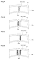
- 2A to 2D are enlarged views showing specific examples of markings formed on the second flange surface on the second optical surface side.
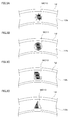
- 3A to 3D are enlarged views showing another specific example of the marking formed on the second flange surface on the second optical surface side.
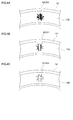
- 4A to 4C are enlarged views showing other specific examples of the marking formed on the second flange surface on the second optical surface side.
- FIG. 8A is a side sectional view of a collimating lens that is an optical element of the third embodiment
- FIG. 8B is a plan view of the collimating lens shown in FIG. 8A.
- a first-type objective lens 10 shown in FIGS. 1A and 1B is made of plastic and has a circular optical function part 11 having an optical function, and an annular flange convex provided radially outward from the outer edge of the optical function part 11. Part 12 and an annular flange neck part 13 interposed between optical function part 11 and flange convex part 12.
- the objective lens 10 is an objective lens for an optical pickup device having an NA of 0.75 or more.
- optical information corresponding to a BD (Blu-Ray Disc) standard with a wavelength of 405 nm and NA of 0.85 can be read or written.
- the optical function unit 11 of the objective lens 10 has a convex first optical surface OS1 having a relatively large curvature on the front side, and a convex second optical surface OS2 having a smaller curvature than the first optical surface OS1 on the back side.
- the first optical surface OS1 is disposed closer to a laser light source for writing (recording) or reading (reproducing) when the objective lens 10 is incorporated in an optical pickup device and operated.
- the second optical surface OS2 is disposed to face the optical information recording medium (specifically, BD) when the objective lens 10 is incorporated in the optical pickup device and operated.
- the first optical surface OS1 is a smooth mirror surface, a fine structure or a fine shape which is a diffractive structure can be provided.
- the second optical surface OS2 is a smooth mirror surface having no diffractive structure.
- An annular end surface EP0 is formed outside the second optical surface OS2.
- the inner end surface EP0 has, for example, a flat mirror surface that regularly reflects collimated light, and is used when the objective lens 10 is aligned.
- the objective lens 10 is not only the BD, but also a DVD (Digital Versatile Disc) with a wavelength of 655 nm and NA of 0.55 with a wavelength of 780 nm. It can function as a single-wave objective lens of a multiple wavelength compatible type that enables reading or writing of optical information corresponding to the CD (CompactCompDisc) standard.
- CD CompactCompDisc
- the flange convex portion 12 is an annular protrusion provided on the outer side in the radial direction of the flange neck portion 13, and is relatively thicker than the flange neck portion 13. That is, the flange convex portion 12 protrudes from the flange neck portion 13 on the laser light source side, that is, the first optical surface OS1 side, and also on the optical information recording medium side, that is, the second optical surface OS2 side.
- the flange convex portion 12 has a first flange surface 12a on the first optical surface OS1 side, a second flange surface 12b on the second optical surface OS2 side, and is outside the first and second flange surfaces 12a and 12b. Adjacent to the outer surface 12c.
- the first and second flange surfaces 12a and 12b are flat surfaces extending perpendicularly to the lens optical axis OA, and the outer diameter surface 12c is a cylindrical surface extending parallel to the lens optical axis OA.
- the coma aberration mark MC indicating the coma aberration state is formed on the second flange surface 12b on the optical information recording medium side, as will be described in detail later.
- a flat notched gate cut portion 14 is formed on a part of the outer periphery of the flange convex portion 12.
- the gate cut portion 14 is a mark obtained by removing the gate portion formed when the objective lens 10 is molded, and has a flat cut surface 14a extending parallel to the lens optical axis OA.
- the gate cut portion 14 indicates the gate position at the time of molding, and indicates the basic orientation of the objective lens 10.
- the flange neck part 13 is a thinner part than the optical function part 11 and the flange convex part 12.
- FIG. A ring-shaped first end surface EP1 is formed on the laser light source side of the flange neck portion 13, that is, the first optical surface OS1, and a ring-shaped first end surface EP1 is formed on the optical information recording medium side, that is, the second optical surface OS2.
- Two end surfaces EP2 are formed.
- the first and second end surfaces EP1, EP2 are mirror surfaces.
- the second type objective lens 10 shown in FIGS. 1A and 1C is made of glass, and most of them are the same as the plastic objective lens shown in FIG. 1B. Since it is not necessary, there is no gate cut portion, and the outer peripheral portion of the flange portion has a full circle. In the description of the second type objective lens 10, FIG. 1A is used in common with the first type objective lens 10.
- the size of the objective lens 10 shown in FIGS. 1A, 1B, and 1C will be described below.
- the total diameter of the objective lens including the flange convex portion 12 and the optical function portion 11 of the objective lens 10 is 3.5 mm.
- the surface diameter of the first optical surface OS1 is 2.57 mm, and the effective diameter of the first optical surface OS1 is 2.42 mm.
- the surface diameter of the second optical surface OS2 is 1.80 mm, and the effective diameter of the second optical surface OS2 is 1.59 mm.
- the lens thickness on the lens optical axis OA is 1.75 mm.
- the difference in height in the lens optical axis OA direction between the second flange surface 12b and the second end surface EP2 is 0.025 mm
- the height difference in the lens optical axis OA direction between the second end surface EP2 and the inner end surface EP0 is 0.023 mm
- the amount of flat placement that is, the difference in height in the lens optical axis OA direction between the second flange surface 12b and the most central portion of the second optical surface OS2 is 0.02 mm.
- the difference in height between the first flange surface 12a and the second flange surface 12b in the lens optical axis OA direction is 0.62 mm.
- the thickness ratio obtained by taking the ratio of the thickest portion (on the lens optical axis OA) in the lens optical axis OA direction and the thinnest portion in the lens optical axis OA direction is 3.63. .
- FIG. 2A is a diagram for explaining a specific coma aberration mark formed on the flange convex portion 12 which is a part of the flange portion 16 of the objective lens 10.
- a coma aberration mark MC0 is printed at one place on the circumference of the second flange surface 12b on the optical information recording medium side of the flange protrusion 12.
- This coma aberration mark MC0 indicates the coma aberration azimuth of the objective lens 10. That is, the direction from the lens optical axis OA toward the coma aberration mark MC0 indicates the directionality of the coma aberration.
- the coma aberration mark MC0 on the second flange surface 12b is not limited to that shown in FIG.
- the coma aberration marks MC0 to MC3 all indicate the coma aberration direction, but the coma aberration mark MC0 means that the amount of coma aberration is relatively small, and the coma aberration mark MC3 is coma aberration.
- the coma aberration marks MC1 and MC2 mean that the amount of coma is intermediate. That is, the coma aberration mark portion SHa constituting the coma aberration marks MC0 to MC3 represents the degree of coma aberration.
- the flange convex portion 12 is used when the objective lens 10 is fixed to the holder 40.
- the first flange surface 12a of the flange convex portion 12 abuts on the stepped portion in the holder 40, and the second flange surface 12b is exposed to the optical information recording medium side, so that the coma on the exposed second flange surface 12b.
- the aberration mark MC (MC0 to MC3) is formed, the objective lens 10 can be fixed to the holder 40 in an appropriate posture while observing the coma aberration mark MC.
- the size of the coma aberration mark MC is not more than the width of the second flange surface 12b. However, there is no particular limitation on the size in the circumferential direction along the ring-shaped second flange surface 12b. Considering the workability of observation when assembling the objective lens 10 to the holder 40, the size of the coma aberration mark MC needs to take into account the magnification and resolution upon observation with the naked eye or camera.
- the coma aberration mark MC can be written by reducing the coma aberration mark MC. Further, the coma aberration mark MC can be formed at two positions on both ends of the gate cut portion 14. Furthermore, a coma aberration mark MC may be formed on the opposite side of the gate cut portion 14 across the lens optical axis OA, and a mark indicating that the direction is reversed may be added.
- the color of the coma aberration mark MC black is used in the embodiment, but there is no particular limitation.
- the coma aberration mark MC needs to be formed of a material other than a non-colored and transparent material. It is formed of a chromatic light scatterer, an achromatic or chromatic absorber, or a light shield.
- the coma aberration mark MC was specifically formed using an inkjet.
- Inkjet can print a desired pattern at a desired position with a simple program, can suppress the influence of printing on the underlying material relatively little, and can minimize contamination of a non-printed portion. It has been confirmed that application using an inkjet is effective for forming the minute coma aberration mark MC as in the present embodiment.
- a paint used for inkjet an ink obtained by adding a dye to a UV curable resin material, an ink obtained by adding a dye to methyl ethyl ketone, or the like can be used.
- Various patterns including characters and the like can be printed by printing by applying these inks by an ink jet method.
- UV curable ink since the curing time can be shortened, marking can be performed efficiently in a short time.
- UV curable ink and methyl ethyl ketone ink have good adhesion to plastic and glass, and have environmental resistance such that they are difficult to peel off by wiping.
- a mold identification mark 31 is also formed on the second flange surface 12b of the flange convex portion 12 in addition to the coma aberration mark MC.
- the mold identification mark 31 is used to identify a mold used when the objective lens 10 is injection-molded or the like, and is not related to coma aberration and does not particularly indicate directionality.
- the mold identification mark 31 is called, for example, a dimple or the like, and has an unevenness or other three-dimensional shape transferred by the mold during molding.
- the mold identification mark 31 is not limited to being formed by a mold, but may be a ruled marking engraved with a sharp tool.
- FIGS. 3A to 3D show modified examples of the coma aberration marks MC0 to MC3 shown in FIGS. 2A to 2D.
- FIG. 3A shows a coma aberration mark MC10 having an irregular outline
- FIGS. 3B, 3C, and 3D show a ⁇ (circular) coma aberration mark MC11 and a ⁇ (square) coma aberration mark.
- MC12 and ⁇ (triangular) coma aberration mark MC13 are illustrated respectively.
- the degree of coma aberration can be expressed by the number of printed coma aberration marks MC10 to MC13, for example.
- FIGS. 2A to 2D show modified examples of the coma aberration marks MC0 to MC3 shown in FIGS. 2A to 2D.
- FIG. 4A shows a coma aberration mark MC20 having an irregular outline and colored in the first color
- FIG. 4B shows a coma aberration mark MC21 having an irregular outline and colored in the second color
- FIG. 4C shows a coma aberration mark MC22 having an irregular contour and colored in a third color.
- the positions of the coma aberration marks MC20 to MC22 indicate the direction of the coma aberration
- the colors of the coma aberration marks MC20 to MC22 indicate the degree of the coma aberration.
- the first to third colors assigned to the coma aberration marks MC20 to MC22 are not limited to chromatic colors but may be achromatic colors.
- FIG. 5 is a diagram conceptually illustrating a measurement printing apparatus 50 for measuring the coma aberration of the objective lens 10 and performing marking corresponding to the coma aberration.
- the illustrated measurement printing apparatus 50 includes a coma aberration measurement unit 51, a mark printing unit 53, and a conveyance support unit 55.
- the coma aberration measurement unit 51 measures the aberration of the objective lens 10 placed in a state of being positioned on the stage 56 of the transport support unit 55.
- the measured aberration includes an asymmetric aberration such as a coma aberration.
- the aberration direction of the objective lens 10 is, for example, the gate cut portion 14 (see FIG. 1B). Determined as a reference.
- the mark printing unit 53 can print the coma aberration mark MC at an appropriate position on the second flange surface 12b of the flange convex portion 12 of the objective lens 10 with UV curable ink, methyl ethyl ketone ink, or the like.
- the objective lens 10 on the stage 56 can be moved to adjust the printing position of the coma aberration mark MC, but the inkjet head of the mark printing unit 53 can also be moved relatively.
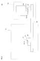
- FIG. 6 is a diagram for explaining the overall flow of the manufacturing process of the objective lens 10.
- the objective lens 10 is molded by injection molding (step S1). More specifically, a mold having a transfer surface corresponding to the first optical surface OS1 of the objective lens 10 and a mold having a transfer surface corresponding to the second optical surface OS2 are prepared, and both molds are positioned. Combine and close the mold. In this state, the resin is injected into a mold space formed between both molds and cured. Then, while removing both metal mold
- the objective lens 10 is not limited to being formed by injection molding of a thermoplastic resin or a thermosetting resin, but can also be formed of a UV curable resin.
- the objective lens 10 is formed by, for example, pressing of molten glass or softened glass.
- an antireflection coating is formed on the objective lens 10 (step S2). More specifically, the objective lens 10 is set in a vacuum vapor deposition apparatus, and the evaporated substance from the vapor deposition source is deposited on the first optical surface OS1 and the second optical surface OS2. At this time, the performance of the antireflection coating can be improved by using a plurality of vapor deposition sources.
- the antireflection coating can be formed by a method other than vacuum deposition. Further, the antireflection coating is not essential and can be replaced with a protective coating, for example.
- the objective lens 10 is set on the conveyance support unit 55 of the measurement printing apparatus 50 shown in FIG. 5, and the coma aberration measurement unit 51 measures the coma aberration of the objective lens 10 (step S3). More specifically, the wavefront is measured using, for example, an interferometer, and the coma aberration of the objective lens 10 is determined. By measuring the coma aberration, the direction and amount of the coma aberration of the target objective lens 10 is measured and temporarily stored as vector coma aberration data. This coma aberration data is transmitted to the mark printing unit 53.
- the coma aberration measuring unit 51 is an interferometer or the like, not only coma aberration but also spherical aberration, astigmatism and the like can be measured.
- the objective lens 10 is conveyed to the mark printing unit 53 by the conveyance support unit 55, and the coma aberration mark MC corresponding to the coma aberration measured on the objective lens 10 is printed on the flange convex portion 12 (step S4).
- the mark printing unit 53 selects appropriate pattern data from, for example, coma aberration marks MC0 to MC3 as shown in FIGS. 2A to 2D on the basis of the coma aberration data obtained in step S3, and the flange convex portion. Printing corresponding to the selected pattern data is performed at a position corresponding to the coma aberration direction of the 12 annular second flange surfaces 12b.
- the objective lens 10 in which the coma aberration mark MC (specifically, MC0 to MC3, etc.) as shown in FIG. 1B is formed.
- the coma aberration mark MC is made of an ink obtained by adding a dye to a UV curable resin material
- the second flange surface 12b is obtained by irradiating the ink applied on the second flange surface 12b with ultraviolet light.
- the upper ink is cured with a sufficient adhesion force to form the coma aberration mark MC.
- the coma aberration mark MC corresponding to the direction and degree of coma aberration is formed on the second flange surface (surface) 12b of the flange convex portion 12 of the objective lens (optical element) 10.
- the direction and degree of coma aberration can be directly grasped by the coma aberration mark MC.
- optical element and the method for manufacturing the optical element according to the second embodiment of the present invention will be described below. Note that the optical elements and the like of the second embodiment are obtained by partially changing the optical elements and the like of the first embodiment, and parts not specifically described are the same as those of the first embodiment.
- FIG. 7 is a plan view of the objective lens of the present embodiment on the information recording medium side.
- the coma aberration mark MC and the astigmatism mark MA are printed on the annular second flange surface 12b of the flange convex portion 12 provided on the flange portion 16. That is, the objective lens 10 has information on the direction and degree of coma and information on the direction and degree of astigmatism.
- FIG. 8A is a side sectional view of a collimating lens which is an optical element of the first embodiment
- FIG. 8B is a plan view of the collimating lens.
- the collimating lens 110 is made of plastic, and includes a circular optical function part 111 having an optical function, and an annular flange part 116 provided radially outward from the outer edge of the optical function part 111.
- the optical function unit 111 has a concave first optical surface OS3 on the side close to the laser light source, and a convex second optical surface OS4 on the side close to the objective lens 10 or the optical information recording medium.
- the flange portion 116 has a first flange surface 12a on the first optical surface OS3 side, a second flange surface 12b on the second optical surface OS4 side, and outside the first and second flange surfaces 12a and 12b. Adjacent to the outer diameter surface 12c.
- the coma aberration mark MC indicating the state of coma aberration is formed on the second flange surface 12b.
- a type identification mark 31 is also formed on the second flange surface 12b.
- the second flange surface 12b is exposed when the collimating lens 110 is attached to the holder, so that the coma aberration mark MC is formed on the second flange surface 12b.
- the coma aberration mark MC corresponding to the direction and degree of coma aberration is formed on the second flange surface (surface) 12b of the flange portion 116 of the collimating lens (optical element) 110.
- the direction and degree of coma aberration can be directly grasped by MC. Thereby, it is possible to provide a highly accurate optical pickup device while improving the workability of assembling the collimator lens 110.
- the coma aberration mark MC or the like can be printed on the flange convex portion of a beam shaper or the like incorporated in the optical pickup device.
- the size of the coma aberration mark MC is shown by changing the pattern of the coma aberration mark MC (including the number of components in the large pattern) and the color, but the size of the coma aberration mark MC is changed. It can also be used as an index of the magnitude of coma.
- the coma aberration mark MC or the like is provided on the second flange surface 12b of the flange convex portion 12, but the coma aberration mark MC or the like may be provided on the second end surface EP2 of the flange neck portion 13.
- the coma aberration mark MC and the astigmatism mark MA are formed on the second flange surface 12b of the flange convex portion 12.
- the coma aberration mark MC and astigmatism are formed on the first flange surface 12a on the opposite side.
- An aberration mark MA can also be formed.
- optical surfaces OS1 and OS2 provided on the objective lens 10 and the optical surfaces OS3 and OS4 provided on the collimating lens 110 are merely examples, and can be changed to various curved surfaces, stepped surfaces, and the like according to applications.
Landscapes
- Physics & Mathematics (AREA)
- Optics & Photonics (AREA)
- Engineering & Computer Science (AREA)
- General Physics & Mathematics (AREA)
- Manufacturing & Machinery (AREA)
- Mechanical Engineering (AREA)
- Health & Medical Sciences (AREA)
- Ophthalmology & Optometry (AREA)
- Optical Head (AREA)
Abstract
コマ収差の方向を簡易に把握できる光ピックアップ装置用の光学素子の製造方法を提供する。 対物レンズ10のフランジ凸部12の第2フランジ面12bにコマ収差の方向及び程度に対応するコマ収差マークMCを形成するので、コマ収差マークMCによってコマ収差の方向や程度を直接的に把握できる。これにより、対物レンズ10の組み付けの作業性を高めつつ、高精度の光ピックアップ装置を提供することができる。
Description
本発明は、光ピックアップ装置用の光学素子の製造方法及びこれによって得られる光ピックアップ装置用の光学素子に関する。
光ピックアップ装置等に用いられるプラスチックレンズとして、成形に付随して形成されるゲート位置を識別可能にするため、フランジ凸部においてゲート位置付近にゲート位置マークを付加したものが存在する(特許文献1参照)。この文献では、ゲート位置マークをインクジェットで形成すること、マークの色や形状を変更することについても、記載されている。
ところで、プラスチックレンズの性能は、一般にゲート位置との関連性が高いといえるが、ゲート位置を特定方向に設定して光ピックアップ装置に組み込んでも必ずしも所期の性能が得られるとはいえない。つまり、プラスチックレンズを光ピックアップ装置に組み込む場合、ゲート位置よりも実際のコマ収差等の方向を把握することの方が本来重要である。特に、BD(Blu-ray Disc)用の対物レンズでは、コマ収差の方向等を把握して光ピックアップ装置に組み込むことが重要になってきている。また、BD用の対物レンズについては、ガラスレンズが用いられる場合もあり、この場合、通常ゲート位置が存在しない。
本発明は、上述のような背景に鑑みてなされたものであり、コマ収差の方向を簡易に把握できる光ピックアップ装置用の光学素子の製造方法を提供することを目的とする。
また、本発明は、コマ収差の方向を簡易に把握できる光ピックアップ装置用の光学素子を提供することを目的とする。
上記課題を解決するため、本発明に係る光学素子の製造方法は、光ピックアップ装置用の光学素子を成形する工程と、成形した光学素子のコマ収差その他の収差を測定する工程と、測定値に基づき光学素子のフランジ部の表面にコマ収差の方向を示すマークを形成する工程とを備える。
上記の製造方法では、光学素子のフランジ部の表面にコマ収差の方向に対応するマークを形成するので、マークによってコマ収差の方向等を直接的に把握できる。これにより、光学素子の組み付けの作業性を高めつつ、高精度の光ピックアップ装置を提供することができる。
本発明に係る光学素子の製造方法の具体的な側面では、光学素子の成形と測定との間に、光学素子の光学面上に反射防止コートを成膜する工程を備える。この場合、反射防止コートを含めた使用状態に近い状態に相当するコマ収差をマークから把握できる。
本発明の別の側面では、マークが、インクジェットによって形成される。この場合、マークの形成すなわちマーキングをより簡易で迅速なものとすることができる。
本発明のさらに別の側面では、マークが、UV硬化型の樹脂を含有する塗料を用いて形成される。UV硬化型の樹脂を含有する塗料を用いることで、短時間で効率の良いマーキングが可能になる。
本発明のさらに別の側面では、マークが、メチルケトンを含有する塗料を用いて形成される。メチルケトンを含有する塗料を用いることで、特にガラスレンズでマークの輪郭形状の制御が容易になる。
本発明のさらに別の側面では、測定されたコマ収差その他の収差の大きさに応じて、マークの数、色、及びサイズのいずれかを変える。この場合、コマ収差の方向だけでなく大きさも把握することができ、光学素子の組み付けの作業性をより高めることができ、光ピックアップ装置の高精度化がより容易になる。
本発明のさらに別の側面では、光学素子のコマ収差及び非点収差を測定する工程を備え、コマ収差及び非点収差の測定後の光学素子のフランジ部に、コマ収差及び非点収差の方向を示すマークを形成する。この場合、コマ収差だけでなく非点収差も把握することができ、光学素子の組み付けの作業性をより高めることができ、光ピックアップ装置の高精度化がより容易になる。
本発明のさらに別の側面では、光学素子が、光ピックアップ装置用の対物レンズである。対物レンズは、コマ収差等の発生も大きくなりがちなので、コマ収差の方向等の管理が重要になってくる。
本発明のさらに別の側面では、光学素子は、コリメートレンズである。
また、本発明に係る光ピックアップ装置用の光学素子は、第1及び第2の光学面を有する本体部と、本体部の周囲に設けられたフランジ部とを有し、フランジ部の表面にコマ収差の方向に対応するマークを有する。
上記の光学素子では、フランジ部の表面にコマ収差の方向に対応するマークを有するので、マークによってコマ収差の方向等を直接的に把握できる。これにより、光学素子の組み付けの作業性を高めつつ、高精度の光ピックアップ装置を提供することができる。
本発明に係る光ピックアップ装置用の光学素子の具体的な側面では、情報記録媒体に対向して配置される対物レンズとして用いられ、マークが、フランジ部の情報記録媒体側に対応する第2光学面の周囲の平面上に形成されている。対物レンズの場合、マークが情報記録媒体側の平面上に形成されることで、レンズホルダーへの組み付けが容易になる。なお、上記第2光学面の周囲の平面には、第2フランジ面が含まれる。
本発明の別の側面では、マークが、UV硬化型の樹脂及びメチルケトンのいずれかを含有する塗料で形成されている。
本発明のさらに別の側面では、フランジ部に非点収差の方向に対応するマークをさらに有する。
〔第1実施形態〕
以下、図面を参照しつつ、本発明に係る第1実施形態の光学素子及び光学素子の製造方法について説明する。
以下、図面を参照しつつ、本発明に係る第1実施形態の光学素子及び光学素子の製造方法について説明する。
図1A及び1Bに示す第1タイプの対物レンズ10は、プラスチック製で、光学的機能を有する円形の光学機能部11と、光学機能部11の外縁から半径方向外側に設けられた環状のフランジ凸部12と、光学機能部11とフランジ凸部12との間に介在する環状のフランジネック部13とを備える。ここで、フランジ凸部12とフランジネック部13とを合わせたものがフランジ部16を構成する。この対物レンズ10は、NA0.75以上の光ピックアップ装置用の対物レンズである。具体的には、例えば波長405nmでNA0.85のBD(Blu-Ray Disc)の規格に対応した光情報の読み取り又は書き込みを可能とする。
対物レンズ10のうち光学機能部11は、表側に曲率の比較的大きな凸の第1光学面OS1を有し、裏側に第1光学面OS1よりも曲率の小さな凸の第2光学面OS2を有する。このうち、第1光学面OS1は、対物レンズ10を光ピックアップ装置に組み込んで動作させる際に、書き込み(記録)又は読み取り(再生)用のレーザー光源により近い側に配置される。また、第2光学面OS2は、対物レンズ10を光ピックアップ装置に組み込んで動作させる際に、光情報記録媒体(具体的には、BD)に対向して配置される。第1光学面OS1は、滑らかな鏡面となっているが、回折構造である微細構造又は微細形状を設けることもできる。一方、第2光学面OS2は、回折構造等を有しない滑らかな鏡面となっている。第2光学面OS2の外側には、輪帯状の内側端面EP0が形成されている。内側端面EP0は、例えばコリメート光を正反射する平坦な鏡面からなる領域を有しており、対物レンズ10をアライメントする際に利用される。
なお、第1光学面OS1に微細構造又は微細形状を設ける場合、対物レンズ10を、上記BDだけでなく、波長655nmでNA0.65のDVD(Digital Versatile Disc)や、波長780nmでNA0.53のCD(Compact Disc)の規格に対応した光情報の読み取り又は書き込みを可能とする複数波長互換タイプの単玉対物レンズとして機能させることができる。
フランジ凸部12は、フランジネック部13の半径方向外側に設けられた環状の突起部分であり、フランジネック部13よりも比較的肉厚となっている。つまり、フランジ凸部12は、フランジネック部13よりもレーザー光源側すなわち第1光学面OS1側において突起し、光情報記録媒体側すなわち第2光学面OS2側においても突起している。フランジ凸部12は、第1光学面OS1側において第1フランジ面12aを有し、第2光学面OS2側において第2フランジ面12bを有し、第1及び第2フランジ面12a,12bの外側に隣接して外径面12cを有する。第1及び第2フランジ面12a,12bは、レンズ光軸OAに垂直に延びる平坦な面となっており、外径面12cは、レンズ光軸OAに平行に延びる円筒面となっている。以上のうち光情報記録媒体側の第2フランジ面12bには、詳細は後述するが、コマ収差の状態を示すコマ収差マークMCが形成されている。なお、図1Bに示すように、フランジ凸部12の外周の一部には、平坦な切欠き状のゲートカット部14が形成されている。このゲートカット部14は、対物レンズ10の成形時に形成されるゲート部を除去した跡であり、レンズ光軸OAに平行に延びる平坦なカット面14aを有している。ゲートカット部14は、成形時のゲート位置を示すものであり、対物レンズ10の基本的な方位を示すものとなっている。
フランジネック部13は、光学機能部11及びフランジ凸部12よりも肉薄の部分である。フランジネック部13のレーザー光源側すなわち第1光学面OS1側には、輪帯状の第1端面EP1が形成されており、光情報記録媒体側すなわち第2光学面OS2側には、輪帯状の第2端面EP2が形成されている。第1及び第2端面EP1,EP2は、鏡面となっている。
また、図1A及び1Cに示す第2タイプの対物レンズ10は、ガラス製で、殆どが前述の図1Bに示したプラスチック製の対物レンズと共通しているが、ガラスレンズの製造にはゲートが必要ないため、ゲートカット部が存在せず、フランジ部の外周部が全周円状となっている。なお、第2タイプの対物レンズ10の説明において、図1Aを第1タイプの対物レンズ10と共通して用いている。
図1A、1B、及び1Cに示す対物レンズ10の大きさについて以下に記載する。対物レンズ10のフランジ凸部12及び光学機能部11等全てを含む対物レンズ全径は3.5mmである。また、第1光学面OS1の面径は2.57mmであり、第1光学面OS1の有効径は2.42mmである。さらに、第2光学面OS2の面径は1.80mmであり、第2光学面OS2の有効径は1.59mmである。また、レンズ光軸OA上のレンズ厚さは1.75mmである。また、第2フランジ面12bと第2端面EP2とのレンズ光軸OA方向の高さの差は0.025mmであり、第2端面EP2と内側端面EP0とのレンズ光軸OA方向の高さの差は0.023mmである。なお、平置き量、即ち、第2フランジ面12bと第2光学面OS2の最も中心部とのレンズ光軸OA方向の高さの差は、0.02mmである。また、第1フランジ面12aと第2フランジ面12bとのレンズ光軸OA方向の高さの差は0.62mmである。本対物レンズ10において、レンズ光軸OA方向に最も厚い部分(レンズ光軸OA上)とレンズ光軸OA方向に最も薄い部分との比を取った偏肉比の値は、3.63である。
図2Aは、対物レンズ10のフランジ部16の一部であるフランジ凸部12に形成される具体的なコマ収差マークについて説明する図である。フランジ凸部12の光情報記録媒体側の第2フランジ面12bには、円周の一箇所において、コマ収差マークMC0が印刷されている。このコマ収差マークMC0は、対物レンズ10のコマ収差の方位を示している。つまり、レンズ光軸OAからコマ収差マークMC0に向けての方向がコマ収差の方向性を示している。第2フランジ面12b上のコマ収差マークMC0は、図2Aに示すものに限らず、図2B~2Dに示すコマ収差マークMC1~MC3に変更できる。ここで、コマ収差マークMC0~MC3は、いずれもコマ収差の方位を示しているが、コマ収差マークMC0は、コマ収差の量が比較的小さいことを意味し、コマ収差マークMC3は、コマ収差の量が比較的大きいことを意味し、コマ収差マークMC1,MC2は、コマ収差の量が中間的であることを意味する。つまり、コマ収差マークMC0~MC3を構成するコマ収差マーク部分SHaは、コマ収差の程度を表している。以上のようなコマ収差マークMC0~MC3を利用することで、対物レンズ10のコマ収差を一種の簡易なベクトルとして表示することができる。
ここで、フランジ凸部12のうち特に第2フランジ面12bにコマ収差の指標としてのコマ収差マークMCを形成する理由について説明する。図1Aに示すように、フランジ凸部12は、対物レンズ10をホルダー40に固定する際に利用される。この際、フランジ凸部12の第1フランジ面12aがホルダー40内の段部に当接し、第2フランジ面12bが光情報記録媒体側に露出するので、露出する第2フランジ面12b上にコマ収差マークMC(MC0~MC3)を形成すれば、コマ収差マークMCを観察しながら対物レンズ10をホルダー40に対して適切な姿勢で固定することができる。
コマ収差マークMCのサイズは、第2フランジ面12bの幅以下とする。ただし、輪帯状の第2フランジ面12bに沿った周方向のサイズについては、特に制限がない。対物レンズ10をホルダー40に組み付ける際の観察の作業性を考えた場合、コマ収差マークMCのサイズは、肉眼又はカメラによる観察に際しての倍率や分解能が考慮されたものとする必要がある。
なお、コマ収差の方向がゲートカット部14と一致する場合、コマ収差マークMCを小さくすることで、コマ収差マークMCの書き込みが可能になる。また、ゲートカット部14の両端の2箇所にコマ収差マークMCを形成することもできる。さらに、レンズ光軸OAを挟んでゲートカット部14の反対側にコマ収差マークMCを形成し、方向が反転していることを意味するマークを追加することもできる。
コマ収差マークMCの色については、実施例では黒色系を用いているが、特に制限がない。対物レンズ10をホルダー40に組み付ける際のコマ収差マークMCの検出性を考えた場合、コマ収差マークMCは、無着色で透明色の材料以外のもので形成する必要があり、例えば無彩色又は有彩色の光散乱体、無彩色又は有彩色の吸収体又は遮光体等で形成することになる。
コマ収差マークMCは、簡便性を考慮して、具体的にはインクジェットを利用して形成された。インクジェットは、簡易なプログラムで所望のパターンを所望の位置に印刷することができ、印刷の下地材料に対する影響を比較的少なく抑えることができ、印刷しない部分の汚染も最小限とできる。本実施形態のような微小なコマ収差マークMCの形成には、インクジェットを利用した塗布が有効であることを確認している。インクジェットに用いる塗料としては、UV硬化性の樹脂材料に色素を添加したインク、メチルエチルケトンに色素を添加したインク等を用いることができる。これらのインクをインクジェット方式で塗布する印刷により、文字等を含む様々なパターンの印刷が可能である。特にUV硬化性のインクの場合、硬化時間を短くできるので、短時間で効率良くマーキングを行うことができる。また、UV硬化性のインクやメチルエチルケトンのインクは、プラスチックやガラスに対する付着性が良好であり、拭き取りによって剥がれにくいという環境的な耐性を有する。
図1B及び1Cに示すように、フランジ凸部12の第2フランジ面12bには、コマ収差マークMCのほかに、型識別マーク31も形成されている。この型識別マーク31は、対物レンズ10を射出成形等する際に利用した成形型を識別するためのものであり、コマ収差とは関係がなく特に方向性を示すものでもない。型識別マーク31は、例えばディンプル等と呼ばれ、成形時に成形型によって転写される凹凸その他の立体形状である。型識別マーク31は、成形型によって形成されるものに限らず、鋭利な工具によって刻設した罫書きからなるものとできる。
図3A~3Dは、図2A~2Dに示すコマ収差マークMC0~MC3の変形例を示している。図3Aは、不規則な輪郭を有するコマ収差マークMC10を示しており、図3B、3C、及び3Dは、○型(円型)のコマ収差マークMC11、□型(四角型)のコマ収差マークMC12、及び△型(三角型)のコマ収差マークMC13をそれぞれ例示している。なお、コマ収差の程度は、例えばコマ収差マークMC10~MC13の印刷個数によって表現することができる。
図4A~4Cは、図2A~2Dに示すコマ収差マークMC0~MC3の変形例を示している。図4Aは、不規則な輪郭を有し第1色に着色されたコマ収差マークMC20を示しており、図4Bは、不規則な輪郭を有し第2色に着色されたコマ収差マークMC21を示しており、図4Cは、不規則な輪郭を有し第3色に着色されたコマ収差マークMC22を示している。これらのコマ収差マークMC20~MC22の位置は、コマ収差の方向を示し、コマ収差マークMC20~MC22の色は、コマ収差の程度を示すものとする。ここで、コマ収差マークMC20~MC22に割り当てられる第1~3色は、有彩色に限らず無彩色とすることができる。
図5は、対物レンズ10のコマ収差を測定しコマ収差に対応するマーキングを行うための測定印刷装置50を概念的に説明する図である。図示の測定印刷装置50は、コマ収差測定部51と、マーク印刷部53と、搬送支持部55とを備える。コマ収差測定部51は、搬送支持部55のステージ56上に位置決めした状態で載置された対物レンズ10の収差を計測する。計測される収差には、コマ収差等の非対称的な収差が含まれており、コマ収差等の非対称的な収差については、対物レンズ10の収差方向が例えばゲートカット部14(図1B参照)を基準として決定される。マーク印刷部53は、対物レンズ10のうちフランジ凸部12の第2フランジ面12bの適所に、UV硬化性のインク、メチルエチルケトンのインク等によって、コマ収差マークMCを印刷することができる。なお、コマ収差マークMCの印刷位置を調整するため、ステージ56上の対物レンズ10を移動させることもできるが、マーク印刷部53のインクジェットのヘッドを相対的に移動させることもできる。
図6は、対物レンズ10の製造工程の全体的な流れを説明する図である。まず、射出成形によって対物レンズ10を成形する(ステップS1)。より具体的には、対物レンズ10の第1光学面OS1に対応する転写面を有する成形型と、第2光学面OS2に対応する転写面を有する成形型とを準備し、両金型を位置合わせして型閉じ及び型締めを行う。この状態で、両金型間に形成された型空間中に樹脂を射出し硬化させる。その後、両金型を離間し硬化した成形品を取り出すとともに、成形品からゲート部等を除去することで、対物レンズ10が得られる。なお、対物レンズ10は、熱可塑性樹脂や熱硬化性樹脂の射出成形によって形成される場合に限らず、UV硬化性樹脂で形成することもできる。なお、対物レンズ10がガラス製である場合、対物レンズ10は、例えば溶融ガラスや軟化ガラスのプレスによって形成される。
次に、対物レンズ10に対して反射防止コートの成膜を行う(ステップS2)。より具体的には、対物レンズ10を真空蒸着装置内にセットし、蒸着源からの蒸発物質を第1光学面OS1と第2光学面OS2とに堆積させる。この際、複数の蒸着源を用いることで、反射防止コートの性能を高めることができる。なお、反射防止コートは、真空蒸着以外の手法で成膜することができる。また、反射防止コートについては、必須のものではなく、例えば保護コート等に置き換えることができる。
次に、図5に示す測定印刷装置50の搬送支持部55に対物レンズ10をセットし、コマ収差測定部51において対物レンズ10のコマ収差を測定する(ステップS3)。より具体的には、例えば干渉計を利用して波面を測定し、対物レンズ10のコマ収差を決定する。コマ収差の測定により、対象たる対物レンズ10のコマ収差の方向や量が測定され、ベクトル的なコマ収差データとして一旦保管される。このコマ収差データはマーク印刷部53に送信される。なお、コマ収差測定部51が干渉計等である場合、コマ収差に限らず、球面収差、非点収差等を測定することもできる。
次に、搬送支持部55によって対物レンズ10をマーク印刷部53に搬送し、対物レンズ10に測定したコマ収差に対応するコマ収差マークMCをフランジ凸部12に印刷する(ステップS4)。具体的には、マーク印刷部53において、ステップS3で得たコマ収差データに基づいて、例えば図2A~2Dに示すようなコマ収差マークMC0~MC3から適切なパターンデータを選択し、フランジ凸部12の環状の第2フランジ面12bのうちコマ収差の方向に対応する箇所において選択したパターンデータに対応する印刷を行う。これにより、図1Bに示すようなコマ収差マークMC(具体的にはMC0~MC3等)を形成した対物レンズ10を得ることができる。なお、コマ収差マークMCがUV硬化性の樹脂材料に色素を添加したインクからなる場合、第2フランジ面12b上に塗布されたインクに対して紫外光を照射することで、第2フランジ面12b上のインクを十分な付着力で硬化させて、コマ収差マークMCを形成することになる。
以上説明した第1実施形態によれば、対物レンズ(光学素子)10のフランジ凸部12の第2フランジ面(表面)12bにコマ収差の方向及び程度に対応するコマ収差マークMCを形成するので、コマ収差マークMCによってコマ収差の方向や程度を直接的に把握できる。これにより、対物レンズ10の組み付けの作業性を高めつつ、高精度の光ピックアップ装置を提供することができる。
〔第2実施形態〕
以下、本発明に係る第2実施形態の光学素子及び光学素子の製造方法について説明する。なお、第2実施形態の光学素子等は、第1実施形態の光学素子等を一部変更したものであり、特に説明しない部分は、第1実施形態と同様であるものとする。
以下、本発明に係る第2実施形態の光学素子及び光学素子の製造方法について説明する。なお、第2実施形態の光学素子等は、第1実施形態の光学素子等を一部変更したものであり、特に説明しない部分は、第1実施形態と同様であるものとする。
図7は、本実施形態の対物レンズの情報記録媒体側の平面図である。この場合、フランジ部16に設けたフランジ凸部12の環状の第2フランジ面12bにおいて、コマ収差マークMCと、非点収差マークMAとが印刷されている。つまり、この対物レンズ10は、コマ収差の方向及び程度に関する情報と、非点収差の方向及び程度に関する情報とを有している。
〔第3実施形態〕
以下、本発明に係る第3実施形態の光学素子及び光学素子の製造方法について説明する。なお、第3実施形態の光学素子等は、第1実施形態の光学素子等を一部変更したものであり、特に説明しない部分は、第1実施形態と同様であるものとする。
以下、本発明に係る第3実施形態の光学素子及び光学素子の製造方法について説明する。なお、第3実施形態の光学素子等は、第1実施形態の光学素子等を一部変更したものであり、特に説明しない部分は、第1実施形態と同様であるものとする。
図8Aは、第1実施形態の光学素子であるコリメートレンズの側方断面図であり、図8Bは、コリメートレンズの平面図である。
コリメートレンズ110は、プラスチック製で、光学的機能を有する円形の光学機能部111と、光学機能部111の外縁から半径方向外側に設けられた環状のフランジ部116とを備える。ここで、光学機能部111は、レーザー光源に近い側に凹の第1光学面OS3を有し、対物レンズ10又は光情報記録媒体に近い側に凸の第2光学面OS4を有する。フランジ部116は、第1光学面OS3側において第1フランジ面12aを有し、第2光学面OS4側において第2フランジ面12bを有し、第1及び第2フランジ面12a,12bの外側に隣接して外径面12cを有する。以上のうち第2フランジ面12bには、コマ収差の状態を示すコマ収差マークMCが形成されている。第2フランジ面12bには、コマ収差マークMCのほかに、型識別マーク31も形成されている。なお、このコリメートレンズ110の場合、ホルダーへの取り付けに際して第2フランジ面12bが露出するので、第2フランジ面12bにコマ収差マークMCが形成されている。
第3実施形態においても、コリメートレンズ(光学素子)110のフランジ部116の第2フランジ面(表面)12bに、コマ収差の方向及び程度に対応するコマ収差マークMCを形成するので、コマ収差マークMCによってコマ収差の方向や程度を直接的に把握できる。これにより、コリメートレンズ110の組み付けの作業性を高めつつ、高精度の光ピックアップ装置を提供することができる。
なお、以上のコリメートレンズ110と同様に、光ピックアップ装置に組み込まれるビームシェーパー等のフランジ凸部にもコマ収差マークMC等を印字することができる。
以上実施形態に即して本発明を説明したが、本発明は、上記実施形態に限定されるものではなく、種々の変形が可能である。
例えば、上記実施形態では、コマ収差マークMCのパターン(大きいパターン中の構成要素の個数を含む)や色を変化させてコマ収差の大きさを示したが、コマ収差マークMCのサイズを変化させてコマ収差の大きさの指標とすることもできる。
上記実施形態では、コマ収差マークMC等をフランジ凸部12の第2フランジ面12bに設けたが、コマ収差マークMC等をフランジネック部13の第2端面EP2に設けることもできる。
上記実施形態では、図7の対物レンズ10や図8のコリメートレンズ110がプラスチックレンズであることを前提として説明を行ったが、上記対物レンズ10やコリメートレンズ110はガラス製である場合もある。このような場合も、対物レンズ10のフランジ凸部12やコリメートレンズ110のフランジ凸部112にコマ収差マークMCや非点収差マークMAを印刷することができる。
また、以上の説明では、フランジ凸部12の第2フランジ面12bにコマ収差マークMCや非点収差マークMAを形成したが、反対側の第1フランジ面12a等にコマ収差マークMCや非点収差マークMAを形成することもできる。
また、対物レンズ10に設けた光学面OS1,OS2、コリメートレンズ110に設けた光学面OS3,OS4は単なる例示であり、用途等に応じて様々な曲面、段差面等に変更することができる。
Claims (13)
- 光ピックアップ装置用の光学素子を成形する工程と、
成形した前記光学素子の収差を測定する工程と、
測定値に基づき前記光学素子のフランジ部の表面にコマ収差の方向を示すマークを形成する工程とを備える光学素子の製造方法。 - 前記光学素子の成形と測定との間に、前記光学素子の光学面上に反射防止コートを成膜する工程を備える、請求項1に記載の光学素子の製造方法。
- 前記マークは、インクジェットによって形成される、請求項1及び2のいずれか一項に記載の光学素子の製造方法。
- 前記マークは、UV硬化型の樹脂を含有する塗料を用いて形成される、請求項3に記載の光学素子の製造方法。
- 前記マークは、メチルケトンを含有する塗料を用いて形成される、請求項3に記載の光学素子の製造方法。
- 測定されたコマ収差の大きさに応じて、前記マークの数、色、及びサイズのいずれかを変える、請求項1に記載の光学素子の製造方法。
- 前記光学素子のコマ収差及び非点収差を測定する工程を備え、コマ収差及び非点収差の測定後の前記光学素子の前記フランジ部に、コマ収差及び非点収差の方向を示すマークを形成する、請求項1に記載の光学素子の製造方法。
- 前記光学素子は、光ピックアップ装置用の対物レンズである、請求項1に記載の光学素子の製造方法。
- 前記光学素子は、コリメートレンズである、請求項1に記載の光学素子の製造方法。
- 第1及び第2の光学面を有する本体部と、前記本体部の周囲に設けられたフランジ部とを有し、
前記フランジ部の表面にコマ収差の方向に対応するマークを有する光ピックアップ装置用の光学素子。 - 情報記録媒体に対向して配置される対物レンズとして用いられ、前記マークは、前記フランジ部の情報記録媒体側に対応する前記第2光学面の周囲の平面上に形成されている、請求項10に記載の光ピックアップ装置用の光学素子。
- 前記マークは、UV硬化型の樹脂及びメチルケトンのいずれかを含有する塗料で形成されている、請求項10及び11のいずれか一項に記載の光ピックアップ装置用の光学素子。
- 前記フランジ部に非点収差の方向に対応するマークをさらに有する、請求項10に記載の光ピックアップ装置用の光学素子。
Priority Applications (1)
| Application Number | Priority Date | Filing Date | Title |
|---|---|---|---|
| JP2012558035A JPWO2012111803A1 (ja) | 2011-02-18 | 2012-02-17 | 光学素子の製造方法及び光ピックアップ装置用の光学素子 |
Applications Claiming Priority (2)
| Application Number | Priority Date | Filing Date | Title |
|---|---|---|---|
| JP2011034018 | 2011-02-18 | ||
| JP2011-034018 | 2011-02-18 |
Publications (1)
| Publication Number | Publication Date |
|---|---|
| WO2012111803A1 true WO2012111803A1 (ja) | 2012-08-23 |
Family
ID=46672714
Family Applications (1)
| Application Number | Title | Priority Date | Filing Date |
|---|---|---|---|
| PCT/JP2012/053809 Ceased WO2012111803A1 (ja) | 2011-02-18 | 2012-02-17 | 光学素子の製造方法及び光ピックアップ装置用の光学素子 |
Country Status (2)
| Country | Link |
|---|---|
| JP (1) | JPWO2012111803A1 (ja) |
| WO (1) | WO2012111803A1 (ja) |
Citations (2)
| Publication number | Priority date | Publication date | Assignee | Title |
|---|---|---|---|---|
| JP2004281035A (ja) * | 2003-02-28 | 2004-10-07 | Matsushita Electric Ind Co Ltd | 光ヘッド及びそれを備えた光記録再生装置 |
| JP2008275738A (ja) * | 2007-04-26 | 2008-11-13 | Konica Minolta Opto Inc | 光学素子及びその製造方法 |
-
2012
- 2012-02-17 JP JP2012558035A patent/JPWO2012111803A1/ja active Pending
- 2012-02-17 WO PCT/JP2012/053809 patent/WO2012111803A1/ja not_active Ceased
Patent Citations (2)
| Publication number | Priority date | Publication date | Assignee | Title |
|---|---|---|---|---|
| JP2004281035A (ja) * | 2003-02-28 | 2004-10-07 | Matsushita Electric Ind Co Ltd | 光ヘッド及びそれを備えた光記録再生装置 |
| JP2008275738A (ja) * | 2007-04-26 | 2008-11-13 | Konica Minolta Opto Inc | 光学素子及びその製造方法 |
Also Published As
| Publication number | Publication date |
|---|---|
| JPWO2012111803A1 (ja) | 2014-07-07 |
Similar Documents
| Publication | Publication Date | Title |
|---|---|---|
| US6914724B2 (en) | Micro lens and method and apparatus for fabricating | |
| US11543680B2 (en) | Spectacle lens and method for producing same | |
| JP6105205B2 (ja) | 光学レンズ | |
| JP5076618B2 (ja) | 光ピックアップ装置用のガラス製レンズ | |
| WO2012111803A1 (ja) | 光学素子の製造方法及び光ピックアップ装置用の光学素子 | |
| JP2004295998A (ja) | 対物レンズ、光ピックアップ装置、及び光情報記録再生装置 | |
| JPS62238502A (ja) | グレ−テイングレンズ | |
| KR20030087002A (ko) | 광학픽업용 대물렌즈, 광학픽업 및 광디스크장치 | |
| WO2013094173A1 (ja) | 対物レンズ、光ピックアップ、光ディスク装置、樹脂成形用金型及び対物レンズの製造方法 | |
| Beich | Injection molded polymer optics in the 21st-Century | |
| JP2005038581A (ja) | 光学素子及び光ピックアップ装置 | |
| JP5119080B2 (ja) | 光学記録読み取り用ピックアップ用光学素子 | |
| JPH0482112B2 (ja) | ||
| US20130142968A1 (en) | Optical recording media with specific vision label layer | |
| WO2011013339A1 (ja) | 光ピックアップレンズ | |
| US20050117222A1 (en) | Precise optical grating element and method of making a stamper thereof | |
| JPS6167013A (ja) | オプテイカル デイスク プレーヤー用レンズ | |
| JP3088128B2 (ja) | 対物レンズの調整方法 | |
| Schaub | Plastic Optics | |
| WO2008055104A2 (en) | Device and method for maintaining optical energy density on a storage medium | |
| WO2004051636A2 (en) | Objective lens and scanning device using such an objective lens | |
| JP2007079318A (ja) | 光学素子、そのマーキング方法、及び光学ユニットの組立方法 | |
| US20070258099A1 (en) | Self-aligning color optical print head | |
| JP2008030160A (ja) | 円形レンズの心取り方法と該方法を用いた円形レンズの製造方法 | |
| Kojima | Advances in optical disk lens |
Legal Events
| Date | Code | Title | Description |
|---|---|---|---|
| 121 | Ep: the epo has been informed by wipo that ep was designated in this application |
Ref document number: 12747280 Country of ref document: EP Kind code of ref document: A1 |
|
| ENP | Entry into the national phase |
Ref document number: 2012558035 Country of ref document: JP Kind code of ref document: A |
|
| NENP | Non-entry into the national phase |
Ref country code: DE |
|
| 122 | Ep: pct application non-entry in european phase |
Ref document number: 12747280 Country of ref document: EP Kind code of ref document: A1 |